JP7301582B2 - Electrical contacts and electrical connecting devices - Google Patents
Electrical contacts and electrical connecting devices Download PDFInfo
- Publication number
- JP7301582B2 JP7301582B2 JP2019072224A JP2019072224A JP7301582B2 JP 7301582 B2 JP7301582 B2 JP 7301582B2 JP 2019072224 A JP2019072224 A JP 2019072224A JP 2019072224 A JP2019072224 A JP 2019072224A JP 7301582 B2 JP7301582 B2 JP 7301582B2
- Authority
- JP
- Japan
- Prior art keywords
- main body
- electrical
- extending
- base
- housing
- Prior art date
- Legal status (The legal status is an assumption and is not a legal conclusion. Google has not performed a legal analysis and makes no representation as to the accuracy of the status listed.)
- Active
Links
Images


Classifications
-
- G—PHYSICS
- G01—MEASURING; TESTING
- G01R—MEASURING ELECTRIC VARIABLES; MEASURING MAGNETIC VARIABLES
- G01R31/00—Arrangements for testing electric properties; Arrangements for locating electric faults; Arrangements for electrical testing characterised by what is being tested not provided for elsewhere
- G01R31/28—Testing of electronic circuits, e.g. by signal tracer
- G01R31/2851—Testing of integrated circuits [IC]
- G01R31/2886—Features relating to contacting the IC under test, e.g. probe heads; chucks
-
- G—PHYSICS
- G01—MEASURING; TESTING
- G01R—MEASURING ELECTRIC VARIABLES; MEASURING MAGNETIC VARIABLES
- G01R1/00—Details of instruments or arrangements of the types included in groups G01R5/00 - G01R13/00 and G01R31/00
- G01R1/02—General constructional details
- G01R1/04—Housings; Supporting members; Arrangements of terminals
- G01R1/0408—Test fixtures or contact fields; Connectors or connecting adaptors; Test clips; Test sockets
- G01R1/0433—Sockets for IC's or transistors
- G01R1/0441—Details
- G01R1/0466—Details concerning contact pieces or mechanical details, e.g. hinges or cams; Shielding
-
- G—PHYSICS
- G01—MEASURING; TESTING
- G01R—MEASURING ELECTRIC VARIABLES; MEASURING MAGNETIC VARIABLES
- G01R1/00—Details of instruments or arrangements of the types included in groups G01R5/00 - G01R13/00 and G01R31/00
- G01R1/02—General constructional details
- G01R1/04—Housings; Supporting members; Arrangements of terminals
- G01R1/0408—Test fixtures or contact fields; Connectors or connecting adaptors; Test clips; Test sockets
- G01R1/0416—Connectors, terminals
-
- H—ELECTRICITY
- H01—ELECTRIC ELEMENTS
- H01R—ELECTRICALLY-CONDUCTIVE CONNECTIONS; STRUCTURAL ASSOCIATIONS OF A PLURALITY OF MUTUALLY-INSULATED ELECTRICAL CONNECTING ELEMENTS; COUPLING DEVICES; CURRENT COLLECTORS
- H01R13/00—Details of coupling devices of the kinds covered by groups H01R12/70 or H01R24/00 - H01R33/00
- H01R13/02—Contact members
- H01R13/22—Contacts for co-operating by abutting
- H01R13/24—Contacts for co-operating by abutting resilient; resiliently-mounted
- H01R13/2407—Contacts for co-operating by abutting resilient; resiliently-mounted characterized by the resilient means
-
- H—ELECTRICITY
- H01—ELECTRIC ELEMENTS
- H01R—ELECTRICALLY-CONDUCTIVE CONNECTIONS; STRUCTURAL ASSOCIATIONS OF A PLURALITY OF MUTUALLY-INSULATED ELECTRICAL CONNECTING ELEMENTS; COUPLING DEVICES; CURRENT COLLECTORS
- H01R13/00—Details of coupling devices of the kinds covered by groups H01R12/70 or H01R24/00 - H01R33/00
- H01R13/02—Contact members
- H01R13/22—Contacts for co-operating by abutting
- H01R13/24—Contacts for co-operating by abutting resilient; resiliently-mounted
- H01R13/2442—Contacts for co-operating by abutting resilient; resiliently-mounted with a single cantilevered beam
-
- G—PHYSICS
- G01—MEASURING; TESTING
- G01R—MEASURING ELECTRIC VARIABLES; MEASURING MAGNETIC VARIABLES
- G01R1/00—Details of instruments or arrangements of the types included in groups G01R5/00 - G01R13/00 and G01R31/00
- G01R1/02—General constructional details
- G01R1/04—Housings; Supporting members; Arrangements of terminals
- G01R1/0408—Test fixtures or contact fields; Connectors or connecting adaptors; Test clips; Test sockets
- G01R1/0433—Sockets for IC's or transistors
- G01R1/0441—Details
- G01R1/0458—Details related to environmental aspects, e.g. temperature
Description
本発明は、電気的接続装置に関し、例えば、被検査体の通電試験に用いる電気的接触子及び電気的接続装置に適用し得るものである。 TECHNICAL FIELD The present invention relates to an electrical connection device, and is applicable, for example, to an electrical contactor and an electrical connection device used for an electrical test of a device under test.
従来、集積回路の製造過程では、パッケージされた集積回路について、例えばパッケージテスト、ファイナルテスト等と呼ばれる電気的特性の検査が行なわれる。そのような検査では、被検査体である集積回路を着脱可能に保持した状態で、その保持した集積回路の電極端子に電気的接触子を電気的接触させる電気的接続装置(いわゆるテストソケット等)が用いられる。電気的接続装置に装着された集積回路は、この電気的接続装置を介して検査装置(テスタ)に電気的に接続され、電気的特性の検査が行われる。 2. Description of the Related Art Conventionally, in the manufacturing process of an integrated circuit, the packaged integrated circuit is subjected to an electrical characteristic test called a package test, a final test, or the like. In such tests, an electrical connecting device (a so-called test socket, etc.) is used to electrically connect electrical contacts to the electrode terminals of the integrated circuit, which is an object to be inspected, while detachably holding the integrated circuit. is used. The integrated circuit mounted on the electrical connection device is electrically connected to an inspection device (tester) through the electrical connection device, and its electrical characteristics are inspected.
特許文献1には、ICデバイスの検査に使用される電気相互接続アッセンブリーが開示されている。電気相互接続アッセンブリーは複数の検査接点(電気的接触子)を有しており、各電気的接触子は、被検査体の電極端子を電気的に接続する第1電気接続部と、配線基板上の検査端子を電気的に接続するための第2電気接続部とを有する。複数の電気的接触子は、その配列方向に沿って、例えばエラストマ等で形成された、略円筒形状の付勢部材で支持されており、付勢部材は、第1電気接続部と第2電気接続部に弾性力を作用させることで、第1電気接続部と被検査体の電極端子との電気的接続性、第2電気接続部と配線基板の検査端子との電気的接続性を保持している。 US Pat. No. 6,200,000 discloses an electrical interconnect assembly for use in testing IC devices. The electrical interconnection assembly has a plurality of test contacts (electrical contacts), each electrical contact having a first electrical connection for electrically connecting an electrode terminal of the device under test and a and a second electrical connection for electrically connecting the inspection terminals of the. The plurality of electrical contacts are supported along their arrangement direction by a substantially cylindrical biasing member made of, for example, elastomer. By applying an elastic force to the connecting portion, the electrical connectivity between the first electrical connecting portion and the electrode terminal of the device under test and the electrical connectivity between the second electrical connecting portion and the inspection terminal of the wiring board are maintained. ing.
しかしながら、高温対応の集積回路の電気的特性を検査するためには、高温環境下で集積回路を検査することが要求されるが、特許文献1の記載技術のように、エラストマ等の付勢部材を有しているものは、高温環境下で当該部材が劣化し、電気的接触子と被検査体の電極端子との接触荷重が低下してしまうおそれがある。したがって、高温環境下で、電気的接触子と、被検査体の電極端子及び検査端子とが高荷重で電気的に接触させることが望まれる。 However, in order to test the electrical characteristics of a high-temperature integrated circuit, it is required to test the integrated circuit in a high-temperature environment. , the member may deteriorate in a high-temperature environment, and the contact load between the electrical contactor and the electrode terminal of the device to be tested may decrease. Therefore, it is desired to electrically contact the electrical contacts with the electrode terminals and inspection terminals of the device to be inspected under a high-temperature environment under a high load.
また、被検査体の電極端子と基板の端子とのそれぞれに電気的に接触させる複数の電気的接触子を電気的接続装置に装着する際、各電気的接触子の位置合わせの精度を向上させることが望まれる。 Further, when a plurality of electrical contactors for electrically contacting the electrode terminals of the device to be tested and the terminals of the substrate are attached to the electrical connecting device, the accuracy of alignment of each electrical contactor can be improved. is desired.
そのため、本発明は、高温環境下での電気的試験に対応可能であり、簡単かつ確実に位置決めすることができる電気的接触子及び電気的接続装置が求められている。 Therefore, the present invention requires an electrical contactor and an electrical connection device that can be applied to electrical tests in a high-temperature environment and that can be easily and reliably positioned.
かかる課題を解決するために、第1の本発明の電気的接触子は、上側部材と下側部材とで構成されたハウジングに収容されて使用される電気的接触子であって、(1)ハウジングの下側部材上に載置され、導電部材で形成された板状の本体部と、(2)本体部から一体的に連続して上方に延出した上部基部と、上部基部から本体部に沿って横方向に延出した上部支持部と、上部支持部から垂直上方に延出して第1の接触対象と電気的に接触する第1の先端部とを有する片持ち梁構造の上部アーム部と、(3)本体部から一体的に連続して下方に延出した下部基部と、下部基部から本体部に沿って横方向に延出した下部支持部と、下部支持部から垂直下方に延出して第2の接触対象と電気的に接触する第2の先端部とを有する片持ち梁構造の下部アーム部と、(4)本体部の一方の端部から上方に延出した第1の位置決め部と、(5)本体部の他方の端部付近から上方に延出した第2の位置決め部とを備え、上部アーム部は、ハウジングの上側部材に設けられた上下方向に貫通する開口部を通って配置し、下部アーム部は、ハウジングの下側部材に設けられた上下方向に貫通する開口部を通って配置し、第1の位置決め部が、ハウジングの上側部材の下面に設けられた第1の穴部に収納され、第2の位置決め部が、ハウジングの上側部材の下面に設けられた第2の穴部に収容されることを特徴とする。
In order to solve such a problem, a first electrical contact of the present invention is an electrical contact that is housed in a housing composed of an upper member and a lower member, comprising: (1) (2) a plate-like main body placed on the lower member of the housing and formed of a conductive member; (2) an upper base extending upward from the main body and continuing from the main body; and a first tip extending vertically upwardly from the upper support for making electrical contact with the first contact object. (3) a lower base extending integrally and continuously downward from the main body; a lower support extending laterally along the main body from the lower base; (4) a cantilever structure lower arm portion having a second distal end portion that extends to electrically contact a second contact target; and (5) a second positioning portion extending upward from the vicinity of the other end of the main body portion, and the upper arm portion extends through an opening vertically penetrating provided in the upper member of the housing. the lower arm portion is disposed through a vertically penetrating opening provided in the lower member of the housing; and the first positioning portion is provided on the lower surface of the upper member of the housing. and the second positioning portion is accommodated in a second hole provided in the lower surface of the upper member of the housing.
第2の本発明の電気的接触子は、第1の本発明の2個の電気的接触子と、複数の電気的接触子の間に挟まれた絶縁部材とを備えることを特徴とする。 An electrical contact according to the second aspect of the present invention comprises two electrical contacts according to the first aspect of the present invention and an insulating member sandwiched between the plurality of electrical contacts.
第3の本発明の電気的接続装置は、配線が形成された基板と、基板上に第1の本発明の複数の電気的接触子を収容するハウジング部と、ハウジング部に収容される前記複数の電気的接触子と接触可能な位置に被検査体を収容する被検査体収容部とを備え、各電気的接触子を介して、被検査体の電極部と前記基板の配線との間を電気的に接続させる電気的接続装置において、ハウジング部が、複数の電気的接触子を収容する収容内部の上面に、各電気的接触子の一方の端部にある第1の位置決め部を収容する第1の穴部と、各電気的接触子の他方の端部側にある第2の位置決め部を収容する第2の穴部とを備えることを特徴とする。 An electrical connecting device according to a third aspect of the present invention comprises a substrate on which wiring is formed, a housing portion for accommodating a plurality of electrical contacts according to the first aspect of the present invention on the substrate, and the plurality of electrical contacts accommodated in the housing portion. and an object-to-be-tested housing part for housing the object to be tested at a contactable position with the electrical contacts of the electrical contacts, and between the electrode part of the object to be tested and the wiring of the substrate via each electrical contactor In an electrical connection device for electrical connection, a housing part accommodates a first positioning part at one end of each electrical contact on an upper surface of an interior accommodating a plurality of electrical contacts. It is characterized by comprising a first hole and a second hole accommodating a second positioning part on the other end side of each electrical contact.
本発明によれば、高温環境下での電気的試験に対応可能であり、簡単かつ確実に位置決めすることができる。 ADVANTAGE OF THE INVENTION According to this invention, it can respond to an electrical test in a high temperature environment, and can position simply and reliably.
(A)主たる実施形態
以下では、本発明に係る電気的接続子及び電気的接続装置の実施形態を、図面を参照しながら詳細に説明する。
(A) Main Embodiments Hereinafter, embodiments of an electrical connector and an electrical connection device according to the present invention will be described in detail with reference to the drawings.
(A-1)実施形態の構成
[電気的接続装置]
以下では、図1~図5を参照して、電気的接続装置の構成を説明する。
(A-1) Configuration of Embodiment [Electrical Connection Device]
The configuration of the electrical connection device will be described below with reference to FIGS. 1 to 5. FIG.
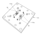
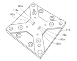
図1は、この実施形態に係る電気的接続装置の全体構成を示す斜視図である。図2は、図1のA-A矢視断面図である。図2の被検査体2のうち左側半分は被検査体2の電極端子21が電気的接触子13に接触していない状態を示しており、被検査体2の右側半分は被検査体2が押し込まれて、被検査体2の電極端子21が電気的接触子13に接触している状態を示している。図3は、上部ハウジング部111の上面構成を示す構成図であり、図4は、上部ハウジング部111の上面にフローティングガイド部113を設けた状態の構成を示す構成図であり、図5は、下部ハウジング部112の下面の構成を示す構成図である。
FIG. 1 is a perspective view showing the overall configuration of an electrical connecting device according to this embodiment. 2 is a cross-sectional view taken along the line AA in FIG. 1. FIG. The left half of the device under
図1に示すように、電気的接続装置1は、テスト基板に固定される基台11と、基台11に収容された被検査体2を固定すると共に、基台11に対して開閉自在に設けられたカバー12とを有する。
As shown in FIG. 1, the
電気的接続装置1は、例えばICパッケージ等の被検査体2の電気的特性の試験に用いられる。より具体的に、電気的接続装置1は、被検査体2としての集積回路の電気的試験(例えばパッケージテストやファイナルテスト等)に用いる試験用ICソケットとして用いられる。
The
電気的接続装置1の基台11には、被検査体2の電極端子21(第1の接触対象)と接触する複数の電気的接触子13(図2参照)が搭載されており、基台11の中央部に被検査体2が装着され、カバー12が閉状態となることで、被検査体2が押し込まれ、被検査体2の電極端子21が各電気的接触子13の先端部54に電気的接触した状態となる。そして、電気的接続装置1の基台11側が基板3上に設けられ、電気的接触子13の下端部が配線パターン31(第2の接触対象)と電気的に接触して、被検査体2の電気的特性が試験される。
A
図2に示すように、電気的接続装置1が取り付けられる基板3は、例えば電気絶縁部材で形成された配線基板である。基板3の上面には、例えば印刷配線技術により導電性を有する金属材料からなる配線パターン31が形成されている。配線パターン31は、検査装置(図示省略)の配線パターンと接続しており、配線パターン31が形成された基板3の表面上に、電気的接続装置1の基台11が固定される。
As shown in FIG. 2, the
配線パターン31は、電気的接続装置1の基台11に搭載される各電気的接触子13の位置と対応する位置に形成される。すなわち、配線パターン31は、基板3上であって、各電気的接触子13の下部アーム部135の先端部63と電気的に接続するように形成されている。
The
図2に示すように、基台11は、下部ハウジング部112と、下部ハウジング部112の上面に設けられる上部ハウジング部111と、上部ハウジング部111の中央部に設けられるフローティングガイド部113と、フレーム部114とを有する。
As shown in FIG. 2, the
フレーム部114は、電気絶縁部材で形成されており、上部ハウジング部111の上面に設けられるフローティングガイド部113の上面周縁を係止した状態で、上部ハウジング部111の上面に固定されている。
The
図4に示すように、フローティングガイド部113の中央部には、被検査体2を脱着可能に装着する凹形状の被検査体収容部113bがある。この被検査体収容部113bは、収容された被検査体2の位置決めを確実にするため、基板3に対して垂直な収容壁面を有する。また、フローティングガイド部113には、凹形状の被検査体収容部113bの両サイドには、被検査体収容部113bの凹形状と連なって形成された凹部113cがある。被検査体収容部113bの両サイドに設けられた各凹部113cの底部には、複数のスリット113aが設けられている。
As shown in FIG. 4, in the central portion of the
複数のスリット113aの下側には、電気的接触子13が配置されており、電気的接触子13の先端部54が各スリット113aから突出し、電気的接触子13の先端部54が被検査体2の電極端子21と電気的に接触する。複数のスリット113aは、被検査体2の複数の電極端子21の位置と対応する位置に配列されており、隣り合うスリット113a同士は、隔壁によって区画されている。
The
上部ハウジング部111と下部ハウジング部112とは、電気的絶縁部材で形成されており、複数の電気的接触子13を収容する部材である。より具体的には、上部ハウジング部111と下部ハウジング部112との間に複数の電気的接触子13を配列させて、複数の電気的接触子13を収容した状態で、上部ハウジング部111と下部ハウジング部112とを固定部材(例えばネジ等)で固定する。このようにして、上部ハウジング部111と下部ハウジング部112との間に複数の電気的接触子13を収容する。
The
図2に示すように、上部ハウジング部111の下面には、複数の電気的接触子13を収容するために第1の窪み部40が設けられている。さらに、上部ハウジング部111の第1の窪み部40の上面には、下方から上方に向けて設けられた穴部41及び穴部42が設けられている。
As shown in FIG. 2, the lower surface of the
穴部41と穴部42は、収容される各電気的接触子13の2つの位置決め部である第1の位置決め部132と第2の位置決め部133の位置と対応する位置にあり、各電気的接触子13が収容される際に、各電気的接触子13の2つの第1の位置決め部132と第2の位置決め部133が穴部41と穴部42とに差し込まれる。これにより、収容する各電気的接触子13の位置決めを確実にすることができ、各電気的接触子13の位置精度を高めることができる。また、各電気的接触子13の第1の位置決め部132と第2の位置決め部133を、それぞれ対応する穴部41と穴部42に差し込むだけでよいため、簡単に各電気的接触子13をセットすることができると共に、各電気的接触子13の姿勢を安定化でき、被検査体2の電極端子21と各電気的接触子13の先端部54との電気的接触を確実にすることができる。
The
なお、上部ハウジング部111の第1の窪み部40に設ける穴部41と穴部42は、上部ハウジング部111の厚さ方向に貫通していない穴部である場合を例示するが、穴部41と穴部42は、上部ハウジング部111の厚さ方向に貫通している貫通孔としてもよい。換言すると、各電気的接触子13の位置決めを確実にするために、各電気的接触子13の第1の位置決め部132と第2の位置決め部133を差し込むことができる構造であれば、穴部41と穴部42は、貫通孔であっても良いし、非貫通孔であってもよい。
Note that the
図3に示すように、上部ハウジング部111の上面には、略四角形の開口である1対の開口部111aが設けられている。各開口部111aは、被検査体2の電極端子21の位置と対応する位置に設けられ、各開口部111aの下側には、位置決めされた複数の電気的接触子13が配置されている。つまり、位置決めされた各電気的接触子13の上部アーム部134が開口部111aから突出し、その上部アーム部134の先端部54が被検査体2の電極端子21と電気的に接触する。被検査体2が押し下げられ、被検査体2の電極端子21が各電気的接触子13の先端部54に接触する際、各電気的接触子13の上部アーム部134が上下方向に弾性的に被検査体2を支持するため、上部アーム部134が変形する。このように変形した上部アーム部134と周辺部材との接触を回避するために、各開口部111aが設けられている。
As shown in FIG. 3, the top surface of the
図2に示すように、下部ハウジング部112には、厚さ方向に窪んだ第2の窪み部45が設けられている。下部ハウジング部112の上面のうち、第2の窪み部45の周囲部分は、セットされた各電気的接触子13の本体部131を下方から支持する支持部46として作用し、第2の窪み部45には、各電気的接触子13の下部アーム部135が収容される。
As shown in FIG. 2, the
つまり、下部ハウジング部112の第2の窪み部45の周囲部分である支持部46に電気的接触子13の左右端部が引っ掛かるように、電気的接触子13が置かれた状態となり、電気的接触子13が収容される。したがって、第2の窪み部45の左右方向の長さは、各電気的接触子13の本体部131の左右方向の長さよりも短くなっており、位置決めされた各電気的接触子13の両端部を、下部ハウジング部112の支持部46が支持できるようになっている。
In other words, the
下部ハウジング部112の第2の窪み部45の底部には、複数の孔部112aが設けられている。図5に示すように、複数の孔部112aから、各電気的接触子13の下部アーム部135の先端部63が突出するようになっている。各孔部112aは、基板3上の配線パターン31の位置と対応する位置に設けられており、各孔部112aから突出する各電気的接触子13の先端部63と配線パターン31とが確実に電気的に接触する。
A plurality of
[電気的接触子]
次に、図6を参照して、電気的接触子13の構成を説明する。図6は、上部ハウジング部111と下部ハウジング部112に収容される電気的接触子13の構成を示す構成図である。
[Electrical contact]
Next, referring to FIG. 6, the configuration of the
電気的接触子13は、板状の本体部131と、被検査体2の電極端子21と電気的に接触する上部アーム部134と、基板3の配線パターン31と電気的に接触する下部アーム部135と、本体部131の一方の端部(図6では、左端部)に設けられた第1の位置決め部132と、本体部131の他方の端部(図6では、右端部)側に設けられた第2の位置決め部133とを有する。
The
電気的接触子13は、例えば全体が薄い板状の導電性部材で形成されている。電気的接触子13は、全体が金属部材で形成されても良いし、基材の表面に金属材でメッキ加工されていてもよい。
The
電気的接触子13が、被検査体2側と電気的に接触する上部アーム部134と、基板3側と電気的に接触する下部アーム部135とを備え、電気的接触子13全体が、金属部材等の導電性部材で形成されることにより、被検査体2の高温環境(例えば、150℃以上の環境)での電気的試験にも対応できる。つまり、従来、エラストマ等の付勢部材を用いて、複数の電気的接触子を支持するような構造もあったが、高温環境下でこのような付勢部材を用いた場合には、付勢部材が劣化してしまい対応できないことがあったが、この実施形態の電気的接触子13とすることで、高温環境下での電気的試験にも対応できる。
The
本体部131は、板状の部材であり、上部ハウジング部111の下面に設けられた第1の窪み部40に収容される。本体部131の上下方向(高さ方向)の長さは、第1の窪み部40の上下方向(上部ハウジング部111の厚さ方向)の長さと同程度若しくはわずかに小さく形成されている。
The
第1の位置決め部132は、本体部131の一方の端部(左端部)に位置しており、本体部131の端部から垂直上方に延びた凸形状の部分である。第2の位置決め部133は、本体部131の他方の端部(右端部)から、わずかに本体部131の中央部に寄った位置にあり、垂直上方に延びた凸形状の部分である。
The
第1の位置決め部132と第2の位置決め部133の径は、穴部41と穴部42の径よりもわずかに小さく形成されており、電気的接触子13が収容される際には、第1の位置決め部132が上部ハウジング部111の穴部41に差し込まれ、第2の位置決め部133が上部ハウジング部111の穴部42に差し込まれることで、電気的接触子13の位置決めを確実にすることができる。
The diameters of the
つまり、電気的接触子13の両端部側に、2つの位置決め部として第1の位置決め部132と第2の位置決め部133とを備え、第1の位置決め部132と第2の位置決め部133とを穴部41及び穴部42に差し込むだけで、電気的接触子13の位置決めを簡単かつ確実にすることができる。
That is, a
第1の位置決め部132の下方である本体部131の下面は、下部ハウジング部112の上面である支持部46と接触して、当該支持部46により支持される第1の下部接触部138がある。また、本体部131の他方の端部の下方には、下部ハウジング部112の上面である支持部46と接触して、当該支持部46に支持される第2の下部接触部139がある。
The lower surface of the
第1の下部接触部138と第2の下部接触部139が、下部ハウジング部112の上面である支持部46に支持されることにより、収容された電気的接触子13の姿勢(収容状態)を安定して保持すると共に、精度良く位置決めされた電気的接触子13の状態を維持することができる。また、被検査体2が押し込まれ、被検査体2の電極端子21が上部アーム部134の先端部54に接触したときに、電気的接触子13には下向き荷重がかかるが、第1の下部接触部138及び第2の下部接触部139が支持部46に支持されることで、下向き荷重に対応することができる。
The first
第1の位置決め部132と上部アーム部134の上部基部51との間の本体部131の上部には、上部ハウジング部111の第1の窪み部40の下面と接触可能な第1の上部接触部136がある。また、本体部131の他方の端部(右端部)の上部には、第1の窪み部40の下面と接触可能な第2の上部接触部137がある。
A first upper contact portion capable of contacting the lower surface of the
被検査体2の押し込み荷重が電気的接触子13に生じたときに、第1の上部接触部136と第2の上部接触部137が上部ハウジング部111の上面に当たることで、電気的接触子13の浮き上がりを抑えることができる。つまり、後述するように、上部アーム部134の先端部54は、電気的接触子13の第1の位置決め部132の位置の上方に位置しているので、被検査体2の押し込み荷重が作用したときには、電気的接触子13の右側端部の浮き上がりが生じ得るが、第1の上部接触部136及び第2の上部接触部137が上部ハウジング部111の上面と当たることで、電気的接触子13の右側端部の浮き上がりを抑える。
When the pressing load of the device under
上部アーム部134は、本体部131から垂直上方に延びる上部基部51と、上部基部51から横方向(図6の右方向)に延びて円弧状に湾曲する湾曲部52と、湾曲部52から横方向(図6の左方向)に延びる支持部53と、支持部53の端部が垂直上方に向けて延びる先端部54とを有する。
The
上部アーム部134は、片持ち梁構造で形成されている。したがって、被検査体2が押しこまれ、被検査体2の電極端子21が先端部54と接触すると、先端部54が下がり、支持部53が上下方向に撓むので、上部アーム部134は上下方向に弾性を有する。これにより、被検査体2の電極端子21と先端部54とが確実に電気的接触することになる。
The
下部アーム部135は、本体部131から垂直下方に延びかつ円弧状に湾曲する下部基部61と、湾曲している下部基部61から横方向(図6の左方向)に延びる支持部62と、支持部62の端部が垂直下方に向けて延びる先端部63とを有する。
The
下部アーム部135は、片持ち梁構造で形成されている。したがって、被検査体2が押し下げられ、被検査体2が上部アーム部134と接触すると、荷重が下部アーム部135にもかかるが、支持部62が上下方向に撓むので、下部アーム部135が弾性を有する。そのため、先端部63が基板3の配線パターン31に確実に電気的に接触することになる。
The
[電気的接触子の変形例(その1)]
図7は、電気的接触子の構成の変形例(その1)を示す構成図である。
[Modified example of electrical contact (part 1)]
FIG. 7 is a configuration diagram showing a modification (part 1) of the configuration of the electrical contact.
図7に示す電気的接触子を「電気的接触子13A」と呼んで説明する。また、以下では、図7の電気的接触子13Aと、図6の電気的接触子13とを比較しながら異なる点を中心に説明する。
The electrical contact shown in FIG. 7 will be referred to as "
図7の電気的接触子13Aの基本的な構成は、図6の電気的接触子13の構成と同じであるが、図7の電気的接触子13Aの先端部54の位置が、図6の電気的接触子13の先端部54の位置と異なる。
The basic configuration of the
図6の電気的接触子13は、上部アーム部134の先端部54が、下部アーム部135の先端部63の位置よりも、左側(すなわち、被検査体2の電極端子21側)に位置している。
In the
これに対して、図7の電気的接触子13Aは、上部アーム部134の先端部54が、下部アーム部135の先端部63の位置とほぼ同じ位置に位置している。
On the other hand, in the
図6の電気的接触子13は、比較的サイズが小さい被検査体2に対応することができる。これに対して、図7の電気的接触子13は、図6の電気的接触子13が対応可能な被検査体2よりもサイズの大きい被検査体2に対応することができる。
The
被検査体2のサイズが小さい場合、被検査体収容部113bに収容される被検査体2の電極端子21の位置が、被検査体収容部113bの中央部に寄った位置にあるので、上部アーム部134の先端部54の位置を、被検査体収容部113bの中央部側(被検査体2側)に引き出すことが必要となる。したがって、図6の電気的接触子13は、上部アーム部134の位置を基台11の中央部側、すなわち本体部131の中央部よりも左側側としている。これにより、上部アーム部134の先端部54の位置が、下部アーム部135の先端部63の位置よりも左側となるようにしている。
When the size of the object to be inspected 2 is small, the position of the
これに対して、被検査体2のサイズが大きくなれば、被検査体収容部113bに主要される被検査体2の電極端子21の位置が、被検査体収容部113bの中央部よりも外側に位置することになる。したがって、図7の電気的接触子13Aは、上部アーム部134の位置を本体部131の中央部付近としているので、上部アーム部134の先端部54の位置が、下部アーム部135の先端部63の位置とほぼ同じ位置としている。
On the other hand, if the size of the object to be inspected 2 is increased, the position of the
いずれにしても、実施形態のように、上部アーム部134と下部アーム部135とを備える電気的接触子13及び13Aによれば、被検査体2の大きさに応じて、上部アーム部134の位置を調整することにより、被検査体2の電極端子21と接触する先端部54の位置を調整することができる。
In any case, according to the
なお、図6及び図7では、被検査体2の電極端子21と電気的に接触させる上部アーム部134の先端部54の位置を調整する場合を例示したが、下部アーム部135の位置についても調整するようにしてもよい。
6 and 7 illustrate the case of adjusting the position of the
[電気的接触子の変形例(その2)]
図8は、電気的接触子の構成の変形例(その2)を示す構成図である。
[Modified example of electrical contact (Part 2)]
FIG. 8 is a configuration diagram showing a modification (No. 2) of the configuration of the electrical contact.
図8に示す電気的接触子を「電気的接触子13B」と呼んで説明する。また、以下では、図8の電気的接触子13Bと、図6及び図7の電気的接触子13及び13Aとを比較しながら異なる点を中心に説明する。
The electrical contact shown in FIG. 8 will be referred to as "
図8の電気的接触子13Bの上部アーム部134Bが、本体部131の垂直上方に延びる上部基部55と、上部基部55から円弧状に湾曲して横方向(図8の左方向)に延びる支持部53と、支持部53の端部が垂直上方に向けて延びる先端部54とを有する。
The
図8の電気的接触子13Bは、上部アーム部134の先端部54の位置を、図6の電気的接触子13の先端部54の位置よりも、更に被検査体収容部113bの中央部側に位置させることができる。換言すると、図8の電気的接触子13Bは、図6の電気的接触子13が対応可能なサイズの被検査体2よりも、さらに小さなサイズの被検査体2にも対応することができる。
The
また、図8の電気的接触子13Bは、上部アーム部134Bが、本体部131に対して垂直上方に延びる上部基部55と、支持部53と、支持部53に対して垂直上方に延びる先端部54とからなるので、スリット113aから突出させる先端部54の位置精度がより向上する。つまり、スリット113aから突出する先端部54の位置精度が高くあり、かつ、被検査体2の電極端子21が先端部54に接触すると、先端部54が垂直下方にまっすぐ下がるので、被検査体2の電極端子21に接触させる電気的接触子13Bの先端部54の位置精度が確実になる。
8, the
(A-2)実施形態の効果
以上のように、この実施形態によれば、電気的接触子が、被検査体側と電気的に接触させる片持ち梁構造の上部アーム部と、基板端子側と電気的に接触させる片持ち梁構造の下部アーム部とを有する構造としたことで、高温環境下での被検査体の電気的試験に対応することができる。
(A-2) Effect of the Embodiment As described above, according to this embodiment, the electrical contact is provided with the upper arm portion of the cantilever structure for making electrical contact with the device under test and the substrate terminal side. By adopting the structure having the lower arm portion of the cantilever structure to be electrically contacted, it is possible to cope with the electrical test of the device under test in a high-temperature environment.
また、この実施形態によれば、導電性部材を加工して、片持ち梁構造の上部アーム部と片持ち梁構造の下部アーム部とを有する電気的接触子とすることで、上部アーム部と被検査体の電極端子の接触抵抗、下部アーム部と基板端子との接触抵抗を安定化させることができる。 Further, according to this embodiment, by processing the conductive member to form an electrical contact having an upper arm portion with a cantilever structure and a lower arm portion with a cantilever structure, the upper arm portion and the The contact resistance of the electrode terminals of the device under test and the contact resistance between the lower arm portion and the substrate terminals can be stabilized.
さらに、この実施形態によれば、電気的接触子が2つの位置決め部を備えることとしたので、被検査体の電極端子に対する先端部の位置決め精度を高めることができる。その結果、被検査体の電極端子と電気的接触子の先端部との電気的接触を確実にすることができる。 Furthermore, according to this embodiment, the electrical contact has two positioning portions, so that the positioning accuracy of the tip portion with respect to the electrode terminal of the device under test can be improved. As a result, electrical contact between the electrode terminal of the device under test and the tip of the electrical contactor can be ensured.
(B)他の実施形態
上述した実施形態においても種々の変形実施形態を言及したが、本発明は、以下の変形実施形態にも適用できる。
(B) Other Embodiments Although various modified embodiments have been mentioned in the embodiments described above, the present invention can also be applied to the following modified embodiments.
図9は、変形実施形態に係る電気的接触子の構成を示す構成図である。 FIG. 9 is a configuration diagram showing the configuration of an electrical contact according to a modified embodiment.
図9において、変形実施形態の電気的接触子13Cは、2個の電気的接触子13と、2個の電気的接触子13の間に設けた絶縁部材7とを有する。
In FIG. 9, an
絶縁部材7は、例えば絶縁性のフィルム、板状の絶縁部材等を用いることができる。絶縁部材7の形状は、電気的接触子13の形状に応じて適宜設計することができるが、例えば図9の場合、2個の電気的接触子13の本体部131、上部アーム部134、下部アーム部135との間で導通しないような形状とする。
For example, an insulating film, a plate-like insulating member, or the like can be used as the insulating
2個の電気的接触子13はそれぞれ、図6の電気的接触子13と同じ構造である。2個の電気的接触子13のうち、一方の電気的接触子13と、他方の電気的接触子13との間に、絶縁部材7を挟み込んだ構造としている。つまり、2個の電気的接触子13の間に絶縁部材7を挟み込むことで、2個の電気的接触子13はそれぞれ互いに導通しないようにしている。
Each of the two
これにより、例えば、被検査体2について4端子測定(例えばケルビン接続測定)を行なう場合に、被検査体2が4端子測定用の各電極端子21に、電気的接触子13Cを構成する各電気的接触子13の上部アーム部134の先端部54を接触させて測定することができる。
As a result, for example, when the device under
なお、図9では、図6の電気的接触子13を用いた場合を例示しているが、これら電気的接触子13に代えて、図7の電気的接触子13A、図8の電気的接触子13Bを用いるようにしてもよい。
9 exemplifies a case where the
図9のような電気的接触子13Cの構造とすることで、被検査体2のケルビン測定の際に電気的接触子13Cを用いることができる。
By configuring the
1…電気的接続装置、11…基台、12…カバー、111…上部ハウジング部、111a…開口部、112…下部ハウジング部、112a…孔部、113…フローティングガイド部、113a…スリット、113b…被検査体収容部、113c…凹部、114…フレーム部、
13、13A、13B及び13C…電気的接触子、131…本体部、132…第1の位置決め部、133…第2の位置決め部、134、134A及び134B…上部アーム部、135…下部アーム部、136…第1の上部接触部、137…第2の上部接触部、138…第1の下部接触部、139…第2の下部接触部、
51及び55…上部基部、52…湾曲部、53…支持部、54…先端部、61…下部基部、62…支持部、63…先端部、
2…被検査体、21…電極端子、3…基板、31…配線パターン、
40…第1の窪み部、41…穴部、42…穴部、45…第2の窪み部、46…支持部、7…絶縁部材。
DESCRIPTION OF
13, 13A, 13B and 13C...
51 and 55... Upper base, 52... Curved part, 53... Support part, 54... Tip part, 61... Lower base part, 62... Support part, 63... Tip part,
2... Object to be inspected, 21... Electrode terminal, 3... Substrate, 31... Wiring pattern,
40... First hollow portion, 41... Hole portion, 42... Hole portion, 45... Second hollow portion, 46... Support portion, 7... Insulating member.
Claims (6)
前記ハウジングの前記下側部材上に載置され、導電部材で形成された板状の本体部と、
前記本体部から一体的に連続して上方に延出した上部基部と、前記上部基部から前記本体部に沿って横方向に延出した上部支持部と、前記上部支持部から垂直上方に延出して第1の接触対象と電気的に接触する第1の先端部とを有する片持ち梁構造の上部アーム部と、
前記本体部から一体的に連続して下方に延出した下部基部と、前記下部基部から前記本体部に沿って横方向に延出した下部支持部と、前記下部支持部から垂直下方に延出して第2の接触対象と電気的に接触する第2の先端部とを有する片持ち梁構造の下部アーム部と、
前記本体部の一方の端部から上方に延出した第1の位置決め部と、
前記本体部の他方の端部付近から上方に延出した第2の位置決め部と
を備え、
前記上部アーム部は、前記ハウジングの前記上側部材に設けられた上下方向に貫通する開口部を通って配置し、
前記下部アーム部は、前記ハウジングの前記下側部材に設けられた上下方向に貫通する開口部を通って配置し、
前記第1の位置決め部が、前記ハウジングの前記上側部材の下面に設けられた第1の穴部に収納され、
前記第2の位置決め部が、前記ハウジングの前記上側部材の下面に設けられた第2の穴部に収容される
ことを特徴とする電気的接触子。 An electrical contact that is housed and used in a housing composed of an upper member and a lower member,
a plate-like main body portion placed on the lower member of the housing and formed of a conductive member;
An upper base extending upward from the main body, an upper support extending laterally from the upper base along the main body, and extending vertically upward from the upper support. an upper arm portion of a cantilever structure having a first distal end portion electrically contacting the first contact target;
A lower base extending downward from the main body, a lower support extending laterally from the lower base along the main body, and extending vertically downward from the lower support. a cantilever structure lower arm portion having a second distal end portion electrically contacting the second contact target;
a first positioning portion extending upward from one end of the main body;
a second positioning portion extending upward from the vicinity of the other end of the main body,
the upper arm portion is disposed through an opening extending vertically through the upper member of the housing;
the lower arm portion is disposed through an opening extending vertically through the lower member of the housing;
the first positioning portion is accommodated in a first hole provided in the lower surface of the upper member of the housing;
The electrical contact, wherein the second positioning portion is accommodated in a second hole provided in the lower surface of the upper member of the housing.
前記下部アーム部は、前記下部基部が前記本体部の長手方向の中央部よりも前記他方の端部側に設けられ、前記下部基部が前記本体部から下方に延びその後湾曲して、前記下部支持部が前記下部基部から前記一方の端部に向けて延びており、
前記上部アーム部の前記第1の先端部が、前記下部アーム部の前記第2の先端部の位置よりも前記一方の端部側に位置している
ことを特徴とする請求項1に記載の電気的接触子。 In the upper arm portion, the upper base portion is provided closer to the one end than the central portion in the longitudinal direction of the main body portion, the upper base portion extends upward from the main body portion, and the upper support portion extends from the upper portion . extending from the base toward the other end, then curved in an arc shape, and extending toward the one end along the main body;
In the lower arm portion, the lower base portion is provided closer to the other end portion side than the central portion in the longitudinal direction of the main body portion, and the lower base portion extends downward from the main body portion and then bends to support the lower portion. a portion extending from the lower base toward the one end;
2. The apparatus according to claim 1, wherein the first tip portion of the upper arm portion is positioned closer to the one end portion than the second tip portion of the lower arm portion is positioned. electrical contacts.
前記下部アーム部は、前記下部基部が前記本体部の長手方向の中央部よりも前記他方の端部側に設けられ、前記下部基部が前記本体部から下方に延びその後湾曲して、前記下部支持部が前記下部基部から前記一方の端部に向けて延びており、
前記上部アーム部の前記第1の先端部が、前記下部アーム部の前記第2の先端部の位置の上方に位置している
ことを特徴とする請求項1に記載の電気的接触子。 The upper arm portion has the upper base portion provided near the center portion in the longitudinal direction of the main body portion, the upper base portion extending upward from the main body portion, and the upper support portion extending from the upper base portion to the other end portion. and then arcuately curved to extend along the main body toward the one end,
In the lower arm portion, the lower base portion is provided closer to the other end portion side than the central portion in the longitudinal direction of the main body portion, and the lower base portion extends downward from the main body portion and then bends to support the lower portion. a portion extending from the lower base toward the one end;
2. The electrical contact according to claim 1, wherein said first end portion of said upper arm portion is positioned above said second end portion of said lower arm portion.
前記下部アーム部は、前記下部基部が前記本体部の長手方向の中央部よりも前記他方の端部側に設けられ、前記下部基部が前記本体部から下方に延びその後湾曲して、前記下部支持部が前記下部基部から前記一方の端部に向けて延びており、
前記上部アーム部の前記第1の先端部が、前記本体部の前記一方の端部に設けた前記第1の位置決め部の位置よりも外側に位置している
ことを特徴とする請求項1に記載の電気的接触子。 In the upper arm portion, the upper base portion is provided closer to the one end than the central portion in the longitudinal direction of the main body portion, the upper base portion extends upward from the main body portion, and the upper support portion extends from the upper portion . extending from the base toward the other end, then curved in an arc shape, and extending toward the one end along the main body;
In the lower arm portion, the lower base portion is provided closer to the other end portion side than the central portion in the longitudinal direction of the main body portion, and the lower base portion extends downward from the main body portion and then bends to support the lower portion. a portion extending from the lower base toward the one end;
2. The apparatus according to claim 1, wherein the first tip portion of the upper arm portion is positioned outside the position of the first positioning portion provided at the one end portion of the main body portion. Electrical contacts as described.
前記複数の電気的接触子の間に挟まれた絶縁部材と
を備えることを特徴とする電気的接触子。 An electrical contact comprising: a plurality of electrical contacts according to any one of claims 1 to 4; and an insulating member sandwiched between the plurality of electrical contacts.
前記ハウジング部が、前記複数の電気的接触子を収容する収容内部の上面に、前記各電気的接触子の一方の端部にある第1の位置決め部を収容する第1の穴部と、前記各電気的接触子の他方の端部側にある第2の位置決め部を収容する第2の穴部とを備えることを特徴とする電気的接続装置。 A substrate on which wiring is formed, a housing portion accommodating the plurality of electrical contacts according to any one of claims 1 to 5 on the substrate, and the plurality of electrical contacts accommodated in the housing portion. and an object-to-be-tested accommodation portion for accommodating an object-to-be-inspected at a position that can be contacted with the electrical contact between the electrode portion of the object-to-be-tested and the wiring of the substrate. In the electrical connection device to be connected to
a first hole portion for accommodating a first positioning portion at one end of each of the electrical contacts; and a second hole accommodating a second positioning portion on the other end side of each electrical contact.
Priority Applications (4)
| Application Number | Priority Date | Filing Date | Title |
|---|---|---|---|
| JP2019072224A JP7301582B2 (en) | 2019-04-04 | 2019-04-04 | Electrical contacts and electrical connecting devices |
| US16/784,847 US11340289B2 (en) | 2019-04-04 | 2020-02-07 | Electrical contactor and electrical connecting apparatus |
| CN202010257225.0A CN111796124A (en) | 2019-04-04 | 2020-04-03 | Electrical contact and electrical connection device |
| PH12020050163A PH12020050163A1 (en) | 2019-04-04 | 2020-05-25 | Electrical contactor and electrical connecting apparatus |
Applications Claiming Priority (1)
| Application Number | Priority Date | Filing Date | Title |
|---|---|---|---|
| JP2019072224A JP7301582B2 (en) | 2019-04-04 | 2019-04-04 | Electrical contacts and electrical connecting devices |
Publications (3)
| Publication Number | Publication Date |
|---|---|
| JP2020169928A JP2020169928A (en) | 2020-10-15 |
| JP2020169928A5 JP2020169928A5 (en) | 2022-03-22 |
| JP7301582B2 true JP7301582B2 (en) | 2023-07-03 |
Family
ID=72662250
Family Applications (1)
| Application Number | Title | Priority Date | Filing Date |
|---|---|---|---|
| JP2019072224A Active JP7301582B2 (en) | 2019-04-04 | 2019-04-04 | Electrical contacts and electrical connecting devices |
Country Status (4)
| Country | Link |
|---|---|
| US (1) | US11340289B2 (en) |
| JP (1) | JP7301582B2 (en) |
| CN (1) | CN111796124A (en) |
| PH (1) | PH12020050163A1 (en) |
Families Citing this family (1)
| Publication number | Priority date | Publication date | Assignee | Title |
|---|---|---|---|---|
| JP2022045105A (en) * | 2020-09-08 | 2022-03-18 | 山一電機株式会社 | Examination kelvin contact, examination kelvin socket, and method for manufacturing examination kelvin contact |
Citations (4)
| Publication number | Priority date | Publication date | Assignee | Title |
|---|---|---|---|---|
| JP2002365308A (en) | 2001-06-08 | 2002-12-18 | Japan Electronic Materials Corp | Vertical blade type probe, vertical blade type probe unit and vertical blade type probe card using the same |
| JP2005141986A (en) | 2003-11-05 | 2005-06-02 | Yamaichi Electronics Co Ltd | Socket for semiconductor device |
| JP2010008388A (en) | 2008-06-30 | 2010-01-14 | Rika Denshi Co Ltd | Ic socket |
| JP2011153998A (en) | 2010-01-28 | 2011-08-11 | Nhk Spring Co Ltd | Contact probe and probe unit |
Family Cites Families (17)
| Publication number | Priority date | Publication date | Assignee | Title |
|---|---|---|---|---|
| JP3094007B2 (en) * | 1998-06-02 | 2000-10-03 | 日本電子材料株式会社 | Probe and probe card using this probe |
| JP3810977B2 (en) * | 2000-02-25 | 2006-08-16 | 株式会社エンプラス | Socket for electrical parts |
| US7265565B2 (en) * | 2003-02-04 | 2007-09-04 | Microfabrica Inc. | Cantilever microprobes for contacting electronic components and methods for making such probes |
| JP2004117081A (en) * | 2002-09-25 | 2004-04-15 | Japan Electronic Materials Corp | Vertical-type probe unit and vertical-type probe card using the same |
| SG118181A1 (en) * | 2003-03-25 | 2006-01-27 | Fci Asia Technology Pte Ltd | High density electrical connector |
| US7192320B2 (en) * | 2004-03-26 | 2007-03-20 | Silicon Pipe, Inc. | Electrical interconnection devices incorporating redundant contact points for reducing capacitive stubs and improved signal integrity |
| WO2006003722A1 (en) * | 2004-07-05 | 2006-01-12 | Kabushiki Kaisha Nihon Micronics | Contact block and electrical connection device |
| JP2006162422A (en) * | 2004-12-07 | 2006-06-22 | Japan Electronic Materials Corp | Probe card |
| JP2006337080A (en) * | 2005-05-31 | 2006-12-14 | Micronics Japan Co Ltd | Probe for current test |
| JP5123489B2 (en) * | 2006-04-07 | 2013-01-23 | 株式会社日本マイクロニクス | Electrical connection device |
| US9329204B2 (en) * | 2009-04-21 | 2016-05-03 | Johnstech International Corporation | Electrically conductive Kelvin contacts for microcircuit tester |
| SG195107A1 (en) | 2011-05-27 | 2013-12-30 | Jf Microtechnology Sdn Bhd | An electrical interconnect assembly |
| JP5429308B2 (en) * | 2011-07-11 | 2014-02-26 | 株式会社デンソー | Electronic equipment |
| JP2013171685A (en) * | 2012-02-20 | 2013-09-02 | Molex Inc | Connector |
| US9281577B2 (en) * | 2013-12-30 | 2016-03-08 | Lennox Industries Inc. | Control signal routing apparatus |
| MY191065A (en) * | 2016-06-28 | 2022-05-30 | Nihon Micronics Kk | Electrical connecting apparatus and contact |
| KR101683070B1 (en) * | 2016-09-27 | 2016-12-06 | 주식회사 제이앤에프이 | Face- front socket for testing of camera module |
-
2019
- 2019-04-04 JP JP2019072224A patent/JP7301582B2/en active Active
-
2020
- 2020-02-07 US US16/784,847 patent/US11340289B2/en active Active
- 2020-04-03 CN CN202010257225.0A patent/CN111796124A/en active Pending
- 2020-05-25 PH PH12020050163A patent/PH12020050163A1/en unknown
Patent Citations (4)
| Publication number | Priority date | Publication date | Assignee | Title |
|---|---|---|---|---|
| JP2002365308A (en) | 2001-06-08 | 2002-12-18 | Japan Electronic Materials Corp | Vertical blade type probe, vertical blade type probe unit and vertical blade type probe card using the same |
| JP2005141986A (en) | 2003-11-05 | 2005-06-02 | Yamaichi Electronics Co Ltd | Socket for semiconductor device |
| JP2010008388A (en) | 2008-06-30 | 2010-01-14 | Rika Denshi Co Ltd | Ic socket |
| JP2011153998A (en) | 2010-01-28 | 2011-08-11 | Nhk Spring Co Ltd | Contact probe and probe unit |
Also Published As
| Publication number | Publication date |
|---|---|
| CN111796124A (en) | 2020-10-20 |
| PH12020050163A1 (en) | 2021-06-14 |
| US11340289B2 (en) | 2022-05-24 |
| US20200319245A1 (en) | 2020-10-08 |
| JP2020169928A (en) | 2020-10-15 |
Similar Documents
| Publication | Publication Date | Title |
|---|---|---|
| US6575767B2 (en) | Contact pin assembly, contact pin assembly manufacturing method, contact pin assembling structure, contact pin assembling structure manufacturing method, and socket for electrical parts | |
| KR20020096892A (en) | Socket for electricparts | |
| JP7301582B2 (en) | Electrical contacts and electrical connecting devices | |
| JP5079806B2 (en) | Inspection structure | |
| US20050136704A1 (en) | Die carrier | |
| TWI801754B (en) | Electrical contact, electrical connection structure and electrical connection device | |
| JP2015060622A (en) | Contact pin and electric component socket | |
| US7121860B2 (en) | Pinch-style support contact, method of enabling electrical communication with and supporting an IC package, and socket including same | |
| KR20100098584A (en) | Test socket for semiconductor chip | |
| JP4213455B2 (en) | Socket for electrical parts | |
| JP2008076268A (en) | Inspection tool | |
| KR101446146B1 (en) | A Testing Device | |
| JP2002270320A (en) | Socket for semiconductor package | |
| JP2004235591A (en) | Electric connection device | |
| JP2004085261A (en) | Probe pin and contactor | |
| JPH07111176A (en) | Connector inspection jig | |
| JP6039425B2 (en) | Inspection system | |
| JP2004138576A (en) | Electrical connection device | |
| JP7374037B2 (en) | pogo block | |
| JP2020169928A5 (en) | ||
| JP2020017713A (en) | Intermediate connecting member and inspection device | |
| KR102456348B1 (en) | Interposer and test socket having the same | |
| JP7309219B2 (en) | Probe terminals, evaluation sockets, and device evaluation methods | |
| KR20230152991A (en) | Interposer and test socket having the same | |
| KR20240056419A (en) | Electrical contactor, electrical connecting structure and electrical connecting apparatus |
Legal Events
| Date | Code | Title | Description |
|---|---|---|---|
| A521 | Request for written amendment filed |
Free format text: JAPANESE INTERMEDIATE CODE: A523 Effective date: 20220311 |
|
| A621 | Written request for application examination |
Free format text: JAPANESE INTERMEDIATE CODE: A621 Effective date: 20220311 |
|
| A977 | Report on retrieval |
Free format text: JAPANESE INTERMEDIATE CODE: A971007 Effective date: 20221031 |
|
| A131 | Notification of reasons for refusal |
Free format text: JAPANESE INTERMEDIATE CODE: A131 Effective date: 20221108 |
|
| A521 | Request for written amendment filed |
Free format text: JAPANESE INTERMEDIATE CODE: A523 Effective date: 20221215 |
|
| A131 | Notification of reasons for refusal |
Free format text: JAPANESE INTERMEDIATE CODE: A131 Effective date: 20230328 |
|
| A521 | Request for written amendment filed |
Free format text: JAPANESE INTERMEDIATE CODE: A523 Effective date: 20230404 |
|
| TRDD | Decision of grant or rejection written | ||
| A01 | Written decision to grant a patent or to grant a registration (utility model) |
Free format text: JAPANESE INTERMEDIATE CODE: A01 Effective date: 20230523 |
|
| A61 | First payment of annual fees (during grant procedure) |
Free format text: JAPANESE INTERMEDIATE CODE: A61 Effective date: 20230621 |
|
| R150 | Certificate of patent or registration of utility model |
Ref document number: 7301582 Country of ref document: JP Free format text: JAPANESE INTERMEDIATE CODE: R150 |