JP7296090B2 - Flash modules and terminals containing them - Google Patents
Flash modules and terminals containing them Download PDFInfo
- Publication number
- JP7296090B2 JP7296090B2 JP2018560764A JP2018560764A JP7296090B2 JP 7296090 B2 JP7296090 B2 JP 7296090B2 JP 2018560764 A JP2018560764 A JP 2018560764A JP 2018560764 A JP2018560764 A JP 2018560764A JP 7296090 B2 JP7296090 B2 JP 7296090B2
- Authority
- JP
- Japan
- Prior art keywords
- light emitting
- light
- flash module
- wavelength
- lens
- Prior art date
- Legal status (The legal status is an assumption and is not a legal conclusion. Google has not performed a legal analysis and makes no representation as to the accuracy of the status listed.)
- Active
Links
Images


Classifications
-
- G—PHYSICS
- G03—PHOTOGRAPHY; CINEMATOGRAPHY; ANALOGOUS TECHNIQUES USING WAVES OTHER THAN OPTICAL WAVES; ELECTROGRAPHY; HOLOGRAPHY
- G03B—APPARATUS OR ARRANGEMENTS FOR TAKING PHOTOGRAPHS OR FOR PROJECTING OR VIEWING THEM; APPARATUS OR ARRANGEMENTS EMPLOYING ANALOGOUS TECHNIQUES USING WAVES OTHER THAN OPTICAL WAVES; ACCESSORIES THEREFOR
- G03B15/00—Special procedures for taking photographs; Apparatus therefor
- G03B15/02—Illuminating scene
- G03B15/03—Combinations of cameras with lighting apparatus; Flash units
-
- G—PHYSICS
- G02—OPTICS
- G02B—OPTICAL ELEMENTS, SYSTEMS OR APPARATUS
- G02B5/00—Optical elements other than lenses
- G02B5/02—Diffusing elements; Afocal elements
-
- G—PHYSICS
- G03—PHOTOGRAPHY; CINEMATOGRAPHY; ANALOGOUS TECHNIQUES USING WAVES OTHER THAN OPTICAL WAVES; ELECTROGRAPHY; HOLOGRAPHY
- G03B—APPARATUS OR ARRANGEMENTS FOR TAKING PHOTOGRAPHS OR FOR PROJECTING OR VIEWING THEM; APPARATUS OR ARRANGEMENTS EMPLOYING ANALOGOUS TECHNIQUES USING WAVES OTHER THAN OPTICAL WAVES; ACCESSORIES THEREFOR
- G03B15/00—Special procedures for taking photographs; Apparatus therefor
- G03B15/02—Illuminating scene
- G03B15/03—Combinations of cameras with lighting apparatus; Flash units
- G03B15/04—Combinations of cameras with non-electronic flash apparatus; Non-electronic flash units
- G03B15/0442—Constructional details of the flash apparatus; Arrangement of lamps, reflectors, or the like
-
- G—PHYSICS
- G03—PHOTOGRAPHY; CINEMATOGRAPHY; ANALOGOUS TECHNIQUES USING WAVES OTHER THAN OPTICAL WAVES; ELECTROGRAPHY; HOLOGRAPHY
- G03B—APPARATUS OR ARRANGEMENTS FOR TAKING PHOTOGRAPHS OR FOR PROJECTING OR VIEWING THEM; APPARATUS OR ARRANGEMENTS EMPLOYING ANALOGOUS TECHNIQUES USING WAVES OTHER THAN OPTICAL WAVES; ACCESSORIES THEREFOR
- G03B15/00—Special procedures for taking photographs; Apparatus therefor
- G03B15/02—Illuminating scene
- G03B15/03—Combinations of cameras with lighting apparatus; Flash units
- G03B15/05—Combinations of cameras with electronic flash apparatus; Electronic flash units
-
- G—PHYSICS
- G03—PHOTOGRAPHY; CINEMATOGRAPHY; ANALOGOUS TECHNIQUES USING WAVES OTHER THAN OPTICAL WAVES; ELECTROGRAPHY; HOLOGRAPHY
- G03B—APPARATUS OR ARRANGEMENTS FOR TAKING PHOTOGRAPHS OR FOR PROJECTING OR VIEWING THEM; APPARATUS OR ARRANGEMENTS EMPLOYING ANALOGOUS TECHNIQUES USING WAVES OTHER THAN OPTICAL WAVES; ACCESSORIES THEREFOR
- G03B17/00—Details of cameras or camera bodies; Accessories therefor
- G03B17/56—Accessories
- G03B17/565—Optical accessories, e.g. converters for close-up photography, tele-convertors, wide-angle convertors
-
- H—ELECTRICITY
- H01—ELECTRIC ELEMENTS
- H01L—SEMICONDUCTOR DEVICES NOT COVERED BY CLASS H10
- H01L33/00—Semiconductor devices with at least one potential-jump barrier or surface barrier specially adapted for light emission; Processes or apparatus specially adapted for the manufacture or treatment thereof or of parts thereof; Details thereof
- H01L33/48—Semiconductor devices with at least one potential-jump barrier or surface barrier specially adapted for light emission; Processes or apparatus specially adapted for the manufacture or treatment thereof or of parts thereof; Details thereof characterised by the semiconductor body packages
- H01L33/50—Wavelength conversion elements
- H01L33/501—Wavelength conversion elements characterised by the materials, e.g. binder
- H01L33/502—Wavelength conversion materials
- H01L33/504—Elements with two or more wavelength conversion materials
-
- H—ELECTRICITY
- H01—ELECTRIC ELEMENTS
- H01L—SEMICONDUCTOR DEVICES NOT COVERED BY CLASS H10
- H01L33/00—Semiconductor devices with at least one potential-jump barrier or surface barrier specially adapted for light emission; Processes or apparatus specially adapted for the manufacture or treatment thereof or of parts thereof; Details thereof
- H01L33/48—Semiconductor devices with at least one potential-jump barrier or surface barrier specially adapted for light emission; Processes or apparatus specially adapted for the manufacture or treatment thereof or of parts thereof; Details thereof characterised by the semiconductor body packages
- H01L33/50—Wavelength conversion elements
- H01L33/505—Wavelength conversion elements characterised by the shape, e.g. plate or foil
-
- H—ELECTRICITY
- H01—ELECTRIC ELEMENTS
- H01L—SEMICONDUCTOR DEVICES NOT COVERED BY CLASS H10
- H01L33/00—Semiconductor devices with at least one potential-jump barrier or surface barrier specially adapted for light emission; Processes or apparatus specially adapted for the manufacture or treatment thereof or of parts thereof; Details thereof
- H01L33/48—Semiconductor devices with at least one potential-jump barrier or surface barrier specially adapted for light emission; Processes or apparatus specially adapted for the manufacture or treatment thereof or of parts thereof; Details thereof characterised by the semiconductor body packages
- H01L33/58—Optical field-shaping elements
-
- H—ELECTRICITY
- H01—ELECTRIC ELEMENTS
- H01S—DEVICES USING THE PROCESS OF LIGHT AMPLIFICATION BY STIMULATED EMISSION OF RADIATION [LASER] TO AMPLIFY OR GENERATE LIGHT; DEVICES USING STIMULATED EMISSION OF ELECTROMAGNETIC RADIATION IN WAVE RANGES OTHER THAN OPTICAL
- H01S5/00—Semiconductor lasers
- H01S5/30—Structure or shape of the active region; Materials used for the active region
- H01S5/32—Structure or shape of the active region; Materials used for the active region comprising PN junctions, e.g. hetero- or double- heterostructures
- H01S5/323—Structure or shape of the active region; Materials used for the active region comprising PN junctions, e.g. hetero- or double- heterostructures in AIIIBV compounds, e.g. AlGaAs-laser, InP-based laser
- H01S5/32308—Structure or shape of the active region; Materials used for the active region comprising PN junctions, e.g. hetero- or double- heterostructures in AIIIBV compounds, e.g. AlGaAs-laser, InP-based laser emitting light at a wavelength less than 900 nm
-
- G—PHYSICS
- G03—PHOTOGRAPHY; CINEMATOGRAPHY; ANALOGOUS TECHNIQUES USING WAVES OTHER THAN OPTICAL WAVES; ELECTROGRAPHY; HOLOGRAPHY
- G03B—APPARATUS OR ARRANGEMENTS FOR TAKING PHOTOGRAPHS OR FOR PROJECTING OR VIEWING THEM; APPARATUS OR ARRANGEMENTS EMPLOYING ANALOGOUS TECHNIQUES USING WAVES OTHER THAN OPTICAL WAVES; ACCESSORIES THEREFOR
- G03B2215/00—Special procedures for taking photographs; Apparatus therefor
- G03B2215/05—Combinations of cameras with electronic flash units
- G03B2215/0514—Separate unit
- G03B2215/0517—Housing
- G03B2215/0546—Housing modular
-
- G—PHYSICS
- G03—PHOTOGRAPHY; CINEMATOGRAPHY; ANALOGOUS TECHNIQUES USING WAVES OTHER THAN OPTICAL WAVES; ELECTROGRAPHY; HOLOGRAPHY
- G03B—APPARATUS OR ARRANGEMENTS FOR TAKING PHOTOGRAPHS OR FOR PROJECTING OR VIEWING THEM; APPARATUS OR ARRANGEMENTS EMPLOYING ANALOGOUS TECHNIQUES USING WAVES OTHER THAN OPTICAL WAVES; ACCESSORIES THEREFOR
- G03B2215/00—Special procedures for taking photographs; Apparatus therefor
- G03B2215/05—Combinations of cameras with electronic flash units
- G03B2215/0564—Combinations of cameras with electronic flash units characterised by the type of light source
- G03B2215/0567—Solid-state light source, e.g. LED, laser
Description
本発明は、カメラフラッシュ及びこれを含む端末機に関するものである。 The present invention relates to a camera flash and a terminal including the same.
GaN、AlGaN等の化合物を含む半導体素子は、広くて調整が容易なバンドギャップエネルギーを有する等多様な長所を有することから、発光素子、受光素子及び各種ダイオード等に多様に用いられている。 Semiconductor devices containing compounds such as GaN and AlGaN have various advantages such as a wide and easily adjustable bandgap energy, and are therefore widely used in light emitting devices, light receiving devices, and various diodes.
特に、半導体のIII-V族またはII-VI族化合物半導体物質を利用した発光ダイオード(Light Emitting Diode)やレーザダイオード(Laser Diode)のような発光素子は、薄膜成長技術及び素子材料の開発によって、赤色、緑色、青色及び紫外線等多様な色を具現することができ、蛍光物質を利用したり色を組合せることで、効率の良い白色光線も具現が可能であり、蛍光灯、白熱灯等既存の光源に比べて、低消費電力、半永久的な寿命、速い応答速度、安全性、環境親和性の長所を有する。 In particular, light-emitting devices such as light-emitting diodes and laser diodes using group III-V or group II-VI compound semiconductor materials of semiconductors have been developed through the development of thin film growth technology and device materials. Various colors such as red, green, blue, and ultraviolet can be realized, and efficient white light can be realized by using fluorescent materials or combining colors, and existing fluorescent lamps, incandescent lamps, etc. It has the advantages of low power consumption, semi-permanent life, fast response speed, safety and environmental friendliness compared to other light sources.
さらに、光検出器や太陽電池のような受光素子も、半導体のIII-V族またはII-VI族化合物半導体物質を利用して製作する場合、素子材料の開発によって多様な波長領域の光を吸収して光電流を生成することで、ガンマ線からラジオ波長領域まで多様な波長領域の光を利用することができる。また、速い応答速度、安全性、環境親和性及び素子材料の容易な調節といった長所を有するので、電力制御または超高周波回路や通信用モジュールにも容易に利用することができる。 In addition, light receiving devices such as photodetectors and solar cells can absorb light in various wavelength regions by developing device materials when they are manufactured using semiconductor materials of Group III-V or Group II-VI compounds. By generating a photocurrent as a photocurrent, it is possible to use light in various wavelength ranges from gamma rays to the radio wavelength range. In addition, since it has advantages such as fast response speed, safety, environmental friendliness, and easy adjustment of device materials, it can be easily applied to power control, ultra-high frequency circuits, and communication modules.
従って、光通信手段の送信モジュール、LCD(Liquid Crystal Display)表示装置のバックライトを構成する冷陰極管(CCFL:Cold Cathode Fluorescence Lamp)を代替できる発光ダイオードバックライト、蛍光灯や白熱電球を代替できる白色発光ダイオード照明装置、自動車ヘッドライト及び信号灯及びガスや火災を感知するセンサ等にまで応用が広がっている。また、高周波応用回路やその他電力制御装置、通信用モジュールにまで応用を拡大することができる。 Therefore, it can replace the transmission module of the optical communication means, the LED backlight that can replace the CCFL (Cold Cathode Fluorescence Lamp) constituting the backlight of the LCD (Liquid Crystal Display) display device, and the fluorescent lamp and the incandescent lamp. Applications include white light emitting diode lighting devices, automobile headlights, signal lights, and sensors for detecting gas and fire. In addition, applications can be expanded to high-frequency application circuits, other power control devices, and communication modules.
最近では、カメラ機能が一緒に提供される携帯用端末機が増えている。このような携帯用端末機には、カメラ撮影時に必要とする光量を提供するために、フラッシュ(Flash)が内蔵されている。これに関して、カメラフラッシュの光源として、半導体素子、例えば白色LED(Light Emitting Diode:発光ダイオード)の使用が増加している。 Recently, more and more portable terminals are provided with a camera function. Such portable terminals have built-in flashes to provide the amount of light required for camera photography. In this regard, semiconductor devices such as white LEDs (Light Emitting Diodes) are increasingly being used as light sources for camera flashes.
一方、発光素子を利用して白色光を具現する方法としては、単一チップ(Single chip)を活用する方法と、マルチチップ(Multi chip)を活用する方法がある。 On the other hand, as a method of realizing white light using a light emitting device, there are a method of using a single chip and a method of using a multi chip.
例えば、単一チップで白色光を具現する場合において、青色LEDから発光する光と、これを利用して少なくとも1つの蛍光体を励起させて白色光を得る方法が用いられている。 For example, when implementing white light with a single chip, a method of obtaining white light by exciting at least one phosphor using light emitted from a blue LED is used.
また、単一チップ形態で白色光を具現する方法として、青色や紫外線(UV:Ultra Violet)発光ダイオードチップの上に蛍光物質を結合する方法と、マルチチップ形態で製造し、これを相互組合せて白色光を得る方法に分けられる。マルチチップ形態の場合、代表的にRGB(Red、Green、Blue)の3種類のチップを組合せて製作する方法がある。 In addition, as a method of realizing white light in a single chip form, a method of combining a fluorescent material on a blue or ultraviolet (UV: Ultra Violet) light emitting diode chip and a method of manufacturing in a multi-chip form and combining them together. It is divided into methods of obtaining white light. In the case of a multi-chip form, there is typically a method of manufacturing by combining three types of chips of RGB (Red, Green, and Blue).
一方、カメラで鮮明な色(vivid color)を具現するために、カメラフラッシュ(Flash)の役割が重要であるが、鮮明な色(vivid color)はCQS(Color Quality Scale)指数によって表現されるが、従来技術ではCQS(Color Quality Scale)指数が約70~80程度に留まっており、鮮明な色の具現に限界がある。 On the other hand, the camera flash plays an important role in realizing vivid colors in the camera, and the vivid colors are represented by the CQS (Color Quality Scale) index. In the prior art, the CQS (Color Quality Scale) index is only about 70 to 80, which limits the realization of clear colors.
例えば、従来技術の携帯電話(Mobile Phone)に採用されるフラッシュは、鮮明な色の基準となる太陽光の波長スペクトルの波長分布とは差が大きく、鮮明な色の具現が難しい点がある。 For example, the flash used in the conventional mobile phone has a large difference from the wavelength distribution of the sunlight wavelength spectrum, which is the standard for vivid colors, and it is difficult to realize vivid colors.
このような鮮明な色(vivid color)を具現するためには、高い色再現率が必要とされるが、従来技術は色再現率が低く、鮮明な色(vivid color)の具現に限界があった。 In order to implement such vivid colors, a high color reproduction ratio is required, but the conventional technology has a low color reproduction ratio and has limitations in realizing vivid colors. rice field.
一方、最近、携帯用端末機、例えば携帯電話のカメラが広角と一般角のカメラであるデュアル(Dual)カメラへと転換される技術発展があり、このような携帯電話カメラの技術的発展傾向に対応するために、カメラフラッシュ(Flash)もカメラ画角(FOV:field of view)に対応するように広角の具現が非常に必要な状況である。反面、従来技術によれば、カメラフラッシュ(Flash)の画角(FOV)は90°以上に具現することが困難であった。 On the other hand, recently, there is a technological development in which the camera of a mobile terminal, for example, a mobile phone is converted to a dual camera, which is a wide-angle camera and a general-angle camera. In order to cope with this situation, it is very necessary to implement a wide-angle camera flash so that it corresponds to the field of view (FOV) of the camera. On the other hand, according to the prior art, it is difficult to implement a camera flash with a field angle (FOV) of 90 degrees or more.
ところで、このような広角の画角を求める業界の要求と共に携帯用端末機のスリム化(slim)のトレンドは持続しているが、従来カメラフラッシュモジュールは、フラッシュレンズが一定以上の厚さを維持しないと装着、結合できない状態であるので、広角を維持すると共にスリム化(slim)トレンドの要求に満足させることができない問題があった。また、従来技術によれば、例え広角を具現できたとしても、カメラの撮像領域に均一な光の分布を具現することが重要であるが、広角の具現が困難であるだけでなく、広角となるほど均一な光分布を具現できない技術的矛盾に直面している。 By the way, with the industry demand for a wide angle of view, the slim trend of portable terminals is continuing, but the conventional camera flash module maintains a certain thickness of the flash lens. Otherwise, it cannot be installed and combined, so there is a problem that it is not possible to maintain a wide angle and satisfy the demand of the slim trend. In addition, according to the prior art, even if a wide angle can be realized, it is important to realize uniform light distribution in the imaging area of the camera. Indeed, we are faced with a technical contradiction that a uniform light distribution cannot be realized.
また、従来技術によれば、発光モジュールパッケージをSMT(Surface Mounting Technology)し、フラッシュレンズを別途の端末機カバーに付着する工程が行われるので、SMT公差とレンズ付着時の公差等が大きくなり、発光モジュールの発光チップとフラッシュレンズのアライン精度が低くなって、均一な光分布を具現できない問題があった。また、このような不均一な光分布は、鮮明な色の具現の障害となっている。 In addition, according to the conventional technology, the light emitting module package is subjected to SMT (Surface Mounting Technology) and the process of attaching the flash lens to a separate terminal cover is performed. There is a problem that the light emitting chip of the light emitting module and the flash lens have poor alignment accuracy, making it difficult to implement uniform light distribution. In addition, such non-uniform light distribution is an obstacle to realization of vivid colors.
本発明の課題の1つは、鮮明な色の具現が可能なフラッシュモジュール、及び端末機を提供することである。 SUMMARY OF THE INVENTION It is an object of the present invention to provide a flash module and a terminal capable of realizing vivid colors.
本発明の技術的課題の1つは、端末機のカメラ技術的発展に対応できるように、カメラフラッシュ(Flash)も広角の画角(FOV)の具現が可能なフラッシュモジュール及びこれを含む端末機を提供することである。 One of the technical objects of the present invention is to provide a flash module and a terminal including the same that can realize a wide field of view (FOV) for the camera flash (Flash) so as to correspond to the camera technology development of the terminal. is to provide
また、本発明の技術的課題の1つは、端末機のスリム化(slim)トレンドと広角の画角(FOV)の技術的特性を同時に満足できるフラッシュモジュール及びこれを含む端末機を提供することにある。 In addition, one of the technical objects of the present invention is to provide a flash module and a terminal including the flash module that satisfy both the slim trend of the terminal and the technical characteristics of a wide field of view (FOV). It is in.
また、本発明の技術的課題の1つは、広角の画角(FOV)を具現すると共に、カメラの撮像領域に均一な光の分布の具現が可能なフラッシュモジュール及びこれを含む端末機を提供することである。 Also, one of the technical objects of the present invention is to provide a flash module and a terminal including the same capable of implementing a wide field of view (FOV) and realizing uniform light distribution in an imaging area of a camera. It is to be.
また、本発明の技術的課題の1つは、発光モジュールの発光チップとフラッシュレンズのアライン精度を著しく向上させ、均一な光分布を具現できるフラッシュモジュール及びこれを含む端末機を提供することである。 Another technical object of the present invention is to provide a flash module and a terminal including the same capable of realizing uniform light distribution by significantly improving the alignment accuracy of the light emitting chip of the light emitting module and the flash lens. .
本発明の技術的課題は、ここに記載されたものに限定されるものではなく、明細書全体を通じて把握される技術的課題も含む。 The technical problems of the present invention are not limited to those described here, but also include technical problems grasped throughout the specification.
本発明のフラッシュモジュールは、所定のキャビティを有する基板と、前記基板のキャビティに離隔して配置された複数の発光チップと、所定の貫通ホールを有するガイド部と、支持部を含み、前記基板の上に配置されるフレームと、前記ガイド部の貫通ホール内に配置されるレンズ部と、を含むことができる。 A flash module of the present invention includes a substrate having a predetermined cavity, a plurality of light-emitting chips spaced apart from each other in the cavity of the substrate, a guide portion having predetermined through holes, and a support portion. A frame disposed thereon and a lens portion disposed within the through-hole of the guide portion may be included.
前記レンズ部の底面に複数の光拡散パターンを含むことができる。前記レンズ部の上面は、前記フレームのガイド部と同一または低い位置に配置される。前記レンズ部は、前記カイド部内に射出成形されて配置される。前記レンズ部の高さは、前記フレームのガイド部より小さくてもよい。前記複数の光拡散パターンの各中心は、前記複数の発光チップのそれぞれの中心と上下に重なる。 A bottom surface of the lens part may include a plurality of light diffusion patterns. The upper surface of the lens part is arranged at the same position as or lower than the guide part of the frame. The lens portion is injection-molded and arranged in the guide portion. The height of the lens portion may be smaller than the guide portion of the frame. Each center of the plurality of light diffusion patterns vertically overlaps the center of each of the plurality of light emitting chips.
本発明のフラッシュモジュールは、フレーム、前記フレーム内に蛍光体組成物を含んで配置される発光チップと、前記フレームの上に配置されるレンズ部とを含むことができる。 The flash module of the present invention may include a frame, a light-emitting chip containing a phosphor composition disposed within the frame, and a lens portion disposed on the frame.
前記フラッシュモジュールの400nm~420nmにおける波長スペクトルの波長強度は、太陽光源の400nm~420nmにおける波長強度より大きい。 The wavelength intensity of the wavelength spectrum at 400nm-420nm of the flash module is greater than the wavelength intensity at 400nm-420nm of the solar light source.
前記フラッシュモジュールの650nm~670nmにおける波長スペクトルの波長強度が、前記太陽光源の650nm~670nmにおける波長強度より大きい。 The wavelength intensity of the wavelength spectrum at 650nm-670nm of the flash module is greater than the wavelength intensity at 650nm-670nm of the solar light source.
本発明の蛍光体組成物は、発光チップの上に配置された赤色蛍光体を含む蛍光体組成物において、前記発光チップの発光中心波長は、400nm~420nmであり、前記発光チップの400nm~420nmの発光中心波長の波長強度は、太陽光源の400nm~420nmの波長強度より大きい。 The phosphor composition of the present invention is a phosphor composition containing a red phosphor arranged on a light-emitting chip, wherein the light-emitting chip has an emission center wavelength of 400 nm to 420 nm, and the light-emitting chip has an emission central wavelength of 400 nm to 420 nm. is greater than the wavelength intensity of the 400-420 nm wavelength of the solar light source.
また、前記赤色蛍光体は、前記発光チップの400nm~420nmの発光波長を励起波長とした発光中心波長が650nm~670nmであり、前記赤色蛍光体の650nm~670nmの励起中心波長の波長強度が、前記太陽光源の650nm~670nmの波長強度より大きい。 Further, the red phosphor has an emission center wavelength of 650 nm to 670 nm when the emission wavelength of the light emitting chip of 400 nm to 420 nm is used as an excitation wavelength, and the wavelength intensity of the excitation center wavelength of 650 nm to 670 nm of the red phosphor is greater than the 650 nm-670 nm wavelength intensity of the solar light source.
本発明の端末機は、前記フラッシュモジュールを含むことができる。 The terminal of the present invention may include the flash module.
本発明の技術的効果の1つは、鮮明な色の具現が可能なフラッシュモジュール及びこれを含む端末機を提供することができる。 One of the technical effects of the present invention is to provide a flash module and a terminal including the flash module capable of realizing vivid colors.
本発明は、端末機のカメラ技術的発展に効果的に対応できるように、カメラフラッシュ(Flash)も広角の画角(FOV)の具現が可能なフラッシュモジュール及びこれを含む端末機を提供できる技術的効果がある。 The present invention provides a technology capable of providing a flash module and a terminal including the flash module capable of realizing a wide FOV for the camera flash so as to effectively respond to the camera technology development of the terminal. effective.
また、本発明は、端末機のスリム化(slim)トレンドと広角の画角(FOV)の技術的特性を同時に満足できるフラッシュモジュール及びこれを含む端末機を提供できる技術的効果がある。 In addition, the present invention has the technical effect of providing a flash module and a terminal including the flash module that satisfy both the slim trend of terminals and the technical characteristics of a wide field of view (FOV).
また、本発明は、広角の画角(FOV)を具現すると共に、カメラの撮像領域に均一な光の分布の具現が可能なフラッシュモジュール及びこれを含む端末機を提供できる技術的効果がある。 In addition, the present invention has the technical effect of providing a flash module and a terminal including the same, which implements a wide field of view (FOV) and implements uniform light distribution in an imaging area of a camera.
また、本発明は、発光モジュールの発光チップとフラッシュレンズのアライン精度を著しく向上させ、均一な光分布を具現できるフラッシュモジュール及びこれを含む端末機を提供できる技術的効果がある。 In addition, the present invention has the technical effect of providing a flash module and a terminal including the same, which can significantly improve the alignment accuracy of the light emitting chip of the light emitting module and the flash lens and realize uniform light distribution.
本発明の技術的効果は、ここに記載されたものに限定されるものではなく、明細書全体を通じて把握される技術的効果も含む。 The technical effects of the present invention are not limited to those described herein, but also include technical effects that can be grasped throughout the specification.
以下、上記課題を解決するための具体的に実現できる実施例を添付した図面を参照して説明する。 Hereinafter, specific achievable embodiments for solving the above problems will be described with reference to the attached drawings.
実施例の説明において、各要素(element)の「上または下」に形成されると記載される場合、上または下は、2つの要素が直接接触するものと、1つ以上の別の要素が上記2つの要素の間に配置されて形成されるものも含む。また、「上または下」と表現される場合、1つの要素を基準に、上側方向だけではなく下側方向の意味も含むことができる。 In the description of embodiments, when said to be formed "above or below" each element, above or below means that two elements are in direct contact and that one or more other elements are in contact with each other. It also includes those formed between the above two elements. In addition, the expression 'up or down' may include not only the upward direction but also the downward direction based on one element.
半導体素子は、発光素子、受光素子等の各種電子素子を含むことができ、発光素子と受光素子は、いずれも第1導電型半導体層と活性層及び第2導電型半導体層を含むことができる。実施例に係る半導体素子は、発光素子からなることができる。発光素子は、電子と正孔が再結合することで光を放出し、この光の波長は、物質固有のエネルギーバンドギャップによって決定される。従って、放出される光は、前記物質の組成によって異なる。 The semiconductor device may include various electronic devices such as a light emitting device and a light receiving device, and both the light emitting device and the light receiving device may include a first conductivity type semiconductor layer, an active layer and a second conductivity type semiconductor layer. . A semiconductor device according to an embodiment may be a light emitting device. A light-emitting device emits light by recombination of electrons and holes, and the wavelength of this light is determined by the energy bandgap inherent in the material. The emitted light therefore depends on the composition of the material.
(実施例)
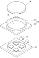
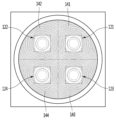
図1は実施例に係るフラッシュモジュール100の投影斜視図であり、図2は実施例に係るフラッシュモジュール100の分解斜視図である。
(Example)
FIG. 1 is a projected perspective view of the
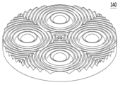
図3は図1に図示された実施例に係るフラッシュモジュール100のI‐I’線を基準とした断面図であり、図4は実施例に係るフラッシュモジュールでレンズ部140の斜視図である。図4において、レンズ部140は図2や図3に図示されたレンズ部140を180°回転して底面が上部に位置するように示された斜視図である。
FIG. 3 is a cross-sectional view of the
図2を参照すると、実施例に係るフラッシュモジュール100はね基板110、複数の発光チップ120と、フレームフレーム130と、レンズ部140のうち少なくとも1つ以上を含むことができる。
Referring to FIG. 2 , the
前記複数の発光チップ120は、複数の発光チップ、例えば相互離隔した2つ以上の発光チップを含むことができる。例えば、実施例において、複数の発光チップ120は、相互離隔した第1発光チップ121、第2発光チップ122、第3発光チップ123及び第4発光チップ124を例示しているが、実施例がこれに限定されるものではない。
The plurality of
実施例において、前記複数の発光チップ120は、半導体化合物、例えばIII族‐V族、II族‐VI族等の化合物半導体で具現することができ、第1導電型半導体層、活性層及び第2導電型半導体層を含むことができるが、これに限定されるものではない。例えば、第1、第2導電型半導体層は、InxAlyGa1-x-yN(0≦x≦1、0≦y≦1、0≦x+y≦1)の組成式を有する半導体物質を含むことができ、例えば、第1、第2導電型半導体層は、GaN、InN、AlN、InGaN、AlGaN、InAlGaN、AlInN、AlGaAs、InGaAs、AlInGaAs、GaP、AlGaP、InGaP、AlInGaP、InPのいずれか1つ以上から形成される。前記第1導電型半導体層はn型半導体層からなることができ、前記第2導電型半導体層はp型半導体層からなることが、これに限定されるものではない。
In an embodiment, the plurality of
前記活性層は、単一量子井戸構造、多重量子井戸構造(MQW:Multi Quantum Well)、量子線(Quantum-Wire)構造または量子ドット(Quantum Dot)構造のうち少なくともいずれか1つから形成される。例えば、前記活性層は、量子井戸/量子壁構造を含むことができる。例えば、前記活性層は、InGaN/GaN、InGaN/InGaN、GaN/AlGaN、InAlGaN/GaN、GaAs/AlGaAs、InGaP/AlGaP、GaP/AlGaPのいずれか1つ以上のペア構造で形成されるが、これに限定されるものではない。 The active layer has at least one of a single quantum well structure, a multiple quantum well structure (MQW), a quantum-wire structure, and a quantum dot structure. . For example, the active layer can include a quantum well/quantum wall structure. For example, the active layer is formed in a pair structure of one or more of InGaN/GaN, InGaN/InGaN, GaN/AlGaN, InAlGaN/GaN, GaAs/AlGaAs, InGaP/AlGaP, and GaP/AlGaP. is not limited to
前記フレームフレーム130は、支持部132とガイド部134を含むことができ、これに対しては図3を参照して詳述することにする。
The
図3を参照すると、実施例に係るフラッシュモジュール100は、所定のキャビティCを含む基板110と、前記基板110のキャビティC内に相互離隔して配置された複数の発光チップ120と、所定の貫通ホールH1(図2参照)を含むガイド部134と、支持部132を含み、前記基板110の上に配置されるフレーム130及び前記ガイド部134の貫通ホールH1内に配置されるレンズ部140を含むことができる。前記基板110は、絶縁材質、例えばセラミック素材を含むことができる。前記セラミック素材は、低温焼成セラミック(LTCC:low temperature co-fired ceramic)または高温焼成セラミック(HTCC:high temperature co-fired ceramic)を含むことができる。また、前記基板110の材質は、AlNからなることができ、熱伝導度が140W/mK以上の金属窒化物で形成することができる。
Referring to FIG. 3, the
また、前記基板110は、別の例として、樹脂系の絶縁物質、例えばPPA(Polyphthalamide)のような樹脂材質またはセラミック材質からなることができる。前記基板110は、シリコンまたはエポキシ樹脂またはプラスチック材質を含む熱硬化性樹脂または高耐熱性、高耐光性材質からなることができる。前記シリコンは、白色系の樹脂を含むことができる。
Alternatively, the
前記基板110内にはキャビティCが形成され、前記キャビティCは、上部が開放された凹状を有することができる。前記キャビティCは、発光チップ120の上側から見るとき、円形、楕円形、多角形形状を有することができるが、これに限定されるものではない。前記キャビティCの側面は、前記キャビティCの底面または所定のリードフレーム(図示しない)の上面に対して、所定の角度で傾斜または垂直するように形成される。
A cavity C is formed in the
前記基板110には、所定のリードフレーム(図示しない)が単数または複数形成され、所定厚さを有する金属プレートからなることができ、前記金属プレートの表面に他の金属層がメッキされるが、これに限定されるものではない。
A predetermined lead frame (not shown) is formed singly or plurally on the
前記リードフレームは、金属材質、例えばチタン(Ti)、銅(Cu)、ニッケル(Ni)、金(Au)、クロム(Cr)、タンタル(Ta)、白金(Pt)、錫(Sn)、銀(Ag)、リン(P)の少なくとも1つまたはこれらの合金のうち少なくとも1つを含み、単層または複数の層に形成される。前記リードフレームは、合金である場合、銅(Cu)と少なくとも一種類の金属合金として、例えば銅-亜鉛合金、銅-鉄合金、銅-クロム合金、銅-銀-鉄のような合金を含むことができる。 The lead frame is made of metal such as titanium (Ti), copper (Cu), nickel (Ni), gold (Au), chromium (Cr), tantalum (Ta), platinum (Pt), tin (Sn), silver. (Ag), at least one of phosphorus (P), or at least one of alloys thereof, and is formed into a single layer or multiple layers. When the lead frame is an alloy, it contains copper (Cu) and at least one metal alloy, such as a copper-zinc alloy, a copper-iron alloy, a copper-chromium alloy, or a copper-silver-iron alloy. be able to.
前記発光チップ120は、前記リードフレームの上に配置され、前記リードフレームと電気的に連結される。前記発光チップ120は、フリップチップ形態の発光チップからなることができるが、実施例がこれに限定されるものではない。
The
実施例において、前記発光チップ120は複数個が配置される。例えば、前記複数の発光チップ120は、少なくとも2つまたはそれ以上配置されるが、これに限定されるものではない。例えば、前記発光チップ120は、第1発光チップ121、第2発光チップ122、第3発光チップ123及び第4発光チップ124を含むことができるが、これに限定されるものではない。例えば、図3では、複数の発光チップ120の例として、第1発光チップ121と第4発光チップ124が図示されているが、これに限定されるものではない。
In an embodiment, a plurality of
前記複数の発光チップ120は、個別的に駆動され、同じ色、例えば白色を発光することができる。
The plurality of light-emitting
図3を参照すると、実施例において、発光チップ120とレンズ部140は所定の距離L2離隔して配置される。
Referring to FIG. 3, in the embodiment, the
例えば、実施例において、第1発光チップ121または第4発光チップ124とレンズ部140の間の光学ギャップ(optical Gap)L2を精密制御して、広角の画角とスリムなフラッシュモジュールを具現することができる。例えば、実施例において、第1発光チップ121または第4発光チップ124とレンズ部140の間の光学ギャップ(optical Gap)L2を約0.2~0.5mmに精密制御して、広角の画角とスリムなフラッシュモジュールを具現することができる。実施例において、第1発光チップ121または第4発光チップ124とレンズ部140の間の光学ギャップ(optical Gap)L2が0.2mm未満である場合、光学距離が狭くなることで、配光特性が狭くなり過ぎる問題があり、0.5mmを超える場合、光学距離が広くなることで、配光特性が広くなり過ぎる問題がある。
For example, in the embodiment, the optical gap L2 between the first
また、実施例において、基板110とフレーム130を合わせた厚さL1は、発光チップの高さHの約4倍~6倍の範囲の厚さに制御されることで、広角の画角を提供することができ、カメラの撮像領域に均一な光の分布の具現が可能であり、スリムなフラッシュモジュールを具現することができる。
In addition, in the embodiment, the combined thickness L1 of the
例えば、第4発光チップ124aの高さHが約0.3mmである場合、基板110とフレーム130を合わせた厚さL1は、1.2mm~1.8mmの範囲を有することができる。実施例において、基板110とフレーム130を合わせた厚さL1が発光チップの高さHの4倍未満である場合、フラッシュモジュールの厚さが携帯電話等で占める空間が小さく、エアーギャップ(air gap)が大き過ぎて光特性が低下する問題がある。
For example, when the height H of the fourth
一方、実施例において、基板110とフレーム130を合わせた厚さL1が発光チップの高さHの6倍を超える場合、フラッシュモジュールの厚さが携帯電話等で占める体積が大き過ぎて発光された光が適切な分散分布ができず、フラッシュモジュールが装着される携帯電話等の機構との干渉により組立てることができない問題がある。
On the other hand, in the embodiment, if the total thickness L1 of the
また、実施例において、フラッシュモジュールの基板110の外側幅S1は、発光チップ121、124の水平幅Wの約3倍~5倍の範囲の幅を有し、発光チップから発光される光の均一な分布の具現が可能であり、スリムながらもコンパクトなフラッシュモジュールを提供することができる。
In addition, in the embodiment, the outer width S1 of the
例えば、前記フラッシュモジュールに装着される発光チップの水平幅Wが約1.1mmである場合に、前記基板110の外側幅S1は約3.3mm~約5.5mmを有することができる。また、前記基板110の外側幅S1は約4.6mm~5.2mmに制御されることで、広角を提供すると共に光の均一な分布の具現が可能であり、スリムながらもよりコンパクトなフラッシュモジュールを提供することができる。
For example, when the horizontal width W of the light emitting chip mounted on the flash module is about 1.1 mm, the outer width S1 of the
前記基板110の外側幅S1が発光チップ121、124の水平幅Wの3倍未満である場合、発光チップ間の光の干渉等によって光特性が低下する。一方、前記基板110の外側幅S1が発光チップ121、124の水平幅Wの5倍を超える場合、発光チップ間の離隔距離S3の増大により、均一な光の分布を提供できなかったり、コンパクトなフラッシュモジュールを提供し難くなる。
If the outer width S1 of the
また、実施例のフラッシュモジュールにおいて、基板110の内側キャビティCの幅S2は、発光チップ121、124の水平幅Wの約2倍~約4倍の範囲を有することができ、これによって、レンズ部140の配置分布と発光チップの分布制御を適切にすることができ、発光チップから発光された光の均一な分布の具現が可能であり、スリムながらもコンパクトなフラッシュモジュールを提供することができる。
In addition, in the flash module of the embodiment, the width S2 of the inner cavity C of the
例えば、前記フラッシュモジュールに装着される発光チップの水平幅Wが約1.1mmである場合に、前記基板110の内側キャビティCの幅S2は、約2.2mm~4.4mmを有することができる。また、前記基板110の内側キャビティCの幅S2は、約3.5mm~4.0mmに制御されることで、発光チップから発光された光のより均一な分布の具現が可能であり、スリムながらもコンパクトなフラッシュモジュールを提供することができる。
For example, when the horizontal width W of the light emitting chip mounted on the flash module is about 1.1 mm, the width S2 of the inner cavity C of the
前記基板110の内側キャビティCの幅S2が発光チップ121、124の水平幅Wの2倍未満である場合、発光チップ間の光の干渉等によって光特性が低下する。一方、前記基板110の内側キャビティCの幅S2が発光チップ121、124の水平幅Wの4倍を超える場合、レンズ部140が発光チップより肥大になり、発光チップ間の離隔距離S3の増大により、均一な光の分布を提供できなかったり、コンパクトなフラッシュモジュールを提供し難くなる。
If the width S2 of the inner cavity C of the
また、実施例において、前記基板110の内側キャビティCに配置される発光チップ121、124の間の距離S3は、発光チップ121、124自体の水平幅Wの約1/2倍~1.0倍の範囲に制御されることで、広角の画角を提供すると共にカメラの撮像領域に均一な光の分布の具現が可能となる。
Also, in an embodiment, the distance S3 between the
一方、前記基板110の内側キャビティCに配置される発光チップ121、124の間の距離S3が発光チップ121、124自体の水平幅Wの1/2倍未満である場合、発光チップ装着時工程上のイシューが発生する可能性があり、装着後発光チップから発生する熱によって、光特性、電気的特性が低下する問題が発生する。
On the other hand, if the distance S3 between the
一方、前記基板110の内側キャビティCに配置される発光チップ121、124の間の距離S3が発光チップ121、124自体の水平幅Wの1倍を超える場合、レンズ部140の光拡散パターンP1、P2と上下間のアラインが困難となり、均一な光分布の具現が難しくなる。
On the other hand, when the distance S3 between the
また、実施例において、¥発光チップ121、124と基板110の側面の間の距離S4は、発光チップ121、124自体の水平幅Wの約1/2倍~1.0倍の範囲に制御されることで、カメラの撮像領域に均一な光の分布の具現が可能であり、広角の画角を提供することができ、コンパクトなフラッシュモジュールを提供することができる。
In the embodiment, the distance S4 between the
一方、発光チップ121、124と基板110の側面の間の距離S4が発光チップ121、124自体の水平幅Wの1倍を超える場合、レンズ部140の光拡散パターンP1、P2と上下間にミスアラインが発生する可能性が増加し、均一な光分布の具現が難しくなる。
On the other hand, when the distance S4 between the
一方、発光チップ121、124と基板110の側面の間の距離S4が発光チップ121、124自体の水平幅Wの1/2倍未満である場合、発光チップ装着時工程上のイシューが発生する可能性があり、装着後発光チップから発生する熱によって、光特性、電気的特性が低下する問題が発生する。
On the other hand, if the distance S4 between the
実施例に係るフラッシュモジュール100に装着されるレンズ部140は、複数の光拡散パターンP1、P2を含むことで、発光チップ120から発光された光の光拡散を高めて広角の画角(FOV)を具現することができる。例えば、発光モジュールに第1発光チップ121と第4発光チップ124に対応して第2光拡散パターンP2、第1光拡散パターンP1を含むことができ、実施例のように発光チップが4個である場合、光拡散パターンは4個備えられる。
The
図3を再参照すると、前記複数の発光チップ120の上には蛍光体層121b、124bが配置される。例えば、前記第1発光チップ121は、青色LEDチップ121aと第1黄色蛍光体層121bを含むことができる。また、前記第4発光チップ124は、青色LEDチップ124aと第4黄色蛍光体層124bを含むことができる。
Referring back to FIG. 3, phosphor layers 121b and 124b are disposed on the plurality of
また、前記第2発光チップ122は、第2LEDチップ(図示しない)と第2蛍光体層(図示しない)を含むことができ、前記第3発光チップ123は、第3LEDチップ(図示しない)と第3蛍光体層(図示しない)を含むことができる。
Also, the second
また、発光チップ120が青色LEDチップである場合に、前記蛍光体層は、緑色蛍光体、赤色蛍光体または青色蛍光体の少なくとも1つ以上を含むことができる。
Also, when the
実施例は、例えば青色蛍光体:緑色蛍光体:赤色蛍光体の含有量比率(wt%)を40~60%:10~20%:25~45t%に制御することで、鮮明なカメラフラッシュを具現することができる。 In the embodiment, for example, by controlling the content ratio (wt%) of blue phosphor: green phosphor: red phosphor to 40 to 60%: 10 to 20%: 25 to 45t%, a clear camera flash can be obtained. can be embodied.
例えば、前記青色蛍光体のピーク(Peak)波長は約450nmであり、前記緑色蛍光体のピーク(Peak)波長は約517nmであり、前記赤色蛍光体のピーク(Peak)波長は約661nmであるが、これに限定されるものではない。 For example, the blue phosphor has a peak wavelength of about 450 nm, the green phosphor has a peak wavelength of about 517 nm, and the red phosphor has a peak wavelength of about 661 nm. , but not limited to.
実施例において、前記緑色蛍光体の半値幅は50~60であり、前記赤色蛍光体の半値幅は90~100であるが、これに限定されるものではない。 In an embodiment, the FWHM of the green phosphor is 50-60, and the FWHM of the red phosphor is 90-100, but is not limited thereto.
図4及び図5を参照して、本実施例の技術的課題を解決するための技術的解決手段及び技術的効果をもう少し詳述することにする。 With reference to FIGS. 4 and 5, the technical solutions and technical effects for solving the technical problems of this embodiment will be described in more detail.
実施例の課題の1つは、鮮明な色の具現が可能なフラッシュモジュール、及び端末機を提供することである。 One object of the embodiments is to provide a flash module and a terminal capable of realizing vivid colors.
図4は太陽光の波長スペクトルS、比較例の発光波長スペクトルPS及び実施例に係るフラッシュモジュールの発光チップから発光スペクトルESの比較例示図であり、図5は実施例と比較例のCIE色座標及び色再現範囲の例示図である。 FIG. 4 is a comparative illustration of the wavelength spectrum S of sunlight, the emission wavelength spectrum PS of the comparative example, and the emission spectrum ES from the light emitting chip of the flash module according to the example, and FIG. 5 is the CIE color coordinates of the example and the comparative example. and an exemplary diagram of a color reproduction range.
従来技術のフラッシュモジュールにおいて、発光チップは青色LEDチップの上に緑色蛍光体と赤色蛍光体を含めて白色光を具現している。 In the prior art flash module, the light-emitting chip includes a green phosphor and a red phosphor on a blue LED chip to realize white light.
例えば、従来技術の発光チップは、420nm~450nmの発光波長の青色LEDチップの上に、発光波長が約530nmである緑色蛍光体と発光波長が約630nmの赤色蛍光体を含めて白色光を具現している。 For example, a conventional light emitting chip implements white light by including a green phosphor with an emission wavelength of about 530 nm and a red phosphor with an emission wavelength of about 630 nm on a blue LED chip with an emission wavelength of 420 nm to 450 nm. are doing.
これによって、図4のように、従来技術(比較例)の発光波長スペクトルPSは、太陽光の波長スペクトルSに対応するように、全体的に均一な波長分布を示すことができなかった。 As a result, as shown in FIG. 4, the emission wavelength spectrum PS of the prior art (comparative example) could not exhibit a wholly uniform wavelength distribution so as to correspond to the wavelength spectrum S of sunlight.
即ち、カメラで鮮明な色(vivid color)を具現するためにカメラフラッシュ(Flash)の役割が重要であるが、鮮明な色(vivid color)はCQS(Color Quality Scale)指数によって表現されるが、従来技術では太陽光の波長スペクトルSに対応する均一な波長分布を具現できないので、CQS(Color Quality Scale)指数が約70~80程度に留まっており、鮮明な色の具現に限界がある。 That is, the camera flash plays an important role in realizing vivid colors in the camera, and the vivid colors are represented by the CQS (Color Quality Scale) index. Since the conventional technology cannot realize a uniform wavelength distribution corresponding to the wavelength spectrum S of sunlight, the CQS (Color Quality Scale) index remains at about 70 to 80, which limits the realization of clear colors.
例えば、従来技術のフラッシュモジュールに採用される発光チップは、約410nm以下の領域では発光波長の強度(intensity)が弱く、緑色蛍光体領域のうちに約500nmの領域と赤色蛍光体領域のうちに約650nm以上の領域で発光波長スペクトルが微弱な問題があるので、CQS(Color Quality Scale)指数が低く、鮮明な色(vivid color)の具現に限界があった。 For example, the light-emitting chip employed in the conventional flash module has a weak emission wavelength intensity in the region below about 410 nm, and has a low intensity in the region of about 500 nm in the green phosphor region and in the red phosphor region. Since there is a problem that the emission wavelength spectrum is weak in the region of about 650 nm or more, the CQS (Color Quality Scale) index is low, and vivid colors are limited.
一方、UV波長(365~385nm)を適用したときには、人体に有害な問題があるので、携帯電話用のフラッシュの発光チップとして採用できない問題がある。 On the other hand, when a UV wavelength (365 to 385 nm) is applied, there is a problem that it is harmful to the human body, so there is a problem that it cannot be used as a flash light emitting chip for mobile phones.
実施例は、鮮明な色(vivid color)を具現するために、発光チップ120が青色LEDチップである場合に、前記蛍光体層は、緑色蛍光体、赤色蛍光体または青色蛍光体の少なくとも1つ以上を含むことができる。例えば、実施例の蛍光体組成物は、緑色蛍光体、赤色蛍光体を含むことができるが、これに限定されるものではない。
In one embodiment, when the light-emitting
また、実施例は、図4のように、発光チップ120が青色LEDチップである場合に、前記蛍光体層は、緑色蛍光体、赤色蛍光体及び青色蛍光体を含むことができる。
In addition, as shown in FIG. 4, when the
例えば、実施例の蛍光体組成物において、青色蛍光体:緑色蛍光体:赤色蛍光体の含有量比率(wt%)を40~60%:10~20%:25~45%に制御することで、より鮮明なカメラフラッシュを具現することができる。一方、前記実施例の蛍光体組成物の含有量比率を外れる場合、所望のスペクトル(Spectrum)を具現することが困難であり、光効率が落ちる問題がある。 For example, in the phosphor composition of the example, by controlling the content ratio (wt%) of blue phosphor: green phosphor: red phosphor to 40 to 60%: 10 to 20%: 25 to 45% , a clearer camera flash can be realized. On the other hand, when the content ratio of the phosphor composition is out of the above range, it is difficult to realize a desired spectrum, and light efficiency is lowered.
具体的に、図4のように、実施例の蛍光体組成物は、発光チップの発光中心波長が400nm~420nmである場合、前記発光チップの400nm~420nmの発光中心波長の波長強度(EB1領域)は、太陽光源の400nm~420nmの波長強度より大きい。 Specifically, as shown in FIG. 4, when the emission center wavelength of the light-emitting chip is 400 nm to 420 nm, the phosphor composition of the example has a wavelength intensity (EB1 region ) is greater than the 400-420 nm wavelength intensity of the solar light source.
また、実施例において、赤色蛍光体は、前記発光チップの400nm~420nmの発光波長を励起波長とした発光中心波長が650nm~670nmであり、前記赤色蛍光体の650nm~670nmの励起中心波長の波長強度(ER領域)が太陽光源の650nm~670nmの波長強度より大きい。 In the embodiment, the red phosphor has an emission center wavelength of 650 nm to 670 nm when the emission wavelength of the light emitting chip of 400 nm to 420 nm is used as an excitation wavelength, and the excitation center wavelength of the red phosphor is 650 nm to 670 nm. The intensity (ER region) is greater than the 650 nm to 670 nm wavelength intensity of the solar light source.
例えば、実施例に係るフラッシュモジュールの波長スペクトルム(ES)の650nm~670nmにおける波長強度(ER)が太陽光源波長スペクトルSの650nm~670nmの波長強度の約10%~30%の範囲まで大きく確保されることで、鮮明な色(Vivid color)の具現が可能である。 For example, the wavelength intensity (ER) at 650 nm to 670 nm of the wavelength spectrum (ES) of the flash module according to the embodiment is ensured to be large in the range of about 10% to 30% of the wavelength intensity of 650 nm to 670 nm of the sunlight light source wavelength spectrum S. By doing so, it is possible to implement vivid colors.
反面、従来技術の発光チップは、400nm~420nmにおける波長強度が微弱であり、赤色蛍光体の650nm~670nmにおける波長強度も微弱である。 On the other hand, the conventional light-emitting chip has a weak wavelength intensity in the range of 400 nm to 420 nm, and the wavelength intensity of the red phosphor in the range of 650 nm to 670 nm is also weak.
よって、従来技術では、CQS(Color Quality Scale)指数が約80.0であり、CRIも77.0であったが、実施例では、CQS(Color Quality Scale)指数が約92.1として非常に上昇しており、CRIも90.2として著しく上昇した。 Therefore, in the prior art, the CQS (Color Quality Scale) index was about 80.0 and the CRI was also 77.0. and the CRI also rose significantly as 90.2.
また、CRIでは純粋な赤色であるR9データを重要に取り扱うが、従来技術では約‐11.1であったが、実施例では70.6として著しく上昇した。 Also, the CRI values pure red R9 data, which was about -11.1 in the prior art, but increased significantly to 70.6 in the example.
よって、実施例によれば、CQS(Color Quality Scale)指数及びCRI指数が著しく上昇し、非常に鮮明な色(Vivid color)を具現することができる。 Therefore, according to the embodiment, CQS (Color Quality Scale) index and CRI index are remarkably increased, and very vivid colors can be realized.
また、実施例において、赤色蛍光体の半値幅(FWHM)は約90~100となることで、従来技術における赤色蛍光体の半値幅が約70nmであること比べて、実施例は赤色波長の分布範囲を広くすることで、鮮明な色に寄与することができる。 In addition, in the embodiment, the red phosphor has a half-value width (FWHM) of about 90 to 100. Compared to the red phosphor in the prior art, which has a half-value width of about 70 nm, the red wavelength distribution of the example is A wider range can contribute to vivid colors.
また、実施例の蛍光体組成物は、緑色蛍光体を含むことができ、前記緑色蛍光体は、前記発光チップ120の400nm~420nmの発光波長を励起波長とした発光中心波長が505nm~525nmである。
In addition, the phosphor composition of the embodiment can contain a green phosphor, and the green phosphor has an emission central wavelength of 505 nm to 525 nm when the emission wavelength of the
これによって、505nm~525nmの範囲では、波長スペクトルの波長強度を従来技術より改善することで、鮮明な色の具現が可能である。 Accordingly, in the range of 505 nm to 525 nm, by improving the wavelength intensity of the wavelength spectrum compared to the prior art, vivid colors can be realized.
例えば、従来技術の波長スペクトルPSでは、505nm~525nmにおける波長強度が太陽光源波長スペクトルSの波長強度の約50%未満、例えば30%であったが、実施例に係るフラッシュモジュールにおける波長スペクトルESの505nm~525nmにおける波長強度が太陽光源波長スペクトルSの波長強度の約60%以上、例えば約70%まで移動可能であり、色純度を著しく向上させることで、鮮明な色(Vivid color)の具現が可能となる。 For example, in the prior art wavelength spectrum PS, the wavelength intensity at 505 nm to 525 nm was less than about 50%, such as 30%, of the wavelength intensity in the solar light source wavelength spectrum S, whereas the wavelength spectrum ES in the example flash module The wavelength intensity at 505 nm to 525 nm can be shifted to about 60% or more, for example, about 70% of the wavelength intensity of the solar light source wavelength spectrum S, and the color purity is significantly improved, so that vivid colors can be realized. It becomes possible.
また、前記緑色蛍光体の半値幅は50~60であり、従来技術における緑色蛍光体の半値幅が約30nmであることに比べて、実施例の緑色波長の分布範囲を広くすることで、鮮明な色に寄与することができる。 In addition, the half width of the green phosphor is 50 to 60, and compared with the half width of about 30 nm of the green phosphor in the prior art, by widening the distribution range of the green wavelength in the example, the clear can contribute to the color.
また、実施例において、蛍光体組成物は青色蛍光体を含むことができ、前記青色蛍光体は、前記発光チップ120の400nm~420nmの発光波長を励起波長とした発光中心波長(EB2領域)が455nm~465nmである。
Further, in an embodiment, the phosphor composition may contain a blue phosphor, and the blue phosphor has an emission central wavelength (EB2 region) excited by an emission wavelength of 400 nm to 420 nm of the
これによって、455nm~465nmの波長領域で、波長スペクトルの波長強度を従来技術に比べて向上させることで、太陽光の波長スペクトルに近接した波長スペクトルを具現することで、より鮮明な色の具現が可能である。 Accordingly, in the wavelength region of 455 nm to 465 nm, the wavelength intensity of the wavelength spectrum is improved compared to the conventional technology, and a wavelength spectrum close to the wavelength spectrum of sunlight is realized, thereby realizing clearer colors. It is possible.
図5は、実施例と比較例のCIE色座標及び色再現範囲(N)の例示図である。 FIG. 5 is an illustration diagram of the CIE color coordinates and the color gamut (N) of the example and the comparative example.
実施例によって鮮明な色(vivid color)を具現するためには、高い色再現率が必要とされるが、従来技術は色再現率が低く、鮮明な色(vivid color)の具現に限界があった。 Although a high color reproduction rate is required to implement vivid colors according to the embodiments, the conventional technology has a low color reproduction rate and is limited in realizing vivid colors. rice field.
図5を説明すると、CIE色座標におけるNTSC色再現範囲(N)、実施例の色再現範囲(EC)と従来技術の色再現範囲(PC)の例示図である。 FIG. 5 is an illustration of the NTSC color gamut (N) in the CIE color coordinates, the color gamut (EC) of the embodiment, and the color gamut (PC) of the prior art.
一方、先述したように、既存のLEDで色再現率を向上するための解決方案として、緑色蛍光体の発光波長や赤色蛍光体の発光波長をより深い(deep)側に移動しなければならないが、従来の赤色蛍光体は、発光波長が長波長として移動できない短所がある。 On the other hand, as mentioned above, in order to improve the color reproducibility of existing LEDs, the emission wavelength of the green phosphor and the emission wavelength of the red phosphor should be shifted to a deeper side. However, conventional red phosphors have a shortcoming in that they have a long emission wavelength and cannot move.
このような課題を解決するための実施例に係る蛍光体組成物は、Mg2Ge2O3F2:Mn4+または(Sr、Mg)GeOF:Mn4+系の赤色蛍光体を含めて青色発光波長を励起波長として白色光源の3波長スペクトルを具現することができる。このような蛍光体組成物は、赤色蛍光体組成物に対する具体的な具現例であり、このような組成の他に青色発光波長を励起波長として赤色波長スペクトルを発光できる赤色蛍光体も可能である。 A phosphor composition according to an embodiment for solving such a problem includes a Mg 2 Ge 2 O 3 F 2 :Mn 4 + or (Sr, Mg)GeOF:Mn 4 + -based red phosphor. A three-wavelength spectrum of a white light source can be realized using a blue emission wavelength as an excitation wavelength. Such a phosphor composition is a specific example of a red phosphor composition, and in addition to such a composition, a red phosphor capable of emitting light in a red wavelength spectrum using a blue emission wavelength as an excitation wavelength is also possible. .
実施例によれば、新規で差別化されたMg2Ge2O3F2:Mn4+または(Sr、Mg)GeOF:Mn4+系の赤色蛍光体を開発することで、最大強度を有する発光ピーク(peak)を従来技術(R1)に比べて約650nm~670nmまで(R2)向上させることで、実施例の色再現率を著しく向上させることができる。例えば、実施例の(Sr、Mg)GeOF:Mn4+系の赤色蛍光体は(Sr、Mg)4GeO3F2:Mn4+であるが、これに限定されるものではない。 According to the embodiment, by developing new and differentiated Mg2Ge2O3F2 : Mn4 + or (Sr,Mg)GeOF: Mn4 + based red phosphors, having maximum intensity By increasing the emission peak (peak) to about 650 nm to 670 nm (R2) compared to the prior art (R1), the color reproduction rate of the embodiment can be significantly improved. For example, the (Sr,Mg)GeOF: Mn4 +-based red phosphor of the embodiment is (Sr,Mg) 4GeO3F2 : Mn4 +, but is not limited thereto.
また、実施例の蛍光体組成物において、緑色蛍光体はBaMgAl10O17:Eu2+、Mn4+であるが、これに限定されるものではない。このような蛍光体組成物は、緑色蛍光体組成物に対する具体的な具現例であり、このような組成の他に青色発光波長を励起波長として緑色波長スペクトルを発光できる赤色蛍光体も可能である。 In addition, in the phosphor compositions of the examples, the green phosphor is BaMgAl 10 O 17 :Eu 2 +, Mn 4 +, but is not limited to this. Such a phosphor composition is a specific example of a green phosphor composition, and in addition to such a composition, a red phosphor capable of emitting green wavelength spectrum with a blue emission wavelength as an excitation wavelength is also possible. .
実施例によれば、新規で差別化されたBaMgAl10O17:Eu2+、Mn4+の緑色蛍光体の開発することで、最大強度を有する発光ピーク(peak)を従来技術(G1)に比べて約505nm~525nmまで(G2)向上させることで、実施例の色再現率を著しく向上させることができる。 According to the embodiment, by developing a novel and differentiated BaMgAl 10 O 17 :Eu 2 +, Mn 4 + green phosphor, the emission peak with the maximum intensity can be obtained compared to the conventional technology (G1). By improving (G2) from about 505 nm to 525 nm, the color reproducibility of the embodiment can be remarkably improved.
実施例によって高い色再現率の具現が可能となることで、鮮明な色(vivid color)を具現できる蛍光体組成物、フラッシュモジュール及び端末機を提供することができる。 By implementing a high color reproduction rate according to the embodiment, it is possible to provide a phosphor composition, a flash module, and a terminal capable of implementing vivid colors.
また、実施例の技術的課題の1つは、端末機のカメラの技術的発展傾向に対応できるように、カメラフラッシュ(Flash)も広角の画角(FOV)の具現が可能なフラッシュモジュール及びこれを含む端末機を提供することである。 In addition, one of the technical problems of the embodiments is a flash module capable of realizing a wide field of view (FOV) for the camera flash (Flash) so as to correspond to the technological development trend of the camera of the terminal. It is to provide a terminal including
また、実施例の技術的課題の1つは、端末機のスリム化(slim)トレンドと広角の画角(FOV)の技術的特性を同時に満足できるフラッシュモジュール及びこれを含む端末機を提供することである。 In addition, one of the technical problems of the embodiments is to provide a flash module and a terminal including the flash module that satisfy both the slim trend of the terminal and the technical characteristics of a wide field of view (FOV) at the same time. is.
前記技術的課題を解決するために、図3のように実施例は、所定の貫通ホールH1を有するガイド部134と、支持部132を含み、前記基板110の上に配置されるフレームフレーム130及び前記ガイド部134の貫通ホールH1内に配置されるレンズ部140を含むことができる。
In order to solve the technical problem, as shown in FIG. 3, the embodiment includes a
実施例において、前記フレーム130は、樹脂系の絶縁物質、例えばPPA(Polyphthalamide)のような樹脂材質またはセラミック材質からなることができる。また、前記フレーム130は、シリコンまたはエポキシ樹脂またはプラスチック材質を含む熱硬化性樹脂または高耐熱性、高耐光性材質からなることができる。前記シリコンは、白色系の樹脂を含むことができる。また、前記フレーム130は、W-EMCまたはW-Silicone等で形成される。
In some embodiments, the
実施例において、前記レンズ部140は、プラスチック材質、例えばアクリル系プラスチック材料を用いることができ、例えばPMMA(Polymethyl methacrylate)をあげることができるが、これに限定されるものではない。実施例で採用されるレンズ部140の材質であるPMMAは、ガラスより透明性が優れ、加工及び成形が容易である長所がある。
In an embodiment, the
実施例において、前記レンズ部140は、光抽出レンズまたは光拡散レンズのようなレンズとして機能することができ、前記発光チップ120から放出された光の指向特性を変化させるための部材であり、特に限定されるものではないが、屈折率が1.4以上1.7以下である透明材料を利用することができる。
In an embodiment, the
また、レンズ部140は、ポリカーボネート(PC)またはエポキシ樹脂(EP)の透明樹脂材料や透明なガラス(Glass)、EMCまたはSiliconeによって形成されるが、これに限定されるものではない。
In addition, the
以下、図2と図3を参照して、実施例においてフレーム130内にレンズ部140が支持される原理とそのようになる場合に有利な技術的効果を記述する。
Hereinafter, with reference to FIGS. 2 and 3, the principle of supporting the
実施例では、フレーム130のガイド部134とレンズ部140の二重射出構造を有することができるので、接着工程が非常に効率的になり、特にカメラフラッシュモジュールの厚さを非常にスリム化することができる。
In an embodiment, it can have a double injection structure of the
従来技術では、レンズ部を含んだフラッシュモジュールの厚さは約2.5mm以上であり、その以下に厚さを減らすことができない問題があった。これは、従来技術では発光モジュールをパッケージ基板にSMT(Surface Mounting Technology)作業した後、レンズを別途にカメラカバーケース(Cover Case)に付けるので、カメラフラッシュモジュールの厚さをスリム化することに限界があった。 In the prior art, the thickness of the flash module including the lens portion is about 2.5 mm or more, and there is a problem that the thickness cannot be reduced below that. This is because the conventional technology attaches the lens to the camera cover case after applying SMT (Surface Mounting Technology) to the light emitting module on the package substrate, which limits the thickness of the camera flash module. was there.
反面、実施例によって、レンズ部140がフレーム130のガイド部134内に射出構造で形成されることで、カメラフラッシュモジュール100自体の厚さを約1.4mmまで非常にスリムに形成できる有利な技術的効果がある。実施例で、レンズ部140の厚さはカメラフラッシュモジュール100の全体厚さの約1/2以下に制御することができ、カメラフラッシュモジュール100自体の厚さを非常にスリムに形成することができる。
On the other hand, according to the embodiment, the
また、従来技術によれば、レンズを別途にカメラカバーケース(Cover Case)に付けるか、ピンコンタクト(Pin Contact)等の方式を用いるので、厚さが増加すると共に、付着等で問題が発生した。 In addition, according to the prior art, the lens is separately attached to the camera cover case or a pin contact method is used, which increases the thickness and causes problems such as adhesion. .
反面、実施例では、カメラケース(図示しない)にカメラフラッシュモジュール100に対応する大きさの孔が備えられSMT Typeで装着されるので、携帯電話ケースと別途に結合しなくてもよいので、携帯電話の全体組立工程が非常に容易であり、堅固な結合を得ることができ、スリムな携帯用端末機を具現できる有利な技術的効果がある。
On the other hand, in the embodiment, a camera case (not shown) is provided with a hole having a size corresponding to the
また、実施例によれば、前記レンズ部140の上面は、前記フレーム130のガイド部134と同一または低い位置に配置されるようにすることで、スリムなカメラモジュールの具現すると共に、広角の画角(FOV)を得ることができる有利な技術的効果がある。
In addition, according to the embodiment, the top surface of the
例えば、実施例のカメラモジュールは、フレームのガイド134外に別途にレンズ部140を結合するためのカメラケースや他の結合部がないので、カメラフラッシュから発光される光を遮断する領域を最小化できるので、フレームの厚さ、傾き等の設計等によって、最大限広角を具現できる有利な技術的効果がある。
For example, since the camera module of the embodiment does not have a camera case or other coupling parts for separately coupling the
また、実施例で、発光チップ120とレンズ部140の間の光学ギャップ(optical Gap)Lを精密制御して、広角の画角と共にスリムなフラッシュモジュールを具現できる有利な技術的効果がある。例えば、実施例で、発光チップ120とレンズ部140の間の光学ギャップ(optical Gap)Lを約0.3~0.5mmに精密制御して、広角の画角と共にスリムなフラッシュモジュールを具現できる技術的効果がある。
In addition, in the embodiment, the optical gap L between the light emitting
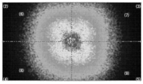
図6は実施例に係るフラッシュモジュールにおけるレンズ部の斜視図であり、図7は実施例に係るフラッシュモジュールの光分布データであり、図8は実施例に係るフラッシュモジュールにおけるレンズ部と発光チップの投影図である。 FIG. 6 is a perspective view of the lens portion in the flash module according to the example, FIG. 7 is light distribution data of the flash module according to the example, and FIG. It is a projection view.
実施例の技術的課題の1つは、広角の画角(FOV)を具現すると共に、カメラの撮像領域に均一な光分布の具現が可能なフラッシュモジュール及びこれを含む端末機を提供することである。 One of the technical problems of the embodiments is to provide a flash module and a terminal including the same capable of realizing a wide field of view (FOV) and realizing uniform light distribution in an imaging area of a camera. be.
また、実施例の技術的課題の1つは、発光モジュールの発光チップとフラッシュレンズのアライン精度を著しく向上させて、組立工程の効率性、堅固性を高めながらも、均一な光分布を具現できるフラッシュモジュール及びこれを含む端末機を提供することである。 In addition, one of the technical problems of the embodiment is that the alignment accuracy of the light-emitting chip and the flash lens of the light-emitting module can be remarkably improved, and the efficiency and robustness of the assembly process can be improved, and uniform light distribution can be achieved. To provide a flash module and a terminal including the same.
図6と図8を参照すると、実施例に係るレンズ部140は複数の光拡散パターンを含むことができる。例えば、発光チップ120が4個である場合、これに対応して第1光拡散パターン141、第2光拡散パターン142、第3光拡散パターン143及び第4光拡散パターン144を含むことができるが、これに限定されるものではない。
Referring to FIGS. 6 and 8, the
実施例で、複数の発光チップ120から放出される光(Ray)の分布とレンズ部140の光拡散パターンの一致度が高いほど、広角の画角(FOV)と共に均一な光分布が得られる技術的効果がある。
In the embodiment, the higher the degree of matching between the light (ray) distribution emitted from the plurality of
また、実施例で、発光チップ120がレンズ部140の上面図(top view)において、各光拡散パターン141、142、143、144に発光チップ121、122、123、124が配置され、各光拡散パターンの中心と各発光チップのセンターが一致する技術的効果がある。
In the embodiment, the light-emitting
従来技術では、発光モジュールを基板に別途にSMT作業し、レンズを別途に携帯電話のカバーケース(Cover Case)に付けるので、従来技術はSMT公差とレンズ付着公差等に約50μm以上の公差の発生が不可避であり、これは均一な光分布を得られなくなる結果を招いた。 In the conventional technology, the light emitting module is separately SMT-worked on the substrate, and the lens is separately attached to the cover case of the mobile phone, so the conventional technology has a tolerance of 50 μm or more in SMT tolerance and lens attachment tolerance. was unavoidable, which resulted in an inability to obtain a uniform light distribution.
これに対し、実施例は、二重射出により一体形成されたレンズ部とフレームを基板と一回接着するだけでよいので、接着が容易であるだけではなく、厚さをスリム化することができ、さらに発光チップとレンズ部の光拡散パターンとのアラインを非常に精密に制御できる有利な技術的効果がある。 On the other hand, in the embodiment, the lens part and the frame, which are integrally formed by double injection, need only be adhered to the substrate only once. Furthermore, there is the advantageous technical effect that the alignment between the light emitting chip and the light diffusion pattern of the lens can be controlled very precisely.
例えば、実施例はレンズ部の光拡散パターンと発光チップのアライン公差を約25μm以下に制御することで、発光チップから発光される光の指向角特性とレンズ部の光拡散パターンの一致性を著しく向上させ、広角の画角(FOV)の具現と共に配光特性を向上させて均一な光分布を得ることができる有利な技術的効果がある。 For example, in the embodiment, by controlling the alignment tolerance between the light diffusion pattern of the lens portion and the light emitting chip to about 25 μm or less, the matching between the directivity angle characteristics of the light emitted from the light emitting chip and the light diffusion pattern of the lens portion is significantly improved. It is possible to obtain a uniform light distribution by improving light distribution characteristics as well as realizing a wide field of view (FOV).
また、実施例によれば、レンズ部140のセンターと各発光チップ120のセンターの間の距離が約70μm以下に制御されることで、広角を具現しながらも均一な光分布を得ることができる有利な技術的効果がある。
In addition, according to the embodiment, the distance between the center of the
従来技術では、フレームとPCB、フレームとレンズの2回の接着が行われていたが、実施例では、二重射出により一体形成されたレンズ部とフレームを基板と一回接着するだけでよいので、接着が容易であるだけではなく、厚さをスリム化することができ、さらに発光チップとレンズ部の光拡散パターンとのアラインを非常に精密に制御して、広角の画角(FOV)の具現と共に非常に均一な光分布を得ることができる有利な技術的効果がある。 In the prior art, the frame and the PCB and the frame and the lens were adhered twice, but in the embodiment, the lens part and the frame, which are integrally formed by double injection, need only be adhered once to the substrate. , Not only is it easy to attach, it can be slimmed down, and the alignment between the light-emitting chip and the light diffusion pattern on the lens can be controlled very precisely to achieve a wide field of view (FOV). There is an advantageous technical effect that a very uniform light distribution can be obtained with the implementation.
図7を参照すると、実施例は、以下の表1の均一な光特性分布を得ることができる。

現在、広角カメラ技術によって、業界で要求されるフラッシュモジュールの画角(FOV)は、デュアルカメラ(Dual Camera)が持続開発されることで、約120°以上の広角を要求する状況であり、さらに広角における均一な光分布特性も同時に具現しなければならないが、広角を具現する場合には、均一な光分布の具現が難しくなる技術的矛盾に逢着している状態である。 Currently, due to the wide-angle camera technology, the field of view (FOV) of the flash module required by the industry requires a wide angle of about 120 degrees or more due to the continuous development of dual cameras. A uniform light distribution characteristic at a wide angle should also be realized at the same time.
一方、実施例によれば、カメラフラッシュの画角(FOV)は、120°まで具現可能であり、135°までも具現が可能である。 Meanwhile, according to the embodiment, the angle of view (FOV) of the camera flash can be implemented up to 120 degrees, and can be implemented up to 135 degrees.
図7及び表1は、画角(FOV)が135°である場合の光分布データである。1.0Fと0.7Fは、F(field)がそれぞれ1.0、0.7である時、1M距離で角度にとよる照度(lx)値であり、1.0Fでは平均8.48lxであり、0.7Fでは平均28.9lxであり、これは業界で要求する以上の照度基準の効果が表れたものであり、発明者の既存の発明(未公開)に比べても、中心照度よりF(フィールド)別の配光特性がそれぞれ4.5%と15.3%も著しく向上した技術的効果である。 FIG. 7 and Table 1 are light distribution data when the angle of view (FOV) is 135°. 1.0F and 0.7F are the illuminance (lx) values depending on the angle at 1M distance when F(field) is 1.0 and 0.7 respectively, and average 8.48lx at 1.0F. At 0.7F, the average is 28.9 lx, which shows the effect of the illuminance standard that exceeds the requirements of the industry. The technical effect is that the light distribution characteristics for each F (field) are significantly improved by 4.5% and 15.3%, respectively.
よって、実施例によれば、120°以上の広角を具現しながらも、撮像領域全体面積に非常に均一に光が分布するフラッシュモジュールを提供することで、従来の技術的矛盾を解決した優秀な技術的効果がある。 Therefore, according to the embodiment, it is possible to achieve a wide angle of 120° or more, and to provide a flash module that distributes light evenly over the entire imaging area, thereby solving the conventional technical contradiction. have a technical effect.
図9aは別の実施例に係るフラッシュモジュールにおける第2レンズ部150の断面図であり、図9bは第2レンズ部の部分(P)拡大図である。
FIG. 9a is a cross-sectional view of a
別の実施例は、先述した実施例の技術的な特徴を採用することができ、以下別の実施例の主な特徴を中心に説明することにする。 Another embodiment can adopt the technical features of the previous embodiments, and the main features of the other embodiments will be mainly described below.
図9bを参照すれば、前記第2レンズ部150は、所定の水平高さHを基準に下側に相互異なる距離で突出した複数の突出パターンを含むことができる。
Referring to FIG. 9B, the
例えば、前記第2レンズ部150は、第1距離D1で突出した第1突出パターン151と、前記第1距離D1より短い第2距離D2で突出した第2突出パターン152と、前記第2距離D2より短い第3距離D3で突出した第3突出パターン153を含んで均一な光分布を得ることができる。
For example, the
実施例において、前記第1突出パターン151と前記第2突出パターン152が会う第1地点は、前記所定の水平高さより低く配置される。また、前記第2突出パターン152と前記第3突出パターン153が会う第2地点は、前記所定の水平高さと同一高さを有することができる。
In an embodiment, a first point where the first
別の実施例によれば、前記第1突出パターン151と前記第2突出パターン152が会う第1地点が、前記所定の水平高さより低く配置されるように制御して光の拡散機能を強化し、前記第2突出パターン152と前記第3突出パターン153が会う第2地点は、前記所定の水平高さと同一高さで制御されることで、第3突出パターン153は光の抽出機能を強化することで、拡散機能の強化によって、広角の画角(FOV)を具現すると同時に光抽出性能の強化によって、均一な光分布を同時に得ることができる有利な技術的効果がある。
According to another embodiment, a first point where the first
実施例の技術的効果の1つは、鮮明な色の具現が可能なフラッシュモジュール及びこれを含む端末機を提供することができる。 One of the technical effects of the embodiments is that it is possible to provide a flash module and a terminal including the flash module capable of realizing vivid colors.
実施例は、端末機のカメラ技術的発展傾向に対応できるように、カメラフラッシュ(Flash)も広角の画角(FOV)の具現が可能な技術的効果があるフラッシュモジュール及びこれを含む端末機を提供することができる。 Embodiments provide a flash module and a terminal including the same, which have a technical effect capable of implementing a wide FOV for the camera flash (Flash) so as to correspond to the camera technology development trend of the terminal. can provide.
また、実施例は、端末機のスリム化(slim)トレンドと広角の画角(FOV)の技術的特性を同時に満足できる技術的効果があるフラッシュモジュール及びこれを含む端末機を提供することができる。 In addition, the embodiments can provide a flash module and a terminal including the same, which have a technical effect of simultaneously satisfying the slim trend of the terminal and the technical characteristics of a wide field of view (FOV). .
また、実施例は、広角の画角(FOV)を具現すると共に、カメラの撮像領域に均一な光の分布の具現が可能な技術的効果があるフラッシュモジュール及びこれを含む端末機を提供することができる。 In addition, the embodiments provide a technically effective flash module and a terminal including the same capable of implementing a wide field of view (FOV) and uniform light distribution in the imaging area of the camera. can be done.
また、実施例は、発光モジュールの発光チップとフラッシュレンズのアライン精度を著しく向上させ、均一な光分布を具現できる技術的効果があるフラッシュモジュール及びこれを含む端末機を提供することができる。 In addition, the embodiments can provide a flash module and a terminal including the same, which have the technical effect of significantly improving the alignment accuracy of the light emitting chip of the light emitting module and the flash lens and realizing uniform light distribution.
実施例に係るフラッシュモジュールは、端末機に採用することができる。前記端末機は、携帯電話、スマートフォン、タブレットPC、ノートブック、PDA(Personal Digital Assistant)等を含むことができるが、これに限定されるものではない。 A flash module according to an embodiment can be employed in a terminal. The terminals may include mobile phones, smart phones, tablet PCs, notebooks, PDAs (Personal Digital Assistants), etc., but are not limited thereto.
以上の実施例で説明された特徴、構造、効果等は少なくとも1つの実施例に含まれ、必ず1つの実施例のみに限定されるものではない。さらに、各実施例で例示された特徴、構造、効果等は、実施例が属する分野で通常の知識を有する者によって別の実施例に組合せまたは変形して実施可能である。従って、そのような組合せと変形に係る内容は、実施例の範囲に含まれると解釈されるべきである。 The features, structures, effects, etc. described in the above embodiments are included in at least one embodiment, and are not necessarily limited to only one embodiment. Furthermore, the features, structures, effects, etc. illustrated in each embodiment can be combined or modified into another embodiment by a person having ordinary knowledge in the field to which the embodiment belongs. Therefore, contents of such combinations and modifications should be construed as included within the scope of the embodiments.
以上、実施例を中心に説明したが、これは単なる例示にすぎず、実施例を限定するものではなく、実施例が属する分野の通常の知識を有する者であれば、本実施例の本質的な特性を逸脱しない範囲内で、以上に例示されていない多様な変形と応用が可能であろう。例えば、実施例に具体的に示された各構成要素は変形して実施可能であり、そしてそのような変形と応用に係る差異点は、添付された特許請求の範囲で設定する実施例の範囲に含まれると解釈されるべきである。 In the above, the examples have been mainly described, but these are merely examples and are not intended to limit the examples. Various modifications and applications not exemplified above are possible without departing from the characteristics. For example, each component specifically illustrated in the embodiments can be modified and implemented, and the differences between such modifications and applications are within the scope of the embodiments set forth in the appended claims. should be construed to be contained in
Claims (4)
前記基板のキャビティに相互離隔して配置された複数の発光チップと、
所定の貫通ホールを有するガイド部と、支持部を含み、前記基板の上に配置されるフレ ームと、
前記ガイド部の前記貫通ホール内に配置されるレンズ部と、
を含み、
前記レンズ部の底面に複数の光拡散パターンを含み、
前記レンズ部の上面は、前記フレームのガイド部と同一または低い位置に配置され、
前記レンズ部は、所定の水平高さを基準に下側に第1距離で突出した一部の曲線を含む第1突出パターンと、所定の水平高さを基準に下側に前記第1距離より短い第2距離で突出した一部の曲線を含む第2突出パターンと、所定の水平高さを基準に下側に前記第2距離より短い第3距離で突出した一部の曲線を含む第3突出パターンと、を含み、
前記第1突出パターンと前記第2突出パターンが会う第1地点は、前記第2突出パターンと前記第3突出パターンが会う第2地点である前記所定の水平高さより低く配置される、フラッシュモジュール。 a substrate having a predetermined cavity;
a plurality of light emitting chips spaced apart from each other in the cavity of the substrate;
a frame disposed on the substrate, the frame including a guide portion having a predetermined through-hole and a support portion;
a lens portion arranged in the through-hole of the guide portion;
including
including a plurality of light diffusion patterns on the bottom surface of the lens part;
The upper surface of the lens part is arranged at the same position as or lower than the guide part of the frame,
The lens part has a first protrusion pattern including a partial curve that protrudes downward by a first distance from a predetermined horizontal height, and a first protrusion pattern that protrudes downward from a predetermined horizontal height by a first distance. A second protrusion pattern including some curves that protrude a short second distance, and a third protrusion pattern that includes some curves that protrude a third distance shorter than the second distance downward with respect to a predetermined horizontal height. and a protruding pattern;
A flash module, wherein a first point where the first protruding pattern and the second protruding pattern meet is located lower than the predetermined horizontal height, which is a second point where the second protruding pattern and the third protruding pattern meet.
前記第3突出パターンと前記第4突出パターンが会う第3地点は、前記所定の水平高さと同じ高さに配置される、請求項1に記載のフラッシュモジュール。 The lens part includes a fourth projecting pattern including a partial curve,
2. The flash module of claim 1 , wherein a third point where the third protruding pattern and the fourth protruding pattern meet is positioned at the same height as the predetermined horizontal height.
Applications Claiming Priority (5)
| Application Number | Priority Date | Filing Date | Title |
|---|---|---|---|
| KR20160061544 | 2016-05-19 | ||
| KR10-2016-0061544 | 2016-05-19 | ||
| KR20160084778 | 2016-07-05 | ||
| KR10-2016-0084778 | 2016-07-05 | ||
| PCT/KR2017/005234 WO2017200341A2 (en) | 2016-05-19 | 2017-05-19 | Flash module and terminal comprising same |
Publications (3)
| Publication Number | Publication Date |
|---|---|
| JP2019523964A JP2019523964A (en) | 2019-08-29 |
| JP2019523964A5 JP2019523964A5 (en) | 2020-07-02 |
| JP7296090B2 true JP7296090B2 (en) | 2023-06-22 |
Family
ID=60326568
Family Applications (1)
| Application Number | Title | Priority Date | Filing Date |
|---|---|---|---|
| JP2018560764A Active JP7296090B2 (en) | 2016-05-19 | 2017-05-19 | Flash modules and terminals containing them |
Country Status (6)
| Country | Link |
|---|---|
| US (1) | US10809596B2 (en) |
| EP (1) | EP3460569A4 (en) |
| JP (1) | JP7296090B2 (en) |
| KR (1) | KR102427049B1 (en) |
| CN (1) | CN109154762B (en) |
| WO (1) | WO2017200341A2 (en) |
Families Citing this family (6)
| Publication number | Priority date | Publication date | Assignee | Title |
|---|---|---|---|---|
| US10924647B2 (en) * | 2019-06-11 | 2021-02-16 | Google Llc | Flash module with LED-covering substrate having different diameters |
| KR102150827B1 (en) * | 2020-04-17 | 2020-09-02 | 주식회사 참테크 | Lens package and molding method thereof |
| KR20210148724A (en) * | 2020-06-01 | 2021-12-08 | 삼성전자주식회사 | Flash led package |
| CN111897176A (en) * | 2020-08-10 | 2020-11-06 | 谷麦光电科技股份有限公司 | Flash lamp module and manufacturing method thereof |
| CN116325196A (en) | 2020-10-27 | 2023-06-23 | 三星电子株式会社 | Display device and light source device thereof |
| KR20220099692A (en) * | 2021-01-07 | 2022-07-14 | 삼성전자주식회사 | Flash lens of electronic device |
Citations (6)
| Publication number | Priority date | Publication date | Assignee | Title |
|---|---|---|---|---|
| JP2007180520A (en) | 2005-10-25 | 2007-07-12 | Philips Lumileds Lightng Co Llc | Compound light-emitting diode comprising different auxiliary optical element |
| US20100178046A1 (en) | 2009-01-09 | 2010-07-15 | Samsung Led Co., Ltd. | Camera flash lens and portable device including the same |
| JP2011232512A (en) | 2010-04-27 | 2011-11-17 | Citizen Electronics Co Ltd | Lens member and optical unit |
| JP2012151030A (en) | 2011-01-20 | 2012-08-09 | Panasonic Corp | Lighting fixture |
| US20130003342A1 (en) | 2011-07-01 | 2013-01-03 | Samsung Electronics Co., Ltd. | Camera flash module |
| JP2015212762A (en) | 2014-05-02 | 2015-11-26 | 株式会社エンプラス | Luminous flux control member, light-emitting device and luminaire |
Family Cites Families (14)
| Publication number | Priority date | Publication date | Assignee | Title |
|---|---|---|---|---|
| JPS6338272A (en) * | 1986-08-04 | 1988-02-18 | Omron Tateisi Electronics Co | Photosemiconductor device |
| US5666564A (en) * | 1995-08-01 | 1997-09-09 | Eastman Kodak Company | Zoom flash with wave-lens |
| JP4504662B2 (en) | 2003-04-09 | 2010-07-14 | シチズン電子株式会社 | LED lamp |
| JP2006221098A (en) | 2005-02-14 | 2006-08-24 | Citizen Electronics Co Ltd | Camera module with led for flash light |
| WO2006135005A1 (en) | 2005-06-15 | 2006-12-21 | Nichia Corporation | Light emitting device |
| KR100770424B1 (en) | 2006-12-13 | 2007-10-26 | 삼성전기주식회사 | Light emitting diode package and manufacturing method thereof |
| CN101577301B (en) | 2008-09-05 | 2011-12-21 | 佛山市国星光电股份有限公司 | Package method for white light LED and LED device manufactured by package method for white light LED |
| US20140022762A1 (en) | 2012-07-23 | 2014-01-23 | Tpv Display Technology (Xiamen) Co., Ltd. | Backlight module |
| KR102071424B1 (en) * | 2013-01-08 | 2020-01-30 | 엘지이노텍 주식회사 | Light emitting device package |
| KR20140108756A (en) | 2013-02-27 | 2014-09-15 | 서울반도체 주식회사 | Light emitting device |
| KR102285027B1 (en) | 2014-01-29 | 2021-08-03 | 엘지이노텍 주식회사 | Camera flash apparatus |
| JP6345488B2 (en) * | 2014-05-30 | 2018-06-20 | 株式会社エンプラス | Luminous flux control member, light emitting device, and illumination device |
| CN105221938A (en) | 2014-06-24 | 2016-01-06 | 王翼杰 | A kind of LED post |
| CN104614918B (en) * | 2015-02-03 | 2017-06-20 | 惠州Tcl移动通信有限公司 | A kind of flash lamp component and electronic equipment |
-
2017
- 2017-05-19 US US16/302,308 patent/US10809596B2/en active Active
- 2017-05-19 JP JP2018560764A patent/JP7296090B2/en active Active
- 2017-05-19 KR KR1020170062462A patent/KR102427049B1/en active IP Right Grant
- 2017-05-19 EP EP17799698.0A patent/EP3460569A4/en active Pending
- 2017-05-19 CN CN201780030947.9A patent/CN109154762B/en active Active
- 2017-05-19 WO PCT/KR2017/005234 patent/WO2017200341A2/en unknown
Patent Citations (6)
| Publication number | Priority date | Publication date | Assignee | Title |
|---|---|---|---|---|
| JP2007180520A (en) | 2005-10-25 | 2007-07-12 | Philips Lumileds Lightng Co Llc | Compound light-emitting diode comprising different auxiliary optical element |
| US20100178046A1 (en) | 2009-01-09 | 2010-07-15 | Samsung Led Co., Ltd. | Camera flash lens and portable device including the same |
| JP2011232512A (en) | 2010-04-27 | 2011-11-17 | Citizen Electronics Co Ltd | Lens member and optical unit |
| JP2012151030A (en) | 2011-01-20 | 2012-08-09 | Panasonic Corp | Lighting fixture |
| US20130003342A1 (en) | 2011-07-01 | 2013-01-03 | Samsung Electronics Co., Ltd. | Camera flash module |
| JP2015212762A (en) | 2014-05-02 | 2015-11-26 | 株式会社エンプラス | Luminous flux control member, light-emitting device and luminaire |
Also Published As
| Publication number | Publication date |
|---|---|
| US10809596B2 (en) | 2020-10-20 |
| EP3460569A2 (en) | 2019-03-27 |
| JP2019523964A (en) | 2019-08-29 |
| WO2017200341A2 (en) | 2017-11-23 |
| KR102427049B1 (en) | 2022-07-29 |
| CN109154762A (en) | 2019-01-04 |
| WO2017200341A3 (en) | 2018-01-04 |
| US20190302573A1 (en) | 2019-10-03 |
| EP3460569A4 (en) | 2020-01-08 |
| CN109154762B (en) | 2021-10-26 |
| KR20170131275A (en) | 2017-11-29 |
Similar Documents
| Publication | Publication Date | Title |
|---|---|---|
| JP7296090B2 (en) | Flash modules and terminals containing them | |
| US11631791B2 (en) | Semiconductor light-emitting device | |
| US9778409B2 (en) | Optical member, display device, and light emitting device having the same | |
| US9041013B2 (en) | Light emitting device and lighing system having the same | |
| TWI612011B (en) | Optical sheet, display device and light emitting device having the same | |
| US20090146158A1 (en) | Package for Light Emitting Device and Method for Packaging the Same | |
| US20110309405A1 (en) | Light emitting device and lighting system having the same | |
| EP2369623A2 (en) | Light emitting device having several light emitting diodes and light unit having the same | |
| EP1816688A2 (en) | Lead frame and light emitting device package using the same | |
| JP2007088060A (en) | Light emitting device | |
| KR102452484B1 (en) | Light emitting device package and light emitting device pakage module | |
| KR20130017464A (en) | Light emitting device package and lighting system having the same | |
| US20210286235A1 (en) | Light emitting module, flash module, and terminal including same | |
| KR20140124063A (en) | Light emitting device | |
| KR102020493B1 (en) | Light emitting device | |
| KR101273363B1 (en) | Substrate for fabricating led module, and led module using the same, and method for fabricating the led module | |
| KR102019835B1 (en) | Light emitting device | |
| KR102098318B1 (en) | Phosphor and light emitting device having thereof | |
| KR102019751B1 (en) | Light emitting device | |
| KR20130069266A (en) | Light emitting apparatus | |
| CN111033765A (en) | Light emitting device and light emitting device package | |
| KR20140076880A (en) | Light Emitting Devices package | |
| KR20140073945A (en) | Light emitting device | |
| KR20140099683A (en) | Light Emitting Devices package | |
| KR20130036615A (en) | Light emitting diode package |
Legal Events
| Date | Code | Title | Description |
|---|---|---|---|
| A521 | Request for written amendment filed |
Free format text: JAPANESE INTERMEDIATE CODE: A523 Effective date: 20181120 |
|
| A521 | Request for written amendment filed |
Free format text: JAPANESE INTERMEDIATE CODE: A523 Effective date: 20200519 |
|
| A621 | Written request for application examination |
Free format text: JAPANESE INTERMEDIATE CODE: A621 Effective date: 20200519 |
|
| A131 | Notification of reasons for refusal |
Free format text: JAPANESE INTERMEDIATE CODE: A131 Effective date: 20210302 |
|
| A521 | Request for written amendment filed |
Free format text: JAPANESE INTERMEDIATE CODE: A523 Effective date: 20210531 |
|
| A711 | Notification of change in applicant |
Free format text: JAPANESE INTERMEDIATE CODE: A711 Effective date: 20210618 |
|
| A131 | Notification of reasons for refusal |
Free format text: JAPANESE INTERMEDIATE CODE: A131 Effective date: 20211102 |
|
| A521 | Request for written amendment filed |
Free format text: JAPANESE INTERMEDIATE CODE: A523 Effective date: 20220126 |
|
| A131 | Notification of reasons for refusal |
Free format text: JAPANESE INTERMEDIATE CODE: A131 Effective date: 20220607 |
|
| A521 | Request for written amendment filed |
Free format text: JAPANESE INTERMEDIATE CODE: A523 Effective date: 20220906 |
|
| A131 | Notification of reasons for refusal |
Free format text: JAPANESE INTERMEDIATE CODE: A131 Effective date: 20230110 |
|
| A521 | Request for written amendment filed |
Free format text: JAPANESE INTERMEDIATE CODE: A523 Effective date: 20230309 |
|
| TRDD | Decision of grant or rejection written | ||
| A01 | Written decision to grant a patent or to grant a registration (utility model) |
Free format text: JAPANESE INTERMEDIATE CODE: A01 Effective date: 20230530 |
|
| A61 | First payment of annual fees (during grant procedure) |
Free format text: JAPANESE INTERMEDIATE CODE: A61 Effective date: 20230605 |
|
| R150 | Certificate of patent or registration of utility model |
Ref document number: 7296090 Country of ref document: JP Free format text: JAPANESE INTERMEDIATE CODE: R150 |