KR20140076880A - Light Emitting Devices package - Google Patents
Light Emitting Devices package Download PDFInfo
- Publication number
- KR20140076880A KR20140076880A KR1020120145408A KR20120145408A KR20140076880A KR 20140076880 A KR20140076880 A KR 20140076880A KR 1020120145408 A KR1020120145408 A KR 1020120145408A KR 20120145408 A KR20120145408 A KR 20120145408A KR 20140076880 A KR20140076880 A KR 20140076880A
- Authority
- KR
- South Korea
- Prior art keywords
- light emitting
- emitting device
- light
- substrate
- device package
- Prior art date
Links
Images


Classifications
-
- H—ELECTRICITY
- H01—ELECTRIC ELEMENTS
- H01L—SEMICONDUCTOR DEVICES NOT COVERED BY CLASS H10
- H01L33/00—Semiconductor devices with at least one potential-jump barrier or surface barrier specially adapted for light emission; Processes or apparatus specially adapted for the manufacture or treatment thereof or of parts thereof; Details thereof
- H01L33/48—Semiconductor devices with at least one potential-jump barrier or surface barrier specially adapted for light emission; Processes or apparatus specially adapted for the manufacture or treatment thereof or of parts thereof; Details thereof characterised by the semiconductor body packages
- H01L33/52—Encapsulations
- H01L33/56—Materials, e.g. epoxy or silicone resin
-
- H—ELECTRICITY
- H01—ELECTRIC ELEMENTS
- H01L—SEMICONDUCTOR DEVICES NOT COVERED BY CLASS H10
- H01L33/00—Semiconductor devices with at least one potential-jump barrier or surface barrier specially adapted for light emission; Processes or apparatus specially adapted for the manufacture or treatment thereof or of parts thereof; Details thereof
- H01L33/48—Semiconductor devices with at least one potential-jump barrier or surface barrier specially adapted for light emission; Processes or apparatus specially adapted for the manufacture or treatment thereof or of parts thereof; Details thereof characterised by the semiconductor body packages
- H01L33/58—Optical field-shaping elements
-
- H—ELECTRICITY
- H01—ELECTRIC ELEMENTS
- H01L—SEMICONDUCTOR DEVICES NOT COVERED BY CLASS H10
- H01L2924/00—Indexing scheme for arrangements or methods for connecting or disconnecting semiconductor or solid-state bodies as covered by H01L24/00
- H01L2924/10—Details of semiconductor or other solid state devices to be connected
- H01L2924/11—Device type
- H01L2924/12—Passive devices, e.g. 2 terminal devices
- H01L2924/1204—Optical Diode
- H01L2924/12041—LED
Abstract
In order to reduce a variation in color temperature, a light emitting device package according to an embodiment of the present invention includes a substrate; A light emitting element mounted on a substrate; A molding agent formed on the substrate and the light emitting element; A diffusing agent contained in the molding agent; And the diffusing agent is SiO 2 and the weight percentage is 0.4% or more and 1.4% or less, or the diffusing agent is Al 2 O 3 and the weight percentage is 1% or more and 3% or less.
Description
An embodiment relates to a light emitting device package.
LED (Light Emitting Diode) is a device that converts electrical signals into infrared, visible light or light using the characteristics of compound semiconductors. It is used in household appliances, remote controls, display boards, The use area of LED is becoming wider. LED has advantages of low power consumption, semi-permanent lifetime, fast response speed, safety, and environmental friendliness compared to conventional light sources such as fluorescent lamps and incandescent lamps.
In general, miniaturized LEDs are made of a surface mounting device for mounting directly on a PCB (Printed Circuit Board) substrate, and an LED lamp used as a display device is also being developed as a surface mounting device type . Such a surface mount device can replace a conventional simple lighting lamp, which is used for a lighting indicator for various colors, a character indicator, an image indicator, and the like.
LED semiconductors are grown by a process such as MOCVD or molecular beam epitaxy (MBE) on a substrate such as sapphire or silicon carbide (SiC) having a hexagonal system structure.
Embodiments provide a light emitting device package with improved color temperature variation.
The light emitting device package according to an embodiment of the present invention may include a substrate, a light emitting device mounted on the substrate, a molding material formed on the substrate and the light emitting device, and a diffusing material in the molding material, May be SiO 2 or Al 2 O 3 , SiO 2 may be 0.4 wt% or more and 1.4 wt% or less, and Al 2 O 3 may be 1 wt% or more and 3 wt% or less.
The light emitting device package according to the embodiment of the present invention may include a diffusion agent of SiO 2 or Al 2 O 3 in the molding agent to improve the color temperature deviation.
1 is a cross-sectional view illustrating a light emitting device package according to an embodiment.
2 is a graph showing a change in the color temperature (CCT) according to the viewing angle.
3A is a graph showing changes in color temperature according to the content of SiO 2 in the molding material.
FIG. 3B is a graph showing a decrease in luminous flux according to the content of SiO 2 in the molding material.
4A is a graph showing changes in color temperature according to the content of Al 2 O 3 in the molding material.
FIG. 4B is a graph showing reduction in luminous flux according to the content of Al 2 O 3 in the molding material.
5 is a cross-sectional view illustrating a light emitting device package according to an embodiment.
6A is a perspective view showing a light emitting device package including the light emitting device of the embodiment.
6B is a cross-sectional view illustrating a light emitting device package including the light emitting device of the embodiment.
7A is a perspective view illustrating a lighting device including a light emitting device package according to an embodiment,
FIG. 7B is a cross-sectional view illustrating a lighting device including the light emitting device package according to the embodiment,
8 is a conceptual diagram illustrating a backlight unit including a light emitting device package according to an embodiment,
9 is a conceptual diagram illustrating a backlight unit including a light emitting device package according to an embodiment.
BRIEF DESCRIPTION OF THE DRAWINGS The advantages and features of the present invention and the manner of achieving them will become apparent with reference to the embodiments described in detail below with reference to the accompanying drawings. The present invention may, however, be embodied in many different forms and should not be construed as limited to the embodiments set forth herein. Rather, these embodiments are provided so that this disclosure will be thorough and complete, and will fully convey the scope of the invention to those skilled in the art. To fully disclose the scope of the invention to those skilled in the art, and the invention is only defined by the scope of the claims. Like reference numerals refer to like elements throughout the specification.
The terms spatially relative, "below", "beneath", "lower", "above", "upper" May be used to readily describe a device or a relationship of components to other devices or components. Spatially relative terms should be understood to include, in addition to the orientation shown in the drawings, terms that include different orientations of the device during use or operation. For example, when inverting an element shown in the figures, an element described as "below" or "beneath" of another element may be placed "above" another element. Thus, the exemplary term "below" can include both downward and upward directions. The elements can also be oriented in different directions, so that spatially relative terms can be interpreted according to orientation.
The terminology used herein is for the purpose of illustrating embodiments and is not intended to be limiting of the present invention. In the present specification, the singular form includes plural forms unless otherwise specified in the specification. It is noted that the terms "comprises" and / or "comprising" used in the specification are intended to be inclusive in a manner similar to the components, steps, operations, and / Or additions.
Unless defined otherwise, all terms (including technical and scientific terms) used herein may be used in a sense commonly understood by one of ordinary skill in the art to which this invention belongs. Also, commonly used predefined terms are not ideally or excessively interpreted unless explicitly defined otherwise.
The thickness and size of each layer in the drawings are exaggerated, omitted, or schematically shown for convenience and clarity of explanation. Also, the size and area of each component do not entirely reflect actual size or area.
Further, the angle and direction mentioned in the description of the structure of the light emitting device in the embodiment are based on those shown in the drawings. In the description of the structure of the light emitting device in the specification, reference points and positional relationship with respect to angles are not explicitly referred to, refer to the related drawings.
Hereinafter, embodiments will be described in detail with reference to the drawings.
1 is a cross-sectional view illustrating a light
1, a light
The
The electrode (not shown) may be formed of a metal material. For example, an electrode (not shown) may be formed of a metal such as titanium (Ti), copper (Cu), nickel (Ni), gold (Au), chromium (Cr), tantalum (Ta), platinum (Pt), tin (Al), indium (In), palladium (Pd), cobalt (Co), silicon (Si), germanium (Ge), hafnium (Hf), ruthenium (Ru) , Iron (Fe), or the like. Also, the electrode (not shown) may be formed to have a single layer or a multilayer structure, but is not limited thereto.
The
The
At least one of the first semiconductor layer (not shown) and the second semiconductor layer (not shown) may be implemented as a p-type semiconductor layer doped with a p-type dopant, and the other may be an n-type semiconductor layer Lt; / RTI > When the first semiconductor layer (not shown) is a p-type semiconductor layer, the second semiconductor layer (not shown) may be an n-type semiconductor layer and vice versa.
the p-type semiconductor layer is a semiconductor material having a composition formula of In x Al y Ga 1 -x- y N (0 = x = 1, 0 = y = 1, 0 = x + y = 1) aluminum nitride, AlN, AlGaN, InGaN, indium nitride, InAlGaN, AlInN, and the like, and may be selected from the group consisting of Mg, Zn, Ca), strontium (Sr), barium (Ba), or the like can be doped.
The n-type semiconductor layer may be a semiconductor material having a composition formula of, for example, In x Al y Ga 1 -x- y N (0 = x = 1, 0 = y = 1, 0 = x + y = 1) (Al), aluminum nitride (AlN), aluminum gallium nitride (AlGaN), indium gallium nitride (InGaN), indium nitride (InN), InAlGaN, AlInN, and the like. An n-type dopant such as Ge, Sn, Se, or Te may be doped.
An active layer (not shown) may be interposed between the first semiconductor layer (not shown) and the second semiconductor layer (not shown). The active layer (not shown) may be formed of a single or multiple quantum well structure, a quantum-wire structure, a quantum dot structure, or the like using a compound semiconductor material of Group 3-V group elements.
In the case where the active layer (not shown) has a quantum well structure, for example, a composition formula of In x Al y Ga 1 -x- y N (0 = x = 1, 0 = y = 1, 0 = x + y = 1) well layer and the in a Al b Ga 1 -a- b N (0 = a = 1, 0 = b = 1, 0 = a + b = 1) or a single quantum well structure having a barrier layer having a composition formula having Lt; / RTI > The well layer may be formed of a material having a band gap lower than the band gap of the barrier layer.
A conductive clad layer (not shown) may be formed on and / or below the active layer (not shown). The conductive clad layer (not shown) may be formed of an AlGaN-based semiconductor and may have a band gap larger than that of the active layer (not shown).
The
The
The horizontal type
A second electrode layer (not shown) may be disposed on the second semiconductor layer (not shown). A part of the first semiconductor layer (not shown) is partially exposed, and a first electrode layer is formed on the exposed top surface of the first semiconductor layer (not shown) .
The horizontal
The flip chip type
The
The diffusing
FIG. 2 is a graph showing the change of the color temperature (CCT) according to the viewing angle, and Table 1 shows the maximum and minimum values of the color temperature.
[Table 1]

Referring to Table 1, Ref in the graph represents the result according to the prior art as reference, A represents Al 2 O 3 , and R represents SiO 2 . In addition, 1%, 3%, and 5% represent weight percent of SiO 2 and Al 2 O 3 , respectively. That is, A_1% means that means that the weight% of Al 2 O 3 is of 1%, and R_5% is weight% of 5% of SiO 2. ΔCCT represents the difference between the maximum and minimum values of the color temperature, and Avg, Max, and Min of the directional angle meter represent the average, maximum, and minimum of the color temperature values according to the viewing angle, respectively.
2 is a graph showing a change in the color temperature (CCT) value according to a viewing angle.
According to the graph and the table, it can be seen that the difference between the maximum value and the minimum value of the conventional (Ref) color temperature is very large. However, when SiO 2 or Al 2 O 3 is contained in the
[Table 2]

Table 2 is a table showing the changes of the ΔCCT and the luminous flux (Lm) together as the weight% of the diffusing
FIG. 3A is a graph showing the amount of change in color temperature according to the content of SiO 2 in the
Table 1, Table 2, Fig. 3a and
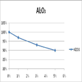
FIG. 4A is a graph showing the amount of change in color temperature according to the content of Al 2 O 3 in the
Similar to FIGS. 3A and 3B, FIGS. 4A and 4B show variations in color temperature and reduction in luminous flux with respect to weight% of Al 2 O 3 . Referring to FIG. 4A, it can be seen that? CCT decreases linearly as the% by weight of Al 2 O 3 increases. However, referring to FIG. 4B, the rate at which the luminous flux falls is represented by the weight percentage of Al 2 O 3 , and the luminous flux also decreases linearly as the weight percentage of Al 2 O 3 increases. Therefore, it is necessary to relate to the decrease of the color temperature deviation (? CCT) and the decrease of the luminous flux, and accordingly, when the Al 2 O 3 has the weight percentage of 1% to 3%, the loss of the luminous flux I can confirm that it is not wearing.
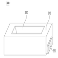
5 is a cross-sectional view illustrating a light emitting
5, the light emitting
The
The inner surface of the
The
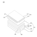
6A and 6B, the light emitting
The
The inner surface of the
The shape of the cavity formed in the
The
The phosphor (not shown) may be selected according to the wavelength of the light emitted from the
The fluorescent material (not shown) included in the
The phosphor (not shown) may be excited by the light having the first light emitted from the
When the
The phosphor (not shown) may be a known one such as YAG, TAG, sulfide, silicate, aluminate, nitride, carbide, nitridosilicate, borate, fluoride or phosphate.
The
The
The
The
The
The
The light emitting
The
The reliability of the light emitting
A light guide plate, a prism sheet, a diffusion sheet, and the like, which are optical members, may be disposed on a light path of the light emitting
The light emitting
FIG. 7A is a perspective view showing an illumination system including a light emitting device according to an embodiment, and FIG. 7B is a cross-sectional view showing a D-D 'cross section of the illumination system of FIG. 7A.
7B is a cross-sectional view of the
7A and 7B, the
The light emitting device module 543 is coupled to the lower surface of the
The light emitting device package 544 includes a lens portion (not shown) and a second region where a light emitting device (not shown) is disposed is formed to be thicker than the first region, thereby maximizing lateral light emission. Further, by using the lens portion, the light extraction efficiency of the light emitting device package 544 and the
The light emitting device package 544 is mounted on the substrate 542 in a multi-color, multi-row manner to form a module. The light emitting device package 544 can be mounted at equal intervals or can be mounted with various spacing distances as required. As the substrate 542, MCPCB (Metal Core PCB) or FR4 PCB can be used.
The
The
The light generated from the light emitting device package 544 is emitted to the outside through the
The finishing
8 is an exploded perspective view of a liquid crystal display device including a light emitting device according to an embodiment.
8, the
The liquid
The color filter substrate 612 can realize the color of an image to be displayed through the liquid
The thin
The thin
The
The light emitting device module 620 may include a
The light emitting device package 644 includes a lens unit (not shown), and the second area where the light emitting device (not shown) is disposed is formed to be thicker than the first area, thereby maximizing lateral light emission. Further, by using the lens portion, the light extraction efficiency of the
The
9 is an exploded perspective view of a liquid crystal display device including a light emitting device according to an embodiment. However, the parts shown and described in Fig. 8 are not repeatedly described in detail.
9, the liquid crystal display device 700 may include a liquid crystal display panel 710 and a backlight unit 770 for providing light to the liquid crystal display panel 710 in a direct-down manner.
Since the liquid crystal display panel 710 is the same as that described in FIG. 8, detailed description is omitted.
The backlight unit 770 includes a plurality of light emitting element modules 723, a reflective sheet 724, a lower chassis 730 in which the light emitting element module 723 and the reflective sheet 724 are accommodated, And a plurality of optical films 760 disposed on the diffuser plate 740. [
The light emitting device module 723 may include a PCB substrate 721 to mount a plurality of light emitting device packages 722 and a plurality of light emitting device packages 722 to form a module.
The light emitting device package 722 includes a lens unit (not shown), and a second region in which a light emitting device (not shown) is disposed is formed to be thicker than the first region, thereby maximizing lateral light emission. Further, by using a lens unit (not shown), the light extraction efficiency of the backlight unit 770 can be improved and the reliability of the backlight unit 770 can be further improved.
The reflective sheet 724 reflects light generated from the light emitting device package 722 in a direction in which the liquid crystal display panel 710 is positioned, thereby improving light utilization efficiency.
The light generated from the light emitting element module 723 is incident on the diffusion plate 740 and the optical film 760 is disposed on the diffusion plate 740. The optical film 760 is composed of a diffusion film 766, a prism film 750, and a protective film 764.
The configuration and the method of the embodiments described above are not limitedly applied, but the embodiments may be modified so that all or some of the embodiments are selectively combined so that various modifications can be made. .
While the present invention has been particularly shown and described with reference to exemplary embodiments thereof, it is to be understood that the invention is not limited to the disclosed exemplary embodiments, but, on the contrary, It should be understood that various modifications may be made by those skilled in the art without departing from the spirit and scope of the present invention.
10: substrate
30: Light emitting element
50: Molding agent
70: Diffusing agent
100: Light emitting device package
110: Body
130: Light emitting element
150: Molding agent
170: Diffusing agent
200: Light emitting device package
Claims (3)
A light emitting element mounted on the substrate;
A molding agent formed on the substrate and the light emitting element;
A diffusion agent contained in the molding agent; And
Wherein the diffusing agent is SiO 2 and the weight% is 0.4% or more and 1.4% or less, or the diffusing agent is Al 2 O 3 and the weight% is 1% or more and 3% or less.
Wherein the molding material is formed in a lens shape or a dome shape.
Wherein the diffusing agent is randomly distributed in the molding material.
Priority Applications (1)
| Application Number | Priority Date | Filing Date | Title |
|---|---|---|---|
| KR1020120145408A KR20140076880A (en) | 2012-12-13 | 2012-12-13 | Light Emitting Devices package |
Applications Claiming Priority (1)
| Application Number | Priority Date | Filing Date | Title |
|---|---|---|---|
| KR1020120145408A KR20140076880A (en) | 2012-12-13 | 2012-12-13 | Light Emitting Devices package |
Publications (1)
| Publication Number | Publication Date |
|---|---|
| KR20140076880A true KR20140076880A (en) | 2014-06-23 |
Family
ID=51129015
Family Applications (1)
| Application Number | Title | Priority Date | Filing Date |
|---|---|---|---|
| KR1020120145408A KR20140076880A (en) | 2012-12-13 | 2012-12-13 | Light Emitting Devices package |
Country Status (1)
| Country | Link |
|---|---|
| KR (1) | KR20140076880A (en) |
-
2012
- 2012-12-13 KR KR1020120145408A patent/KR20140076880A/en not_active Application Discontinuation
Similar Documents
| Publication | Publication Date | Title |
|---|---|---|
| US9231166B2 (en) | Light emitting device and lighting apparatus having the same | |
| KR101925915B1 (en) | Light emitting device | |
| TW201306328A (en) | Light emitting device package and lighting system using the same | |
| US8053805B2 (en) | Light emitting device, light emitting device and package, and lighting system | |
| KR101813495B1 (en) | Light Emitting Diode Package | |
| KR101641860B1 (en) | Light-emitting element array, Backlight apparatus, and Illumination apparatus | |
| TW201445774A (en) | Phosphor and light emitting device package including the same | |
| KR101694175B1 (en) | Light emitting device, Light emitting device package and Lighting system | |
| KR20140101130A (en) | Ltght emitting device | |
| KR20130140417A (en) | Light emitting device and method for fabricating the same | |
| KR101824886B1 (en) | Light emitting device package | |
| KR20140096652A (en) | Light emitting device | |
| KR101831283B1 (en) | Light Emitting Diode Package | |
| KR101818753B1 (en) | Light emitting device | |
| KR101039979B1 (en) | Light emitting device package and lighting system | |
| KR20140124063A (en) | Light emitting device | |
| KR101986720B1 (en) | Light emitting device | |
| KR20140090282A (en) | Light emitting device | |
| KR102119817B1 (en) | Light emitting device | |
| KR101883342B1 (en) | Light emitting device package | |
| KR101831329B1 (en) | Light emitting device | |
| KR20140076880A (en) | Light Emitting Devices package | |
| KR20140115655A (en) | Light emitting device | |
| KR20140099683A (en) | Light Emitting Devices package | |
| KR101983349B1 (en) | Light emitting device and manufacturing method thereof |
Legal Events
| Date | Code | Title | Description |
|---|---|---|---|
| E902 | Notification of reason for refusal | ||
| E601 | Decision to refuse application |