JP7265820B2 - Optical stacks for switchable directional displays - Google Patents
Optical stacks for switchable directional displays Download PDFInfo
- Publication number
- JP7265820B2 JP7265820B2 JP2020509511A JP2020509511A JP7265820B2 JP 7265820 B2 JP7265820 B2 JP 7265820B2 JP 2020509511 A JP2020509511 A JP 2020509511A JP 2020509511 A JP2020509511 A JP 2020509511A JP 7265820 B2 JP7265820 B2 JP 7265820B2
- Authority
- JP
- Japan
- Prior art keywords
- retarder
- liquid crystal
- polarizer
- switchable
- passive
- Prior art date
- Legal status (The legal status is an assumption and is not a legal conclusion. Google has not performed a legal analysis and makes no representation as to the accuracy of the status listed.)
- Active
Links
- 230000003287 optical effect Effects 0.000 title claims description 120
- 239000004973 liquid crystal related substance Substances 0.000 claims description 323
- 239000000463 material Substances 0.000 claims description 129
- 230000005540 biological transmission Effects 0.000 claims description 102
- 238000003384 imaging method Methods 0.000 claims description 15
- 238000000605 extraction Methods 0.000 claims description 13
- 230000004044 response Effects 0.000 claims description 3
- 238000010586 diagram Methods 0.000 description 142
- 230000010287 polarization Effects 0.000 description 96
- 238000005286 illumination Methods 0.000 description 41
- 239000000758 substrate Substances 0.000 description 39
- 230000008859 change Effects 0.000 description 22
- 210000002858 crystal cell Anatomy 0.000 description 14
- 230000000694 effects Effects 0.000 description 13
- 239000010408 film Substances 0.000 description 13
- 230000010363 phase shift Effects 0.000 description 11
- 230000009467 reduction Effects 0.000 description 8
- 230000001154 acute effect Effects 0.000 description 6
- 210000004027 cell Anatomy 0.000 description 6
- 238000009826 distribution Methods 0.000 description 5
- 229920000515 polycarbonate Polymers 0.000 description 4
- 239000004417 polycarbonate Substances 0.000 description 4
- 230000001902 propagating effect Effects 0.000 description 4
- 230000000007 visual effect Effects 0.000 description 4
- 230000008878 coupling Effects 0.000 description 3
- 238000010168 coupling process Methods 0.000 description 3
- 238000005859 coupling reaction Methods 0.000 description 3
- 239000006185 dispersion Substances 0.000 description 3
- 239000011521 glass Substances 0.000 description 3
- 229920000089 Cyclic olefin copolymer Polymers 0.000 description 2
- 239000004985 Discotic Liquid Crystal Substance Substances 0.000 description 2
- 230000015556 catabolic process Effects 0.000 description 2
- 238000006731 degradation reaction Methods 0.000 description 2
- 230000005684 electric field Effects 0.000 description 2
- 238000005516 engineering process Methods 0.000 description 2
- 238000002955 isolation Methods 0.000 description 2
- 238000004519 manufacturing process Methods 0.000 description 2
- 238000000034 method Methods 0.000 description 2
- 238000011084 recovery Methods 0.000 description 2
- 239000005268 rod-like liquid crystal Substances 0.000 description 2
- 238000009736 wetting Methods 0.000 description 2
- 239000004642 Polyimide Substances 0.000 description 1
- 238000010009 beating Methods 0.000 description 1
- 230000008033 biological extinction Effects 0.000 description 1
- 239000003086 colorant Substances 0.000 description 1
- 230000000052 comparative effect Effects 0.000 description 1
- 238000010276 construction Methods 0.000 description 1
- 230000001419 dependent effect Effects 0.000 description 1
- 238000001514 detection method Methods 0.000 description 1
- 238000009792 diffusion process Methods 0.000 description 1
- 238000002845 discoloration Methods 0.000 description 1
- 238000002474 experimental method Methods 0.000 description 1
- 230000006870 function Effects 0.000 description 1
- 230000003993 interaction Effects 0.000 description 1
- 239000005001 laminate film Substances 0.000 description 1
- 238000003475 lamination Methods 0.000 description 1
- 239000012788 optical film Substances 0.000 description 1
- 238000009304 pastoral farming Methods 0.000 description 1
- 238000000059 patterning Methods 0.000 description 1
- 230000002093 peripheral effect Effects 0.000 description 1
- 229920001721 polyimide Polymers 0.000 description 1
- 229920000642 polymer Polymers 0.000 description 1
- 229920006254 polymer film Polymers 0.000 description 1
- 229920000307 polymer substrate Polymers 0.000 description 1
- 238000003825 pressing Methods 0.000 description 1
- 230000000644 propagated effect Effects 0.000 description 1
- 238000004064 recycling Methods 0.000 description 1
- 230000035945 sensitivity Effects 0.000 description 1
- 238000004088 simulation Methods 0.000 description 1
Images


Classifications
-
- G—PHYSICS
- G02—OPTICS
- G02F—OPTICAL DEVICES OR ARRANGEMENTS FOR THE CONTROL OF LIGHT BY MODIFICATION OF THE OPTICAL PROPERTIES OF THE MEDIA OF THE ELEMENTS INVOLVED THEREIN; NON-LINEAR OPTICS; FREQUENCY-CHANGING OF LIGHT; OPTICAL LOGIC ELEMENTS; OPTICAL ANALOGUE/DIGITAL CONVERTERS
- G02F1/00—Devices or arrangements for the control of the intensity, colour, phase, polarisation or direction of light arriving from an independent light source, e.g. switching, gating or modulating; Non-linear optics
- G02F1/01—Devices or arrangements for the control of the intensity, colour, phase, polarisation or direction of light arriving from an independent light source, e.g. switching, gating or modulating; Non-linear optics for the control of the intensity, phase, polarisation or colour
- G02F1/13—Devices or arrangements for the control of the intensity, colour, phase, polarisation or direction of light arriving from an independent light source, e.g. switching, gating or modulating; Non-linear optics for the control of the intensity, phase, polarisation or colour based on liquid crystals, e.g. single liquid crystal display cells
- G02F1/133—Constructional arrangements; Operation of liquid crystal cells; Circuit arrangements
- G02F1/1333—Constructional arrangements; Manufacturing methods
- G02F1/1335—Structural association of cells with optical devices, e.g. polarisers or reflectors
- G02F1/13363—Birefringent elements, e.g. for optical compensation
-
- G—PHYSICS
- G02—OPTICS
- G02B—OPTICAL ELEMENTS, SYSTEMS OR APPARATUS
- G02B5/00—Optical elements other than lenses
- G02B5/30—Polarising elements
- G02B5/3016—Polarising elements involving passive liquid crystal elements
-
- G—PHYSICS
- G02—OPTICS
- G02B—OPTICAL ELEMENTS, SYSTEMS OR APPARATUS
- G02B5/00—Optical elements other than lenses
- G02B5/30—Polarising elements
- G02B5/3083—Birefringent or phase retarding elements
-
- G—PHYSICS
- G02—OPTICS
- G02B—OPTICAL ELEMENTS, SYSTEMS OR APPARATUS
- G02B6/00—Light guides; Structural details of arrangements comprising light guides and other optical elements, e.g. couplings
- G02B6/0001—Light guides; Structural details of arrangements comprising light guides and other optical elements, e.g. couplings specially adapted for lighting devices or systems
- G02B6/0011—Light guides; Structural details of arrangements comprising light guides and other optical elements, e.g. couplings specially adapted for lighting devices or systems the light guides being planar or of plate-like form
- G02B6/0033—Means for improving the coupling-out of light from the light guide
- G02B6/0035—Means for improving the coupling-out of light from the light guide provided on the surface of the light guide or in the bulk of it
-
- G—PHYSICS
- G02—OPTICS
- G02B—OPTICAL ELEMENTS, SYSTEMS OR APPARATUS
- G02B6/00—Light guides; Structural details of arrangements comprising light guides and other optical elements, e.g. couplings
- G02B6/0001—Light guides; Structural details of arrangements comprising light guides and other optical elements, e.g. couplings specially adapted for lighting devices or systems
- G02B6/0011—Light guides; Structural details of arrangements comprising light guides and other optical elements, e.g. couplings specially adapted for lighting devices or systems the light guides being planar or of plate-like form
- G02B6/0033—Means for improving the coupling-out of light from the light guide
- G02B6/005—Means for improving the coupling-out of light from the light guide provided by one optical element, or plurality thereof, placed on the light output side of the light guide
- G02B6/0055—Reflecting element, sheet or layer
-
- G—PHYSICS
- G02—OPTICS
- G02F—OPTICAL DEVICES OR ARRANGEMENTS FOR THE CONTROL OF LIGHT BY MODIFICATION OF THE OPTICAL PROPERTIES OF THE MEDIA OF THE ELEMENTS INVOLVED THEREIN; NON-LINEAR OPTICS; FREQUENCY-CHANGING OF LIGHT; OPTICAL LOGIC ELEMENTS; OPTICAL ANALOGUE/DIGITAL CONVERTERS
- G02F1/00—Devices or arrangements for the control of the intensity, colour, phase, polarisation or direction of light arriving from an independent light source, e.g. switching, gating or modulating; Non-linear optics
- G02F1/01—Devices or arrangements for the control of the intensity, colour, phase, polarisation or direction of light arriving from an independent light source, e.g. switching, gating or modulating; Non-linear optics for the control of the intensity, phase, polarisation or colour
- G02F1/13—Devices or arrangements for the control of the intensity, colour, phase, polarisation or direction of light arriving from an independent light source, e.g. switching, gating or modulating; Non-linear optics for the control of the intensity, phase, polarisation or colour based on liquid crystals, e.g. single liquid crystal display cells
- G02F1/1323—Arrangements for providing a switchable viewing angle
-
- G—PHYSICS
- G02—OPTICS
- G02F—OPTICAL DEVICES OR ARRANGEMENTS FOR THE CONTROL OF LIGHT BY MODIFICATION OF THE OPTICAL PROPERTIES OF THE MEDIA OF THE ELEMENTS INVOLVED THEREIN; NON-LINEAR OPTICS; FREQUENCY-CHANGING OF LIGHT; OPTICAL LOGIC ELEMENTS; OPTICAL ANALOGUE/DIGITAL CONVERTERS
- G02F1/00—Devices or arrangements for the control of the intensity, colour, phase, polarisation or direction of light arriving from an independent light source, e.g. switching, gating or modulating; Non-linear optics
- G02F1/01—Devices or arrangements for the control of the intensity, colour, phase, polarisation or direction of light arriving from an independent light source, e.g. switching, gating or modulating; Non-linear optics for the control of the intensity, phase, polarisation or colour
- G02F1/13—Devices or arrangements for the control of the intensity, colour, phase, polarisation or direction of light arriving from an independent light source, e.g. switching, gating or modulating; Non-linear optics for the control of the intensity, phase, polarisation or colour based on liquid crystals, e.g. single liquid crystal display cells
- G02F1/133—Constructional arrangements; Operation of liquid crystal cells; Circuit arrangements
- G02F1/1333—Constructional arrangements; Manufacturing methods
- G02F1/1335—Structural association of cells with optical devices, e.g. polarisers or reflectors
- G02F1/133528—Polarisers
- G02F1/133536—Reflective polarizers
-
- G—PHYSICS
- G02—OPTICS
- G02F—OPTICAL DEVICES OR ARRANGEMENTS FOR THE CONTROL OF LIGHT BY MODIFICATION OF THE OPTICAL PROPERTIES OF THE MEDIA OF THE ELEMENTS INVOLVED THEREIN; NON-LINEAR OPTICS; FREQUENCY-CHANGING OF LIGHT; OPTICAL LOGIC ELEMENTS; OPTICAL ANALOGUE/DIGITAL CONVERTERS
- G02F1/00—Devices or arrangements for the control of the intensity, colour, phase, polarisation or direction of light arriving from an independent light source, e.g. switching, gating or modulating; Non-linear optics
- G02F1/01—Devices or arrangements for the control of the intensity, colour, phase, polarisation or direction of light arriving from an independent light source, e.g. switching, gating or modulating; Non-linear optics for the control of the intensity, phase, polarisation or colour
- G02F1/13—Devices or arrangements for the control of the intensity, colour, phase, polarisation or direction of light arriving from an independent light source, e.g. switching, gating or modulating; Non-linear optics for the control of the intensity, phase, polarisation or colour based on liquid crystals, e.g. single liquid crystal display cells
- G02F1/133—Constructional arrangements; Operation of liquid crystal cells; Circuit arrangements
- G02F1/1333—Constructional arrangements; Manufacturing methods
- G02F1/1335—Structural association of cells with optical devices, e.g. polarisers or reflectors
- G02F1/13363—Birefringent elements, e.g. for optical compensation
- G02F1/133634—Birefringent elements, e.g. for optical compensation the refractive index Nz perpendicular to the element surface being different from in-plane refractive indices Nx and Ny, e.g. biaxial or with normal optical axis
-
- G—PHYSICS
- G02—OPTICS
- G02F—OPTICAL DEVICES OR ARRANGEMENTS FOR THE CONTROL OF LIGHT BY MODIFICATION OF THE OPTICAL PROPERTIES OF THE MEDIA OF THE ELEMENTS INVOLVED THEREIN; NON-LINEAR OPTICS; FREQUENCY-CHANGING OF LIGHT; OPTICAL LOGIC ELEMENTS; OPTICAL ANALOGUE/DIGITAL CONVERTERS
- G02F1/00—Devices or arrangements for the control of the intensity, colour, phase, polarisation or direction of light arriving from an independent light source, e.g. switching, gating or modulating; Non-linear optics
- G02F1/01—Devices or arrangements for the control of the intensity, colour, phase, polarisation or direction of light arriving from an independent light source, e.g. switching, gating or modulating; Non-linear optics for the control of the intensity, phase, polarisation or colour
- G02F1/13—Devices or arrangements for the control of the intensity, colour, phase, polarisation or direction of light arriving from an independent light source, e.g. switching, gating or modulating; Non-linear optics for the control of the intensity, phase, polarisation or colour based on liquid crystals, e.g. single liquid crystal display cells
- G02F1/133—Constructional arrangements; Operation of liquid crystal cells; Circuit arrangements
- G02F1/1333—Constructional arrangements; Manufacturing methods
- G02F1/1337—Surface-induced orientation of the liquid crystal molecules, e.g. by alignment layers
-
- G—PHYSICS
- G02—OPTICS
- G02F—OPTICAL DEVICES OR ARRANGEMENTS FOR THE CONTROL OF LIGHT BY MODIFICATION OF THE OPTICAL PROPERTIES OF THE MEDIA OF THE ELEMENTS INVOLVED THEREIN; NON-LINEAR OPTICS; FREQUENCY-CHANGING OF LIGHT; OPTICAL LOGIC ELEMENTS; OPTICAL ANALOGUE/DIGITAL CONVERTERS
- G02F1/00—Devices or arrangements for the control of the intensity, colour, phase, polarisation or direction of light arriving from an independent light source, e.g. switching, gating or modulating; Non-linear optics
- G02F1/01—Devices or arrangements for the control of the intensity, colour, phase, polarisation or direction of light arriving from an independent light source, e.g. switching, gating or modulating; Non-linear optics for the control of the intensity, phase, polarisation or colour
- G02F1/13—Devices or arrangements for the control of the intensity, colour, phase, polarisation or direction of light arriving from an independent light source, e.g. switching, gating or modulating; Non-linear optics for the control of the intensity, phase, polarisation or colour based on liquid crystals, e.g. single liquid crystal display cells
- G02F1/133—Constructional arrangements; Operation of liquid crystal cells; Circuit arrangements
- G02F1/1333—Constructional arrangements; Manufacturing methods
- G02F1/1347—Arrangement of liquid crystal layers or cells in which the final condition of one light beam is achieved by the addition of the effects of two or more layers or cells
- G02F1/13471—Arrangement of liquid crystal layers or cells in which the final condition of one light beam is achieved by the addition of the effects of two or more layers or cells in which all the liquid crystal cells or layers remain transparent, e.g. FLC, ECB, DAP, HAN, TN, STN, SBE-LC cells
-
- G—PHYSICS
- G02—OPTICS
- G02F—OPTICAL DEVICES OR ARRANGEMENTS FOR THE CONTROL OF LIGHT BY MODIFICATION OF THE OPTICAL PROPERTIES OF THE MEDIA OF THE ELEMENTS INVOLVED THEREIN; NON-LINEAR OPTICS; FREQUENCY-CHANGING OF LIGHT; OPTICAL LOGIC ELEMENTS; OPTICAL ANALOGUE/DIGITAL CONVERTERS
- G02F1/00—Devices or arrangements for the control of the intensity, colour, phase, polarisation or direction of light arriving from an independent light source, e.g. switching, gating or modulating; Non-linear optics
- G02F1/01—Devices or arrangements for the control of the intensity, colour, phase, polarisation or direction of light arriving from an independent light source, e.g. switching, gating or modulating; Non-linear optics for the control of the intensity, phase, polarisation or colour
- G02F1/13—Devices or arrangements for the control of the intensity, colour, phase, polarisation or direction of light arriving from an independent light source, e.g. switching, gating or modulating; Non-linear optics for the control of the intensity, phase, polarisation or colour based on liquid crystals, e.g. single liquid crystal display cells
- G02F1/137—Devices or arrangements for the control of the intensity, colour, phase, polarisation or direction of light arriving from an independent light source, e.g. switching, gating or modulating; Non-linear optics for the control of the intensity, phase, polarisation or colour based on liquid crystals, e.g. single liquid crystal display cells characterised by the electro-optical or magneto-optical effect, e.g. field-induced phase transition, orientation effect, guest-host interaction or dynamic scattering
-
- G—PHYSICS
- G02—OPTICS
- G02F—OPTICAL DEVICES OR ARRANGEMENTS FOR THE CONTROL OF LIGHT BY MODIFICATION OF THE OPTICAL PROPERTIES OF THE MEDIA OF THE ELEMENTS INVOLVED THEREIN; NON-LINEAR OPTICS; FREQUENCY-CHANGING OF LIGHT; OPTICAL LOGIC ELEMENTS; OPTICAL ANALOGUE/DIGITAL CONVERTERS
- G02F1/00—Devices or arrangements for the control of the intensity, colour, phase, polarisation or direction of light arriving from an independent light source, e.g. switching, gating or modulating; Non-linear optics
- G02F1/01—Devices or arrangements for the control of the intensity, colour, phase, polarisation or direction of light arriving from an independent light source, e.g. switching, gating or modulating; Non-linear optics for the control of the intensity, phase, polarisation or colour
- G02F1/13—Devices or arrangements for the control of the intensity, colour, phase, polarisation or direction of light arriving from an independent light source, e.g. switching, gating or modulating; Non-linear optics for the control of the intensity, phase, polarisation or colour based on liquid crystals, e.g. single liquid crystal display cells
- G02F1/133—Constructional arrangements; Operation of liquid crystal cells; Circuit arrangements
- G02F1/1333—Constructional arrangements; Manufacturing methods
- G02F1/1337—Surface-induced orientation of the liquid crystal molecules, e.g. by alignment layers
- G02F1/133738—Surface-induced orientation of the liquid crystal molecules, e.g. by alignment layers for homogeneous alignment
-
- G—PHYSICS
- G02—OPTICS
- G02F—OPTICAL DEVICES OR ARRANGEMENTS FOR THE CONTROL OF LIGHT BY MODIFICATION OF THE OPTICAL PROPERTIES OF THE MEDIA OF THE ELEMENTS INVOLVED THEREIN; NON-LINEAR OPTICS; FREQUENCY-CHANGING OF LIGHT; OPTICAL LOGIC ELEMENTS; OPTICAL ANALOGUE/DIGITAL CONVERTERS
- G02F1/00—Devices or arrangements for the control of the intensity, colour, phase, polarisation or direction of light arriving from an independent light source, e.g. switching, gating or modulating; Non-linear optics
- G02F1/01—Devices or arrangements for the control of the intensity, colour, phase, polarisation or direction of light arriving from an independent light source, e.g. switching, gating or modulating; Non-linear optics for the control of the intensity, phase, polarisation or colour
- G02F1/13—Devices or arrangements for the control of the intensity, colour, phase, polarisation or direction of light arriving from an independent light source, e.g. switching, gating or modulating; Non-linear optics for the control of the intensity, phase, polarisation or colour based on liquid crystals, e.g. single liquid crystal display cells
- G02F1/133—Constructional arrangements; Operation of liquid crystal cells; Circuit arrangements
- G02F1/1333—Constructional arrangements; Manufacturing methods
- G02F1/1337—Surface-induced orientation of the liquid crystal molecules, e.g. by alignment layers
- G02F1/133742—Surface-induced orientation of the liquid crystal molecules, e.g. by alignment layers for homeotropic alignment
-
- G—PHYSICS
- G02—OPTICS
- G02F—OPTICAL DEVICES OR ARRANGEMENTS FOR THE CONTROL OF LIGHT BY MODIFICATION OF THE OPTICAL PROPERTIES OF THE MEDIA OF THE ELEMENTS INVOLVED THEREIN; NON-LINEAR OPTICS; FREQUENCY-CHANGING OF LIGHT; OPTICAL LOGIC ELEMENTS; OPTICAL ANALOGUE/DIGITAL CONVERTERS
- G02F1/00—Devices or arrangements for the control of the intensity, colour, phase, polarisation or direction of light arriving from an independent light source, e.g. switching, gating or modulating; Non-linear optics
- G02F1/01—Devices or arrangements for the control of the intensity, colour, phase, polarisation or direction of light arriving from an independent light source, e.g. switching, gating or modulating; Non-linear optics for the control of the intensity, phase, polarisation or colour
- G02F1/13—Devices or arrangements for the control of the intensity, colour, phase, polarisation or direction of light arriving from an independent light source, e.g. switching, gating or modulating; Non-linear optics for the control of the intensity, phase, polarisation or colour based on liquid crystals, e.g. single liquid crystal display cells
- G02F1/137—Devices or arrangements for the control of the intensity, colour, phase, polarisation or direction of light arriving from an independent light source, e.g. switching, gating or modulating; Non-linear optics for the control of the intensity, phase, polarisation or colour based on liquid crystals, e.g. single liquid crystal display cells characterised by the electro-optical or magneto-optical effect, e.g. field-induced phase transition, orientation effect, guest-host interaction or dynamic scattering
- G02F1/13706—Devices or arrangements for the control of the intensity, colour, phase, polarisation or direction of light arriving from an independent light source, e.g. switching, gating or modulating; Non-linear optics for the control of the intensity, phase, polarisation or colour based on liquid crystals, e.g. single liquid crystal display cells characterised by the electro-optical or magneto-optical effect, e.g. field-induced phase transition, orientation effect, guest-host interaction or dynamic scattering the liquid crystal having positive dielectric anisotropy
-
- G—PHYSICS
- G02—OPTICS
- G02F—OPTICAL DEVICES OR ARRANGEMENTS FOR THE CONTROL OF LIGHT BY MODIFICATION OF THE OPTICAL PROPERTIES OF THE MEDIA OF THE ELEMENTS INVOLVED THEREIN; NON-LINEAR OPTICS; FREQUENCY-CHANGING OF LIGHT; OPTICAL LOGIC ELEMENTS; OPTICAL ANALOGUE/DIGITAL CONVERTERS
- G02F1/00—Devices or arrangements for the control of the intensity, colour, phase, polarisation or direction of light arriving from an independent light source, e.g. switching, gating or modulating; Non-linear optics
- G02F1/01—Devices or arrangements for the control of the intensity, colour, phase, polarisation or direction of light arriving from an independent light source, e.g. switching, gating or modulating; Non-linear optics for the control of the intensity, phase, polarisation or colour
- G02F1/13—Devices or arrangements for the control of the intensity, colour, phase, polarisation or direction of light arriving from an independent light source, e.g. switching, gating or modulating; Non-linear optics for the control of the intensity, phase, polarisation or colour based on liquid crystals, e.g. single liquid crystal display cells
- G02F1/137—Devices or arrangements for the control of the intensity, colour, phase, polarisation or direction of light arriving from an independent light source, e.g. switching, gating or modulating; Non-linear optics for the control of the intensity, phase, polarisation or colour based on liquid crystals, e.g. single liquid crystal display cells characterised by the electro-optical or magneto-optical effect, e.g. field-induced phase transition, orientation effect, guest-host interaction or dynamic scattering
- G02F1/13712—Devices or arrangements for the control of the intensity, colour, phase, polarisation or direction of light arriving from an independent light source, e.g. switching, gating or modulating; Non-linear optics for the control of the intensity, phase, polarisation or colour based on liquid crystals, e.g. single liquid crystal display cells characterised by the electro-optical or magneto-optical effect, e.g. field-induced phase transition, orientation effect, guest-host interaction or dynamic scattering the liquid crystal having negative dielectric anisotropy
-
- G—PHYSICS
- G02—OPTICS
- G02F—OPTICAL DEVICES OR ARRANGEMENTS FOR THE CONTROL OF LIGHT BY MODIFICATION OF THE OPTICAL PROPERTIES OF THE MEDIA OF THE ELEMENTS INVOLVED THEREIN; NON-LINEAR OPTICS; FREQUENCY-CHANGING OF LIGHT; OPTICAL LOGIC ELEMENTS; OPTICAL ANALOGUE/DIGITAL CONVERTERS
- G02F2203/00—Function characteristic
- G02F2203/12—Function characteristic spatial light modulator
-
- G—PHYSICS
- G02—OPTICS
- G02F—OPTICAL DEVICES OR ARRANGEMENTS FOR THE CONTROL OF LIGHT BY MODIFICATION OF THE OPTICAL PROPERTIES OF THE MEDIA OF THE ELEMENTS INVOLVED THEREIN; NON-LINEAR OPTICS; FREQUENCY-CHANGING OF LIGHT; OPTICAL LOGIC ELEMENTS; OPTICAL ANALOGUE/DIGITAL CONVERTERS
- G02F2413/00—Indexing scheme related to G02F1/13363, i.e. to birefringent elements, e.g. for optical compensation, characterised by the number, position, orientation or value of the compensation plates
- G02F2413/02—Number of plates being 2
Description
本開示は、概して、光変調素子からの照明に関し、より具体的には、プライバシーディスプレイなどディスプレイで用いる照明を制御するための切り替え可能な光学積層体に関する。 TECHNICAL FIELD This disclosure relates generally to illumination from light modulating elements, and more particularly to switchable optical stacks for controlling illumination for use in displays such as privacy displays.
プライバシーディスプレイは、典型的に軸上位置にいる主たるユーザには画像視認性をもたらし、典型的に軸外位置にいるスヌーパーに対する画像コンテンツの視認性を低減する。プライバシー機能は、軸上方向のディスプレイからの一部の光を透過し、軸外位置では低輝度である、マイクロルーバー光学フィルムによって提供され得る。しかしながら、かかるフィルムは、正面からの照明に対して高損失であり、マイクロルーバーは、空間光変調器の画素のビートを原因とするモアレを生じさせる場合がある。マイクロルーバーのピッチは、パネル解像度の選択に応じて選択する必要があり、在庫及びコストを増加させ得る。 Privacy displays provide image visibility to primary users, who are typically on-axis, and reduce visibility of image content to snoopers, who are typically off-axis. A privacy feature can be provided by a microlouver optical film that transmits some light from the display in on-axis directions and has low brightness in off-axis positions. However, such films are highly lossy for head-on illumination, and microlouvers can cause moire due to spatial light modulator pixel beating. The microlouver pitch must be selected according to the panel resolution choice, which can increase inventory and cost.
切り替え可能なプライバシーディスプレイは、軸外光出力の制御によってもたらされ得る。 A switchable privacy display can be provided by controlling off-axis light output.
制御は、例えば液晶ディスプレイ(LCD)空間光変調器の切り替え可能なバックライトによる輝度の低下によってもたらされ得る。ディスプレイのバックライトは、概して導波路及び端部発光源を用いる。特定の結像指向性バックライトは、ディスプレイパネルを通して照明を視野窓に方向付ける追加機能を有する。結像システムは、複数の光源とそれぞれの窓画像との間に形成することができる。結像指向性バックライトの1つの例として折りたたみ式光学システムを用いることができる光弁が挙げられ、したがってこれは、折りたたみ式結像指向性バックライトの1つの例でもあり得る。光は実質的に、光弁を通して一方向に損失を伴わずに伝搬することができ、同時に対向伝搬光は、参照によりその全体が本明細書に組み込まれる米国特許第9,519,153号に記述されるように、反射傾斜ファセットによって抽出することができる。 Control may be provided, for example, by reducing brightness with a switchable backlight of a liquid crystal display (LCD) spatial light modulator. Display backlights typically use waveguides and edge emitting sources. Certain imaging directional backlights have the additional function of directing illumination through the display panel to a viewing window. An imaging system can be formed between the plurality of light sources and respective window images. One example of an imaging directional backlight is a light valve that can use a folding optical system, so it can also be an example of a folding imaging directional backlight. Light can be substantially losslessly propagated through the light valve in one direction while counter-propagating light is described in U.S. Pat. As described, it can be extracted by reflective tilted facets.
軸外プライバシーの制御は、例えば、インプレーンスイッチングLCDでの液晶バイアス傾斜の調整によるコントラストの低減によって更にもたらされ得る。 Off-axis privacy control can be further provided by contrast reduction, for example, by adjusting the liquid crystal bias tilt in in-plane switching LCDs.
本開示の第1態様によると、空間光変調器と、空間光変調器の側に配置されたディスプレイ偏光子と、ディスプレイ偏光子と同じ空間光変調器の側に配置された追加偏光子と、追加偏光子とディスプレイ偏光子との間に配置された複数のリターダと、を備えるディスプレイ装置が提供され、複数のリターダは、ディスプレイ偏光子と追加偏光子との間に配置された液晶材料の層と、少なくとも1つの受動補償リターダと、を備える切り替え可能な液晶リターダを備える。 According to a first aspect of the present disclosure, a spatial light modulator, a display polarizer positioned on the side of the spatial light modulator, an additional polarizer positioned on the same side of the spatial light modulator as the display polarizer, and a plurality of retarders disposed between an additional polarizer and a display polarizer, the plurality of retarders being a layer of liquid crystal material disposed between the display polarizer and the additional polarizer. and at least one passive compensating retarder.
複数のリターダは、リターダの平面の法線に沿った軸に沿ってディスプレイ偏光子、追加偏光子、及び複数のリターダを通過する光の輝度に影響を及ぼさないように、及び/又はリターダの平面の法線に対して傾斜した軸に沿ってディスプレイ偏光子、追加偏光子、及び複数のリターダを通過する光の輝度を低下させるように構成されてよい。 The plurality of retarders may be arranged so as not to affect the brightness of light passing through the display polarizer, the additional polarizer, and the plurality of retarders along an axis normal to the plane of the retarders and/or the plane of the retarders. may be configured to reduce the brightness of light passing through the display polarizer, the additional polarizer, and the plurality of retarders along an axis that is tilted with respect to the normal of .
少なくとも1つの受動補償リターダは、少なくとも1つの受動補償リターダの平面の法線に沿った軸に沿って、複数のリターダの入力側のディスプレイ偏光子及び追加偏光子のうちの1つが通過する光の偏光成分に位相シフトを導入しないように、及び/又は少なくとも1つの受動補償リターダの平面の法線に対して傾斜した軸に沿って、複数のリターダの入力側のディスプレイ偏光子及び追加偏光子のうちの1つが通過する光の偏光成分に位相シフトを導入するように構成されてよい。 The at least one passive compensating retarder directs light passing through one of the display polarizer and the additional polarizer on the input side of the plurality of retarders along an axis normal to the plane of the at least one passive compensating retarder. of the display polarizer and the additional polarizer on the input side of the plurality of retarders so as not to introduce phase shifts in the polarization components and/or along axes tilted with respect to the normal to the plane of the at least one passive compensating retarder. One of them may be configured to introduce a phase shift in the polarization components of light passing through.
切り替え可能な液晶リターダは、切り替え可能な液晶リターダの平面の法線に沿った軸に沿って、複数のリターダの入力側のディスプレイ偏光子及び追加偏光子のうちの1つが通過する光の偏光成分に位相シフトを導入しないように、及び/又は切り替え可能な液晶リターダの切り替え可能状態で、切り替え可能な液晶リターダの平面の法線に対して傾斜した軸に沿って、複数のリターダの入力側のディスプレイ偏光子及び追加偏光子のうちの1つが通過する光の偏光成分に位相シフトを導入するように構成されてよい。 The switchable liquid crystal retarder directs the polarization component of light passing through one of the input side display polarizer and the additional polarizer of the plurality of retarders along an axis normal to the plane of the switchable liquid crystal retarder. and/or in the switchable state of the switchable liquid crystal retarders along an axis tilted with respect to the normal to the plane of the switchable liquid crystal retarders. One of the display polarizer and the additional polarizer may be configured to introduce a phase shift in the polarization components of the light passing therethrough.
有利なことには、広角動作状態とプライバシー動作状態とを切り替えられ得る、切り替え可能なプライバシーディスプレイが提供され得る。プライバシー動作の視野は、既知の装置と比較して拡張され得、より低い軸外輝度レベルが達成され得、軸外のスヌーパーによって観察されるプライバシーの程度を向上させ得る。更に、軸上の主たるユーザに対する軸上輝度は、広角動作状態及びプライバシー動作状態の両方において維持され得る。 Advantageously, a switchable privacy display can be provided that can be switched between a wide angle operating state and a privacy operating state. The field of view for privacy operation may be extended compared to known devices, lower off-axis luminance levels may be achieved, and the degree of privacy observed by off-axis snoopers may be enhanced. Additionally, on-axis luminance for the on-axis primary user can be maintained in both wide-angle and privacy operating conditions.
ディスプレイ偏光子及び追加偏光子は、平行の電気ベクトル伝達方向を有してよい。 The display polarizer and the additional polarizer may have parallel electric vector transmission directions.
1つの代替例では、切り替え可能な液晶リターダは、液晶材料の層に隣接し、かつその両側に配置され、隣接する液晶材料内にホメオトロピック配向をもたらすようにそれぞれ構成されている、2つの表面配向層を備えてよい。切り替え可能な液晶リターダの液晶材料の層は、負の誘電率異方性を有する液晶材料を含んでよい。液晶材料の層は、550nmの波長の光に対して500nm~1000nmの範囲、好ましくは600nm~900nmの範囲、最も好ましくは700nm~850nmの範囲のリターダンスを有してよい。
In one alternative, the switchable liquid crystal retarder is positioned adjacent to and on either side of the layer of liquid crystal material on two surfaces each configured to provide homeotropic alignment in the adjacent liquid crystal material. An alignment layer may be provided. The layer of liquid crystal material of the switchable liquid crystal retarder may comprise liquid crystal material with negative dielectric anisotropy. The layer of liquid crystal material may have a retardance for light of wavelength 550 nm in the
ホメオトロピック配向をもたらす2つの表面配向層が設けられる場合、少なくとも1つの受動補償リターダは、リターダの平面に対して垂直である光軸を有するリターダを備えてよく、少なくとも1つの受動リターダは、550nmの波長の光に対して-300nm~-900nmの範囲、好ましくは-450nm~-800nmの範囲、最も好ましくは-500nm~-725nmの範囲のリターダンスを有する。 At least one passive compensating retarder may comprise a retarder with an optic axis that is perpendicular to the plane of the retarder, if two surface alignment layers are provided that provide homeotropic alignment, and at least one passive retarder is 550 nm It has a retardance in the range of -300 nm to -900 nm, preferably in the range of -450 nm to -800 nm, most preferably in the range of -500 nm to -725 nm for light of wavelength of .
あるいは、ホメオトロピック配向をもたらす2つの表面配向層が設けられる場合、少なくとも1つの受動補償リターダは、交差するリターダの平面内に光軸を有する一対のリターダを備えてよく、この一対のリターダの各リターダは、550nmの波長の光に対して300nm~800nmの範囲、好ましくは500nm~700nmの範囲、最も好ましくは550nm~675nmの範囲のリターダンスを有する。有利なことには、この場合、広角動作モードでの視野が拡大され得る。更に、広角動作モードでのゼロ電圧動作が提供されて、電力消費を低減し得る。
Alternatively, if two surface alignment layers are provided that provide homeotropic alignment, the at least one passive compensating retarder may comprise a pair of retarders with optic axes in the planes of the intersecting retarders, each of the pair of retarders The retarder has a retardance for light of wavelength 550 nm in the
別の代替例では、切り替え可能な液晶リターダは、液晶材料の層に隣接し、かつその両側に配置され、隣接する液晶材料内にホモジニアス配向をもたらすようにそれぞれ構成されている、2つの表面配向層を備えてよい。有利なことには、液晶の両側でのホメオトロピック配向と比較して、圧力印加中の液晶材料の流動の視認性に対する回復力が向上し得る。 In another alternative, the switchable liquid crystal retarder is positioned adjacent to and on either side of the layer of liquid crystal material, with two surface alignments each configured to provide homogeneous alignment in the adjacent liquid crystal material. It may have layers. Advantageously, the visibility resilience of the liquid crystal material flow during application of pressure may be improved compared to homeotropic alignment on both sides of the liquid crystal.
切り替え可能な液晶リターダの液晶材料の層は、正の誘電率異方性を有する液晶材料を含んでよい。液晶材料の層は、550nmの波長の光に対して500nm~900nmの範囲、好ましくは600nm~850nmの範囲、最も好ましくは700nm~800nmの範囲のリターダンスを有してよい。
The layer of liquid crystal material of the switchable liquid crystal retarder may comprise liquid crystal material having a positive dielectric anisotropy. The layer of liquid crystal material may have a retardance for light of wavelength 550 nm in the
ホモジニアス配向をもたらす2つの表面配向層が設けられる場合、少なくとも1つの受動補償リターダは、リターダの平面に対して垂直である光軸を有するリターダを備えてよく、少なくとも1つの受動リターダは、550nmの波長の光に対して-300nm~-700nmの範囲、好ましくは-350nm~-600nmの範囲、最も好ましくは-400nm~-500nmの範囲のリターダンスを有する。 At least one passive compensating retarder may comprise a retarder with an optic axis that is perpendicular to the plane of the retarder, and at least one passive retarder may have a It has a retardance for wavelengths of light in the range -300 nm to -700 nm, preferably in the range -350 nm to -600 nm, most preferably in the range -400 nm to -500 nm.
あるいは、ホモジニアス配向をもたらす2つの表面配向層が設けられる場合、少なくとも1つの受動補償リターダは、交差するリターダの平面内に光軸を有する一対のリターダを備えてよく、この一対のリターダの各リターダは、550nmの波長の光に対して300nm~800nmの範囲、好ましくは350nm~650nmの範囲、最も好ましくは450nm~550nmの範囲のリターダンスを有する。有利なことには、この場合、圧力印加中の液晶材料の流動の視認性に対する回復力が向上し得る。
Alternatively, if two surface alignment layers are provided that provide homogeneous alignment, the at least one passive compensating retarder may comprise a pair of retarders with optic axes in the plane of the intersecting retarders, each retarder of the pair of retarders has a retardance for light of wavelength 550 nm in the
別の代替例では、切り替え可能な液晶リターダは、液晶材料の層に隣接し、かつその両側に配置された2つの表面配向層を備えてよく、表面配向層のうちの1つは、隣接する液晶材料内にホメオトロピック配向をもたらすように構成され、表面配向層の他方は、隣接する液晶材料内にホモジニアス配向をもたらすように構成されている。 In another alternative, the switchable liquid crystal retarder may comprise two surface alignment layers positioned adjacent to and on either side of the layer of liquid crystal material, one of the surface alignment layers being adjacent to the layer of liquid crystal material. The other of the surface alignment layers is configured to provide homeotropic alignment in the liquid crystal material and the other surface alignment layer is configured to provide homogeneous alignment in the adjacent liquid crystal material.
ホモジニアス配向をもたらすように構成されている表面配向層が液晶材料の層と補償リターダとの間にある場合、液晶材料の層は、550nmの波長の光に対して700nm~2000nmの範囲、好ましくは1000nm~1500nmの範囲、最も好ましくは1200nm~1500nmの範囲のリターダンスを有してよい。 If a surface alignment layer configured to provide homogeneous alignment is between the layer of liquid crystal material and the compensating retarder, the layer of liquid crystal material is in the range of 700 nm to 2000 nm, preferably It may have a retardance in the range 1000 nm to 1500 nm, most preferably in the range 1200 nm to 1500 nm.
ホモジニアス配向をもたらすように構成されている表面配向層が液晶材料の層と補償リターダとの間にある場合、少なくとも1つの受動補償リターダは、リターダの平面に対して垂直である光軸を有するリターダを備えてよく、少なくとも1つの受動リターダは、550nmの波長の光に対して-400nm~-1800nmの範囲、好ましくは-700nm~-1500nmの範囲、最も好ましくは-900nm~-1300nmの範囲のリターダンスを有する。 At least one passive compensating retarder is a retarder having an optic axis that is perpendicular to the plane of the retarder if a surface alignment layer configured to provide homogeneous alignment is between the layer of liquid crystal material and the compensating retarder and at least one passive retarder comprises a retarder in the range -400 nm to -1800 nm, preferably in the range -700 nm to -1500 nm, most preferably in the range -900 nm to -1300 nm for light of wavelength 550 nm. have a dance
ホモジニアス配向をもたらすように構成されている表面配向層が液晶材料の層と補償リターダとの間にある場合、少なくとも1つの受動補償リターダは、交差するリターダの平面内に光軸を有する一対のリターダを備えてよく、この一対のリターダのそれぞれは、550nmの波長の光に対して400nm~1800nmの範囲、好ましくは700nm~1500nmの範囲、最も好ましくは900nm~1300nmの範囲のリターダンスを有する。
If a surface alignment layer configured to provide homogeneous alignment is between the layer of liquid crystal material and the compensating retarder, the at least one passive compensating retarder is a pair of retarders having an optic axis in the plane of the intersecting retarders. each of the pair of retarders has a retardance for light of wavelength 550 nm in the
ホメオトロピック配向をもたらすように構成されている表面配向層が液晶材料の層と補償リターダとの間にある場合、液晶材料の層は、550nmの波長の光に対して500nm~1800nmの範囲、好ましくは700nm~1500nmの範囲、最も好ましくは900nm~1350nmの範囲のリターダンスを有してよい。
If a surface alignment layer configured to provide homeotropic alignment is between the layer of liquid crystal material and the compensating retarder, the layer of liquid crystal material is preferably in the
ホメオトロピック配向をもたらすように構成されている表面配向層が液晶材料の層と補償リターダとの間にある場合、少なくとも1つの受動補償リターダは、リターダの平面に対して垂直である光軸を有するリターダを備えてよく、少なくとも1つの受動リターダは、550nmの波長の光に対して-300nm~-1600nmの範囲、好ましくは-500nm~-1300nmの範囲、最も好ましくは-700nm~-1150nmの範囲のリターダンスを有する。 At least one passive compensating retarder has an optic axis that is perpendicular to the plane of the retarder if a surface alignment layer configured to provide homeotropic alignment is between the layer of liquid crystal material and the compensating retarder. A retarder may be provided, at least one passive retarder having a Has a retardance.
ホメオトロピック配向をもたらすように構成されている表面配向層が液晶材料の層と補償リターダとの間にある場合、少なくとも1つの受動補償リターダは、交差するリターダの平面内に光軸を有する一対のリターダを備えてよく、この一対のリターダの各リターダは、550nmの波長の光に対して400nm~1600nmの範囲、好ましくは600nm~1400nmの範囲、最も好ましくは800nm~1300nmの範囲のリターダンスを有する。有利なことには、この場合、圧力印加中の液晶材料の流動の視認性に対する回復力が向上し得る。
When a surface alignment layer configured to provide homeotropic alignment is between the layer of liquid crystal material and the compensating retarder, the at least one passive compensating retarder comprises a pair of optic axes in the plane of the intersecting retarders. A retarder may be provided, each retarder of the pair of retarders having a retardance for light of wavelength 550 nm in the
各配向層は、ディスプレイ偏光子の電気ベクトル伝達方向に対して平行若しくは逆平行である、又は直交する液晶層の平面内の成分とのプレチルト方向を有するプレチルトを有してよい。有利なことには、ディスプレイには、横方向の狭視野角、及び水平軸の周りでのディスプレイの回転に対する高視聴自由度が提供され得る。かかるディスプレイは、正面のディスプレイユーザには見やすく、軸外のディスプレイユーザには見にくいことがある。 Each alignment layer may have a pretilt with a pretilt direction with a component in the plane of the liquid crystal layer that is parallel, antiparallel, or orthogonal to the electric vector propagation direction of the display polarizers. Advantageously, the display can be provided with a narrow lateral viewing angle and high viewing freedom for rotation of the display about the horizontal axis. Such displays may be easy to see for front display users and difficult for off-axis display users.
少なくとも1つの受動リターダは、交差するリターダの平面内に光軸を有し得る、少なくとも2つの異なる方向の光軸を有する、少なくとも2つの受動リターダを備えてよい。ホモジニアス配向の液晶リターダの視野は、圧力印加中の液晶材料の流動の視認性を回復しつつ、増加する。 The at least one passive retarder may comprise at least two passive retarders having optical axes in at least two different directions, which may have optical axes in the plane of the intersecting retarders. The field of view of a homogeneously aligned liquid crystal retarder is increased while restoring the visibility of liquid crystal material flow during pressure application.
一対の受動リターダは、ディスプレイ偏光子の電気ベクトル伝達に対して平行である電気ベクトル伝達方向に関してそれぞれ45°及び135°で延在する光軸を有し得る。受動リターダは延伸フィルムを使用して設けられて、低コスト、かつ高均一性を有利に実現し得る。 A pair of passive retarders may have optical axes extending at 45° and 135°, respectively, with the electric vector transmission direction parallel to the electric vector transmission of the display polarizers. Passive retarders can be provided using stretched films to advantageously achieve low cost and high uniformity.
切り替え可能な液晶リターダは、一対の受動リターダ間に設けられてよい。有利なことには、複数のリターダの厚さ及び複雑性が低減され得る。 A switchable liquid crystal retarder may be provided between a pair of passive retarders. Advantageously, the thickness and complexity of multiple retarders can be reduced.
透明電極及び液晶配向層は、切り替え可能な液晶リターダに隣接する一対の受動リターダのそれぞれの側に形成されてよく、切り替え可能な液晶リターダが間に設けられた第1の基材及び第2の基材を更に備えてよく、第1の基材及び第2の基材は、一対の受動リターダのうちの1つをそれぞれ含み、一対の受動リターダのそれぞれは、550nmの波長の光に対して150nm~800nmの範囲、好ましくは200nm~700nmの範囲、最も好ましくは250nm~600nmの範囲のリターダンスを有する。
A transparent electrode and a liquid crystal alignment layer may be formed on each side of a pair of passive retarders adjacent the switchable liquid crystal retarder, comprising a first substrate and a second substrate with the switchable liquid crystal retarder therebetween. The substrates may further comprise a first substrate and a second substrate each comprising one of a pair of passive retarders, each of the pair of passive retarders for light at a wavelength of 550 nm. It has a retardance in the range 150 nm to 800 nm, preferably in the range 200 nm to 700 nm, most preferably in the
1つの代替例では、少なくとも1つの受動補償リターダは、リターダの平面に対して垂直である光軸を有するリターダを備えてよい。有利なことには、受動リターダ積層体の厚さ及び複雑性が低減され得る。 In one alternative, the at least one passive compensating retarder may comprise a retarder having an optic axis that is perpendicular to the plane of the retarder. Advantageously, the thickness and complexity of the passive retarder stack can be reduced.
少なくとも1つの受動補償リターダは、受動リターダの平面に対して垂直である光軸を有する2つの受動リターダを備えてよく、切り替え可能な液晶リターダは、2つの受動リターダの間に設けられる。有利なことには、複数のリターダの厚さ及び複雑性が低減され得る。高正面効率は、広角及びプライバシーの両モードにおいて達成されてよく、広角モードの広視野及びスヌーパーは、広範囲の軸外視聴位置から画像データを知覚することができない場合がある。 The at least one passive compensating retarder may comprise two passive retarders with optic axes perpendicular to the plane of the passive retarders, and a switchable liquid crystal retarder is provided between the two passive retarders. Advantageously, the thickness and complexity of multiple retarders can be reduced. High frontal efficiency may be achieved in both wide angle and privacy modes, and wide field of view and snoopers in wide angle mode may not be able to perceive image data from a wide range of off-axis viewing positions.
透明電極及び液晶配向層は、切り替え可能な液晶リターダに隣接する2つの受動リターダのそれぞれの側に形成されてよい。第1の基材及び第2の基材は、間に切り替え可能な液晶リターダが設けられ得、第1の基材及び第2の基材は、2つの受動リターダのうちの1つをそれぞれ備える。2つの受動リターダは、550nmの波長の光に対して、-300nm~-700nmの範囲、好ましくは-350nm~-600nmの範囲、最も好ましくは-400nm~-500nmの範囲の総リターダンスを有してよい。 Transparent electrodes and liquid crystal alignment layers may be formed on each side of the two passive retarders adjacent to the switchable liquid crystal retarder. The first and second substrates may be provided with a switchable liquid crystal retarder therebetween, the first and second substrates each comprising one of two passive retarders . The two passive retarders have a total retardance in the range -300 nm to -700 nm, preferably in the range -350 nm to -600 nm, most preferably in the range -400 nm to -500 nm for light of wavelength 550 nm. you can
別の代替例では、少なくとも1つの受動補償リターダは、リターダの平面に対して垂直である成分及びリターダの平面内の成分を有する光軸を有するリターダを備えてよい。有利なことには、広角モードの視野は増大し得、スヌーパーは、広範囲の軸外視聴位置からの画像データを知覚できない場合がある。 In another alternative, the at least one passive compensating retarder may comprise a retarder having an optical axis with a component perpendicular to the plane of the retarder and a component within the plane of the retarder. Advantageously, the wide-angle mode field of view may be increased, and the snooper may not be able to perceive image data from a wide range of off-axis viewing positions.
受動リターダの平面内の成分は、ディスプレイ偏光子の電気ベクトル伝達に対して平行又は垂直である電気ベクトル伝達方向に関して0°で延在し得る。少なくとも1つの受動リターダは、受動リターダの平面に対して垂直である光軸を有する受動リターダ、又は交差する受動リターダの平面内に光軸を有する、一対の受動リターダを更に備えてよい。 The in-plane component of the passive retarder may extend at 0° with respect to the electric vector transmission direction that is parallel or perpendicular to the electric vector transmission of the display polarizers. The at least one passive retarder may further comprise a passive retarder having an optic axis perpendicular to the plane of the passive retarders, or a pair of passive retarders having optic axes in the planes of the passive retarders that intersect.
少なくとも1つの受動補償リターダのリターダンスは、切り替え可能な液晶リターダのリターダンスと等しく、かつ反対であり得る。 The retardance of the at least one passive compensating retarder may be equal and opposite to the retardance of the switchable liquid crystal retarder.
切り替え可能な液晶リターダは、第1のプレチルトと、第2のプレチルトと、を備えてよく、少なくとも1つの受動補償リターダは、第1のプレチルト及び第2のプレチルトを有する補償リターダを備えてよく、補償リターダの第1のプレチルトは、液晶リターダの第1のプレチルトと同一であり、補償リターダの第2のプレチルトは、液晶リターダの第2のプレチルトと同一である。 the switchable liquid crystal retarder may comprise a first pretilt and a second pretilt, the at least one passive compensating retarder may comprise a compensating retarder having a first pretilt and a second pretilt, The first pretilt of the compensating retarder is identical to the first pretilt of the liquid crystal retarder, and the second pretilt of the compensating retarder is identical to the second pretilt of the liquid crystal retarder.
切り替え可能な液晶リターダは、液晶材料の層を制御するために電圧を印加するように構成されている電極を更に備えてよい。電極は、液晶材料の層の両側にあってよい。ディスプレイは、液晶層の制御によって切り替えられてよく、有利なことには、切り替え可能なプライバシーディスプレイ、又は軸外迷光を低減した他のディスプレイを実現し得る。ディスプレイは、少なくとも1つの切り替え可能な液晶リターダの電極全体に印加される電圧を制御するように構成されている制御システムを更に備えてよい。 The switchable liquid crystal retarder may further comprise electrodes configured to apply a voltage to control the layer of liquid crystal material. The electrodes may be on both sides of the layer of liquid crystal material. The display may be switched by control of the liquid crystal layer and may advantageously provide a switchable privacy display or other display with reduced off-axis stray light. The display may further comprise a control system configured to control the voltage applied across the electrodes of the at least one switchable liquid crystal retarder.
電極は、少なくとも2つのパターン領域を設けるようにパターン化されてよい。有利なことには、画像データを不明瞭にすることによって、プライバシー性能が向上し得る。ディスプレイは、カモフラージュ構造の視認性を有さない広角モードと、追加カモフラージュを有するプライバシーモードと、を切り替えられ得、正面のユーザがカモフラージュパターンを実質的に視認することなく、軸外のスヌーパーに対する視認性を低減することができる。 The electrode may be patterned to provide at least two pattern areas. Advantageously, obscuring the image data may improve privacy performance. The display can be switched between a wide-angle mode with no camouflage structure visibility and a privacy mode with additional camouflage to provide off-axis snooper visibility without the camouflage pattern being substantially visible to the front-facing user. can be reduced.
制御システムは、ディスプレイに関してスヌーパーの位置を判定する手段を更に備えてよく、制御システムは、スヌーパーの位置に応答して少なくとも1つの切り替え可能な液晶リターダの電極全体に印加される電圧を調整するように構成されている。有利なことには、検出されたスヌーパーに対する画像の視認性は、スヌーパーの位置の範囲に対して最小化され得る。 The control system may further comprise means for determining the position of the snooper with respect to the display, the control system adjusting the voltage applied across the electrodes of the at least one switchable liquid crystal retarder in response to the position of the snooper. is configured to Advantageously, image visibility for a detected snooper can be minimized for a range of snooper positions.
ディスプレイ装置は、少なくとも1つの更なるリターダと、更なる追加偏光子と、を更に備えてよく、少なくとも1つの更なるリターダは、前述の追加偏光子と更なる追加偏光子との間に配置される。有利なことには、軸外輝度が更に低下して、軸外のスヌーパーに対する画像の視認性を低減し得る。 The display device may further comprise at least one further retarder and a further additional polarizer, the at least one further retarder being arranged between said additional polarizer and the further additional polarizer. be. Advantageously, the off-axis brightness can be further reduced to reduce the visibility of the image to off-axis snoopers.
ディスプレイ装置の1つの代替例では、空間光変調器は、バックライトから出力光を受光するように構成されている透過型空間光変調器である。有利なことには、バックライトは、発光ディスプレイと比較して、軸外輝度を低下させ得る。 In one alternative display device, the spatial light modulator is a transmissive spatial light modulator configured to receive output light from a backlight. Advantageously, backlights can have reduced off-axis luminance compared to emissive displays.
バックライトは、空間光変調器の法線に対して45度より大きい極角で、空間光変調器の法線に沿った輝度の最大33%、好ましくは空間光変調器の法線に沿った輝度の最大20%、最も好ましくは空間光変調器の法線に沿った輝度の最大10%である輝度をもたらし得る。有利なことには、輝度は、軸外のスヌーパーに対して低下し得る。 The backlight is at a polar angle of greater than 45 degrees with respect to the normal to the spatial light modulator, up to 33% of the luminance along the normal to the spatial light modulator, preferably A luminance that is up to 20% of the luminance, most preferably up to 10% of the luminance along the normal to the spatial light modulator can be provided. Advantageously, the brightness may be reduced for off-axis snoopers.
バックライトは、光源のアレイと、指向性導波路であって、指向性導波路の側部に沿って横方向に延在する入力端であって、光源が入力端に沿って配置され、入力光を導波路に入力するように構成されている入力端と、導波路に沿って入力端で光入力を誘導するために、入力端から指向性導波路全体に延在する対向する第1及び第2のガイド面と、を備える指向性導波路と、を備えてよく、導波路は、指向性導波路を通って誘導された入力光を偏向させて第1のガイド面を通って出射させるように構成されている。有利なことには、均一の広面積照明が高効率で提供され得る。 The backlight comprises an array of light sources and a directional waveguide with an input end extending laterally along the side of the directional waveguide, the light sources being arranged along the input end and the input an input end configured to input light into the waveguide; and first and opposed first and second opposing waveguides extending from the input end across the directional waveguide for guiding light input at the input end along the waveguide. and a directional waveguide comprising a second guide surface, the waveguide deflecting input light directed through the directional waveguide to exit through the first guide surface. is configured as Advantageously, uniform large area illumination can be provided with high efficiency.
バックライトは、光転向フィルムを更に備えてよく、指向性導波路はコリメート導波路である。コリメート導波路は、(i)複数の細長いレンチキュラー素子と、(ii)複数の傾斜光抽出特徴部と、を備えてよく、複数の細長いレンチキュラー素子及び複数の傾斜光抽出特徴部は、指向性導波路を通って誘導される入力光を偏向させて、第1のガイド面を通って出射させるように配向されている。有利なことには、バックライトによって狭角出力が提供され得る。 The backlight may further comprise a turning film and the directional waveguides are collimating waveguides. The collimating waveguide may comprise (i) a plurality of elongated lenticular elements and (ii) a plurality of slanted light extraction features, wherein the plurality of elongated lenticular elements and the plurality of slanted light extraction features form a directional waveguide. It is oriented to deflect input light guided through the waveguide to exit through the first guide surface. Advantageously, the backlight can provide a narrow angle output.
指向性導波路は、光源からの出力光が、光源の入力位置に応じて分散される出力方向でそれぞれの光学窓内へと方向付けられるように、光源を横方向に結像させるように構成されている結像導波路であってよい。結像導波路は、結像導波路に沿って入力光を反射して戻すための反射端を備えてよく、第2のガイド面は、第1のガイド面を通して反射入力光を出力光として偏向させるように構成され、第2のガイド面は、光抽出特徴部と、光抽出特徴部間の中間領域と、を備え、光抽出特徴部は、第1のガイド面を通して反射入力光を出力光として偏向させるように配向され、中間領域は、光を抽出することなく導波路を通して光を方向付けるように構成されており、反射端は、第1のガイド面と第2のガイド面との間に延在する導波路の側部間に延在する横方向に正の光学的パワーを有してよい。有利なことには、狭角照明と広角照明とを切り替えられ得る、切り替え可能な指向性照明が提供され得る。 The directional waveguides are configured to laterally image the light source such that output light from the light source is directed into respective optical windows with output directions distributed depending on the input position of the light source. It may be an imaging waveguide that is The imaging waveguide may comprise a reflective edge for reflecting input light back along the imaging waveguide, and the second guide surface deflects the reflected input light through the first guide surface as output light. the second guide surface comprising light extraction features and intermediate regions between the light extraction features, the light extraction features directing reflected input light through the first guide surface to output light , the intermediate region is configured to direct light through the waveguide without extracting the light, and the reflective end is between the first guide surface and the second guide surface. may have positive optical power in a lateral direction extending between the sides of the waveguide extending into the . Advantageously, switchable directional lighting can be provided that can be switched between narrow and wide angle lighting.
空間光変調器が透過型空間光変調器である1つの代替例では、ディスプレイ偏光子は、バックライトと空間光変調器との間の空間光変調器の入力側に配置された入力ディスプレイ偏光子であってよく、追加偏光子は入力ディスプレイ偏光子とバックライトとの間に配置される。有利なことには、ディスプレイの効率が向上する。追加偏光子は、反射型偏光子であってよい。 In one alternative where the spatial light modulator is a transmissive spatial light modulator, the display polarizer is an input display polarizer located on the input side of the spatial light modulator between the backlight and the spatial light modulator. and the additional polarizer is placed between the input display polarizer and the backlight. Advantageously, the efficiency of the display is increased. The additional polarizer may be a reflective polarizer.
この場合、ディスプレイ装置は、空間光変調器の出力側に配置された出力偏光子を更に備えてよい。 In this case, the display device may further comprise an output polarizer arranged at the output side of the spatial light modulator.
空間光変調器が透過型空間光変調器である1つの代替例では、ディスプレイ偏光子は、空間光変調器の出力側に配置された出力偏光子であってよい。有利なことには、ディスプレイの効率が向上する。 In one alternative where the spatial light modulator is a transmissive spatial light modulator, the display polarizer may be an output polarizer located at the output side of the spatial light modulator. Advantageously, the efficiency of the display is increased.
ディスプレイ装置は、空間光変調器の入力側に配置された入力偏光子を更に備えてよい。 The display device may further comprise an input polarizer arranged on the input side of the spatial light modulator.
ディスプレイ装置は、空間光変調器の入力側に配置された更なる追加偏光子と、少なくとも1つの更なる追加偏光子と入力偏光子との間に配置された少なくとも1つの更なるリターダと、を更に備えてよい。有利なことには、輝度は、軸外のスヌーパーに対して低下し得る。 The display device comprises a further additional polarizer arranged on the input side of the spatial light modulator and at least one further retarder arranged between the at least one further additional polarizer and the input polarizer. Be prepared for more. Advantageously, the brightness may be reduced for off-axis snoopers.
ディスプレイ装置の1つの代替例では、空間光変調器は、光を出力するように構成されている発光型空間光変調器(emissive spatial light modulator)を備えてよい。この場合、ディスプレイ偏光子は、発光型空間光変調器の出力側に配置された出力ディスプレイ偏光子であってよい。有利なことには、ディスプレイの厚さは、バックライトを有するディスプレイと比較して低減され得、好都合には、可撓性かつ屈曲可能なディスプレイが提供され得る。 In one alternative display device, the spatial light modulator may comprise an emissive spatial light modulator configured to output light. In this case, the display polarizer may be an output display polarizer located at the output side of the emissive spatial light modulator. Advantageously, the thickness of the display can be reduced compared to a display with backlight, and advantageously a flexible and bendable display can be provided.
ディスプレイ装置は、少なくとも1つの更なるリターダと、更なる追加偏光子と、を備えてよく、少なくとも1つの更なるリターダは、前述の追加偏光子と更なる追加偏光子との間に配置される。有利なことには、輝度は、軸外のスヌーパーに対して低下し得る。 The display device may comprise at least one further retarder and a further additional polarizer, the at least one further retarder being arranged between said additional polarizer and the further additional polarizer. . Advantageously, the brightness may be reduced for off-axis snoopers.
本発明の第1の態様に関して上述した様々な任意の特徴及び代替例は、任意の組み合わせで合わせて適用されてよい。 The various optional features and alternatives described above in relation to the first aspect of the invention may be applied together in any combination.
本開示の第2の態様によると、空間光変調器と、空間光変調器の側に配置されたディスプレイ偏光子と、を備えるディスプレイ装置に適用するための視野角制御光学素子が提供され、視野角制御光学素子は、制御偏光子と、ディスプレイ装置に視野角制御光学素子を適用する際に、追加偏光子とディスプレイ偏光子との間に配置するための複数のリターダと、を備え、複数のリターダは、液晶材料の層を備える切り替え可能な液晶リターダと、少なくとも1つの受動補償リターダと、を備える。 According to a second aspect of the present disclosure, there is provided a viewing angle control optical element for application in a display device comprising a spatial light modulator and a display polarizer disposed on the side of the spatial light modulator, the viewing angle The angle-controlling optical element comprises a controlling polarizer and a plurality of retarders for interposing between the additional polarizer and the display polarizer in applying the viewing-angle-controlling optical element to a display device; The retarder comprises a switchable liquid crystal retarder comprising a layer of liquid crystal material and at least one passive compensating retarder.
有利なことには、視野角制御光学素子は、アフターマーケット素子として流通していてよく、ディスプレイユーザによってディスプレイ装置に取り付けられてよい。この素子は複雑な調整を必要としない。この素子とディスプレイの画素との間にはモアレビートが存在せず、画素ピッチに関する部品の選択は不要である。在庫コストが削減される。 Advantageously, the viewing angle control optical element may be distributed as an aftermarket element and may be attached to the display device by the display user. This element does not require complicated adjustments. There is no moiré beat between this element and the pixels of the display, and no component selection with respect to pixel pitch is required. Inventory costs are reduced.
あるいは、視野角制御光学素子は、好都合には、工場でディスプレイ装置に取り付けられてよい。 Alternatively, the viewing angle control optics may conveniently be factory-installed in the display device.
本発明の第1の態様に関して上述した様々な特徴及び代替例は、本開示の第2の態様に同様に適用されてよい。 Various features and alternatives described above with respect to the first aspect of the invention may be applied to the second aspect of the disclosure as well.
本開示の各実施形態は、広範な光学系で使用することができる。いくつかの実施形態は、種々のプロジェクタ、投影システム、光学部品、ディスプレイ、マイクロディスプレイ、コンピュータシステム、プロセッサ、自己内蔵型プロジェクタシステム、ビジュアルシステム及び/又はオーディオビジュアルシステム、並びに電気装置及び/又は光学装置を含んでよく、又はこれらと共に作動してよい。本開示の態様は、光学機器及び電気機器、光学システム、プレゼンテーションシステム、又は任意の種類の光学システムを包含してもよい任意の装置に関連する、実質的にいかなる装置に使用されてもよい。したがって、本開示の実施形態は、視覚的な及び/又は光学的なプレゼンテーション、視覚的な周辺機器などにおいて、並びに多数のコンピュータ環境において使用される、光学システム、光学機器で用いられてもよい。 Embodiments of the present disclosure can be used with a wide variety of optical systems. Some embodiments include various projectors, projection systems, optics, displays, microdisplays, computer systems, processors, self-contained projector systems, visual and/or audiovisual systems, and electrical and/or optical devices. may include or work in conjunction with Aspects of the present disclosure may be used in virtually any device associated with optical and electrical equipment, optical systems, presentation systems, or any device that may include any type of optical system. Accordingly, embodiments of the present disclosure may be used in optical systems, optical instruments used in visual and/or optical presentations, visual peripherals, etc., and in many computing environments.
詳細に開示する複数の実施形態に進む前に、本開示は、他の実施形態例が可能であるので、用途又は作製において示す特定の配置の詳細に限定されないことを理解するべきである。更に、本開示の態様は、独自の固有の実施形態を規定するために様々な組み合わせ及び配置で述べられてもよい。また、本明細書で使用する用語は、説明の目的のためのものであって、限定するためのものではない。 Before proceeding to the embodiments disclosed in detail, it is to be understood that this disclosure is not limited to the specific arrangement details shown in application or fabrication, as other example embodiments are possible. Moreover, aspects of the disclosure may be set forth in various combinations and arrangements to define their own unique embodiments. Also, the terminology used herein is for the purpose of description and should not be regarded as limiting.
本開示の前述及び他の利点並びに特徴は、本開示をその全体にわたって読むことで、当業者に明白となるであろう。 The foregoing and other advantages and features of this disclosure will become apparent to those of ordinary skill in the art upon reading the entirety of this disclosure.
例示のために、実施形態が添付の図面に示され、添付の図面において、同様の参照符号は、類似の部分を示す。 By way of illustration, embodiments are illustrated in the accompanying drawings, in which like reference numerals indicate like parts.
ここで、本開示のために光学リターダに関する用語について説明する。 The terminology relating to optical retarders will now be explained for the purposes of this disclosure.
一軸複屈折材料を含む層では、光学異方性を支配する方向が存在するのに対して、その方向に対して垂直である(又はその方向に対して所与の角度である)全方向は、同等の複屈折性を有する。 In a layer containing a uniaxial birefringent material, there is a direction that governs the optical anisotropy, whereas all directions perpendicular to that direction (or at a given angle to that direction) are , have equivalent birefringence.
光軸とは、複屈折が発生しない一軸複屈折材料における光線の伝播方向を指す。光軸に直交する方向に伝搬する光では、遅軸に対して平行である電気ベクトル方向を有する直線偏光が最も遅い速度で移動する場合、光軸は遅軸である。遅軸方向は、設計波長において最高屈折率を有する方向である。同様に、高速軸方向は、設計波長において最低屈折率を有する方向である。 Optical axis refers to the direction of propagation of light rays in a uniaxially birefringent material in which no birefringence occurs. For light propagating in a direction perpendicular to the optical axis, the optical axis is the slow axis if the linearly polarized light with the electric vector direction parallel to the slow axis travels the slowest. The slow axis direction is the direction with the highest refractive index at the design wavelength. Similarly, the fast axis direction is the direction with the lowest refractive index at the design wavelength.
正の誘電異方性一軸複屈折材料では、遅軸方向は複屈折材料の異常軸である。負の誘電異方性一軸複屈折材料の場合、高速軸方向は複屈折材料の異常軸である。 For positive dielectric anisotropic uniaxial birefringent materials, the slow axis direction is the extraordinary axis of the birefringent material. For negative dielectric anisotropy uniaxial birefringent materials, the fast axis direction is the extraordinary axis of the birefringent material.
「波長の半分」及び「波長の4分の1」という用語は、典型的に500nm~570nmであり得る設計波長λ0のリターダの動作を指す。本例示的な実施形態では、例示的なリターダンス値は、特に指定のない限り、550nmの波長に対して提供される。 The terms "half wavelength" and "quarter wavelength" refer to retarder operation at a design wavelength λ 0 , which can typically be between 500 nm and 570 nm. In this exemplary embodiment, exemplary retardance values are provided for a wavelength of 550 nm, unless otherwise specified.
リターダは、そこに入射する光波の2つの垂直偏光成分間の位相シフトをもたらし、2つの偏光成分に付与する相対位相Γ(以下のように複屈折Δn及びリターダの厚さdに関連する)の量によって特徴付けられる。
![]()
![]()
式1において、Δnは、異常屈折率と通常屈折率との差として定義される。すなわち、以下のとおりである。
![]()
![]()
半波長リターダの場合、d、Δn、及びλ0の関係は、偏光成分間の位相シフトがΓ=πであるように選択される。1/4波長リターダの場合、d、Δn、及びλ0の関係は、偏光成分間の位相シフトがΓ=π/2であるように選択される。 For half-wave retarders, the relationships d, Δn, and λ 0 are chosen such that the phase shift between the polarization components is Γ=π. For a quarter-wave retarder, the relationships d, Δn, and λ 0 are chosen such that the phase shift between the polarization components is Γ=π/2.
本明細書における「半波長リターダ」という用語は、典型的には、リターダに対して垂直に、かつ空間光変調器に対して垂直に伝搬する光を指す。 The term "half-wave retarder" as used herein typically refers to light propagating perpendicular to the retarder and perpendicular to the spatial light modulator.
本開示において、「Aプレート」は、複屈折材料の層を用い、その光軸が層の(x-y)面に対して平行である光学リターダを指す。 In this disclosure, "A-plate" refers to an optical retarder that employs a layer of birefringent material and whose optic axis is parallel to the (xy) plane of the layer.
「正のAプレート」は、正の複屈折Aプレート、すなわち、正のΔnを有するAプレートを指す。 "Positive A-plate" refers to a positively birefringent A-plate, ie, an A-plate with a positive Δn.
本開示において、「Cプレート」とは、複屈折材料の層を用い、その光軸が層の平面に対して垂直である光学リターダを指す。「正のCプレート」は、正の複屈折Cプレート、すなわち、正のΔnを有するCプレートを指す。「負のCプレート」は、負の複屈折Cプレート、すなわち負のΔnを有するCプレートを指す。 In this disclosure, "C-plate" refers to an optical retarder that employs a layer of birefringent material and whose optic axis is perpendicular to the plane of the layer. A "positive C-plate" refers to a positively birefringent C-plate, ie, a C-plate with a positive Δn. A "negative C-plate" refers to a negatively birefringent C-plate, ie, a C-plate with a negative Δn.
「Oプレート」は、複屈折材料の層を用い、その光軸は、層の面に対して平行である成分と、層の面に対して垂直である成分と、を有する、光学リターダを指す。「正のOプレート」は、正の複屈折Oプレート、すなわち、正のΔnを有するOプレートを指す。 "O-plate" refers to an optical retarder that employs a layer of birefringent material whose optic axis has a component parallel to the plane of the layer and a component perpendicular to the plane of the layer . A "positive O-plate" refers to a positively birefringent O-plate, ie, an O-plate with a positive Δn.
リターダの材料のリターダンスΔn.dが、以下のように波長λと共に変化する、アクロマティックリターダが提供されてよい。
![]()
![]()
式中、κは、実質的に一定である。 where κ is substantially constant.
好適な材料の例としては、Teijin Films製の改質ポリカーボネートが挙げられる。本実施形態では、アクロマティックリターダが提供されて、以下に記載するように、低い輝度低下を有する極角視野方向と、増加した輝度低下を有する極角視野方向との間での変色を有利に最小化してよい。 Examples of suitable materials include modified polycarbonate from Teijin Films. In this embodiment, an achromatic retarder is provided to advantageously change color between polar viewing directions with low luminance falloff and polar viewing directions with increased luminance falloff, as described below. can be minimized.
ここで、リターダ及び液晶に関して本開示で使用する様々な他の用語について説明する。 Various other terms used in this disclosure with respect to retarders and liquid crystals will now be explained.
液晶セルは、Δn.dによって与えられるリターダンスを有し、Δnは、液晶セルにおける液晶材料の複屈折性であり、dは、液晶セル内の液晶材料の配向とは無関係の液晶セルの厚さである。 The liquid crystal cell has a Δn. With the retardance given by d, Δn is the birefringence of the liquid crystal material in the liquid crystal cell and d is the thickness of the liquid crystal cell independent of the orientation of the liquid crystal material in the liquid crystal cell.
ホモジニアス配向は、分子が基材に対して実質的に平行に配向される、切り替え可能な液晶ディスプレイ内での液晶の配向を指す。ホモジニアス配向は、プレーナ配向と呼ばれることもある。ホモジニアス配向では、典型的には、以下に記載するように、液晶セルの配向層の表面にある分子がわずか傾斜しているように、2度など小さなプレチルトを備えてよい。プレチルトは、セルの切り替えにおける縮退を最小限に抑えるように構成されている。 Homogeneous alignment refers to the alignment of liquid crystals within a switchable liquid crystal display in which the molecules are oriented substantially parallel to the substrate. Homogeneous orientation is sometimes called planar orientation. Homogeneous alignment may typically have a small pretilt, such as 2 degrees, such that the molecules at the surface of the alignment layers of the liquid crystal cell are slightly tilted, as described below. The pretilt is configured to minimize the degradation in cell switching.
本開示において、ホメオトロピック配向は、棒状液晶分子が基材に対して実質的に垂直に配向される状態である。ディスコティック液晶ホメオトロピック配向では、ディスク様液晶分子によって形成されるカラム構造の軸が表面に対して垂直に配向される状態として定義される。ホメオトロピック配向では、プレチルトは、配向層に近い分子のチルト角であり、典型的には90度近く、例えば88度であってよい。 In the present disclosure, homeotropic alignment is a state in which rod-like liquid crystal molecules are aligned substantially perpendicular to the substrate. Discotic liquid crystal homeotropic alignment is defined as the state in which the axes of the columnar structures formed by disc-like liquid crystal molecules are oriented perpendicular to the surface. In homeotropic alignment, the pretilt is the tilt angle of the molecules close to the alignment layer, typically close to 90 degrees, such as 88 degrees.
正の誘電異方性を有する液晶分子は、印加される電界によって、ホモジニアス配向(Aプレートリターダ配向など)からホメオトロピック配向(Cプレート又はOプレートリターダ配向など)に切り替えられる。 Liquid crystal molecules with positive dielectric anisotropy are switched from homogeneous alignment (such as A-plate retarder alignment) to homeotropic alignment (such as C-plate or O-plate retarder alignment) by an applied electric field.
負の誘電異方性を有する液晶分子は、印加される電界によって、ホメオトロピック配向(Cプレート又はOプレートリターダ配向など)からホモジニアス配向(Aプレートリターダ配向など)に切り替えられる。 Liquid crystal molecules with negative dielectric anisotropy are switched from homeotropic alignment (such as C-plate or O-plate retarder alignment) to homogeneous alignment (such as A-plate retarder alignment) by an applied electric field.
棒状分子は正の複屈折を有する。したがって、式2に記載するように、ne>n0である。ディスコティック分子は負の複屈折を有する。したがって、ne<n0である。
Rod-like molecules have positive birefringence. Therefore, n e >n 0 as stated in
Aプレート、正のOプレート、及び正のCプレートなど正のリターダは、典型的には、延伸フィルム又は棒状液晶分子によって提供され得る。負のCプレートなど負のリターダは、延伸フィルム又はディスコティック液晶分子によって提供され得る。 Positive retarders such as A-plates, positive O-plates, and positive C-plates can typically be provided by stretched films or rod-like liquid crystal molecules. Negative retarders, such as negative C-plates, can be provided by stretched films or discotic liquid crystal molecules.
平行液晶セル配向とは、平行であるか、又はより典型的には逆平行であるホモジニアス配向層の配向方向を指す。プレチルトホメオトロピック配向の場合、配向層は、実質的に平行又は逆平行である成分を有し得る。ハイブリッド配向液晶セルは、1つのホモジニアス配向層と、1つのホメオトロピック配向層と、を有し得る。ねじれ液晶セルは、例えば、互いに90度に配向された、平行配向を有さない配向層によって提供され得る。 Parallel liquid crystal cell alignment refers to the alignment directions of the homogeneous alignment layers being parallel or more typically anti-parallel. In the case of pretilt homeotropic alignment, the alignment layer can have components that are substantially parallel or antiparallel. A hybrid alignment liquid crystal cell can have one homogeneous alignment layer and one homeotropic alignment layer. A twisted liquid crystal cell can be provided, for example, by alignment layers having no parallel alignment, oriented at 90 degrees to each other.
透過型空間光変調器は、例えば、参照によりその全体が本明細書に組み込まれる米国特許第8,237,876号に開示されているように、入力ディスプレイ偏光子と出力ディスプレイ偏光子との間にリターダを更に備え得る。かかるリターダ(図示せず)は、本実施形態の受動リターダとは異なる場所にある。かかるリターダは、軸外視聴位置のコントラストの劣化を補償する。これは、本実施形態の軸外視聴位置の輝度低下に異なる効果を及ぼす。 A transmissive spatial light modulator is placed between the input display polarizer and the output display polarizer, for example, as disclosed in U.S. Pat. No. 8,237,876, which is incorporated herein by reference in its entirety. can further comprise a retarder at . Such retarders (not shown) are in different locations than the passive retarders of this embodiment. Such a retarder compensates for contrast degradation at off-axis viewing positions. This has a different effect on the brightness reduction for off-axis viewing positions in this embodiment.
ディスプレイ偏光子とOLEDディスプレイ発光層との間に設けられた光学的分離リターダは、米国特許第7,067,985号に更に記載されている。光学的分離リターダは、本実施形態の受動リターダとは異なる場所にある。分離リターダは、OLEDディスプレイ発光層からの正面反射を低減させる。これは、本実施形態の軸外視聴位置の輝度低下に異なる効果を及ぼす。 Optical isolation retarders between display polarizers and OLED display emissive layers are further described in US Pat. No. 7,067,985. The optical isolation retarder is in a different location than the passive retarder in this embodiment. A separate retarder reduces frontal reflection from the OLED display emissive layer. This has a different effect on the brightness reduction for off-axis viewing positions in this embodiment.
ここで、様々な切り替え可能なディスプレイ装置の構造及び動作について説明する。この説明では、共通の要素は共通の参照番号を有する。任意の要素に関する開示は、同一又は対応する要素が設けられる各装置に適用されることに留意されたい。したがって、簡潔にするために、かかる開示は繰り返さないものとする。 The structure and operation of various switchable display devices will now be described. In this description, common elements have common reference numerals. Note that disclosure regarding any element applies to each apparatus in which the same or corresponding elements are provided. Accordingly, for the sake of brevity, such disclosure will not be repeated.
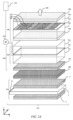
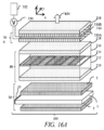
図1Aは、ディスプレイ装置の光学積層体を側面斜視図で示す概略図である。 FIG. 1A is a schematic diagram showing a side perspective view of an optical stack of a display device.
ディスプレイ装置100は、出力偏光子218である、少なくとも1つのディスプレイ偏光子を備える空間光変調器48を備える。バックライト20は光を出力するように構成されており、空間光変調器48は、バックライト20から出力光を受光するように構成されている、透過型空間光変調器48を備える。ディスプレイ装置100は、本明細書に記載するように、角度輝度特性を有する光400を出力するように構成されている。
本開示では、空間光変調器48は、基材212、216と、赤色、緑色、及び青色の画素220、222、224を有する液晶層214と、を備える液晶ディスプレイを備えてよい。空間光変調器48は、その両側に入力ディスプレイ偏光子210と出力ディスプレイ偏光子218とを有する。出力ディスプレイ偏光子218は、空間光変調器48の画素220、222、224からの光に対して高消光率をもたらすように構成されている。典型的な偏光子210、218は、ダイクロイック偏光子など吸収型偏光子であってよい。
In the present disclosure, spatial
任意に、反射型偏光子208がダイクロイック入力ディスプレイ偏光子210とバックライト210との間に設けられて、再循環光をもたらし、ディスプレイ効率を向上させ得る。有利なことには、効率を向上し得る。
Optionally, a
バックライト20は、入力光源15と、導波路1と、後方反射器3と、ディフューザ、光転向フィルム、及び他の既知の光バックライト構造体を備える光学積層体5と、を備えてよい。例えば非対称の表面レリーフ特徴部を備え得る非対称ディフューザが光学積層体5内に設けられ、横方向と比較して仰角方向の拡散が増大してよい。有利なことには、画像均一性が向上され得る。
The
本実施形態では、バックライト20は、以下の図26A~28Cに記載するように、正面輝度と比較して、軸外視聴位置に対して低下した輝度を有する角度光分布をもたらすように構成されてよい。バックライト20は、プライバシー動作モードでは低下した軸外輝度、広角動作モードでは増加した軸外輝度をもたらすために、出力角度輝度プロファイルを切り替えるように構成されている、切り替え可能なバックライトを更に備えてよい。かかるスイッチングバックライト20は、本実施形態の切り替え可能な補償リターダ300と協働し得る。
In this embodiment, the
追加偏光子318は、吸収型ダイクロイック偏光子であり得るディスプレイ出力偏光子218と同じ空間光変調器48の出力側に配置される。
An
ディスプレイ偏光子218及び追加偏光子318は、平行である電気ベクトル伝達方向219、319を有する。以下に記載するように、かかる平行配向は、中央視聴位置に高透過率をもたらす。
The
本明細書で共に切り替え可能な補償リターダ300と称される複数のリターダは、追加偏光子318とディスプレイ偏光子218との間に配置され、(i)ディスプレイ偏光子218と追加偏光子318との間に配置された液晶材料の層314を備える、切り替え可能な液晶リターダ301と、(ii)受動補償リターダ330と、を備える。
A plurality of retarders, referred to herein as compensating
図1Bは、図1Aの光学積層体内の光学層の配向を正面図で示す概略図である。空間光変調器48の入力ディスプレイ偏光子210における入力電気ベクトル伝達方向211は、液晶層214によって変換され得る入力偏光成分を提供して、出力ディスプレイ偏光子218の電気ベクトル伝達方向219によって決定される出力偏光成分を提供する。受動補償リターダ330は、ディスコティック複屈折材料430を含む遅延層を備えてよく、切り替え可能な液晶リターダ301は、液晶材料を含んでよい。
FIG. 1B is a schematic diagram showing the orientation of the optical layers in the optical stack of FIG. 1A in front view. The input electric
切り替え可能な補償リターダ300は、したがって、切り替え可能な液晶リターダ301及び基材312、316を備える切り替え可能な液晶リターダ301と、追加偏光子318とディスプレイ偏光子218との間に配置された受動補償リターダ330と、を備える。
The
基材312、316は、ガラス基材又はポリイミド基材などポリマー基材であってよい。好都合に透明電極が設けられ得る可撓性基材が提供され得る。有利なことには、湾曲した、屈曲した、折り畳み可能なディスプレイが提供され得る。
The
ディスプレイ装置100は、切り替え可能な液晶リターダ301の電極全体に電圧ドライバ350によって印加される電圧を制御するように構成されている制御システム352を更に備える。
The
発光ディスプレイの迷光の低減又はプライバシー制御の提供が望ましい場合がある。 It may be desirable to reduce stray light or provide privacy control in emissive displays.
図1Cは、発光型空間光変調器48と、発光型空間光変調器48の出力側に配置された切り替え可能な補償リターダ300と、を備える指向性ディスプレイ装置の光学積層体を側面斜視図で示す概略図である。
FIG. 1C shows in side perspective view the optical stack of a directional display device comprising an emissive spatial
あるいは、空間光変調器48は、有機LEDディスプレイ(OLED)など発光によって出力光400をもたらす他のディスプレイタイプによって提供され得、出力ディスプレイ偏光子218と、基材512、516と、発光層514と、を備える。出力偏光子218は、出力ディスプレイ偏光子218とOLED画素平面との間に挿入された1つ以上のリターダ518によってOLED画素平面から反射された光の輝度を低下させ得る。1つ以上のリターダ518は、1/4波長板であってよく、本開示の補償リターダ330とは異なる。
Alternatively, spatial
図1Cの実施形態では、空間光変調器48は、発光型空間光変調器を備え、ディスプレイ偏光子は出力ディスプレイ偏光子218である。
In the embodiment of FIG. 1C, spatial
そうでなければ、図1Cの指向性ディスプレイ装置は、上述のように、図1Aと同じである。 Otherwise, the directional display device of FIG. 1C is the same as that of FIG. 1A, as described above.
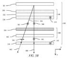
ここで、ディスプレイ装置に適用するための視野角制御光学素子260について説明する。視野角制御光学素子260は、切り替え可能な視野特性を達成するために、ディスプレイ偏光子210、218を備える空間光変調器に加えられてよい。
Here, the viewing angle control
図1Dは、受動補償リターダ330と、切り替え可能な液晶リターダ301と、制御偏光子250と、を備えるディスプレイ装置に適用するための視野角制御光学素子260を側面斜視図で示す概略図である。
FIG. 1D is a schematic diagram showing in side perspective view a viewing angle control
使用する際、視野角制御光学素子260は、偏光出力空間光変調器48にユーザによって、又は工場で取り付けられてよい。視野角制御光学素子260は、湾曲したディスプレイ及び屈曲したディスプレイのための可撓性フィルムとして提供されてよい。あるいは、視野角制御光学素子260は、ガラス基材など剛性基材上に設けられてよい。
In use, the viewing
有利なことには、パネルの画素分解能に一致させてモアレアーチファクトを回避する必要がない、アフターマーケットのプライバシー制御素子及び/又は迷光制御素子が提供され得る。視野角制御光学素子260は、空間光変調器48に工場で取り付けるように更に提供され得る。
Advantageously, aftermarket privacy and/or stray light control elements can be provided that do not need to match the pixel resolution of the panel to avoid moiré artifacts. A viewing
図1Dの視野角制御光学素子260を既存のディスプレイ装置に取り付けることにより、図1A~図1Cのいずれかに示されるようなディスプレイ装置を形成することができる。
By attaching the viewing
図1A~図1Dの実施形態は、空間光変調器48から出力される光400の極性輝度を制御する。すなわち、切り替え可能な補償リターダ300(切り替え可能な液晶リターダ301と、受動補償リターダ330と、を備える)は、切り替え可能な補償リターダ300の平面の法線に沿った軸に沿って入力ディスプレイ偏光子210、切り替え可能な補償リターダ300、及び追加偏光子318を通過する光の輝度に影響を及ぼさないが、切り替え可能な補償リターダ300は、切り替え可能な補償リターダ300の切り替え可能な状態のうちの少なくとも1つにおいて、切り替え可能な補償リターダ300の平面の法線に対して傾斜した軸に沿って通過する光の輝度を低下させる。この効果をもたらす原理は、図29A~図31Eを参照して以下でより詳細に説明しており、切り替え可能な液晶リターダ301及び受動補償リターダ330によって導入される、切り替え可能な液晶リターダ301及び受動補償リターダ330の液晶材料に関して異なる角度をなす軸に沿った光に対する位相シフトの有無から生じる。同様の効果が、以下に記載するすべての装置において達成される。
The embodiments of FIGS. 1A-1D control the polar intensity of
更に、切り替え可能な液晶リターダ301に加えて受動補償リターダ330を設けることにより、いくつかの特定のディスプレイ装置を参照し、図19A~図19Eを参照して記載するいくつかの比較例と比較することによってより詳細に説明するように、性能が改善される。
Further, by providing a passive compensating
空間光変調器48と観察者との間の光学層の数を低減することが望ましい場合がある。ここで、複数のリターダ300が空間光変調器48の入力側に配置される構成について説明する。
It may be desirable to reduce the number of optical layers between spatial
図2Aは、バックライト20と、切り替え可能な後方補償リターダ300と、透過型空間光変調器48と、を備える指向性ディスプレイ装置の光学積層体を側面斜視図で示す概略図であり、追加偏光子318は反射型偏光子を備える。図2Bは、図2Aの光学積層体内の光学層の配向を正面図で示す概略図である。
FIG. 2A is a schematic diagram showing in perspective side view the optical stack of a directional display device comprising a
ディスプレイ装置100は、空間光変調器48と、空間光変調器48の入力側に配置されたディスプレイ偏光子210と、を備える。追加偏光子318は、ディスプレイ偏光子210と同じ空間光変調器48の側に配置される。追加偏光子318は、バックライト20と協働して動作する反射型偏光子であって、効率を向上させる。
The
複数のリターダ300は、反射型追加偏光子318とディスプレイ偏光子210との間に配置される。図1Aのように、複数のリターダ300は、ディスプレイ偏光子210と反射型追加偏光子318との間に配置された液晶材料の層314を備える切り替え可能な液晶リターダ301と、受動補償リターダ330と、を備える。したがって、反射型追加偏光子318は、入力ディスプレイ偏光子210とバックライト20との間の入力ディスプレイ偏光子210の入力側に配置され、複数のリターダ300は、反射型追加偏光子318と入力ディスプレイ偏光子210との間に配置される。
A plurality of
反射型追加偏光子318の電気ベクトル伝達方向319は、以下に記載するように、入力偏光子210の電気ベクトル伝達方向211に対して平行であって、切り替え可能な方向特性を達成する。
The electric
代替的な実施形態では、追加偏光子318は、反射型偏光子及び吸収型ダイクロイック偏光子の両方を備えてよい、又はダイクロイック偏光子のみを備えてよい。
In alternative embodiments,
反射型追加偏光子318は、例えば、3M Corporation製のDBEF(商標)など多層フィルムであってよい、又はワイヤーグリッド偏光子であってよい。有利なことには、偏光子372からの偏光反射からの光を再利用することにより、ディスプレイ効率が改善され得る。吸収型ダイクロイック偏光子及び反射型偏光子の両方を追加偏光子318として使用する場合と比較すると、コスト及び厚さが更に低減され得る。
Reflective
図1Aの構成と比較して、図2Aは、画素220、222、224と観察者との間の層の数が低減しているため、スクリーン画像コントラストの前面が改善され得る。
Compared to the configuration of FIG. 1A, FIG. 2A has a reduced number of layers between the
図2Cは、バックライト20と、切り替え可能な後方補償リターダ300と、透過型空間光変調器48と、を備える指向性ディスプレイ装置の光学積層体を側面斜視図で示す概略図であり、追加偏光子318はダイクロイック偏光子を備える。図2Aの反射型追加偏光子318と比較して、ダイクロイック追加偏光子318は、高角度光をバックライトに再利用しないため、図2Aの構成と比較して軸外輝度を低下させ得る。有利なことには、プライバシー性能が改善される。
FIG. 2C is a schematic diagram showing in side perspective view the optical stack of a directional display device comprising a
ここで、図1A~図1C及び図2A~図2Bの切り替え可能な補償リターダ300及び追加偏光子318の構成及び動作について説明する。
The construction and operation of switchable compensating
図3は、負の誘電異方性を有する液晶材料414の層314を備える切り替え可能な液晶リターダ301の例示的な構成を側面図で示す概略図である。基材312、316は、その上に配置された透明電極413、415と、切り替え可能な液晶リターダ301の両側に配置されたホメオトロピック表面配向層409、411と、を有してよい。ホメオトロピック配向層409、411は、隣接する液晶材料414において、プレチルト角407を有するホメオトロピック配向をもたらし得る。
FIG. 3 is a schematic diagram illustrating in side view an exemplary configuration of a switchable
x-y面における液晶材料414の配向は、各配向層がプレチルトを有するように、配向層のプレチルト方向によって決定され、各配向層のプレチルトは、出力ディスプレイ偏光子218の電気ベクトル伝達方向303に対して平行若しくは逆平行である、又は直交している切り替え可能な液晶リターダ301の平面内に成分417a、417bを有するプレチルト方向を有する。
The orientation of the
プレチルト407a、407bは、例えば、88度であってよく、その結果、成分417が小さく、液晶材料414の層314の配向の緩和(ゼロ電圧)状態でディスクリネーションを低減する。したがって、層314は、ゼロ電圧構成の実質的に正のCプレートによって設けられる。実際には、液晶層は、角度407a及び残差成分417におけるホメオトロピック配向層のプレチルトによって提供される、わずかなOプレート特性を更に有する。
The pretilts 407a, 407b may be, for example, 88 degrees, so that the
切り替え可能な液晶リターダ301は、切り替え可能な液晶リターダ301に隣接して、切り替え可能な液晶リターダ301の両側に配置された電極413、415を備える。液晶材料414の層314は、電極413、415の全体に印加される電圧によって切り替え可能である。
The switchable
非駆動状態では、液晶材料414は、リターダ301の平面に対して垂直である成分418及びリターダの平面内の成分417と整列される。
In the undriven state, the
リターダ330は、ディスコティック複屈折材料430を含む負の受動Oプレートを備えるものとして図示されている。受動補償リターダ330のリターダンスは、切り替え可能な液晶リターダ301のリターダンスと等しく、かつ反対であり得る。切り替え可能な液晶リターダ301は、第1のプレチルト407aと、第2のプレチルト407bと、を備えてよく、受動補償リターダ330は、第1のプレチルト405a及び第2のプレチルト405bを有する補償リターダを備えてよく、補償リターダ330の第1のプレチルト405aは、液晶リターダ301の第1のプレチルト407aと同一であり、補償リターダ330の第2のプレチルト405bは、液晶リターダ301の第2のプレチルト307bと同一である。
受動Oプレートは、例えば、ディスコティック反応性メソゲンであり得る硬化反応性メソゲン層を備えてよい。補償リターダのプレチルトは、好適な配向層との整列後に反応性メソゲン材料を硬化させることによって達成され得る。Oプレートはまた、ポリカーボネートなどの二重延伸ポリマーフィルムを備えてよい。 A passive O-plate may comprise a hardened reactive mesogenic layer, which may be, for example, a discotic reactive mesogen. Pre-tilt of the compensating retarder can be achieved by curing the reactive mesogenic material after alignment with a suitable alignment layer. The O-plate may also comprise a double oriented polymer film such as polycarbonate.
動作中、切り替え可能な液晶リターダ301は、2つの配向状態間で切り替え可能である。第1の状態は、複数の視聴者によるディスプレイの視聴をもたらし得る。第2の状態は、プライバシー動作のための狭角モード、又は、例えば夜間動作における迷光の低減をもたらし得る。以下で更に説明するように、かかる素子は、広角動作モードでの広範囲の極角、及びプライバシー動作モードでの制限された輝度極性視野のために高透過率を提供することができる。
In operation, the switchable
ここで、第1の状態を表す、広角モードの図1Aのディスプレイの動作について説明する。 Operation of the display of FIG. 1A in wide-angle mode, representing the first state, will now be described.
図4Aは、広角動作モードの、切り替え可能な補償リターダ300の構成を斜視側面図で示す概略図である。切り替え可能な液晶リターダ301の全体にゼロボルトが提供される。図4A及び以下の他の概略図では、明確にするために光学積層体の一部の層を省略する。例えば、切り替え可能な液晶リターダ301は、基材312、316を省略して示されている。
FIG. 4A is a schematic diagram showing, in perspective side view, a
切り替え可能な液晶リターダ301は、液晶材料414の両側でそれに隣接し、隣接する液晶材料414においてホメオトロピック配向をもたらすように構成されている2つの表面配向層を備える。上記のように、液晶材料414には、例えば、水平から88度のプレチルトが設けられて、液晶材料414の配向の縮退を除去してよい。
The switchable
受動補償リターダ330は、リターダの平面に対して垂直な高速軸である光軸を有する、負のCプレートリターダを備える。したがって、Cプレートリターダの材料430は、負の誘電異方性を有し得る。Cプレートは、例えば、ホメオトロピック配向をもたらす、基材上に流延されるポリカーボネート又は反応性メソゲン、Zeonex(商標)シクロオレフィンポリマー(COP)、ディスコティックポリマー、及びNitto Denko(商標)二重延伸ポリカーボネートなど透明複屈折材料を含んでよい。
図4Bは、切り替え可能な液晶リターダセルを通る分数位置440に対する液晶ダイレクタ角度407のグラフを示す概略図であり、分数位置440は、表面配向層409における位置0と、表面配向層411における位置1の間で変動する。
FIG. 4B is a schematic diagram showing a graph of liquid
図4Aに示すように電圧が印加されていない垂直配向モードでは、液晶ダイレクタは、チルトプロファイル442によって示されるように、セルの厚さを通して88度のチルト407である。層314のチルトプロファイルは、プロファイル442と同一であり得る。補償リターダ330は、切り替え可能な液晶リターダ301のプレチルト方向を補正してよい。あるいは、補償リターダ330は、90度の均一チルト角を有してよく、液晶層のプレチルトのかかる差は、軸外視聴特性にごくわずかな差をもたらす。
In vertical alignment mode with no voltage applied as shown in FIG. 4A, the liquid crystal director is tilted 407 by 88 degrees through the thickness of the cell as shown by
したがって、補償リターダ330の軸外リターダンスは、電圧が印加されていないとき、切り替え可能な液晶リターダ301の軸外リターダンスと実質的に等しく、かつ反対である。
Thus, the off-axis retardance of compensating
図4Cは、広角動作モードでの、図1Aの光学積層体を通る、空間光変調器48からの出力光の伝搬を側面図で示す概略図であり、図4Dは、広角動作モードでの、図4Cの透過光線の極性方向での出力透過の変化を示す概略グラフである。
FIG. 4C is a schematic diagram illustrating in side view the propagation of output light from spatial
理想的な切り替え可能な補償リターダ300は、切り替え可能な可変液晶リターダ301と組み合わせて補償リターダ330を備え、補償リターダ330の誘電率、異方性、及び異方性の分散は、層314の誘電率、異方性、及び異方性の分散と等しく、かつ反対である誘電率、異方性、及び異方性の分散を有する。受動補償リターダ330のリターダンスは、切り替え可能な液晶リターダ301のリターダンスと等しく、かつ反対である。
An ideal
かかる理想的な補償切り替え可能なリターダは、すべての極角について液晶材料414の層314の第1の広角状態で透過光の補償を達成し、切り替え可能な液晶リターダ301の第2のプライバシー状態で横方向の狭視野を達成する。
Such an ideal compensating switchable retarder achieves compensation of transmitted light in the first wide-angle state of
更に、補償リターダ330の光軸は、広角状態の液晶リターダ301の光軸と同一方向を有する。かかる補償リターダ330は、すべての視野角について液晶リターダの遅延を相殺し、すべての視野方向について輝度損失のない、理想的な広角視野状態をもたらす。
Furthermore, the optical axis of compensating
ここで、理想的ではない材料選択の広角透過極性プロファイルについて説明する。 A wide-angle transmission polar profile for non-ideal material selection is now described.
本開示の例示的な実施形態は、リターダ330、301に典型的である材料特性の差が小さいために、切り替え可能な液晶リターダ301の遅延を厳密には補償できない補償リターダ330を示す。しかしながら、有利なことには、かかる偏差は小さく、かかる偏差が理想的な性能に近ければ、高性能の広角状態及び狭角状態が達成され得る。
Exemplary embodiments of the present disclosure
したがって、切り替え可能な液晶リターダ301が前述の2つの状態のうちの第1の状態であるとき、切り替え可能な補償リターダ300は、光線402などについて偏光成分360、361を全変換せず、切り替え可能なリターダの平面に対して垂直に、又は切り替え可能なリターダの平面に対して垂直と鋭角をなして通過する光線400を出力する。
Thus, when the switchable
偏光成分362は偏光成分360と実質的に同一であり、偏光成分364は偏光成分361と実質的に同一である。したがって、図4Dの角度透過プロファイルは、広範な極性領域にわたって実質的に均一に伝達される。
換言すれば、液晶材料414の層が上記2つの配向状態のうちの第1の配向状態にあるとき、複数のリターダ330、301は、リターダの平面に対して垂直に、又はリターダ330、301の平面に対して垂直と鋭角をなして通過する光に対して全体的なリターダンスを提供しない。
In other words, when the layer of
有利なことには、第1の状態の視野角を有するディスプレイ輝度の変化は、実質的に変更されない。複数のユーザは、好都合には、ディスプレイを広範な視野角から見ることができる。 Advantageously, the change in display brightness with the viewing angle of the first state is substantially unchanged. Multiple users can conveniently view the display from a wide range of viewing angles.
ここで、例えば、プライバシー動作モードで使用するための、狭角モードでの補償リターダ300及び追加偏光子318の動作について説明する。
Operation of compensating
図5Aは、プライバシー動作モードの負のCプレート受動補償リターダ330と、ホメオトロピック配向の切り替え可能な液晶リターダ301と、を備える、プライバシー動作モードの切り替え可能な補償リターダ300の構成を斜視側面図で示す概略図である。
FIG. 5A shows in perspective side view a configuration of a
液晶リターダ301は、切り替え可能な液晶リターダ301全体に配置されたITO電極など透明電極413、415を更に備える。電極413、415は、電極413、415に印加される電圧を調整することによって切り替え可能な液晶リターダ301を制御する。
The
制御システム352は、電圧ドライバ350によって切り替え可能な液晶リターダ301の電極413、415の全体に印加される電圧を制御するように構成されている。
図4Bに戻ると、電圧が印加されると、切り替え可能な液晶リターダ301の外広がりのチルトプロファイル444がもたらされ、その結果、液晶材料414の層314のリターダンスが変更される。
Returning to FIG. 4B, the application of a voltage results in the
最適なプライバシー性能の方向は、駆動電圧を制御することによって観察者の位置に応じて調整されてよい。別の使用では、又は、例えば自動車環境において軸外観察者に制御された輝度を提供するために、乗客又は運転者が、表示された画像を完全に不明瞭化するのではなく、中間電圧レベルを用いてある程度の視認性を提供することを望む場合がある。 The direction of optimal privacy performance may be adjusted according to the observer's position by controlling the drive voltage. In another use, or to provide controlled brightness to an off-axis observer, for example in a motor vehicle environment, a passenger or driver may use an intermediate voltage level rather than completely obscuring the displayed image. , to provide some visibility.
図5Bは、プライバシー動作モードでの、図1Aの光学積層体を通る空間光変調器48からの出力光の伝搬を側面図で示す概略図であり、切り替え可能な液晶リターダ301は、印加された電圧によって配向される。
FIG. 5B is a schematic diagram illustrating in side view the propagation of output light from spatial
本実施形態では、切り替え可能な補償液晶リターダ330は、ディスプレイ偏光子210、218、316及び追加偏光子318と組み合わせて、光軸(軸外)と鋭角をなすディスプレイ装置からの光出力の輝度が低下する(すなわち、リターダが存在しない場合と比較して)効果を有するように構成されてよい。切り替え可能な補償液晶リターダ330はまた、ディスプレイ偏光子210、218、316及び追加偏光子318と組み合わせて、光軸(軸上)に沿った、ディスプレイ装置からの光出力の輝度が低下しない(すなわち、リターダが存在しない場合と比較して)効果を有するように構成されてよい。
In this embodiment, the switchable compensating
出力ディスプレイ偏光子218からの偏光成分360は、出力ディスプレイ偏光子218によって透過され、切り替え可能な補償リターダ300に入射する。軸上光は、成分360からの未変更の偏光成分362を有し、軸外光は、切り替え可能な補償リターダ300のリターダによって変換される偏光成分364を有する。少なくとも、偏光成分361は、直線偏光成分364に変換され、追加偏光子318によって吸収される。より一般的には、偏光成分361は、楕円偏光成分に変換され、追加偏光子318によって部分的に吸収される。
したがって、リターダ切り替え可能な液晶リターダ301が当該2つの配向状態のうちの第2の配向状態にあるとき、複数のリターダ301、330は、リターダの平面に対して垂直である軸に沿って通過する光に対して全体的なリターダンスをもたらさないが、リターダ301、330の平面に対して垂直と鋭角をなす一部の極角363には、通過する光に対してゼロでない全体的なリターダンスをもたらす。
Thus, when the retarder-switchable
換言すれば、切り替え可能な液晶リターダ301が当該2つの状態のうちの第2の状態にあるとき、切り替え可能な補償リターダ330は、切り替え可能なリターダ301の平面に対して垂直である軸に沿って通過する出力光線400に対して偏光成分360を全変換しないが、リターダ301、330の平面に対して垂直と鋭角をなす一部の極角については、通過する光線402に対して偏光成分361を全変換する。
In other words, when the switchable
例示的な材料システムは、狭角動作について説明する。 The exemplary material system describes narrow angle operation.
図5Cは、図5Bの透過光線の極性方向での出力透過の変化を示す概略グラフであり、表1に記載のパラメータを有する。

本実施形態では、遅延及び電圧の望ましい範囲は、リターダ積層体のシミュレーション及びディスプレイ光学積層体を用いた実験によって確立されている。 In this embodiment, the desired ranges of delay and voltage are established through retarder stack simulations and experiments with display optics stacks.
切り替え可能な液晶リターダ300は、液晶材料414の層の第1の側に配置された第1表面配向層409と、第1の側と反対側の液晶材料414の層の第2の側に配置された第2の表面配向層411と、を備え、第1の表面配向層409はホメオトロピック配向層であり、第2の表面配向層411は、ホメオトロピック配向層であり、液晶材料の層は、550nmの波長の光に対して500nm~1000nm、好ましくは600nm~900nm、最も好ましくは700nm~850nmのリターダンスを有する。
The switchable
受動補償リターダ330が、リターダの平面に対して垂直である光軸を有するリターダを備える場合、受動リターダは、550nmの波長の光に対して-300nm~-900nm、好ましくは-450nm~-800nm、最も好ましくは-500nm~-725nmのリターダンスを有する。
If the
図5Cに示す光透過の極性分布は、下方に位置する空間光変調器48からの輝度出力の極性分布を変更し、該当する場合にはバックライト20についても変更する。
The polar distribution of light transmission shown in FIG. 5C modifies the polar distribution of the luminance output from the underlying spatial
有利なことには、軸上の観察者に対して高輝度を維持しつつも、軸外のスヌーパーに対して低輝度を有するプライバシーディスプレイが提供される。軸外のスヌーパーに対するディスプレイの輝度が低下する、広範な極性領域が提供される。更に、プライバシー動作モードの主たるディスプレイユーザは、軸上輝度の影響を実質的に受けない。 Advantageously, a privacy display is provided that has low brightness for off-axis snoopers while maintaining high brightness for on-axis observers. A wide polar region is provided in which the brightness of the display is reduced for off-axis snoopers. Furthermore, the primary display user in privacy mode of operation is substantially unaffected by on-axis luminance.
電極全体に印加される電圧は、第1の配向状態ではゼロであり、第2の配向状態ではゼロではない。有利なことには、広角動作モードでは追加の電力消費は生じなくてよく、切り替え可能な液晶リターダ301の駆動の故障モードは広角モード用である。
The voltage applied across the electrodes is zero in the first orientation and non-zero in the second orientation. Advantageously, no additional power consumption may occur in the wide-angle mode of operation, and the failure mode of driving the switchable
ここで、図1Aのディスプレイのプライバシーモードの動作について更に説明する。 The privacy mode operation of the display of FIG. 1A will now be further described.
図6Aは、プライバシーモードで動作するディスプレイについての透過出力光の観測を正面斜視図で示す概略図である。ディスプレイ装置100は、白色領域603と、黒色領域601と、を備えてよい。スヌーパーは、観察領域601、603間の輝度差が知覚され得る場合、ディスプレイ上の画像を観察することができる。動作中、主たるユーザ45は、指向性ディスプレイの光学窓であり得る視聴位置26までの光線400によって全輝度画像を観察する。スヌーパー47は、指向性ディスプレイの光学窓であり得る視聴位置27において、低減された輝度光線402を観察する。領域26、27は、図5Cの軸上領域及び軸外領域を更に表す。
FIG. 6A is a schematic diagram showing in front perspective view the observation of transmitted output light for a display operating in privacy mode. The
図6Bは、プライバシーモード1で動作する図1Aのディスプレイの見え方を正面斜視図で示す概略図であり、輝度は、図5Cに示すように変化する。したがって、上視野象限530、532、下視野象限534、536、及び横視聴位置526、528は輝度の低下をもたらし、一方、上/下中央視聴領域522、520及び正面視聴は、より高い輝度をもたらす。
FIG. 6B is a schematic diagram showing, in front perspective view, the appearance of the display of FIG. 1A operating in
自動車車両において制御可能なディスプレイ照明を提供することが望ましい場合がある。 It may be desirable to provide controllable display lighting in automotive vehicles.
図6Cは、エンターテイメント動作モード及び共有動作モードの両方について、車両600の車室602内に配置された切り替え可能な指向性ディスプレイ100を有する自動車車両を側面図で示す概略図である。光円錐610(例えば、輝度がピーク輝度の50%を超える光の円錐を表す)は、ディスプレイ100の仰角方向の輝度分布によって提供されてよく、切り替え不能である。
FIG. 6C is a schematic diagram showing in side view a motor vehicle having a switchable
図6Dは、エンターテイメント動作モードであって、プライバシーディスプレイと同様に動作する、車室602内に配置された切り替え可能な指向性ディスプレイ100を有する自動車車両を正面図で示す概略図である。光円錐612は、乗客606がディスプレイ100を見ることができるが、運転手604はディスプレイ100上の画像を見ることができないように、狭角度範囲で提供される。有利なことには、エンターテイメント画像は、運転手604の注意を乱すことなく、乗客606に表示され得る。
FIG. 6D is a schematic diagram showing a front view of an automotive vehicle in an entertainment mode of operation and having a switchable
図6Eは、共有動作モードの、車室602内に配置された切り替え可能な指向性ディスプレイ100を有する自動車車両を上面図で示す概略図である。光円錐614は、例えば、ディスプレイが動いていないとき、又は注意を乱さない画像が提供されるときに、全乗員がディスプレイ100上の画像を知覚することができるように、広角度範囲で提供される。
FIG. 6E is a schematic diagram showing in top view an automotive vehicle having a switchable
図6Fは、夜間動作モード及び日中動作モードの両方について、車室602内に配置された切り替え可能な指向性ディスプレイ100を有する自動車車両を上面図で示す概略図である。図6C~図6Eの構成と比較して、光学出力は、ディスプレイの仰角方向が運転手604と乗客606の位置との間の軸に沿うように回転される。光円錐620は、運転手604及び乗客606の両方を照らす。
FIG. 6F is a schematic diagram showing, in top view, an automotive vehicle having a switchable
図6Gは、夜間動作モードの、車室602内に配置された、切り替え可能な指向性ディスプレイ100を有する自動車車両を側面図で示す概略図である。したがって、ディスプレイは、狭角度の出力光円錐622を提供し得る。車室602の内側面及び乗客を照らし、有利なことには、運転手604の注意を乱す迷光は、実質的に低減され得る。運転手604及び乗客606の両方は、有利なことには、表示された画像を観察することができる。
FIG. 6G is a schematic diagram showing in side view a motor vehicle having a switchable
図6Hは、日中動作モードの、車室602内に配置された切り替え可能な指向性ディスプレイ100を有する自動車車両を側面図で示す概略図である。したがって、ディスプレイは、狭角度の出力光円錐624を提供し得る。有利なことには、ディスプレイは、車室602の全乗員によって好都合に観察され得る。
FIG. 6H is a schematic diagram showing in side view an automotive vehicle having a switchable
図6C~図6Hのディスプレイ100は、運転手機器用ディスプレイ、中央コンソールディスプレイ、及びシートバックディスプレイなど他の車室位置に配置され得る。
The
図7A~図7Dは、0.1V刻みで2.05V~2.35Vの4つの異なる駆動電圧に対する極性方向での出力透過の変化を示す概略図である。したがって、印加された電圧は、プライバシー動作モードにおける輝度視野最小位置を制御し得る。更に、輝度最小値は、極性プロファイルの上象限内の仰角に対してゼロ以下の仰角間で制御され得る。 7A-7D are schematic diagrams showing the variation of output transmission in the polar direction for four different drive voltages from 2.05V to 2.35V in 0.1V steps. The applied voltage can thus control the luminance field minimum position in the privacy mode of operation. In addition, the luminance minimum can be controlled between elevation angles below zero for elevation angles in the upper quadrant of the polar profile.
図8は、制御システムによって実行されるプライバシーディスプレイの制御を示すフローチャートである。この制御は、本明細書に記載する装置のそれぞれに適用されてよい。 FIG. 8 is a flow chart illustrating privacy display control performed by the control system. This control may be applied to each of the devices described herein.
第1の工程870では、ユーザは、プライバシー動作モードを有効にし得る。
In a
第1の、及び更なる補償切り替え可能な液晶リターダ300Bが設けられる場合(例えば、以下で説明する図22Aの装置において)、制御システムは第2の配向状態で配置されて、前述の切り替え可能な液晶リターダ314Aの電極413、415全体に印加される電圧を制御し、また、更なる切り替え可能な液晶リターダ314Bの電極全体に印加される電圧を制御し、リターダ31A、330Aの平面に対して垂直と鋭角をなす一部の極角で前述の第1の切り替え可能な液晶リターダ314A及び前述の受動補償リターダ330Aを通過する光に対する全体的なリターダンスは、一部の極角で更なる切り替え可能な液晶リターダ314B及び更なる受動補償リターダ330Bを通過する光に対する全体的なリターダンスとは異なる。
When first and further compensating switchable
かかるプライバシーモード設定は、手動設定(例えば、キーボード操作)によって、又は例えば、参照によりその全体が本明細書に組み込まれる米国特許出願公開第2017-0236494号に記載されているように、スヌーパーの存在を特定するセンサを使用した自動検知によって提供されてよい。任意に、スヌーパーに関するディスプレイの配向は、検出器873によって更に検出されてよい。
Such privacy mode settings can be set by manual setting (eg, keyboard operation) or by the presence of snoopers, for example, as described in US Patent Application Publication No. 2017-0236494, which is incorporated herein by reference in its entirety. may be provided by automatic detection using a sensor that identifies the Optionally, the orientation of the display with respect to the snooper may also be detected by
第2の工程872では、スヌーパーの位置は、例えばカメラ若しくはキーボード設定又は他の方法によって検出されてよい。例示的な実施例では、オフィス設定が提供されてもよく、このオフィス設定は、共有オフィス環境を動き回るスヌーパーに対するプライバシー性能を最適化することが望ましい場合があり、したがって下方視野象限に対して性能を最適化する。フライト設定と比較して、着席しているスヌーパーにプライバシーレベルの最適化をもたらし、オフィス設定に望ましい仰角よりも小さい仰角に対してプライバシーレベルを改善し得る。
In a
第3の工程876では、切り替え可能な液晶リターダ301に印加される電圧を調整してよく、第4の工程878では、制御システムでLEDプロファイルを調整することができる。
In a
したがって、制御システムは、ディスプレイ装置100に関してスヌーパー47の位置を判定する手段872を更に備えてよく、制御システムは、測定したスヌーパー47の位置に応答して、ドライブ350によって切り替え可能な液晶リターダ314の電極413、415全体に印加される電圧を調整するように構成されている。
Accordingly, the control system may further comprise means 872 for determining the position of the
有利なことには、ディスプレイのプライバシー動作は、スヌーパーのビューイングジオメトリ(viewing geometry)を最適化するように制御され得る。 Advantageously, the privacy behavior of the display can be controlled to optimize the viewing geometry of the snooper.
本実施形態の考察に戻り、切り替え可能な補償リターダ300の更なる構成について説明する。
Returning to the discussion of this embodiment, further configurations of the
図9Aは、交差Aプレート受動補償リターダ308A、308Bと、ホメオトロピック配向の切り替え可能な液晶リターダ301と、を備える、プライバシー動作モードの切り替え可能な補償リターダの構成を斜視側面図で示す概略図であり、図9Bは、交差Aプレート受動補償リターダと、ホメオトロピック配向の切り替え可能な液晶リターダと、を備える、プライバシー動作モードの切り替え可能な補償リターダの構成を斜視側面図で示す概略図である。
FIG. 9A is a schematic diagram showing in perspective side view a switchable compensating retarder configuration for privacy operation mode comprising crossed A-plate
図4A及び図5Aの構成と比較して、補償リターダ330は、代替的に、交差するリターダの平面に光軸を有する一対のリターダ308A、308Bを備えてよい。補償リターダ330は、したがって、それぞれ単一のAプレートを備える一対のリターダ308A、308Bを備える。
4A and 5A, compensating
一対のリターダ308A、308Bは、それぞれ、互いに関して異なる角度で配向されたそれぞれの光軸309A、309Bを有する複数のAプレートを備える。一対のリターダは、追加偏光子318が入力ディスプレイ偏光子の入力側に配置されている場合には入力ディスプレイ偏光子210の電気ベクトル伝達方向211に対して平行であり、追加偏光子318が入力ディスプレイ偏光子218の出力側に配置されている場合には出力ディスプレイ偏光子218の電気ベクトル伝達方向219に対して平行である、電気ベクトル伝達方向に関して45°でそれぞれ延在する、光軸309A、309Bを有する。
A pair of
図9Cは、広角動作モードでの、図9Aの透過光線の極性方向での出力透過の変化を示す概略グラフであり、図9Dは、プライバシー動作モードでの、図9Bの透過光線の極性方向での出力透過の変化を示す概略グラフであり、表2の例示的な実施形態によって提供される。

受動補償リターダ330が、交差するリターダの平面内に光軸を有する一対のリターダを備える場合、この一対のリターダの各リターダは、550nmの波長の光に対して300nm~800nmの範囲、好ましくは500nm~700nmの範囲、最も好ましくは550nm~675nmの範囲のリターダンスを有する。
If the
有利なことに、Aプレートは、好都合には、図4A及び図5AのCプレートリターダよりも低コストで製造され得る。広角動作モード用に、ゼロ電圧状態が更に提供され、広角動作中の電力消費を最小限に抑え得る。 Advantageously, A-plates can be conveniently manufactured at a lower cost than the C-plate retarders of FIGS. 4A and 5A. A zero voltage state may also be provided for the wide-angle mode of operation to minimize power consumption during wide-angle operation.
本実施形態において、「交差する」は、リターダの平面内の2つのリターダの光軸間の実質的に90°の角度を指す。リターダ材料のコストを低減するために、例えば、フィルム製造中の延伸誤差に起因して、リターダ配向に多少の変化を有する材料を提供することが望ましい。好ましい方向から離れるリターダ配向の変化は、正面輝度を低下させ、最小透過率を増加させ得る。好ましくは、角度310Aは、少なくとも35°かつ最大55°、より好ましくは少なくとも40°かつ最大50°、最も好ましくは少なくとも42.5°かつ最大47.5°である。好ましくは、角度310Bは、少なくとも125°かつ最大145°、より好ましくは少なくとも130°かつ最大135°、最も好ましくは少なくとも132.5°かつ最大137.5°である。
In this embodiment, "crossed" refers to an angle of substantially 90° between the optical axes of two retarders in the plane of the retarders. To reduce the cost of retarder materials, it is desirable to provide materials that have some variation in retarder orientation, for example due to stretching errors during film manufacture. A change in retarder orientation away from the preferred direction can reduce head-on brightness and increase minimum transmission. Preferably,
ディスプレイにタッチしているときなど機械的に歪んでいるとき、図9A~9Bのホメオトロピック配向の液晶リターダ301は、目に見えるミスアライメントアーチファクトを生じさせる、不必要に長い回復時間を有し得る。機械的な歪みの後に高速で回復することが望ましい。
When mechanically distorted, such as when the display is being touched, the homeotropically aligned
図10A~図10Bは、第1の駆動電圧及び第2の駆動電圧に対してCプレートリターダ330がそれぞれ正の誘電異方性及び受動の負のCプレートである液晶材料414を含み、ホモジニアス配向の切り替え可能な液晶リターダを備える、広角動作モード及びプライバシー動作モードでの切り替え可能な補償リターダの構成をそれぞれ斜視側面図で示す概略図である。
10A-10B show that the C-
切り替え可能な液晶リターダは、液晶材料414の層に隣接し、隣接する液晶材料内にホモジニアス配向をもたらすようにそれぞれ構成されている表面配向層431、433を更に含む。換言すると、切り替え可能な液晶リターダは、液晶材料414の層に隣接し、かつその両側に配置され、隣接する液晶材料414内にホモジニアス配向をもたらすようにそれぞれ構成されている、2つの表面配向層431、433を備える。
The switchable liquid crystal retarder further includes surface alignment layers 431, 433 adjacent the layer of
図10Cは、様々な異なる印加電圧についての図10Aの切り替え可能な液晶リターダ301を通る分数位置440に対する液晶ダイレクタ角度407のグラフを示す概略図である。図10Cは、プレチルト角が小さく、印加電圧と共に増加する図4Bとは異なる。プロファイル441は、0Vの印加電圧に対する液晶材料414のチルト角を示し、傾斜プロファイル443は、2.5Vに対するダイレクタ配向を示し、チルトプロファイル445は5Vに対するダイレクタ配向を示す。したがって、液晶層は、典型的には、望ましい切り替え状態で斜めであり、補償リターダ330によって補償される。2.5V超から10Vに電圧を増加させると、斜面が存在するリターダ301の厚さを漸進的に低減し、有利なことには、透過が最大になる極性視野を増大させる。
FIG. 10C is a schematic diagram showing a graph of liquid
リターダの平面に対して垂直である方向と比較した液晶チルトの分解成分419a、419bは、図5Aの成分417a、417bよりも実質的に高い。
The
分解成分419a、419bの増加した大きさは、例えば、図9Aの構成と比較して、機械的な歪みの後に増加した復元力をもたらし得る。ディスプレイにタッチする際などの機械的な歪みに対する感度は、有利なことに低減され得る。
The increased magnitude of the
動作の電圧は、許容可能な広角視野のために10V未満に低減され、電力消費を低減し、電気駆動のコスト及び複雑性を低減し得る。 The voltage of operation can be reduced to less than 10V for an acceptable wide-angle field of view, reducing power consumption and reducing the cost and complexity of electric driving.
図11A~図11Cは、プライバシーモード及び異なる駆動電圧に対する2つの異なる広角モードでの、図10A及び図10Bのディスプレイ装置と同様にホモジニアス配向の液晶リターダ301及び負の受動Cプレート補償リターダ330を備える切り替え可能な補償リターダの透過光線の極性方向での出力透過の変化を示す概略グラフであり、表3に示す実施形態を含む。

両基材上にホモジニアス配向層431、433を備える能動LCリターダ301の光学リターダンスの望ましい範囲、及び負の受動Cプレート補償リターダ330は、表4に更に記載する。

したがって、切り替え可能な液晶リターダ300は、液晶材料414の層の第1の側に配置された第1の表面配向層431と、第1の側と反対側の液晶材料414の層の第2の側に配置された第2の表面配向層433と、を備え、第1の表面配向層409はホモジニアス配向層であり、第2の表面配向層はホモジニアス配向層であり、液晶材料の層は、550nmの波長の光に対して500nm~1000nmの範囲、好ましくは600nm~850nmの範囲、最も好ましくは700nm~800nmの範囲のリターダンスを有する。したがって、第1の配向層及び第2の配向層はそれぞれホモジニアス配向層であり、受動補償リターダ330がリターダの平面に対して垂直である光軸を有するリターダを備えるとき、受動リターダは、550nmの波長の光に対して、-300nm~-700nmの範囲、好ましくは-350nm~-600nmの範囲、最も好ましくは-400nm~-500nmの範囲のリターダンスを有する。
Thus, the switchable
有利なことには、軸外プライバシーは、広い極性領域全体での輝度低下及びプライバシーレベルの増加によってもたらされ得る。層314内の液晶材料の流動から生じる視覚的アーチファクトに対する更なる抵抗は、ホメオトロピック配向と比較して改善され得る。
Advantageously, off-axis privacy can be provided by reduced brightness and increased privacy levels across a wide polar region. Further resistance to visual artifacts resulting from liquid crystal material flow within
ここで、図10Aの光学構造体の様々な他の構成及び駆動について説明する。 Various other configurations and actuation of the optical structure of FIG. 10A will now be described.
5Vでの動作は、広角モードで許容可能な輝度のロールオフを達成しつつ、より低い電力消費及び低コストの電子機器をもたらす。広角モードの視野は、10Vでの動作によって更に拡大され得る。 Operation at 5V results in lower power consumption and lower cost electronics while achieving acceptable luminance roll-off in wide-angle mode. The wide-angle mode field of view can be further enhanced by operation at 10V.
図12Aは、プライバシー動作モードの切り替え可能な補償リターダの構成を斜視側面図で示す概略図であり、この構成は、交差Aプレート受動補償リターダ308A、308Bと、ホモジニアス配向の切り替え可能な液晶リターダ301と、を備え、図12B~図12Dは、異なる駆動電圧についての、プライバシーモード及び広角モードでのホモジニアス配向の液晶材料414及び負の受動交差Aプレートリターダ308A、308Bを備える、切り替え可能な補償リターダ301の透過光線の極性方向での出力透過の変化を示す概略グラフであり、表5に示すそれぞれの実施形態を含む。

両基材上のホモジニアス配向層409、411と、正の能動交差Aプレート補償リターダ308A、308Bと、を備える能動LCリターダ301の光学リターダンスの望ましい範囲は、表6に更に記載する。

したがって、第1の配向層及び第2の配向層は、それぞれホモジニアス配向層であり、液晶材料の層は、550nmの波長の光に対して500nm~1000nmの範囲、好ましくは600nm~850nmの範囲、最も好ましくは700nm~800nmの範囲のリターダンスを有し、受動補償リターダ330は、交差するリターダの平面内に光軸を有する一対のリターダを備え、この一対のリターダの各リターダは、550nmの波長の光に対して300nm~800nm、好ましくは350nm~650nm、最も好ましくは450nm~550nmのリターダンスを有する。
Thus, the first alignment layer and the second alignment layer are each homogeneous alignment layers and the layer of liquid crystal material is in the
更なる交差Aプレートは、好都合には、低コスト材料から提供され得る。 Additional cross A-plates can be conveniently provided from low cost materials.
ここで、実例として、図12Aの光学構造及び駆動の様々な他の例示的な実施形態について説明する。図12C及び図12Dは、アドレス電圧及びリターダンスの調整によって、有利に異なる広角視野が達成され得ることを更に示す。 Various other exemplary embodiments of the optical structure and drive of FIG. 12A will now be described by way of illustration. Figures 12C and 12D further illustrate that by adjusting the address voltage and retardance, advantageously different wide-angle fields of view can be achieved.
ここで、光学積層構造体の構成について更に説明する。 Here, the configuration of the optical laminated structure will be further described.
図13A及び図13Bは、切り替え可能な補償リターダと、光学結合層380と、を備えるディスプレイの一部を側面図で示す概略図である。光学結合層380は、積層フィルム及び基材に設けられてよく、プライバシーモードの高視野角で効率を向上し、輝度を低下させる。更に、空間光変調器48と切り替え可能な補償リターダ300との間に空隙384が設けられてよい。空隙384における2つの表面の湿潤を低減するために、切り替え可能な補償リターダ300又は空間光変調器48のうちの少なくとも1つに、湿潤防止面382が設けられてよい。
13A and 13B are schematic diagrams showing in side view a portion of a display comprising a switchable compensating retarder and an
受動補償リターダ330は、図13Aに示すように切り替え可能な液晶層301と空間光変調器48との間に設けられてよい、又は図13Bに示すように、追加偏光子318と切り替え可能な液晶リターダ301との間に設けられてよい。両方のシステムにおいて、実質的に同一の光学性能が提供される。
A passive compensating
図13Aは、光学層が基材312、316の外側に結合されていることを示す。有利なことには、積層中に蓄積された応力により、取り付けられた層からの基材312、316の曲がりが低減し、ディスプレイの平坦性が維持され得る。
FIG. 13A shows that the optical layers are bonded to the outside of the substrates 312,316. Advantageously, stress built up during lamination may reduce bowing of the
同様に、切り替え可能な補償リターダ300が配置され得、出力偏光子218はディスプレイ偏光子である。画素220、222、224における位相構造などから空間光変調器48によってもたらされ得る散乱は、切り替え可能な補償リターダ301が空間光変調器48の背後に配置される構成と比較して、出力輝度プロファイルを劣化させない。
Similarly, a
ディスプレイ偏光子の電気ベクトル伝達方向とは異なる電気ベクトル伝達方向を有する追加偏光子を設けることが望ましい場合がある。 It may be desirable to provide an additional polarizer with an electrical vector transmission direction different from that of the display polarizer.
図14は、上述のように交差Aプレート受動補償リターダ308A、308Bと、ホモジニアス配向の切り替え可能な液晶リターダ301と、を備えるが、受動回転リターダ460を更に備える、プライバシー動作モードの切り替え可能な補償リターダの構成を斜視側面図で示す概略図である。
FIG. 14 shows a switchable compensation for privacy operation mode comprising crossed A-plate
ディスプレイ偏光子218は、ねじれネマティックLCDディスプレイの場合に、例えば45度の角度317であり得る、電気ベクトル伝達方向219を備えてよい。追加偏光子318は、典型的に垂直偏光を透過する偏光サングラスを着用し得るユーザに垂直偏光をもたらすように配置されてよい。
The
受動回転リターダ460は、本実施形態の補償リターダ330とは異なり、その動作についてはここで説明する。
Passive
受動回転リターダ460は、複屈折材料462を含んでよく、半波長板であって、例えば550nmの波長で275nmのリターダンスを有してよい。
Passive
受動回転リターダ460は、追加偏光子318の電気ベクトル伝達方向319に対して22.5度であり得る角度466で傾斜している、高速軸配向464を有する。したがって受動回転リターダ460は、補償リターダ308Bに入射する光の偏光方向が方向319に対して平行となるように、出力偏光子218からの偏光を回転させる。
Passive
受動回転リターダ460は、ディスプレイ偏光子218からの偏光成分の角度を回転させることによって、軸上偏光状態を変更する。比較すると、補償リターダ308A、308Bは、共に軸上偏光状態を変更しない。
Passive
更に、受動回転リターダ460は、視野角と実質的に無関係であり得る偏光を回転させる。比較すると、補償リターダ308A、308Bは、視野角に出力輝度の実質的な変更をもたらす。
Additionally, passive
有利なことには、ディスプレイは、例えば、偏光サングラス着用時に視聴できるように、ディスプレイ偏光子の偏光方向219とは異なる出力偏光方向319を備えてよい。
Advantageously, the display may have an
代替的な実施形態では、別個のリターダ460は省略されてもよく、リターダ308Aのリターダンスと比較して、追加の半波長回転を提供するために、図11Aのリターダ308Bのリターダンスを増加させてよい。例示的な実施形態を継続するために、波長550nmにおけるリターダ308Bのリターダンスは、リターダ308Aのリターダンスよりも275nm大きくてよい。有利なことには、層の数、複雑性、及びコストが低減され得る。
In an alternative embodiment,
光学部品の厚さ及び総数を低減することが望ましい。 It is desirable to reduce the thickness and total number of optical components.
図15Aは、第1のCプレート受動補償リターダ330Aと第2のCプレート受動補償リターダ330Bとの間に配置され、ホモジニアス配向の切り替え可能な液晶リターダ301を備える、プライバシー動作モードの切り替え可能な補償リターダの構成を斜視側面図で示す概略図であり、更に表7に示す。

図15B及び図15Cは、それぞれ広角動作モード及びプライバシー動作モードでの、図15Aの光学積層体内の透過光線の極性方向での出力透過の変化を示す概略グラフである。 15B and 15C are schematic graphs showing the variation of output transmission with the polar direction of transmitted light rays in the optical stack of FIG. 15A for wide-angle and privacy modes of operation, respectively.
受動補償リターダ330は、第1のCプレート330Aと、第2のCプレート330Bと、を備え、切り替え可能な液晶層301は、第1のCプレート330Aと第2のCプレート330Bとの間に設けられる。
受動補償リターダ330A、330Bは、受動リターダの平面に対して垂直である光軸を有する2つの受動リターダを備え、切り替え可能な液晶リターダ301は、2つの受動リターダの間に設けられる。したがって、図1Aの第1の基材312及び第2の基材316は、2つの受動リターダ330A、330Bのうちの1つをそれぞれ含む。
組み合わせると、2つの受動リターダ330A、330Bは、550nmの波長の光に対して-300nm~-800nmの範囲、好ましくは-350nm~-700nmの範囲、最も好ましくは-400nm~-600nmの範囲の総リターダンスを有する。
In combination, the two
図16Aは、それぞれCプレート受動補償リターダ330A、330Bを備える第1の基材と第2の基材との間に配置された、切り替え可能な液晶リターダ301を備えるディスプレイを斜視側面図で示す概略図であり、図16Bは、それぞれCプレート受動補償リターダ330A、330Bを備える第1の基材と第2の基材との間に配置された、切り替え可能な液晶リターダ301を備えるディスプレイの一部を側面図で示す概略図である。
FIG. 16A schematically shows in perspective side view a display comprising a switchable
第1のCプレート330Aは、片側に形成された透明電極層415と、液晶配向層411と、を有し、第2のCプレート330Bは、片側に形成された透明電極層413と、液晶配向層409と、を有する。
The first C-
液晶材料の層314は、第1の基材312と第2の基材316との間に設けられ、第1の基材312及び第2の基材316はそれぞれ、第1のCプレート330A及び第2のCプレー330Bのうちの1つを備える。Cプレートは、ITOコーティングされて、電極413、415を設け、その上に形成された液晶配向層409、411を有する、二重延伸COPフィルム内に設けられ得る。
A
有利なことには、層の数は、図1A、図1B、図1Cおよび図1Dの構成と比較して減少してよく、厚さ、コスト、及び複雑性も低下する。更に、Cプレート330A、330Bは可撓性基材であってよく、可撓性プライバシーディスプレイを提供し得る。
Advantageously, the number of layers may be reduced compared to the configurations of FIGS. 1A, 1B, 1C and 1D, reducing thickness, cost and complexity. Additionally, the C-
第1及び第2のAプレート基材間に液晶材料の層314を設けることが望ましい。
A
図17Aは、上述したように、第1の交差Aプレート受動補償リターダ330Aと第2の交差Aプレート受動補償リターダ330Bとの間に配置された、ホモジニアス配向の切り替え可能な液晶リターダ301を備える、広角動作モードの切り替え可能な補償リターダ300の構成を斜視側面図で示す概略図であり、図17B及び図17Cは、それぞれ広角動作モード及びプライバシー動作モードでの駆動時の、図17Aの構造の透過光線の極性方向での出力透過の変化を示す概略グラフであり、表7に示す更なる例示的な実施形態をそれぞれ含む。
FIG. 17A comprises a homogeneous orientation switchable
図15Aの構成と比較して、有利なことには、Aプレートは、Cプレートと比較して低減されたコストで製造され得る。 Advantageously, compared to the configuration of FIG. 15A, the A-plate can be manufactured at a reduced cost compared to the C-plate.
ここで、ホモジニアス配向層及びホメオトロピック配向層の両方を備えるハイブリッド配向構造について説明する。 Hybrid alignment structures comprising both homogeneous alignment layers and homeotropic alignment layers are now described.
図18Aは、液晶材料423を含むホモジニアス配向及びホメオトロピック配向の切り替え可能な液晶リターダ301と、負の受動Cプレートリターダ330と、を備える、プライバシー動作モードの切り替え可能な補償リターダの構成を斜視側面図で示す概略図である。
FIG. 18A shows a perspective side view of a configuration of a switchable compensating retarder for privacy operation mode, comprising a switchable
図18B~図18Cは、それぞれ広角動作モード及びプライバシー動作モードでの図18Aの透過光線の極性方向での出力透過の変化を示す概略グラフであり、表8の構成によって提供される。

ハイブリッド配向の切り替え可能な液晶リターダ301は、所与の材料及びセルの厚さの選択に対して有効複屈折が低減されるように可変チルトを有する。したがって、リターダ設計は、配向層が同一である構成と比較して補償するように調整される必要がある。切り替え可能な液晶リターダ330は、液晶材料423の層の第1の側に配置された第1表面配向層441と、第1の側と反対側の液晶材料423の層の第2の側に配置された第2の表面配向層443と、を備える。第1の表面配向層441は、隣接する液晶材料423内にホメオトロピック配向をもたらすように構成されているホメオトロピック配向層であり、第2の表面配向層443は、隣接する液晶材料423内にホモジニアス配向をもたらすように構成されているホモジニアス配向層である。
The hybrid orientation switchable
更に、リターダの最適な設計は、ホメオトロピック配向層及びホモジニアス配向層に関する受動補償リターダ330の相対位置に関連する。
Furthermore, the optimum retarder design is related to the relative position of the
表面配向層443が、液晶材料423の層と補償リターダ330との間にホモジニアス配向をもたらすように構成されている場合、液晶材料423の層は、550nmの波長の光に対して500nm~1800nmの範囲、好ましくは700nm~1500nmの範囲、最も好ましくは900nm~1350nmの範囲のリターダンスを有する。表面配向層443が、液晶材料423の層と補償リターダ330との間にホモジニアス配向をもたらすように構成されている場合、受動補償リターダは、図18Aに示すように、リターダの平面に対して垂直である光軸を有するリターダ330を備えてよく、受動リターダ330は、550nmの波長の光に対して-300nm~-1600nmの範囲、好ましくは-500nm~-1300nmの範囲、最も好ましくは-700nm~-1150nmの範囲のリターダンスを有する、あるいは、受動補償リターダは、交差するリターダの平面内に光軸を有する一対のリターダ(図示なし)を備えてよく、この一対のリターダの各リターダは、550nmの波長の光に対して400nm~1600nmの範囲、好ましくは600nm~1400nmの範囲、最も好ましくは800nm~1300nmの範囲のリターダンスを有する。
If the
表面配向層441が、液晶材料423の層と補償リターダ330との間にホメオトロピック配向をもたらすように構成されている場合、液晶材料423の層は、550nmの波長の光に対して700nm~2000nmの範囲、好ましくは1000nm~1700nmの範囲、最も好ましくは1200nm~1500nmの範囲のリターダンスを有する。表面配向層441が、液晶材料423の層と補償リターダ330との間にホメオトロピック配向をもたらすように構成されている場合、受動補償リターダは、図18Aに示すように、リターダの平面に対して垂直である光軸を有するリターダ330を備えてよく、受動リターダは、550nmの波長の光に対して-400nm~-1800nmの範囲、好ましくは-700nm~-1500nmの範囲、最も好ましくは-900nm~-1300nmの範囲のリターダンスを有する、あるいは、受動補償リターダは、交差するリターダの平面内に光軸を有する一対のリターダ(図示なし)を備えてよく、この一対のリターダの各リターダは、550nmの波長の光に対して400nm~1800nmの範囲、好ましくは700nm~1500nmの範囲、最も好ましくは900nm~1300nmの範囲のリターダンスを有する。
If the
図5Aの構成と比較して、プライバシー動作モードは、有利なことには、液晶リターダの押圧時に材料の流動の見え方に対する弾力性を増加させ得る。 Compared to the configuration of FIG. 5A, the privacy mode of operation can advantageously provide increased resilience to the appearance of material flow upon pressing of the liquid crystal retarder.
ここで、本実施形態との比較として、直列配置時の平行偏光子間のリターダの性能について説明する。まず、2つの異なる駆動電圧に対するホモジニアス配向の液晶リターダ301の視野について説明する。
Here, as a comparison with the present embodiment, retarder performance between parallel polarizers when arranged in series will be described. First, the field of view of the homogeneously aligned
図19Aは、ホモジニアス配向の切り替え可能な液晶リターダ390の構成を斜視側面図で示す概略図である。図19Bは、第1の印加電圧についての図19Aの透過光線の極性方向での出力透過の変化を示す概略グラフであり、図19Cは、第1の印加電圧よりも大きい第2の印加電圧についての図19Aの透過光線の極性方向での出力透過の変化を示す概略グラフであって、表9に示す構造を備える。ホモジニアス配向の切り替え可能な液晶リターダ390は、上述の切り替え可能な液晶リターダ330に対応し、本明細書に開示する装置のいずれかにおいて、切り替え可能な液晶リターダとして適用され得る。
FIG. 19A is a schematic diagram showing a configuration of a homogeneous alignment switchable
図19Dは、平行偏光子間に配置された受動Cプレートリターダ392を斜視側面図で示す概略図であり、図19Eは、図19Dの透過光線の極性方向での出力透過の変化を示す概略グラフであって、表9に示す構造を備える。受動Cプレートリターダ392は、受動補償リターダ330に対応し、本明細書に開示する装置のいずれかにおいて、少なくとも1つの受動補償リターダとして適用され得る。

図20Aは、平行偏光子396、398間に配置されたCプレートリターダ392を備える視野制御受動リターダと直列に、平行偏光子394、396間に配置された、ホモジニアス配向の切り替え可能な液晶リターダ390の構成を斜視側面図で示す概略図であり、図20Bは、第1の印加電圧についての図20Aの透過光線の極性方向での出力透過の変化を示す概略グラフであり、図20Cは、第1の印加電圧よりも大きい第2の印加電圧についての図20Aの透過光線の極性方向での出力透過の変化を示す概略グラフであって、表9に示す構造を備える。
FIG. 20A shows a homogeneous orientation switchable
図21Aは、Cプレート補償リターダ330と直列の、ホモジニアス配向の切り替え可能な液晶リターダ301の構成を斜視側面図で示す概略図であって、ホモジニアス配向の切り替え可能な液晶材料712及びCプレート補償リターダ330は、一対の平行偏光子間に配置されており、図21Bは、第1の印加電圧について図21Aの透過光線の極性方向での出力透過の変化を示す概略グラフであり、図21Cは、第1の印加電圧よりも大きい第2の印加電圧について図21Aの透過光線の極性方向での出力透過の変化を示す概略グラフであって、表9に示す構造を備える。
FIG. 21A is a schematic diagram showing in perspective side view a configuration of a homogeneously oriented switchable
予想外に、最大視野動作の最適条件は、その非駆動状態の切り替え可能な液晶リターダ301と比較して、補償リターダ330の等しく、かつ反対である正味遅延によって提供される。狭角状態をもたらすように構成されているとき、理想的な補償リターダ330及び切り替え可能な液晶リターダ301は、(i)入力光からの広角モード性能を変更せず、かつ(ii)すべての仰角の軸外位置に対して横方向視野角を最適に低減することができる。この教示は、本明細書に開示するすべてのディスプレイ装置に適用され得る。
Unexpectedly, the optimum for maximum field of view operation is provided by the equal and opposite net retardation of compensating
軸外視聴位置の輝度低下を増加させることが望ましい場合がある。具体的には、広角バックライトを有する液晶ディスプレイにおいてプライバシー低減を増大することが望ましいであろう。 It may be desirable to increase the luminance falloff for off-axis viewing positions. Specifically, it would be desirable to increase privacy reduction in liquid crystal displays with wide-angle backlights.
図22Aは、出力ディスプレイ偏光子218と追加偏光子318Aとの間に配置された、第1の切り替え可能な補償リターダ300A(この場合、負のCプレート受動補償リターダ330A及びホメオトロピック配向の切り替え可能な液晶リターダ301Aであるが、これは一例に過ぎず、本明細書に開示する複数のリターダの他の構成のいずれかで代用され得る)と、前述の追加偏光子318Aと更なる追加偏光子318Bとの間に配置され、電気ベクトル伝達方向319Bを有する、更なる切り替え可能な補償リターダ300B(この場合、負のCプレート受動補償リターダ330B及びホメオトロピック配向の切り替え可能な液晶リターダ301Bであるが、これは一例に過ぎず、本明細書に開示する複数のリターダの他の構成のいずれかで代用され得る)と、を備える、プライバシー動作モードの切り替え可能な補償リターダの構成を斜視側面図で示す(出力光が方向付けられるz軸が下向きである逆視を示す)概略図である。
FIG. 22A shows a first switchable compensating retarder 300A (in this case a negative C-plate
代替例として、前述の追加偏光子318Aは、入力ディスプレイ偏光子210の入力側に配置されてよく(この場合、更なる追加偏光子318Bは、前述の追加偏光子318Aとバックライト20との間の入力ディスプレイ偏光子210の入力側に配置されてよい)、更なる切り替え可能な補償リターダ300Bは、更なる追加偏光子318Bと前述の追加偏光子318Aとの間に配置されてよい。
Alternatively, the aforementioned
これらの代替例の両方において、第1の複数のリターダ300A及び更なる複数のリターダ300Bのそれぞれは、それぞれの一対の偏光子間に配置され、その結果、上述の装置内の対応する構造と同様の効果を有する。
In both of these alternatives, each of the first plurality of
更なる切り替え可能な液晶リターダ301Aの配向層のプレチルト方向307A、309AAは、第1の切り替え可能な液晶リターダ301Bの配向層307B、309ABのプレチルト方向に対して平行若しくは逆平行に、又は直交して配向される液晶層の平面内に成分を有してよい。広角動作モードでは、切り替え可能な液晶リターダ301A、301Bの両方が駆動されて広視野角を提供する。プライバシー動作モードでは、切り替え可能な液晶リターダ301B、301Aは協働して、有利に輝度低下を増大させ、したがって一軸におけるプライバシーを改善することができる。
The
第1の切り替え可能な液晶リターダ301B及び更なる液晶リターダ301Aによって提供される遅延は異なり得る。切り替え可能な液晶リターダ301B及び更なる切り替え可能な液晶リターダ301Aは、共通電圧によって駆動されてよく、第1の切り替え可能な液晶リターダ301B内の液晶材料408Bは、更なる切り替え可能な液晶リターダ301A内の液晶材料408Aとは異なり得る。本明細書の他の箇所に示す極性輝度プロファイルの色度変化は低減され得、その結果、軸外色の見え方が有利に改善される。
The retardation provided by the first switchable
あるいは、切り替え可能な液晶リターダ301B、301Aは、水平方向及び垂直方向の両方において輝度が低下するように直交配向を有して、横方向及び縦方向でのプライバシー動作を有利に実現し得る。
Alternatively, the switchable
あるいは、層301A、301Bは、異なる駆動電圧が印加されてよい。輝度プロファイルのロールオフの制御は有利に増加させることができる、又は横方向とプライバシー動作とを切り替えることができる。 Alternatively, layers 301A, 301B may be applied with different drive voltages. Control of the roll-off of the luminance profile can be advantageously increased or switched between lateral and privacy operation.
リターダンス制御層330Bは、第1の追加偏光子318Aと更なる追加偏光子318Bとの間に配置された受動補償リターダ330Aを備えてよい。より一般的には、切り替え可能な液晶リターダ301Aは省略されてよく、固定された輝度低下は、受動補償リターダ330Aによって提供されてよい。例えば、視野象限での輝度低下は、層330Aのみによって提供され得る。有利なことには、輝度を低下させるために、極性領域面積が増加し得る。更に、コリメートされたバックライトよりも広角の照明出力を有するバックライトを設けて、広角動作モードでディスプレイの視認性を高めることができる。
The
図22Bは、液晶ディスプレイの入力側に配置された第1の切り替え可能な補償リターダ及び液晶ディスプレイの出力側に配置された第2の切り替え可能な補償リターダの構成を斜視側面図で示す概略図である。 FIG. 22B is a schematic diagram showing, in perspective side view, a configuration of a first switchable compensating retarder positioned at the input side of the liquid crystal display and a second switchable compensating retarder positioned at the output side of the liquid crystal display; be.
前述の追加偏光子318Aは、入力ディスプレイ偏光子210とバックライト20との間の入力ディスプレイ偏光子210の入力側に配置され、ディスプレイ装置は、出力ディスプレイ偏光子218の出力側に配置された更なる追加偏光子318Bと、更なる追加偏光子318Bと出力ディスプレイ偏光子218との間に配置された更なるリターダ301B、330Bと、を更に備える。更なるリターダは、液晶材料414Bの層と、液晶材料414Bの層の両側にある電極413B、415Bと、を備える、更なる切り替え可能な液晶リターダ301Bを備え、液晶材料414Bの層は、電極413B、415Bの全体に印加される電圧によって2つの配向状態間で切り替え可能である。
The aforementioned
図22Cは、第1の受動補償リターダと、第1の切り替え可能な液晶リターダと、第1の制御偏光子250と、第2の受動補償リターダと、第2の切り替え可能な液晶リターダと、第2の制御偏光子250と、を備える視野角制御光学素子を側面斜視図で示す概略図である。かかる素子は、空間光変調器48を備えるディスプレイ装置100に提供されると、図22Bの構成と同様の性能を実現することができる。
FIG. 22C illustrates a first passive compensating retarder, a first switchable liquid crystal retarder, a
自動車車両においては、エンターテイメント動作モード及び夜間動作モードの両方を提供することが望ましい場合がある。 In automotive vehicles, it may be desirable to provide both an entertainment mode of operation and a night mode of operation.
図22Dは、日中動作モード及び/又は共有動作モードについて、車室602内に配置された、図22Bに示すような切り替え可能な指向性ディスプレイを有する自動車車両を上面図で示す概略図であり、図22Eは、日中動作モード及び/又は共有動作モードについて、車室602内に配置された切り替え可能な指向性ディスプレイを有する自動車車両を側面図で示す概略図である。光円錐630、632は、広角度の視野を備えており、したがって、有利なことには、複数の乗員がディスプレイを見ることができる。
Figure 22D is a schematic diagram showing, in top view, a motor vehicle having a switchable directional display, such as that shown in Figure 22B, positioned within a
図22Fは、夜間動作モード及び/又はエンターテイメント動作モードについて、車室602内に配置された、図22Bに示すような切り替え可能な指向性ディスプレイを有する自動車車両を上面図で示す概略図である。図22Gは、夜間動作モード及び/又はエンターテイメント動作モードについて、車室602内に配置された切り替え可能な指向性ディスプレイを有する自動車車両を側面図で示す概略図である。光円錐634、636は、狭角度の視野を備えており、したがって、有利なことには、単一の乗員のみがディスプレイを見ることができる。有利なことには、夜間動作の迷光が低減され、運転手の安全性が向上する。更に、フロントガラス601からのディスプレイの反射が低減され、運転手604の注意を乱すものが最小化する。
FIG. 22F is a schematic diagram showing in top view a motor vehicle having a switchable directional display such as that shown in FIG. FIG. 22G is a schematic diagram showing in side view an automotive vehicle having a switchable directional display positioned within a
広角照明バックライト及び発光型空間光変調器によって、低コストで光円錐の視野を低減することが望ましいであろう。 It would be desirable to reduce the field of view of the light cone at low cost with wide angle illumination backlights and emissive spatial light modulators.
図23Aは、空間光変調器48の入力側に配置された反射型追加偏光子318A及び受動リターダ270の構成を斜視側面図で示す概略図である。空間光変調器48の出力には、図22Bの装置内のものと同様の複数のリターダ300が存在する。図22Bの構成と比較して、受動リターダ270は、切り替え可能な後方補償液晶リターダ300Aの代わりに設けられる。有利なことには、コスト及び厚さは低減され、その一方で、プライバシー動作モードでの低軸外照明及び広角動作モードでの許容可能な視野角を実現する。
FIG. 23A is a schematic diagram showing, in perspective side view, a configuration of a reflective
図23Bは、受動リターダ270と、第1の制御偏光子250Aと、受動補償リターダ330と、切り替え可能な液晶リターダ301と、第2の制御偏光子250Bと、を備える視野角制御光学素子を側面斜視図で示す概略図である。これは、空間光変調器48の前に配置されて、ディスプレイ装置を提供する。
FIG. 23B is a side view of the viewing angle control optics comprising
ここで、上記の装置のいずれかで適用されてよい、様々な受動リターダ270について説明する。
Various
図24Aは、ディスプレイ偏光子の電気ベクトル伝達方向に直交する平面内で傾斜する負のОプレートリターダ272Aと、負のCプレートリターダ272Bと、を備え、ディスプレイ装置の視野変化をもたらすように構成されている受動リターダ270の光学積層体を側面斜視図で示す概略図であり、図24Bは、図24Aの受動リターダの透過光線の極性方向での出力透過の変化を示す概略グラフであって、表10に示す構造を備える。

したがって、受動リターダ270は、受動リターダ272Aの平面内の成分と、受動リターダ272Aの平面に対して垂直である成分と、を有する光軸を有する負のOプレートである受動リターダ272Aを備える。更に、受動リターダの平面内の成分は、ディスプレイ偏光子218の電気ベクトル伝達219に対して平行である電気ベクトル伝達方向に関して90°で延在する。受動リターダ272Bは、受動リターダの平面に対して垂直な光軸を有する、受動リターダを備える。
Thus,
有利なことには、横視野方向に対して輝度を低下させることができる。モバイルディスプレイは、水平軸を中心に快適に回転させることができ、横方向の軸外のスヌーパーのためにプライバシーを実現することができる。 Advantageously, the brightness can be reduced for the lateral viewing direction. Mobile displays can be rotated comfortably around a horizontal axis and privacy can be achieved for lateral off-axis snoopers.
図24Cは、交差Aプレートと、正のOプレートと、を備える受動リターダ270の光学積層体を側面斜視図で示す概略図であり、図24Dは、図24Cの受動リターダ内の透過光線の極性方向での出力透過の変化を示す概略グラフであって、表11に示す構造を備える。

したがって、受動リターダ270は、交差Aプレートである受動リターダ272A、272Bと、受動リターダ272Cの平面内の成分と、受動リターダ272Cの平面に対して垂直である成分と、を有する光軸を有するリターダ272Cと、を備える。受動リターダの平面内の成分は、ディスプレイ偏光子218の電気ベクトル伝達219に対して平行である電気ベクトル伝達方向に関して90°で延在する。有利なことには、横視野方向に対して輝度を低下させることができる。モバイルディスプレイは、水平軸を中心に快適に回転させることができ、横方向の軸外のスヌーパーのためにプライバシーを実現することができる。
Thus,
横方向及び仰角方向の両方において輝度を低下させることが望ましい場合がある。 It may be desirable to reduce brightness in both lateral and elevation directions.
図24Eは、2対の交差Aプレートを備える受動リターダ272A~Dの光学積層体を側面斜視図で示す概略図であり、図24Fは、図24Eの受動リターダでの透過光線の極性方向での出力透過の変化を示す概略グラフであって、表12に示す構造を備える。

したがって、リターダ270は、交差するリターダの平面内に光軸を有する一対の受動リターダ272A、272Dを備える。一対のリターダは、互いに異なる角度で配向されたそれぞれの光軸を有する複数のAプレートをそれぞれ備える。一対の受動リターダ272B、272Cは、ディスプレイ偏光子210の電気ベクトル伝達211に対して平行である電気ベクトル伝達方向に関してそれぞれ90°及び0°で延在する光軸を有する。
一対の受動リターダ272A、272Dは、ディスプレイ偏光子218の電気ベクトル伝達に対して平行である電気ベクトル伝達方向211に関してそれぞれ45°及び135°で延在する光軸を有する。
A pair of
ディスプレイは、上述の対の受動リターダ272A、272Dの間に配設され、交差するリターダの平面内に光軸を有する、追加の対の受動リターダ272B、272Cを更に備える。追加の対の受動リターダ272B、272Cは、ディスプレイ偏光子210、316の電気ベクトル伝達に対して平行である電気ベクトル伝達方向211、317に関してそれぞれ0°及び90°で延在する光軸を有する。
The display further comprises an additional pair of
550nmの波長の光に対する各Aプレートのリターダンスは、600nm~850nmの範囲、好ましくは650nm~730nmの範囲、最も好ましくは670nm~710nmの範囲であり得る。中央視聴位置から軸外視聴位置までの吸収光の変色は、有利に低減され得る。 The retardance of each A-plate for light of wavelength 550 nm can range from 600 nm to 850 nm, preferably from 650 nm to 730 nm, and most preferably from 670 nm to 710 nm. Discoloration of absorbed light from central viewing positions to off-axis viewing positions can be advantageously reduced.
更なる例示的な実施形態では、好ましくは角度273Aは、少なくとも40°かつ最大50°、より好ましくは少なくとも42.5°かつ最大47.5°、最も好ましくは少なくとも44°かつ最大46°である。好ましくは角度273Dは、少なくとも130°かつ最大140°、より好ましくは少なくとも132.5°かつ最大137.5°、最も好ましくは少なくとも134°かつ最大136°である。
In a further exemplary embodiment, preferably
更なる例示的な実施形態では、内側リターダ対272B、272Cは、外側リターダ対272A、272Dよりも緩い許容差を有してよい。好ましくは角度273Bは、少なくとも-10°かつ最大10°、より好ましくは少なくとも-5°かつ最大5°、最も好ましくは少なくとも-2°かつ最大2°である。好ましくは角度273Cは、少なくとも80°かつ最大100°、より好ましくは少なくとも85°かつ最大95°、最も好ましくは少なくとも88°かつ最大92°である。
In a further exemplary embodiment, the
本実施形態は、ある程度の回転対称性を有する伝達プロファイルを提供する。有利なことには、プライバシーディスプレイは、スヌーパーの横方向又は仰角視聴位置について広視野からの画像の視認性を低減することができる。更に、かかる構成を使用して、モバイルディスプレイの横方向及び縦方向での動作のためにプライバシー動作を向上させることができる。かかる構成が車両内で提供されて、軸外の乗員に対する迷光を低減し得、また、フロントガラス及び車両内の他のガラス面に入射する光を低減し得る。 This embodiment provides a transmission profile with some degree of rotational symmetry. Advantageously, the privacy display can reduce the visibility of the image from a wide field of view for the snooper's lateral or elevation viewing position. Additionally, such configurations can be used to improve privacy behavior for horizontal and vertical operation of the mobile display. Such a configuration may be provided in a vehicle to reduce stray light for off-axis occupants, and may reduce light incident on the windshield and other glass surfaces within the vehicle.
プライバシー動作モードでスヌーパー47が見るプライベート画像にカモフラージュを追加することによって、画像の外観を改善することが望ましいであろう。
It would be desirable to improve the appearance of the image by adding camouflage to the private image seen by the
図25Aは、負のCプレート受動補償リターダと、ホメオトロピック配向の切り替え可能な液晶リターダと、を備え、パターン化電極415の層を更に備える、プライバシー動作モードの切り替え可能なリターダの構成を斜視側面図で示す概略図である。したがって、電極415a、415b、415cは、少なくとも2つのパターン領域を設けるようにパターン化される。
FIG. 25A is a perspective side view of a switchable retarder configuration for privacy operation mode comprising a negative C-plate passive compensating retarder, a homeotropically aligned switchable liquid crystal retarder, and further comprising a layer of patterned
電極413、415のうちの少なくとも1つはパターン化されてよく、この例では、電極415は、領域415a、415b、415cでパターン化され、それぞれの電圧ドライバ350a、350b、350cによって電圧Va、Vb、Vcで駆動される。電極領域415a、415b、415cの間に間隙417が設けられてよい。したがって、材料414a、414b、414cの傾斜は独立して調整されて、軸外視聴用に異なる輝度レベルを有するカモフラージュパターンを見せることができる。
At least one of the
したがって、出力ディスプレイ偏光子218と追加の吸収型偏光子318との間に配置された切り替え可能な液晶リターダは、アドレス電極415a、415b、415c、及び一様電極413によって制御される。アドレス電極は、電極415aと、間隙417と、を備える、少なくとも2つのパターン領域を設けるようにパターン化されてよい。
Thus, a switchable liquid crystal retarder placed between the
図25Bは、カモフラージュを施した輝度制御プライバシーディスプレイによる、主たる視聴者及びスヌーパーの照明を正面斜視図で示す概略図である。ディスプレイ装置100は、視聴窓26p内の主たる視聴者45に可視である暗黒画像データ601及び白色背景データ603を有してよい。比較として、スヌーパー47は、カモフラージュを施した輝度制御プライバシーディスプレイによる、スヌーパーの照明を側面斜視図で示す概略図である図25Cに示すように、カモフラージュを施した画像を見てよい。したがって、白色背景領域603では、白色領域603の混合輝度を有するカモフラージュ構造が提供され得る。したがって、電極415a、415b、415cのパターン領域は迷彩模様である。パターン領域のうちの少なくとも1つは、個別にアドレス可能であり、プライバシー動作モードで動作するように構成されている。
FIG. 25B is a schematic diagram showing illumination of the primary viewer and snooper by a camouflaged brightness-controlled privacy display in front perspective view.
パターン領域は、プライバシー動作モード中に提供されるパターンを制御することによって、複数の空間周波数についてカムフラージュを施すように構成されてよい。例示的な実施例では、20mmの高さのテキストが提示されてよい。同様のパターンサイズを有するカモフラージュパターンは、電極パターンの第1の制御を備えてよい。第2の例では、スヌーパー47に最も良く見える広域コンテンツに写真が提供されてよい。カモフラージュパターンの空間周波数は、第1及び第2の電極領域を組み合わせて電圧を提供し、結果として生じるより低い空間周波数パターンを達成することによって低減されて、より広い領域の構造を隠蔽してよい。
The pattern region may be configured to camouflage multiple spatial frequencies by controlling the pattern provided during the privacy mode of operation. In an exemplary embodiment, 20 mm high text may be presented. Camouflage patterns with similar pattern sizes may comprise a first control of the electrode pattern. In a second example, a photo may be provided for the wide area content that is best viewed by the
有利なことには、制御可能なカモフラージュ構造は、層892全体での電圧Va、Vb、Vcの調整によってもたらされ得る。実質的に見えないカモフラージュ構造は、正面動作では見えてよい。更に、カモフラージュ画像は、Va、Vb、及びVcを画像に印加することによって除去され得る。 Advantageously, a controllable camouflage structure can be provided by adjusting voltages Va, Vb, Vc across layer 892 . The substantially invisible camouflage structure may be visible in frontal operation. Additionally, the camouflage image can be removed by applying Va, Vb, and Vc to the image.
例えば、スヌーパーに対する軸外輝度に1%未満の輝度を提供することが望ましいであろう。ここで、低軸外輝度を提供する指向性バックライトが、本実施形態の切り替え可能な補償液晶リターダと共に使用され得ることを説明する。ここで、指向性バックライトについて更に説明する。 For example, it may be desirable to provide less than 1% off-axis brightness for snoopers. We now describe that a directional backlight that provides low off-axis luminance can be used with the switchable compensating liquid crystal retarder of the present embodiment. The directional backlight will now be further described.
同様のパターニングが、本明細書に記載する装置のいずれかで適用されてよい。 Similar patterning may be applied with any of the devices described herein.
空間光変調器48からの指向性照明によって、軸外輝度を更に低減することが望ましいであろう。ここで、指向性バックライト20による空間光変調器48の指向性照明について説明する。
It may be desirable to further reduce off-axis brightness with directional illumination from spatial
図26Aは、指向性バックライト20を正面斜視図で示す概略図であり、図26Bは、非指向性バックライト20を正面斜視図で示す概略図であり、いずれも本明細書に記載の装置のいずれかで適用され得る。したがって、図26Aに示す指向性バックライト20は、狭い錐体450をもたらすのに対し、図26Bに示すような非指向性バックライト20は、出力光線の広角度分布円錐452をもたらす。
26A is a schematic diagram showing a
図26Cは、様々な異なるバックライト装置の横方向視野角での輝度の変化を示す概略グラフである。図26Cのグラフは、本明細書に記載の極視野プロファイルの断面であってよい。 FIG. 26C is a schematic graph showing changes in luminance with lateral viewing angles for various different backlight devices. The graph of FIG. 26C may be a cross-section of the polar viewing profile described herein.
ランバートバックライトは、視野角とは無関係の輝度プロファイル846を有する。
A Lambertian backlight has a
典型的な広角バックライトは、相対輝度の半値全幅866が40°超、好ましくは60°超、最も好ましくは80°超であり得るように、より高い角度でロールオフを有する。更に、±45°での相対輝度864は、好ましくは7.5%超、より好ましくは10%超、最も好ましくは20%超である。
A typical wide-angle backlight has roll-off at higher angles such that the relative luminance full width half maximum 866 can be greater than 40°, preferably greater than 60°, and most preferably greater than 80°. Further, the
比較として、指向性バックライト20は、相対輝度の半値全幅862が60°未満、好ましくは40°未満、最も好ましくは20°未満であり得るように、より高い角度でロールオフを有する。更に、バックライト20は、空間光変調器48の法線に対する45度より大きい極角で、空間光変調器48の法線に沿った輝度の最大33%、好ましくは空間光変調器48の法線に沿った輝度の最大20%、最も好ましくは空間光変調器48の法線に沿った輝度の最大10%である輝度をもたらし得る。
In comparison, the
切り替え可能なリターダ300が入力ディスプレイ偏光子210と追加偏光子318との間に配置されるとき、空間光変調器48内での散乱及び回折はプライバシーモードでの動作を劣化させ得る。空間光変調器の法線に対する45度より大きい極角度での輝度は、切り替え可能なリターダ300が入力ディスプレイ偏光子210と追加偏光子318との間に配置される構成と比較して、切り替え可能なリターダ300が出力ディスプレイ偏光子218と追加偏光子318との間に配置される構成で増加し得る。
When
有利なことには、同一のバックライト20の図2Aと比較して、図1Aの構成では、より低い軸外輝度を実現し得る。
Advantageously, compared to the
図1Aの例示的な実施形態では、空間光変調器48の法線に対する45度より大きい極角での輝度は最大18%であり得るが、図2Aの例示的な実施形態では、空間光変調器48の法線に対する45度より大きい極角での輝度は、最大10%であり得る。有利なことには、図1Aの実施形態は、プライバシー動作モードで図2Aの実施形態と同様の視野自由度を達成しつつ、広角動作モードではより広い視野自由度をもたらし得る。
In the exemplary embodiment of FIG. 1A, the brightness at polar angles greater than 45 degrees relative to the normal of spatial
かかる輝度プロファイルは、以下に記載する指向性バックライト20によってもたらされてよく、又は更なる追加偏光子318B及び受動リターダ270、又は追加のスイッチング補償液晶リターダ300Bと組み合わせた広角バックライトによってもたらされてよい。
Such a brightness profile may be provided by a
図27Aは、切り替え可能な液晶リターダ300と、バックライト20と、を備える切り替え可能な指向性ディスプレイ装置100を側面図で示す概略図である。図27Aのバックライト20は、本明細書に記載する装置のいずれかで適用され得、入力端2を通って光源アレイ15によって照明された結像導波路1を備える。図27Bは、狭角動作モードでの図27Aの結像導波路1の動作を背面斜視図で示す概略図である。
27A is a schematic diagram showing in side view a switchable
結像導波路1は、参照によりその全体が本明細書に組み込まれる、米国特許第9,519,153号に記載されている種類の導波路である。導波路1は、導波路1に沿って横方向に延在する入力端2を有する。光源15のアレイは、入力端2に沿って配置され、導波路1に光を入力する。
導波路1はまた、入力端2から反射端4まで導波路1を横切って延在する、対向する第1のガイド面6及び第2のガイド面8を有し、入力端2において光入力を導波路1に沿って前方及び後方に誘導する。第2のガイド面8は反射端4に対向し、入力端2全体の異なる入力位置からの反射端4から導波路1を通って戻るように誘導された光の少なくとも一部を、入力位置に応じた、第1のガイド面6を通る異なる方向に偏向させるように構成されている、複数の光抽出特徴部12を有する。
The
動作中、光線は、光源アレイ15から入力端を通って方向付けられ、第1のガイド面6と第2のガイド面8との間で誘導され、反射端4への損失は生じない。反射光線はファセット12に入射し、光線230として反射によって出力されるか、又は光線232として透過される。透過光線232は、後方反射器800のファセット803、805によって導波路1を通って戻るように方向付けられる。後方反射器の動作は、参照によりその全体が本明細書に組み込まれる米国特許第10,054,732号に更に記載されている。
In operation, light rays are directed from the
図27Bに示すように、湾曲した反射端4及びファセット12の光学的パワーは、空間光変調器48を透過し、導波路1の光軸199に典型的に整列される軸197を有する光学窓26をもたらす。同様の光学窓26は、後方反射器800によって反射される透過光線232によってもたらされる。
As shown in FIG. 27B, the optical power of curved
図27Cは、切り替え可能な液晶リターダを有さないディスプレイ装置において使用されるときの図27Bの出力の視野輝度プロットを示す概略グラフである。 Figure 27C is a schematic graph showing a field intensity plot of the output of Figure 27B when used in a display device without a switchable liquid crystal retarder.
したがって、スヌーパー47によって観察される軸外視聴位置については、例えば、0度の仰角及び±45度の横方向角で中央ピーク輝度の1%~3%の輝度を低下させ得る。軸外輝度の更なる低下は、本実施形態の複数のリターダ301、330によって達成される。
Thus, for off-axis viewing positions observed by the
ここで、低軸外輝度を有する別の種類の指向性バックライトについて説明する。 Another type of directional backlight with low off-axis luminance is now described.
図28Aは、切り替え可能なコリメート導波路901と、切り替え可能な液晶リターダ300と、追加偏光子318と、を含むバックライト20を備える切り替え可能な指向性ディスプレイ装置を側面図で示す概略図である。図28Aのバックライト20は、本明細書に記載する装置のいずれかで適用されてよく、以下のように構成されている。
28A is a schematic diagram showing in side view a switchable directional display device comprising a
導波路901は、導波路901に沿って横方向に延在する入力端902を有する。光源915のアレイは、入力端902に沿って配置され、導波路1に光を入力する。導波路901はまた、入力端2から反射端4まで導波路1を横切って延在する、対向する第1のガイド面906及び第2のガイド面908を有し、入力端2での光入力を導波路1に沿って前方及び後方に誘導する。動作中、光は、第1のガイド面906と第2のガイド面908との間で誘導される。
第1のガイド面906は、複数の細長いレンチキュラー素子905を備えるレンチキュラー構造体904を備えてよく、第2のガイド面908は、傾斜して、光抽出特徴部として機能するプリズム構造体912を備えてよい。レンチキュラー構造体904の複数の細長いレンチキュラー素子905、及び複数の傾斜光抽出特徴部は、導波路901を通って誘導された入力光を偏向させて、第1のガイド面906を通って出射させる。
A
平面反射器であり得る後方反射器903は、表面908を通って導波路901を通って戻る光を方向付けるために設けられる。
A
プリズム構造体912及びレンチキュラー構造体904のレンチキュラー素子905の両方に入射する出力光線は、表面906に対するかすめ入射に近い角度で出力される。ファセット927を備えるプリズム転向フィルム926は、空間光変調器48及び切り替え可能な補償液晶リターダ300を通る全内部反射によって出力光線234をリダイレクトするように構成されている。
Output rays incident on both
図28Bは、コリメート導波路901の出力を上面図で示す概略図である。プリズム構造体912は、臨界角未満であり、したがって脱出し得る、レンチキュラー構造体904への入射角で光を提供するように構成されている。レンチキュラー面の縁部に入射すると、表面の傾斜は、光線を脱出させるために光を偏向させ、コリメート効果をもたらす。光線234は、光線188a~c及び光線189a~cによって提供されてよく、コリメートされた導波路901のレンチキュラー構造体904の位置185に入射する。
FIG. 28B is a schematic diagram showing the output of collimating
図28Cは、図28Aのディスプレイ装置の等輝度視野極座標プロットを示す概略グラフである。したがって、構造体904、912及び転向フィルム926によって決定されるサイズを有する狭出力光円錐が提供されてよい。
28C is a schematic graph showing an isoluminous field polar plot of the display device of FIG. 28A. Accordingly, a narrow output light cone having a size determined by
有利なことには、スヌーパーが例えば45度以上の横方向角で位置し得る領域では、ディスプレイからの出力の輝度は小さく、典型的には2%未満である。出力輝度を更に低下させることが望ましいであろう。かかる更なる低下は、図28Aに示すように、切り替え可能な補償液晶リターダ300及び追加偏光子318によってもたらされる。有利なことには、低軸外輝度を有する高性能プライバシーディスプレイが、広視野にわたって提供され得る。
Advantageously, in areas where the snooper may be positioned at lateral angles of, for example, 45 degrees or more, the brightness of the output from the display is low, typically less than 2%. It would be desirable to further reduce the output brightness. Such further reduction is provided by a switchable compensating
図27A及び図28Aに記載する種類などの指向性バックライトは、本実施形態の複数のリターダ301、330と併せて使用すると、典型的なスヌーパー47の位置について1.5%未満、好ましくは0.75%未満、最も好ましくは0.5%未満の軸外輝度を達成し得る。更に、主たるユーザ45に高い軸上輝度及び均一性をもたらし得る。有利なことには、低軸外輝度の高性能プライバシーディスプレイが広視野にわたって提供され得、このディスプレイは、図1Aに示す制御システム352を用いて、切り替え可能なリターダ301の制御によって広角モードに切り替えられ得る。
A directional backlight, such as the type described in FIGS. 27A and 28A, when used in conjunction with the
ここで、軸外照明用の平行偏光子間のリターダ層の動作について更に説明する。上記の様々な装置において、リターダは、様々な異なる構成で一対の偏光子(典型的には、追加偏光子318、並びに入力偏光子210及び出力偏光子218のうちの1つ)間に配置される。いずれの場合にも、リターダは、切り替え可能な補償リターダ300の切り替え可能な状態のうちの少なくとも1つにおいて、リターダの平面の法線に沿った軸に沿って一対の偏光子及び複数のリターダを通過する光の輝度に影響を及ぼさないが、リターダの平面の法線に対して傾斜した軸に沿って一対の偏光子及び複数のリターダを通過する光の輝度を低下させるように構成されている。ここで、この効果についてより詳細に説明する。この原理は、一般に上述のすべての装置に適用され得る。
The operation of the retarder layer between parallel polarizers for off-axis illumination will now be further described. In the various devices described above, the retarder is placed between a pair of polarizers (typically the
図29Aは、軸外光によるリターダ層の照明を斜視図で示す概略図である。補正リターダ630は、x軸に対して0度の光軸方向634を有する屈折率楕円体632によって表され、厚さ631を有する、複屈折材料を含んでよい。常光線636は、材料内の経路長が厚さ631と同一であるように伝搬する。光線637は、y-z平面内に、増加した経路長を有するが、材料の複屈折は光線636と実質的に同一である。比較として、x-z平面内にある光線638は、複屈折材料の増加した経路長を有し、更に複屈折は常光線636と異なる。
FIG. 29A is a schematic diagram illustrating illumination of a retarder layer with off-axis light in perspective view.
リターダ630のリターダンスは、したがって、それぞれの光線の入射角に応じ、また、x-zにおける光線638である入射面は、y-z平面における法線636及び光線637とは異なるリターダンスを有する。
The retardance of
ここで、偏光とリターダ630との相互作用について説明する。指向性バックライト101における動作中に第1及び第2の偏光成分を区別するために、以下の説明では第3及び第4の偏光成分を参照する。
The interaction between polarization and
図29Bは、x軸に対して90度の第3の直線偏光状態の軸外光によるリターダ層の照明を斜視図で示す概略図であり、図29Cは、x軸に対して0度の第4の直線偏光状態の軸外光によるリターダ層の照明を斜視図で示す概略図である。かかる構成では、入射直線偏光状態は、楕円632によって表される複屈折材料の光軸に整列される。したがって、第3の直交偏光成分と第4の直交偏光成分との位相差は提供されず、各光線636、637、638に対する直線偏光入力の偏光状態の変化は生じない。したがって、リターダ630は、リターダ630の平面の法線に沿った軸に沿ってリターダ630の入力側の偏光子を通過した光の偏光成分に位相シフトを導入しない。したがって、リターダ630は、リターダ630を通過する光の輝度、及びリターダ630の両側の偏光子(図示せず)に影響を及ぼさない。図29A~図29Cは、具体的には受動的なリターダ630に関するものであるが、切り替え可能な液晶リターダによって、及び上述の装置内の複数のリターダによって、同様の効果が達成される。
FIG. 29B is a schematic diagram showing in perspective the illumination of the retarder layer with off-axis light of the third linear polarization state at 90 degrees to the x-axis, and FIG. 4 is a schematic diagram illustrating, in perspective view, the illumination of the retarder layer with off-axis light of four linear polarization states; FIG. In such a configuration, the incident linear polarization state is aligned with the optic axis of the birefringent material represented by
図29Dは、45度の直線偏光状態の軸外光によるリターダ630の層の照明を斜視図で示す概略図である。直線偏光状態は、光軸634の方向に対してそれぞれ直交及び平行である第3及び第4の偏光成分に分解され得る。屈折率楕円体632によって示されるリターダ厚さ631及び材料リターダンスは、設計波長について、光線636によって示される、法線方向に入射する第3及び第4の偏光成分の位相を、半波長だけ相対的にシフトさせる正味効果をもたらし得る。設計波長は、例えば、500~550nmの範囲であってよい。
FIG. 29D is a schematic diagram showing, in perspective, the illumination of the layers of
設計波長及び光線636に沿って垂直に伝搬する光の場合、出力偏光は、-45度において直線偏光状態640へと90度回転されてよい。光線637に沿って伝播する光では、厚さの変化による光線637に沿った位相差と同様であるが同一ではない位相差が生じてよく、したがって、楕円偏光状態639は、光線636の出力光の直線偏光軸と同様の主軸を有し得る出力であり得る。
For light propagating perpendicularly along the design wavelength and
対照的に、光線638に沿った入射線偏光状態の位相差は著しく異なってよく、具体的には、より低い位相差が提供され得る。かかる位相差は、所与の傾斜角642において実質的に円形である出力偏光状態644をもたらし得る。したがって、リターダ630は、リターダ630の平面の法線に対して傾斜する光線638に対応する軸に沿ったリターダ630の入力側の偏光子を通過した光の偏光成分に位相シフトを導入する。図29Dは受動的なリターダ630に関するが、切り替え可能な液晶リターダによって、また上述の複数のリターダにおいて、プライバシーモードに対応する切り替え可能な液晶リターダの切り替え可能な状態において、同様の効果が達成される。
In contrast, the retardation of the incident line polarization state along
ここで、リターダ積層体の軸外挙動を示すために、平行偏光子500、210間のCプレート560の動作を参照して、様々な軸外照明構成に関して追加偏光子318と出力ディスプレイ偏光子218との間のCプレート308A、308Bの角度輝度制御について説明する。
Now, to illustrate the off-axis behavior of the retarder stack, we refer to the operation of the C-
図30Aは、正の仰角を有する軸外偏光によるCプレート層の照明を斜視図で示す概略図である。入射直線偏光成分704は、リターダ560の平面に対して垂直である光軸方向507を有するCプレートであるリターダ560の複屈折材料632に入射する。偏光成分704では、液晶分子の透過で正味位相差が生じないため、出力偏光成分は成分704と同じである。したがって、最大透過は、偏光子210で生じる。したがって、リターダは、x-y平面であるリターダ560の平面に対して垂直である光軸561を有するリターダ560を備える。リターダ560の平面に対して垂直である光軸を有するリターダは、Cプレートを備える。
FIG. 30A is a schematic diagram showing, in perspective, illumination of a C-plate layer with off-axis polarized light having a positive elevation angle. Incident linearly
図30Bは、負の横方向角を有する軸外偏光によるCプレート層の照明を斜視図で示す概略図である。図30Aの構成と同様に、偏光状態704では正味位相差は生じず、最大輝度で透過される。したがって、リターダ560は、リターダ560の平面の法線に沿った軸に沿ってリターダ560の入力側の偏光子を通過した光の偏光成分に位相シフトを導入しない。したがって、リターダ560は、リターダ560を通過する光の輝度、及びリターダ560の両側の偏光子(図示せず)に影響を及ぼさない。図29A~図29Cは、具体的には受動的なリターダ560に関するものであるが、切り替え可能な液晶リターダによって、及び上述の装置内の複数のリターダによって、同様の効果が達成される。
FIG. 30B is a schematic diagram showing, in perspective, illumination of a C-plate layer with off-axis polarized light having a negative transverse angle. Similar to the configuration of FIG. 30A,
図30Cは、正の仰角及び負の横方向角を有する軸外偏光によるCプレート層の照明を斜視図で示す概略図である。図30A~図30Bの構成と比較して、偏光状態704は、複屈折材料632に関して固有状態703、705へと分解して、リターダ560の透過に正味位相差をもたらす。得られた楕円偏光成分656は偏光子210を透過し、図30A~図30Bに示される光線と比較して低下した輝度を有する。
FIG. 30C is a schematic diagram showing, in perspective, illumination of a C-plate layer with off-axis polarized light having a positive elevation angle and a negative lateral angle. 30A-30B,
図30Dは、正の仰角及び正の横方向角を有する軸外偏光によるCプレート層の照明の斜視図で示す概略図である。図30Cと同様に、偏光成分704は、正味の位相差を受ける固有状態703、705に分解され、偏光子の透過後に、それぞれの軸外光線の輝度が低下する、楕円偏光成分660がもたらされる。したがって、リターダ560は、リターダ560の平面の法線に対して傾斜する軸に沿ったリターダ560の入力側の偏光子を通過した光の偏光成分に位相シフトを導入する。図29Dは受動的なリターダ560に関するが、切り替え可能な液晶リターダによって、また上述の複数のリターダにおいて、プライバシーモードに対応する切り替え可能な液晶リターダの切り替え可能な状態において、同様の効果が達成される。
FIG. 30D is a schematic diagram showing in perspective the illumination of a C-plate layer with off-axis polarized light having positive elevation and positive lateral angles. Similar to FIG. 30C, the
図30Eは、図30A~図30Dの透過光線の極性方向での出力透過の変化を示す概略グラフである。したがって、Cプレートは、極性象限において輝度を低下させ得る。本明細書の他の箇所に記載する切り替え可能な液晶リターダ301と組み合わせて、(i)Cプレートの輝度低下は、第1の広角動作状態で除去され得、(ii)輝度低下のための拡張極性領域は、第2のプライバシー動作状態で達成され得る。
FIG. 30E is a schematic graph showing the variation of output transmission with the polar direction of the transmitted rays of FIGS. 30A-30D. Therefore, the C-plate can reduce brightness in the polar quadrants. In combination with the switchable
ここで、リターダ積層体の軸外挙動を示すために、様々な軸外照明構成に関して追加偏光子318と出力ディスプレイ偏光子218との間の交差Aプレート308A、308Bの角度輝度制御について説明する。
Angular brightness control of the
図31Aは、正の仰角を有する軸外偏光による交差Aプレートリターダ層の照明を斜視図で示す概略図である。電気ベクトル伝達方向219を有する直線偏光子218が使用されて、交差Aプレート308A、308Bの第1のAプレート308A上に、横方向に対して平行である直線偏光状態704をもたらす。光軸方向309Aは、横方向に対して+45度傾斜している。正の仰角方向での軸外角度θ1に対するリターダ308Aのリターダンスは、概ね楕円形である、結果として生じる偏光成分650を出力側で提供する。偏光成分650は、第1のAプレート308Aの光軸方向309Aに対して直交する光軸方向309Bを有する交差Aプレート308A、308Bの第2のAプレート308Bに入射する。図31Aの入射面では、軸外角度θ1に対する第2のAプレート308Bのリターダンスは、第1のAプレート308Aのリターダンスと等しく、かつ反対である。したがって、入射偏光成分704の遅延は正味ゼロであり、出力偏光成分は、入力偏光成分704と同一である。
FIG. 31A is a schematic diagram showing, in perspective view, the illumination of a crossed A-plate retarder layer with off-axis polarized light having a positive elevation angle. A
出力偏光成分は、追加偏光子318の電気ベクトル伝達方向に一致し、したがって効率的に伝達される。有利なことには、ゼロの横方向角度成分を有する光線の損失は実質的にゼロであり、その結果、完全な透過効率が達成される。
The output polarization component matches the electric vector transmission direction of the
図31Bは、負の横方向角を有する軸外偏光による交差Aプレートリターダ層の照明を斜視図で示す概略図である。したがって、入力偏光成分は、第1のAプレート308Aによって、概ね楕円形の偏光状態である中間偏光成分652に変換される。第2のAプレート308Bは、この場合でも第1のAプレートに等しく、かつ反対である遅延をもたらし、その結果、出力偏光成分は入力偏光成分704と同一であり、光は偏光子318を効率的に透過する。
FIG. 31B is a schematic diagram showing in perspective the illumination of a crossed A-plate retarder layer with off-axis polarization with a negative transverse angle. Accordingly, the input polarization component is converted by the first A-plate 308A into an
したがって、リターダは、交差している、リターダ308A、308Bの平面、すなわち本実施形態においてx-y平面内に光軸を有する一対のリターダ308A、308Bを備える。一対のリターダ308A、308Bは、偏光子318の電気ベクトル伝達に対して平行である電気ベクトル伝達方向に関してそれぞれ45°で延在する光軸309A、309Bを有する。
Thus, the retarders comprise a pair of
有利なことには、ゼロの仰角角度成分を有する光線の損失は実質的にゼロであり、その結果、完全な透過効率が達成される。 Advantageously, the loss of rays with zero elevation angle component is substantially zero, so that perfect transmission efficiency is achieved.
図31Cは、正の仰角及び負の横方向角を有する軸外偏光による交差Aプレートリターダ層の照明を斜視図で示す概略図である。偏光成分704は、第1のAプレート308Aによって楕円偏光成分654に変換される。得られた楕円成分656は、第2のAプレート308Bからの出力である。楕円成分656は入力偏光子318によって分析され、第1の偏光成分704の入力輝度と比較して低下した輝度を有する。
FIG. 31C is a schematic diagram showing, in perspective, the illumination of a crossed A-plate retarder layer with off-axis polarization with positive elevation and negative transverse angles.
図31Dは、正の仰角及び正の横方向角を有する軸外偏光による交差Aプレートリターダ層の照明を斜視図で示す概略図である。第1及び第2のリターダの正味リターダンスが補償しないため、偏光成分658及び660は、第1のAプレート308A及び第2のAプレート308Bによってもたらされる。
FIG. 31D is a schematic diagram showing, in perspective, the illumination of a crossed A-plate retarder layer with off-axis polarization with positive elevation and positive transverse angles.
したがって、輝度は、ゼロでない横方向角及びゼロではない仰角成分を有する光線に対して低下する。有利なことには、主たるディスプレイユーザの視感度は実質的に低下しないが、視聴象限に位置するスヌーパーについては、ディスプレイのプライバシーを向上させることができる。 Therefore, the brightness is reduced for rays with non-zero lateral and non-zero elevation components. Advantageously, the visibility of the primary display user is not substantially reduced, but the privacy of the display can be improved for snoopers located in the viewing quadrant.
図31Eは、図31A~図31Dの透過光線の極性方向での出力透過の変化を示す概略グラフである。図30Eの構成と比較して、輝度低下の領域は、軸外視聴について増加する。しかしながら、切り替え可能な液晶リターダ301では、第1の広角動作モード状態での軸外視聴のCプレート構成と比較して、均一性が低下し得る。
FIG. 31E is a schematic graph showing the variation of output transmission with the polar direction of the transmitted rays of FIGS. 31A-31D. Compared to the configuration of FIG. 30E, the area of luminance reduction increases for off-axis viewing. However, the switchable
本明細書で使用され得るとき、用語「実質的に」及び「およそ(ほぼ)」は、それに対応する用語及び/又は項目間の相対性に対して、業界で受け入れられる許容範囲を付与するものである。このような、業界で受け入れられる許容範囲は、0パーセント~10パーセントの範囲であり、成分値、角度などが該当するが、これらに限定されない。このような、項目間の相対性は、約0パーセント~10パーセントの範囲である。 As may be used herein, the terms "substantially" and "approximately" provide an industry-accepted tolerance for the relativity between corresponding terms and/or items. is. Such industry accepted tolerances range from 0 percent to 10 percent and include, but are not limited to, component values, angles, and the like. Such relativity between items ranges from about 0 percent to 10 percent.
本明細書に開示される原理による様々な実施形態を上述してきたが、それらは限定としてではなく単なる一例として提示されていることを理解されたい。それ故、この開示の広さ及び範囲は、上述した例示的な実施形態のいずれによっても制限されてはならず、請求項のいずれか、及び本開示に由来するそれらの均等物に従ってのみ規定されるべきである。更に、上述の利点及び特徴が記載された実施形態において提供されるが、かかる公開される特許請求の範囲の用途を、上述の利点のいずれか又はすべてを達成する方法及び構造に限定するものではない。 While various embodiments in accordance with the principles disclosed herein have been described above, it should be understood that they have been presented by way of example only and not limitation. Therefore, the breadth and scope of this disclosure should not be limited by any of the above-described exemplary embodiments, but should be defined only in accordance with any claims and their equivalents as issued from this disclosure. should. Furthermore, while the above advantages and features are provided in the described embodiments, the application of such published claims is not limited to methods and structures that achieve any or all of the above advantages. do not have.
加えて、本明細書におけるセクションの見出しは、37 CFR 1.77の規定するところに従って、さもなくば、編成上の目印として提供されるものである。これらの見出しは、本開示から生じ得る請求項に定める(単数又は複数の)実施形態を限定したり又は特徴付けたりしないものとする。具体的には、一例として、「技術分野」という見出しがあるが、いわゆる分野を説明するためにこの見出しの下に選択された表現によって、特許請求の範囲が限定されることはない。更に、「背景技術」に記載した技術に関する記述は、特定の技術が、本開示における任意の(単数又は複数の)実施形態に対する先行技術であることの承認として、解釈されるべきではない。「発明の概要」についても、公開する請求項で述べる(単数又は複数の)実施形態を特徴付けるものとして考慮されるべきでない。更に、本開示においては、単数形での「発明」に対するいずれの言及も、本開示における新規な点が1つのみである、ということを主張するために使用されるべきではない。複数の実施形態は、本開示により、公開される複数の請求項の限定に従って、述べられる場合がある。したがって、これらの請求項は、この(単数又は複数の)実施形態及びそれらの均等物を定義することによって、それらを保護している。すべての例において、かかる請求項の範囲は、本開示に照らして、固有の利点が考慮されるべきであり、本明細書で定める見出しによって制約されてはならない。 In addition, section headings herein are otherwise provided as organizational markers as required by 37 CFR 1.77. These headings shall not limit or characterize the embodiment(s) set forth in any claims that may arise from this disclosure. Specifically, by way of example, there is the heading "Technical Field," but the language selected under this heading to describe the so-called field should not limit the scope of the claims. Furthermore, statements of technology in the "Background" section should not be construed as an admission that a particular technology is prior art to any embodiment(s) of this disclosure. Nor should the "Summary of the Invention" be considered as characterizing the embodiment(s) set forth in the disclosed claims. Furthermore, in this disclosure, any reference to "invention" in the singular should not be used to claim that there is only one point of novelty in this disclosure. Embodiments may be set forth according to the limitations of the claims published by this disclosure. Therefore, these claims are entitled to protect them by defining this embodiment(s) and their equivalents. In all instances, the scope of such claims should be considered on their own merits in light of this disclosure and should not be constrained by the headings set forth herein.
Claims (25)
光を出力するように構成されているバックライトと、
前記バックライトから出力光を受光するように構成されている透過型空間光変調器と、
前記透過型空間光変調器の側に配置されたディスプレイ偏光子と、
前記ディスプレイ偏光子と同じ前記透過型空間光変調器の側に配置された追加偏光子であって、前記ディスプレイ偏光子および前記追加偏光子は、平行である電気ベクトル伝達方向を有する、追加偏光子と、
前記追加偏光子と前記ディスプレイ偏光子との間に配置された複数のリターダと、を備え、
前記複数のリターダの間に配置されたさらなる偏光子はなく、
前記複数のリターダが、
正の誘電異方性を有し、550nmの波長の光に対して500~1000nmの範囲のリターダンスを有する液晶材料の層と、
前記液晶材料の層に隣接し、かつその両側に配置され、前記隣接する液晶材料内にホモジニアス配向をもたらすようにそれぞれ構成されている2つの表面配向層であって、前記表面配向層のそれぞれが、前記ディスプレイ偏光子の電気ベクトル伝達方向に対して平行もしくは逆平行である、または直交する前記液晶材料の層の平面内の成分とのプレチルト方向を有するプレチルトを有する、2つの表面配向層を備える、切り替え可能な液晶リターダと、
少なくとも1つの受動補償リターダであって、前記少なくとも1つの受動補償リターダは、
受動リターダの平面に対して垂直である光軸を有する前記受動リターダを備え、前記受動リターダは、550nmの波長の光に対して-300nm~-700nmの範囲のリターダンスを有するか、または
交差する受動リターダの平面内に光軸を有する一対の前記受動リターダを備え、前記一対の受動リターダのそれぞれのリターダは、550nmの波長の光に対して300nm~800nmの範囲のリターダンスを有する、
少なくとも1つの受動補償リターダと
を備える、切り替え可能なプライバシーディスプレイ装置。 A switchable privacy display device comprising:
a backlight configured to output light;
a transmissive spatial light modulator configured to receive output light from the backlight ;
a display polarizer disposed on the side of the transmissive spatial light modulator;
an additional polarizer located on the same side of the transmissive spatial light modulator as the display polarizer , wherein the display polarizer and the additional polarizer have electric vector transmission directions that are parallel and,
a plurality of retarders positioned between the additional polarizer and the display polarizer;
no additional polarizers disposed between the plurality of retarders;
The plurality of retarders are
a layer of liquid crystal material having positive dielectric anisotropy and having a retardance in the range of 500-1000 nm for light with a wavelength of 550 nm ;
two surface alignment layers adjacent to and disposed on either side of said layer of liquid crystal material and each configured to provide homogeneous alignment in said adjacent liquid crystal material, each of said surface alignment layers comprising , with a pretilt direction with a component in the plane of the layer of liquid crystal material that is parallel, antiparallel, or orthogonal to the electric vector transmission direction of the display polarizer. , a switchable liquid crystal retarder, and
at least one passive compensating retarder , said at least one passive compensating retarder comprising:
said passive retarder having an optical axis that is perpendicular to the plane of the passive retarder, said passive retarder having a retardance in the range of -300 nm to -700 nm for light with a wavelength of 550 nm; or
a pair of passive retarders having optical axes in the plane of the intersecting passive retarders, each retarder of the pair of passive retarders having a retardance in the range of 300 nm to 800 nm for light at a wavelength of 550 nm;
A switchable privacy display device comprising : at least one passive compensating retarder ;
受動リターダの平面に対して垂直である光軸を有する前記受動リターダを備え、前記少なくとも1つの受動リターダは、550nmの波長の光に対して-350nm~-600nmの範囲のリターダンスを有するか、又は
交差する受動リターダの平面内に光軸を有する一対の前記受動リターダを備え、前記一対の受動リターダの各リターダは、550nmの波長の光に対して350nm~650nmの範囲の範囲のリターダンスを有する、請求項2に記載の切り替え可能なプライバシーディスプレイ装置。 The at least one passive compensating retarder comprises:
said passive retarders having an optic axis perpendicular to the plane of the passive retarders, said at least one passive retarder having a retardance in the range of -350 nm to -600 nm for light at a wavelength of 550 nm; or a pair of said passive retarders having an optical axis in the plane of the intersecting passive retarders, each retarder of said pair of passive retarders providing a retardance in the range of 350 nm to 650 nm for light of wavelength 550 nm. 3. The switchable privacy display device of claim 2 , comprising:
光源のアレイと、
指向性導波路であって、
前記指向性導波路の側部に沿って横方向に延在する入力端であって、前記光源は前記入力端に沿って配置され、入力光を導波路に入力するように構成されている入力端と、
前記入力端において光入力を前記導波路に沿って誘導するために、前記入力端から前記指向性導波路全体に延在する、対向する第1及び第2のガイド面と、を備え、前記導波路は、前記指向性導波路を通って誘導された入力光を偏向させて前記第1のガイド面を通って出射するように構成されている、指向性導波路と
を備える、請求項12に記載の切り替え可能なプライバシーディスプレイ装置。 The backlight is
an array of light sources;
A directional waveguide,
an input end extending laterally along a side of the directional waveguide, the light source being disposed along the input end and configured to input input light into the waveguide; edge and
opposing first and second guide surfaces extending from the input end across the directional waveguide for guiding optical input along the waveguide at the input end; 13. The waveguide of claim 12, wherein the waveguide comprises a directional waveguide configured to deflect input light guided through the directional waveguide to exit through the first guide surface. A switchable privacy display device as described.
(i)複数の細長いレンチキュラー素子と、
(ii)複数の傾斜光抽出特徴部と、を備え、
前記複数の細長いレンチキュラー素子及び前記複数の傾斜光抽出特徴部は、前記指向性導波路を通って誘導された入力光を偏向させて、前記第1のガイド面を通って出射するように配向されている、請求項14に記載の切り替え可能なプライバシーディスプレイ装置。 The collimating waveguide is
(i) a plurality of elongated lenticular elements;
(ii) a plurality of oblique light extraction features;
The plurality of elongated lenticular elements and the plurality of angled light extraction features are oriented to deflect input light directed through the directional waveguide to exit through the first guide surface. 15. The switchable privacy display device of claim 14 , wherein the privacy display device.
前記反射端は、前記第1のガイド面と前記第2のガイド面との間に延在する前記導波路の側面間に延在する横方向に正の光学的パワーを有する、請求項16に記載の切り替え可能なプライバシーディスプレイ装置。 The imaging waveguide comprises a reflective edge for reflecting the input light back along the imaging waveguide, and the second guide surface reflected through the first guide surface. configured to deflect input light as output light, the second guide surface comprising light extraction features and intermediate regions between the light extraction features, the light extraction features oriented to deflect input light reflected through one guide surface as output light, said intermediate region configured to direct light through said waveguide without extracting light;
17. The reflective edge of claim 16 , wherein said reflective end has positive optical power in a lateral direction extending between sides of said waveguide extending between said first guide surface and said second guide surface. A switchable privacy display device as described.
前記複数のリターダの間に配置されたさらなる偏光子はなく、前記ディスプレイ偏光子および前記追加偏光子は、平行である電気ベクトル伝達方向を有し、
前記複数のリターダは、
正の誘電異方性を有し、550nmの波長の光に対して500~1000nmの範囲のリターダンスを有する液晶材料の層と、
前記液晶材料の層に隣接し、かつその両側に配置され、前記隣接する液晶材料内にホモジニアス配向をもたらすようにそれぞれ構成されている2つの表面配向層であって、前記表面配向層のそれぞれが、前記ディスプレイ偏光子の電気ベクトル伝達方向に対して平行もしくは逆平行である、または直交する前記液晶材料の層の平面内の成分とのプレチルト方向を有するプレチルトを有する、2つの表面配向層とを備える、切り替え可能な液晶リターダと、
少なくとも1つの受動補償リターダであって、前記少なくとも1つの受動補償リターダは、
受動リターダの平面に対して垂直である光軸を有し、550nmの波長の光に対して-300nm~-700nmの範囲のリターダンスを有する前記受動リターダを有するか、または、
交差する受動リターダの平面内に光軸を有する一対の前記受動リターダを備え、前記一対の受動リターダのそれぞれのリターダは、550nmの波長の光に対して300nm~800nmの範囲のリターダンスを有する、少なくとも1つの受動補償リターダと
を備える、視野角制御光学素子。 A viewing angle control optical element for application in a switchable privacy display device comprising a spatial light modulator and a display polarizer located on the side of said spatial light modulator, said viewing angle control optical element comprises a control polarizer and a plurality of retarders for placement between an additional polarizer and the display polarizer in applying the viewing angle control optics to the switchable privacy display device. ,
no additional polarizers disposed between the plurality of retarders, the display polarizer and the additional polarizers having electric vector transmission directions that are parallel;
The plurality of retarders are
a layer of liquid crystal material having positive dielectric anisotropy and having a retardance in the range of 500-1000 nm for light with a wavelength of 550 nm ;
two surface alignment layers adjacent to and disposed on either side of said layer of liquid crystal material and each configured to provide homogeneous alignment in said adjacent liquid crystal material, each of said surface alignment layers comprising , two surface alignment layers having a pretilt direction with a component in the plane of the layer of liquid crystal material that is parallel, antiparallel, or orthogonal to the electric vector transmission direction of the display polarizer; a switchable liquid crystal retarder;
at least one passive compensating retarder , said at least one passive compensating retarder comprising:
said passive retarder having an optic axis perpendicular to the plane of the passive retarder and having a retardance in the range of -300 nm to -700 nm for light with a wavelength of 550 nm; or
a pair of passive retarders having optical axes in the plane of the intersecting passive retarders, each retarder of the pair of passive retarders having a retardance in the range of 300 nm to 800 nm for light at a wavelength of 550 nm; and at least one passive compensating retarder .
Priority Applications (1)
| Application Number | Priority Date | Filing Date | Title |
|---|---|---|---|
| JP2023065009A JP2023089136A (en) | 2017-09-15 | 2023-04-12 | Optical laminate for switchable directional display |
Applications Claiming Priority (17)
| Application Number | Priority Date | Filing Date | Title |
|---|---|---|---|
| US201762559187P | 2017-09-15 | 2017-09-15 | |
| US62/559,187 | 2017-09-15 | ||
| US201762565836P | 2017-09-29 | 2017-09-29 | |
| US62/565,836 | 2017-09-29 | ||
| US201762582052P | 2017-11-06 | 2017-11-06 | |
| US62/582,052 | 2017-11-06 | ||
| US201762592085P | 2017-11-29 | 2017-11-29 | |
| US62/592,085 | 2017-11-29 | ||
| US201862634168P | 2018-02-22 | 2018-02-22 | |
| US62/634,168 | 2018-02-22 | ||
| US201862641657P | 2018-03-12 | 2018-03-12 | |
| US62/641,657 | 2018-03-12 | ||
| US201862673359P | 2018-05-18 | 2018-05-18 | |
| US62/673,359 | 2018-05-18 | ||
| US201862699914P | 2018-07-18 | 2018-07-18 | |
| US62/699,914 | 2018-07-18 | ||
| PCT/US2018/051021 WO2019055753A1 (en) | 2017-09-15 | 2018-09-14 | Optical stack for switchable directional display |
Related Child Applications (1)
| Application Number | Title | Priority Date | Filing Date |
|---|---|---|---|
| JP2023065009A Division JP2023089136A (en) | 2017-09-15 | 2023-04-12 | Optical laminate for switchable directional display |
Publications (2)
| Publication Number | Publication Date |
|---|---|
| JP2020534556A JP2020534556A (en) | 2020-11-26 |
| JP7265820B2 true JP7265820B2 (en) | 2023-04-27 |
Family
ID=65720162
Family Applications (2)
| Application Number | Title | Priority Date | Filing Date |
|---|---|---|---|
| JP2020509511A Active JP7265820B2 (en) | 2017-09-15 | 2018-09-14 | Optical stacks for switchable directional displays |
| JP2023065009A Pending JP2023089136A (en) | 2017-09-15 | 2023-04-12 | Optical laminate for switchable directional display |
Family Applications After (1)
| Application Number | Title | Priority Date | Filing Date |
|---|---|---|---|
| JP2023065009A Pending JP2023089136A (en) | 2017-09-15 | 2023-04-12 | Optical laminate for switchable directional display |
Country Status (10)
| Country | Link |
|---|---|
| US (7) | US11092851B2 (en) |
| EP (2) | EP3682293A4 (en) |
| JP (2) | JP7265820B2 (en) |
| KR (2) | KR20230168212A (en) |
| CN (3) | CN111344628B (en) |
| AU (1) | AU2018331459A1 (en) |
| BR (1) | BR112020005126B1 (en) |
| CA (1) | CA3073352A1 (en) |
| TW (1) | TW201921060A (en) |
| WO (2) | WO2019055753A1 (en) |
Families Citing this family (50)
| Publication number | Priority date | Publication date | Assignee | Title |
|---|---|---|---|---|
| GB2484713A (en) | 2010-10-21 | 2012-04-25 | Optovate Ltd | Illumination apparatus |
| EP3369034B1 (en) | 2015-10-26 | 2023-07-05 | RealD Spark, LLC | Intelligent privacy system, apparatus, and method thereof |
| EP3458897A4 (en) | 2016-05-19 | 2019-11-06 | RealD Spark, LLC | Wide angle imaging directional backlights |
| GB201705365D0 (en) | 2017-04-03 | 2017-05-17 | Optovate Ltd | Illumination apparatus |
| GB201705364D0 (en) | 2017-04-03 | 2017-05-17 | Optovate Ltd | Illumination apparatus |
| US10126575B1 (en) | 2017-05-08 | 2018-11-13 | Reald Spark, Llc | Optical stack for privacy display |
| WO2018208619A1 (en) | 2017-05-08 | 2018-11-15 | Reald Spark, Llc | Optical stack for directional display |
| TW201921060A (en) | 2017-09-15 | 2019-06-01 | 美商瑞爾D斯帕克有限責任公司 | Optical stack for switchable directional display |
| US10948648B2 (en) | 2017-09-29 | 2021-03-16 | Reald Spark, Llc | Backlights having stacked waveguide and optical components with different coefficients of friction |
| WO2019090246A1 (en) | 2017-11-06 | 2019-05-09 | Reald Spark, Llc | Privacy display apparatus |
| GB201800574D0 (en) | 2018-01-14 | 2018-02-28 | Optovate Ltd | Illumination apparatus |
| EP3743766A4 (en) | 2018-01-25 | 2021-12-22 | RealD Spark, LLC | Touch screen for privacy display |
| JP7291444B2 (en) | 2018-01-25 | 2023-06-15 | リアルディー スパーク エルエルシー | Display device and viewing angle control optical element |
| GB201803767D0 (en) | 2018-03-09 | 2018-04-25 | Optovate Ltd | Illumination apparatus |
| CN112075076B (en) | 2018-03-22 | 2023-05-02 | 瑞尔D斯帕克有限责任公司 | Light guide for directional backlight |
| GB201807747D0 (en) | 2018-05-13 | 2018-06-27 | Optovate Ltd | Colour micro-LED display apparatus |
| US11079645B2 (en) | 2018-06-29 | 2021-08-03 | Reald Spark, Llc | Stabilization for privacy display |
| US11073735B2 (en) | 2018-07-18 | 2021-07-27 | Reald Spark, Llc | Optical stack for switchable directional display |
| US11106103B2 (en) | 2018-10-03 | 2021-08-31 | Reald Spark, Llc | Privacy display apparatus controlled in response to environment of apparatus |
| CN117311038A (en) | 2018-11-07 | 2023-12-29 | 瑞尔D斯帕克有限责任公司 | Directional display device |
| CN113508334A (en) | 2019-01-07 | 2021-10-15 | 瑞尔D斯帕克有限责任公司 | Optical stack for privacy displays |
| CN113646695A (en) | 2019-02-12 | 2021-11-12 | 瑞尔D斯帕克有限责任公司 | Diffuser for a privacy display |
| WO2020263958A1 (en) * | 2019-06-28 | 2020-12-30 | Pcms Holdings, Inc. | Optical method and system for light field (lf) displays based on tunable liquid crystal (lc) diffusers |
| TW202102883A (en) * | 2019-07-02 | 2021-01-16 | 美商瑞爾D斯帕克有限責任公司 | Directional display apparatus |
| US11099447B2 (en) | 2019-08-02 | 2021-08-24 | Reald Spark, Llc | Optical stack for privacy display |
| EP4018236A4 (en) | 2019-08-23 | 2023-09-13 | RealD Spark, LLC | Directional illumination apparatus and privacy display |
| WO2021050967A1 (en) | 2019-09-11 | 2021-03-18 | Reald Spark, Llc | Directional illumination apparatus and privacy display |
| EP4028805A4 (en) | 2019-09-11 | 2023-10-18 | RealD Spark, LLC | Switchable illumination apparatus and privacy display |
| CN110618547B (en) * | 2019-09-24 | 2022-02-15 | 昆山龙腾光电股份有限公司 | Liquid crystal display device and driving method thereof |
| CN110568641B (en) * | 2019-09-25 | 2022-02-22 | 京东方科技集团股份有限公司 | Peep-proof display device and peep-proof direction adjusting method thereof |
| CN114730549A (en) | 2019-10-02 | 2022-07-08 | 瑞尔D斯帕克有限责任公司 | Privacy display device |
| KR20220077914A (en) | 2019-10-03 | 2022-06-09 | 리얼디 스파크, 엘엘씨 | Illumination device comprising passive optical nanostructures |
| JP2022550540A (en) | 2019-10-03 | 2022-12-02 | リアルディー スパーク エルエルシー | Lighting device with passive optical nanostructures |
| US11733578B2 (en) | 2019-11-13 | 2023-08-22 | ReaID Spark, LLC | Display device with uniform off-axis luminance reduction |
| WO2021107720A1 (en) * | 2019-11-28 | 2021-06-03 | 삼성전자 주식회사 | Optical device, display apparatus including same, and method for extending length of optical path |
| JP7286255B2 (en) * | 2019-12-10 | 2023-06-05 | アルパイン株式会社 | Display device |
| WO2021118936A1 (en) | 2019-12-10 | 2021-06-17 | Reald Spark, Llc | Control of reflections of a display device |
| WO2021126707A1 (en) * | 2019-12-18 | 2021-06-24 | Reald Spark, Llc | Control of ambient light for a privacy display |
| WO2021168090A1 (en) | 2020-02-20 | 2021-08-26 | Reald Spark, Llc | Illumination and display apparatus |
| CN115997146A (en) | 2020-04-30 | 2023-04-21 | 瑞尔D斯帕克有限责任公司 | Directional display device |
| EP4143041A1 (en) | 2020-04-30 | 2023-03-08 | RealD Spark, LLC | Directional display apparatus |
| US11506939B2 (en) | 2020-04-30 | 2022-11-22 | Reald Spark, Llc | Directional display apparatus |
| CN111522146B (en) * | 2020-05-11 | 2021-02-26 | 北京航空航天大学 | Large-size seamless spliced integrated imaging desktop 3D display device |
| EP4189285A1 (en) | 2020-07-29 | 2023-06-07 | RealD Spark, LLC | Backlight for switchable directional display |
| TW202204818A (en) | 2020-07-29 | 2022-02-01 | 美商瑞爾D斯帕克有限責任公司 | Pupillated illumination apparatus |
| CN115053173A (en) | 2020-09-30 | 2022-09-13 | 矽光学公司 | Switchable filter and use thereof |
| US20220179979A1 (en) * | 2020-12-08 | 2022-06-09 | Accenture Global Solutions Limited | Intelligent privacy data governance system |
| KR20220102222A (en) | 2021-01-12 | 2022-07-20 | 삼성디스플레이 주식회사 | Display device |
| US11892717B2 (en) | 2021-09-30 | 2024-02-06 | Reald Spark, Llc | Marks for privacy display |
| WO2023196440A1 (en) | 2022-04-07 | 2023-10-12 | Reald Spark, Llc | Directional display apparatus |
Citations (5)
| Publication number | Priority date | Publication date | Assignee | Title |
|---|---|---|---|---|
| JP2005316470A (en) | 2004-04-20 | 2005-11-10 | Sharp Corp | Vision switching type display apparatus through additional light modulating lc part |
| JP2006139160A (en) | 2004-11-15 | 2006-06-01 | Hitachi Displays Ltd | Optical element and display device using the same |
| WO2008001896A1 (en) | 2006-06-30 | 2008-01-03 | Sharp Kabushiki Kaisha | Display and field-of-view angle control device used for the same |
| JP2014099363A (en) | 2012-11-15 | 2014-05-29 | Omron Corp | Light guide plate and planar light source device |
| US20150378085A1 (en) | 2014-06-26 | 2015-12-31 | Reald Inc. | Directional privacy display |
Family Cites Families (424)
| Publication number | Priority date | Publication date | Assignee | Title |
|---|---|---|---|---|
| US3914022A (en) | 1974-07-02 | 1975-10-21 | Gen Electric | Quasi-homeotropic twisted nematic liquid crystal device |
| US4059916A (en) | 1975-01-30 | 1977-11-29 | Copal Company Limited | Light diffusing device |
| US4621898A (en) | 1983-03-17 | 1986-11-11 | Allied Corporation | Directional optical filter |
| JPS6134583A (en) | 1984-07-26 | 1986-02-18 | シャープ株式会社 | Lighting apparatus |
| CA1312320C (en) | 1987-11-12 | 1993-01-05 | Makoto Oe | Plane light source unit |
| JPH06142Y2 (en) | 1988-02-29 | 1994-01-05 | 株式会社三洋物産 | Pachinko machine game board |
| US5005108A (en) | 1989-02-10 | 1991-04-02 | Lumitex, Inc. | Thin panel illuminator |
| US4974941A (en) | 1989-03-08 | 1990-12-04 | Hercules Incorporated | Process of aligning and realigning liquid crystal media |
| AU628953B2 (en) | 1989-04-03 | 1992-09-24 | Canon Kabushiki Kaisha | Liquid crystal apparatus |
| US6002829A (en) | 1992-03-23 | 1999-12-14 | Minnesota Mining And Manufacturing Company | Luminaire device |
| US5528720A (en) | 1992-03-23 | 1996-06-18 | Minnesota Mining And Manufacturing Co. | Tapered multilayer luminaire devices |
| EP0656555B1 (en) | 1993-12-01 | 2003-03-19 | Sharp Kabushiki Kaisha | Display for 3D images |
| GB2294350A (en) | 1994-10-21 | 1996-04-24 | Sharp Kk | Light source and display |
| US5671994A (en) | 1994-06-08 | 1997-09-30 | Clio Technologies, Inc. | Flat and transparent front-lighting system using microprisms |
| DE19521254A1 (en) | 1994-06-24 | 1996-01-04 | Minnesota Mining & Mfg | Display system with brightness boosting film |
| US5575549A (en) | 1994-08-12 | 1996-11-19 | Enplas Corporation | Surface light source device |
| US5835166A (en) | 1994-08-17 | 1998-11-10 | Hall; Dennis R. | Chiral nematic liquid crystal polarization modulated color display for stereoscopic viewing device |
| US5808784A (en) | 1994-09-06 | 1998-09-15 | Dai Nippon Printing Co., Ltd. | Lens array sheet surface light source, and transmission type display device |
| GB2296617A (en) | 1994-12-29 | 1996-07-03 | Sharp Kk | Observer tracking autosteroscopic display |
| JPH08254617A (en) | 1995-01-30 | 1996-10-01 | Hoshi Seisakusho:Kk | Surface light emitting device |
| US6380997B1 (en) | 1995-04-07 | 2002-04-30 | Colorlink, Inc. | Achromatic polarization inverters for displaying inverse frames in DC balanced liquid crystal displays |
| US5658490A (en) | 1995-04-07 | 1997-08-19 | Board Of Regents Of The University Of Colorado | Liquid crystal achromatic compound retarder |
| US5579139A (en) | 1995-06-07 | 1996-11-26 | Ois Optical Imaging Systems, Inc. | LCD with reduced canopy reflection having a retarder of 220-320 nm retardation outside a polarizer |
| JP3516774B2 (en) | 1995-06-14 | 2004-04-05 | 三菱電機株式会社 | 3D image display device |
| JP3286138B2 (en) | 1995-08-03 | 2002-05-27 | 日東電工株式会社 | Light guide plate, surface light source device, polarized light source device, and liquid crystal display device |
| JPH09113911A (en) | 1995-10-15 | 1997-05-02 | Semiconductor Energy Lab Co Ltd | Display device |
| TW331593B (en) | 1996-05-13 | 1998-05-11 | Konika Co Ltd | Planer light source device and light guide plate |
| US5914760A (en) | 1996-06-21 | 1999-06-22 | Casio Computer Co., Ltd. | Surface light source device and liquid crystal display device using the same |
| GB2314640A (en) | 1996-06-26 | 1998-01-07 | Sharp Kk | Liquid crystal devices |
| US6046849A (en) | 1996-09-12 | 2000-04-04 | Sharp Kabushiki Kaisha | Parallax barrier, display, passive polarisation modulating optical element and method of making such an element |
| DE19638081A1 (en) | 1996-09-19 | 1998-03-26 | Hella Kg Hueck & Co | Light for vehicles |
| US6642981B1 (en) | 1996-09-30 | 2003-11-04 | Fujitsu Display Technologies Corporation | Liquid crystal display device operating in a vertically aligned mode including at least one retardation film |
| US5854872A (en) | 1996-10-08 | 1998-12-29 | Clio Technologies, Inc. | Divergent angle rotator system and method for collimating light beams |
| GB2318878A (en) * | 1996-10-31 | 1998-05-06 | Sharp Kk | Reflective liquid crystal device |
| CA2222313C (en) | 1996-12-12 | 2001-04-03 | Gregory P. Crawford | Liquid crystal display employing dual negative retarders and a brightness enhancing film |
| JP3441911B2 (en) | 1997-02-20 | 2003-09-02 | キヤノン株式会社 | Information processing apparatus and method |
| US5791757A (en) | 1997-04-01 | 1998-08-11 | Ford Global Technologies, Inc. | Vehicle lighting system utilizing a uniform thickness thin sheet optical element |
| GB2324428A (en) | 1997-04-17 | 1998-10-21 | Sharp Kk | Image tracking; observer tracking stereoscopic display |
| US6280043B1 (en) | 1997-05-14 | 2001-08-28 | Enplas Corporation | Surface light source device of side light type |
| JP3615355B2 (en) | 1997-06-04 | 2005-02-02 | 株式会社エンプラス | Sidelight type surface light source device and light guide plate |
| US6141070A (en) | 1997-06-13 | 2000-10-31 | Citizen Watch Co., Ltd. | Normally black liquid crystal display with twisted compensator and . .DELTAnd of 1500-1800 nm |
| US6055103A (en) | 1997-06-28 | 2000-04-25 | Sharp Kabushiki Kaisha | Passive polarisation modulating optical element and method of making such an element |
| DE19737449A1 (en) | 1997-08-22 | 1999-02-25 | Hertz Inst Heinrich | Viewer-tracking autostereoscopic flat screen display |
| US6099758A (en) | 1997-09-17 | 2000-08-08 | Merck Patent Gesellschaft Mit Beschrankter Haftung | Broadband reflective polarizer |
| US6411306B1 (en) | 1997-11-14 | 2002-06-25 | Eastman Kodak Company | Automatic luminance and contrast adustment for display device |
| GB2331883A (en) | 1997-11-26 | 1999-06-02 | Sharp Kk | Dual image viewing system |
| JP3322197B2 (en) | 1997-12-17 | 2002-09-09 | 松下電器産業株式会社 | Liquid crystal display |
| JP3642381B2 (en) | 1998-02-26 | 2005-04-27 | 日東電工株式会社 | Light guide plate, surface light source device, and reflective liquid crystal display device |
| JPH11259007A (en) | 1998-03-10 | 1999-09-24 | Sony Corp | Reflection type display device |
| JP3862422B2 (en) | 1998-07-10 | 2006-12-27 | キヤノン株式会社 | Image reading device |
| JP2000200049A (en) | 1998-11-02 | 2000-07-18 | Sony Corp | Reflection type display device |
| FI106323B (en) | 1998-12-30 | 2001-01-15 | Nokia Mobile Phones Ltd | Backlight light guide for flat screen |
| US6256447B1 (en) | 1998-12-31 | 2001-07-03 | Physical Optics Corporation | Backlight for correcting diagonal line distortion |
| US6392727B1 (en) | 1998-12-31 | 2002-05-21 | Honeywell International Inc. | Reduced reflectance polarized display |
| US6752505B2 (en) | 1999-02-23 | 2004-06-22 | Solid State Opto Limited | Light redirecting films and film systems |
| WO2000057241A1 (en) | 1999-03-24 | 2000-09-28 | Lg Chemical Ltd. | A backlight system |
| JP4032568B2 (en) * | 1999-06-30 | 2008-01-16 | カシオ計算機株式会社 | Liquid crystal display |
| US6464365B1 (en) | 1999-07-23 | 2002-10-15 | Bae Systems Information And Electronic Systems Integration Inc. | Light collimator for liquid crystal displays |
| US6305813B1 (en) | 1999-08-11 | 2001-10-23 | North American Lighting, Inc. | Display device using a light guide for exterior automotive lighting |
| JP4262368B2 (en) | 1999-09-22 | 2009-05-13 | 株式会社日立製作所 | LIGHTING DEVICE AND DISPLAY DEVICE USING THE SAME |
| WO2001051850A1 (en) | 2000-01-14 | 2001-07-19 | Koninklijke Philips Electronics N.V. | Display device |
| US6347874B1 (en) | 2000-02-16 | 2002-02-19 | 3M Innovative Properties Company | Wedge light extractor with risers |
| JP3968742B2 (en) | 2000-03-30 | 2007-08-29 | 株式会社エンプラス | Light guide plate, surface light source device and display device |
| WO2001077744A1 (en) | 2000-04-10 | 2001-10-18 | Sony Corporation | Liquid crystal display, liquid crystal display element and liquid crystal display system |
| JP2002050219A (en) | 2000-07-25 | 2002-02-15 | Internatl Business Mach Corp <Ibm> | Surface light source apparatus, light guide plate and display |
| JP3554257B2 (en) | 2000-07-31 | 2004-08-18 | キヤノン株式会社 | Display control device and method |
| GB0024112D0 (en) | 2000-10-03 | 2000-11-15 | Cambridge 3D Display Ltd | Flat panel display |
| US6422713B1 (en) | 2000-10-17 | 2002-07-23 | Ford Global Technologies, Inc. | Thin-sheet collimation optics for diode laser illumination systems for use in night vision and exterior lighting applications |
| GB0028800D0 (en) | 2000-11-25 | 2001-01-10 | Cambridge 3D Display Ltd | Achromatic flat panel display |
| GB0029340D0 (en) | 2000-11-30 | 2001-01-17 | Cambridge 3D Display Ltd | Flat panel camera |
| US7495719B2 (en) | 2001-02-28 | 2009-02-24 | Hitachi Displays, Ltd. | Device capable of switching between an image display status and a mirror status, and an instrument disposed therewith |
| GB0108838D0 (en) | 2001-04-07 | 2001-05-30 | Cambridge 3D Display Ltd | Far field display |
| GB0114998D0 (en) | 2001-06-20 | 2001-08-08 | Secr Defence | Liquid crystal device |
| KR100799156B1 (en) | 2001-07-13 | 2008-01-29 | 삼성전자주식회사 | Light guided panel and method for fabricating thereof and liquid crystal display device using the same |
| GB0118866D0 (en) | 2001-08-02 | 2001-09-26 | Cambridge 3D Display Ltd | Shaped taper flat panel display |
| GB0119176D0 (en) * | 2001-08-06 | 2001-09-26 | Ocuity Ltd | Optical switching apparatus |
| JP2003150073A (en) | 2001-08-27 | 2003-05-21 | Omron Corp | Image display unit and front light |
| WO2003027754A1 (en) | 2001-09-25 | 2003-04-03 | Cambridge Flat Projection Displays | Flat-panel projection display |
| US20030089956A1 (en) | 2001-09-27 | 2003-05-15 | Allen Richard Charles | Polarization rotators, articles containing the polarization rotators, and methods of making and using the same |
| KR100403599B1 (en) | 2001-11-06 | 2003-10-30 | 삼성전자주식회사 | Illumination system and a projection system imploying it |
| EP2420872A3 (en) | 2001-12-14 | 2012-05-02 | QUALCOMM MEMS Technologies, Inc. | Uniform illumination system |
| US6837588B2 (en) | 2001-12-25 | 2005-01-04 | Minebea Co., Ltd. | Spread illuminating apparatus with means for reflecting light dispersely |
| JP4174216B2 (en) | 2002-01-18 | 2008-10-29 | フジノン株式会社 | OPTICAL ELEMENT HAVING BARRIER LAYER, OPTICAL SYSTEM, AND PROJECTION PROJECTOR DEVICE |
| JP3980890B2 (en) | 2002-01-23 | 2007-09-26 | シャープ株式会社 | Light guide plate and light source device and display device including the same |
| JP2003262734A (en) | 2002-03-08 | 2003-09-19 | Citizen Electronics Co Ltd | Light guide plate |
| US20050146897A1 (en) | 2002-03-14 | 2005-07-07 | Nec Corporation | Optical modulating/display device and production method therefor and display apparatus mounting the optical modulating/displaying device thereon |
| ATE527562T1 (en) | 2002-03-28 | 2011-10-15 | Koninkl Philips Electronics Nv | COMPACT LIGHTING SYSTEM AND DISPLAY DEVICE |
| US6791639B2 (en) | 2002-05-14 | 2004-09-14 | International Business Machines Corporation | Direct view display with lenticular lens for improved brightness and wide viewing angle |
| US7437765B2 (en) | 2002-06-04 | 2008-10-14 | Sap Aktiengesellschaft | Sensitive display system |
| JP4027164B2 (en) | 2002-06-21 | 2007-12-26 | 株式会社日立製作所 | Display device |
| GB2390172A (en) | 2002-06-28 | 2003-12-31 | Sharp Kk | Polarising optical element and display |
| GB2390170A (en) * | 2002-06-28 | 2003-12-31 | Sharp Kk | Polarisation rotator parallax barrier display and optical modulator |
| JP3937945B2 (en) | 2002-07-04 | 2007-06-27 | セイコーエプソン株式会社 | Display device and electronic apparatus equipped with the same |
| JP2004095390A (en) | 2002-08-30 | 2004-03-25 | Fujitsu Display Technologies Corp | Lighting device and display device |
| WO2004027492A1 (en) | 2002-09-19 | 2004-04-01 | Mitsubishi Denki Kabushiki Kaisha | Display unit and electronic apparatus equipped with display unit |
| KR100499133B1 (en) | 2002-11-04 | 2005-07-04 | 삼성전자주식회사 | Backlight unit |
| KR100526402B1 (en) | 2002-11-22 | 2005-11-08 | 주식회사 엘지화학 | Negative c-plate type optical anisotropic film comprising poly cycloolefin and method for preparing the same |
| US6811274B2 (en) | 2002-12-04 | 2004-11-02 | General Electric Company | Polarization sensitive optical substrate |
| US7125131B2 (en) | 2002-12-06 | 2006-10-24 | General Electric Company | Brightness enhancement film with improved view angle |
| US6779893B2 (en) | 2003-01-24 | 2004-08-24 | Intel Corporation | Non-collinear light engine for color imaging systems |
| KR100462326B1 (en) | 2003-01-28 | 2004-12-18 | 주식회사 엘지화학 | Vertically aligned liquid crystal display having a negative compensation film |
| GB2398130A (en) | 2003-02-05 | 2004-08-11 | Ocuity Ltd | Switchable active lens for display apparatus |
| JP3961973B2 (en) | 2003-03-14 | 2007-08-22 | 富士通株式会社 | OTDR measurement method and terminal device |
| KR20050115943A (en) | 2003-03-31 | 2005-12-08 | 코닌클리케 필립스 일렉트로닉스 엔.브이. | Display device and method of displaying data thereon |
| US7005079B2 (en) * | 2003-04-07 | 2006-02-28 | Chungwha Picture Tubes, Ltd. | Manufacturing method of light-guiding apparatus for using in backlight of liquid crystal display |
| KR100468860B1 (en) | 2003-04-15 | 2005-01-29 | 삼성전자주식회사 | Light guide panel having light deflection member and edge light type backlight apparatus |
| JP2004319364A (en) | 2003-04-18 | 2004-11-11 | Alps Electric Co Ltd | Lighting system and liquid crystal display device |
| GB0313044D0 (en) | 2003-06-06 | 2003-07-09 | Cambridge Flat Projection | Flat panel scanning illuminator |
| JP2005017489A (en) | 2003-06-24 | 2005-01-20 | Olympus Corp | Optical antenna |
| GB2405519A (en) | 2003-08-30 | 2005-03-02 | Sharp Kk | A multiple-view directional display |
| KR100677050B1 (en) | 2003-10-22 | 2007-01-31 | 주식회사 엘지화학 | In-plane switching liquid crystal display comprising compensation film for angular field of view using +a-plate and +c-plate |
| JP2005135844A (en) | 2003-10-31 | 2005-05-26 | Sony Corp | Optical element and backlight device |
| WO2005052673A2 (en) | 2003-11-21 | 2005-06-09 | Sharp Laboratories Of America, Inc. | Liquid crystal display with adaptive color |
| IL165376A0 (en) | 2003-12-02 | 2006-01-15 | Electro Optics Ind Ltd | Vehicle display system |
| JP2005183030A (en) | 2003-12-16 | 2005-07-07 | Seiko Epson Corp | Light guide plate and lighting system |
| US7052168B2 (en) | 2003-12-17 | 2006-05-30 | 3M Innovative Properties Company | Illumination device |
| DE10359403B4 (en) | 2003-12-18 | 2005-12-15 | Seereal Technologies Gmbh | Autostereoscopic multi-user display |
| KR100561066B1 (en) | 2004-01-08 | 2006-03-15 | 주식회사 엘지화학 | Vertically aligned liquid crystal display using polynorbornene based polymer film |
| CN1910399B (en) | 2004-01-15 | 2013-05-15 | 日立化成株式会社 | Reflector and backlight device |
| US7307679B2 (en) | 2004-01-16 | 2007-12-11 | Fujifilm Corporation | Liquid-crystal display and polarizing plate |
| GB2410116A (en) | 2004-01-17 | 2005-07-20 | Sharp Kk | Illumination system and display device |
| JP4845893B2 (en) | 2004-01-20 | 2011-12-28 | シャープ株式会社 | Directional backlight and multi-view display devices |
| JP4285350B2 (en) | 2004-02-26 | 2009-06-24 | セイコーエプソン株式会社 | Viewing angle control element and manufacturing method thereof, liquid crystal display device, electronic device |
| US6962415B2 (en) | 2004-02-27 | 2005-11-08 | Honeywell International Inc. | Electro-optical dimming system |
| JP4394977B2 (en) | 2004-03-09 | 2010-01-06 | 五洋紙工株式会社 | Surface light source device |
| US20050219693A1 (en) | 2004-04-02 | 2005-10-06 | David Hartkop | Scanning aperture three dimensional display device |
| JP4668549B2 (en) | 2004-04-21 | 2011-04-13 | 大日本印刷株式会社 | Optical compensation element with variable phase difference and liquid crystal display using the same |
| JP4616577B2 (en) | 2004-04-22 | 2011-01-19 | 株式会社日立製作所 | Video display device |
| JP4717494B2 (en) | 2004-05-20 | 2011-07-06 | セイコーインスツル株式会社 | LIGHTING DEVICE AND DISPLAY DEVICE USING THE SAME |
| TWI254166B (en) | 2004-05-25 | 2006-05-01 | Au Optronics Corp | 3D display system and method |
| US7160017B2 (en) | 2004-06-03 | 2007-01-09 | Eastman Kodak Company | Brightness enhancement film using a linear arrangement of light concentrators |
| JP2006004877A (en) | 2004-06-21 | 2006-01-05 | Nippon Leiz Co Ltd | Light guide plate, and flat illumination device |
| JP2006031941A (en) | 2004-07-12 | 2006-02-02 | Sharp Corp | Planar light source unit |
| JP4494410B2 (en) | 2004-09-07 | 2010-06-30 | シャープ株式会社 | Display device, viewing angle control device, and electronic device |
| US7817106B2 (en) | 2004-09-15 | 2010-10-19 | Sharp Kabushiki Kaisha | Display device, viewing angle control device, and electronic apparatus |
| GB2418518A (en) | 2004-09-24 | 2006-03-29 | Sharp Kk | A Display |
| US7450204B1 (en) | 2004-11-02 | 2008-11-11 | University Of Central Florida Research Foundation, Inc. | Multi-film compensated liquid crystal display with initial homogeneous alignment |
| DE102004059729B3 (en) | 2004-12-11 | 2006-04-13 | Fraunhofer-Gesellschaft zur Förderung der angewandten Forschung e.V. | Imaging method for the autostereoscopic generation of three-dimensional image data from scanned sub-pixel extracts from left and right views of an image uses an optical separating grid |
| US20060139447A1 (en) | 2004-12-23 | 2006-06-29 | Unkrich Mark A | Eye detection system and method for control of a three-dimensional display |
| US7170680B2 (en) | 2005-01-06 | 2007-01-30 | E. I. Du Pont De Nemours And Company | Privacy screen for a display |
| TWI255896B (en) | 2005-01-19 | 2006-06-01 | Au Optronics Corp | Backlight module |
| GB0502453D0 (en) | 2005-02-05 | 2005-03-16 | Cambridge Flat Projection | Flat panel lens |
| JP2006251050A (en) | 2005-03-08 | 2006-09-21 | Toshiba Matsushita Display Technology Co Ltd | Liquid crystal display element |
| WO2006098029A1 (en) | 2005-03-17 | 2006-09-21 | Fujitsu Limited | Illuminator and liquid crystal display |
| JP4600317B2 (en) | 2005-03-31 | 2010-12-15 | カシオ計算機株式会社 | Illumination device that emits at least two illumination lights having directivity and display device using the same |
| US20070115551A1 (en) | 2005-04-01 | 2007-05-24 | Alexis Spilman | Space-variant waveplate for polarization conversion, methods and applications |
| US7430358B2 (en) | 2005-04-20 | 2008-09-30 | Wavefront Technology, Inc. | Elliptical diffusers used in displays |
| US7535607B2 (en) | 2005-05-06 | 2009-05-19 | Seereal Technologies S.A. | Device for holographic reconstruction of three-dimensional scenes |
| US8542334B2 (en) | 2005-05-20 | 2013-09-24 | Institut Jozef Stefan | Variable contrast, wide viewing angle LCD light-switching filter |
| US7633583B2 (en) | 2005-05-23 | 2009-12-15 | Ran-Hong Raymond Wang | Controlling polarization for liquid crystal displays |
| US8237876B2 (en) | 2005-05-25 | 2012-08-07 | Kim Leong Tan | Tilted C-plate retarder compensator and display systems incorporating the same |
| TW200641416A (en) | 2005-05-31 | 2006-12-01 | Bright View Electronics Co Ltd | A lighting device providing longitudinal illumination |
| GB2427033A (en) | 2005-06-07 | 2006-12-13 | Sharp Kk | A display switchable between public and private modes |
| JP2006350106A (en) | 2005-06-17 | 2006-12-28 | Casio Comput Co Ltd | Liquid crystal display device |
| JP4741887B2 (en) | 2005-06-24 | 2011-08-10 | Nec液晶テクノロジー株式会社 | Light source device, display device, and terminal device |
| GB2428100A (en) | 2005-07-08 | 2007-01-17 | Sharp Kk | Display device and optical device |
| US7965268B2 (en) | 2005-07-08 | 2011-06-21 | Sharp Kabushiki Kaisha | Display device and liquid crystal display panel |
| GB2428345A (en) | 2005-07-13 | 2007-01-24 | Sharp Kk | A display having multiple view and single view modes |
| KR101128519B1 (en) | 2005-08-04 | 2012-03-27 | 삼성전자주식회사 | High resolution autostereoscopic display |
| JP4831729B2 (en) | 2005-08-05 | 2011-12-07 | Nltテクノロジー株式会社 | Variable viewing angle liquid crystal display device, method and terminal |
| JP3872810B1 (en) | 2005-08-12 | 2007-01-24 | シャープ株式会社 | Light source control device, illumination device, and liquid crystal display device |
| US7695180B2 (en) | 2005-08-27 | 2010-04-13 | 3M Innovative Properties Company | Illumination assembly and system |
| WO2007027759A2 (en) | 2005-09-02 | 2007-03-08 | Colorlink, Inc. | Polarization beam splitter and combiner |
| US7714945B2 (en) | 2005-09-09 | 2010-05-11 | Jds Uniphase Corporation | Optimally clocked trim retarders |
| JP2007148279A (en) * | 2005-10-31 | 2007-06-14 | Optrex Corp | Display apparatus |
| JP2007148257A (en) * | 2005-11-30 | 2007-06-14 | Ricoh Co Ltd | Image forming apparatus and printer, copying device, facsimile machine, and composite machine |
| US7859753B2 (en) | 2005-12-21 | 2010-12-28 | Chem Image Corporation | Optical birefringence filters with interleaved absorptive and zero degree reflective polarizers |
| US7528906B2 (en) | 2006-01-23 | 2009-05-05 | Real D | Achromatic polarization switches |
| JP2007199257A (en) * | 2006-01-25 | 2007-08-09 | Nippon Oil Corp | Liquid crystal display device |
| CN2872404Y (en) | 2006-03-06 | 2007-02-21 | 胡国辉 | High-brightness light-conductive board |
| US20070223252A1 (en) | 2006-03-24 | 2007-09-27 | Junwon Lee | Illumination apparatus and film |
| CN100498389C (en) | 2006-03-25 | 2009-06-10 | 鸿富锦精密工业(深圳)有限公司 | Light conducting plate and back light module |
| JP4385031B2 (en) | 2006-03-31 | 2009-12-16 | 日本ライツ株式会社 | Light guide plate and flat illumination device |
| JP2007279474A (en) | 2006-04-10 | 2007-10-25 | Hitachi Displays Ltd | Liquid crystal display device |
| JP2007311325A (en) | 2006-04-17 | 2007-11-29 | Citizen Electronics Co Ltd | Light guide plate and its manufacturing method, and back light unit using its light guide plate |
| US8446548B2 (en) | 2006-05-19 | 2013-05-21 | Nlt Technologies, Ltd. | Light source device, display device, terminal device, and transparent/scattering state switching element |
| GB2439563A (en) | 2006-06-13 | 2008-01-02 | Sharp Kk | A thermally re-writeable optical element and a display, reflector and backlight incorporating the same. |
| KR20070118765A (en) | 2006-06-13 | 2007-12-18 | 쓰리엠 이노베이티브 프로퍼티즈 컴파니 | A circular polarizer composite and an optical system comprising the same |
| KR100830340B1 (en) | 2006-07-04 | 2008-05-16 | 삼성에스디아이 주식회사 | A light guided panel and backlight unit having the same |
| EP2037318A4 (en) | 2006-07-05 | 2011-04-20 | Sharp Kk | Liquid crystal display and angle-of-field control panel |
| KR20090017499A (en) | 2006-08-09 | 2009-02-18 | 샤프 가부시키가이샤 | Liquid crystal display device and viewing angle control module |
| KR101259011B1 (en) | 2006-09-15 | 2013-04-29 | 삼성전자주식회사 | Multiview autosterescopic display apparatus with lnterlaced image |
| GB0619366D0 (en) | 2006-10-02 | 2006-11-08 | Cambridge Flat Projection | Distortionless wedge projection |
| WO2008045681A1 (en) | 2006-10-06 | 2008-04-17 | 3M Innovative Properties Company | Backlight modules for autostereoscopic 3d display devices and scanning backlights for lcd devices |
| GB0620014D0 (en) | 2006-10-10 | 2006-11-22 | Cambridge Flat Projection | Prismatic film backlight |
| GB2443648A (en) | 2006-11-07 | 2008-05-14 | Sharp Kk | LC display having public and private viewing modes arranged to display a first image in the public mode and second and third spatially interlaced images in th |
| JP4986582B2 (en) | 2006-11-15 | 2012-07-25 | シチズンホールディングス株式会社 | Liquid crystal light modulation device, liquid crystal light modulation device, and liquid crystal light modulation device driving method |
| WO2008067558A2 (en) | 2006-11-30 | 2008-06-05 | Real D | High performance shutter glasses for multifunctional display |
| CN101617252B (en) | 2006-12-29 | 2012-06-20 | 莫迪尼斯有限公司 | Incoupling structure for lighting applications |
| TWI340259B (en) | 2006-12-29 | 2011-04-11 | Ind Tech Res Inst | Light guide plate |
| EP3133438A1 (en) | 2007-02-09 | 2017-02-22 | Viavi Solutions Inc. | Single-layer birefringent crystal optical retarders |
| JP4148299B1 (en) | 2007-02-13 | 2008-09-10 | ソニー株式会社 | Optical package and manufacturing method thereof, lighting device, and display device |
| JP4974703B2 (en) | 2007-02-21 | 2012-07-11 | 富士フイルム株式会社 | Surface lighting device |
| GB0704803D0 (en) | 2007-03-13 | 2007-04-18 | Cambridge Flat Projection | Structured colour illumination of lcd's |
| US7780330B2 (en) | 2007-05-16 | 2010-08-24 | Rohm And Haas Electronics Materials Llc | Elongated illuminators configuration for LCD displays |
| US7991257B1 (en) | 2007-05-16 | 2011-08-02 | Fusion Optix, Inc. | Method of manufacturing an optical composite |
| JP2008286993A (en) * | 2007-05-17 | 2008-11-27 | Toshiba Matsushita Display Technology Co Ltd | Display device |
| US7528893B2 (en) | 2007-05-18 | 2009-05-05 | 3M Innovative Properties Company | Backlight for liquid crystal display |
| EP2160645A2 (en) | 2007-05-20 | 2010-03-10 | 3M Innovative Properties Company | Light recycling hollow cavity type display backlight |
| JP4794669B2 (en) | 2007-05-21 | 2011-10-19 | シャープ株式会社 | Display and viewing angle control element used therefor |
| GB2449682A (en) | 2007-06-01 | 2008-12-03 | Sharp Kk | Optical system for converting a flat image to a non-flat image |
| JP2008305713A (en) | 2007-06-08 | 2008-12-18 | Fujifilm Corp | Surface illumination device |
| US7618178B2 (en) | 2007-06-11 | 2009-11-17 | SKC Haas Display Films Co., Lt.d | Backlight containing formed birefringence reflective polarizer |
| WO2009008406A1 (en) | 2007-07-09 | 2009-01-15 | Sharp Kabushiki Kaisha | View angle control element and display device provided with the same |
| WO2009011199A1 (en) | 2007-07-19 | 2009-01-22 | Sharp Kabushiki Kaisha | Display and view angle control element employed therein |
| KR20090009436A (en) | 2007-07-20 | 2009-01-23 | 엘지이노텍 주식회사 | Led backlight |
| KR100897804B1 (en) | 2007-08-07 | 2009-05-15 | (주)비젼텍 | Pattern-graved light guide plate of back light unit |
| JP5066741B2 (en) | 2007-09-27 | 2012-11-07 | スタンレー電気株式会社 | Light guide plate for surface light source |
| US8587559B2 (en) | 2007-09-28 | 2013-11-19 | Samsung Electronics Co., Ltd. | Multipoint nanostructure-film touch screen |
| CN104375224A (en) | 2007-10-16 | 2015-02-25 | 3M创新有限公司 | Higher transmission light control film |
| KR100932304B1 (en) | 2007-10-30 | 2009-12-16 | 제일모직주식회사 | Light guide plate for backlight unit having an asymmetric prism on the back and liquid crystal display using the same |
| TWM332872U (en) | 2007-10-31 | 2008-05-21 | Nano Prec Corp | Light guide plate and side-emitting backlight module having the same |
| US7791683B2 (en) | 2007-11-19 | 2010-09-07 | Honeywell International Inc. | Backlight systems for liquid crystal displays |
| JP4996433B2 (en) | 2007-11-27 | 2012-08-08 | ミネベア株式会社 | Surface lighting device |
| US8842064B2 (en) | 2007-12-20 | 2014-09-23 | Reald Inc. | Intra-pixel illumination system |
| US8721149B2 (en) | 2008-01-30 | 2014-05-13 | Qualcomm Mems Technologies, Inc. | Illumination device having a tapered light guide |
| JP5702151B2 (en) | 2008-02-07 | 2015-04-15 | スリーエム イノベイティブ プロパティズ カンパニー | Hollow backlight with structured film |
| GB2457693A (en) | 2008-02-21 | 2009-08-26 | Sharp Kk | Display comprising a parallax optic for providing private and public viewing modes |
| US9541698B2 (en) | 2008-02-22 | 2017-01-10 | 3M Innovative Properties Company | Backlights having selected output light flux distributions and display systems using same |
| US7750982B2 (en) | 2008-03-19 | 2010-07-06 | 3M Innovative Properties Company | Autostereoscopic display with fresnel lens element and double sided prism film adjacent a backlight having a light transmission surface with left and right eye light sources at opposing ends modulated at a rate of at least 90 hz |
| US8068187B2 (en) | 2008-06-18 | 2011-11-29 | 3M Innovative Properties Company | Stereoscopic 3D liquid crystal display apparatus having a double sided prism film comprising cylindrical lenses and non-contiguous prisms |
| GB2461907A (en) | 2008-07-17 | 2010-01-20 | Sharp Kk | Angularly restricted display |
| US8621635B2 (en) | 2008-08-18 | 2013-12-31 | Microsoft Corporation | Web page privacy risk detection |
| US7660047B1 (en) | 2008-09-03 | 2010-02-09 | Microsoft Corporation | Flat panel lens |
| CN102265084A (en) | 2008-10-22 | 2011-11-30 | 可乐丽股份有限公司 | Surface light source element and image display device equipped with same |
| US8152349B2 (en) | 2009-01-15 | 2012-04-10 | Microsoft Corporation | End reflector for a flat panel lens |
| US8026997B2 (en) | 2009-01-28 | 2011-09-27 | Sharp Laboratories Of America, Inc. | Area active backlight with steerable light source |
| US10282563B2 (en) | 2009-02-06 | 2019-05-07 | Tobii Ab | Video-based privacy supporting system |
| DE102009010538B4 (en) | 2009-02-25 | 2022-02-03 | tooz technologies GmbH | Multifunctional glass with an optically effective surface, which at least partially has a Fresnel structure with a number of Fresnel segments, and a method for producing such an optical multifunctional glass |
| US20100214135A1 (en) | 2009-02-26 | 2010-08-26 | Microsoft Corporation | Dynamic rear-projected user interface |
| JP5143770B2 (en) | 2009-03-02 | 2013-02-13 | 株式会社ジャパンディスプレイイースト | Liquid crystal display |
| US20100231498A1 (en) | 2009-03-13 | 2010-09-16 | Microsoft Corporation | Image display via multiple light guide sections |
| ES2880475T3 (en) | 2009-04-01 | 2021-11-24 | Tobii Ab | Visual representation system with illuminators for gaze tracking |
| WO2010124028A2 (en) | 2009-04-21 | 2010-10-28 | Vasylyev Sergiy V | Light collection and illumination systems employing planar waveguide |
| WO2010127285A2 (en) | 2009-04-30 | 2010-11-04 | Tetracam, Inc. | Method and apparatus for providing a 3d image via media device |
| KR101253049B1 (en) | 2009-05-07 | 2013-04-11 | 엘지디스플레이 주식회사 | Liquid crystal display device and method for fabricating the same |
| US8216405B2 (en) | 2009-05-28 | 2012-07-10 | Microsoft Corporation | Making an optic with a cladding |
| KR20150044976A (en) | 2009-06-11 | 2015-04-27 | 니폰 제온 가부시키가이샤 | Surface light source device, lighting equipment, backlight device |
| JP5563250B2 (en) | 2009-06-30 | 2014-07-30 | 株式会社ジャパンディスプレイ | Stereoscopic image display device |
| US8520150B2 (en) | 2009-06-30 | 2013-08-27 | Sharp Kabushiki Kaisha | Lighting device, display device and television receiver |
| KR20110006773A (en) | 2009-07-15 | 2011-01-21 | 삼성전자주식회사 | Display apparatus |
| EP2282231A3 (en) | 2009-08-07 | 2011-05-04 | JDS Uniphase Corporation | Multi-segment optical retarder for creating 3d images |
| US20110044056A1 (en) | 2009-08-21 | 2011-02-24 | Microsoft Corporation | Light collector for an illumination optic |
| US8354806B2 (en) | 2009-08-21 | 2013-01-15 | Microsoft Corporation | Scanning collimation of light via flat panel lamp |
| US20110044582A1 (en) | 2009-08-21 | 2011-02-24 | Microsoft Corporation | Efficient collimation of light with optical wedge |
| US20110242298A1 (en) | 2009-08-21 | 2011-10-06 | Microsoft Corporation | Private video presentation |
| WO2011067911A1 (en) | 2009-12-02 | 2011-06-09 | 三菱電機株式会社 | Liquid crystal display device |
| KR101676872B1 (en) | 2009-12-14 | 2016-11-16 | 엘지전자 주식회사 | optical assembly, backlight unit having the same, and display apparatus thereof |
| JP4985787B2 (en) | 2010-01-12 | 2012-07-25 | オムロン株式会社 | Surface light source device and liquid crystal display device |
| US20110188120A1 (en) | 2010-01-29 | 2011-08-04 | Beam Engineering For Advanced Measurement Co. | Broadband optics for manipulating light beams and images |
| US9285589B2 (en) | 2010-02-28 | 2016-03-15 | Microsoft Technology Licensing, Llc | AR glasses with event and sensor triggered control of AR eyepiece applications |
| US20110216266A1 (en) | 2010-03-02 | 2011-09-08 | Microsoft Corporation | Wedge backlight with diffraction grating |
| US8922480B1 (en) | 2010-03-05 | 2014-12-30 | Amazon Technologies, Inc. | Viewer-based device control |
| US9180609B2 (en) | 2010-03-26 | 2015-11-10 | Ubright Optronics Corporation | Optical substrates having light collimating and diffusion structures |
| US9851479B2 (en) | 2010-03-26 | 2017-12-26 | Ubright Optronics Corporation | Optical substrates having light collimating and diffusion structures |
| US20160067931A1 (en) | 2010-03-26 | 2016-03-10 | Ubright Optronics Corporation | Optical substrates having light collimating and diffusion structures |
| TW201135688A (en) | 2010-04-02 | 2011-10-16 | Wistron Corp | Method of providing privacy for a display apparatus and display apparatus |
| TWI424206B (en) | 2010-04-06 | 2014-01-21 | Coretronic Corp | Light guide plate and light source module |
| CA2796519A1 (en) | 2010-04-16 | 2011-10-20 | Flex Lighting Ii, Llc | Illumination device comprising a film-based lightguide |
| BR112012027037B1 (en) | 2010-04-23 | 2020-05-26 | Harman Professional Denmark Aps | LIGHTING DEVICE |
| US8564740B2 (en) | 2010-05-24 | 2013-10-22 | 3M Innovative Properties Company | Directional backlight with reduced crosstalk |
| US8477261B2 (en) | 2010-05-26 | 2013-07-02 | Microsoft Corporation | Shadow elimination in the backlight for a 3-D display |
| KR20130117645A (en) | 2010-05-31 | 2013-10-28 | 다이니폰 인사츠 가부시키가이샤 | Light-guide panel, planar light-source device, and display device |
| US10089937B2 (en) | 2010-06-21 | 2018-10-02 | Microsoft Technology Licensing, Llc | Spatial and temporal multiplexing display |
| US8539560B2 (en) | 2010-06-24 | 2013-09-17 | International Business Machines Corporation | Content protection using automatically selectable display surfaces |
| WO2012004016A1 (en) * | 2010-07-06 | 2012-01-12 | Seereal Technologies S.A. | Beam divergence and various collimators for holographic or stereoscopic displays |
| US8848136B2 (en) | 2010-07-12 | 2014-09-30 | Dai Nippon Printing Co., Ltd. | Display device having enlarged viewing angle |
| GB201011829D0 (en) | 2010-07-14 | 2010-09-01 | Two Trees Photonics Ltd | Display system |
| KR101198185B1 (en) | 2010-07-27 | 2012-11-12 | 전북대학교산학협력단 | Liquid Crystal Display and method for making thereof |
| KR101131983B1 (en) | 2010-07-28 | 2012-03-29 | 안희경 | A head-up display device for vehicle moving the projecting position of virtual images by the vehicle velocity |
| US8820937B2 (en) | 2010-08-17 | 2014-09-02 | Lc-Tec Displays Ab | Optical polarization state modulator assembly for use in stereoscopic three-dimensional image projection system |
| US8534901B2 (en) | 2010-09-13 | 2013-09-17 | Teledyne Reynolds, Inc. | Collimating waveguide apparatus and method |
| US10176781B2 (en) | 2010-09-30 | 2019-01-08 | Apple Inc. | Ambient display adaptation for privacy screens |
| US8862299B2 (en) | 2011-11-16 | 2014-10-14 | Flextronics Ap, Llc | Branding of electrically propelled vehicles via the generation of specific operating output |
| US8961014B2 (en) | 2010-10-22 | 2015-02-24 | S.C. Johnson & Son, Inc. | Compressible pouch with multiple collapsible channels across bottom |
| KR20120045098A (en) | 2010-10-29 | 2012-05-09 | 삼성전자주식회사 | Backlight assembly and liquid crystal device having the same |
| KR101670927B1 (en) | 2010-11-05 | 2016-11-01 | 삼성전자주식회사 | Display apparatus and method |
| US9250448B2 (en) | 2010-11-19 | 2016-02-02 | Reald Inc. | Segmented directional backlight and related methods of backlight illumination |
| US8651726B2 (en) | 2010-11-19 | 2014-02-18 | Reald Inc. | Efficient polarized directional backlight |
| WO2012068532A2 (en) | 2010-11-19 | 2012-05-24 | Reald Inc. | Directional flat illuminators |
| US20130328866A1 (en) | 2010-11-19 | 2013-12-12 | Reald Inc. | Spatially multiplexed imaging directional backlight displays |
| GB2486935B (en) | 2010-12-28 | 2013-09-25 | Lg Display Co Ltd | Image display device |
| EP2663901B1 (en) | 2011-01-14 | 2019-03-06 | Levent Onural | Apparatus for holographic display |
| TWI442110B (en) | 2011-01-26 | 2014-06-21 | Coretronic Corp | Light guide plate and light source module |
| CN105843574B (en) | 2011-02-10 | 2020-08-21 | 三星电子株式会社 | Portable device including touch screen display and method of controlling the same |
| US9164216B2 (en) | 2011-07-06 | 2015-10-20 | Sharp Kabushiki Kaisha | Illumination device and display device |
| US8801260B2 (en) | 2011-07-11 | 2014-08-12 | Seiko Epson Corporation | Display device, electronic apparatus and lighting device |
| US8752200B2 (en) | 2011-07-12 | 2014-06-10 | At&T Intellectual Property I, L.P. | Devices, systems and methods for security using magnetic field based identification |
| US20140133181A1 (en) | 2011-07-13 | 2014-05-15 | Sharp Kabushiki Kaisha | Illumination device and display device |
| EP2761360A4 (en) | 2011-09-30 | 2015-06-10 | 3M Innovative Properties Co | Electronically switchable privacy film and display device having same |
| US9097826B2 (en) | 2011-10-08 | 2015-08-04 | Svv Technology Innovations, Inc. | Collimating illumination systems employing a waveguide |
| US20130100097A1 (en) | 2011-10-21 | 2013-04-25 | Qualcomm Mems Technologies, Inc. | Device and method of controlling lighting of a display based on ambient lighting conditions |
| KR20130046116A (en) | 2011-10-27 | 2013-05-07 | 삼성디스플레이 주식회사 | 2 dimension/3 dimension switchable display apparatus |
| US20140140091A1 (en) | 2012-11-20 | 2014-05-22 | Sergiy Victorovich Vasylyev | Waveguide illumination system |
| KR101282125B1 (en) | 2012-01-18 | 2013-07-04 | 주식회사 지앤씨에스 | Back-light assembly and display device having the same |
| CN104204926B (en) | 2012-01-26 | 2017-08-11 | 视瑞尔技术公司 | Display with observer's following function |
| EP2810108B1 (en) | 2012-01-31 | 2018-01-10 | Alphamicron Incorporated | Electronically dimmable optical device |
| US8937604B2 (en) | 2012-02-28 | 2015-01-20 | Eastman Kodak Company | Touch-responsive capacitor with polarizing dielectric structure |
| CN102645778B (en) | 2012-03-08 | 2016-01-27 | 北京京东方光电科技有限公司 | A kind of display panels and preparation method thereof |
| EP2639498A1 (en) | 2012-03-14 | 2013-09-18 | Samsung Electronics Co., Ltd | Light Guide Panel and Backlight Unit having the same |
| JP5556837B2 (en) | 2012-03-15 | 2014-07-23 | オムロン株式会社 | Surface light source device and liquid crystal display device |
| TWI481915B (en) | 2013-08-20 | 2015-04-21 | Radiant Opto Electronics Corp | Light guide plate with multidirectional structures |
| TWI485453B (en) | 2014-01-02 | 2015-05-21 | Radiant Opto Electronics Corp | Light guide plate |
| TW201346341A (en) | 2012-05-03 | 2013-11-16 | Ind Tech Res Inst | Display apparatus and control method thereof |
| US20130300985A1 (en) | 2012-05-14 | 2013-11-14 | Marcus Bulda | Integrated privacy filter |
| US10062357B2 (en) | 2012-05-18 | 2018-08-28 | Reald Spark, Llc | Controlling light sources of a directional backlight |
| US9235057B2 (en) | 2012-05-18 | 2016-01-12 | Reald Inc. | Polarization recovery in a directional display device |
| CN104380157B (en) | 2012-05-18 | 2018-12-28 | 瑞尔D斯帕克有限责任公司 | Directional lighting waveguide assembly |
| US9678267B2 (en) * | 2012-05-18 | 2017-06-13 | Reald Spark, Llc | Wide angle imaging directional backlights |
| US20130335821A1 (en) * | 2012-05-18 | 2013-12-19 | Reald Inc. | Source conditioning for imaging directional backlights |
| US9188731B2 (en) | 2012-05-18 | 2015-11-17 | Reald Inc. | Directional backlight |
| WO2013179828A1 (en) | 2012-05-29 | 2013-12-05 | シャープ株式会社 | Display device and television receiver device |
| EP2870505B1 (en) | 2012-07-09 | 2020-07-29 | Corning Incorporated | Anti-glare and anti-sparkle transparent structures |
| US8917441B2 (en) | 2012-07-23 | 2014-12-23 | Reald Inc. | Observe tracking autostereoscopic display |
| US20150338564A1 (en) | 2012-08-21 | 2015-11-26 | Dahai ZHANG | Surface texture of light guide plate, use and manufacturing method thereof |
| JP2015200681A (en) | 2012-08-27 | 2015-11-12 | シャープ株式会社 | liquid crystal display device |
| US9057808B2 (en) | 2012-09-11 | 2015-06-16 | Apple Inc. | Textured light guide to reduce friction with film |
| TWI496453B (en) | 2012-10-05 | 2015-08-11 | Zhangjiagang Kangde Xin Optronics Material Co Ltd | A method of displaying a three - dimensional image in both directions |
| CN103047581B (en) | 2012-12-04 | 2015-04-01 | 京东方科技集团股份有限公司 | Backlight module and display device with same |
| JP6237998B2 (en) | 2012-12-26 | 2017-11-29 | オムロン株式会社 | Light guide plate and surface light source device |
| WO2014103777A1 (en) | 2012-12-27 | 2014-07-03 | 凸版印刷株式会社 | Liquid crystal display device, liquid display device substrate, and production method for liquid crystal display device substrate |
| US8973149B2 (en) | 2013-01-14 | 2015-03-03 | Lookout, Inc. | Detection of and privacy preserving response to observation of display screen |
| JP5915556B2 (en) | 2013-01-30 | 2016-05-11 | オムロン株式会社 | Light guide plate |
| US9262648B2 (en) | 2013-02-22 | 2016-02-16 | Fujitsu Limited | Display device with automatic viewing angle control |
| EA031850B1 (en) | 2013-02-22 | 2019-03-29 | РеалД Спарк, ЛЛК | Directional backlight |
| JP6207850B2 (en) | 2013-03-13 | 2017-10-04 | 株式会社日立エルジーデータストレージ | Virtual image display device |
| US9261641B2 (en) | 2013-03-25 | 2016-02-16 | 3M Innovative Properties Company | Dual-sided film with compound prisms |
| US9784902B2 (en) | 2013-03-25 | 2017-10-10 | 3M Innovative Properties Company | Dual-sided film with split light spreading structures |
| US20160054508A1 (en) | 2013-03-29 | 2016-02-25 | Sharp Kabushiki Kaisha | Lighting device and display device |
| CN103473494B (en) | 2013-09-03 | 2016-08-17 | 小米科技有限责任公司 | A kind of run the method for application, device and terminal unit |
| JP6115420B2 (en) | 2013-09-17 | 2017-04-19 | 株式会社Jvcケンウッド | Image display device |
| US10012884B2 (en) | 2013-09-23 | 2018-07-03 | Lc-Tec Displays Ab | High contrast electro-optic liquid crystal camera iris providing angle independent transmission for uniform gray shades |
| CN105745558A (en) | 2013-09-26 | 2016-07-06 | 大日本印刷株式会社 | Prism sheet, area light source device, image source unit, and liquid crystal display device |
| US9740034B2 (en) | 2013-10-14 | 2017-08-22 | Reald Spark, Llc | Control of directional display |
| WO2015073438A1 (en) | 2013-11-15 | 2015-05-21 | Reald Inc. | Directional backlights with light emitting element packages |
| KR102271203B1 (en) | 2013-12-23 | 2021-06-30 | 삼성디스플레이 주식회사 | Display device |
| GB2524233A (en) | 2014-03-04 | 2015-09-23 | Nokia Technologies Oy | A method, apparatus and/or computer program for controlling light output of a display |
| EP3120187B1 (en) * | 2014-03-21 | 2021-10-20 | RealD Spark, LLC | Directional backlight |
| JP2015195181A (en) | 2014-03-28 | 2015-11-05 | 大日本印刷株式会社 | Surface light source device and display device |
| US10359678B2 (en) | 2014-04-07 | 2019-07-23 | The Regents Of The University Of California | Highly tunable magnetic liquid crystals |
| KR20150116974A (en) | 2014-04-08 | 2015-10-19 | 삼성디스플레이 주식회사 | Image display apparatus |
| US9147068B1 (en) | 2014-04-08 | 2015-09-29 | Vysk Communications, Inc. | Internal signal diversion apparatus and method for mobile communication devices |
| JP6288442B2 (en) | 2014-04-09 | 2018-03-07 | オムロン株式会社 | Light guide plate and surface light source device |
| US9494726B2 (en) * | 2014-05-27 | 2016-11-15 | Microsoft Technology Licensing, Llc | Switchable backlight unit |
| KR20150137217A (en) | 2014-05-28 | 2015-12-09 | 삼성디스플레이 주식회사 | Liquid crystal display apparatus |
| JP6688744B2 (en) * | 2014-05-30 | 2020-04-28 | スリーエム イノベイティブ プロパティズ カンパニー | Optical system with variable viewing angle |
| CN105320314B (en) | 2014-06-04 | 2019-07-16 | 宸盛光电有限公司 | Touch control display apparatus |
| JP6540988B2 (en) | 2014-06-09 | 2019-07-10 | 日本精機株式会社 | Head-up display device |
| US20170269285A1 (en) | 2014-07-29 | 2017-09-21 | Sharp Kabushiki Kaisha | Illumination device and display device |
| CN106574754B (en) | 2014-07-29 | 2019-04-26 | 夏普株式会社 | Lighting device and display device |
| US20160109760A1 (en) | 2014-09-05 | 2016-04-21 | Valerie A. Finnemeyer | Methods and apparatus for liquid crystal photoalignment |
| KR20160044145A (en) | 2014-10-14 | 2016-04-25 | 삼성디스플레이 주식회사 | Backlight unit and display apparatus having the same |
| US10760967B2 (en) * | 2014-10-29 | 2020-09-01 | Palo Alto Research Center Incorporated | Liquid crystal fourier transform imaging spectrometer |
| US9727741B2 (en) | 2014-11-11 | 2017-08-08 | International Business Machines Corporation | Confidential content display in flexible display devices |
| EP3029519B1 (en) | 2014-12-02 | 2018-03-07 | LG Display Co., Ltd. | Light controlling apparatus and method of fabricating the same |
| US10310164B2 (en) | 2014-12-10 | 2019-06-04 | Sharp Kabushiki Kaisha | Display backlight having lightguide with variable density light extraction elements |
| KR20160092150A (en) | 2015-01-26 | 2016-08-04 | 삼성디스플레이 주식회사 | Display device and driving method for display device |
| CN107077212B (en) | 2015-01-30 | 2020-03-24 | 惠普发展公司,有限责任合伙企业 | Electronic display illumination |
| US20160224106A1 (en) | 2015-02-03 | 2016-08-04 | Kobo Incorporated | Method and system for transitioning to private e-reading mode |
| KR101596848B1 (en) | 2015-03-02 | 2016-02-23 | 엘지전자 주식회사 | Display panel and mobile terminal |
| WO2016152311A1 (en) | 2015-03-20 | 2016-09-29 | シャープ株式会社 | Mirror display |
| US10061370B2 (en) | 2015-05-15 | 2018-08-28 | Intel Corporation | Micro louvers for active privacy screen |
| US10228505B2 (en) | 2015-05-27 | 2019-03-12 | Reald Spark, Llc | Wide angle imaging directional backlights |
| WO2016195786A1 (en) | 2015-06-03 | 2016-12-08 | Apple Inc | Electronic device display with switchable film structures |
| US10247982B2 (en) | 2015-06-03 | 2019-04-02 | Apple Inc. | Electronic device display with switchable film structures |
| US20170168633A1 (en) | 2015-06-24 | 2017-06-15 | Intel Corporation | Touch sensitive active privacy screen |
| US10591767B2 (en) | 2015-07-29 | 2020-03-17 | Sharp Kabushiki Kaisha | Sunlight readable LCD with uniform in-cell retarder |
| CN105223743B (en) * | 2015-08-25 | 2018-06-01 | 昆山龙腾光电有限公司 | The changeable liquid crystal display device in visual angle |
| DE102015011933B3 (en) | 2015-09-14 | 2017-02-02 | Sioptica Gmbh | Method and use of a screen for the secure presentation of information |
| CN108027528A (en) | 2015-09-23 | 2018-05-11 | 皇家飞利浦有限公司 | Display device and driving method |
| US20170090103A1 (en) | 2015-09-25 | 2017-03-30 | Qualcomm Mems Technologies, Inc. | Illumination system with overlapping light guiding units |
| WO2017057347A1 (en) | 2015-09-30 | 2017-04-06 | 日本ゼオン株式会社 | Lcd device |
| KR102069487B1 (en) | 2015-10-05 | 2020-01-23 | 주식회사 엘지화학 | Optical Film |
| EP3369034B1 (en) | 2015-10-26 | 2023-07-05 | RealD Spark, LLC | Intelligent privacy system, apparatus, and method thereof |
| CN105372883B (en) | 2015-11-03 | 2018-05-29 | 昆山龙腾光电有限公司 | The changeable liquid crystal display device in visual angle |
| KR101990286B1 (en) | 2015-12-18 | 2019-06-18 | 주식회사 엘지화학 | Vertical Alignment Layer |
| CN105446014B (en) * | 2015-12-24 | 2019-05-14 | 昆山龙腾光电有限公司 | The liquid crystal display device of view angle switch can be achieved |
| CN108474889A (en) | 2015-12-31 | 2018-08-31 | 金伯利-克拉克环球有限公司 | Double mode electric light optical filter |
| TWI592722B (en) | 2016-03-16 | 2017-07-21 | 揚昇照明股份有限公司 | Backlight module and display apparatus |
| WO2017172277A1 (en) | 2016-03-28 | 2017-10-05 | Lc-Tec Displays Ab | Electro-optic guest-host liquid crystal variable transmission filter with wide viewing angle |
| US20170299941A1 (en) | 2016-04-13 | 2017-10-19 | Boulder Nonlinear Systems, Inc. | Compact liquid crystal beam steering devices including multiple polarization gratings |
| EP3458897A4 (en) | 2016-05-19 | 2019-11-06 | RealD Spark, LLC | Wide angle imaging directional backlights |
| US10425635B2 (en) | 2016-05-23 | 2019-09-24 | Reald Spark, Llc | Wide angle imaging directional backlights |
| TWI606286B (en) | 2016-05-24 | 2017-11-21 | 揚昇照明股份有限公司 | Composite film and display device |
| CN105867007A (en) | 2016-05-31 | 2016-08-17 | 京东方科技集团股份有限公司 | Display device and control method thereof |
| TWI598669B (en) | 2016-06-20 | 2017-09-11 | 明基材料股份有限公司 | Liquid crystal device |
| JP6719558B2 (en) | 2016-06-30 | 2020-07-08 | 富士フイルム株式会社 | Optical device and display device |
| WO2018035492A1 (en) | 2016-08-18 | 2018-02-22 | Rushline, LLC | Systems and methods for enabling dialog amongst different participant groups with variable and association-based privacy |
| US10496831B2 (en) | 2016-09-20 | 2019-12-03 | Intel Corporation | Dynamic electronic display privacy filter |
| KR102630256B1 (en) | 2016-09-30 | 2024-01-25 | 엘지디스플레이 주식회사 | Organic light emitting display apparatus |
| TWM537663U (en) | 2016-10-25 | 2017-03-01 | 揚昇照明股份有限公司 | Viewing angle control device and viewing angle controllable display apparatus |
| US9955144B2 (en) | 2016-12-11 | 2018-04-24 | Lightscope Media, Llc | 3D display system |
| TWI605287B (en) | 2016-12-29 | 2017-11-11 | 揚昇照明股份有限公司 | Display Device |
| CN106483694B (en) | 2017-01-03 | 2019-09-27 | 京东方科技集团股份有限公司 | Display screen, display device and display methods |
| US10401638B2 (en) | 2017-01-04 | 2019-09-03 | Reald Spark, Llc | Optical stack for imaging directional backlights |
| US10649248B1 (en) | 2017-01-17 | 2020-05-12 | Apple Inc. | Displays with adjustable privacy levels |
| CN108345139B (en) | 2017-01-25 | 2022-04-22 | 中强光电股份有限公司 | Display device with switchable viewing angle |
| JP2018147759A (en) | 2017-03-06 | 2018-09-20 | 恵和株式会社 | Optical sheet and backlight unit |
| EP3607387A4 (en) | 2017-04-03 | 2020-11-25 | RealD Spark, LLC | Segmented imaging directional backlights |
| US10488705B2 (en) | 2017-04-19 | 2019-11-26 | Apple Inc. | Electronic devices with backlit displays |
| CN110809732A (en) | 2017-05-08 | 2020-02-18 | 瑞尔D斯帕克有限责任公司 | Optical stack for imaging directional backlights |
| US10303030B2 (en) | 2017-05-08 | 2019-05-28 | Reald Spark, Llc | Reflective optical stack for privacy display |
| US10126575B1 (en) | 2017-05-08 | 2018-11-13 | Reald Spark, Llc | Optical stack for privacy display |
| WO2018208619A1 (en) | 2017-05-08 | 2018-11-15 | Reald Spark, Llc | Optical stack for directional display |
| TW201921060A (en) | 2017-09-15 | 2019-06-01 | 美商瑞爾D斯帕克有限責任公司 | Optical stack for switchable directional display |
| US10948648B2 (en) | 2017-09-29 | 2021-03-16 | Reald Spark, Llc | Backlights having stacked waveguide and optical components with different coefficients of friction |
| WO2019067846A1 (en) | 2017-09-29 | 2019-04-04 | Reald Spark, Llc | Optical stack for directional backlights |
| WO2019090246A1 (en) | 2017-11-06 | 2019-05-09 | Reald Spark, Llc | Privacy display apparatus |
| KR102461160B1 (en) | 2017-11-22 | 2022-10-31 | 삼성디스플레이 주식회사 | Display Device |
| US10424232B2 (en) | 2017-12-21 | 2019-09-24 | X Development Llc | Directional light emitters and electronic displays featuring the same |
| CN207650518U (en) | 2017-12-26 | 2018-07-24 | 扬升照明股份有限公司 | Display module can be switched in visual angle switchable apparatus and visual angle |
| JP7067077B2 (en) | 2018-01-18 | 2022-05-16 | Agc株式会社 | Glass plate and display device |
| EP3743766A4 (en) | 2018-01-25 | 2021-12-22 | RealD Spark, LLC | Touch screen for privacy display |
| JP7291444B2 (en) | 2018-01-25 | 2023-06-15 | リアルディー スパーク エルエルシー | Display device and viewing angle control optical element |
| JP2019158953A (en) | 2018-03-08 | 2019-09-19 | シャープ株式会社 | Circularly polarizing plate, display device, and laminated retardation plate |
| CN112075076B (en) | 2018-03-22 | 2023-05-02 | 瑞尔D斯帕克有限责任公司 | Light guide for directional backlight |
| US10823990B2 (en) | 2018-05-16 | 2020-11-03 | Sharp Kabushiki Kaisha | Bistable switchable liquid crystal private device |
| CN209171779U (en) | 2018-07-27 | 2019-07-30 | 麒盛科技股份有限公司 | A kind of fan assembly structure for beddo |
| CN117311038A (en) | 2018-11-07 | 2023-12-29 | 瑞尔D斯帕克有限责任公司 | Directional display device |
| CN113508334A (en) | 2019-01-07 | 2021-10-15 | 瑞尔D斯帕克有限责任公司 | Optical stack for privacy displays |
| CN111474619B (en) | 2019-01-23 | 2022-02-18 | 诚屏科技股份有限公司 | Light guide plate and light source module |
| US11099447B2 (en) | 2019-08-02 | 2021-08-24 | Reald Spark, Llc | Optical stack for privacy display |
| WO2021050967A1 (en) | 2019-09-11 | 2021-03-18 | Reald Spark, Llc | Directional illumination apparatus and privacy display |
| US11733578B2 (en) | 2019-11-13 | 2023-08-22 | ReaID Spark, LLC | Display device with uniform off-axis luminance reduction |
-
2018
- 2018-09-13 TW TW107132221A patent/TW201921060A/en unknown
- 2018-09-14 BR BR112020005126-8A patent/BR112020005126B1/en active IP Right Grant
- 2018-09-14 US US16/131,419 patent/US11092851B2/en active Active
- 2018-09-14 US US16/646,105 patent/US11099433B2/en active Active
- 2018-09-14 WO PCT/US2018/051021 patent/WO2019055753A1/en unknown
- 2018-09-14 EP EP18855604.7A patent/EP3682293A4/en active Pending
- 2018-09-14 WO PCT/US2018/051027 patent/WO2019055755A1/en unknown
- 2018-09-14 EP EP18857077.4A patent/EP3682289B1/en active Active
- 2018-09-14 CN CN201880073578.6A patent/CN111344628B/en active Active
- 2018-09-14 KR KR1020237041392A patent/KR20230168212A/en active Application Filing
- 2018-09-14 CN CN202310559611.9A patent/CN116626935A/en active Pending
- 2018-09-14 CA CA3073352A patent/CA3073352A1/en active Pending
- 2018-09-14 AU AU2018331459A patent/AU2018331459A1/en active Pending
- 2018-09-14 CN CN201880071397.XA patent/CN111295617B/en active Active
- 2018-09-14 JP JP2020509511A patent/JP7265820B2/en active Active
- 2018-09-14 KR KR1020207010753A patent/KR102610147B1/en active IP Right Grant
-
2019
- 2019-05-28 US US16/423,885 patent/US10788710B2/en active Active
- 2019-09-23 US US16/579,564 patent/US11181780B2/en active Active
-
2020
- 2020-10-06 US US17/064,405 patent/US11474397B2/en active Active
- 2020-10-06 US US17/064,237 patent/US11474396B2/en active Active
-
2022
- 2022-08-11 US US17/886,233 patent/US20230125159A1/en active Pending
-
2023
- 2023-04-12 JP JP2023065009A patent/JP2023089136A/en active Pending
Patent Citations (5)
| Publication number | Priority date | Publication date | Assignee | Title |
|---|---|---|---|---|
| JP2005316470A (en) | 2004-04-20 | 2005-11-10 | Sharp Corp | Vision switching type display apparatus through additional light modulating lc part |
| JP2006139160A (en) | 2004-11-15 | 2006-06-01 | Hitachi Displays Ltd | Optical element and display device using the same |
| WO2008001896A1 (en) | 2006-06-30 | 2008-01-03 | Sharp Kabushiki Kaisha | Display and field-of-view angle control device used for the same |
| JP2014099363A (en) | 2012-11-15 | 2014-05-29 | Omron Corp | Light guide plate and planar light source device |
| US20150378085A1 (en) | 2014-06-26 | 2015-12-31 | Reald Inc. | Directional privacy display |
Also Published As
Similar Documents
| Publication | Publication Date | Title |
|---|---|---|
| JP7265820B2 (en) | Optical stacks for switchable directional displays | |
| US11016318B2 (en) | Optical stack for switchable directional display | |
| JP7291444B2 (en) | Display device and viewing angle control optical element | |
| US11747693B2 (en) | Optical stack for switchable directional display | |
| RU2785432C2 (en) | Optical stack for switchable directional display device |
Legal Events
| Date | Code | Title | Description |
|---|---|---|---|
| A621 | Written request for application examination |
Free format text: JAPANESE INTERMEDIATE CODE: A621 Effective date: 20210826 |
|
| A977 | Report on retrieval |
Free format text: JAPANESE INTERMEDIATE CODE: A971007 Effective date: 20220629 |
|
| A131 | Notification of reasons for refusal |
Free format text: JAPANESE INTERMEDIATE CODE: A131 Effective date: 20220719 |
|
| A601 | Written request for extension of time |
Free format text: JAPANESE INTERMEDIATE CODE: A601 Effective date: 20221018 |
|
| A521 | Request for written amendment filed |
Free format text: JAPANESE INTERMEDIATE CODE: A523 Effective date: 20221214 |
|
| TRDD | Decision of grant or rejection written | ||
| A01 | Written decision to grant a patent or to grant a registration (utility model) |
Free format text: JAPANESE INTERMEDIATE CODE: A01 Effective date: 20230214 |
|
| A601 | Written request for extension of time |
Free format text: JAPANESE INTERMEDIATE CODE: A601 Effective date: 20230228 |
|
| A61 | First payment of annual fees (during grant procedure) |
Free format text: JAPANESE INTERMEDIATE CODE: A61 Effective date: 20230412 |
|
| R150 | Certificate of patent or registration of utility model |
Ref document number: 7265820 Country of ref document: JP Free format text: JAPANESE INTERMEDIATE CODE: R150 |