JP4974703B2 - Surface lighting device - Google Patents
Surface lighting device Download PDFInfo
- Publication number
- JP4974703B2 JP4974703B2 JP2007041522A JP2007041522A JP4974703B2 JP 4974703 B2 JP4974703 B2 JP 4974703B2 JP 2007041522 A JP2007041522 A JP 2007041522A JP 2007041522 A JP2007041522 A JP 2007041522A JP 4974703 B2 JP4974703 B2 JP 4974703B2
- Authority
- JP
- Japan
- Prior art keywords
- light
- guide plate
- light guide
- led
- illumination device
- Prior art date
- Legal status (The legal status is an assumption and is not a legal conclusion. Google has not performed a legal analysis and makes no representation as to the accuracy of the status listed.)
- Active
Links
- 238000005286 illumination Methods 0.000 claims description 107
- 239000000463 material Substances 0.000 claims description 82
- 230000010287 polarization Effects 0.000 claims description 51
- 239000002245 particle Substances 0.000 claims description 48
- 238000000926 separation method Methods 0.000 claims description 38
- 238000000034 method Methods 0.000 claims description 24
- OAICVXFJPJFONN-UHFFFAOYSA-N Phosphorus Chemical group [P] OAICVXFJPJFONN-UHFFFAOYSA-N 0.000 claims description 12
- 238000003491 array Methods 0.000 claims description 10
- 238000012937 correction Methods 0.000 claims description 9
- 239000000126 substance Substances 0.000 claims description 8
- 239000012466 permeate Substances 0.000 claims description 6
- 230000003746 surface roughness Effects 0.000 claims description 6
- 230000005540 biological transmission Effects 0.000 claims description 4
- 238000006243 chemical reaction Methods 0.000 claims description 4
- 239000010408 film Substances 0.000 description 130
- 238000002834 transmittance Methods 0.000 description 107
- 238000009877 rendering Methods 0.000 description 58
- 238000009792 diffusion process Methods 0.000 description 51
- 239000004973 liquid crystal related substance Substances 0.000 description 35
- 230000003287 optical effect Effects 0.000 description 34
- 238000002156 mixing Methods 0.000 description 30
- 239000011347 resin Substances 0.000 description 25
- 229920005989 resin Polymers 0.000 description 25
- 238000009826 distribution Methods 0.000 description 21
- 239000000976 ink Substances 0.000 description 20
- 230000008878 coupling Effects 0.000 description 19
- 238000010168 coupling process Methods 0.000 description 19
- 238000005859 coupling reaction Methods 0.000 description 19
- 239000010410 layer Substances 0.000 description 15
- -1 polyethylene terephthalate Polymers 0.000 description 13
- VYPSYNLAJGMNEJ-UHFFFAOYSA-N Silicium dioxide Chemical compound O=[Si]=O VYPSYNLAJGMNEJ-UHFFFAOYSA-N 0.000 description 12
- 229910052782 aluminium Inorganic materials 0.000 description 12
- 230000000694 effects Effects 0.000 description 12
- 229910052751 metal Inorganic materials 0.000 description 12
- 239000002184 metal Substances 0.000 description 12
- 230000035699 permeability Effects 0.000 description 11
- 239000004743 Polypropylene Substances 0.000 description 10
- XLOMVQKBTHCTTD-UHFFFAOYSA-N Zinc monoxide Chemical compound [Zn]=O XLOMVQKBTHCTTD-UHFFFAOYSA-N 0.000 description 10
- 230000003595 spectral effect Effects 0.000 description 10
- XAGFODPZIPBFFR-UHFFFAOYSA-N aluminium Chemical compound [Al] XAGFODPZIPBFFR-UHFFFAOYSA-N 0.000 description 9
- MCMNRKCIXSYSNV-UHFFFAOYSA-N Zirconium dioxide Chemical compound O=[Zr]=O MCMNRKCIXSYSNV-UHFFFAOYSA-N 0.000 description 8
- 229920000139 polyethylene terephthalate Polymers 0.000 description 8
- 239000005020 polyethylene terephthalate Substances 0.000 description 8
- GWEVSGVZZGPLCZ-UHFFFAOYSA-N Titan oxide Chemical compound O=[Ti]=O GWEVSGVZZGPLCZ-UHFFFAOYSA-N 0.000 description 7
- 239000011230 binding agent Substances 0.000 description 7
- 230000000875 corresponding effect Effects 0.000 description 7
- 238000000605 extraction Methods 0.000 description 7
- 238000004519 manufacturing process Methods 0.000 description 7
- 238000007639 printing Methods 0.000 description 7
- OGIDPMRJRNCKJF-UHFFFAOYSA-N titanium oxide Inorganic materials [Ti]=O OGIDPMRJRNCKJF-UHFFFAOYSA-N 0.000 description 7
- 229920000089 Cyclic olefin copolymer Polymers 0.000 description 6
- 238000010586 diagram Methods 0.000 description 6
- 230000002093 peripheral effect Effects 0.000 description 6
- 229920003229 poly(methyl methacrylate) Polymers 0.000 description 6
- 239000004417 polycarbonate Substances 0.000 description 6
- 239000004926 polymethyl methacrylate Substances 0.000 description 6
- 239000000377 silicon dioxide Substances 0.000 description 6
- NIXOWILDQLNWCW-UHFFFAOYSA-N acrylic acid group Chemical group C(C=C)(=O)O NIXOWILDQLNWCW-UHFFFAOYSA-N 0.000 description 5
- 238000001816 cooling Methods 0.000 description 5
- 230000007423 decrease Effects 0.000 description 5
- 238000004898 kneading Methods 0.000 description 5
- 230000007246 mechanism Effects 0.000 description 5
- 229920001155 polypropylene Polymers 0.000 description 5
- 239000011787 zinc oxide Substances 0.000 description 5
- IRIAEXORFWYRCZ-UHFFFAOYSA-N Butylbenzyl phthalate Chemical compound CCCCOC(=O)C1=CC=CC=C1C(=O)OCC1=CC=CC=C1 IRIAEXORFWYRCZ-UHFFFAOYSA-N 0.000 description 4
- NIQCNGHVCWTJSM-UHFFFAOYSA-N Dimethyl phthalate Chemical compound COC(=O)C1=CC=CC=C1C(=O)OC NIQCNGHVCWTJSM-UHFFFAOYSA-N 0.000 description 4
- TZCXTZWJZNENPQ-UHFFFAOYSA-L barium sulfate Chemical compound [Ba+2].[O-]S([O-])(=O)=O TZCXTZWJZNENPQ-UHFFFAOYSA-L 0.000 description 4
- 239000011324 bead Substances 0.000 description 4
- DOIRQSBPFJWKBE-UHFFFAOYSA-N dibutyl phthalate Chemical compound CCCCOC(=O)C1=CC=CC=C1C(=O)OCCCC DOIRQSBPFJWKBE-UHFFFAOYSA-N 0.000 description 4
- FLKPEMZONWLCSK-UHFFFAOYSA-N diethyl phthalate Chemical compound CCOC(=O)C1=CC=CC=C1C(=O)OCC FLKPEMZONWLCSK-UHFFFAOYSA-N 0.000 description 4
- 239000011888 foil Substances 0.000 description 4
- 238000005259 measurement Methods 0.000 description 4
- 238000007645 offset printing Methods 0.000 description 4
- 229920000642 polymer Polymers 0.000 description 4
- 238000002310 reflectometry Methods 0.000 description 4
- 238000007650 screen-printing Methods 0.000 description 4
- AOJOEFVRHOZDFN-UHFFFAOYSA-N benzyl 2-methylprop-2-enoate Chemical compound CC(=C)C(=O)OCC1=CC=CC=C1 AOJOEFVRHOZDFN-UHFFFAOYSA-N 0.000 description 3
- BJQHLKABXJIVAM-UHFFFAOYSA-N bis(2-ethylhexyl) phthalate Chemical compound CCCCC(CC)COC(=O)C1=CC=CC=C1C(=O)OCC(CC)CCCC BJQHLKABXJIVAM-UHFFFAOYSA-N 0.000 description 3
- 230000008859 change Effects 0.000 description 3
- 239000011248 coating agent Substances 0.000 description 3
- 238000000576 coating method Methods 0.000 description 3
- 239000003086 colorant Substances 0.000 description 3
- 239000002223 garnet Substances 0.000 description 3
- 239000011521 glass Substances 0.000 description 3
- 230000031700 light absorption Effects 0.000 description 3
- 239000000049 pigment Substances 0.000 description 3
- 239000004014 plasticizer Substances 0.000 description 3
- 238000005498 polishing Methods 0.000 description 3
- 229920000515 polycarbonate Polymers 0.000 description 3
- 229920000728 polyester Polymers 0.000 description 3
- 238000012545 processing Methods 0.000 description 3
- 238000007788 roughening Methods 0.000 description 3
- 238000012216 screening Methods 0.000 description 3
- 229910052709 silver Inorganic materials 0.000 description 3
- 238000012360 testing method Methods 0.000 description 3
- 238000007740 vapor deposition Methods 0.000 description 3
- 229910052727 yttrium Inorganic materials 0.000 description 3
- VWQVUPCCIRVNHF-UHFFFAOYSA-N yttrium atom Chemical compound [Y] VWQVUPCCIRVNHF-UHFFFAOYSA-N 0.000 description 3
- GPZYYYGYCRFPBU-UHFFFAOYSA-N 6-Hydroxyflavone Chemical compound C=1C(=O)C2=CC(O)=CC=C2OC=1C1=CC=CC=C1 GPZYYYGYCRFPBU-UHFFFAOYSA-N 0.000 description 2
- QZCLKYGREBVARF-UHFFFAOYSA-N Acetyl tributyl citrate Chemical compound CCCCOC(=O)CC(C(=O)OCCCC)(OC(C)=O)CC(=O)OCCCC QZCLKYGREBVARF-UHFFFAOYSA-N 0.000 description 2
- 239000004925 Acrylic resin Substances 0.000 description 2
- 229920000178 Acrylic resin Polymers 0.000 description 2
- RYGMFSIKBFXOCR-UHFFFAOYSA-N Copper Chemical compound [Cu] RYGMFSIKBFXOCR-UHFFFAOYSA-N 0.000 description 2
- 239000004803 Di-2ethylhexylphthalate Substances 0.000 description 2
- PYGXAGIECVVIOZ-UHFFFAOYSA-N Dibutyl decanedioate Chemical compound CCCCOC(=O)CCCCCCCCC(=O)OCCCC PYGXAGIECVVIOZ-UHFFFAOYSA-N 0.000 description 2
- ZVFDTKUVRCTHQE-UHFFFAOYSA-N Diisodecyl phthalate Chemical compound CC(C)CCCCCCCOC(=O)C1=CC=CC=C1C(=O)OCCCCCCCC(C)C ZVFDTKUVRCTHQE-UHFFFAOYSA-N 0.000 description 2
- YSMRWXYRXBRSND-UHFFFAOYSA-N TOTP Chemical compound CC1=CC=CC=C1OP(=O)(OC=1C(=CC=CC=1)C)OC1=CC=CC=C1C YSMRWXYRXBRSND-UHFFFAOYSA-N 0.000 description 2
- BZHJMEDXRYGGRV-UHFFFAOYSA-N Vinyl chloride Chemical compound ClC=C BZHJMEDXRYGGRV-UHFFFAOYSA-N 0.000 description 2
- 229920005822 acrylic binder Polymers 0.000 description 2
- 239000012790 adhesive layer Substances 0.000 description 2
- 230000008901 benefit Effects 0.000 description 2
- ZFMQKOWCDKKBIF-UHFFFAOYSA-N bis(3,5-difluorophenyl)phosphane Chemical compound FC1=CC(F)=CC(PC=2C=C(F)C=C(F)C=2)=C1 ZFMQKOWCDKKBIF-UHFFFAOYSA-N 0.000 description 2
- 229910052802 copper Inorganic materials 0.000 description 2
- 239000010949 copper Substances 0.000 description 2
- HBGGXOJOCNVPFY-UHFFFAOYSA-N diisononyl phthalate Chemical compound CC(C)CCCCCCOC(=O)C1=CC=CC=C1C(=O)OCCCCCCC(C)C HBGGXOJOCNVPFY-UHFFFAOYSA-N 0.000 description 2
- FBSAITBEAPNWJG-UHFFFAOYSA-N dimethyl phthalate Natural products CC(=O)OC1=CC=CC=C1OC(C)=O FBSAITBEAPNWJG-UHFFFAOYSA-N 0.000 description 2
- 229960001826 dimethylphthalate Drugs 0.000 description 2
- DROMNWUQASBTFM-UHFFFAOYSA-N dinonyl benzene-1,2-dicarboxylate Chemical compound CCCCCCCCCOC(=O)C1=CC=CC=C1C(=O)OCCCCCCCCC DROMNWUQASBTFM-UHFFFAOYSA-N 0.000 description 2
- MIMDHDXOBDPUQW-UHFFFAOYSA-N dioctyl decanedioate Chemical compound CCCCCCCCOC(=O)CCCCCCCCC(=O)OCCCCCCCC MIMDHDXOBDPUQW-UHFFFAOYSA-N 0.000 description 2
- XWVQUJDBOICHGH-UHFFFAOYSA-N dioctyl nonanedioate Chemical compound CCCCCCCCOC(=O)CCCCCCCC(=O)OCCCCCCCC XWVQUJDBOICHGH-UHFFFAOYSA-N 0.000 description 2
- 238000011156 evaluation Methods 0.000 description 2
- 238000001125 extrusion Methods 0.000 description 2
- 239000000945 filler Substances 0.000 description 2
- 230000004927 fusion Effects 0.000 description 2
- 230000017525 heat dissipation Effects 0.000 description 2
- 238000001746 injection moulding Methods 0.000 description 2
- 238000007641 inkjet printing Methods 0.000 description 2
- 238000000691 measurement method Methods 0.000 description 2
- 150000002739 metals Chemical class 0.000 description 2
- 239000013307 optical fiber Substances 0.000 description 2
- XNGIFLGASWRNHJ-UHFFFAOYSA-N phthalic acid Chemical compound OC(=O)C1=CC=CC=C1C(O)=O XNGIFLGASWRNHJ-UHFFFAOYSA-N 0.000 description 2
- 229920006254 polymer film Polymers 0.000 description 2
- 230000009467 reduction Effects 0.000 description 2
- 239000010409 thin film Substances 0.000 description 2
- 239000012780 transparent material Substances 0.000 description 2
- ARCGXLSVLAOJQL-UHFFFAOYSA-N trimellitic acid Chemical compound OC(=O)C1=CC=C(C(O)=O)C(C(O)=O)=C1 ARCGXLSVLAOJQL-UHFFFAOYSA-N 0.000 description 2
- NWONKYPBYAMBJT-UHFFFAOYSA-L zinc sulfate Chemical compound [Zn+2].[O-]S([O-])(=O)=O NWONKYPBYAMBJT-UHFFFAOYSA-L 0.000 description 2
- 229960001763 zinc sulfate Drugs 0.000 description 2
- 229910000368 zinc sulfate Inorganic materials 0.000 description 2
- 239000004808 2-ethylhexylester Substances 0.000 description 1
- MQIUGAXCHLFZKX-UHFFFAOYSA-N Di-n-octyl phthalate Chemical compound CCCCCCCCOC(=O)C1=CC=CC=C1C(=O)OCCCCCCCC MQIUGAXCHLFZKX-UHFFFAOYSA-N 0.000 description 1
- KRADHMIOFJQKEZ-UHFFFAOYSA-N Tri-2-ethylhexyl trimellitate Chemical compound CCCCC(CC)COC(=O)C1=CC=C(C(=O)OCC(CC)CCCC)C(C(=O)OCC(CC)CCCC)=C1 KRADHMIOFJQKEZ-UHFFFAOYSA-N 0.000 description 1
- 238000010521 absorption reaction Methods 0.000 description 1
- WNLRTRBMVRJNCN-UHFFFAOYSA-L adipate(2-) Chemical compound [O-]C(=O)CCCCC([O-])=O WNLRTRBMVRJNCN-UHFFFAOYSA-L 0.000 description 1
- 230000032683 aging Effects 0.000 description 1
- 230000015572 biosynthetic process Effects 0.000 description 1
- 238000004364 calculation method Methods 0.000 description 1
- 230000003098 cholesteric effect Effects 0.000 description 1
- 239000002131 composite material Substances 0.000 description 1
- 238000005094 computer simulation Methods 0.000 description 1
- 230000002596 correlated effect Effects 0.000 description 1
- 210000002858 crystal cell Anatomy 0.000 description 1
- 230000008021 deposition Effects 0.000 description 1
- 238000013461 design Methods 0.000 description 1
- 230000005684 electric field Effects 0.000 description 1
- 150000002148 esters Chemical class 0.000 description 1
- 230000005284 excitation Effects 0.000 description 1
- 238000011049 filling Methods 0.000 description 1
- 238000007646 gravure printing Methods 0.000 description 1
- 230000001771 impaired effect Effects 0.000 description 1
- 238000007689 inspection Methods 0.000 description 1
- 230000001678 irradiating effect Effects 0.000 description 1
- 238000010030 laminating Methods 0.000 description 1
- 238000002844 melting Methods 0.000 description 1
- 230000008018 melting Effects 0.000 description 1
- 238000012986 modification Methods 0.000 description 1
- 230000004048 modification Effects 0.000 description 1
- 238000000465 moulding Methods 0.000 description 1
- 239000012788 optical film Substances 0.000 description 1
- 239000012188 paraffin wax Substances 0.000 description 1
- 229920001296 polysiloxane Polymers 0.000 description 1
- 230000001902 propagating effect Effects 0.000 description 1
- 239000002356 single layer Substances 0.000 description 1
- 235000012424 soybean oil Nutrition 0.000 description 1
- 239000003549 soybean oil Substances 0.000 description 1
- 125000006850 spacer group Chemical group 0.000 description 1
- 238000001228 spectrum Methods 0.000 description 1
- 239000011800 void material Substances 0.000 description 1
- XLYOFNOQVPJJNP-UHFFFAOYSA-N water Substances O XLYOFNOQVPJJNP-UHFFFAOYSA-N 0.000 description 1
- 239000011701 zinc Substances 0.000 description 1
Images


Classifications
-
- G—PHYSICS
- G02—OPTICS
- G02B—OPTICAL ELEMENTS, SYSTEMS OR APPARATUS
- G02B6/00—Light guides; Structural details of arrangements comprising light guides and other optical elements, e.g. couplings
- G02B6/0001—Light guides; Structural details of arrangements comprising light guides and other optical elements, e.g. couplings specially adapted for lighting devices or systems
- G02B6/0011—Light guides; Structural details of arrangements comprising light guides and other optical elements, e.g. couplings specially adapted for lighting devices or systems the light guides being planar or of plate-like form
- G02B6/0013—Means for improving the coupling-in of light from the light source into the light guide
- G02B6/0023—Means for improving the coupling-in of light from the light source into the light guide provided by one optical element, or plurality thereof, placed between the light guide and the light source, or around the light source
- G02B6/003—Lens or lenticular sheet or layer
-
- G—PHYSICS
- G02—OPTICS
- G02B—OPTICAL ELEMENTS, SYSTEMS OR APPARATUS
- G02B6/00—Light guides; Structural details of arrangements comprising light guides and other optical elements, e.g. couplings
- G02B6/0001—Light guides; Structural details of arrangements comprising light guides and other optical elements, e.g. couplings specially adapted for lighting devices or systems
- G02B6/0011—Light guides; Structural details of arrangements comprising light guides and other optical elements, e.g. couplings specially adapted for lighting devices or systems the light guides being planar or of plate-like form
- G02B6/0066—Light guides; Structural details of arrangements comprising light guides and other optical elements, e.g. couplings specially adapted for lighting devices or systems the light guides being planar or of plate-like form characterised by the light source being coupled to the light guide
- G02B6/0068—Arrangements of plural sources, e.g. multi-colour light sources
-
- G—PHYSICS
- G02—OPTICS
- G02B—OPTICAL ELEMENTS, SYSTEMS OR APPARATUS
- G02B6/00—Light guides; Structural details of arrangements comprising light guides and other optical elements, e.g. couplings
- G02B6/0001—Light guides; Structural details of arrangements comprising light guides and other optical elements, e.g. couplings specially adapted for lighting devices or systems
- G02B6/0011—Light guides; Structural details of arrangements comprising light guides and other optical elements, e.g. couplings specially adapted for lighting devices or systems the light guides being planar or of plate-like form
- G02B6/0066—Light guides; Structural details of arrangements comprising light guides and other optical elements, e.g. couplings specially adapted for lighting devices or systems the light guides being planar or of plate-like form characterised by the light source being coupled to the light guide
- G02B6/0073—Light emitting diode [LED]
-
- G—PHYSICS
- G02—OPTICS
- G02F—OPTICAL DEVICES OR ARRANGEMENTS FOR THE CONTROL OF LIGHT BY MODIFICATION OF THE OPTICAL PROPERTIES OF THE MEDIA OF THE ELEMENTS INVOLVED THEREIN; NON-LINEAR OPTICS; FREQUENCY-CHANGING OF LIGHT; OPTICAL LOGIC ELEMENTS; OPTICAL ANALOGUE/DIGITAL CONVERTERS
- G02F1/00—Devices or arrangements for the control of the intensity, colour, phase, polarisation or direction of light arriving from an independent light source, e.g. switching, gating or modulating; Non-linear optics
- G02F1/01—Devices or arrangements for the control of the intensity, colour, phase, polarisation or direction of light arriving from an independent light source, e.g. switching, gating or modulating; Non-linear optics for the control of the intensity, phase, polarisation or colour
- G02F1/13—Devices or arrangements for the control of the intensity, colour, phase, polarisation or direction of light arriving from an independent light source, e.g. switching, gating or modulating; Non-linear optics for the control of the intensity, phase, polarisation or colour based on liquid crystals, e.g. single liquid crystal display cells
- G02F1/133—Constructional arrangements; Operation of liquid crystal cells; Circuit arrangements
- G02F1/1333—Constructional arrangements; Manufacturing methods
- G02F1/1335—Structural association of cells with optical devices, e.g. polarisers or reflectors
- G02F1/1336—Illuminating devices
- G02F1/133621—Illuminating devices providing coloured light
-
- G—PHYSICS
- G02—OPTICS
- G02B—OPTICAL ELEMENTS, SYSTEMS OR APPARATUS
- G02B6/00—Light guides; Structural details of arrangements comprising light guides and other optical elements, e.g. couplings
- G02B6/0001—Light guides; Structural details of arrangements comprising light guides and other optical elements, e.g. couplings specially adapted for lighting devices or systems
- G02B6/0011—Light guides; Structural details of arrangements comprising light guides and other optical elements, e.g. couplings specially adapted for lighting devices or systems the light guides being planar or of plate-like form
- G02B6/0033—Means for improving the coupling-out of light from the light guide
- G02B6/0035—Means for improving the coupling-out of light from the light guide provided on the surface of the light guide or in the bulk of it
- G02B6/0036—2-D arrangement of prisms, protrusions, indentations or roughened surfaces
-
- G—PHYSICS
- G02—OPTICS
- G02B—OPTICAL ELEMENTS, SYSTEMS OR APPARATUS
- G02B6/00—Light guides; Structural details of arrangements comprising light guides and other optical elements, e.g. couplings
- G02B6/0001—Light guides; Structural details of arrangements comprising light guides and other optical elements, e.g. couplings specially adapted for lighting devices or systems
- G02B6/0011—Light guides; Structural details of arrangements comprising light guides and other optical elements, e.g. couplings specially adapted for lighting devices or systems the light guides being planar or of plate-like form
- G02B6/0033—Means for improving the coupling-out of light from the light guide
- G02B6/0035—Means for improving the coupling-out of light from the light guide provided on the surface of the light guide or in the bulk of it
- G02B6/0038—Linear indentations or grooves, e.g. arc-shaped grooves or meandering grooves, extending over the full length or width of the light guide
-
- G—PHYSICS
- G02—OPTICS
- G02B—OPTICAL ELEMENTS, SYSTEMS OR APPARATUS
- G02B6/00—Light guides; Structural details of arrangements comprising light guides and other optical elements, e.g. couplings
- G02B6/0001—Light guides; Structural details of arrangements comprising light guides and other optical elements, e.g. couplings specially adapted for lighting devices or systems
- G02B6/0011—Light guides; Structural details of arrangements comprising light guides and other optical elements, e.g. couplings specially adapted for lighting devices or systems the light guides being planar or of plate-like form
- G02B6/0033—Means for improving the coupling-out of light from the light guide
- G02B6/0035—Means for improving the coupling-out of light from the light guide provided on the surface of the light guide or in the bulk of it
- G02B6/0045—Means for improving the coupling-out of light from the light guide provided on the surface of the light guide or in the bulk of it by shaping at least a portion of the light guide
- G02B6/0046—Tapered light guide, e.g. wedge-shaped light guide
-
- G—PHYSICS
- G02—OPTICS
- G02B—OPTICAL ELEMENTS, SYSTEMS OR APPARATUS
- G02B6/00—Light guides; Structural details of arrangements comprising light guides and other optical elements, e.g. couplings
- G02B6/0001—Light guides; Structural details of arrangements comprising light guides and other optical elements, e.g. couplings specially adapted for lighting devices or systems
- G02B6/0011—Light guides; Structural details of arrangements comprising light guides and other optical elements, e.g. couplings specially adapted for lighting devices or systems the light guides being planar or of plate-like form
- G02B6/0033—Means for improving the coupling-out of light from the light guide
- G02B6/0058—Means for improving the coupling-out of light from the light guide varying in density, size, shape or depth along the light guide
- G02B6/0061—Means for improving the coupling-out of light from the light guide varying in density, size, shape or depth along the light guide to provide homogeneous light output intensity
-
- G—PHYSICS
- G02—OPTICS
- G02B—OPTICAL ELEMENTS, SYSTEMS OR APPARATUS
- G02B6/00—Light guides; Structural details of arrangements comprising light guides and other optical elements, e.g. couplings
- G02B6/0001—Light guides; Structural details of arrangements comprising light guides and other optical elements, e.g. couplings specially adapted for lighting devices or systems
- G02B6/0011—Light guides; Structural details of arrangements comprising light guides and other optical elements, e.g. couplings specially adapted for lighting devices or systems the light guides being planar or of plate-like form
- G02B6/0075—Arrangements of multiple light guides
- G02B6/0078—Side-by-side arrangements, e.g. for large area displays
-
- G—PHYSICS
- G02—OPTICS
- G02F—OPTICAL DEVICES OR ARRANGEMENTS FOR THE CONTROL OF LIGHT BY MODIFICATION OF THE OPTICAL PROPERTIES OF THE MEDIA OF THE ELEMENTS INVOLVED THEREIN; NON-LINEAR OPTICS; FREQUENCY-CHANGING OF LIGHT; OPTICAL LOGIC ELEMENTS; OPTICAL ANALOGUE/DIGITAL CONVERTERS
- G02F1/00—Devices or arrangements for the control of the intensity, colour, phase, polarisation or direction of light arriving from an independent light source, e.g. switching, gating or modulating; Non-linear optics
- G02F1/01—Devices or arrangements for the control of the intensity, colour, phase, polarisation or direction of light arriving from an independent light source, e.g. switching, gating or modulating; Non-linear optics for the control of the intensity, phase, polarisation or colour
- G02F1/13—Devices or arrangements for the control of the intensity, colour, phase, polarisation or direction of light arriving from an independent light source, e.g. switching, gating or modulating; Non-linear optics for the control of the intensity, phase, polarisation or colour based on liquid crystals, e.g. single liquid crystal display cells
- G02F1/133—Constructional arrangements; Operation of liquid crystal cells; Circuit arrangements
- G02F1/1333—Constructional arrangements; Manufacturing methods
- G02F1/1335—Structural association of cells with optical devices, e.g. polarisers or reflectors
- G02F1/1336—Illuminating devices
- G02F1/133602—Direct backlight
- G02F1/133603—Direct backlight with LEDs
-
- G—PHYSICS
- G02—OPTICS
- G02F—OPTICAL DEVICES OR ARRANGEMENTS FOR THE CONTROL OF LIGHT BY MODIFICATION OF THE OPTICAL PROPERTIES OF THE MEDIA OF THE ELEMENTS INVOLVED THEREIN; NON-LINEAR OPTICS; FREQUENCY-CHANGING OF LIGHT; OPTICAL LOGIC ELEMENTS; OPTICAL ANALOGUE/DIGITAL CONVERTERS
- G02F1/00—Devices or arrangements for the control of the intensity, colour, phase, polarisation or direction of light arriving from an independent light source, e.g. switching, gating or modulating; Non-linear optics
- G02F1/01—Devices or arrangements for the control of the intensity, colour, phase, polarisation or direction of light arriving from an independent light source, e.g. switching, gating or modulating; Non-linear optics for the control of the intensity, phase, polarisation or colour
- G02F1/13—Devices or arrangements for the control of the intensity, colour, phase, polarisation or direction of light arriving from an independent light source, e.g. switching, gating or modulating; Non-linear optics for the control of the intensity, phase, polarisation or colour based on liquid crystals, e.g. single liquid crystal display cells
- G02F1/133—Constructional arrangements; Operation of liquid crystal cells; Circuit arrangements
- G02F1/1333—Constructional arrangements; Manufacturing methods
- G02F1/1335—Structural association of cells with optical devices, e.g. polarisers or reflectors
- G02F1/1336—Illuminating devices
- G02F1/133615—Edge-illuminating devices, i.e. illuminating from the side
Description
本発明は、液晶表示装置などに用いられる面状照明装置に関する。 The present invention relates to a planar illumination device used for a liquid crystal display device or the like.
液晶表示装置には、液晶表示パネルの裏面側から光を照射し、液晶表示パネルを照明するバックライトユニットが用いられている。バックライトユニットは、照明用の光源が発する光を拡散して液晶表示パネルを照射する導光板、導光板から出射される光を均一化するプリズムシートや拡散シートなどの部品を用いて構成される。 In the liquid crystal display device, a backlight unit that irradiates light from the back side of the liquid crystal display panel and illuminates the liquid crystal display panel is used. The backlight unit is configured by using components such as a light guide plate that diffuses light emitted from a light source for illumination and irradiates the liquid crystal display panel, a prism sheet that diffuses light emitted from the light guide plate, and a diffusion sheet. .
現在、大型の液晶テレビのバックライトユニットは、照明用の光源の直上に導光板を配置した、いわゆる直下型と呼ばれる方式が主流である(例えば、実開平5−4133号公報参照)。この方式では、光源である冷陰極管を液晶表示パネルの背面に複数本配置し、内部を白色の反射面として均一な光量分布と必要な輝度を確保している。 At present, a backlight unit of a large-sized liquid crystal television is mainly used in a so-called direct type in which a light guide plate is disposed immediately above a light source for illumination (see, for example, Japanese Utility Model Publication No. 5-4133). In this system, a plurality of cold-cathode tubes, which are light sources, are arranged on the back surface of the liquid crystal display panel, and a uniform light quantity distribution and necessary luminance are ensured with the inside as a white reflecting surface.
しかしながら、直下型のバックライトユニットでは、光量分布を均一にするために、液晶表示パネルに対して垂直方向の厚みが30mm程度必要である。今後バックライトユニットは、さらに薄型のものが望まれるであろうが、直下型では光量むらの観点から10mm以下の厚みをもつバックライトユニットを実現することは困難であると考えられる。 However, in the direct type backlight unit, in order to make the light quantity distribution uniform, the thickness in the direction perpendicular to the liquid crystal display panel is required to be about 30 mm. In the future, a thinner backlight unit will be desired. However, it is considered difficult to realize a backlight unit having a thickness of 10 mm or less from the standpoint of unevenness in the amount of light in the direct type.
そこで、薄型のバックライトユニットして、タンデム方式が提案されている(例えば、特開平2−208631号公報、特開平11−288611号公報及び特開2001−312916号公報参照。)。 Therefore, a tandem system has been proposed as a thin backlight unit (see, for example, JP-A-2-208631, JP-A-11-288611, and JP-A-2001-312916).
しかしながら、タンデム方式のバックライトユニットでは、薄型のものを実現することが可能であるが、冷陰極管とリフレクタの相対寸法の関係により光利用効率で直下型より劣っている。また、導光板に形成された溝に冷陰極管を収容する形状の導光板を用いる場合、導光板の厚みを薄くすると、溝に配置された冷陰極管の直上における輝度が強くなり、光出射面の輝度むらが顕著になる。 However, a thin tandem backlight unit can be realized, but the light utilization efficiency is inferior to that of the direct type due to the relative dimensions of the cold cathode tube and the reflector. In addition, when using a light guide plate that accommodates a cold cathode tube in a groove formed in the light guide plate, reducing the thickness of the light guide plate increases the luminance directly above the cold cathode tube disposed in the groove, thereby emitting light. The brightness unevenness of the surface becomes remarkable.
そのため、タンデム方式のバックライトユニットの薄型化には限界があった。
本発明は、かかる実情に鑑みてなされたものであり、薄型な形状であり、かつ均一で輝度むらが少ない照明光を出射することができる面状照明装置を提供することを目的とする。
さらに、本発明は、光射出面から演色性が高くかつ輝度が高い光を射出させることができ、光射出面の大型化が可能な面状照明装置を提供することを他の目的とする。
Therefore, there is a limit to reducing the thickness of the tandem backlight unit.
The present invention has been made in view of such circumstances, and an object of the present invention is to provide a planar illumination device that can emit illumination light that has a thin shape and is uniform and has less luminance unevenness.
Furthermore, another object of the present invention is to provide a planar illumination device that can emit light having high color rendering properties and high brightness from the light exit surface, and can increase the size of the light exit surface.
前記課題を解決するために、本発明の第1の形態は、光源と、前記光源から射出された光が入射する光入射面及び前記光入射面から入射した光を射出する光射出面を備える導光板とを有し、前記光源は、複数の、2つ以上の主要ピーク波長を有する発光波長の光を射出するLEDチップを有する面状照明装置を提供するものである。
前記課題を解決するために、本発明の第2の形態は、複数の互いに異なる発光波長の光を射出するLEDチップで構成された光源と、前記光源から射出された光が入射する光入射面及び前記光入射面から入射した光を射出する光射出面を備える導光板とを有し、前記LEDは、2つ以上の主要ピーク波長を有する発光波長の光を射出する面状照明装置を提供するものである。
In order to solve the above problems, a first aspect of the present invention includes a light source, a light incident surface on which light emitted from the light source is incident, and a light emission surface that emits light incident from the light incident surface. And a light source plate, wherein the light source provides a planar illumination device having a plurality of LED chips that emit light having a light emission wavelength having two or more main peak wavelengths.
In order to solve the above-mentioned problem, a second aspect of the present invention is a light source composed of a plurality of LED chips that emit light having different emission wavelengths, and a light incident surface on which light emitted from the light source is incident. And a light guide plate having a light emission surface for emitting light incident from the light incident surface, and the LED provides a planar illumination device that emits light having an emission wavelength having two or more main peak wavelengths To do.
ここで、第1の形態及び第2の形態の面状照明装置において、前記LEDチップは、光を発光する発光面を備えるLEDと、前記LEDの発光面に配置され、前記LEDチップから射出された光の一部の波長を変換する波長変換部材とを有することが好ましい。
また、前記LEDは、赤色、青色、緑色、紫色、紫外、近紫外、赤外、近赤外のいずれか1つの波長領域の光を発光することが好ましい。
また、前記波長変換部材は、光が透過することにより発光する蛍光体であることが好ましい。
さらに、前記LEDチップは、赤色、青色、緑色の全てに主要ピークを有する光を射出する。
Here, in the planar lighting device of the first and second embodiments, the LED chip is disposed on the LED having a light emitting surface that emits light and the light emitting surface of the LED, and is emitted from the LED chip. It is preferable to have a wavelength conversion member that converts a part of the wavelength of the light.
The LED preferably emits light in any one wavelength region of red, blue, green, purple, ultraviolet, near ultraviolet, infrared, and near infrared.
The wavelength conversion member is preferably a phosphor that emits light when light is transmitted therethrough.
Further, the LED chip emits light having main peaks in all of red, blue, and green.
また、前記LEDチップは、前記光入射面に対向した位置に、列状に配置されていることが好ましい。
また、前記LEDチップは、前記導光板の前記光出射面に垂直な方向の長さをaとし、前記LEDの配列方向における長さをbとし、前記LEDの配置間隔をpとしたときに、p>b>aの関係を満足することが好ましい。
さらに、前記光源は、前記LEDチップを列状に配置したLEDアレイを2つ以上有し、機械的接合方法及び化学的接合方法の少なくとも一方を用い、前記LEDアレイの前記LEDチップと他の前記LEDアレイの前記LEDチップとの間隔を所定距離離間させて積層させた構成を有することが好ましい。
The LED chips are preferably arranged in a row at a position facing the light incident surface.
The LED chip has a length in a direction perpendicular to the light emitting surface of the light guide plate as a, a length in the arrangement direction of the LEDs as b, and an arrangement interval of the LEDs as p. It is preferable to satisfy the relationship of p>b> a.
Furthermore, the light source has two or more LED arrays in which the LED chips are arranged in a row, and uses at least one of a mechanical bonding method and a chemical bonding method, and the LED chip of the LED array and the other LED array are used. It is preferable to have a configuration in which the LED array is stacked with the LED chip spaced apart by a predetermined distance.
また、前記課題を解決するために、本発明の第3の形態は、光源と、前記光源から射出された光が入射する光入射面及び前記光入射面から入射した光を射出する光射出面を備える導光板とを有し、前記光源は、少なくとも1つの、単色の光を射出するLEDを有する面状照明装置を提供するものである。
さらに、前記課題を解決するために、本発明の第4の形態は、複数の互いに異なる発光波長の光を射出するLEDで構成されたLEDユニットを備える光源と、前記光源から射出された光が入射する光入射面及び前記光入射面から入射した光を射出する光射出面を備える導光板とを有し、前記LEDは、単色の光を射出する面状照明装置を提供するものである。
ここで、第3の形態及び第4形態の面状照明装置において、前記LEDユニットを構成する前記LEDは、赤色発光ダイオード、緑色発光ダイオード及び青色発光ダイオードであることが好ましい。
In order to solve the above-described problem, the third aspect of the present invention is directed to a light source, a light incident surface on which light emitted from the light source is incident, and a light emission surface that emits light incident from the light incident surface. The light source provides a planar illumination device having at least one LED that emits monochromatic light.
Furthermore, in order to solve the said subject, the 4th form of this invention is the light source provided with the LED unit comprised by LED which inject | emits the light of the mutually different emission wavelength, and the light inject | emitted from the said light source. The LED has a light incident surface that includes an incident light incident surface and a light guide surface that emits light incident from the light incident surface, and the LED provides a planar illumination device that emits monochromatic light.
Here, in the planar lighting devices of the third and fourth embodiments, it is preferable that the LEDs constituting the LED unit are a red light emitting diode, a green light emitting diode, and a blue light emitting diode.
また、第1〜第4形態の面状照明装置は、さらに、前記光源と前記光入射面との間に配置され、前記光源から射出された光が透過する光透過部を有することが好ましい。
また、前記光透過部は、前記光源及び前記導光板と非接触で配置されていることが好ましい。
Moreover, it is preferable that the planar lighting device of the 1st-4th form has a light transmissive part further arrange | positioned between the said light source and the said light-incidence surface, and the light inject | emitted from the said light source permeate | transmits.
Moreover, it is preferable that the said light transmissive part is arrange | positioned non-contacting with the said light source and the said light-guide plate.
さらに、前記光源は、第1光源と第2光源とで構成され、
前記導光板は、前記第1光源及び前記第2光源の間に配置され、前記第1光源に対向し、前記光射出面の一辺を含む第1光入射面と、前記第2光源に対向し前記一辺の対辺を含む第2入射面とを有し、前記第1光入射面及び第2光入射面から中央に向かうに従って厚みが厚くなる形状であることが好ましい。
また、前記導光板は、第1及び第2光入射面から入射して内部を伝搬する光を散乱する散乱粒子を含有することが好ましい。
また、前記導光板は、前記散乱粒子の散乱断面積をΦ、光の入射方向の半分の長さをLG、散乱粒子の密度をNp、補正係数をKCとし、KCを0.005以上0.1以下とすると、1.1≦Φ・Np・LG・KC≦8.2を満足することが好ましい。
また、前記導光板の前記光射出面は、外形が矩形状であることが好ましい。
Furthermore, the light source includes a first light source and a second light source,
The light guide plate is disposed between the first light source and the second light source, faces the first light source, faces a first light incident surface including one side of the light emission surface, and faces the second light source. It is preferable that it has a second incident surface including the opposite side of the one side, and has a shape in which the thickness increases from the first light incident surface and the second light incident surface toward the center.
Moreover, it is preferable that the said light-guide plate contains the scattering particle which scatters the light which injects from the 1st and 2nd light-incidence surface and propagates an inside.
Further, the light guide plate, the scattering cross section of the scattering particles [Phi, the length of the half of the incident direction of the light L G, the density of the scattering particles N p, a correction coefficient is K C, the
Moreover, it is preferable that the said light-projection surface of the said light-guide plate has a rectangular external shape.
また、前記導光板の前記光射出面が平坦に形成されており、前記導光板は、前記光射出面の反対側に、前記光射出面の前記一辺に平行な前記光射出面の2等分線に対し、互いに対称に傾斜して形成された第1傾斜面と第2傾斜面を有することが好ましい。
また、前記導光板は、前記2等分線に垂直な断面形状において、前記第1傾斜面と前記第2傾斜面の接続部がR形状であることが好ましい。
また、所定の偏光成分を選択的に透過させ、それ以外の偏光成分を反射させる偏光分離フィルムが前記導光板の前記光射出面上に、前記導光板と一体に形成されていることが好ましい。
The light exit surface of the light guide plate is formed flat, and the light guide plate is divided into two equal parts of the light exit surface parallel to the one side of the light exit surface on the opposite side of the light exit surface. It is preferable to have a first inclined surface and a second inclined surface that are formed so as to be symmetrically inclined with respect to the line.
Moreover, it is preferable that the connection part of the said 1st inclined surface and the said 2nd inclined surface is R shape in the cross-sectional shape where the said light-guide plate is perpendicular | vertical to the said bisector.
Moreover, it is preferable that a polarization separation film that selectively transmits a predetermined polarization component and reflects other polarization components is integrally formed with the light guide plate on the light exit surface of the light guide plate.
また、前記導光板の前記光射出面が、前記光射出面の前記一辺に平行な前記光射出面の2等分線に対して互いに対称に傾斜する第1傾斜面と第2傾斜面とによって形成されており、更に、前記光射出面の反対側の面も、前記光射出面の前記一辺に平行な前記光射出面の2等分線に対して互いに対称に傾斜する第3傾斜面と第4傾斜面とによって形成されていることが好ましい。 Further, the light emitting surface of the light guide plate is formed by a first inclined surface and a second inclined surface that are symmetrically inclined with respect to a bisector of the light emitting surface parallel to the one side of the light emitting surface. A third inclined surface formed on the opposite side of the light emitting surface and symmetrically inclined with respect to a bisector of the light emitting surface parallel to the one side of the light emitting surface; The fourth inclined surface is preferably formed.
また、前記導光板の前記光射出面が、前記光射出面の前記一辺に平行な前記光射出面の2等分線に対して互いに対称に傾斜する第1傾斜面と第2傾斜面とによって形成されており、前記光射出面の反対側の面が平坦に形成されていることが好ましい。 Further, the light emitting surface of the light guide plate is formed by a first inclined surface and a second inclined surface that are symmetrically inclined with respect to a bisector of the light emitting surface parallel to the one side of the light emitting surface. It is preferable that the surface opposite to the light exit surface is formed flat.
また、前記導光板を2つ以上有し、前記導光板の前記光射出面の一辺と前記光入射面の一辺を含む面と、他の前記導光板の前記光射出面の一辺と前記入射面の一辺を含む面とが隣接して配置されていることが好ましい。
また、前記導光板は、前記第1光入射面及び前記第2光入射面を除く面の少なくとも一面に複数の拡散反射体が配置されていることが好ましい。
また、前記拡散反射体は、前記第1光入射面及び前記第2光入射面から離れるに従って、密に配置されていることが好ましい。
また、前記拡散反射体は、前記第1傾斜面及び前記第2傾斜面に配置されることが好ましい。
また、前記導光板は、前記第1光入射面側の一部及び前記第2光入射面側の一部が、他の部分とは異なる材料で形成されており、前記第1光入射面側の一部及び前記第2光入射面側の一部の材料の屈折率をNmとし、他の部分の材料の屈折率をNiとしたときに、Nm>Niの関係を満足することが好ましい。
さらに、前記導光板の、前記第1光入射面近傍の前記光射出面、前記第1光入射面近傍の前記第1傾斜面、前記第2光入射面近傍の前記光射出面、及び前記第2光入射面近傍の前記第2傾斜面にそれぞれ配置された反射素材を有することが好ましい。
また、前記光入射面は、表面粗さが380nm以下であることが好ましい。
Further, the light guide plate includes two or more light guide plates, a surface including one side of the light exit surface of the light guide plate and one side of the light incident surface, one side of the light exit surface of the other light guide plate, and the incident surface. It is preferable that the surface including one side is adjacently disposed.
In the light guide plate, it is preferable that a plurality of diffuse reflectors are disposed on at least one of the surfaces excluding the first light incident surface and the second light incident surface.
Moreover, it is preferable that the said diffuse reflector is arrange | positioned densely as it leaves | separates from the said 1st light incident surface and the said 2nd light incident surface.
The diffuse reflector is preferably disposed on the first inclined surface and the second inclined surface.
In the light guide plate, a part on the first light incident surface side and a part on the second light incident surface side are formed of a material different from other parts, and the first light incident surface side It is preferable that the relationship of Nm> Ni is satisfied, where Nm is a refractive index of a part of the material and a part of the material on the second light incident surface side and Ni is a refractive index of the material of the other part.
Furthermore, the light emitting surface of the light guide plate in the vicinity of the first light incident surface, the first inclined surface in the vicinity of the first light incident surface, the light emitting surface in the vicinity of the second light incident surface, and the first It is preferable to have reflective materials respectively disposed on the second inclined surface in the vicinity of the two light incident surfaces.
The light incident surface preferably has a surface roughness of 380 nm or less.
本発明によれば、光源としてLEDを用いることで、光射出面から演色性が高く、かつ演色性の高い光を射出させることができる。さらに、導光板の光入射面からより離れた位置まで光を届かせることができ、装置を大型化することができる。
さらに、所定の間隔離れて配置された第1光源と第2光源の間に導光板が配置された構成とし、その導光板を、光射出面と、第1光源に対向する第1光入射面と、第2光源に対向する第2入射面とを有し、第1光入射面及び第2光入射面から中央に向かうに従って厚みが厚くなる形状とすることで、薄型化を実現することができるとともに、均一で且つむらが少ない面状の照明光を出射することができる。
さらに、導光板に内部を伝搬する光を散乱する散乱粒子を含有させることで、導光板に入射した光を散乱させることができ、均一で且つむらが少ない面状の照明光を出射することができ、さらにより薄型化することができる。
According to the present invention, by using an LED as a light source, light having high color rendering properties and high color rendering properties can be emitted from the light emitting surface. Furthermore, light can reach a position further away from the light incident surface of the light guide plate, and the apparatus can be enlarged.
Further, the light guide plate is arranged between the first light source and the second light source that are separated from each other by a predetermined distance, and the light guide plate is made up of the light emitting surface and the first light incident surface facing the first light source. And a second incident surface facing the second light source, and the thickness is increased from the first light incident surface and the second light incident surface toward the center, thereby realizing a reduction in thickness. In addition, it is possible to emit planar illumination light that is uniform and has less unevenness.
Furthermore, by making the light guide plate contain scattering particles that scatter the light propagating inside, the light incident on the light guide plate can be scattered, and uniform and uniform planar illumination light can be emitted. Can be further reduced in thickness.
本発明に係る面状照明装置を備える液晶表示装置について、添付の図面に示す実施形態を基に詳細に説明する。
図1(A)は、本発明の第1の実施形態に係る面状照明装置を備える液晶表示装置の概略を示す斜視図であり、図1(B)は液晶表示装置の概略断面図である。また、図2(A)は、本発明に係る面状照明装置(以下、バックライトユニットという)に用いられる導光板と光源の概略平面図であり、図2(B)は、導光板の概略断面図である。
液晶表示装置10は、バックライトユニット2と、そのバックライトユニット2の光射出面側に配置される液晶表示パネル4と、液晶表示パネル4を駆動する駆動ユニット6とを有して構成される。
A liquid crystal display device including a planar illumination device according to the present invention will be described in detail based on an embodiment shown in the accompanying drawings.
FIG. 1A is a perspective view showing an outline of a liquid crystal display device including a planar illumination device according to the first embodiment of the present invention, and FIG. 1B is a schematic cross-sectional view of the liquid crystal display device. . 2A is a schematic plan view of a light guide plate and a light source used in the planar lighting device (hereinafter referred to as a backlight unit) according to the present invention, and FIG. 2B is an outline of the light guide plate. It is sectional drawing.
The liquid
液晶表示パネル4は、予め特定の方向に配列してある液晶分子に、部分的に電界を印加してこの分子の配列を変え、液晶セル内に生じた屈折率の変化を利用して、液晶表示パネル4の表面上に文字、図形、画像などを表示する。
駆動ユニット6は、液晶表示パネル4内の透明電極に電圧をかけ、液晶分子の向きを変えて液晶表示パネル4を透過する光の透過率を制御する。
The liquid crystal display panel 4 applies a partial electric field to liquid crystal molecules arranged in a specific direction in advance to change the arrangement of the molecules, and uses the change in the refractive index generated in the liquid crystal cell to make a liquid crystal display. Characters, figures, images, etc. are displayed on the surface of the display panel 4.
The
バックライトユニット2は、液晶表示パネル4の背面から、液晶表示パネル4の全面に光を照射する照明装置であり、液晶表示パネル4の画像表示面と略同一形状の光射出面を有する。
The
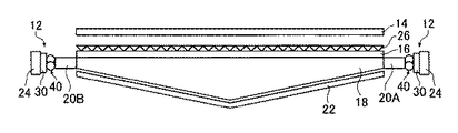
本発明の第1の実施形態に係るバックライトユニット2は、図1(A)、図1(B)、図2(A)及び図2(B)に示すように、2つの光源12と、拡散フィルム14と、偏光分離フィルム16と、導光部材としての導光板18と、光混合部20と、反射シート22とを有する。以下、バックライトユニット2を構成する各構成部品について説明する。
The
まず、光源12について説明する。
2つの光源12は、図1(B)に示されるように、それらの間に導光板18が挟まれるように配置される。光源12は、LEDアレイ24とカップリングレンズ40を備える。LEDアレイ24は、赤色、緑色及び青色の3種類の発光ダイオード(以下、それぞれR−LED32、G−LED34及びB−LED36という)を用いて形成される複数のRGB−LED30が一列に配置されて構成されている。図3に、複数のRGB−LED30の配置の様子を模式的に示す。図3に示すように、R−LED32、G−LED34及びB−LED36が規則的に配置されている。
また、図4に示すように、RGB−LED30は、R−LED32、G−LED34及びB−LED36からそれぞれ出射する光が所定の位置において交差するように、3種類のLED(R−LED32、G−LED34及びB−LED36)の光軸の向きが調整されている。このように3種類のLEDを調整することによって、それらLEDの光が混色されて白色光とされる。
このように、光源としてLEDを用いることで、光源から射出される光を後述する導光板のより奥まで届かせることができる。
3原色のLED(R−LED32、G−LED34及びB−LED36)を用いて構成されたRGB−LED30は、従来バックライト用光源として使用される冷陰極管(CCFL)と比較して色再現領域が広く色純度が高いため、このRGB−LED30をバックライト用光源として使用した場合には、従来よりも色再現性が高くなり、鮮やかな色彩の画像を表示することが可能になる。
First, the
As shown in FIG. 1B, the two
Further, as shown in FIG. 4, the RGB-
In this way, by using the LED as the light source, the light emitted from the light source can reach the back of the light guide plate described later.
The RGB-
図3及び図4に示すように、RGB−LED30の各LEDの光射出側にカップリングレンズとして3つのボールレンズ42、44及び46が配置されている。ボールレンズ42、44及び46は、各LEDに対応して配置されている。すなわち、1つのRGB−LED30について3つのボールレンズ42、44及び46が組み合わされて用いられている。各LED(R−LED32、G−LED34及びB−LED36)から出射した光は、ボールレンズ42、44及び46によって平行光にされる。そして、所定の位置で交わって白色光にされた後、導光板18の光混合部20に入射する。3つのボールレンズ42、44及び46を組み合わせて用いたカップリングレンズは、3軸を持ったレンズであり、RGB−LEDの各LEDの光を1点に絞り込んでミキシングすることができる。
ここでは、カップリングレンズとしてボールレンズを用いたが、これに限らず、LEDが発する光を平行光にすることができれば特に限定されない。カップリングレンズには、例えば、シリンドリカルレンズ、レンチキュラ、かまぼこ型のレンズ、フレネルレンズなどを用いることもできる。
As shown in FIGS. 3 and 4, three
Here, the ball lens is used as the coupling lens. However, the present invention is not limited to this, and the coupling lens is not particularly limited as long as the light emitted from the LED can be converted into parallel light. As the coupling lens, for example, a cylindrical lens, a lenticular, a kamaboko type lens, a Fresnel lens, or the like can be used.
次に、バックライトユニット2の導光板18について説明する。
導光板18は、図2(A)に示すように、略矩形形状の平坦な光射出面18aと、光射出面18aの反対側に位置し、光射出面18aの一辺に平行で、光射出面18aを2等分する2等分線Xに対して互いに対称で、光射出面18aに対して所定の角度で傾斜する2つの傾斜面(第1傾斜面18bと第2傾斜面18c)と、2つのLEDアレイ24に対向し、それらLEDアレイ24からの光が入射される2つの光入射面(第1光入射面18dと第2光入射面18e)とを有している。第1傾斜面18b及び第2傾斜面18cは、2等分線Xを境にして、光射出面18aに対し傾斜している。導光板18は、第1光入射面18d及び第2光入射面18eから中央に向かうに従って厚さが厚くなっており、中央部が最も厚く、両端部が最も薄くなっている。
つまり、導光板18は、略板状形状であり、光射出面18aが板の正面(面積の大きい面)、第1光入射面18d及び第2光入射面18eが板の側面(厚み方向の細長い面)、第1傾斜面18b及び第2傾斜面18cが板の裏面となる。
光射出面18aに対する第1傾斜面18b及び第2傾斜面18cの角度は特に限定されない。
また、第1傾斜面18b及び第2傾斜面18cには、光入射面18d及び18eと平行な方向にプリズム列が形成されている。このようなプリズム列の代わりに、プリズムに類する光学素子を規則的に形成することもできる。例えば、レンチキュラーレンズ、凹レンズ、凸レンズ、ピラミッド型など、レンズ効果を有する光学素子を導光板の傾斜面に形成することもできる。
Next, the
As shown in FIG. 2A, the
That is, the
The angles of the first
In addition, prism rows are formed on the first
図2に示す導光板18では、第1光入射面18d及び第2光入射面18eから入射した光は、導光板18の内部に含まれる散乱体(詳細は後述する)によって散乱されつつ、導光板18内部を通過し、直接、もしくは、第1傾斜面18b及び第2傾斜面18cで反射した後、光射出面18aから出射する。このとき、第1傾斜面18b及び第2傾斜面18cから一部の光が漏出する場合もあるが、漏出した光は導光板18の第1傾斜面18b及び第2傾斜面18cを覆うようにして配置される反射シート(図示せず)によって反射され再び導光板18の内部に入射する。
In the
導光板18は、透明樹脂に、光を散乱させるための散乱粒子が混錬分散されて形成されている。導光板18に用いられる透明樹脂の材料としては、例えば、PET(ポリエチレンテレフタレート)、PP(ポリプロピレン)、PC(ポリカーボネート)、PMMA(ポリメチルメタクリレート)、ベンジルメタクリレート、MS樹脂、あるいはCOP(シクロオレフィンポリマー)のような光学的に透明な樹脂が挙げられる。導光板18に混錬分散させる散乱粒子としては、アトシパール、シンコーン、シリカ、ジルコニア、誘電体ポリマなどを用いることができる。このような散乱粒子を導光板18の内部に含有させることによって、均一で輝度むらが少ない照明光を光出射面から出射することができる。
このような導光板18は、押出成形法や射出成形法を用いて製造することができる。
The
Such a
また、導光板18に含まれる散乱粒子の散乱断面積をΦ、光の入射する方向において導光板の光入射面から光射出面に直交する方向の厚みが最大となる位置までの長さ、本実施形態では、導光板の光の入射する方向(導光板18の第1光入射面18dに垂直な方向、以下「光軸方向」ともいう。)の半分の長さをLG、導光板18に含まれる散乱粒子の密度(単位体積あたりの粒子数)をNp、補正係数をKCとした場合に、Φ・Np・LG・KCの値が1.1以上であり、かつ8.2以下であり、さらに、補正係数KCの値が0.005以上0.1以下であるという関係を満たしている。導光板18は、このような関係を満たす散乱粒子を含んでいるので、均一で輝度むらが少ない照明光を光出射面から出射することができる。
Further, the scattering cross-sectional area of the scattering particles contained in the
一般的に、平行光束を等方媒質に入射させた場合の透過率Tは、Lambert−Beer則により下記式(1)で表される。
T=I/I0=exp(−ρ・x)・・・(1)
ここで、xは距離、I0は入射光強度、Iは出射光強度、ρは減衰定数である。
In general, the transmittance T when a parallel light beam is incident on an isotropic medium is expressed by the following formula (1) according to the Lambert-Beer rule.
T = I / I 0 = exp (−ρ · x) (1)
Here, x is a distance, I 0 is incident light intensity, I is outgoing light intensity, and ρ is an attenuation constant.
上記減衰定数ρは、粒子の散乱断面積Φと媒質に含まれる単位体積当たりの粒子数Npとを用いて下記式(2)で表される。
ρ=Φ・Np・・・(2)
したがって、導光板の光軸方向の半分の長さをLGとすると、光の取り出し効率Eoutは、下記式(3)で与えられる。ここで、導光板の光軸方向の半分の長さLGは、導光板18の光入射面に垂直な方向における導光板18の一方の光入射面から導光板18の中心までの長さとなる。
また、光の取り出し効率とは、入射光に対する、導光板の光入射面から光軸方向に長さLG離間した位置に到達する光の割合であり、例えば、図2に示す導光板18の場合は、端面に入射する光に対する導光板の中心(導光板の光軸方向の半分の長さとなる位置)に到達する光の割合である。
Eout∝exp(−Φ・Np・LG)・・・(3)
The attenuation constant ρ is expressed by the following equation (2) using the scattering cross-sectional area Φ of particles and the number of particles N p per unit volume contained in the medium.
ρ = Φ · N p (2)
Therefore, the length of the half of the optical axis direction of the light guide plate when the L G, the light extraction efficiency E out is given by the following equation (3). Here, half the length L G of the optical axis of the light guide plate, the length from one of the light incident surface of the
Furthermore, the light extraction efficiency and are, with respect to the incident light, the fraction of light reaching the position spaced the length L G in the optical axis direction from the light incident surface of the light guide plate, for example, the
E out ∝exp (−Φ · N p · L G ) (3)
ここで式(3)は有限の大きさの空間におけるものであり、式(1)との関係を補正するための補正係数KCを導入する。補正係数KCは、有限の空間の光学媒質中で光が伝搬する場合に経験的に求められる無次元の補正係数である。そうすると、光の取り出し効率Eoutは、下記式(4)で表される。
Eout=exp(−Φ・Np・LG・KC)・・・(4)
Here the formula (3) applies to a space of limited size, to introduce a correction coefficient K C for correcting the relationship between the expression (1). The compensation coefficient K C is a dimensionless compensation coefficient empirically obtained where light optical medium of limited dimensions propagates. Then, the light extraction efficiency E out is expressed by the following formula (4).
E out = exp (-Φ · N p · L G · K C) ··· (4)
式(4)に従えば、Φ・Np・LG・KCの値が3.5のときに、光の取り出し効率Eoutが3%であり、Φ・Np・LG・KCの値が4・7のときに、光の取り出し効率Eoutが1%である。
この結果より、Φ・Np・LG・KCの値が大きくなると、光の取り出し効率Eoutが低くなることが分かる。光は導光板の光軸方向へ進むにつれて散乱するため、光の取り出し効率Eoutが低くなると考えられる。
According to the equation (4), when the value of Φ · N p · L G · K C is 3.5, the light extraction efficiency E out is 3%, and Φ · N p · L G · K C When the value of is 4.7, the light extraction efficiency E out is 1%.
From this result, it is understood that the light extraction efficiency E out decreases as the value of Φ · N p · L G · K C increases. Since light is scattered as it travels in the direction of the optical axis of the light guide plate, the light extraction efficiency E out is considered to be low.
したがって、Φ・Np・LG・KCの値は大きいほど導光板として好ましい性質であることが分かる。つまり、Φ・Np・LG・KCの値を大きくすることで、光の入射面と対向する面から射出される光を少なくし、光射出面から射出される光を多くすることができる。すなわち、Φ・Np・LG・KCの値を大きくすることで、入射面に入射する光に対する光射出面から射出される光の割合(以下「光利用効率」ともいう。)を高くすることができる。具体的には、Φ・Np・LG・KCの値を1.1以上とすることで、光利用効率を50%以上にすることができる。
ここで、Φ・Np・LG・KCの値は大きくすると、導光板18の光射出面18aから出射する光の照度むらが顕著になるが、Φ・Np・LG・KCの値を8.2以下とすることで、照度むらを一定以下(許容範囲内)に抑えることができる。なお、照度と輝度は略同様に扱うことができる。従って、本発明においては、輝度と照度とは、同様の傾向があると推測される。
以上より、本発明の導光板のΦ・Np・LG・KCの値は、1.1以上かつ8.2以下であるという関係を満たすことが好ましく、2.0以上かつ7.0以下であることがより好ましい。また、Φ・Np・LG・KCの値は、3.0以上であればさらに好ましく、4.7以上であれば最も好ましい。
また、補正係数KCは、0.005以上0.1以下であることが好ましい。
Therefore, it can be seen that the larger the value of Φ · N p · L G · K C is, the more preferable property is for the light guide plate. In other words, by increasing the value of Φ · N p · L G · K C , it is possible to reduce the light emitted from the surface facing the light incident surface and increase the light emitted from the light emission surface. it can. That is, by increasing the value of Φ · N p · L G · K C, ( hereinafter also referred to as "light use efficiency".) Ratio of light emitted through the light exit plane to the light incident on the incident surface of the high can do. Specifically, by setting 1.1 or the value of Φ · N p · L G · K C, the light use efficiency can be 50% or more.
Here, when the value of Φ · N p · L G · K C is increased, the illuminance unevenness of the light emitted from the
Thus, the value of Φ · N p · L G · K C of the light guide plate of the present invention preferably satisfies the relationship of 1.1 or more and 8.2 or less, 2.0 or more and 7.0 The following is more preferable. The value of Φ · N p · L G · K C is more preferably as long as 3.0 or more, most preferably, not less than 4.7.
The correction coefficient K C is preferably 0.005 or more and 0.1 or less.
以下、具体例とともに、導光板についてより詳細に説明する。
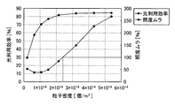
まず、散乱断面積Φ、粒子密度Np、導光板の光軸方向の半分の長さLG、補正係数KCを種々の値とし、Φ・Np・LG・KCの値が異なる各導光板について、計算機シミュレーションにより光利用効率を求め、さらに照度むらの評価を行った。ここで、照度むら[%]は、導光板の光射出面から射出される光の最大照度をIMaxとし、最小照度をIMinとし、平均照度をIAveとしたときの[(IMax−IMin)/IAve]×100とした。
測定した結果を下記表1に示す。また、表1の判定は、光利用効率が50%以上かつ照度むらが150%以下の場合を○、光利用効率が50%より小さいまたは照度むらが150%より大きいの場合を×として示す。
また、図5に、Φ・Np・LG・KCの値と光利用効率(光入射面に入射する光に対して光射出面から射出される光の割合)との関係を測定した結果を示す。
Hereinafter, the light guide plate will be described in more detail with specific examples.
First, the scattering cross section Φ, particle density N p , half length L G of the light guide plate in the optical axis direction, and correction coefficient K C are set to various values, and the values of Φ · N p · L G · K C are different. About each light-guide plate, the light use efficiency was calculated | required by computer simulation, and also illumination intensity nonuniformity was evaluated. Here, the illuminance unevenness [%] is the maximum illuminance of light emitted through the light exit plane of the light guide plate and I Max, a minimum illuminance and I Min, Average illuminance when the I Ave [(I Max - I Min ) / I Ave ] × 100.
The measured results are shown in Table 1 below. In the determination of Table 1, the case where the light use efficiency is 50% or more and the illuminance unevenness is 150% or less is indicated by ◯, and the case where the light use efficiency is less than 50% or the illuminance unevenness is more than 150% is indicated by x.
Further, in FIG. 5, to determine the relationship between Φ · N p · L G · K C values and light use efficiency (ratio of light emitted through the light exit surface for light incident on the light incident surface) Results are shown.

表1及び図5に示すように、Φ・Np・LG・KCを1.1以上とすることで、光利用効率を大きくすること、具体的には光利用効率を50%以上とすることができ、8.2以下とすることで、照度ムラを150%以下にすることができることがわかる。
また、Kcを0.005以上とすることで、光利用効率を高くすることができ、0.1以下とすることで、導光板からの射出される光の照度むらを小さくすることができることがわかる。
As shown in Table 1 and FIG. 5, by a Φ · N p · L G · K C to 1.1 or more, increasing the light use efficiency, specifically 50% or more of light use efficiency and It can be seen that by setting it to 8.2 or less, the illuminance unevenness can be reduced to 150% or less.
In addition, when Kc is set to 0.005 or more, the light use efficiency can be increased, and when it is set to 0.1 or less, the illuminance unevenness of light emitted from the light guide plate can be reduced. Recognize.
次に、導光板に混錬又は分散させる微粒子の粒子密度Npが種々の値の導光板を作成し、それぞれの導光板の光射出面の各位置から射出される光の照度分布を測定した。ここで本実施形態では、粒子密度Npを除いて他の条件、具体的には、散乱断面積Φ、導光板の光軸方向の半分の長さLG、補正係数KC、導光板の形状等は、同じ値とした。従って、本実施形態では、Φ・Np・LG・KCは、粒子密度Npに比例して変化する。
このようにして種々の粒子密度の導光板について、それぞれ光射出面から射出される光の照度分布を測定した結果を図6に示す。図6は、縦軸を照度[lx]とし、横軸を導光板の一方の光入射面からの距離(導光長)[mm]とした。
Then, the particle density N p of the particles which kneaded or dispersed in the light guide plate creates various values of the light guide plate was measured illuminance distribution of light emitted from the respective positions of the light emitting surface of each light guide plate . In this exemplary embodiment, other conditions except for the particle density N p, specifically, the scattering cross section [Phi, half the length of the optical axis direction of the light guide plate L G, the correction coefficient K C, the light guide plate The shape and the like were the same value. Accordingly, in the present embodiment, Φ · N p · L G · K C changes in proportion to the particle density N p.
FIG. 6 shows the result of measuring the illuminance distribution of the light emitted from the light exit surface for the light guide plates having various particle densities in this way. In FIG. 6, the vertical axis represents illuminance [lx], and the horizontal axis represents the distance (light guide length) [mm] from one light incident surface of the light guide plate.
さらに、測定した照度分布の導光板の側壁から射出される光の最大照度をIMaxとし、最小照度をIMinとし、平均照度をIAveとしたときの照度むら[(IMax−IMin)/IAve]×100[%]を算出した。
図7に、算出した照度むらと粒子密度との関係を示す。図7では、縦軸を照度むら[%]とし、横軸を粒子密度[個/m3]とした。また、図7には、横軸を同様に粒子密度とし、縦軸を光利用効率[%]とした、光利用効率と粒子密度との関係も併せて示す。
Furthermore, the illuminance unevenness when the maximum illuminance of the light emitted from the side wall of the light guide plate of the measured illuminance distribution is I Max , the minimum illuminance is I Min , and the average illuminance is I Ave [(I Max −I Min ) / I Ave ] × 100 [%] was calculated.
FIG. 7 shows the relationship between the calculated illuminance unevenness and the particle density. In FIG. 7, the vertical axis represents illuminance unevenness [%], and the horizontal axis represents particle density [pieces / m 3 ]. FIG. 7 also shows the relationship between the light utilization efficiency and the particle density, where the horizontal axis is similarly the particle density and the vertical axis is the light utilization efficiency [%].
図6、図7に示すように、粒子密度を高くする、つまりΦ・Np・LG・KCを大きくすると、光利用効率は高くなるが、照度むらも大きくなる。また、粒子密度を低くする、つまり、Φ・Np・LG・KCを小さくすると、光利用効率は低くなるが、照度むらを小さくなることがわかる。
ここで、Φ・Np・LG・KCを1.1以上8.2以下とすることで、光利用効率を50%以上とし、かつ、照度むらを150%以下とすることができる。照度むらを150%以下とすることで、照度むらを目立たなくすることができる。
つまり、Φ・Np・LG・KCを1.1以上8.2以下とすることで、光利用効率を一定以上とし、かつ照度むらも低減することができることがわかる。
As shown in FIGS. 6 and 7, when the particle density is increased, that is, Φ · N p · L G · K C is increased, the light use efficiency is increased, but the illuminance unevenness is also increased. It can also be seen that when the particle density is lowered, that is, when Φ · N p · L G · K C is reduced, the light utilization efficiency is reduced, but the illuminance unevenness is reduced.
Here, by the Φ · N p · L G · K C less than 1.1 and not greater than 8.2, the light use efficiency of 50% or more, and the illuminance unevenness of 150% or less. By setting the illuminance unevenness to 150% or less, the illuminance unevenness can be made inconspicuous.
That, Φ · N p · L G · K C to be to less than 1.1 and not greater than 8.2 yields light use efficiency above a certain level, and illuminance unevenness also seen that it is possible to reduce.
なお、本実施形態では、図1(B)及び図2(B)に示すように、光射出面18aを平坦な面としたが、本実施形態の場合も、光射出面が実質的に平坦(つまり、平面)であればよい。例えば、製造誤差または成形後の経時などにより、光射出面18aが第1傾斜面18d及び第2傾斜面18c側に多少の凹の曲面となった場合も実質的に平坦であれば、同様に用いることができる。
In this embodiment, as shown in FIG. 1B and FIG. 2B, the
ここで、導光板18は、光入射面となる第1光入射面18d、第2光入射面18eと、光射出面18aと、光反射面となる第1傾斜面18b、第2傾斜面18cの少なくとも1面の表面粗さRaを380nmより小さくすること、つまりRa<380nmとすることが好ましい。
光入射面となる第1光入射面18d、第2光入射面18eの表面粗さRaを380nmよりも小さくすることで、導光板表面の拡散反射を無視すること、つまり、導光板表面での拡散反射を防止することができ、入射効率を向上させることができる。
また、光射出面18aの表面粗さRaを380nmよりも小さくすることで、導光板表面の拡散反射透過を無視すること、つまり導光板表面での拡散反射透過を防止することができ、全反射により奥まで光を伝えることができる。
さらに、光反射面となる第1傾斜面18b、第2傾斜面18cの表面粗さRaを380nmよりも小さくすることで、拡散反射を無視すること、つまり光反射面での拡散反射を防止でき、全反射成分をより奥まで伝えることができる。
Here, the
By making the surface roughness Ra of the first
Further, by making the surface roughness Ra of the
Furthermore, by making the surface roughness Ra of the first
ここで、導光板は、光入射面における導光板の厚み(入光部厚み)をD1とし、光入射面と反対側の面における導光板の厚み(中心厚み)をD2とし、導光板の光の入射方向の長さ(導光長)をLとしたときに、
D1<D2 かつ、
27/100000<(D2−D1)/(L/2)<5/100 (A)
導光板の重量に対する混入された散乱粒子の重量の割合:Npaの範囲が
0.04%Wt<Npa<0.25%Wt
の関係を満たすことが好ましい。上記関係を満足する形状とすることで出射効率を30%以上に向上させることができる。
または、導光板は、
D1<D2 かつ、
66/100000<(D2−D1)/(L/2)<26/1000 (B)
導光板の重量に対する混入された散乱粒子の重量の割合:Npaの範囲が
0.04%Wt<Npa<0.25%Wt
の関係を満たすように改良することも好ましい。上記関係を満足する形状とすることで出射効率を40%以上に向上させることができる。
さらに、導光板は、
D1<D2 かつ、
1/1000<(D2−D1)/(L/2)<26/1000 (C)
導光板の重量に対する混入された散乱粒子の重量の割合:Npaの範囲が
0.04%Wt<Npa<0.25%Wt
の関係を満たすように改良することがさらに好ましい。上記関係を満足する形状とすることで、出射効率を50%以上に向上させることができる。
Here, in the light guide plate, the thickness of the light guide plate on the light incident surface (light incident portion thickness) is D1, and the thickness of the light guide plate on the surface opposite to the light incident surface (center thickness) is D2. When the length in the incident direction (light guide length) is L,
D1 <D2 and
27/100000 <(D2-D1) / (L / 2) <5/100 (A)
Ratio of mixed scattering particle weight to light guide plate weight: Npa range is 0.04% Wt <Npa <0.25% Wt
It is preferable to satisfy the relationship. By making the shape satisfying the above relationship, the emission efficiency can be improved to 30% or more.
Or the light guide plate
D1 <D2 and
66/100000 <(D2-D1) / (L / 2) <26/1000 (B)
Ratio of mixed scattering particle weight to light guide plate weight: Npa range is 0.04% Wt <Npa <0.25% Wt
It is also preferable to improve so as to satisfy this relationship. By making the shape satisfying the above relationship, the emission efficiency can be improved to 40% or more.
Furthermore, the light guide plate
D1 <D2 and
1/1000 <(D2-D1) / (L / 2) <26/1000 (C)
Ratio of mixed scattering particle weight to light guide plate weight: Npa range is 0.04% Wt <Npa <0.25% Wt
It is further preferable to improve so as to satisfy the relationship. By making the shape satisfying the above relationship, the emission efficiency can be improved to 50% or more.
図8に、傾斜面の傾斜角がそれぞれ異なる導光板、つまり(D2−D1)/(L/2)が異なる種々の形状の導光板についてそれぞれ光利用効率を測定した結果を示す。ここで、図8の横軸は、導光板の(D2−D1)/(L/2)であり、縦軸は、光利用効率[%]である。
図8に示した測定結果からも、導光板の形状を27/100000<(D2−D1)/(L/2)<5/100とすることで、光利用効率を30%以上とすることができ、66/100000<(D2−D1)/(L/2)<26/1000とすることで、光利用効率を40%以上とすることができ、1/1000<(D2−D1)/(L/2)<26/1000とすることで、光利用効率を50%以上とすることができることがわかる。
FIG. 8 shows the results of measuring the light utilization efficiency for light guide plates having different inclination angles of the inclined surfaces, that is, light guide plates having various shapes with different (D2-D1) / (L / 2). Here, the horizontal axis of FIG. 8 is (D2-D1) / (L / 2) of the light guide plate, and the vertical axis is the light utilization efficiency [%].
From the measurement results shown in FIG. 8, the light utilization efficiency can be increased to 30% or more by setting the shape of the light guide plate to 27/100000 <(D2-D1) / (L / 2) <5/100. By using 66/100000 <(D2-D1) / (L / 2) <26/1000, the light utilization efficiency can be increased to 40% or more, and 1/1000 <(D2-D1) / ( It can be seen that the light utilization efficiency can be 50% or more by setting L / 2) <26/1000.
ここで、本実施形態では、光を効率よく反射させるために導光板18の2つの傾斜面(第1傾斜面18b及び第2傾斜面18c)にプリズム列を形成したが、必ずしも形成する必要はなく、微細な凹凸を形成していない平坦な面としてもよい。
Here, in the present embodiment, the prism rows are formed on the two inclined surfaces (the first
また、本実施形態では、導光板を、光射出面に対向する面を光射出面に対して一定角度傾斜した傾斜面と形状としたが、本発明は、これに限定されず光入射面における導光板の厚みよりも、光入射面に対向する面における導光板の厚みが厚い形状であれば、どのような形状でもよい。例えば、導光板の光射出面に対向する面(図1及び図2の第1傾斜面18b及び/または第2傾斜面18c)を曲面形状としてもよい。また、傾斜面を曲面とする場合は、光射出面側に凸の形状としても、光射出面に凹の形状としてもよい。
In the present embodiment, the light guide plate has a shape that is an inclined surface in which a surface facing the light emitting surface is inclined at a certain angle with respect to the light emitting surface. Any shape may be used as long as the thickness of the light guide plate on the surface facing the light incident surface is thicker than the thickness of the light guide plate. For example, the surface (the first
以下、図9とともに導光板のより好ましい形状の一例を説明する。
図9(A)〜図9(D)は、それぞれ導光板の他の一例を示す概略断面図である。また、図10(A)は、導光板の他の一例を示す概略断面図であり、図10(B)は、図10(A)に示す導光板の傾斜面同士の接続部周辺を拡大して示す概略断面図である。
図9(A)に示す導光板202は、第1傾斜面204が、光入射面18d側の第1傾斜部206と、導光板中心側の第2傾斜部208とで構成されている。第1傾斜部206と第2傾斜部208とは、光射出面に対する傾斜角が互いに異なる角度で傾斜し、第1傾斜部206の傾斜角よりも第2傾斜部208の傾斜角の方が角度が小さい。つまり、第1傾斜面は、導光板中心に向かうに従って傾斜角が緩やかになる傾斜部で形成されている。
また、第2傾斜面204’は、第1傾斜面204と対称な形状であり、第2光入射面18e側の第1傾斜部206’と導光板中心側で第1傾斜部206’よりも傾斜角が緩やかな第2傾斜部208’とで構成されている。
このように、傾斜面の断面形状を、傾斜角の異なる複数の直線で構成される形状とし、中心側の傾斜部の傾斜角よりも光入射面側の傾斜部の傾斜角の方が大きくなる形状とすることで、光射出面の光入射面近傍部分から射出される光の輝度が高くなることを防止できる。これにより、より均一な光を光射出面から射出させることができる。
また、図9(A)では、傾斜面を2つの傾斜部で構成したが、傾斜面を構成する傾斜部の数は特に限定されず、導光板の中心に向かうに従って傾斜角が徐々に緩やかになるように配置した任意の数の傾斜部で構成することができる。
例えば、図9(B)に示すように、導光板210の第1傾斜面212(第2傾斜面212’)を第1光入射面18d(第2光入射面18e)側から導光板中心に向かって、第1傾斜部214(214’)と、第1傾斜部214(214’)よりも傾斜角が緩やかな第2傾斜部216(216’)と、第2傾斜部216(216’)よりも傾斜角が緩やかな第3傾斜部218(218’)の3つの傾斜部で構成してもよい。
Hereinafter, an example of a more preferable shape of the light guide plate will be described with reference to FIG.
FIG. 9A to FIG. 9D are schematic cross-sectional views illustrating other examples of the light guide plate. 10A is a schematic cross-sectional view showing another example of the light guide plate, and FIG. 10B is an enlarged view of the periphery of the connecting portion between the inclined surfaces of the light guide plate shown in FIG. It is a schematic sectional drawing shown.
In the
Further, the second
In this way, the cross-sectional shape of the inclined surface is configured by a plurality of straight lines having different inclination angles, and the inclination angle of the inclined portion on the light incident surface side is larger than the inclination angle of the inclined portion on the center side. By adopting the shape, it is possible to prevent the luminance of the light emitted from the portion near the light incident surface of the light emitting surface from increasing. Thereby, more uniform light can be emitted from the light exit surface.
In FIG. 9A, the inclined surface is configured by two inclined portions, but the number of inclined portions constituting the inclined surface is not particularly limited, and the inclination angle gradually decreases toward the center of the light guide plate. It can be configured by an arbitrary number of inclined portions arranged to be.
For example, as shown in FIG. 9B, the first inclined surface 212 (second
次に、図9(C)に示す導光板220は、第1傾斜面222の第1光入射面18d側、つまり、第1光入射面18dとの接続部にR形状の曲面部222aを有する。また、第2傾斜面222’も同様に第2光入射面18e側にR形状の曲面部222a’を有する。
このように、導光板の傾斜面の光入射面との接続部に曲面部を設けR形状とし、光入射面と傾斜面とを滑らかに接続された形状とすることによっても、光射出面の光入射面近傍部分から射出する光の輝度が高くなることを防止できる。
Next, the
As described above, the curved surface portion is provided in the connection portion between the light incident surface and the light incident surface of the light guide plate to form an R shape, and the light incident surface and the inclined surface are smoothly connected to each other. It is possible to prevent the brightness of light emitted from the vicinity of the light incident surface from increasing.
次に、図9(D)に示す導光板230は、第1傾斜面232及び第2傾斜面232’が10次多項式で表すことができる非球面形状に形成されている。
このように傾斜面を非球面形状とすることによっても、光射出面の光入射面近傍部分から射出する光の輝度が高くなることを防止できる。
Next, in the
By making the inclined surface into an aspherical shape in this way, it is possible to prevent the luminance of light emitted from a portion near the light incident surface of the light emitting surface from increasing.
さらに、図10(A)及び図10(B)に示すように、導光板60は、第1傾斜面60bと第2傾斜面60cとの接続部60f(導光板の傾斜面の中央部)を曲面形状またはR形状とし、滑らかに接続させることが好ましい。つまり、導光板の傾斜面は、2等分線に垂直な断面において、2等分線側が曲線(より具体的には、円弧)で、かつ、光入射面側が直線となる形状することが好ましい。
これにより、第1傾斜面60bと第2傾斜面60cとの接続部60fで輝線、暗線等が発生することを防止でき、より均一な光を射出させることができる。
Further, as shown in FIGS. 10A and 10B, the
As a result, bright lines, dark lines, and the like can be prevented from being generated at the connecting
ここで、導光板60の傾斜面60b,60c同士の接続部60f、つまり導光板60の中央部をR形状とする場合は、そのR形状の曲率半径をR1とすると、曲率半径R1と導光板の光の入射方向の長さLとの関係が、3L≦R1≦500Lを満たすことが好ましい。
また、接続部60fのR形状の、光の入射方向における端部から端部までの長さをLRとし、光射出面60aに平行な面と第1傾斜面60b(または、第2傾斜面60c)とでなす角をθとしたとき、2R1・sin(θ)≦LRを満たすことが好ましい。
LRを2R1・sin(θ)以上とすることで、中央部の輝度の低下を抑制することができ、光射出面からより均一な光を射出させることができる。
また、LRは、0.98以下とすることが好ましい。これにより、本発明の効果をより好適にえることができる。
さらに、導光板は、3L≦R1≦500L、かつ、2R1・sin(θ)≦LR≦0.98Lを満たす形状であることがより好ましい。
Here, the
In addition, the length of the R-shape of the
By setting LR to be 2R 1 · sin (θ) or more, it is possible to suppress a decrease in luminance at the central portion and to emit more uniform light from the light exit surface.
LR is preferably 0.98 or less. Thereby, the effect of the present invention can be obtained more suitably.
Furthermore, it is more preferable that the light guide plate has a shape satisfying 3L ≦ R 1 ≦ 500L and 2R 1 · sin (θ) ≦ L R ≦ 0.98L.
なお、θは、導光板60の最大厚みtmaxと、最小厚みtmin及び導光板の光の入射方向の長さLとを用いて、下記式(D)として表すことができる。
![]()
![]()
また、上記の透明樹脂に可塑剤を混入して導光板を作製してもよい。
このように、透明材料と可塑剤とを混合した材料で導光板を作製することで、導光板をフレキシブルにすること、つまり、柔軟性のある導光板とすることができ、導光板を種々の形状に変形させることが可能となる。従って、導光板の表面を種々の曲面に形成することができる。
これにより、例えば、導光板、または、この導光板を用いた面状照明装置を電飾(イルミネーション)関係の表示板として用いる場合に、曲率を持つ壁にも装着することが可能となり、導光板をより多くの種類、より広い使用範囲の電飾やPOP(POP広告)等に利用することができる。
Moreover, you may produce a light-guide plate by mixing a plasticizer in said transparent resin.
Thus, by producing a light guide plate with a material in which a transparent material and a plasticizer are mixed, the light guide plate can be made flexible, that is, a flexible light guide plate. It can be deformed into a shape. Therefore, the surface of the light guide plate can be formed into various curved surfaces.
Accordingly, for example, when a light guide plate or a planar lighting device using the light guide plate is used as a display plate related to illumination (illumination), the light guide plate can be attached to a wall having a curvature. Can be used for more types, lighting of a wider range of use, POP (POP advertising), and the like.
ここで、可塑剤としては、フタル酸エステル、具体的には、フタル酸ジメチル(DMP)、フタル酸ジエチル(DEP)、フタル酸ジブチル(DBP)、フタル酸ジ−2−エチルヘキシル(DOP(DEHP))、フタル酸ジノルマルオクチル(DnOP)、フタル酸ジイソノニル(DINP)、フタル酸ジノニル(DNP)、フタル酸ジイソデジル(DIDP)、フタル酸混基エステル(C6〜C11)(610P、711P等)、フタル酸ブチルベンジル(BBP)が例示される。また、フタル酸エステル以外にも、アジピン酸ジオクチル(DOA)、アジピン酸ジイソノニル(DINA)、アジピン酸ジノルマルアルキル(C6、8、10)(610A)、アジピン酸ジアルキル(C7、9)(79A)、アゼライン酸ジオクチル(DOZ)、セバシン酸ジブチル(DBS)、セバシン酸ジオクチル(DOS)、リン酸トリクレシル(TCP)、アセチルクエン酸トリブチル(ATBC)、エポキシ化大豆油(ESBO)、トリメリット酸トリオクチル(TOTM)、ポリエステル系、塩素化パラフィン等が例示される。 Here, as the plasticizer, phthalate ester, specifically, dimethyl phthalate (DMP), diethyl phthalate (DEP), dibutyl phthalate (DBP), di-2-ethylhexyl phthalate (DOP (DEHP)) ), Di-normal octyl phthalate (DnOP), diisononyl phthalate (DINP), dinonyl phthalate (DNP), diisodecyl phthalate (DIDP), phthalic acid mixed ester (C 6 to C 11 ) (610P, 711P, etc.) And butylbenzyl phthalate (BBP). In addition to the phthalate ester, dioctyl adipate (DOA), diisononyl adipate (DINA), dinormal alkyl adipate (C6, 8, 10 ) (610A), dialkyl adipate (C7, 9 ) ( 79A), dioctyl azelate (DOZ), dibutyl sebacate (DBS), dioctyl sebacate (DOS), tricresyl phosphate (TCP), tributyl acetylcitrate (ATBC), epoxidized soybean oil (ESBO), trimellitic acid Examples include trioctyl (TOTM), polyester, and chlorinated paraffin.
図1及び図2に示すように、本実施形態のバックライトユニット2では、導光板18の両方の側面に密着して光混合部20A及び20Bが設けられている。光混合部20A及び20Bは、透明な樹脂に、光を散乱する粒子が混入された柱状の光学部品であり、カップリングレンズ40を介して入射される光をミキシングする機能を有する。光混合部20A及び20Bの材料には、基本的には、導光板18と同じ材料を用いることができ、導光板18と同様に、内部に光を散乱させるための散乱体を含むことができる。光混合部20A及び20Bの内部に含有させる散乱体の密度等は、導光板18と同じであっても異なっていても良い。また、光混合部20A及び20Bは、図2に示されるように、LEDアレイ24に近接して配置されるため、耐熱性の高い材料を用いて形成されることが好ましい。
As shown in FIGS. 1 and 2, in the
次に、偏光分離フィルム16について説明する。
本実施形態においては、好ましい形態として、導光板18の光射出側の面である光射出面18aの上に偏光分離フィルム16が導光板18と一体化して形成されている。偏光分離フィルム16は、導光板の光射出面から出射する光のうち、所定の偏光成分、例えば、p偏光成分を選択的に透過させ、それ以外の偏光成分、例えば、s偏光成分の殆どを反射させることができる。偏光分離フィルム16は、反射した光を導光板に再度入射させて、再利用することができるので、光の利用効率を高め、輝度を格段に向上させることができる。
偏光分離フィルム16は、例えば、透明樹脂に針状粒子を混錬して分散させて得られた板材を延伸させて、針状粒子を所定の方向に配向させることによって得られる。
偏光分離フィルム16は、導光板18の製造時に圧着又は融着させて一体化させることが好ましい。これにより、導光板18の光射出面18aと偏光分離フィルム16との間に空気を介在させることなく、互いを密着させることができる。
ここでは、偏光分離フィルム16を導光板18と一体で形成したが、これに限定されず、偏光分離フィルム16と導光板18とをそれぞれ独立に製造し、導光板18の光射出側の面に偏光分離フィルム16を貼り付けて設けても良い。
また、図示例では、偏光分離フィルム16を導光板18の光射出面の直上に設けたが、これに限定されず、拡散フィルムの上に設けることもできる。この場合、偏光分離フィルムを拡散フィルムと一体にしてもよい。
Next, the
In the present embodiment, as a preferred embodiment, the
The polarized
The polarized
Here, the
In the illustrated example, the
また、偏光分離フィルム16としては、公知のものを用いることができる。
例えば、特開平6−331824号公報に記載されているような、少なくとも1偏波面に対しては、導光板の光射出面に導光板の屈折率よりも高い屈折率を有し、この偏波面に直交する偏波面に対しては導光板の平均屈折率より低い屈折率を有する複屈折性材料を用いることもできる。
また、特開平11−281975号公報に記載されているような、延伸フィルムを用いることもできる。ここで、延伸フィルムを用いる場合は、特開平11−281975号公報に記載されているように、粘着剤層あるいは接着剤層を介して、導光板の片面に貼付することが好ましい。
また、特開平7−49496号公報に記載されているような、相対的に屈折率の大きな透明性媒質と相対的に屈折率の小さな透明性媒質とを交互に積層してなる多層構造体や、面状透明性支持体の少なくとも片方の面に、好ましくは1000nm以下の厚みを有する誘電体膜が少なくとも一層以上成膜されているもの、もしくは屈折率の異なる複数種類の透明複数種類の透明性ポリマーが積層されたものを用いることもできる。
また、特開平7−72475号公報に記載されているような、断面略W字状の透明支持体に可視光波長と同等以下の厚みを有する誘電薄膜を少なくとも一層以上設けたものからなり、所定の入射方向の近傍の光線についてp偏光成分を透過し、s偏光成分の少なくとも一部を反射する偏光分離器を用いることもできる。
また、特開2004−78234号公報に記載されているような、並んで配列された本質的に直角の2等辺の係数のプリズムの直線的な配列からなる構造化表面を有し、この構造表面と反対の平滑な表面への接面に関してほぼ45°の角度を形成する垂直な係数の面を有する第1の材料と、本質的に第1の材料と同じ第2の材料と、少なくとも1つの材料の構造化平面上にあり、選択された光学的な厚さの高屈折率材料及び低屈折率材料の交互に重なる層からなる少なくとも1つの光学的な堆積とからなり、第1及び第2の材料は、全て光学的に接合され、単一ユニットを形成し、この単一ユニットにおいて、第1及び第2の材料の屈折率及び上記光学的堆積の複数の層の上記屈折率及び光学的厚さは、偏光された光の選択的な反射を生成するように全て選ばれて、上記光学的な堆積の一部の内部において、混合された偏光の入射光線が、s−偏光成分及びp−偏光成分に分離され、上記s−偏光成分は、上記光学的な堆積の他の部分で反射され、その部分で入射光線に平行に反射されるが、入射光と逆の方向に進み、上記p−偏光成分は、入射光線に対して平行に透過する再帰反射偏光子を用いることもできる。
また、特開昭61−262705号公報に記載されているような、A型の凸条とV型の溝を交互に設け三角波形面を形成した透明な材料の上に偏光フィルタ機能や位相差板機能を有する誘電体多層膜を設けた偏光素子を用いることもできる。
また、米国特許第3610729号明細書に記載されているような、複屈折性を備える材料を種々の波長の1/4となる厚みの層にして連続的に積層させた偏光フィルムを用いることもできる。
また、米国特許第5867316号明細書に記載されているような、複屈折性を備える連続相と連続相の内部に少量の分散相とを有するポリマーにより形成された光学フィルムを用いることもできる。
また、特開2003−295183号公報に記載されているような、表面プラズモンを利用した金属薄膜を低屈折率透明媒質でサンドイッチした構成の偏光分離膜を用いることもできる。
さらに、入射面に平行なP偏光成分のみを透過し、入射面に垂直なS偏光成分を反射する表面プラズモンを利用した偏光分離膜の配置に加え、光の偏光方向を変更する、例えば直交する偏光成分の間に光学的な厚さにおいてλ/4の差を生じる僅かな複屈折性を有するλ/4位相フィルムや拡散フィルムなどの偏光方向変更膜を導光板と一体にして構成することにより、輝度をより向上させることができる。
Moreover, as the
For example, as described in JP-A-6-331824, for at least one polarization plane, the light exit surface of the light guide plate has a refractive index higher than the refractive index of the light guide plate. A birefringent material having a refractive index lower than the average refractive index of the light guide plate can be used for the plane of polarization orthogonal to.
Moreover, a stretched film as described in JP-A-11-281975 can also be used. Here, when using a stretched film, as described in JP-A-11-281975, it is preferable that the stretched film is attached to one side of the light guide plate via an adhesive layer or an adhesive layer.
Moreover, as described in JP-A-7-49496, a multilayer structure in which transparent media having a relatively high refractive index and transparent media having a relatively low refractive index are alternately laminated, In addition, at least one dielectric film having a thickness of preferably 1000 nm or less is formed on at least one surface of the planar transparent support, or a plurality of types of transparent types having different refractive indexes What laminated | stacked the polymer can also be used.
Further, as described in JP-A-7-72475, a transparent support having a substantially W-shaped cross section is provided with at least one dielectric thin film having a thickness equal to or less than a visible light wavelength, and a predetermined thickness. It is also possible to use a polarization separator that transmits the p-polarized component and reflects at least a part of the s-polarized component with respect to the light rays in the vicinity of the incident direction.
And a structured surface comprising a linear array of essentially right-angled isosceles prisms arranged side by side as described in Japanese Patent Application Laid-Open No. 2004-78234. A first material having a plane of perpendicular modulus forming an angle of approximately 45 ° with respect to the tangent to the opposite smooth surface, a second material essentially the same as the first material, and at least one Comprising at least one optical deposit of alternating layers of a high refractive index material and a low refractive index material of a selected optical thickness on a structured plane of the material, the first and second Are all optically bonded to form a single unit in which the refractive index of the first and second materials and the refractive index and optical properties of the plurality of layers of the optical deposition. Thickness produces selective reflection of polarized light In all of the optical deposits, the mixed polarized incident light is separated into an s-polarized component and a p-polarized component, and the s-polarized component is Reflected by other parts of the typical deposit and reflected parallel to the incident light in that part, but proceeding in the opposite direction to the incident light and the p-polarized component is transmitted parallel to the incident light. A reflective polarizer can also be used.
Further, as described in JP-A-61-262705, a polarizing filter function and a phase difference are formed on a transparent material in which A-shaped ridges and V-shaped grooves are alternately provided to form a triangular waveform surface. A polarizing element provided with a dielectric multilayer film having a plate function can also be used.
In addition, a polarizing film as described in US Pat. No. 3,610,729 can be used by continuously laminating a material having birefringence into a layer having a thickness of ¼ of various wavelengths. it can.
Further, as described in US Pat. No. 5,867,316, an optical film formed of a polymer having a continuous phase having birefringence and a small amount of a dispersed phase inside the continuous phase can also be used.
Further, a polarization separation film having a structure in which a metal thin film using surface plasmon is sandwiched with a low refractive index transparent medium as described in JP-A-2003-295183 can also be used.
Furthermore, in addition to the arrangement of the polarization separation film using surface plasmons that transmit only the P-polarized light component parallel to the incident surface and reflect the S-polarized light component perpendicular to the incident surface, the polarization direction of the light is changed, for example, orthogonal By forming a polarization direction changing film such as a λ / 4 phase film or a diffusion film having a slight birefringence that causes a difference of λ / 4 in the optical thickness between the polarization components with the light guide plate. , The luminance can be further improved.
また、特開平8−76114号公報に記載されているような、液晶と高分子の複合体を延伸して形成した異方性散乱体を用いた散乱型偏光フィルムを偏光分離フィルム16の代わりに用いたり、特開平6−281814号公報に記載されているような、分子螺旋の軸がフィルムを横切って延在するように配向させ、フィルムにおける分子螺旋のピッチが、最大ピッチと最小ピッチとの間の差が少なくとも100nmとなるように変化されているコレスティック型偏光フィルムを偏光分離フィルム16として用いてもよい。
また、特開2001−343612号公報に記載されているような、直線偏光の振動方向によりヘイズの値が異なるヘイズ異方性層を用いることもできる。この場合は、さらに、導光板の光射出面と反対面に第一位相差板を貼付し、かつ導光板と反射板との間に第2位相差板を設置することが好ましい。
また、特開平9−274108号公報に記載されているような、透明な高分子フィルムの中にこれと異なる材料からなる微小領域が一様に分散され、高分子フィルムと微小領域とは直交する直線偏光の一方に対する屈折率がほぼ同じで、該直線偏光の他方に対する屈折率が異なる偏光素子を用いることができる。
A scattering type polarizing film using an anisotropic scatterer formed by stretching a composite of a liquid crystal and a polymer as described in JP-A-8-76114 is used instead of the
Also, a haze anisotropic layer having a different haze value depending on the vibration direction of linearly polarized light as described in JP-A-2001-343612 can be used. In this case, it is further preferable to attach a first retardation plate to the surface opposite to the light exit surface of the light guide plate, and to install a second retardation plate between the light guide plate and the reflection plate.
Further, as described in JP-A-9-274108, minute regions made of a different material are uniformly dispersed in a transparent polymer film, and the polymer film and the minute regions are orthogonal to each other. Polarization elements having substantially the same refractive index for one of the linearly polarized light and different refractive indexes for the other of the linearly polarized light can be used.
上記実施形態では、偏光分離フィルムを導光板18の光射出面側に設けて輝度の向上を実現させたが、偏光分離フィルムを設ける代わりに、特開2001−201746公報、特開2001−228474号公報に記載されているように、導光板の光射出面に偏光分離機能を有する微細凹凸部を形成することでも、光射出面から射出させる光の輝度を向上させることができる。
また、偏光分離フィルム16の代わりに、特開平9−134607号公報に記載されているように、導光板と反射部材(反射板)との間に、実質的に導光板の屈折率以上の第1の屈折率及び導光板の屈折率よりも小さな第2の屈折率を有し、第1の偏光状態の略全てを、第1の偏光状態に直交する第2の偏光状態から分離する異方性層を配置することでも輝度を向上させることができる。
また、特開2004−363062号公報に記載されているように、導光板の傾斜背面に、微細突起からなり、偏光分離機能を有する粗面パターンを形成することでも、輝度を向上させることができる。
また、特表平10−508151号公報に記載されているように、光導波路(導光板)に、光導波路の材料と異なる材料が充填された凹部を設け、この2つの材料の一方を屈折率がnpである等方性材料とし、他方の材料を屈折率がnoとneである異方性材料とする。ここで、屈折率に関しては、noまたはneがnpに等しいかまたは事実上等しくする。これにより、等方性材料と異方性材料間の境界面で偏光を分離させることができ、光源で照射された光の大部分を光導波路より出る前に同じ偏光方向を有する光に変えることができる。このように、特表平10−508151号公報に記載されている構成を本発明に適用することによっても輝度を向上させることができる。
また、特開平9−292530号公報に記載されているように、導光板を導光機能を有する2層以上の層で構成し、第1の層または第2の層の少なくとも一方の層を複屈折性を有する材料とし、第1の層と第2の層との間に界面を設け、界面で光が散乱または屈折または回折した光を導光板の表面から出射させることによっても輝度を向上させることができる。
In the above embodiment, the polarization separation film is provided on the light exit surface side of the
Further, instead of the
In addition, as described in Japanese Patent Application Laid-Open No. 2004-363062, the luminance can also be improved by forming a rough surface pattern that is formed of fine protrusions and has a polarization separation function on the inclined back surface of the light guide plate. .
Further, as described in JP-A-10-508151, a concave portion filled with a material different from the material of the optical waveguide is provided in the optical waveguide (light guide plate), and one of these two materials has a refractive index. Is an isotropic material with np, and the other material is an anisotropic material with refractive indices no and ne. Here, regarding the refractive index, no or ne is equal to or substantially equal to np. As a result, polarized light can be separated at the interface between the isotropic material and the anisotropic material, and most of the light irradiated by the light source is changed to light having the same polarization direction before exiting the optical waveguide. Can do. Thus, the luminance can also be improved by applying the configuration described in JP-T-10-508151 to the present invention.
Further, as described in JP-A-9-292530, the light guide plate is composed of two or more layers having a light guide function, and at least one of the first layer and the second layer is duplicated. The brightness is also improved by using a refractive material, providing an interface between the first layer and the second layer, and emitting light scattered, refracted, or diffracted from the surface of the light guide plate at the interface. be able to.
次に、バックライトユニットの反射シート22について説明する。
反射シート22は、導光板18の傾斜面18c、18dから漏洩する光を反射して、再び導光板18に入射させるものであり、光の利用効率を向上させることができる。反射シート22は、導光板18の傾斜面18c及び18dをそれぞれ覆うように中央部で折り曲げられて形成される。
反射シート22は、導光板18の傾斜面18c、18dから漏洩する光を反射することができるものであれば、どのような材料で形成されてもよく、例えば、PETやPP(ポリプロピレン)等にフィラーを混練後延伸することによりボイドを形成して反射率を高めた樹脂シート、透明もしくは白色の樹脂シート表面にアルミ蒸着などで鏡面を形成したシート、アルミ等の金属箔もしくは金属箔を担持した樹脂シート、あるいは表面に十分な反射性を有する金属薄板により形成することができる。
Next, the
The
The
次に、拡散フィルム14について説明する。
拡散フィルム14は、図1に示されるように、偏光分離フィルム16と液晶パネル4との間に配置される。拡散フィルム14は、フィルム状部材に光拡散性を付与して形成される。フィルム状部材は、例えば、PET(ポリエチレンテレフタレート)、PP(ポリプロピレン)、PC(ポリカーボネート)、PMMA(ポリメチルメタクリレート)、ベンジルメタクリレート、MS樹脂、あるいはCOP(シクロオレフィンポリマー)のような光学的に透明な樹脂を材料に形成することができる。
拡散フィルム14の製造方法は特に限定されないが、例えば、フィルム状部材の表面に微細凹凸加工や研磨による表面粗化を施して拡散性を付与したり、表面に光を散乱させるシリカ、酸化チタン、酸化亜鉛等の顔料や、樹脂、ガラス、ジルコニア等のビーズ類をバインダとともに塗工したり、上記顔料やビーズ類を上記透明な樹脂中に混練したりすることで形成することができる。他には、反射率が高く光の吸収が低い材料で、例えば、Ag、Alのような金属を用いて形成することもできる。
本発明において、拡散フィルム14としては、マットタイプやコーティングタイプの拡散フィルムを用いることができる。
Next, the
As shown in FIG. 1, the
Although the manufacturing method of the
In the present invention, the
拡散フィルム14は、導光板18の光射出面から所定の距離だけ離して配置されてもよく、その距離は導光板18の光射出面からの光量分布に応じて適宜変更することができる。
このように拡散フィルム14を導光板18の光射出面から所定の間隔だけ離すことにより、導光板18の光射出面から射出する光が、光射出面と拡散フィルム14の間で更にミキシング(混合)される。これにより、拡散フィルム14を透過して液晶表示パネル4を照明する光の輝度を、より一層均一化することができる。
拡散フィルム14を導光板18の光射出面から所定の間隔だけ離す方法としては、例えば、拡散フィルム14と導光板18との間にスペーサを設ける方法などを用いることができる。
The
Thus, by separating the
As a method of separating the
以上、本発明の第1の実施形態のバックライトユニット2の各構成要素について詳細に説明したが、本発明はこれに限定されるものではない。
例えば、LEDから射出された光を混合することができるため混合部、さらには、射出された光を平行光とすることができるためボールレンズ、シリンドリカルレンズ等の平行光生成機構を設けることが好ましいが、混合部及び平行光生成機構は、必ずしも設ける必要はない。
また、混合部及び/または平行光生成機構は、光源及び導光板と非接触で設けることが好ましい。混合部及び/または平行光生成機構を光源及び導光板と非接触で配置することで、光源から生じる熱が混合部、平行光生成機構さらには導光板に伝わり、熱により変形することを防止できる。これにより、光射出面から射出される光に輝度むらが生じることをより確実に防止することができる。
As mentioned above, although each component of the
For example, the light emitted from the LED can be mixed, and therefore, it is preferable to provide a mixing unit, and further, a parallel light generation mechanism such as a ball lens or a cylindrical lens is provided since the emitted light can be converted into parallel light. However, the mixing unit and the parallel light generation mechanism are not necessarily provided.
Moreover, it is preferable to provide a mixing part and / or a parallel light production | generation mechanism in a non-contact with a light source and a light-guide plate. By disposing the mixing unit and / or the parallel light generation mechanism in a non-contact manner with the light source and the light guide plate, heat generated from the light source can be transmitted to the mixing unit, the parallel light generation mechanism and the light guide plate, and can be prevented from being deformed by the heat. . Thereby, it is possible to more surely prevent uneven brightness from occurring in the light emitted from the light exit surface.
上記実施の形態では、赤色、緑色及び青色の3色のLED32、34及び36を用い、カップリングレンズ40により各LEDが発する光を混色し白色光を得たが、本発明はこれに限定されない。光源には、1種類のLEDと蛍光物質(つまり、蛍光体)とを組み合わせ、LEDが発する光を蛍光物質により白色光に変換するように構成したLEDチップを用いてもよい。例えば、単色のLEDとしてGaN系青色LEDを用いた場合には、YAG(イットリウム・アルミニウム・ガーネット)系蛍光物質を用いれば、白色光を得ることができる。
このような白色光を得ることができる光源を利用すれば、レンズを利用する必要がなくなり部材の数を削減することができる。
また、光源として1種類のLEDを用いた場合でも、光源としてLEDを用いることで、光源から射出される光を後述する導光板のより奥まで届かせることができる。これにより、装置の薄型を維持しつつ、装置を大型化することができる。また、冷陰極管と比較して演色性の高い光を射出させることが可能となる。
In the above embodiment, red, green, and
If a light source capable of obtaining such white light is used, it is not necessary to use a lens, and the number of members can be reduced.
Further, even when one type of LED is used as the light source, the light emitted from the light source can reach the back of the light guide plate described later by using the LED as the light source. Thereby, the apparatus can be enlarged while maintaining the thinness of the apparatus. In addition, it is possible to emit light having higher color rendering properties than a cold cathode tube.
図11(A)は、光源に1種類のLEDと蛍光体とで構成されたLEDチップを用いた面状照明装置(バックライトユニット)の一実施形態を示した概略上面図であり、図11(B)は、面状照明装置の概略断面図である。
なお、図11(A)及びBに示したバックライトユニット120は、光源122を除いて、他の構成は、図1に示したバックライトユニット2と同様の構成のものである。従って、両者で同一の構成要素には同一の符号を付してその詳細な説明を省略し、以下にバックライトユニット120に特有の点を説明する。
光源122は、LEDアレイ124とカップリングレンズ126とを備え、図11(A)に示すように、導光板18の第1光入射面18d及び第2光入射面18eに対向して配置されている。
LEDアレイ124は、複数のLEDチップ128が所定間隔離間して一列でヒートシンク130上に配置されている。図12(A)に、LEDアレイ124の構成の概略斜視図を、図12(B)に、LEDチップ128の構成の概略上面図を、図12(C)に、多層LEDアレイ132の構成の概略上面図を、図3Dに、ヒートシンク25の一実施形態の概略側面図を示す。
LEDチップ128は、上述したように、1種類のLEDと蛍光物質とを組み合わせた構成であり、LEDが発する光が蛍光物質により変換され、白色光として射出される。
FIG. 11A is a schematic top view showing an embodiment of a planar illumination device (backlight unit) using an LED chip composed of one type of LED and a phosphor as a light source. (B) is a schematic sectional drawing of a planar illuminating device.
Note that the
The
In the
As described above, the
ヒートシンク130は、導光板18の一辺に平行な板状の部材であり、導光板18に対向して配置されている。ヒートシンク130は、導光板18に対向した面に、複数のLEDチップ128を支持している。ヒートシンク130は、銅やアルミニウム等の熱伝導性の良い金属で形成されており、LEDチップ128から発生する熱を吸収し、外部に放散させる。
また、ヒートシンク130は、本実施形態のように導光板18の第1光入射面及び第2光入射面に対向した面に垂直な方向における長さが、導光板18の第1光入射面及び第2光入射面に対向した面の短辺方向における長さよりも長い形状であることが好ましい。これにより、LEDチップ128の冷却効率を高めることができる。
ここで、ヒートシンクは、表面積を広くすることが好ましい。例えば、図12(D)に示すように、ヒートシンク130を、LEDチップ128を支持するベース部130aと、ベース部130aに連結された複数のフィン130bとで構成してもよい。
フィン130bを複数設けることで表面積を広くすることができ、かつ、放熱効果を高くすることができる。これにより、LEDチップ128の冷却効率を高めることができる。
また、ヒートシンクは、空冷方式に限定されず、水冷方式も用いることができる。
なお、本実施形態では、LEDチップの支持部としてヒートシンクを用いたが、本発明はこれに限定されず、LEDチップの冷却が必要ない場合は、放熱機能を備えない板状部材を支持部として用いてもよい。
The
In addition, the
Here, the heat sink preferably has a large surface area. For example, as shown in FIG. 12D, the
By providing a plurality of
The heat sink is not limited to the air cooling method, and a water cooling method can also be used.
In this embodiment, the heat sink is used as the support portion of the LED chip. However, the present invention is not limited to this, and when cooling of the LED chip is not necessary, a plate-like member having no heat dissipation function is used as the support portion. It may be used.
ここで、図12(B)に示すように、本実施形態のLEDチップ128は、LEDチップ128の配列方向の長さよりも、配列方向に直交する方向の長さが短い長方形形状、つまり、導光板18の厚み方向(光射出面18aに垂直な方向)が短辺となる長方形形状を有する。言い換えれば、LEDチップ128は、導光板18の光射出面18aに垂直な方向の長さをa、配列方向の長さをbとしたときに、b>aとなる形状である。また、LEDチップ128の配置間隔をpとするとp>bである。このように、LEDチップ128の導光板18の光射出面18aに垂直な方向の長さa、配列方向の長さb、LEDチップ128の配置間隔pの関係がp>b>aを満たすことが好ましい。
LEDチップ128を長方形形状とすることで、大光量の出力を維持しつつ、薄型な光源とすることができる。光源を薄型化することで、面状照明装置を薄型にすることができる。
Here, as shown in FIG. 12B, the
By making the
なお、LEDチップは、LEDアレイをより薄型にできるため、導光板の厚み方向を短辺とする長方形形状とすることが好ましいが、本発明はこれに限定されず、正方形形状、円形形状、多角形形状、楕円形形状等の種々の形状のLEDチップを用いることができる。 In addition, since the LED chip can make the LED array thinner, it is preferable that the LED chip has a rectangular shape with a short side in the thickness direction of the light guide plate. However, the present invention is not limited to this, and the square shape, circular shape, LED chips having various shapes such as a rectangular shape and an elliptical shape can be used.
また、本実施形態では、LEDアレイを単層としたが、本発明はこれに限定されず、図12(C)に示すように、複数のLEDアレイ124を積層させた構成の多層LEDアレイ132を光源として用いることもできる。このようにLEDを積層させる場合でもLEDチップを長方形形状とし、LEDアレイを薄型にすることで、より多くのLEDアレイを積層させることができる。多層のLEDアレイを積層させる、つまり、LEDアレイ(LEDチップ)の充填率を高くすることで、より大光量を出力することができる。また、LEDアレイのLEDチップと隣接する層のLEDアレイのLEDチップも上述と同様に配置間隔が上記式を満たすことが好ましい。つまり、LEDアレイは、LEDチップと隣接する層のLEDアレイのLEDチップとを所定距離離間させて積層させることが好ましい。
In this embodiment, the LED array is a single layer. However, the present invention is not limited to this, and as shown in FIG. 12C, a
図3に示すように、LEDアレイ124の各LEDチップ128の光射出側にカップリングレンズ126としてボールレンズが配置されている。カップリングレンズ126は、各LEDチップ128に対応して配置されている。各LEDチップ128から出射した光は、カップリングレンズ126によって平行光にされ、導光板18の光混合部20に入射する。
ここでは、カップリングレンズとしてボールレンズを用いたが、これに限らず、LEDが発する光を平行光にすることができれば種々の部材を用いることができる。カップリングレンズには、例えば、シリンドリカルレンズ、レンチキュラ、かまぼこ型のレンズ、フレネルレンズなどを用いることもできる。
As shown in FIG. 3, a ball lens is disposed as a
Here, the ball lens is used as the coupling lens. However, the present invention is not limited to this, and various members can be used as long as the light emitted from the LED can be converted into parallel light. As the coupling lens, for example, a cylindrical lens, a lenticular, a kamaboko type lens, a Fresnel lens, or the like can be used.
また、導光板18の第1光入射面及び第2光入射面に対向するようにLEDアレイ24を配置せずに、ライトガイドを用いてLEDアレイ24の各LEDが発する光を導光板に導いてもよい。ライトガイドは、光ファイバや、透明樹脂からなる導光路等を用いて構成することができる。
光源としてLEDアレイ24を用い、そのLEDアレイ24を導光板18の側面近傍に配置した場合には、LEDアレイ24を構成する各LEDの発熱により導光板18が変形したり、溶融する恐れがある。そこで、LEDアレイ24を導光板18の側面から離れた位置に配置し、ライトガイドを用いてLEDチップから射出された光を導光板18に導くことにより、LEDの発熱による導光板18の変形及び溶融を防止することができる。
Further, the
When the
なお、上記実施形態では、LEDチップとして、GaN系青色LEDとYAG系蛍光物質とを組み合わせた構成を例示したが、本発明はこれに限定されず、種々のLEDと蛍光物質を組み合わせた構成のLEDチップを用いることができる。
例えば、LEDとしては、赤色LED、緑色LED、紫LED.紫外LED、近紫外LED、赤外LED,近赤外LED等の種々の波長領域の光を発光するLEDを用いることができる。また、蛍光物質としてもLEDチップから発光される光に応じて、任意の蛍光物質を用いることができる。
In the above embodiment, a configuration in which a GaN-based blue LED and a YAG-based fluorescent material are combined is illustrated as an LED chip. However, the present invention is not limited to this, and various LED and fluorescent materials are combined. An LED chip can be used.
For example, red LED, green LED, purple LED. LEDs that emit light in various wavelength regions, such as ultraviolet LEDs, near-ultraviolet LEDs, infrared LEDs, and near-infrared LEDs, can be used. Also, any fluorescent material can be used as the fluorescent material depending on the light emitted from the LED chip.
例えば、青色LEDに赤緑色の蛍光体を組み合わせた光源も用いることができる。具体的には、特開2005−228996号公報に記載されているLEDと蛍光体を組み合わせた発光素子も用いることができる。
また、赤外LEDに赤色、緑色、青色の蛍光体を組み合わせた光源も用いることができる。このような光源としては、特開2000−347691号公報に記載されているLEDと蛍光体を組み合わせた発光装置、特開2002−43633号公報に記載されていLEDと蛍光体を組み合わせた白色発光ダイオード、特開2005−126577号公報に記載されているLEDと蛍光体を組み合わせた発光装置も用いることができる。
また、本発明は、蛍光体をLEDの発光面に配置し、白色光を射出させることに限定されず、蛍光体をLEDの発光面に配置する代わりに、導光板に蛍光体を混入することによっても、白色光を光射出面から射出させることができる。
また、蛍光体をLEDの発光面に配置するのに替えて、または加えて、蛍光体を塗布、または混入した光学シートを導光板の光射出面上に配置した構成も用いることができる。上記構成としても白色光を光射出面から射出させることができる。
For example, a light source in which a red LED is combined with a blue LED can also be used. Specifically, a light-emitting element in which an LED and a phosphor described in JP-A-2005-228996 are combined can also be used.
A light source combining an infrared LED with red, green, and blue phosphors can also be used. Examples of such a light source include a light emitting device that combines an LED and a phosphor described in JP-A-2000-347691, and a white light-emitting diode that combines an LED and a phosphor described in JP-A-2002-43633. In addition, a light-emitting device in which an LED and a phosphor described in JP-A-2005-126777 are combined can also be used.
Moreover, this invention is not limited to arrange | positioning a fluorescent substance in the light emission surface of LED, and emitting a white light, Instead of arranging a fluorescent substance in the light emission surface of LED, mixing a fluorescent substance in a light-guide plate. Also, white light can be emitted from the light exit surface.
Moreover, it can replace with or arrange | position in addition to arrange | positioning fluorescent substance on the light emission surface of LED, and the structure which has arrange | positioned the optical sheet which apply | coated or mixed fluorescent substance on the light emission surface of a light-guide plate can also be used. Also with the above configuration, white light can be emitted from the light exit surface.
ここで、光源に用いるLEDチップとしては、2つ以上の主要ピーク波長を有する光を射出するLEDチップを用いることが好ましい。
具体的には、青色の波長領域と緑色の波長領域のそれぞれに主要ピークを有する光を射出するLEDチップ、赤色の波長領域と青色の波長領域のそれぞれに主要ピークを有する光を射出するLEDチップ、緑色の波長領域と赤色の波長領域のそれぞれに主要ピークを有する光を射出するLEDチップ、赤色の波長領域と青色の波長領域と緑色の波長領域のそれぞれに主要ピークを有する光を射出するLEDチップ等も用いることができる。
このように、LEDチップとして、2つ以上の主要ピークの光を射出するLEDチップを用いることで、簡単な装置構成で演色性の高い光を射出させることができる。また、演色性の高い白色光も射出させることができる。
なお、2つ以上の主要ピーク波長を有する光を射出するLEDチップは、上述したR,G,B、赤外、紫外等の光を射出するLEDと蛍光体とを組み合わせることで作製することができる。また、複数のピーク波長を持つLEDと蛍光物質とを組み合わせて、さまざまな発光色を複数のピーク波長の組合せで射出するLEDチップを作製することもできる。
Here, as the LED chip used for the light source, it is preferable to use an LED chip that emits light having two or more main peak wavelengths.
Specifically, an LED chip that emits light having a main peak in each of a blue wavelength region and a green wavelength region, and an LED chip that emits light having a main peak in each of a red wavelength region and a blue wavelength region LED chip that emits light having main peak in each of green wavelength region and red wavelength region, LED that emits light having main peak in each of red wavelength region, blue wavelength region, and green wavelength region A chip or the like can also be used.
As described above, by using an LED chip that emits light of two or more main peaks as the LED chip, light with high color rendering can be emitted with a simple device configuration. Further, white light with high color rendering properties can also be emitted.
An LED chip that emits light having two or more main peak wavelengths can be manufactured by combining the above-described LED that emits light such as R, G, B, infrared, and ultraviolet and a phosphor. it can. In addition, an LED chip that emits various emission colors with a combination of a plurality of peak wavelengths can be manufactured by combining an LED having a plurality of peak wavelengths and a fluorescent material.
また、光源としては、異なる種類の2つ以上の主要ピーク波長を有する光を射出するLEDチップ、つまり、発光波長の異なる2種類のLEDチップで、光源を構成しても良い。この場合は前記異なる種類のLEDチップの数は等しくても、等しくなくても良く、また、2種類のLEDチップを規則的に又は不規則に混在させて、アレイ状に配置してもよい。つまり、導光板の射出面からの射出光が所望のカラーバランスにすることが好ましい。言い換えれば、所望のカラーバランスの光を射出することができれば、配置関係でLEDチップを配置することができれは、その配置位置は特に限定されない。
さらに、発光波長の異なる2種類のLEDチップで構成されるLEDユニットを用いることも好ましい。つまり、このLEDユニットを繰り返し単位とし、複数のLEDユニットをアレイ状に配置することも好ましい。
一例としては、青色の波長領域と緑色の波長領域のそれぞれに主要ピークを有する光を射出するLEDチップと、赤色の波長領域と青色の波長領域のそれぞれに主要ピークを有する光を射出するLEDチップとを組み合わせたLEDユニットを用いることが好ましい。
このように、異なる種類の、2つ以上の主要ピーク波長を有するLEDチップを組み合わせることで、面状照明装置の光射出面から演色性の高い光を射出させることができる。これにより、例えば、所望のNTSC比を満足する光を射出させることができる。また、演色性の高い白色光も射出させることができる。
Moreover, as a light source, you may comprise a light source with the LED chip which inject | emits the light which has two or more main peak wavelengths of a different kind, ie, two types of LED chips with which light emission wavelengths differ. In this case, the number of the different types of LED chips may or may not be equal, and two types of LED chips may be regularly or irregularly mixed and arranged in an array. That is, it is preferable that the light emitted from the light emission surface of the light guide plate has a desired color balance. In other words, as long as light with a desired color balance can be emitted, the LED chip can be arranged in an arrangement relationship, but the arrangement position is not particularly limited.
Furthermore, it is also preferable to use an LED unit composed of two types of LED chips having different emission wavelengths. That is, it is also preferable that this LED unit is a repeating unit and a plurality of LED units are arranged in an array.
As an example, an LED chip that emits light having a main peak in each of a blue wavelength region and a green wavelength region, and an LED chip that emits light having a main peak in each of a red wavelength region and a blue wavelength region It is preferable to use an LED unit in combination.
In this way, by combining different types of LED chips having two or more main peak wavelengths, light with high color rendering can be emitted from the light emission surface of the planar illumination device. Thereby, for example, light satisfying a desired NTSC ratio can be emitted. Further, white light with high color rendering properties can also be emitted.
なお、上記実施形態では、光源のLEDチップとして、LEDと蛍光体とを組み合わせたLEDチップを用いたが、本発明はこれに限定されず、2つ以上の主要ピークを有する光を射出するLEDを用いることも好ましい。つまり、例えば、LED自体が、青色の波長領域と緑色の波長領域のそれぞれに主要ピークを有する光を射出する場合は、蛍光体を設けることなく、LED単体を光源のLEDチップとして用いることも好ましい。
このように、LED自体が2つ以上の主要ピークを有する光を射出する場合も、同様に、異なる種類の、2つ以上の主要ピーク波長を有するLEDを組み合わせた構成することが好ましい。
この場合も上記LEDチップを組み合わせた場合と同様の効果を得ることができる。
さらに、2つ以上の主要ピーク波長を有するLEDチップと、2つ以上の主要ピークを有する光を射出するLEDを組み合わせて構成した場合も同様の効果を得ることができる。
In the above embodiment, an LED chip that combines an LED and a phosphor is used as the LED chip of the light source. However, the present invention is not limited to this, and the LED emits light having two or more main peaks. It is also preferable to use. That is, for example, when the LED itself emits light having a main peak in each of the blue wavelength region and the green wavelength region, it is also preferable to use a single LED as a light source LED chip without providing a phosphor. .
As described above, when the LED itself emits light having two or more main peaks, similarly, it is preferable that the LEDs having different types of two or more main peak wavelengths are combined.
In this case, the same effect as that obtained by combining the LED chips can be obtained.
Further, the same effect can be obtained when an LED chip having two or more main peak wavelengths and an LED that emits light having two or more main peaks are combined.
また、光射出面から白色光を射出させる場合は、光源として、擬似白色LEDチップ若しくは擬似白色LEDを用いることが好ましい。ここで、擬似白色とは、可視的に白色に近い色のあるいは白色に見える色である。ここで、擬似白色LEDチップとしては、上述したGaN系青色LEDとYAG系蛍光物質とを組み合わせた構成が例示される。
擬似白色LEDチップまたは擬似白色LEDとしては、主要ピーク波長が2つの2波長型、つまり2つの主要ピーク波長の光で白色に見える光を射出するLEDチップもしくはLEDと、主要ピーク波長が3つの3波長型、つまり3つの主要ピーク波長の光で白色に見える光を射出するLEDチップもしくはLED等がある。
When white light is emitted from the light emission surface, it is preferable to use a pseudo white LED chip or a pseudo white LED as the light source. Here, the pseudo white is a color that is visually close to white or appears white. Here, as the pseudo white LED chip, a configuration in which the above-described GaN-based blue LED and a YAG-based fluorescent material are combined is exemplified.
The pseudo-white LED chip or the pseudo-white LED has two main peak wavelengths of two-wavelength type, that is, an LED chip or LED that emits light that looks white with two main peak wavelengths, and three main peak wavelengths of three There are LED chips or LEDs that emit light that appears to be white with light of three main peak wavelengths, that is, wavelength type.
また、上記実施形態では、光射出面から白色の光を射出させたが、本発明はこれに限定されず、光源として用いるLED、LEDチップの構成により種々の色の光を射出させることができる。 In the above embodiment, white light is emitted from the light emission surface. However, the present invention is not limited to this, and light of various colors can be emitted depending on the configuration of the LED and LED chip used as the light source. .
なお、光源としては、演色性を向上させることができる、装置構成を簡単にすることができる点から、異なる2つの主要ピークを有する光を射出するLED及び/またはLEDユニットを用いることが好ましいが、光源として単色のLEDを用いてもよい。
このように、光源として、単色のLEDを用いることで、簡単な構成で、光射出面から青色、赤色、緑色等の光を射出する面状照明装置を提供することができる。
また、上記単色のLEDを組み合わせて白色光を射出させてもよいのは上述したとおりである。
また、上述した2つ以上の主要ピークを有する光を射出するLEDチップ及び/または2つ以上の主要ピークを有する光を射出するLEDと、単色LEDとを組み合わせても構成してもよい。なお、光源を複数のLED及び/またはLEDチップで構成する場合は、各LED、LEDチップの個数、種類の数は、特に限定されず、種々の組み合わせを用いることができる。
また、上記実施形態では、いずれも光源を構成するLED、LEDチップを一定パターンで配置したが、配置感覚、配置順序は、特に限定されない。例えば、一部のみLEDを密に配置してもよく、また、繰り返し単位のLED、LEDチップの組み合わせ、位置に応じて異なる組み合わせとしてもよい。
As the light source, it is preferable to use an LED and / or an LED unit that emits light having two different main peaks from the viewpoint that the color rendering can be improved and the apparatus configuration can be simplified. A monochromatic LED may be used as the light source.
Thus, by using a monochromatic LED as a light source, it is possible to provide a planar illumination device that emits light of blue, red, green, etc. from a light emission surface with a simple configuration.
Further, as described above, white light may be emitted by combining the single color LEDs.
The above-described LED chip that emits light having two or more main peaks and / or an LED that emits light having two or more main peaks may be combined with a monochromatic LED. In addition, when comprising a light source by several LED and / or LED chip, the number of each LED and LED chip and the number of kinds are not specifically limited, A various combination can be used.
Moreover, in the said embodiment, although LED and LED chip which all comprise a light source are arrange | positioned by the fixed pattern, arrangement | positioning feeling and arrangement | positioning order are not specifically limited. For example, only a part of the LEDs may be densely arranged, or a combination of LEDs and LED chips in a repeating unit may be combined depending on the position.
また、上記実施形態では、LEDアレイのヒートシンクを平板形状とし、LEDチップの裏面側に光射出面と平行な方向に延在するように配置したが、ヒートシンクを折り曲げた形状、例えばL字形状とし、LEDチップの裏面から導光板の傾斜面側、つまり反射部材の裏面に延在するように配置してもよい。これにより、面状照明装置の光射出面に平行な方向の面積を小さくすることができる。
なお、ヒートシンクを折り曲げた形状とし導光板の傾斜面側に配置する場合のヒートシンクの厚さ及び/または長さは、バックライトユニットの厚みを損ねない程度とすることが好ましい。ヒートシンクを、導光板の最大厚みと最小厚みよりも薄くし、傾斜面の裏面側に配置することで、導光板の傾斜面と筐体との間の空間を有効利用することができ、面状照明装置の厚みを薄くすることができる。
また、ヒートシンクの材料としては、熱伝導性の高い材料、例えば、上述したように、アルミ、銅などの金属、その他種々の材料を用いることができる。
Further, in the above embodiment, the heat sink of the LED array has a flat plate shape and is arranged on the back surface side of the LED chip so as to extend in a direction parallel to the light emission surface. The LED chip may be arranged so as to extend from the back surface of the LED chip to the inclined surface side of the light guide plate, that is, the back surface of the reflecting member. Thereby, the area of the direction parallel to the light-projection surface of a planar illuminating device can be made small.
Note that the thickness and / or length of the heat sink when the heat sink is bent and disposed on the inclined surface side of the light guide plate is preferably such that the thickness of the backlight unit is not impaired. By making the heat sink thinner than the maximum thickness and minimum thickness of the light guide plate and placing it on the back side of the inclined surface, the space between the inclined surface of the light guide plate and the housing can be used effectively, The thickness of the lighting device can be reduced.
In addition, as a material for the heat sink, a material having high thermal conductivity, for example, a metal such as aluminum or copper as described above, or other various materials can be used.
また、ヒートシンクは、導光板、反射部材、LEDアレイ等を外側から支持する筐体と熱伝導的につながりを持つことが好ましい。つまり、ヒートシングと筐体とが熱伝導的につながりを持つことが好ましい。ヒートシンクと筐体とが熱伝導的につながることにより、LEDチップから発生する熱をバックライトユニット(面状照明装置)全体で放熱させることができる。これにより、効率よく熱を放熱することができる。
ここで、ヒートシンクと筐体とは、直接接触していることに限定されず、熱接続体を介して接触していてもよい。
Moreover, it is preferable that the heat sink has a heat conductive connection with a housing that supports the light guide plate, the reflecting member, the LED array, and the like from the outside. That is, it is preferable that the heat sink and the housing have a heat conductive connection. By connecting the heat sink and the housing in a heat conductive manner, heat generated from the LED chip can be dissipated in the entire backlight unit (planar illumination device). Thereby, heat can be efficiently radiated.
Here, the heat sink and the housing are not limited to being in direct contact, and may be in contact via a thermal connection body.
また、上記実施形態では、導光板18の第1傾斜面18bと第2傾斜面18cにプリズム列を形成した構造としたが、導光板18の第1傾斜面18bと第2傾斜面18cにプリズム列を形成せずに、導光板18の光射出面18a上に、プリズム列が形成されたプリズムシートを配置させても同様の効果が得られる。図13に、導光板18の光射出面18a上にプリズムシート26を配置した場合のバックライトユニットの構成を模式的に示した。図示例では、導光板18と偏光分離フィルム16とプリズムシート26とが一体に構成されている。ここでは、導光板18と偏光分離フィルム16とプリズムシート26を一体化させたが、それらを独立の部材として配置することもできる。
プリズムシート26は、複数のプリズムを平行に配列させることにより形成される透明なシートであり、導光板18の光射出面から出射する光の集光性を高めて輝度を改善することができる。
導光板18と偏光分離フィルム16とプリズムシート26を一体化させる方法としては、例えば、まず、偏光分離フィルム16とプリズムシート26を一体化させたシートを作製する。そして、そのシートを、導光板18の製造時に導光板18と融着又は圧着させて一体化させればよい。
偏光分離フィルム16をプリズムシート26と一体化させる方法としては、プリズムシート26と偏光分離フィルム16を個別に製造して単純に貼り合わせる方法や、偏光分離板材を連続押出機の型ロールに投入し、押し出されたプリズムシートと融着させる方法を利用することができる。しかし、これらの方法に限定されるものではない。
また、第1傾斜面18b及び第2傾斜面18cにプリズム列が形成された導光板18を備える、図1に示すバックライトユニットの偏光分離フィルム16と拡散シート14との間に、プリズムシートを配置させても良い。
In the above embodiment, the first
The prism sheet 26 is a transparent sheet formed by arranging a plurality of prisms in parallel. The prism sheet 26 can improve the light collecting property of the light emitted from the light exit surface of the
As a method for integrating the
As a method of integrating the
In addition, a prism sheet is provided between the
図13に示した例では、プリズムシートを1枚で構成したが、プリズムシートを2枚で構成することもできる。この場合は、2枚のプリズムシートのうちの一方は、そのプリズム列の延在する方向が導光板18の光入射面(第1光入射面18dと第2光入射面18e)に平行になるように配置され、他方は、それに対して垂直になるように配置される。つまり、2枚のプリズムシートは、プリズム列の延在する方向が互いに垂直になるように配置される。
また、これらプリズムシートは、そのプリズムの頂角が、偏光分離フィルム16側に向くように配置されることが好ましい。
In the example shown in FIG. 13, the prism sheet is composed of one sheet, but the prism sheet can be composed of two sheets. In this case, in one of the two prism sheets, the extending direction of the prism row is parallel to the light incident surfaces (the first
Moreover, it is preferable that these prism sheets are arranged so that the apex angle of the prism faces the
なお、プリズムシートを2枚配置する場合、プリズムシートの配置の順序は特に限定されない。すなわち、偏光分離フィルム16の直上に、導光板18の光入射面に平行な方向に延在するプリズムを有するプリズムシートを配置し、そのプリズムシートの上に、導光板18の光入射面と垂直な方向に延在するプリズムを有するプリズムシートを配置してもよいし、その逆でもよい。
また、図示例ではプリズムシート26を用いたが、プリズムシート26の代わりに、プリズムに類する光学素子を規則的に配置したシートを用いることもできる。例えば、レンチキュラーレンズ、凹レンズ、凸レンズ、ピラミッド型など、レンズ効果を有する光学素子を規則的に配置したシートをプリズムシートの代わりに用いることもできる。
また、プリズムシートを用いず、拡散フィルムを複数枚用いてもよい。拡散フィルムの使用枚数は2枚以上、好ましくは3枚である。
When two prism sheets are arranged, the order of arrangement of the prism sheets is not particularly limited. That is, a prism sheet having a prism extending in a direction parallel to the light incident surface of the
In the illustrated example, the prism sheet 26 is used. However, instead of the prism sheet 26, a sheet in which optical elements similar to prisms are regularly arranged may be used. For example, a sheet in which optical elements having a lens effect are regularly arranged such as a lenticular lens, a concave lens, a convex lens, and a pyramid type can be used instead of the prism sheet.
Further, a plurality of diffusion films may be used without using the prism sheet. The number of diffusion films used is 2 or more, preferably 3 sheets.
さらに、図14に示すように、導光板18の第1傾斜面18b及び第2傾斜面18cに複数の拡散反射体140を所定パターンで、具体的には、導光板18の端部、つまり、第1光入射面18d側及び第2光入射面18e側の密度が低く、第1光入射面18d及び第2光入射面18eから導光板18の中央に向かうにしたがって次第に密度が高くなるようなパターンで、例えば、印刷により形成してもよい。このような拡散反射体120を所定パターンで導光板18の傾斜面18bに形成することにより、導光板18の光射出面18aにおける輝線の発生やムラを抑制することができる。
また、拡散反射体140を導光板18の第1傾斜面18b及び第2傾斜面18cに印刷する代わりに、拡散反射体140が所定パターンで形成された薄いシートを導光板18の第1傾斜面18b及び第2傾斜面18cと反射シート22との間に配置してもよい。なお、拡散反射体140の形状は、矩形、多角形、円形、楕円形などの任意の形状にすることができる。
ここで、拡散反射体としては、例えば、光を散乱させるシリカ、酸化チタンもしくは酸化亜鉛等の顔料、または、樹脂、ガラスもしくはジルコニア等のビーズ類などの光を散乱させるための材料をバインダとともに塗工した物や、表面に微細凹凸加工や研磨による表面粗化パターンでもよい。他には反射率が高く光の吸収が低い材料で、例えば、Ag、Alのような金属を用いることもできる。また、拡散反射体として、スクリーン印刷、オフセット印刷等で用いられる、一般的な白インクも用いることができる。一例としては、酸化チタン、酸化亜鉛、硫酸亜鉛、硫酸バリウム等を、アクリル系バインダや、ポリエステル系バインダ、塩化ビニル系バインダ等に分散したインク、酸化チタンにシリカを混合し拡散性を付与したインクを用いることができる。
Further, as shown in FIG. 14, a plurality of diffuse
Further, instead of printing the diffuse
Here, as the diffuse reflector, for example, a pigment such as silica, titanium oxide, or zinc oxide that scatters light, or a material that scatters light, such as beads such as resin, glass, or zirconia, is applied together with a binder. It may be a machined object or a surface roughening pattern by fine unevenness processing or polishing on the surface. In addition, it is a material with high reflectance and low light absorption. For example, metals such as Ag and Al can be used. In addition, a general white ink used in screen printing, offset printing, or the like can also be used as the diffuse reflector. For example, an ink in which titanium oxide, zinc oxide, zinc sulfate, barium sulfate, etc. are dispersed in an acrylic binder, a polyester binder, a vinyl chloride binder, etc., or an ink in which silica is mixed with titanium oxide to impart diffusibility. Can be used.
また、本実施形態では、拡散反射体を光入射面から離れるに従って疎から密にしたが、本発明はこれに限定されず、輝線の強さや広がり、必要な出射光の輝度分布等に応じて適宜選択することができ、例えば、傾斜面全面に均一な密度に配置しても、光入射面から離れるに従って密から疎に配置してもよい。また、このような拡散反射体を印刷により形成する代わりに、拡散反射体の配置位置に対応する部分を砂擦り面として荒らしてもよい。
なお、図14の導光板では、傾斜面に拡散反射体を配置したが、本発明は、これに限定されず、必要に応じて、光入射面以外の任意の面に配置してよい。
In the present embodiment, the diffuse reflector is made sparse and dense as the distance from the light incident surface increases. However, the present invention is not limited to this, depending on the intensity and spread of the emission line, the required luminance distribution of the emitted light, and the like. For example, it may be arranged at a uniform density over the entire inclined surface, or may be arranged from dense to sparse as the distance from the light incident surface increases. Further, instead of forming such a diffuse reflector by printing, a portion corresponding to the position where the diffuse reflector is disposed may be roughened as a rubbing surface.
In the light guide plate of FIG. 14, the diffuse reflector is disposed on the inclined surface. However, the present invention is not limited to this, and may be disposed on any surface other than the light incident surface as necessary.
また、面状照明装置の光射出面側に光射出面から射出される光の輝度むらを低減させる機能を有する透過率調整部材を配置してもよい。
図15に、透過率調整部材182を配置した面状照明装置180の概略断面図を示す。
Further, a transmittance adjusting member having a function of reducing luminance unevenness of light emitted from the light exit surface may be disposed on the light exit surface side of the planar illumination device.
FIG. 15 is a schematic cross-sectional view of the
面状照明装置180は、光源190と、拡散フィルム14と、導光板18と、反射シート22と、透過率調整部材182と、プリズムシート188とを有する。
ここで、拡散フィルム14と、導光板18と、反射シート22は、図13に示した面状照明装置の拡散フィルム、導光板、反射シートと同じ機能を有するのでその詳しい説明については省略する。
光源190は、上述したLEDチップ128とヒートシンク130とからなるLEDアレイ124と同様の構成を有し、本実施形態では、LEDアレイ124がそれぞれ導光板18の第1光入射面18d及び第2光入射面18eに対向して配置されている。つまり、それぞれのLEDアレイ124と第1光入射面18d及び第2光入射面18eとの間には、カップリングレンズ及び光混合部が配置されていない。これにより、LEDアレイ124から射出された光は、導光板18に直接入射する。
また、導光板18の光射出面18aに透過率調整部材182、拡散フィルム14、プリズムシート188が順に積層されている。ここで、プリズムシート188は、上述したプリズムシート26と同様の機能形状を有し、そのプリズムの頂角が拡散シート14と対向するように、つまり、プリズムの底辺が導光板18の光入射面18aと平行となるように配置されている。
The
Here, the
The
Further, a
透過率調整部材182は、上述したように、導光板から射出される光の輝度むらを低減させるために用いられ、透明フィルム184と、透明フィルム184の表面に配置される多数の透過率調整体186とを有する。
As described above, the
透明フィルム184は、フィルム状の形状を有し、PET(ポリエチレンテレフタレート)、PP(ポリプロピレン)、PC(ポリカーボネート)、PMMA(ポリメチルメタクリレート)、ベンジルメタクリレートやMS樹脂、その他のアクリル系樹脂、あるいはCOP(シクロオレフィンポリマー)等の光学的に透明な部材で形成されている。 The transparent film 184 has a film shape and is made of PET (polyethylene terephthalate), PP (polypropylene), PC (polycarbonate), PMMA (polymethyl methacrylate), benzyl methacrylate, MS resin, other acrylic resins, or COP. It is formed of an optically transparent member such as (cycloolefin polymer).
透過率調整体186は、所定の透過率を有する種々の大きさのドットであり、四角形や円形、六角形などの形状を有し、所定パターン、例えば、位置に応じてドットの大きさ、ドットの配置数が異なるパターン(網点パターン)で透明フィルム184の導光板18側の表面全面に印刷等によって形成されている。
透過率調整体186は、拡散反射体であればよく、例えば、光を散乱させるシリカ、酸化チタン、酸化亜鉛等の顔料もしくは樹脂やガラス、ジルコニア等のビーズ類をバインダとともに塗工した物や、表面に微細凹凸加工や研磨による表面粗化パターンでもよい。他には反射率が高く光の吸収が低い材料で、例えば、Ag、Alのような金属を用いることもできる。
また、透過率調整体186として、スクリーン印刷、オフセット印刷等で用いられる、一般的な白インクを用いることができる。一例としては、酸化チタン、酸化亜鉛、硫酸亜鉛、硫酸バリウム等を、アクリル系バインダや、ポリエステル系バインダ、塩化ビニル系バインダ等に分散したインク、酸化チタンにシリカを混合し拡散性を付与したインクを用いることができる。
The
The
As the
透過率調整部材186は、多数の透過率調整体186を透明フィルム184の導光板ユニット18側の表面に所定パターンで配置することで、表面上の位置に応じて透過率調整体186のパターン密度が変化している。
The
ここで、透過率調整部材182の任意の位置(x,y)におけるパターン密度をρ(x,y)とし、透過率調整部材182を備えない場合のバックライトユニット180の光出射面(液晶表示パネル4側の面)の任意の位置(x,y)から出射される光の相対輝度をF(x,y)とする。このとき、透過率調整部材182のパターン密度ρ(x,y)と、相対輝度F(x,y)との関係は、下記式(5)を満足することが好ましい。
ρ(x,y)=c{F(x,y)−Fmin}/(Fmax−Fmin)・・・(5)
式(5)において、Fmaxは、透過率調整部材182を備えない場合のバックライトユニット180の拡散フィルム14の光出射面から出射される光の最大輝度であり、Fminは、最小輝度である。なお、相対輝度F(x,y)は、最大輝度Fmaxを基準点(Fmax=1)としている。
ここで、cは最大密度であり、0.5≦c≦1とすることが好ましい。
また、上記の式に従って透過率調整体の配置の密度設計をした際に、正面方向以外から観察した角度によっては輝度ムラが視認される場合がある。これを改善するために、算出した密度分布にさらに「均一な密度分布(バイアス密度ρb)」を追加することが好ましい。これにより、輝度ムラを低減させ、かつ、輝度ムラの角度依存性も無くすもしくは低減させることができる。
ここで、バイアス密度ρbは、0.01〜1.50(1〜150%)とすることが好ましい。なお、配置密度が1(100%)を超える場合は、透過率調整体を2重に配置する。つまり、透過率調整体を全面に配置した上に(ρb−1)の配置密度の透過率調整体を配置する。
ここで、パターン密度ρ(x,y)とは、任意の位置(x,y)に存在する透過率調整体186の単位面積(1mm2)あたりの占有率であり、ρ(x,y)=1のとき透過率調整体186は、単位面積内の全面に配置され、ρ(x,y)=0のとき、単位面積内に全く配置されない。
Here, the pattern density at an arbitrary position (x, y) of the
ρ (x, y) = c {F (x, y) −F min } / (F max −F min ) (5)
In Formula (5), F max is the maximum luminance of light emitted from the light exit surface of the
Here, c is the maximum density, and is preferably 0.5 ≦ c ≦ 1.
Further, when designing the density of the arrangement of the transmittance adjusting bodies according to the above formula, luminance unevenness may be visually recognized depending on the angle observed from other than the front direction. In order to improve this, it is preferable to add a “uniform density distribution (bias density ρb)” to the calculated density distribution. Thereby, luminance unevenness can be reduced and the angle dependency of the luminance unevenness can be eliminated or reduced.
Here, the bias density ρb is preferably 0.01 to 1.50 (1 to 150%). In addition, when the arrangement density exceeds 1 (100%), the transmittance adjusting body is arranged twice. That is, the transmittance adjusting body having the arrangement density of (ρb-1) is arranged on the entire surface of the transmittance adjusting body.
Here, the pattern density ρ (x, y) is an occupancy rate per unit area (1 mm 2 ) of the
透過率調整体部材182の透過率調整体186を上記式(5)のパターン密度ρ(x,y)を満たすように配置することで、バックライトユニット180の光出射面から出射される光の平均輝度の低下を抑え、かつ輝度むらを低減することができる。このように、透過率調整部材182を用いて輝度むらを低減させることで、拡散フィルム14は、光の拡散をそれほど十分に行う必要がなくなる。その結果、拡散フィルム14をより薄くすることができ、また、プリズムシートの使用を止めることができ、あるいは、プリズムシートの使用枚数を減らすことができ、より軽量で、安価なバックライトユニットを提供することができる。
By disposing the
以下、具体的実施例とともに透過率調整部材を備える面状照明装置について、より詳細に説明する。
本実施例では、図15に示すバックライトユニットと同様の構成のバックライトユニットを作製した。すなわち、本実施例のバックライトユニット180は、光源190と、拡散フィルム14と、導光板18と、反射フィルム22と、透過率調整部材182と、プリズムシート188とで構成される。
Hereinafter, the planar illumination device including the transmittance adjusting member will be described in more detail with specific examples.
In this example, a backlight unit having the same configuration as the backlight unit shown in FIG. 15 was produced. That is, the
本実施例では、導光板18は、第1光入射面18d及び第2光入射面18eの厚みを2mmとし、導光板18の中央部の厚みつまり導光板18の最大厚みが4mm、第1光入射面18dから第2光入射面までの距離が300mm、導光板18の奥行き方向の長さ、つまり、導光板18の第1光入射面18dに平行でかつ光射出面18aに平行な方向の長さが500mmとした形状とした。
また、導光板18は、透明樹脂として屈折率が1.495のアクリル樹脂を、散乱粒子として屈折率が1.44のシリコーン粒子を用いたものとした。散乱粒子は、粒子径が2000nmである。この散乱粒子を透明樹脂に、散乱版面積Φが2.06×10⁻¹²m2となり、粒子密度が220000個/mm3となるように混錬分散させて形成される。
また、光源190(LEDアレイ124)と導光板18との間隙を0.1mmとした。
In this embodiment, the
The
The gap between the light source 190 (LED array 124) and the
図15に示すバックライトユニット180において、上記式(5)を満足する透過率調整体186のパターン密度ρ(x,y)を算出するために、透過率調整部材182を備えないこと以外は、同じ構成及び形状のバックライトユニットを用い、透過率調整部材を備えない場合のバックライトユニットの光出射面から出射される光の相対輝度F(x,y)を測定した。
In the
ここで、相対輝度F(x,y)は、次のようにして測定した。
まず、上記バックライトユニット180をXYステージに固定し、バックライトユニット180の光出射面に垂直になるように輝度計を固定する。そして輝度計によってバックライトユニット180の光出射面の位置における輝度を測定して導光板18の光出射面の特定位置に関する輝度の情報を得る。
その後、XYステージを移動させることにより、バックライトユニット180の光出射面上の位置と輝度の関係を求めて、算出した輝度の最大輝度をFmaxとし、最小輝度をFminとする。この最大輝度Fmaxを1とし、最大輝度Fmaxに対する各位置における輝度の比率を、その位置(x,y)における相対輝度F(x,y)とした。このようにして、測定した測定結果を図16に示す。ここで図16のグラフを縦軸は相対輝度を示し、横軸は、導光板の中央部からの距離を示す。
Here, the relative luminance F (x, y) was measured as follows.
First, the
Thereafter, by moving the XY stage, the relationship between the position on the light exit surface of the
次に、測定した最大輝度Fmaxと、最小輝度Fminから上記式1を用いて相対輝度F(x,y)に対応するパターン密度ρ(x,y)を算出する。ここで、本実施例では、最大密度cをc=0.75とした場合の相対輝度F(x,y)とパターン密度ρ(x,y)との関係を算出した。相対輝度F(x,y)とパターン密度ρ(x,y)との関係は、比例関係となり、相対輝度F(x,y)が最小輝度Fminのときにパターン密度ρ(x,y)は0、最大輝度Fmaxのときにパターン密度ρ(x,y)に最大密度c=0.75となる。
Next, the pattern density ρ (x, y) corresponding to the relative luminance F (x, y) is calculated from the measured maximum luminance F max and the minimum luminance F min using the
次に、算出した相対輝度F(x,y)とパターン密度ρ(x,y)との関係に基づいて、図15に示した本実施形態のバックライトユニットの相対輝度F(x,y)に対応するパターン密度ρ(x,y)の分布を算出する。図17に、最大密度cをc=0.75とした場合について算出したパターン密度ρ(x,y)の分布を示す。図17において、縦軸は、パターン密度ρ(x,y)を示し、横軸は、導光板の中心(中央部)からの距離を示す。 Next, based on the relationship between the calculated relative luminance F (x, y) and the pattern density ρ (x, y), the relative luminance F (x, y) of the backlight unit of the present embodiment shown in FIG. The distribution of the pattern density ρ (x, y) corresponding to is calculated. FIG. 17 shows the distribution of the pattern density ρ (x, y) calculated for the case where the maximum density c is c = 0.75. In FIG. 17, the vertical axis represents the pattern density ρ (x, y), and the horizontal axis represents the distance from the center (central portion) of the light guide plate.
次に、算出した最大密度cをc=0.75とした場合に式(5)を満足するパターン密度ρ(x,y)の分布に基づいて、透過率調整体186が配置された透過率調整部材182を作成した。
ここで、本実施形態では、パターン密度ρ(x,y)の分布を幅方向の0.5mm毎に算出し、算出したパターン密度ρ(x,y)に応じて、幅方向の大きさが0〜1mmの透過率調整体186を適宜配置することで透過率調整部材182を作成した。
ここで、本実施形態では、透過率調整体を全面に配置した場合、つまりパターン密度ρ(x,y)が1のとき、波長550nmでの透過率が33%である白色インクにより作成した透過率調整体182を配置した。
Next, based on the distribution of the pattern density ρ (x, y) that satisfies the formula (5) when the calculated maximum density c is c = 0.75, the transmittance in which the
Here, in the present embodiment, the distribution of the pattern density ρ (x, y) is calculated every 0.5 mm in the width direction, and the size in the width direction depends on the calculated pattern density ρ (x, y). A
Here, in the present embodiment, when the transmittance adjusting body is disposed on the entire surface, that is, when the pattern density ρ (x, y) is 1, the transmission created by the white ink having a transmittance of 33% at a wavelength of 550 nm. A
このようにして作成した透過率調整部材182をバックライトユニット180に配置した場合に、バックライトユニット180の光射出面から出射される光の相対輝度を測定した。測定方法は上述の相対輝度F(x,y)を測定した測定方法と同様の方法で測定した。測定結果を図18に示す。ここで、図18において、縦軸は、相対輝度を示し、横軸は、導光板の中心(中央部)からの距離を示す。また、比較のために透過率調整部材182を備えないこと以外は同じ構成のバックライトユニットの光出射面から出射された光の垂直輝度を併せて示す。
When the
図18に示すように、透過率調整部材182を配置することで、透過率調整部材182を配置しない場合に比べて輝度むらを低減させることができる。
As shown in FIG. 18, by arranging the
ここで、上述したように、最大密度cは、0.5≦c≦1とすることが好ましい。最大密度cを0.5以上とすることで、平均輝度の低減も抑えることができ、高輝度で均一な光を出射させることができる。
また、透過率調整体186は、パターン密度ρ(x、y)=1、つまり透過率調整体186を全面に配置した場合の透過率が10%以上50%以下であることが好ましく、20%以上40%以下とすることがより好ましい。
透過率を10%以上とすることで、輝度むらを好適に低減させることができ、50%以下とすることで、平均輝度を低下させることなく、輝度むらを低減させることができる。
さらに、透過率を20%以上40%以下とすることで、上記効果をより好適に得ることができる。
Here, as described above, the maximum density c is preferably 0.5 ≦ c ≦ 1. By setting the maximum density c to 0.5 or more, it is possible to suppress a reduction in average luminance, and it is possible to emit uniform light with high luminance.
Further, the
By setting the transmittance to 10% or more, luminance unevenness can be suitably reduced, and by setting the transmittance to 50% or less, luminance unevenness can be reduced without reducing the average luminance.
Furthermore, the said effect can be acquired more suitably by making the transmittance | permeability into 20% or more and 40% or less.
また、透過率調整体の形状は四角形状、三角形、六角形、円形、楕円形等、どのような形状でもよい。
また、バックライトユニットに、本実施例のような線状光源と1軸延伸形状の導光板とを用いた場合は、透過率調整体の形状を、線状光源の軸と平行な細長い帯形状としてもよい。
Further, the shape of the transmittance adjusting body may be any shape such as a quadrangle, a triangle, a hexagon, a circle, and an ellipse.
Further, when the linear light source and the uniaxially extending light guide plate as in the present embodiment are used for the backlight unit, the shape of the transmittance adjusting body is an elongated strip shape parallel to the axis of the linear light source. It is good.
ここで、上記実施形態では、透過率調整体が配置される光学部材として透明フィルムを用いたが、本発明は、これに限定されず、拡散フィルムやプリズムシートに透過率調整体を配置してもよい。例えば、透明フィルムの代わりに、図15に示す拡散フィルム14又はプリズムシート188に透過率調整体を形成してもよい。これにより部品点数を減らすことが可能となり、製造コストを低減することができる。
Here, in the said embodiment, although the transparent film was used as an optical member by which the transmittance | permeability adjustment body is arrange | positioned, this invention is not limited to this, The transmittance | permeability adjustment body is arrange | positioned to a diffusion film or a prism sheet. Also good. For example, a transmittance adjusting body may be formed on the
また、透過率調整部材182の透過率調整体186は、透過率調整部材182に入射する光に応じてパターン密度分布が調整されるが、透過率調整体186のパターン密度分布は、透過率調整体186の大きさを変化させることによって調整されても、一定形状の透過率調整体186の配置間隔を変化させることによって調整されてもよい。
パターン密度に応じた透過率調整体186の配置方法としては、FMスクリーニング方式、AMコア方式等種々の方式を用いることができ、これらのうち、FMスクリーニング方式を用いることが好ましい。FMスクリーニング方式を用いることにより、透過率調整体186を微細で均一なドットとして分散集合させて配置することができ、バックライトユニットの光射出面から、透過率調整体186の配置パターンを視認しにくくすることができる。つまり、バックライトユニットの光射出面から透過率調整体186の配置パターンが投影され、むらのある光が射出されることを防止でき、より均一な光を射出することができる。また、ドット寸法が小さくなりすぎ、透過率調整体186の形成が困難になることも防止できる。
In addition, the
As a method for arranging the
透過率調整体186は、最大寸法を500μm以下、例えば、矩形形状の場合は一辺の長さを500μm以下、楕円形状の場合は、長径を500μm以下とすることが好ましく、200μm以下とすることがより好ましい。透過率調整体186の最大寸法を500μm以下とすることで、透過率調整体186の形状が目視されにくくなり、最大寸法を200μm以下とすることで、透過率調整体186の形状が目視できなくなり、実際に液晶表示装置として使用する際に、透過率調整体186の形状がバックライトユニットの光射出面に投影されて輝度むらとなることがなく、効率よく輝度むらを低減することができる。
また、透過率調整体186は、最大寸法を100μm以下とすることがさらに好ましい。最大寸法を100μm以下とすることで、寸法がより確実に肉眼の判別能以下とすることができ、実際に液晶表示装置として使用する際に、透過率調整体186の形状がバックライトユニットの光射出面に投影されて輝度むらとなることがなく、より確実に、かつ、効率よく輝度むらを低減することができる。
The
Further, it is more preferable that the
また、透過率調整体を透明フィルムの表面に印刷する方法としては、スクリーン印刷、オフセット印刷、グラビア印刷、インクジェット印刷等の種々の印刷方法を用いることができる。オフセット印刷は生産性に優れるという利点を有し、スクリーン印刷は、インク厚を厚くすることができ、インク濃度を高くしなくても、パターン部分の透過率を低くすることができるという利点を有する。また、インクジェット印刷は、立体物に印刷することが可能であり、導光板の表面に透過率調整体を形成する方法として最適である。
また、透過率調整体を透明フィルムの表面に印刷する際に、透明フィルムの網点パターンの配置領域外にアライメントマークを印刷してもよい。透明フィルムにアライメントマークを形成することで、製造時の導光板と透過率調整部材とのアライメントを容易にとることができる。
Moreover, as a method of printing the transmittance adjusting body on the surface of the transparent film, various printing methods such as screen printing, offset printing, gravure printing, and ink jet printing can be used. Offset printing has the advantage that it is excellent in productivity, and screen printing has the advantage that the ink thickness can be increased and the transmittance of the pattern portion can be lowered without increasing the ink density. . Inkjet printing can be printed on a three-dimensional object, and is optimal as a method for forming a transmittance adjusting body on the surface of a light guide plate.
Moreover, when printing the transmittance adjusting body on the surface of the transparent film, an alignment mark may be printed outside the arrangement area of the halftone dot pattern of the transparent film. By forming the alignment mark on the transparent film, it is possible to easily align the light guide plate and the transmittance adjusting member at the time of manufacture.
本実施形態では、透過率調整部材を導光板と拡散フィルムとの間に設けたが、配置位置はこれに限定されず、拡散フィルムとプリズムシートとの間に配置してもよい。
また、透過率調整部材を、透明フィルムに透過率調整体を配置することで設けたが、本発明はこれに限定されず、拡散フィルム、プリズムシート、または導光板の表面に透過率調整体を配置したものを透過率調整部材としてもよい。具体的には、拡散フィルムの導光板側の面(光の入射面)、及び、拡散フィルムの導光板側とは反対側の面(光の出射面)の少なくとも一方に透過率調整体を配置してもよい。また、プリズムシートの導光板側の面(光の入射面)、及び、プリズムシートの導光板側とは反対側の面(光の出射面)の少なくとも一方に透過率調整体を配置してもよい。さらに、導光板の光射出面に直接透過率調整体を配置してもよい。
このように、透過率調整体を拡散フィルム、プリズムシートまたは導光板の表面に設けることで、透明フィルムを使用することなく透過率調整部材を形成することができ、層構成をより簡単にすることができる。
また、透過率調整体を直接導光板の光射出面に配置することで、上記効果に加えて、面状照明装置の組み立て時に、アライメントをとることなく、導光板から射出される光の輝度むらに対して透過率調整体を正確な位置に配置することができる。
In the present embodiment, the transmittance adjusting member is provided between the light guide plate and the diffusion film, but the arrangement position is not limited to this, and may be arranged between the diffusion film and the prism sheet.
Moreover, although the transmittance adjusting member is provided by arranging the transmittance adjusting body on the transparent film, the present invention is not limited to this, and the transmittance adjusting body is provided on the surface of the diffusion film, the prism sheet, or the light guide plate. The arranged one may be used as a transmittance adjusting member. Specifically, the transmittance adjusting body is arranged on at least one of the surface of the diffusion film on the light guide plate side (light incident surface) and the surface of the diffusion film opposite to the light guide plate side (light output surface). May be. Further, the transmittance adjusting body may be disposed on at least one of the surface of the prism sheet on the light guide plate side (light incident surface) and the surface of the prism sheet opposite to the light guide plate side (light emission surface). Good. Furthermore, a transmittance adjusting body may be disposed directly on the light exit surface of the light guide plate.
Thus, by providing the transmittance adjusting body on the surface of the diffusion film, the prism sheet or the light guide plate, the transmittance adjusting member can be formed without using a transparent film, and the layer structure can be simplified. Can do.
Further, by arranging the transmittance adjusting body directly on the light exit surface of the light guide plate, in addition to the above effects, the luminance unevenness of the light emitted from the light guide plate can be obtained without taking alignment when the planar lighting device is assembled. In contrast, the transmittance adjusting body can be arranged at an accurate position.
また、複数箇所つまり複数の光学部材、例えば、導光板の表面及び拡散フィルム裏面等に透過率調整体を配置し、複数の透過率調整部材を形成することが好ましい。このように透過率調整体を複数の光学部材に配置することで、各位置での透過率調整体の配置パターンと入射する光との位置ずれの許容量を広げることができ、輝度むら及び色むらのない均一な光を射出することができる。ここで、複数箇所に透過率調整体を配置する場合、透過率調整体の配置パターンは、同一の配置パターンとしても、異なる配置パターンとしてもよい。 Moreover, it is preferable to arrange | position the transmittance | permeability adjustment body in several places, ie, several optical members, for example, the surface of a light-guide plate, a diffusion film back surface, etc., and to form several transmittance | permeability adjustment members. By disposing the transmittance adjusting body on a plurality of optical members in this way, it is possible to widen the allowable amount of positional deviation between the arrangement pattern of the transmittance adjusting body and the incident light at each position, and uneven brightness and color. Uniform and uniform light can be emitted. Here, when the transmittance adjusting bodies are arranged at a plurality of locations, the arrangement patterns of the transmittance adjusting bodies may be the same arrangement pattern or different arrangement patterns.
また、上記実施形態では、好適な態様として、透過率調整部材の透過率調整体を上記式(5)のパターン密度ρ(x,y)を満たすように配置したが、本発明はこれに限定されず、輝度むらの発生を抑制するための種々のパターン密度で透過率調整体を配置させることができる。例えば、透過率調整部材として、線状光源の軸に垂直な方向に密度の分布を有するように透過率調整体が配置された公知の透過率調整部材とすることもできる。 Moreover, in the said embodiment, although the transmittance | permeability adjustment body of the transmittance | permeability adjustment member was arrange | positioned so that the pattern density (rho) (x, y) of said Formula (5) may be satisfy | filled as a suitable aspect, this invention is limited to this. However, the transmittance adjusting body can be arranged with various pattern densities for suppressing the occurrence of luminance unevenness. For example, the transmittance adjusting member may be a known transmittance adjusting member in which the transmittance adjusting body is arranged so as to have a density distribution in a direction perpendicular to the axis of the linear light source.
さらに、透明フィルムの表面上に白インクを任意の色のインク(白色以外のインク)に混練し、分散した色度調整フィルムを導光板の光射出面上に配置することが好ましい。ここで、白インクと任意の色のインクとの混合比は、白インク100に対して任意の色のインクを1未満である。
色度調整フィルムを配置することで、射出される光の色を微調整することができ、演色性や色再現性を向上させることができる。これにより、光源として、演色性の低い光源を用いた場合でも演色性を向上させることができる。また、射出される光の色を微調整することができる。
Furthermore, it is preferable that white ink is kneaded with ink of any color (ink other than white) on the surface of the transparent film, and the dispersed chromaticity adjusting film is disposed on the light exit surface of the light guide plate. Here, the mixing ratio of the white ink and the ink of any color is less than 1 for the ink of any color with respect to the
By arranging the chromaticity adjustment film, the color of the emitted light can be finely adjusted, and the color rendering properties and color reproducibility can be improved. Thereby, even when a light source having a low color rendering property is used as the light source, the color rendering property can be improved. Moreover, the color of the emitted light can be finely adjusted.
以下、具体的実施例とともにより詳細に説明する。
本実施例では、色温度9150KのLED素子、色温度8500KのLED素子の3つの光源を用いて、色度調整フィルムを配置していない場合と、下記表2及び表3に示した種々のインク割合の色度調整フィルムを配置し場合に射出される光の色度を測定した。
Hereinafter, it demonstrates in detail with a specific Example.
In this embodiment, the three light sources of the LED element having a color temperature of 9150K and the LED element having a color temperature of 8500K are used, and the various inks shown in Tables 2 and 3 below are not disposed. The chromaticity of the light emitted when a proportion of the chromaticity adjusting film was placed was measured.
測定結果を図19及び図20に示す。
ここで、図19は、色温度9150KのLED素子から射出され、表2及び表3に示した各種色度調整フィルムを透過した光をそれぞれ測定した結果を示すグラフであり、図20は、色温度8500KのLED素子から射出され、表2及び表3に示した各種色度調整フィルムを透過した光をそれぞれ測定した結果を示すグラフである。
The measurement results are shown in FIGS.
Here, FIG. 19 is a graph showing the results of measuring the light emitted from the LED elements having a color temperature of 9150K and transmitted through the various chromaticity adjusting films shown in Tables 2 and 3, respectively. It is a graph which shows the result of having measured each light which inject | emitted from the LED element of temperature 8500K, and permeate | transmitted the various chromaticity adjustment films shown in Table 2 and Table 3. FIG.
図19及び図20に示すように、各種色度調整フィルムを配置することで射出される光の色温度を調整することができる。つまり、図19及び図20中の矢印でそれぞれ示すように、射出される光を元の光源色から、R(レッド)方向、Y(イエロー)方向、M(マゼンダ)方向等の種々の色方向へシフトさせることができる。
これにより、演色性や色温度再現域を向上させることができる。また、青色LEDに蛍光体を配置して白色光を射出させる場合でも、色度調整フィルムを配置することで、赤色の色再現性を向上させることができる。
As shown in FIGS. 19 and 20, the color temperature of the emitted light can be adjusted by arranging various chromaticity adjusting films. That is, as indicated by arrows in FIGS. 19 and 20, the emitted light is changed from the original light source color to various color directions such as R (red) direction, Y (yellow) direction, and M (magenta) direction. Can be shifted to.
Thereby, a color rendering property and a color temperature reproduction range can be improved. Even when a phosphor is arranged on a blue LED to emit white light, red color reproducibility can be improved by arranging a chromaticity adjusting film.
ここで、色度調整フィルムの配置位置は特に限定されず、導光板の光射出面と各種光学部材との間、各種光学部材同士の間等に配置してもよく、光源と導光板との間に配置してもよい。
また、色度調整フィルムを配置することに替えて、拡散フィルム、プリズムシート、導光板表面等に上述の白インキに各種インクを所定量混練したインクを塗布してもよい。
Here, the arrangement position of the chromaticity adjusting film is not particularly limited, and may be arranged between the light emitting surface of the light guide plate and various optical members, between various optical members, and the like. You may arrange | position between.
In place of disposing the chromaticity adjusting film, an ink obtained by mixing a predetermined amount of various inks with the above-described white ink may be applied to the diffusion film, the prism sheet, the light guide plate surface, or the like.
また、上記実施形態では、図1に示されるように、光射出側面18aが平坦に構成され、その反対側の面が傾斜面で形成されている導光板を用いたが、本発明のバックライトユニットに用いられる導光板は、このような形状に限定されない。
以下、本発明のバックライトユニットに使用できる導光板の他の構成例について説明する。
Moreover, in the said embodiment, as FIG. 1 shows, although the light
Hereinafter, other structural examples of the light guide plate that can be used in the backlight unit of the present invention will be described.
図21(A)及びBには、本発明のバックライトユニットに用いることができる導光板の他の構成例を示した。図21(A)は、導光板28と、光混合部20と、光源12を示す概略平面図であり、図21(B)は、導光板28を示す概略断面図である。なお、図21(A)及びBにおいて、光源12及び光混合部20(20A及び20B)は、図1に示される光源及び光混合部と同じ機能を有するので、その詳しい説明については省略する。
FIGS. 21A and 21B show other examples of the structure of the light guide plate that can be used in the backlight unit of the present invention. FIG. 21A is a schematic plan view showing the
導光板28は、図1に示した導光板18を上下反転させたような構造を有し、その光射出面が、一対の平坦な第1傾斜面28a及び第2傾斜面28bで構成され、その反対側の面が平坦面28cで構成される。導光板28の第1傾斜面28a及び第2傾斜面28bは、中央部から端部に向かうに従って厚みが薄くなるように、平坦面28cに対して傾斜している。かかる構造の導光板28では、第1光入射面28d及び第2光入射面28eから入射した光は、第1傾斜面28a及び第2傾斜面28bから出射する。
かかる形状を有する導光板28も、上述した導光板18と同様に、散乱体を含む透明樹脂を用いて形成され、導光板に含まれる散乱粒子の散乱断面積をΦ、光が入射する方向の導光板の半分の長さをLG、導光板に含まれる散乱粒子の密度(単位体積あたりの粒子数)をNp、補正係数をKCとした場合に、Φ・Np・LG・KCの値が1.1以上であり、かつ8.2以下であり、KCの値が0.005以上0.1以下であるという関係を満たしている。これにより、均一で輝度むらが少ない照明光を一対の傾斜面である第1傾斜面28a及び第2傾斜面28bから出射することができる。
The
Similarly to the
また、図1に示す形状の導光板18を用いたバックライトユニット2では、反射シート22の形状を、導光板18の光射出側と反対側に位置する第1傾斜面18b及び第2傾斜面18cに応じて、導光板18の中央部から両端面(第1光入射面18d及び第2光入射面18e)に向かって傾斜させて構成したが、図21(A)及び図19Bに示すような形状を有する導光板28をバックライトユニットに用いる場合は、反射シート22は、導光板28の平坦面28cを覆うように平坦に形成される。
なお、図21(A)及び図21(B)に示す導光板28は、第1傾斜面28a及び第2傾斜面28bにプリズム列は形成されていないが、それら第1傾斜面28a及び第2傾斜面28bにプリズム列を形成することも可能である。また、導光板28の光射出面と反対側の面である平坦面28cにプリズム列を形成することもできる。
また、図21(A)及び図21(B)に示される形状の導光板28をバックライトユニットに用いる場合、導光板の光射出側、すなわち、導光板28の第1傾斜面28b及び第2傾斜面28c上に偏光分離フィルムが配置される。偏光分離フィルムは、第1傾斜面28b及び第2傾斜面28cに密着して形成されてもよいし、例えば、偏光分離フィルムを透明な樹脂製の平坦な板に貼り付けて偏光分離板を作製し、偏光分離板を第1傾斜面28b及び第2傾斜面28cから所定間隔離して配置してもよい。
Further, in the
In the
When the
また、図22(A)及び図22(B)には、本発明のバックライトユニットに用いることができる導光板の更に他の構成例を示した。図22(A)は、導光板38と、光混合部20と、光源12を示す概略平面図であり、図22(B)は、導光板38を示す概略断面図である。なお、図22(A)及び図22(B)において、光源12及び光混合部20(20A及び20B)は、図1に示される光源及び光混合部と同じ機能を有するので、その詳しい説明については省略する。
FIGS. 22A and 22B show still another configuration example of the light guide plate that can be used in the backlight unit of the present invention. 22A is a schematic plan view showing the
図22(A)及び図22(B)に示す導光板38は、光が出射する側の光射出面と、その反対側の面が同じ形状で形成されている。導光板38の光射出面は、矩形状の外形を有し、一対の平坦な第1傾斜面38a及び第2傾斜面38bによって構成され、その反対側の面も同様に、一対の平坦な第3傾斜面38c及び第4傾斜面38dによって構成されている。すなわち、導光板38は、光射出側とその反対側を、中央部から両端部に向かって緩やかに傾斜する一対の傾斜面で構成している。第1傾斜面38aと第2傾斜面38bは所定の角度で互いに傾斜し、同様に、第3傾斜面38cと第4傾斜面38dも所定の角度で互いに傾斜している。第1傾斜面38aに対する第2傾斜面38bの角度と、第3傾斜面38cに対する第4傾斜面38dの角度は同じである。導光板38は、両端部で板厚が最も薄く、両端部から中央に向かうに従って板厚が厚くなり中央部で最も厚くなっている。
In the
図22に示す導光板38では、側面から入射した光は導光板20内部を通過し、第1傾斜面38a及び第2傾斜面38bから出射する。このとき、第3傾斜面38c及び第4傾斜面38dから一部の光が漏出する場合もあるが、漏出した光は導光板38の背面を覆うようにして配置される反射シート(図示せず)によって反射され再び導光板の内部に入射する。
In the
図23は、第1の実施形態に用いることができる面状照明装置(バックライトユニット)141の他の一例の概略構成を示す概略断面図である。なお、本実施形態において、図1及び図2に示したバックライトユニット10と同様の構成のものには、同一の符号を付し、その詳細な説明は省略し、異なる部分について重点的に説明する。
バックライトユニット141は、光源142と、導光板144とを有する。また、図示は省略したが、図1及び図2に示したバックライトユニット10と同様に、バックライトユニット141の導光板144の光射出面側には、拡散フィルムと、プリズムシートとが配置され、導光板144の傾斜面側(光射出面とは反対の面側)には、反射フィルム22が配置されている。
FIG. 23 is a schematic cross-sectional view showing a schematic configuration of another example of a planar illumination device (backlight unit) 141 that can be used in the first embodiment. In the present embodiment, the same components as those of the
The
光源142は、図12(A)及びBに示したLEDアレイ124と同様のものである。
導光板144は、略矩形形状の平坦な光射出面144aと、光射出面144aの反対側に位置し、光射出面144aの一辺に平行で、光射出面144aを2等分する2等分線Xに対して互いに対称で、光射出面144aに対して所定の角度で傾斜する2つの傾斜面(第1傾斜面144bと第2傾斜面144c)と、2つのLEDアレイ124に対向し、それらLEDアレイ124からの光が入射される2つの光入射面(第1光入射面144dと第2光入射面144e)とを有している。第1傾斜面144b及び第2傾斜面144cは、2等分線Xを境にして、光射出面144aに対し傾斜している。導光板144は、第1光入射面144d及び第2光入射面144eから中央に向かうに従って厚さが厚くなっており、中央部が最も厚く、両端部が最も薄くなっている。導光板144は、第1光入射面144d側の一部及び第2光入射面144e側の一部が、導光板144の他の部分(以下、母材146とする)とは異なる材料の低屈折率部材148で構成される。
The
The
低屈折率部材148は、母材146と共に光入射面144cを形成し、光入射面144cとなる面以外は、母材146と接している。つまり低屈折率部材148の光射出面144a側、第1傾斜面144b側、第2傾斜面144c側及び中央部側の面は、母材146に覆われている。低屈折率部材148は、断面形状が中央部側に凸のかまぼこ形となる形状である。
このような導光板も、押出成形法や射出成形法を用いて製造することができる。また、母材146と低屈折率部材148とを別々に製造し、母材146に低屈折率部材148を埋め込む、または接着させて設けてもよい。
ここで、低屈折率部材148の屈折率をNiとし、母材146の屈折率をNmとすると、母材146と低屈折率部材148とは、Nm>Niの関係を満たしている。
The low
Such a light guide plate can also be manufactured using an extrusion molding method or an injection molding method. Alternatively, the
Here, when the refractive index of the low
母材の屈折率よりも屈折率が低い低屈折率部材を光入射面を含む一部に設け、光源から射出された光を低屈折率部材に入射させることで、光源から射出され光入射面に入射する光のフレネルロスを低減し、入射効率を向上させることができる。
また、低屈折率部材148は、入射された光を平行光にし、かつミキシングする機能、つまり、カップリングレンズ及び混合部の機能を有する。本実施形態のバックライトユニットは、低屈折率部材を設けることで、カップリングレンズ及び混合部を設けることなく、光源から射出された光をより遠い位置まで到達させることができ、かつ、均一な輝度のむらのない照明光を射出させることができる。
A low refractive index member whose refractive index is lower than the refractive index of the base material is provided in a part including the light incident surface, and the light emitted from the light source is incident on the low refractive index member, so that the light incident surface is emitted from the light source. It is possible to reduce the Fresnel loss of light incident on the light and improve the incidence efficiency.
Further, the low
ここで、導光板の光射出面は、略全面を低屈折率部材で形成することが好ましい。光射出面の略全面を低屈折率部材とすることで、光源から射出され導光板に入射する光を低屈折率部材に入射させることができ、入射効率をより向上させることができる。 Here, it is preferable that the light exit surface of the light guide plate is substantially entirely formed of a low refractive index member. By making the entire surface of the light exit surface a low refractive index member, the light emitted from the light source and incident on the light guide plate can be incident on the low refractive index member, and the incident efficiency can be further improved.
ここで、図23では、低屈折率部材148を導光板144の中央部に向かって凸のかまぼこ形状としたが、本発明はこれに限定されない。
図24(A)〜図24(C)は、本発明のバックライトユニットに用いることができる導光板及び光源の他の例の概略断面図を示すものである。ここで、図24(A)〜図24(C)に示す導光板の断面形状は、いずれの位置においても同一の形状を有する。
図24(A)は、断面形状が正方形となる低屈折率部材152を有する導光板151を示すのもである。図24(B)は、断面形状が台形、具体的には、光入射面となる面154aと光入射面の反対側の面154bとが平行で光入射面となる面154aよりも導光板153の中央部側の面154bの方が短い台形となる低屈折率部材154を有する導光板153を示すものである。図24(C)は、断面形状が三角形、具体的には、光入射面となる面が底面となり導光板155の中央部側に頂点を有する三角形となる低屈折率部材156を有する導光板155を示すものである。
低屈折率部材を上記のような形状としても、入射効率を向上させることができる。
また、低屈折率部材の形状は、上記例にも限定されず、例えば、断面形状が半円形、双曲線形、放物線となる形状等、種々の形状とすることができる。
Here, in FIG. 23, the low
24A to 24C are schematic cross-sectional views of other examples of the light guide plate and the light source that can be used in the backlight unit of the present invention. Here, the cross-sectional shape of the light guide plate shown in FIGS. 24A to 24C has the same shape at any position.
FIG. 24A shows a
Incidence efficiency can be improved even if the low refractive index member is shaped as described above.
In addition, the shape of the low refractive index member is not limited to the above example, and may be various shapes such as a semicircular shape, a hyperbolic shape, and a parabolic shape.
以上、本発明の第1の実施形態に用いることができるバックライトユニットの他の一例の各構成要件について詳細に説明したが、本発明はこれに限定されるものではない。
図25に、本発明の第1の実施形態に用いることができるバックライトユニットのさらに他の一例の概略断面図を示す。ここで、バックライトユニット160は、導光板144の光入射面144c近傍に反射部材162を設けたことを除いて基本的に図23に示したバックライトユニット141と同じ構成のものである。従って、両者で同一の構成要素には同一の符号を付して、その詳細な説明を省略し、以下に、バックライトユニット160に特有の点を重点的に説明する。
As mentioned above, although each component of the other example of the backlight unit which can be used for the 1st Embodiment of this invention was demonstrated in detail, this invention is not limited to this.
FIG. 25 shows a schematic cross-sectional view of still another example of a backlight unit that can be used in the first embodiment of the present invention. Here, the
反射部材162は、導光板144の光入射面近傍の光射出面144a及び第1傾斜面144b及び第2傾斜面144cから漏洩する光を反射して、再び導光板に入射させるものであり、導光板144の第1光入射面144d側の光射出面144aの一部、第2光入射面144e側の光出射面144aの一部、第1光入射面144d側の第1傾斜面144bの一部及び第2光入射面144e側の第2傾斜面144cの一部の4ヶ所に、塗布、蒸着または接着等により設けられている。
反射部材162は、導光板144の光入射面近傍の光射出面144a及び傾斜面144bから漏洩する光を反射することができるものであれば、どのような材料で形成されてもよく、例えば、PETやPP(ポリプロピレン)等にフィラーを混練後延伸することによりボイドを形成して反射率を高めた樹脂シート、透明もしくは白色の樹脂シート表面にアルミ蒸着などで鏡面を形成したシート、アルミ等の金属箔もしくは金属箔を担持した樹脂シート、あるいは表面に十分な反射性を有する金属薄板により形成することができる。
The
The
反射部材162を、第1光入射面144d近傍及び第2光入射面144e近傍の光射出面144a、第1傾斜面144b及び第2傾斜面144cに設けることで、光入射面144c近傍の、光源142との距離が短いため射出されやすい光の漏洩を防止でき、光入射面近傍で射出されていた光をより遠い位置まで到達させることができる。これにより、導光板に入射した光を効率よく利用することができる。
By providing the reflecting
また、光の入射効率を向上させることができるため、本実施形態のように導光板の光入射面近傍に低屈折率部材を設けることが好ましいが、本発明はこれに限定されず、低屈折率部材を設けることなく、反射部材のみを設けても光の利用効率を高くすることができる。 Further, since the light incident efficiency can be improved, it is preferable to provide a low refractive index member in the vicinity of the light incident surface of the light guide plate as in this embodiment, but the present invention is not limited to this, and the low refractive index Even if only the reflecting member is provided without providing the rate member, the light utilization efficiency can be increased.
ここで、本実施形態では、光射出面と傾斜面の両面に反射部材を設けたが、傾斜面に反射シートを配置する場合は、反射シートが反射部材となるので、光入射面側の一部の光射出面のみに反射部材を設ければよい。 Here, in this embodiment, the reflecting member is provided on both the light emitting surface and the inclined surface. However, when the reflecting sheet is disposed on the inclined surface, the reflecting sheet serves as the reflecting member. The reflecting member may be provided only on the light exit surface of the part.
ここで、上述の第1の実施形態では、いずれも一枚の導光板で説明したが、本発明はこれに限定されず、複数の導光板を用いて一面の光射出面を形成するようにしてもよい。
図26に、複数の導光板を用いた面状照明装置の一例を示す。なお、図26では、導光板の配置を明確に示すため、導光板18、18'、18''と光源12のみを示す。
Here, in the above-described first embodiment, the description has been made with one light guide plate. However, the present invention is not limited to this, and a plurality of light guide plates are used to form a single light exit surface. May be.
FIG. 26 shows an example of a planar illumination device using a plurality of light guide plates. In FIG. 26, only the
複数の導光板は、各導光板のそれぞれの光射出面が同一平面となり、かつ、それぞれの光入射面が同一平面となる位置に配置されている。具体的には、導光板18とそれに隣接する導光板18'とが、導光板18の光射出面18aと隣接する導光板18'の光射出面18a'が同一平面となり、かつ、導光板18の第1光入射面18dと隣接する導光板18'の第1光射出面18'dとが同一平面となる位置に配置されている。なお、導光板18と隣接する導光板18'とは、密着していることが好ましい。また、導光板18'と導光板18''とも同様に、それぞれの光射出面18'aと光射出面18''aが同一平面となり、かつ、第1光入射面18'dと第1光入射面18'dとが同一平面となる位置に配置されている。また、導光板のそれぞれの第2光入射面同士、第1傾斜面同士、第2傾斜面同士も同一平面を形成するように配置されている。
光源12は、導光板18、18'、18''の各第1光入射面、第2光入射面に対向する位置に配置されている。これにより、導光板18、18'、18''の各第1光入射面、第2光入射面には、共通の光源12から出射された光が入射する。
The plurality of light guide plates are disposed at positions where the light exit surfaces of the light guide plates are the same plane and the light incident surfaces are the same plane. Specifically, the
The
このように複数の導光板を並列に配置して1つの光射出面を形成することで、より大面積の面状照明装置とすることができる。これにより、より大型の液晶表示装置の面状照明装置としても用いることができる。
また、図26には図示してないが、拡散フィルム、プリズムシートも、光源と同様に、複数の導光板により形成された光射出面を1つの拡散フィルム、プリズムシートで覆うようにすることが好ましい。
As described above, by arranging a plurality of light guide plates in parallel to form one light exit surface, a planar illumination device having a larger area can be obtained. Thereby, it can be used also as a planar illumination device of a larger liquid crystal display device.
Further, although not shown in FIG. 26, the diffusion film and the prism sheet may also cover the light emission surface formed by the plurality of light guide plates with one diffusion film and the prism sheet, similarly to the light source. preferable.
また、上記実施形態では、いずれも光射出面を平面としたが、本発明はこれに限定されない。
図27(A)〜図27(C)は、面状照明装置の他の実施例を示す図であり、図27(A)は、面状照明装置300の概略斜視図であり、図27(B)は、面状照明装置300の側面図であり、図27(C)は、面状照明装置300を長手方向の断面を示す概略断面図である。
面状照明装置300は、光源302と、導光板304と、拡散フィルム306と、アクリルパイプ308と、反射フィルム310とを有する。
In each of the above embodiments, the light emission surface is a flat surface, but the present invention is not limited to this.
27A to 27C are diagrams showing another embodiment of the planar illumination device, and FIG. 27A is a schematic perspective view of the
The
2つの光源302は、図27(C)に示すように、それらの間に導光板304が挟まれるように配置される。光源302は、複数のLED302aを有し、LED302aは、図27(B)に示すように、導光板304の光入射面の形状に沿ってリング状に配置されている。ここで、LED302aとしては、上述した種々のLEDを用いることができる。
導光板304は、図27(B)に示すように、光源302から射出された光の入射方向に垂直な断面において、光射出面が円形に形成され、外周が光射出面となる中空の円筒形状を有する。また、導光板304は、図27(C)に示すように、円筒の上面及び下面に相当する光入射面(円筒形状の軸方向における端部)から中央に向かうに従って厚みが厚くなっており、中央部の厚みが最も厚く、両端部の厚みが最も薄くなっている。つまり、光源302から射出された光の入射方向に平行な方向における導光板304の断面形状は、上述した導光板18等と同様の形状、つまり、光の入射方向において、光入射面から離れるに従って厚みが厚くなる形状である。
As shown in FIG. 27C, the two
As shown in FIG. 27B, the
拡散フィルム306は、導光板304の光射出面上に配置されている。つまり、円筒形状の導光板304の外周面を覆うように円筒状に配置されている。
アクリルパイプ308は、中空の円筒形状であり、拡散フィルム306の外周に配置されている。また、アクリルパイプ308は、透明樹脂で形成されている。
反射フィルム310は、導光板304の傾斜面側、つまり、円筒形状の導光板304の内面側に配置されている。
つまり、面状照明装置300は、内側から円筒形状の反射フィルム310、導光板304、拡散フィルム306、アクリルパイプ308の順で積層されている。
ここで、面状照明装置300は、外形形状が円筒形状であることを除いて、各種構成は、上述した面状照明装置と同様であるので、形状、材質等の詳細な説明は、省略する。
The
The
The
That is, the
Here, since the
面状照明装置300も、光源302から導光板304に入射した光が、内部の散乱粒子により拡散され、直接もしくは反射フィルム310に反射して、光射出面から射出され、拡散フィルム306、アクリルパイプ308を透過して射出される。
面状照明装置300は、円筒の外周面が光射出面あり、外周面の全面から光が射出される。これにより、360度の全方位に光を射出することができ、蛍光灯と同様に用いることができる。
このように、本発明の面状照明装置は、照明装置として用いられている棒状の蛍光灯と同様の棒状とすることもでき、蛍光灯と同様の用途に用いることもできる。
なお、本実施形態では、導光板の光射出面に拡散フィルムのみを配置したが、上述した面状照明装置と同様の各種光学部材を配置することで、上述と同様の効果を得ることができる。
Also in the
In the
Thus, the planar illumination device of the present invention can be formed into a rod shape similar to the rod-shaped fluorescent lamp used as the illumination device, or can be used for the same application as the fluorescent lamp.
In the present embodiment, only the diffusion film is disposed on the light exit surface of the light guide plate, but the same effects as described above can be obtained by disposing various optical members similar to the above-described planar illumination device. .
また、面状照明装置の形状は円筒形状に限定されない。
図28は、面状照明装置のさらに他の実施例を示す図であり、図28(A)は、面状照明装置320の概略側面図であり、図28(B)は、面状照明装置320を長手方向の断面を示す概略断面図である。
図28(A)及び図28(B)に示すように、面状照明装置320は、光源322と、導光板324と、反射フィルム326とを有する。また、図示は省略したが、導光板324の外周面には、面状照明装置300と同様に、拡散フィルム及びアクリルパイプが配置されている。
面状照明装置320は、光源322から射出された光の入射方向に垂直な断面が、円形の面状照明装置300を半分した半円筒形状に形成されている。つまり、光源322、導光板324及び反射フィルム326が半円筒形状に形成されている。
このようなを半円筒形状の面状照明装置も好適に用いることができる。例えば、蛍光灯と同様に室内照明として天井に配置する場合は、半円筒形状とすることで、天井側に光を照射することなく、室内を明るくすることができる。これにより、効率よく室内を照明することができる。
Further, the shape of the planar lighting device is not limited to a cylindrical shape.
FIG. 28 is a diagram showing still another embodiment of the planar illumination device, FIG. 28A is a schematic side view of the
As shown in FIGS. 28A and 28B, the
In the
Such a semi-cylindrical planar illumination device can also be suitably used. For example, when it is arranged on the ceiling as indoor lighting as in the case of a fluorescent lamp, the interior can be brightened by irradiating the ceiling side with light by using a semi-cylindrical shape. Thereby, the room can be efficiently illuminated.
図27に示した面状照明装置300では、円筒形状の導光板を直管の棒状としたが、円筒形状の導光板を、折り曲げ曲管として、面状照明装置をリング状にしてもよい。
図29、図30及び図31は、それぞれ面状照明装置をリング状にした形状の一例を示す概略正面図である。
図29に示す面状照明装置330は、8つの光源332と、4つの導光板334とを有する。
導光板332は、外周面が光射出面となる円筒形状であり、端面から中央部に向かうに従ってその厚みが厚くなる形状である。また、導光板334は、端面から端面までの円筒の中心線が90度の円弧となる曲管である。
この導光板332は、端面が隣接する導光板332の端面と向かい合うように配置され、連結された4つの導光板332が、1つのリング形状となる。
また、導光板334の端面には、ぞれぞれ光源332が配置されている。
In the
FIG. 29, FIG. 30 and FIG. 31 are schematic front views each showing an example of a shape of a planar illumination device in a ring shape.
A
The
The
A
このように導光板332を曲管形状とし複数連結して配置することで、リング状の面状照明装置とすることができる。
In this way, by arranging a plurality of
また、面状照明装置330では、4つの導光板により、リング形状の面状照明装置としたが、これに限定されず、例えば、図30に示すように、1つの導光板を円筒形状の中心線が円形となる形状することで、1つの導光板344とその端面に配置する2つの光源342とを有する面状照明装置340でリング状の面状証明装置とすることもできる。
また、導光板の円筒形状の中心線の円弧の角度を設定することで、任意の数の導光板でリング状にすることができる。
また、面状照明装置は、棒状、リング状に限定されず、種々の形状とすることができる。
Further, in the
Further, by setting the angle of the circular arc of the cylindrical center line of the light guide plate, it is possible to form a ring shape with an arbitrary number of light guide plates.
Further, the planar illumination device is not limited to a rod shape or a ring shape, and may be various shapes.
さらに、導光板を円筒形状とする場合には、図31(A)に示すように、面状照明装置350の円筒形状の導光板354の一部に溝354aを形成することが好ましい。つまり、図31(B)に示すように、光源342から射出された光の入射方向に垂直な断面において、導光板354の一部に溝354aすることが好ましい。
導光板354に溝354aを形成することで、導光板354の内面側に、反射フィルム346を簡単に配置することができる。
Further, when the light guide plate is formed in a cylindrical shape, it is preferable to form a
By forming the
また、本発明の面状照明装置の他の一例について説明する。
図32(A)は、本発明に係る他の一例の面状照明装置400に用いられる導光板18と光源412の概略平面図であり、図32(B)は、図32(A)に示す導光板18と光源412の概略断面図である。
なお、図32に示す面状照明装置400は、光源412の構成を除いて、他の構成は基本的に面状照明装置10と同様の構成であるので、以下、本実施形態に特徴的な部分である光源412について説明する。また、図示は省略したが、面状照明装置400にも反射シート、拡散フィルム、プリズムシート等が配置されている。
Another example of the planar lighting device of the present invention will be described.
FIG. 32A is a schematic plan view of the
The
以下、光源412について説明する。
2つの光源412は、図32(B)に示されるように、そられの間に導光板18が挟まれるように配置されている。光源412は、図33に示すように、列状(ライン状)の配置された複数の擬似白色LEDチップ440と、擬似白色LEDチップ440に対応して配置された複数の補助用LEDユニット442と、擬似白色LEDチップ440と補助用LEDユニット442とを支持するヒートシンク130とを有する。
Hereinafter, the
As shown in FIG. 32B, the two
擬似白色LEDチップ440は、LEDに蛍光物質を塗布、付着させた、または、LEDチップの光射出面側に蛍光体層を配置したものである。擬似白色LEDチップ440は、LEDが発する光を、蛍光物質を透過させて白色光を射出させる。
一例として、LEDとしてGaN系青色LEDを用い、蛍光物質としてYAG(イットリウム・アルミニウム・ガーネット)系蛍光物質を用いた構成がある。また、他の一例としては、LEDとして、紫外線LEDを用い、蛍光物質として、赤色としてBaMgEuMn系蛍光物質,緑色としてZns系やSrAlEu系蛍光物質,青色としてSrBaMg系蛍光物質を用いた構成がある。ここで、本実施形態で用いた赤色の蛍光物質及び青色の蛍光物質は,その化学構成によって吸収および励起波長が変化する。
また、上述したように複数の擬似白色LEDチップ440は、列状に配置されている。
The pseudo
As an example, there is a configuration in which a GaN blue LED is used as the LED and a YAG (yttrium, aluminum, garnet) fluorescent material is used as the fluorescent material. As another example, there is a configuration in which an ultraviolet LED is used as an LED, a BaMgEuMn fluorescent material is used as red, a Zns or SrAlEu fluorescent material is used as green, and an SrBaMg fluorescent material is used as blue. Here, the absorption and excitation wavelengths of the red fluorescent material and the blue fluorescent material used in the present embodiment vary depending on their chemical configurations.
As described above, the plurality of pseudo
補助用LEDユニット442は、赤色LED442a及び青色LED42bを有し、擬似白色LEDチップ440と隣接する擬似白色LEDとの間に配置されている。
本実施形態では、赤色LED442aは、中心波長630nmの光を射出するLEDであり、青色LED442bは、中心波長480nmの光を射出するLEDである。
なお、本実施例では、赤色LEDと、青色LEDを用いたが、緑色等の単色の光を発光するLEDを用いることもできる。
なお、補助用LEDユニットは、擬似白色LEDチップとは異なる発光波長の光を発光するLEDを1種類または複数種組み合わせた構成を用いることができる。
The
In the present embodiment, the
In this embodiment, a red LED and a blue LED are used, but an LED that emits light of a single color such as green may be used.
The auxiliary LED unit can use a configuration in which one type or a plurality of types of LEDs that emit light having a light emission wavelength different from that of the pseudo white LED chip are used.
ヒートシンク130は、上述したバックライトユニット120のヒートシンク130と同様の構成であるので、説明は省略する。
なお、本実施形態では、ヒートシンク130を用いたが、板状の支持体を用いてもよい。
なお、補助用LEDユニット442は、ヒートシンク130に直接固定しても、ヒートシンク130以外の周辺の部材に固定してもよい。
Since the
In this embodiment, the
The
このように、面状照明装置400の光源412として、擬似白色LEDチップ440と、擬似白色LEDチップ440とは異なる発光波長の光を発光するLEDを1種類または複数種組み合わせた補助用LEDユニット442とを組み合わせることで、光源の演色性を向上させることができる。
また、擬似白色LEDチップと補助用LEDユニットとを別々にすることで、補助用LEDユニットから射出される光の利用効率を高くすることができる。
また、擬似白色LEDチップと補助用LEDユニットを別々に設けた構成としても光源から入射する光は導光板で混色される。このため、擬似白色LEDと補助用LEDユニットを別々に配置しても、色むらのない光を光射出面から射出させることができる。
As described above, as the
Moreover, the utilization efficiency of the light inject | emitted from an auxiliary | assistant LED unit can be made high by separating a pseudo white LED chip and an auxiliary | assistant LED unit.
Further, even when the pseudo white LED chip and the auxiliary LED unit are separately provided, the light incident from the light source is mixed with the light guide plate. For this reason, even if the pseudo white LED and the auxiliary LED unit are separately arranged, light having no color unevenness can be emitted from the light emitting surface.
ここで、本実施形態では、光源の補助用LEDユニットを赤色LEDと青色LEDで構成したが、本発明はこれに限定されず、図34(A)に示すように、補助用LED52を、赤色LED452aと、緑色LED452bと、青色LED452cとで構成してもよい。また、図34(A)では、補助用LEDユニット452を、擬似白色LED450の間に、赤色LED452aと、緑色LED452bと、青色LED452cとを三角形の頂点となる位置に配置したが、その配置方法は特に限定されない。
図34(B)は、補助用LEDユニット452を、赤色LED452aと、緑色LED452bと青色LED452cで構成した場合の他の配置例である。図34(B)に示すように、擬似白色LEDチップ450の間に、赤色LED452aと、緑色LED452bと、青色LED452cとを直線状に配置した構成としてもよい。
Here, in this embodiment, the auxiliary LED unit of the light source is configured by the red LED and the blue LED. However, the present invention is not limited to this, and as shown in FIG. You may comprise by LED452a, green LED452b, and blue LED452c. In FIG. 34A, the
FIG. 34B shows another arrangement example in which the
また、補助用LEDユニットの組み合わせも特に限定されず、RGBまたは任意の色を射出するLEDを任意の組み合わせを用いることができる。
さらに、上述の補助用LEDは、異なる2種類以上のLEDを組み合わせたが、補助用LEDを単色、つまり一種類のLED、例えば、図34(C)に示すように、補助用LEDユニットを赤色LED462のみとすることもできる。
また、上記実施形態では、いずれも補助LEDユニットを擬似白色LEDと隣接する擬似白色LEDとの間に配置したが、これに限定されず、擬似白色LEDの近傍であればよく、例えば、図34(A)中上下方向、つまり、複数の擬似白色LEDの延在方向に垂直な方向の擬似白色LEDの近傍に補助用LEDユニットを配置してもよい。
Further, the combination of the auxiliary LED units is not particularly limited, and any combination of LEDs that emit RGB or any color can be used.
Furthermore, the above-mentioned auxiliary LED is a combination of two or more different types of LEDs, but the auxiliary LED is monochromatic, that is, one type of LED, for example, the auxiliary LED unit is red as shown in FIG. Only the
In each of the above embodiments, the auxiliary LED unit is disposed between the pseudo white LED and the adjacent pseudo white LED. However, the present invention is not limited to this. (A) The auxiliary LED unit may be arranged in the vicinity of the pseudo white LED in the middle vertical direction, that is, in the direction perpendicular to the extending direction of the plurality of pseudo white LEDs.
ここで、面状照明装置は、導光板の光射出面から射出される光の平均演色評価数をRaとし、赤、黄、青の演色評価数をそれぞれR9、R11、R12とし、擬似白色LEDのみを列状に配置した光源を配置した面状照明装置の導光板の光射出面から射出される光の平均演色評価数をRa’とし、赤、黄、青の演色評価数をそれぞれR9’、R11’、R12’としたとき下記式(6)式(7)を満たすことが好ましい。 Here, in the planar illumination device, Ra represents the average color rendering index of light emitted from the light exit surface of the light guide plate, and R 9 , R 11 , and R 12 represent the color rendering indices of red, yellow, and blue, respectively. Ra ′ is the average color rendering index of light emitted from the light exit surface of the light guide plate of the planar lighting device in which only the pseudo white LEDs are arranged in rows, and the color rendering index of red, yellow, and blue is When R 9 ′, R 11 ′, and R 12 ′ are satisfied, it is preferable that the following formula (6) and formula (7) are satisfied.
ここで、平均演色評価数Ra、Ra’は、以下の方法で算出する。
まず、基準光の相対分光分布を測定する。ここで、本発明においては、相関色温度6500KのCIE昼光(D65)を基準光として定義する。
基準光の相対分光分布をD65(λ)、演色評価数算出用の試験色の反射スペクトルをTi(λ)とすると、基準光の三刺激値は、下記式(8)、式(9)のように表される。
Here, the average color rendering index Ra, Ra ′ is calculated by the following method.
First, the relative spectral distribution of the reference light is measured. Here, in the present invention, CIE daylight (D 65 ) having a correlated color temperature of 6500 K is defined as the reference light.
When the relative spectral distribution of the reference light is D 65 (λ) and the reflection spectrum of the test color for calculating the color rendering index is T i (λ), the tristimulus values of the reference light are expressed by the following equations (8) and (9). ).
ここで、D65光源を基準光として用いる場合、Xn=95.045,Yn=100,Zn=108.892となる。
Here, when the D 65 light source is used as the reference light, Xn = 95.045, Yn = 100, and Zn = 108.892.
次に、使用する光源から射出される光の相対分光分布を測定する。
測定した相対分光分布をP(λ)とすると、使用する光源の三刺激値は下記式(10)、式(11)のように表される。
Assuming that the measured relative spectral distribution is P (λ), the tristimulus values of the light source to be used are expressed by the following equations (10) and (11).
得られた三刺激値をL*a*b*へ変換すると、下記式(12)のように表される。
さらに、得られたL*a*b*から、基準光(D65)を用いた際の光と光源を用いた光の式差dEiは、下記式(13)のように定義される。
得られた各試験色についての基準光とLED光源との色差dEiより各試験色に対する演色評価数と、平均演色評価数は、下記式(14)のように表される。
以上のようにして、補助用LEDユニットは用いずに擬似白色LEDのみを配置した光源としたことを除いて他の部分は面状照明装置400と同一の構成の面状照明装置の光射出面から射出される光の平均演色評価数Ra’と面状照明装置400の光射出面から射出される光の平均演色評価数Raとを算出する。
As described above, the light emitting surface of the planar illumination device having the same configuration as that of the
このように、補助用LEDユニットは用いずに擬似白色LEDのみを配置した光源としたことを除いて他の部分は面状照明装置400と同一の構成の面状照明装置の光射出面から射出される光の平均演色評価数Ra’と、赤、黄、青の演色評価数R9’、R11’、R12’を測定し、算出し、面状照明装置400の光射出面から射出される光の平均演色評価数Raと、赤、黄、青の演色評価数R9、R11、R12を測定し、算出する。さらに、測定した値に基づいて、K(R)=(R9’/R9)、K(G)=(R11’/R11)、K(B)=(R12’/R12)を算出する。
このようにして算出した、K(R)、K(G)、K(B)及びRa’/Raに基づいて演色性を評価する。
このように、K(R)、K(G)、K(B)及びRa’/Raに基づいて演色性を評価することで、光源から射出される光の演色性を正確に評価することができ、かつ擬似白色LEDとの対比を簡単に行うことができる。また、本評価方法を用いて光源を設計することで、所望の演色性を有する面状照明装置を作成することが可能となる。
また、K(R)、K(G)、K(B)及びRa’/Raが上記式(6)及び式(7)を満足するか否かを基準として評価することにより、演色性をより正確に判断することができる。
In this way, the other parts are emitted from the light emission surface of the planar illumination device having the same configuration as that of the
The color rendering properties are evaluated based on K (R), K (G), K (B) and Ra ′ / Ra calculated in this way.
In this way, by evaluating the color rendering properties based on K (R), K (G), K (B), and Ra ′ / Ra, it is possible to accurately evaluate the color rendering properties of light emitted from the light source. And comparison with the pseudo white LED can be easily performed. In addition, by designing a light source using this evaluation method, a planar illumination device having a desired color rendering property can be created.
Further, by evaluating whether K (R), K (G), K (B) and Ra ′ / Ra satisfy the above formulas (6) and (7), the color rendering properties can be further improved. It can be judged accurately.
面状照明装置400の導光板の光射出面から射出される光の演色評価数及び平均演色評価数と、光源を擬似白色LEDのみで構成する以外は、同一の構成の面状照明装置の導光板の光射出面から射出される光のそれぞれの演色評価数及び平均演色評価数との関係が上記式(6)式(7)を満たすことで、演色性をより向上させることができる。
The color rendering index and the average color rendering index of the light emitted from the light exit surface of the light guide plate of the
また、補助用LEDユニットとしては、異なる色の光を発光する、つまり、発光する光の中心波長が50nm以上離れているLEDを2種以上組み合わせることが好ましい。
また、擬似白色LEDの光の強度αと、補助用LEDの光の強度βとの関係が、0.05≦(β/α)<0.5を満たすことが好ましい。αとβとの関係が上記範囲を満たすことで、本発明の効果をより好適に得ることができる。
なお、補助用LEDユニットとして、中心波長の異なる2種以上のLEDを組み合わせる場合は、補助用LEDユニットのそれぞれの種類のLEDの光の強度βi(i=1,2,3,・・・)と、擬似白色LEDの光強度αとも、0.05≦(βi/α)<0.5を満たしていることが好ましい。
Moreover, as an auxiliary | assistant LED unit, it is preferable to combine 2 or more types of LED which light-emits the light of a different color, ie, the center wavelength of the light to light-emit is 50 nm or more apart.
Moreover, it is preferable that the relationship between the light intensity α of the pseudo white LED and the light intensity β of the auxiliary LED satisfies 0.05 ≦ (β / α) <0.5. When the relationship between α and β satisfies the above range, the effects of the present invention can be obtained more suitably.
When two or more types of LEDs having different center wavelengths are combined as the auxiliary LED unit, the light intensity β i (i = 1, 2, 3,...) Of each type of LED of the auxiliary LED unit. ) And the light intensity α of the pseudo white LED preferably satisfy 0.05 ≦ (β i /α)<0.5.
さらに、擬似白色LEDチップの光の強度αと、補助用LEDの光の強度βとの関係は、0.1≦(β/α)≦0.3とすることがより好ましい。αとβとの関係が0.1≦(β/α)≦0.3を満たすことで、色むらの発生をより確実に防止でき、かつ好適に演色性を向上させることができる。
また、本実施形態では、擬似白色LEDチップに対して補助用LEDを小さくしたが、擬似白色LEDチップの大きさと補助用LEDユニットの大きさとの関係は特に限定されず、例えば、擬似白色LEDチップと補助用LEDとを同じ大きさとしてもよい。
Furthermore, the relationship between the light intensity α of the pseudo white LED chip and the light intensity β of the auxiliary LED is more preferably 0.1 ≦ (β / α) ≦ 0.3. When the relationship between α and β satisfies 0.1 ≦ (β / α) ≦ 0.3, the occurrence of color unevenness can be more reliably prevented, and the color rendering can be preferably improved.
In this embodiment, the auxiliary LED is made smaller than the pseudo white LED chip. However, the relationship between the size of the pseudo white LED chip and the size of the auxiliary LED unit is not particularly limited. For example, the pseudo white LED chip And the auxiliary LED may be the same size.
また、K(R)、K(G)、K(B)及びRa’/Raに基づいて演色性を評価し、擬似白色LEDチップと補助用LEDユニットの組み合わせ、その割合、また、補助用LEDユニットを構成するLEDの組み合わせ等を調整し、上記式(6)及び式(7)を満たす擬似白色LEDチップ及び補助用LEDユニット、つまり、光源を決定し、その決定した光源を用いて、つまり、決定した組み合わせに基づいて、面状照明装置を製造する。
このようにして、面状照明装置を製造することにより、演色性の高い面状照明装置を製造することができる。
Also, color rendering properties are evaluated based on K (R), K (G), K (B), and Ra ′ / Ra, a combination of pseudo white LED chip and auxiliary LED unit, its ratio, and auxiliary LED The combination of the LEDs constituting the unit is adjusted, the pseudo white LED chip and the auxiliary LED unit satisfying the above formulas (6) and (7), that is, the light source is determined, and using the determined light source, The planar lighting device is manufactured based on the determined combination.
Thus, by manufacturing a planar lighting device, a planar lighting device with high color rendering can be manufactured.
また、補助用LEDユニットを用いずに、擬似白色LEDチップのみを配置した光源としたことを除いて他の部分は面状照明装置400と同一の構成の面状照明装置の光射出面から射出される光の平均演色評価数Ra’と、赤、黄、青の演色評価数R9’、R11’、R12’とを予め算出しておき、面状照明装置の平均演色評価数Raと、赤、黄、青の演色評価数R9、R11、R12としたとき、上記式(6)及び式(7)を満たすように補助用LEDユニットの組み合わせ、その割合を決定する面状照明装置の設計方法としても用いることができる。
Other parts are emitted from the light emission surface of the planar illumination device having the same configuration as the
また、補助用LEDユニットは用いずに擬似白色LEDのみを配置した光源としたことを除いて他の部分は面状照明装置400と同一の構成の面状照明装置の光射出面から射出される光の平均演色評価数Ra’と、赤、黄、青の演色評価数R9’、R11’、R12’とを予め算出しておき、製造された面状照明装置の平均演色評価数Raと、赤、黄、青の演色評価数R9、R11、R12を測定し、上記式(6)及び式(7)を満たしているか否かで、面状照明装置の演色性を検査する面状照明装置の検査方法としても用いることができる。
Other parts are emitted from the light emission surface of the planar illumination device having the same configuration as that of the
以下、擬似発光LEDチップと補助用LEDユニットとの関係について測定した結果とともにより詳細に説明する。
本実施例では、擬似白色LEDチップとして、青色LEDとYAG(イットリウム・アルミニウム・ガーネット)系を蛍光物質とを組み合わせたLumileds社製Luxeon Flashを用いた。
また、補助用LEDユニットの赤色LEDとしては、中心波長が630nmまたは650nmの光を発光するLEDを、緑色LEDとしては、中心波長が520nmの光を発光するLEDを、青色LEDとしては、中心波長が470nmまたは480nmの光を発光するLEDを実施例に応じて各種組み合わせた。また、補助用LEDユニットのLEDには、スペクトル半値角が約30度のLEDを用いた。
図35に、擬似白色LEDチップと、中心波長630nmの光を発光する赤色LED、中心波長520nmの光を発光する緑色LED、中心波長470nmの光を発光する青色LEDの分光特性を示す。ここで、図35のグラフの縦軸は相対強度[a.u.]であり、横軸は、波長[nm]である。
上記擬似白色LED及び補助用LEDユニットのLEDを各種組み合わせた結果を下記表4及び表5に示す。
ここで、表4、表5中No1は、擬似白色LEDのみを光源として用いた実施例であり、No2〜No14が、種々のLEDを組み合わせた補助用LEDユニットと擬似白色LEDとを光源として用いた本発明の実施例である。
表4には、光源として用いた擬似白色LEDチップ、補助用LEDユニットのLEDの中心波長と配置割合、また測定した演色評価数R1〜R8及び算出した平均演色評価数Raを示す。ここで、表4の補助用LEDの欄の上段は、LEDの中心波長、下段は、擬似発光LEDに対する割合を示す。
表5には、測定した結果から算出した、平均演色評価数Ra、K(R)、K(G)、K(B)および判定結果を示す。
また、表5において、判定は、光源として用いた擬似白色LEDのみを用いた場合よりも、K(R)、K(G)、K(B)が1つでも高くなった場合は△を、K(R)、K(G)、K(B)の少なくとも1つとRaが高くなった場合は○を、Ra、K(R)、K(G)、K(B)のすべてが高くなった場合を◎、Ra、K(R)、K(G)、K(B)のすべてが平均的に高くなった場合を◎◎とした。
Hereinafter, it demonstrates in detail with the result of having measured about the relationship between a pseudo-light-emitting LED chip and an auxiliary | assistant LED unit.
In this example, a Luxeon Flash manufactured by Lumileds, which is a combination of a blue LED and a fluorescent material of YAG (yttrium, aluminum, garnet), was used as the pseudo white LED chip.
Further, the red LED of the auxiliary LED unit is an LED that emits light having a center wavelength of 630 nm or 650 nm, the green LED is an LED that emits light having a center wavelength of 520 nm, and the blue LED is a center wavelength. LEDs that emit light of 470 nm or 480 nm were combined in various combinations depending on the examples. Further, an LED having a spectral half-value angle of about 30 degrees was used as the LED of the auxiliary LED unit.
FIG. 35 shows spectral characteristics of a pseudo white LED chip, a red LED that emits light having a central wavelength of 630 nm, a green LED that emits light having a central wavelength of 520 nm, and a blue LED that emits light having a central wavelength of 470 nm. Here, the vertical axis of the graph of FIG. u. The horizontal axis is the wavelength [nm].
Tables 4 and 5 below show the results of various combinations of the pseudo white LED and the LED of the auxiliary LED unit.
Here, No. 1 in Tables 4 and 5 is an example in which only the pseudo white LED is used as the light source, and No. 2 to No. 14 use the auxiliary LED unit in combination with various LEDs and the pseudo white LED as the light source. This is an embodiment of the present invention.
Table 4 shows the pseudo-white LED chip used as the light source, the center wavelength and arrangement ratio of the LEDs of the auxiliary LED unit, the measured color rendering index R 1 to R 8, and the calculated average color rendering index Ra. Here, the upper row of the auxiliary LED column in Table 4 shows the center wavelength of the LED, and the lower row shows the ratio to the pseudo-light-emitting LED.
Table 5 shows the average color rendering index Ra, K (R), K (G), K (B) and determination results calculated from the measured results.
Also, in Table 5, the determination is Δ when one of K (R), K (G), and K (B) is higher than when only the pseudo white LED used as the light source is used. Ra was high when Ra was high with at least one of K (R), K (G), K (B), and Ra, K (R), K (G), and K (B) were all high. The case where ◎, Ra, K (R), K (G), and K (B) all became high on average was designated as ◎.
表4に示すように、Ra,K(R),K(G),K(B)が、上記式(6)を満たす光源を用いた場合、つまり、No2,3,6,9,10,11,12、13,14は、演色性を高くすることができることが分かる。
特に、表4及び表5のNo13の実施例、つまり、擬似白色LEDを1に対して、補助用LEDユニットとして赤色LED(中心波長630nm)を0.1、緑色LED(中心波長520nm)を0.1、青色LED(中心波長470nm)を0.1の割合で配置した場合は、全ての色に対する演色性を高くすることができることがわかる。
As shown in Table 4, when Ra, K (R), K (G), and K (B) use a light source that satisfies the above formula (6), that is, No 2, 3, 6, 9, 10, 11, 12, 13, and 14 can increase the color rendering properties.
In particular, Examples No. 13 in Table 4 and Table 5, that is, pseudo white LED is 1, red LED (
図36に、補助用LEDユニットとして、中心波長630nmの光を発光する赤色LEDと、中心波長480nmの光を発光する青色LEDとを組み合わせた光源(表4,表5中No9)から射出される光の分光特性と、補助用LEDユニットとして、中心波長630nmの光を発光する赤色LEDと、中心波長520nmの光を発光する緑色LEDと、中心波長480nmの光を発光する青色LEDとを組み合わせた光源(表4,表5中No13)から射出される光の分光特性を示す。また、比較のため、擬似白色LEDのみで構成される光源から射出される光の分光特性も併せて示す。
ここで、図36のグラフの縦軸は相対強度[a.u.]であり、横軸は、波長[nm]である。
図36のグラフに示すように、射出される光の相対強度の点からも、No9、No13の組み合わせの光源を用いた面状照明装置は、擬似白色LEDのみのNo1の面状照明装置よりも赤色領域、青色領域の波長の射出量が大きくなっていることがわかる。
In FIG. 36, the auxiliary LED unit is emitted from a light source (No. 9 in Tables 4 and 5) combining a red LED that emits light with a central wavelength of 630 nm and a blue LED that emits light with a central wavelength of 480 nm. As a supplementary LED unit, a red LED that emits light with a central wavelength of 630 nm, a green LED that emits light with a central wavelength of 520 nm, and a blue LED that emits light with a central wavelength of 480 nm are combined as an auxiliary LED unit. The spectral characteristic of the light inject | emitted from a light source (Table 4, No. 13 in Table 5) is shown. For comparison, the spectral characteristics of light emitted from a light source composed only of pseudo white LEDs are also shown.
Here, the vertical axis of the graph of FIG. u. The horizontal axis is the wavelength [nm].
As shown in the graph of FIG. 36, also from the viewpoint of the relative intensity of the emitted light, the planar illumination device using the light source of the combination of No. 9 and No. 13 is more than the No. 1 planar illumination device with only the pseudo white LED. It can be seen that the emission amounts of wavelengths in the red region and the blue region are large.
なお、上記実施形態では、簡単かつ安価な構成で演色性の高い光、特に演色性の高い白色光を射出できるため、主要LEDチップとして擬似白色LEDチップを用いたが、擬似白色LEDも同様に用いることができる。また、本発明はこれに限定されず、2つ以上の主要ピーク波長を有する光を射出するLEDチップであれば、種々のLEDチップまたはLEDを用いることができる。つまり、主要LEDチップとしては、例えば、上記実施形態のように青色の波長領域と緑色の波長領域に主要ピークを有する光を射出するLEDチップに限定されず、赤色の波長領域と青色の波長領域に主要ピークを有する光を射出するLEDチップ、緑色の波長領域と赤色の波長領域に主要ピークを有する光を射出するLEDチップ、赤色の波長領域と青色の波長領域と緑色の波長領域のそれぞれに主要ピークを有する光を射出するLEDチップ等も用いることができる。 In the above embodiment, the pseudo white LED chip is used as the main LED chip because light with high color rendering property, particularly white light with high color rendering property can be emitted with a simple and inexpensive configuration. Can be used. The present invention is not limited to this, and various LED chips or LEDs can be used as long as they are LED chips that emit light having two or more main peak wavelengths. In other words, the main LED chip is not limited to an LED chip that emits light having a main peak in the blue wavelength region and the green wavelength region as in the above embodiment, for example, the red wavelength region and the blue wavelength region. LED chip that emits light having a main peak in the LED, LED chip that emits light having a main peak in the green wavelength region and the red wavelength region, red wavelength region, blue wavelength region, and green wavelength region, respectively An LED chip or the like that emits light having a main peak can also be used.
このように、光源を構成するLEDユニットを、主要LEDチップ(もしくは主要LED)と補助用LED(もしくは補助用LEDユニット)とで構成することで、より演色性の高い光を射出させることができる。 In this way, by configuring the LED unit constituting the light source with the main LED chip (or main LED) and the auxiliary LED (or auxiliary LED unit), it is possible to emit light with higher color rendering properties. .
以上、本発明に係る面状照明装置について詳細に説明したが、本発明は、以上の実施形態に限定されるものではなく、本発明の要旨を逸脱しない範囲において、各種の改良や変更を行ってもよい。 The planar lighting device according to the present invention has been described in detail above. However, the present invention is not limited to the above embodiment, and various improvements and modifications are made without departing from the gist of the present invention. May be.
また、導光板の形状は、薄型化、大型化等の各種効果を得ることができるため、図1及び図2に示した導光板18の形状とすることが好ましいが、これに限定されず、種々の形状の導光板を用いることができる。
このように導光板の形状は特に限定されないが、導光板は、光入射面から離れるに従って厚さが厚くなる形状とすることが好ましく、図1及び図2に示したように、導光板の両端にそれぞれ光入射面を有し、光入射面から離れるに従って厚みが厚くなる形状とすることが好ましい。導光板を入射面から離れるに従って厚さが厚くなる形状とすることで、光源から入射した光をより遠くまで到達することができ、導光板の薄型化を維持しつつ、光射出面を大型化することができる。これにより、面状照明装置を薄型化かつ大型化することできる。
Moreover, since the shape of the light guide plate can obtain various effects such as thinning and enlargement, the shape of the
As described above, the shape of the light guide plate is not particularly limited. However, the light guide plate preferably has a shape that increases in thickness as the distance from the light incident surface increases. As illustrated in FIGS. 1 and 2, both ends of the light guide plate are provided. It is preferable that each has a light incident surface, and the thickness increases as the distance from the light incident surface increases. By making the light guide plate thicker as it moves away from the incident surface, the light incident from the light source can reach farther, and the light exit surface is enlarged while maintaining a thinner light guide plate. can do. Thereby, a planar illuminating device can be reduced in thickness and enlarged.
光入射面から離れるに従って厚さが厚くなる導光板の形状の他の一例としては、図2に示した導光板を半分に切断した形状、つまり、光入射面が1面のみとなり、光入射面から離れるに従って、導光板の厚みが厚くなる形状としてもよい。また、導光板の側面のいずれの面にも光源を配置し、4方の側面を光入射面とし、4つの光入射面から中央に向かうに従って、厚みが厚くなる形状、つまり、光射出面と反対側の面が四角錐形状となる形状としてもよい。 As another example of the shape of the light guide plate that increases in thickness as it moves away from the light incident surface, the light guide plate shown in FIG. 2 is cut in half, that is, the light incident surface is only one surface. It is good also as a shape which the thickness of a light-guide plate becomes thick as it leaves | separates from. In addition, the light source is disposed on any one of the side surfaces of the light guide plate, the four side surfaces are light incident surfaces, and the thickness increases from the four light incident surfaces toward the center, that is, the light emission surface. The surface on the opposite side may have a quadrangular pyramid shape.
導光板を上記のような形状とした場合も、散乱粒子を含有させることが好ましく、さらに、光の入射する方向において導光板の光入射面から光射出面に直交する方向の厚み(導光板の厚み)が最大となる位置までの長さをLGとし、上述のΦ・Np・LG・KCが1.1以上8.2以下を満たすことが好ましい。導光板に散乱粒子を含有させることで、導光板に入射した光を効率よく拡散させ、光射出面から照度むら及び/または輝度むらの低減された光を射出させることができ、さらに、上記範囲を満たすことで照度むら及び/または輝度むらがより低減され、かつ光利用効率を高い光を光射出面から射出させることができる。 Even when the light guide plate has the shape as described above, it is preferable to contain scattering particles. Further, in the light incident direction, the thickness in the direction perpendicular to the light exit surface from the light incident surface of the light guide plate (of the light guide plate). the length of the position to the thickness) is maximum and L G, the above-described Φ · N p · L G · K C is preferably satisfies the 1.1 or 8.2 or less. By containing scattering particles in the light guide plate, light incident on the light guide plate can be efficiently diffused, and light with reduced illuminance unevenness and / or luminance unevenness can be emitted from the light exit surface. By satisfying the above, unevenness in illuminance and / or unevenness in luminance is further reduced, and light with high light utilization efficiency can be emitted from the light exit surface.
2、120、141、180 バックライトユニット
4 液晶表示パネル
6 駆動ユニット
10 液晶表示装置
12、122、142、190 光源
14 拡散フィルム
16 偏光分離フィルム
18、28、38、144、151、153、155 導光板
18a 光射出面
18b 第1傾斜面
18c 第2傾斜面
18d 第1光入射面
18e 第2光入射面
20A、20B 光混合部
22 反射シート
24 LEDアレイ
26、188 プリズムシート
28a 第1傾斜面
28b 第2傾斜面
28c 平坦面
28d 第1光入射面
38a 第1傾斜面
38b 第2傾斜面
38c 第3傾斜面
38d 第4傾斜面
82 光源
84 LEDアレイ
86 LED
88、126 カップリングレンズ
90 導光部材
90a 光射出面
92 光ファイバ
94 ケース
100 バックライトユニット
102 反射シート
104、106 プリズムシート
108 拡散シート
124 LEDアレイ
128 LEDチップ
130 ヒートシンク
132 多層LEDアレイ
140 拡散反射体
146 母材
148、152、154、156 低屈折率部材
162 反射部材
182 透過率調整部材
184 透明フィルム
186 透過率調整体
2, 120, 141, 180 Backlight unit 4 Liquid
88, 126
Claims (26)
前記光源から射出された光が入射する光入射面及び前記光入射面から入射した光を射出する光射出面を備える導光板とを有し、
前記光源が、主要ピーク波長を2つ以上有する発光波長の光を射出する第1のLEDチップと、前記第1のLEDチップの主要ピーク波長とは異なる、主要ピーク波長を2つ以上有する発光波長の光を射出する第2のLEDチップとを有することを特徴とする面状照明装置。 A light source having a plurality of LED chips;
A light guide plate including a light incident surface on which light emitted from the light source is incident and a light emission surface that emits light incident from the light incident surface;
The light source emits light having an emission wavelength having two or more main peak wavelengths, and an emission wavelength having two or more main peak wavelengths different from the main peak wavelength of the first LED chip And a second LED chip that emits the light .
機械的接合方法及び化学的接合方法の少なくとも一方を用い、前記LEDアレイの前記LEDチップと他の前記LEDアレイの前記LEDチップとの間隔を所定距離離間させて積層させた構成を有する請求項6または7に記載の面状照明装置。 The light source has two or more LED arrays in which the LED chips are arranged in a row,
Claim having a reference to at least one of mechanical joining method and a chemical bonding method, a laminate of a distance between the LED chips of the LED chip and the other of said LED array of the LED array by a predetermined distance constituting 6 Or the planar illumination device according to 7 .
前記導光板は、前記第1光源及び前記第2光源の間に配置され、前記第1光源に対向し、前記光射出面の一辺を含む第1光入射面と、前記第2光源に対向し前記一辺の対辺を含む第2光入射面とを有し、前記第1光入射面及び第2光入射面から中央に向かうに従って厚みが厚くなる形状である請求項1〜10のいずれかに記載の面状照明装置。 The light source includes a first light source and a second light source,
The light guide plate is disposed between the first light source and the second light source, faces the first light source, faces a first light incident surface including one side of the light emission surface, and faces the second light source. wherein a second light entrance plane containing the opposite side of the one side, according to any one of claims 1 to 10, which is shaped thickness becomes thicker toward the center from the first light entrance plane and the second light entrance plane Planar lighting device.
前記導光板の前記光射出面の一辺と前記光入射面の一辺を含む面と、他の前記導光板の前記光射出面の一辺と前記入射面の一辺を含む面とが隣接して配置されている請求項11〜19のいずれかに記載の面状照明装置。 Having two or more light guide plates;
A surface including one side of the light exit surface of the light guide plate and one side of the light incident surface, and a surface including one side of the light exit surface of the other light guide plate and one side of the incident surface are disposed adjacent to each other. The planar illumination device according to any one of claims 11 to 19 .
Priority Applications (2)
| Application Number | Priority Date | Filing Date | Title |
|---|---|---|---|
| JP2007041522A JP4974703B2 (en) | 2007-02-21 | 2007-02-21 | Surface lighting device |
| PCT/JP2008/052140 WO2008102655A1 (en) | 2007-02-21 | 2008-02-08 | Planar illumination device |
Applications Claiming Priority (1)
| Application Number | Priority Date | Filing Date | Title |
|---|---|---|---|
| JP2007041522A JP4974703B2 (en) | 2007-02-21 | 2007-02-21 | Surface lighting device |
Publications (3)
| Publication Number | Publication Date |
|---|---|
| JP2008204874A JP2008204874A (en) | 2008-09-04 |
| JP2008204874A5 JP2008204874A5 (en) | 2009-10-22 |
| JP4974703B2 true JP4974703B2 (en) | 2012-07-11 |
Family
ID=39709932
Family Applications (1)
| Application Number | Title | Priority Date | Filing Date |
|---|---|---|---|
| JP2007041522A Active JP4974703B2 (en) | 2007-02-21 | 2007-02-21 | Surface lighting device |
Country Status (2)
| Country | Link |
|---|---|
| JP (1) | JP4974703B2 (en) |
| WO (1) | WO2008102655A1 (en) |
Families Citing this family (67)
| Publication number | Priority date | Publication date | Assignee | Title |
|---|---|---|---|---|
| JP2010086669A (en) * | 2008-09-29 | 2010-04-15 | Fujifilm Corp | Surface lighting device |
| JP2010135297A (en) * | 2008-11-04 | 2010-06-17 | Fujifilm Corp | Surface lighting device |
| JP2010129508A (en) * | 2008-12-01 | 2010-06-10 | Rohm Co Ltd | Led lamp |
| JP2010257938A (en) * | 2009-03-31 | 2010-11-11 | Fujifilm Corp | Light guide plate |
| JP2010238635A (en) * | 2009-03-31 | 2010-10-21 | Showa Denko Kk | Display device, and light source device |
| KR101611616B1 (en) * | 2009-08-28 | 2016-04-11 | 엘지전자 주식회사 | Backlight unit and display apparatus thereof |
| AT509016B1 (en) * | 2009-11-02 | 2012-12-15 | Mannheim Volker Dr | LIGHTING WITH AT LEAST ONE LED |
| JP2011150832A (en) * | 2010-01-20 | 2011-08-04 | Fujifilm Corp | Planar lighting device and method for manufacturing the same |
| KR101775068B1 (en) | 2010-11-19 | 2017-09-06 | 리얼디 스파크, 엘엘씨 | Directional flat illuminators |
| US9250448B2 (en) | 2010-11-19 | 2016-02-02 | Reald Inc. | Segmented directional backlight and related methods of backlight illumination |
| US20140041205A1 (en) | 2010-11-19 | 2014-02-13 | Reald Inc. | Method of manufacturing directional backlight apparatus and directional structured optical film |
| US8651726B2 (en) | 2010-11-19 | 2014-02-18 | Reald Inc. | Efficient polarized directional backlight |
| KR101334560B1 (en) | 2010-12-10 | 2013-11-28 | 덴키 가가쿠 고교 가부시기가이샤 | Beta type sialon, luminescent device, and use thereof |
| KR101735673B1 (en) | 2010-12-23 | 2017-05-15 | 엘지이노텍 주식회사 | Backlight unit |
| US20140043377A1 (en) * | 2011-04-22 | 2014-02-13 | Sharp Kabushiki Kaisha | Backlight unit and display device |
| WO2013028944A1 (en) | 2011-08-24 | 2013-02-28 | Reald Inc. | Autostereoscopic display with a passive cycloidal diffractive waveplate |
| JP2013076874A (en) * | 2011-09-30 | 2013-04-25 | Dainippon Printing Co Ltd | Polarization splitting film, surface light source device. and liquid crystal display device |
| US8698980B2 (en) * | 2011-11-14 | 2014-04-15 | Planck Co., Ltd. | Color regulating device for illumination and apparatus using the same, and method of regulating color |
| US9001423B2 (en) | 2012-07-23 | 2015-04-07 | Reald Inc. | Temporally multiplexed display with landscape and portrait operation modes |
| US9678267B2 (en) | 2012-05-18 | 2017-06-13 | Reald Spark, Llc | Wide angle imaging directional backlights |
| CN104380185B (en) * | 2012-05-18 | 2017-07-28 | 瑞尔D斯帕克有限责任公司 | Directional backlight |
| US9188731B2 (en) | 2012-05-18 | 2015-11-17 | Reald Inc. | Directional backlight |
| US10062357B2 (en) | 2012-05-18 | 2018-08-28 | Reald Spark, Llc | Controlling light sources of a directional backlight |
| KR102062019B1 (en) | 2012-05-18 | 2020-01-03 | 리얼디 스파크, 엘엘씨 | Directionally illuminated waveguide arrangement |
| EP2850473B1 (en) | 2012-05-18 | 2018-09-12 | RealD Spark, LLC | Directional display apparatus |
| US9235057B2 (en) | 2012-05-18 | 2016-01-12 | Reald Inc. | Polarization recovery in a directional display device |
| US9350980B2 (en) | 2012-05-18 | 2016-05-24 | Reald Inc. | Crosstalk suppression in a directional backlight |
| WO2014018269A1 (en) | 2012-07-23 | 2014-01-30 | Reald Inc. | Observer tracking autostereoscopic display |
| WO2014100753A1 (en) | 2012-12-21 | 2014-06-26 | Reald Inc. | Superlens component for directional display |
| US9581751B2 (en) * | 2013-01-30 | 2017-02-28 | Cree, Inc. | Optical waveguide and lamp including same |
| KR20200123175A (en) | 2013-02-22 | 2020-10-28 | 리얼디 스파크, 엘엘씨 | Directional backlight |
| JP2014186998A (en) * | 2013-02-25 | 2014-10-02 | Rohm Co Ltd | Led lighting fixture and show case |
| US10400984B2 (en) | 2013-03-15 | 2019-09-03 | Cree, Inc. | LED light fixture and unitary optic member therefor |
| US9920901B2 (en) | 2013-03-15 | 2018-03-20 | Cree, Inc. | LED lensing arrangement |
| US9645303B2 (en) | 2013-03-15 | 2017-05-09 | Cree, Inc. | Luminaires utilizing edge coupling |
| JP6066810B2 (en) * | 2013-04-11 | 2017-01-25 | 三菱電機株式会社 | Surface light source device and liquid crystal display device |
| US9407868B2 (en) | 2013-06-17 | 2016-08-02 | Reald Inc. | Controlling light sources of a directional backlight |
| WO2015057625A1 (en) | 2013-10-14 | 2015-04-23 | Reald Inc. | Control of directional display |
| CN106062620B (en) | 2013-10-14 | 2020-02-07 | 瑞尔D斯帕克有限责任公司 | Light input for directional backlight |
| US9551825B2 (en) | 2013-11-15 | 2017-01-24 | Reald Spark, Llc | Directional backlights with light emitting element packages |
| CN106662773B (en) | 2014-06-26 | 2021-08-06 | 瑞尔D 斯帕克有限责任公司 | Directional peep-proof display |
| WO2016057690A1 (en) | 2014-10-08 | 2016-04-14 | Reald Inc. | Directional backlight |
| US10356383B2 (en) | 2014-12-24 | 2019-07-16 | Reald Spark, Llc | Adjustment of perceived roundness in stereoscopic image of a head |
| RU2596062C1 (en) | 2015-03-20 | 2016-08-27 | Автономная Некоммерческая Образовательная Организация Высшего Профессионального Образования "Сколковский Институт Науки И Технологий" | Method for correction of eye image using machine learning and method of machine learning |
| WO2016168345A1 (en) | 2015-04-13 | 2016-10-20 | Reald Inc. | Wide angle imaging directional backlights |
| EP3304188B1 (en) | 2015-05-27 | 2020-10-07 | RealD Spark, LLC | Wide angle imaging directional backlights |
| WO2017074951A1 (en) | 2015-10-26 | 2017-05-04 | Reald Inc. | Intelligent privacy system, apparatus, and method thereof |
| WO2017083526A1 (en) | 2015-11-10 | 2017-05-18 | Reald Inc. | Distortion matching polarization conversion systems and methods thereof |
| CN108463667B (en) | 2015-11-13 | 2020-12-01 | 瑞尔D斯帕克有限责任公司 | Wide-angle imaging directional backlight |
| CN108431670B (en) | 2015-11-13 | 2022-03-11 | 瑞尔D斯帕克有限责任公司 | Surface features for imaging directional backlights |
| CN108463787B (en) | 2016-01-05 | 2021-11-30 | 瑞尔D斯帕克有限责任公司 | Gaze correction of multi-perspective images |
| CN114554177A (en) | 2016-05-19 | 2022-05-27 | 瑞尔D斯帕克有限责任公司 | Wide-angle imaging directional backlight source |
| EP4124795B1 (en) | 2016-05-23 | 2024-04-10 | RealD Spark, LLC | Wide angle imaging directional backlights |
| EP3510319A1 (en) | 2016-09-12 | 2019-07-17 | Lumileds LLC | Interconnectable light guide tiles |
| WO2018129059A1 (en) | 2017-01-04 | 2018-07-12 | Reald Spark, Llc | Optical stack for imaging directional backlights |
| US10408992B2 (en) | 2017-04-03 | 2019-09-10 | Reald Spark, Llc | Segmented imaging directional backlights |
| US10126575B1 (en) | 2017-05-08 | 2018-11-13 | Reald Spark, Llc | Optical stack for privacy display |
| US10303030B2 (en) | 2017-05-08 | 2019-05-28 | Reald Spark, Llc | Reflective optical stack for privacy display |
| US11327358B2 (en) | 2017-05-08 | 2022-05-10 | Reald Spark, Llc | Optical stack for directional display |
| EP4293574A3 (en) | 2017-08-08 | 2024-04-03 | RealD Spark, LLC | Adjusting a digital representation of a head region |
| TW201921060A (en) | 2017-09-15 | 2019-06-01 | 美商瑞爾D斯帕克有限責任公司 | Optical stack for switchable directional display |
| EP3707554B1 (en) | 2017-11-06 | 2023-09-13 | RealD Spark, LLC | Privacy display apparatus |
| BR112020015167A2 (en) | 2018-01-25 | 2021-01-19 | Reald Spark, Llc | REFLECTIVE OPTICAL BATTERY FOR PRIVACY DISPLAY |
| JP7353007B2 (en) | 2018-01-25 | 2023-09-29 | リアルディー スパーク エルエルシー | Touch screen for privacy display |
| JP7313000B2 (en) * | 2019-02-27 | 2023-07-24 | パナソニックIpマネジメント株式会社 | lighting equipment |
| EP4214441A1 (en) | 2020-09-16 | 2023-07-26 | RealD Spark, LLC | Vehicle external illumination device |
| US11966049B2 (en) | 2022-08-02 | 2024-04-23 | Reald Spark, Llc | Pupil tracking near-eye display |
Family Cites Families (7)
| Publication number | Priority date | Publication date | Assignee | Title |
|---|---|---|---|---|
| JP2004171948A (en) * | 2002-11-20 | 2004-06-17 | Harison Toshiba Lighting Corp | Backlight model |
| JP2005215005A (en) * | 2004-01-27 | 2005-08-11 | Asahi Matsushita Electric Works Ltd | Light guide plate |
| JP2005310751A (en) * | 2004-03-24 | 2005-11-04 | Matsushita Electric Ind Co Ltd | Lighting system |
| JP4123189B2 (en) * | 2004-05-19 | 2008-07-23 | ソニー株式会社 | Backlight device and liquid crystal display device |
| KR20060000544A (en) * | 2004-06-29 | 2006-01-06 | 삼성전자주식회사 | Back light for display device, light source for display device, and light emitting diode using therefor |
| JP4431070B2 (en) * | 2005-02-28 | 2010-03-10 | シャープ株式会社 | Surface illumination device and liquid crystal display device including the same |
| JP4574417B2 (en) * | 2005-03-31 | 2010-11-04 | シャープ株式会社 | Light source module, backlight unit, liquid crystal display device |
-
2007
- 2007-02-21 JP JP2007041522A patent/JP4974703B2/en active Active
-
2008
- 2008-02-08 WO PCT/JP2008/052140 patent/WO2008102655A1/en active Application Filing
Also Published As
| Publication number | Publication date |
|---|---|
| WO2008102655A1 (en) | 2008-08-28 |
| JP2008204874A (en) | 2008-09-04 |
Similar Documents
| Publication | Publication Date | Title |
|---|---|---|
| JP4974703B2 (en) | Surface lighting device | |
| JP4906831B2 (en) | Surface lighting device | |
| JP4709230B2 (en) | Surface lighting device | |
| JP4813982B2 (en) | Light guide plate assembly and planar illumination device using the same | |
| JP4762217B2 (en) | Light guide plate, light guide plate unit, and planar illumination device | |
| US8210732B2 (en) | Light guide plate, light guide plate assembly, and planar lighting device and liquid crystal display device using these | |
| TWI490606B (en) | Semispecular hollow backlight with gradient extraction | |
| JP5225015B2 (en) | Light guide plate | |
| JP4951286B2 (en) | Unit light guide plate, light guide plate unit, and planar illumination device | |
| JP5145957B2 (en) | Light guide connector, backlight unit, and display device | |
| US20100246015A1 (en) | Light guide plate | |
| WO2008010593A1 (en) | Unit light guide plate, light guide plate unit, planar illuminating device and liquid crystal display device | |
| CN100590349C (en) | Planar illuminating device | |
| EP2116762A1 (en) | Surface area illumination device | |
| JP4555249B2 (en) | Transmittance adjuster unit, planar illumination device using the same, and liquid crystal display device | |
| JP4824600B2 (en) | Planar illumination device, evaluation method for planar illumination device, and manufacturing method using the same | |
| JP2009237290A (en) | Optical member, backlight unit using the same, and display | |
| JP2008027756A (en) | Light guide plate, planar lighting device using this, and liquid crystal display device | |
| WO2012132485A1 (en) | Planar illumination device | |
| JP2009245905A (en) | Light guide plate and planar lighting device | |
| US8596828B2 (en) | Light block | |
| JP2009093863A (en) | Planar lighting system | |
| JP2006318754A (en) | Transmissivity adjuster unit, planar illumination device, and liquid crystal display device using planer illumination device |
Legal Events
| Date | Code | Title | Description |
|---|---|---|---|
| RD04 | Notification of resignation of power of attorney |
Free format text: JAPANESE INTERMEDIATE CODE: A7424 Effective date: 20080723 |
|
| A521 | Request for written amendment filed |
Free format text: JAPANESE INTERMEDIATE CODE: A523 Effective date: 20090909 |
|
| A621 | Written request for application examination |
Free format text: JAPANESE INTERMEDIATE CODE: A621 Effective date: 20090909 |
|
| A131 | Notification of reasons for refusal |
Free format text: JAPANESE INTERMEDIATE CODE: A131 Effective date: 20111018 |
|
| TRDD | Decision of grant or rejection written | ||
| A01 | Written decision to grant a patent or to grant a registration (utility model) |
Free format text: JAPANESE INTERMEDIATE CODE: A01 Effective date: 20120403 |
|
| A01 | Written decision to grant a patent or to grant a registration (utility model) |
Free format text: JAPANESE INTERMEDIATE CODE: A01 |
|
| A61 | First payment of annual fees (during grant procedure) |
Free format text: JAPANESE INTERMEDIATE CODE: A61 Effective date: 20120410 |
|
| R150 | Certificate of patent or registration of utility model |
Ref document number: 4974703 Country of ref document: JP Free format text: JAPANESE INTERMEDIATE CODE: R150 |
|
| FPAY | Renewal fee payment (event date is renewal date of database) |
Free format text: PAYMENT UNTIL: 20150420 Year of fee payment: 3 |
|
| R250 | Receipt of annual fees |
Free format text: JAPANESE INTERMEDIATE CODE: R250 |
|
| R250 | Receipt of annual fees |
Free format text: JAPANESE INTERMEDIATE CODE: R250 |
|
| R250 | Receipt of annual fees |
Free format text: JAPANESE INTERMEDIATE CODE: R250 |
|
| R250 | Receipt of annual fees |
Free format text: JAPANESE INTERMEDIATE CODE: R250 |
|
| R250 | Receipt of annual fees |
Free format text: JAPANESE INTERMEDIATE CODE: R250 |
|
| R250 | Receipt of annual fees |
Free format text: JAPANESE INTERMEDIATE CODE: R250 |
|
| R250 | Receipt of annual fees |
Free format text: JAPANESE INTERMEDIATE CODE: R250 |
|
| R250 | Receipt of annual fees |
Free format text: JAPANESE INTERMEDIATE CODE: R250 |
|
| R250 | Receipt of annual fees |
Free format text: JAPANESE INTERMEDIATE CODE: R250 |
|
| R250 | Receipt of annual fees |
Free format text: JAPANESE INTERMEDIATE CODE: R250 |