JP7250921B2 - 電気光学ディスプレイ - Google Patents
電気光学ディスプレイ Download PDFInfo
- Publication number
- JP7250921B2 JP7250921B2 JP2021522394A JP2021522394A JP7250921B2 JP 7250921 B2 JP7250921 B2 JP 7250921B2 JP 2021522394 A JP2021522394 A JP 2021522394A JP 2021522394 A JP2021522394 A JP 2021522394A JP 7250921 B2 JP7250921 B2 JP 7250921B2
- Authority
- JP
- Japan
- Prior art keywords
- display
- electro
- optic
- display pixels
- pixel
- Prior art date
- Legal status (The legal status is an assumption and is not a legal conclusion. Google has not performed a legal analysis and makes no representation as to the accuracy of the status listed.)
- Active
Links
Images


Classifications
-
- G—PHYSICS
- G09—EDUCATION; CRYPTOGRAPHY; DISPLAY; ADVERTISING; SEALS
- G09G—ARRANGEMENTS OR CIRCUITS FOR CONTROL OF INDICATING DEVICES USING STATIC MEANS TO PRESENT VARIABLE INFORMATION
- G09G3/00—Control arrangements or circuits, of interest only in connection with visual indicators other than cathode-ray tubes
- G09G3/20—Control arrangements or circuits, of interest only in connection with visual indicators other than cathode-ray tubes for presentation of an assembly of a number of characters, e.g. a page, by composing the assembly by combination of individual elements arranged in a matrix no fixed position being assigned to or needed to be assigned to the individual characters or partial characters
- G09G3/34—Control arrangements or circuits, of interest only in connection with visual indicators other than cathode-ray tubes for presentation of an assembly of a number of characters, e.g. a page, by composing the assembly by combination of individual elements arranged in a matrix no fixed position being assigned to or needed to be assigned to the individual characters or partial characters by control of light from an independent source
- G09G3/3433—Control arrangements or circuits, of interest only in connection with visual indicators other than cathode-ray tubes for presentation of an assembly of a number of characters, e.g. a page, by composing the assembly by combination of individual elements arranged in a matrix no fixed position being assigned to or needed to be assigned to the individual characters or partial characters by control of light from an independent source using light modulating elements actuated by an electric field and being other than liquid crystal devices and electrochromic devices
- G09G3/344—Control arrangements or circuits, of interest only in connection with visual indicators other than cathode-ray tubes for presentation of an assembly of a number of characters, e.g. a page, by composing the assembly by combination of individual elements arranged in a matrix no fixed position being assigned to or needed to be assigned to the individual characters or partial characters by control of light from an independent source using light modulating elements actuated by an electric field and being other than liquid crystal devices and electrochromic devices based on particles moving in a fluid or in a gas, e.g. electrophoretic devices
- G09G3/3446—Control arrangements or circuits, of interest only in connection with visual indicators other than cathode-ray tubes for presentation of an assembly of a number of characters, e.g. a page, by composing the assembly by combination of individual elements arranged in a matrix no fixed position being assigned to or needed to be assigned to the individual characters or partial characters by control of light from an independent source using light modulating elements actuated by an electric field and being other than liquid crystal devices and electrochromic devices based on particles moving in a fluid or in a gas, e.g. electrophoretic devices with more than two electrodes controlling the modulating element
-
- G—PHYSICS
- G09—EDUCATION; CRYPTOGRAPHY; DISPLAY; ADVERTISING; SEALS
- G09G—ARRANGEMENTS OR CIRCUITS FOR CONTROL OF INDICATING DEVICES USING STATIC MEANS TO PRESENT VARIABLE INFORMATION
- G09G3/00—Control arrangements or circuits, of interest only in connection with visual indicators other than cathode-ray tubes
- G09G3/20—Control arrangements or circuits, of interest only in connection with visual indicators other than cathode-ray tubes for presentation of an assembly of a number of characters, e.g. a page, by composing the assembly by combination of individual elements arranged in a matrix no fixed position being assigned to or needed to be assigned to the individual characters or partial characters
- G09G3/34—Control arrangements or circuits, of interest only in connection with visual indicators other than cathode-ray tubes for presentation of an assembly of a number of characters, e.g. a page, by composing the assembly by combination of individual elements arranged in a matrix no fixed position being assigned to or needed to be assigned to the individual characters or partial characters by control of light from an independent source
- G09G3/3433—Control arrangements or circuits, of interest only in connection with visual indicators other than cathode-ray tubes for presentation of an assembly of a number of characters, e.g. a page, by composing the assembly by combination of individual elements arranged in a matrix no fixed position being assigned to or needed to be assigned to the individual characters or partial characters by control of light from an independent source using light modulating elements actuated by an electric field and being other than liquid crystal devices and electrochromic devices
- G09G3/344—Control arrangements or circuits, of interest only in connection with visual indicators other than cathode-ray tubes for presentation of an assembly of a number of characters, e.g. a page, by composing the assembly by combination of individual elements arranged in a matrix no fixed position being assigned to or needed to be assigned to the individual characters or partial characters by control of light from an independent source using light modulating elements actuated by an electric field and being other than liquid crystal devices and electrochromic devices based on particles moving in a fluid or in a gas, e.g. electrophoretic devices
-
- G—PHYSICS
- G02—OPTICS
- G02F—OPTICAL DEVICES OR ARRANGEMENTS FOR THE CONTROL OF LIGHT BY MODIFICATION OF THE OPTICAL PROPERTIES OF THE MEDIA OF THE ELEMENTS INVOLVED THEREIN; NON-LINEAR OPTICS; FREQUENCY-CHANGING OF LIGHT; OPTICAL LOGIC ELEMENTS; OPTICAL ANALOGUE/DIGITAL CONVERTERS
- G02F1/00—Devices or arrangements for the control of the intensity, colour, phase, polarisation or direction of light arriving from an independent light source, e.g. switching, gating or modulating; Non-linear optics
- G02F1/01—Devices or arrangements for the control of the intensity, colour, phase, polarisation or direction of light arriving from an independent light source, e.g. switching, gating or modulating; Non-linear optics for the control of the intensity, phase, polarisation or colour
- G02F1/165—Devices or arrangements for the control of the intensity, colour, phase, polarisation or direction of light arriving from an independent light source, e.g. switching, gating or modulating; Non-linear optics for the control of the intensity, phase, polarisation or colour based on translational movement of particles in a fluid under the influence of an applied field
- G02F1/1675—Constructional details
- G02F1/1676—Electrodes
-
- G—PHYSICS
- G02—OPTICS
- G02F—OPTICAL DEVICES OR ARRANGEMENTS FOR THE CONTROL OF LIGHT BY MODIFICATION OF THE OPTICAL PROPERTIES OF THE MEDIA OF THE ELEMENTS INVOLVED THEREIN; NON-LINEAR OPTICS; FREQUENCY-CHANGING OF LIGHT; OPTICAL LOGIC ELEMENTS; OPTICAL ANALOGUE/DIGITAL CONVERTERS
- G02F1/00—Devices or arrangements for the control of the intensity, colour, phase, polarisation or direction of light arriving from an independent light source, e.g. switching, gating or modulating; Non-linear optics
- G02F1/01—Devices or arrangements for the control of the intensity, colour, phase, polarisation or direction of light arriving from an independent light source, e.g. switching, gating or modulating; Non-linear optics for the control of the intensity, phase, polarisation or colour
- G02F1/13—Devices or arrangements for the control of the intensity, colour, phase, polarisation or direction of light arriving from an independent light source, e.g. switching, gating or modulating; Non-linear optics for the control of the intensity, phase, polarisation or colour based on liquid crystals, e.g. single liquid crystal display cells
- G02F1/133—Constructional arrangements; Operation of liquid crystal cells; Circuit arrangements
- G02F1/136—Liquid crystal cells structurally associated with a semi-conducting layer or substrate, e.g. cells forming part of an integrated circuit
- G02F1/1362—Active matrix addressed cells
- G02F1/136213—Storage capacitors associated with the pixel electrode
-
- G—PHYSICS
- G02—OPTICS
- G02F—OPTICAL DEVICES OR ARRANGEMENTS FOR THE CONTROL OF LIGHT BY MODIFICATION OF THE OPTICAL PROPERTIES OF THE MEDIA OF THE ELEMENTS INVOLVED THEREIN; NON-LINEAR OPTICS; FREQUENCY-CHANGING OF LIGHT; OPTICAL LOGIC ELEMENTS; OPTICAL ANALOGUE/DIGITAL CONVERTERS
- G02F1/00—Devices or arrangements for the control of the intensity, colour, phase, polarisation or direction of light arriving from an independent light source, e.g. switching, gating or modulating; Non-linear optics
- G02F1/01—Devices or arrangements for the control of the intensity, colour, phase, polarisation or direction of light arriving from an independent light source, e.g. switching, gating or modulating; Non-linear optics for the control of the intensity, phase, polarisation or colour
- G02F1/13—Devices or arrangements for the control of the intensity, colour, phase, polarisation or direction of light arriving from an independent light source, e.g. switching, gating or modulating; Non-linear optics for the control of the intensity, phase, polarisation or colour based on liquid crystals, e.g. single liquid crystal display cells
- G02F1/133—Constructional arrangements; Operation of liquid crystal cells; Circuit arrangements
- G02F1/136—Liquid crystal cells structurally associated with a semi-conducting layer or substrate, e.g. cells forming part of an integrated circuit
- G02F1/1362—Active matrix addressed cells
- G02F1/136286—Wiring, e.g. gate line, drain line
-
- G—PHYSICS
- G02—OPTICS
- G02F—OPTICAL DEVICES OR ARRANGEMENTS FOR THE CONTROL OF LIGHT BY MODIFICATION OF THE OPTICAL PROPERTIES OF THE MEDIA OF THE ELEMENTS INVOLVED THEREIN; NON-LINEAR OPTICS; FREQUENCY-CHANGING OF LIGHT; OPTICAL LOGIC ELEMENTS; OPTICAL ANALOGUE/DIGITAL CONVERTERS
- G02F1/00—Devices or arrangements for the control of the intensity, colour, phase, polarisation or direction of light arriving from an independent light source, e.g. switching, gating or modulating; Non-linear optics
- G02F1/01—Devices or arrangements for the control of the intensity, colour, phase, polarisation or direction of light arriving from an independent light source, e.g. switching, gating or modulating; Non-linear optics for the control of the intensity, phase, polarisation or colour
- G02F1/15—Devices or arrangements for the control of the intensity, colour, phase, polarisation or direction of light arriving from an independent light source, e.g. switching, gating or modulating; Non-linear optics for the control of the intensity, phase, polarisation or colour based on an electrochromic effect
-
- G—PHYSICS
- G02—OPTICS
- G02F—OPTICAL DEVICES OR ARRANGEMENTS FOR THE CONTROL OF LIGHT BY MODIFICATION OF THE OPTICAL PROPERTIES OF THE MEDIA OF THE ELEMENTS INVOLVED THEREIN; NON-LINEAR OPTICS; FREQUENCY-CHANGING OF LIGHT; OPTICAL LOGIC ELEMENTS; OPTICAL ANALOGUE/DIGITAL CONVERTERS
- G02F1/00—Devices or arrangements for the control of the intensity, colour, phase, polarisation or direction of light arriving from an independent light source, e.g. switching, gating or modulating; Non-linear optics
- G02F1/01—Devices or arrangements for the control of the intensity, colour, phase, polarisation or direction of light arriving from an independent light source, e.g. switching, gating or modulating; Non-linear optics for the control of the intensity, phase, polarisation or colour
- G02F1/165—Devices or arrangements for the control of the intensity, colour, phase, polarisation or direction of light arriving from an independent light source, e.g. switching, gating or modulating; Non-linear optics for the control of the intensity, phase, polarisation or colour based on translational movement of particles in a fluid under the influence of an applied field
- G02F1/166—Devices or arrangements for the control of the intensity, colour, phase, polarisation or direction of light arriving from an independent light source, e.g. switching, gating or modulating; Non-linear optics for the control of the intensity, phase, polarisation or colour based on translational movement of particles in a fluid under the influence of an applied field characterised by the electro-optical or magneto-optical effect
- G02F1/167—Devices or arrangements for the control of the intensity, colour, phase, polarisation or direction of light arriving from an independent light source, e.g. switching, gating or modulating; Non-linear optics for the control of the intensity, phase, polarisation or colour based on translational movement of particles in a fluid under the influence of an applied field characterised by the electro-optical or magneto-optical effect by electrophoresis
-
- G—PHYSICS
- G02—OPTICS
- G02F—OPTICAL DEVICES OR ARRANGEMENTS FOR THE CONTROL OF LIGHT BY MODIFICATION OF THE OPTICAL PROPERTIES OF THE MEDIA OF THE ELEMENTS INVOLVED THEREIN; NON-LINEAR OPTICS; FREQUENCY-CHANGING OF LIGHT; OPTICAL LOGIC ELEMENTS; OPTICAL ANALOGUE/DIGITAL CONVERTERS
- G02F1/00—Devices or arrangements for the control of the intensity, colour, phase, polarisation or direction of light arriving from an independent light source, e.g. switching, gating or modulating; Non-linear optics
- G02F1/01—Devices or arrangements for the control of the intensity, colour, phase, polarisation or direction of light arriving from an independent light source, e.g. switching, gating or modulating; Non-linear optics for the control of the intensity, phase, polarisation or colour
- G02F1/165—Devices or arrangements for the control of the intensity, colour, phase, polarisation or direction of light arriving from an independent light source, e.g. switching, gating or modulating; Non-linear optics for the control of the intensity, phase, polarisation or colour based on translational movement of particles in a fluid under the influence of an applied field
- G02F1/1675—Constructional details
- G02F1/16757—Microcapsules
-
- G—PHYSICS
- G02—OPTICS
- G02F—OPTICAL DEVICES OR ARRANGEMENTS FOR THE CONTROL OF LIGHT BY MODIFICATION OF THE OPTICAL PROPERTIES OF THE MEDIA OF THE ELEMENTS INVOLVED THEREIN; NON-LINEAR OPTICS; FREQUENCY-CHANGING OF LIGHT; OPTICAL LOGIC ELEMENTS; OPTICAL ANALOGUE/DIGITAL CONVERTERS
- G02F1/00—Devices or arrangements for the control of the intensity, colour, phase, polarisation or direction of light arriving from an independent light source, e.g. switching, gating or modulating; Non-linear optics
- G02F1/01—Devices or arrangements for the control of the intensity, colour, phase, polarisation or direction of light arriving from an independent light source, e.g. switching, gating or modulating; Non-linear optics for the control of the intensity, phase, polarisation or colour
- G02F1/165—Devices or arrangements for the control of the intensity, colour, phase, polarisation or direction of light arriving from an independent light source, e.g. switching, gating or modulating; Non-linear optics for the control of the intensity, phase, polarisation or colour based on translational movement of particles in a fluid under the influence of an applied field
- G02F1/1675—Constructional details
- G02F1/1676—Electrodes
- G02F1/16766—Electrodes for active matrices
-
- G—PHYSICS
- G02—OPTICS
- G02F—OPTICAL DEVICES OR ARRANGEMENTS FOR THE CONTROL OF LIGHT BY MODIFICATION OF THE OPTICAL PROPERTIES OF THE MEDIA OF THE ELEMENTS INVOLVED THEREIN; NON-LINEAR OPTICS; FREQUENCY-CHANGING OF LIGHT; OPTICAL LOGIC ELEMENTS; OPTICAL ANALOGUE/DIGITAL CONVERTERS
- G02F1/00—Devices or arrangements for the control of the intensity, colour, phase, polarisation or direction of light arriving from an independent light source, e.g. switching, gating or modulating; Non-linear optics
- G02F1/01—Devices or arrangements for the control of the intensity, colour, phase, polarisation or direction of light arriving from an independent light source, e.g. switching, gating or modulating; Non-linear optics for the control of the intensity, phase, polarisation or colour
- G02F1/165—Devices or arrangements for the control of the intensity, colour, phase, polarisation or direction of light arriving from an independent light source, e.g. switching, gating or modulating; Non-linear optics for the control of the intensity, phase, polarisation or colour based on translational movement of particles in a fluid under the influence of an applied field
- G02F1/1685—Operation of cells; Circuit arrangements affecting the entire cell
-
- G—PHYSICS
- G09—EDUCATION; CRYPTOGRAPHY; DISPLAY; ADVERTISING; SEALS
- G09G—ARRANGEMENTS OR CIRCUITS FOR CONTROL OF INDICATING DEVICES USING STATIC MEANS TO PRESENT VARIABLE INFORMATION
- G09G3/00—Control arrangements or circuits, of interest only in connection with visual indicators other than cathode-ray tubes
- G09G3/20—Control arrangements or circuits, of interest only in connection with visual indicators other than cathode-ray tubes for presentation of an assembly of a number of characters, e.g. a page, by composing the assembly by combination of individual elements arranged in a matrix no fixed position being assigned to or needed to be assigned to the individual characters or partial characters
- G09G3/2003—Display of colours
-
- G—PHYSICS
- G09—EDUCATION; CRYPTOGRAPHY; DISPLAY; ADVERTISING; SEALS
- G09G—ARRANGEMENTS OR CIRCUITS FOR CONTROL OF INDICATING DEVICES USING STATIC MEANS TO PRESENT VARIABLE INFORMATION
- G09G3/00—Control arrangements or circuits, of interest only in connection with visual indicators other than cathode-ray tubes
- G09G3/20—Control arrangements or circuits, of interest only in connection with visual indicators other than cathode-ray tubes for presentation of an assembly of a number of characters, e.g. a page, by composing the assembly by combination of individual elements arranged in a matrix no fixed position being assigned to or needed to be assigned to the individual characters or partial characters
- G09G3/2007—Display of intermediate tones
-
- G—PHYSICS
- G02—OPTICS
- G02F—OPTICAL DEVICES OR ARRANGEMENTS FOR THE CONTROL OF LIGHT BY MODIFICATION OF THE OPTICAL PROPERTIES OF THE MEDIA OF THE ELEMENTS INVOLVED THEREIN; NON-LINEAR OPTICS; FREQUENCY-CHANGING OF LIGHT; OPTICAL LOGIC ELEMENTS; OPTICAL ANALOGUE/DIGITAL CONVERTERS
- G02F2201/00—Constructional arrangements not provided for in groups G02F1/00 - G02F7/00
- G02F2201/12—Constructional arrangements not provided for in groups G02F1/00 - G02F7/00 electrode
- G02F2201/123—Constructional arrangements not provided for in groups G02F1/00 - G02F7/00 electrode pixel
-
- G—PHYSICS
- G09—EDUCATION; CRYPTOGRAPHY; DISPLAY; ADVERTISING; SEALS
- G09G—ARRANGEMENTS OR CIRCUITS FOR CONTROL OF INDICATING DEVICES USING STATIC MEANS TO PRESENT VARIABLE INFORMATION
- G09G2300/00—Aspects of the constitution of display devices
- G09G2300/04—Structural and physical details of display devices
- G09G2300/0421—Structural details of the set of electrodes
- G09G2300/0426—Layout of electrodes and connections
-
- G—PHYSICS
- G09—EDUCATION; CRYPTOGRAPHY; DISPLAY; ADVERTISING; SEALS
- G09G—ARRANGEMENTS OR CIRCUITS FOR CONTROL OF INDICATING DEVICES USING STATIC MEANS TO PRESENT VARIABLE INFORMATION
- G09G2300/00—Aspects of the constitution of display devices
- G09G2300/08—Active matrix structure, i.e. with use of active elements, inclusive of non-linear two terminal elements, in the pixels together with light emitting or modulating elements
-
- G—PHYSICS
- G09—EDUCATION; CRYPTOGRAPHY; DISPLAY; ADVERTISING; SEALS
- G09G—ARRANGEMENTS OR CIRCUITS FOR CONTROL OF INDICATING DEVICES USING STATIC MEANS TO PRESENT VARIABLE INFORMATION
- G09G2320/00—Control of display operating conditions
- G09G2320/02—Improving the quality of display appearance
- G09G2320/0209—Crosstalk reduction, i.e. to reduce direct or indirect influences of signals directed to a certain pixel of the displayed image on other pixels of said image, inclusive of influences affecting pixels in different frames or fields or sub-images which constitute a same image, e.g. left and right images of a stereoscopic display
-
- G—PHYSICS
- G09—EDUCATION; CRYPTOGRAPHY; DISPLAY; ADVERTISING; SEALS
- G09G—ARRANGEMENTS OR CIRCUITS FOR CONTROL OF INDICATING DEVICES USING STATIC MEANS TO PRESENT VARIABLE INFORMATION
- G09G2320/00—Control of display operating conditions
- G09G2320/02—Improving the quality of display appearance
- G09G2320/0219—Reducing feedthrough effects in active matrix panels, i.e. voltage changes on the scan electrode influencing the pixel voltage due to capacitive coupling
-
- G—PHYSICS
- G09—EDUCATION; CRYPTOGRAPHY; DISPLAY; ADVERTISING; SEALS
- G09G—ARRANGEMENTS OR CIRCUITS FOR CONTROL OF INDICATING DEVICES USING STATIC MEANS TO PRESENT VARIABLE INFORMATION
- G09G2320/00—Control of display operating conditions
- G09G2320/02—Improving the quality of display appearance
- G09G2320/0223—Compensation for problems related to R-C delay and attenuation in electrodes of matrix panels, e.g. in gate electrodes or on-substrate video signal electrodes
Description
本願は、2018年11月9日に出願された米国仮特許出願第62/757,818号に関連しており、その出願への優先権を主張する。
本発明は、電気光学ディスプレイ装置に関しており、より詳しくは、薄膜トランジスタアレイを含むディスプレイバックプレーンに関している。
粒子ベースの電気泳動ディスプレイは、何年もの間熱心な研究および開発の主題であった。そのようなディスプレイでは、複数の荷電粒子(時折、色素粒子と称される)が、電場の影響下で流体を通って移動する。電場は、典型的に、導電性フィルムまたはトランジスタ(電界効果トランジスタ等)によって提供される。電気泳動ディスプレイは、液晶ディスプレイと比較して、適切な輝度およびコントラスト、広い視認角度、状態双安定性、ならびに低電力消費を有する。しかしながら、そのような電気泳動ディスプレイは、LCDディスプレイより遅い切り替え速度を有し、電気泳動ディスプレイは、典型的に、リアルタイムビデオを表示するためには遅すぎる。さらに、流体の粘性が電気泳動粒子の移動を制限するので、電気泳動ディスプレイは、低温において動きが遅くなり得る。これらの欠点にもかかわらず、電気泳動ディスプレイは、電子書籍(eリーダ)、携帯電話および携帯電話カバー、スマートカード、看板、腕時計、棚のラベル、およびフラッシュドライブ等の製品に日常的に見られ得る。
この発明は、間隔を置かれた第1および第2の素子層と、ディスプレイピクセルの第1および第2の行とを有し、各行は、複数のディスプレイピクセルであって、各ディスプレイピクセルは、ディスプレイピクセルを駆動するために第1の素子層に位置付けられている、ディスプレイピクセルの第1および第2の行と、第2の素子層に位置付けられ、複数のディスプレイピクセルのピクセル電極の一部に重複する導電ラインと、ディスプレイピクセルの第1の行の導電ラインを第2の行の導電ラインに接続している少なくとも1つの導電路とを備えている。
本明細書は、例えば、以下の項目も提供する。
(項目1)
ディスプレイピクセルの第1および第2の行を有する電気光学ディスプレイであって、各行は、
複数のディスプレイピクセルであって、各ディスプレイピクセルは、前記ディスプレイピクセルを駆動するためのピクセル電極を有する、複数のディスプレイピクセルと、
前記複数のディスプレイピクセルの前記ピクセル電極の各々に接続された第1の信号ラインと、
少なくとも1つの導電路と
を備え、
前記少なくとも1つの導電路は、ディスプレイピクセルの前記第1の行の前記第1の信号ラインを前記第2の行の第2の信号ラインに接続している、電気光学ディスプレイ。
(項目2)
前記第1および第2の信号ラインは、前記複数のディスプレイピクセルの前記ピクセル電極に一定の電圧を伝送するように構成されている、項目1に記載の電気光学ディスプレイ。
(項目3)
前記第1の信号ラインに接続されたコンデンサをさらに備えている、項目1に記載の電気光学ディスプレイ。
(項目4)
間隔を置かれた第1および第2の素子層と、ディスプレイピクセルの第1および第2の行とを有する電気光学ディスプレイであって、各行は、
複数のディスプレイピクセルであって、各ディスプレイピクセルは、ピクセル電極を有し、前記ピクセル電極は、前記ディスプレイピクセルを駆動するために前記第1の素子層に位置付けられている、複数のディスプレイピクセルと、
前記第2の素子層に位置付けられた信号ラインであって、前記信号ラインは、前記複数のディスプレイピクセルのピクセル電極の一部分に重複している、信号ラインと、
少なくとも1つの導電路と
を備え、
前記少なくとも1つの導電路は、ディスプレイピクセルの前記第1の行の前記信号ラインを前記第2の行の信号ラインに接続している、電気光学ディスプレイ。
(項目5)
前記導電路は、前記第2の素子層に位置付けられている、項目4に記載の電気光学ディスプレイ。
(項目6)
電気光学媒質をさらに備えている、項目4に記載の電気光学ディスプレイ。
(項目7)
前記電気光学媒質は、回転式二色部材または電気化学媒質である、項目6に記載の電気光学ディスプレイ。
(項目8)
前記電気光学媒質は、電気泳動媒質であり、前記電気泳動媒質は、流体内の複数の荷電粒子を備え、前記複数の荷電粒子は、前記電気光学媒質への電場の印加時、前記流体を通って移動可能である、項目6に記載の電気光学ディスプレイ。
上で示されるように、本明細書中で提示される主題は、容量カップリングを低減させ電気光学ディスプレイの性能を向上させる方法および手段を提供する。

Claims (8)
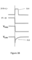
- 間隔を置かれた第1および第2の素子層と、ディスプレイピクセルの複数の行とを有する電気光学ディスプレイであって、ディスプレイピクセルの前記複数の行のうちの各1つの行は、
複数のディスプレイピクセルであって、前記複数のディスプレイピクセルの各々は、
前記第1の素子層に位置付けられたピクセル電極であって、前記ピクセル電極は、データラインを通じて供給される一連の電圧パルスで前記ディスプレイピクセルを駆動するために構成されている、ピクセル電極と、
前記第2の素子層に位置付けられたVCOM信号ラインであって、前記VCOM信号ラインは、前記ピクセル電極の一部分に重複している、VCOM信号ラインと、
ゲートラインと
を有し、前記ゲートラインは、前記V COM 信号ラインと平行である、複数のディスプレイピクセルと、
ディスプレイピクセルの前記1つの行のVCOM信号ラインを、ディスプレイピクセルの前記複数の行のうち、ディスプレイピクセルの前記1つの行に隣接する行のみのVCOM信号ラインのみに接続している導電路と
を備える、電気光学ディスプレイ。 - 前記導電路は、前記第2の素子層に位置付けられている、請求項1に記載の電気光学ディスプレイ。
- 電気光学媒質をさらに備えている、請求項1に記載の電気光学ディスプレイ。
- 前記電気光学媒質は、回転式二色部材または電気化学媒質である、請求項3に記載の電気光学ディスプレイ。
- 前記電気光学媒質は、電気泳動媒質であり、前記電気泳動媒質は、流体内の複数の荷電粒子を備え、前記複数の荷電粒子は、前記電気光学媒質への電場の印加時、前記流体を通って移動可能である、請求項3に記載の電気光学ディスプレイ。
- 前記V COM 信号ラインと平行な方向に前記導電路から間隔を置かれた第2の導電路をさらに備え、ディスプレイピクセルの前記複数の行は、ディスプレイピクセルの第1の行を含み、前記第2の導電路は、ディスプレイピクセルの前記第1の行の前記VCOM信号ラインをDC源のみに電気的に結合している、請求項1に記載の電気光学ディスプレイ。
- 前記複数のディスプレイピクセルの各々は、前記ピクセル電極と前記VCOM信号ラインとの間に形成された第1の静電容量をさらに備えている、請求項1に記載の電気光学ディスプレイ。
- 前記複数のディスプレイピクセルの各々は、前記データラインと前記VCOM信号ラインとの間に形成された第2の静電容量をさらに備えている、請求項7に記載の電気光学ディスプレイ。
Priority Applications (1)
| Application Number | Priority Date | Filing Date | Title |
|---|---|---|---|
| JP2022159462A JP2022173518A (ja) | 2018-11-09 | 2022-10-03 | 電気光学ディスプレイ |
Applications Claiming Priority (3)
| Application Number | Priority Date | Filing Date | Title |
|---|---|---|---|
| US201862757818P | 2018-11-09 | 2018-11-09 | |
| US62/757,818 | 2018-11-09 | ||
| PCT/US2019/060470 WO2020097462A1 (en) | 2018-11-09 | 2019-11-08 | Electro-optic displays |
Related Child Applications (1)
| Application Number | Title | Priority Date | Filing Date |
|---|---|---|---|
| JP2022159462A Division JP2022173518A (ja) | 2018-11-09 | 2022-10-03 | 電気光学ディスプレイ |
Publications (2)
| Publication Number | Publication Date |
|---|---|
| JP2022505740A JP2022505740A (ja) | 2022-01-14 |
| JP7250921B2 true JP7250921B2 (ja) | 2023-04-03 |
Family
ID=70551796
Family Applications (2)
| Application Number | Title | Priority Date | Filing Date |
|---|---|---|---|
| JP2021522394A Active JP7250921B2 (ja) | 2018-11-09 | 2019-11-08 | 電気光学ディスプレイ |
| JP2022159462A Withdrawn JP2022173518A (ja) | 2018-11-09 | 2022-10-03 | 電気光学ディスプレイ |
Family Applications After (1)
| Application Number | Title | Priority Date | Filing Date |
|---|---|---|---|
| JP2022159462A Withdrawn JP2022173518A (ja) | 2018-11-09 | 2022-10-03 | 電気光学ディスプレイ |
Country Status (7)
| Country | Link |
|---|---|
| US (2) | US11145262B2 (ja) |
| EP (1) | EP3877808A4 (ja) |
| JP (2) | JP7250921B2 (ja) |
| KR (2) | KR20230128588A (ja) |
| CN (1) | CN112955817A (ja) |
| TW (1) | TWI733246B (ja) |
| WO (1) | WO2020097462A1 (ja) |
Families Citing this family (1)
| Publication number | Priority date | Publication date | Assignee | Title |
|---|---|---|---|---|
| JP7250921B2 (ja) * | 2018-11-09 | 2023-04-03 | イー インク コーポレイション | 電気光学ディスプレイ |
Citations (5)
| Publication number | Priority date | Publication date | Assignee | Title |
|---|---|---|---|---|
| JP2003043948A (ja) | 2001-07-27 | 2003-02-14 | Sanyo Electric Co Ltd | アクティブマトリクス型表示装置 |
| JP2008233149A (ja) | 2007-03-16 | 2008-10-02 | Seiko Epson Corp | 電気光学装置及び電子機器、並びに電気光学装置の製造方法 |
| JP2011237788A (ja) | 2010-04-15 | 2011-11-24 | Semiconductor Energy Lab Co Ltd | 表示装置及びその駆動方法、並びに電子機器 |
| US20110298727A1 (en) | 2010-06-07 | 2011-12-08 | Marduke Yousefpor | Touch-display crosstalk |
| US20160018710A1 (en) | 2014-07-21 | 2016-01-21 | Li Chai | Display panel, array substrate and method for manufacturing the same |
Family Cites Families (173)
| Publication number | Priority date | Publication date | Assignee | Title |
|---|---|---|---|---|
| US3058659A (en) | 1958-12-31 | 1962-10-16 | Ibm | Add address to memory instruction |
| US3009344A (en) | 1959-12-31 | 1961-11-21 | Claude J Falconer | Diaper washer |
| US7259744B2 (en) | 1995-07-20 | 2007-08-21 | E Ink Corporation | Dielectrophoretic displays |
| US6866760B2 (en) | 1998-08-27 | 2005-03-15 | E Ink Corporation | Electrophoretic medium and process for the production thereof |
| US6639578B1 (en) | 1995-07-20 | 2003-10-28 | E Ink Corporation | Flexible displays |
| US7411719B2 (en) | 1995-07-20 | 2008-08-12 | E Ink Corporation | Electrophoretic medium and process for the production thereof |
| US7167155B1 (en) | 1995-07-20 | 2007-01-23 | E Ink Corporation | Color electrophoretic displays |
| US7106296B1 (en) | 1995-07-20 | 2006-09-12 | E Ink Corporation | Electronic book with multiple page displays |
| US7352353B2 (en) | 1995-07-20 | 2008-04-01 | E Ink Corporation | Electrostatically addressable electrophoretic display |
| US8089453B2 (en) | 1995-07-20 | 2012-01-03 | E Ink Corporation | Stylus-based addressing structures for displays |
| US6664944B1 (en) | 1995-07-20 | 2003-12-16 | E-Ink Corporation | Rear electrode structures for electrophoretic displays |
| US6120588A (en) | 1996-07-19 | 2000-09-19 | E Ink Corporation | Electronically addressable microencapsulated ink and display thereof |
| US7327511B2 (en) | 2004-03-23 | 2008-02-05 | E Ink Corporation | Light modulators |
| US6124851A (en) | 1995-07-20 | 2000-09-26 | E Ink Corporation | Electronic book with multiple page displays |
| EP0912913A1 (en) | 1996-07-19 | 1999-05-06 | E-Ink Corporation | Electronically addressable microencapsulated ink and display thereof |
| US5930026A (en) | 1996-10-25 | 1999-07-27 | Massachusetts Institute Of Technology | Nonemissive displays and piezoelectric power supplies therefor |
| US6980196B1 (en) | 1997-03-18 | 2005-12-27 | Massachusetts Institute Of Technology | Printable electronic display |
| US7002728B2 (en) | 1997-08-28 | 2006-02-21 | E Ink Corporation | Electrophoretic particles, and processes for the production thereof |
| US6252564B1 (en) | 1997-08-28 | 2001-06-26 | E Ink Corporation | Tiled displays |
| US6177921B1 (en) | 1997-08-28 | 2001-01-23 | E Ink Corporation | Printable electrode structures for displays |
| US6232950B1 (en) | 1997-08-28 | 2001-05-15 | E Ink Corporation | Rear electrode structures for displays |
| WO1999053371A1 (en) | 1998-04-10 | 1999-10-21 | E-Ink Corporation | Electronic displays using organic-based field effect transistors |
| US7075502B1 (en) | 1998-04-10 | 2006-07-11 | E Ink Corporation | Full color reflective display with multichromatic sub-pixels |
| US6241921B1 (en) | 1998-05-15 | 2001-06-05 | Massachusetts Institute Of Technology | Heterogeneous display elements and methods for their fabrication |
| WO1999067678A2 (en) | 1998-06-22 | 1999-12-29 | E-Ink Corporation | Means of addressing microencapsulated display media |
| EP1099207B1 (en) | 1998-07-22 | 2002-03-27 | E-Ink Corporation | Electronic display |
| USD485294S1 (en) | 1998-07-22 | 2004-01-13 | E Ink Corporation | Electrode structure for an electronic display |
| US7256766B2 (en) | 1998-08-27 | 2007-08-14 | E Ink Corporation | Electrophoretic display comprising optical biasing element |
| EP1118039B1 (en) | 1998-10-07 | 2003-02-05 | E Ink Corporation | Illumination system for nonemissive electronic displays |
| US6312304B1 (en) | 1998-12-15 | 2001-11-06 | E Ink Corporation | Assembly of microencapsulated electronic displays |
| US6506438B2 (en) | 1998-12-15 | 2003-01-14 | E Ink Corporation | Method for printing of transistor arrays on plastic substrates |
| US6724519B1 (en) | 1998-12-21 | 2004-04-20 | E-Ink Corporation | Protective electrodes for electrophoretic displays |
| AU2591400A (en) | 1998-12-22 | 2000-07-12 | E-Ink Corporation | Method of manufacturing of a discrete electronic device |
| TW521241B (en) | 1999-03-16 | 2003-02-21 | Sony Corp | Liquid crystal display apparatus, its driving method, and liquid crystal display system |
| US6842657B1 (en) | 1999-04-09 | 2005-01-11 | E Ink Corporation | Reactive formation of dielectric layers and protection of organic layers in organic semiconductor device fabrication |
| US6498114B1 (en) | 1999-04-09 | 2002-12-24 | E Ink Corporation | Method for forming a patterned semiconductor film |
| US7012600B2 (en) | 1999-04-30 | 2006-03-14 | E Ink Corporation | Methods for driving bistable electro-optic displays, and apparatus for use therein |
| US8009348B2 (en) | 1999-05-03 | 2011-08-30 | E Ink Corporation | Machine-readable displays |
| US7030412B1 (en) | 1999-05-05 | 2006-04-18 | E Ink Corporation | Minimally-patterned semiconductor devices for display applications |
| WO2001002899A2 (en) | 1999-07-01 | 2001-01-11 | E Ink Corporation | Electrophoretic medium provided with spacers |
| AU7137800A (en) | 1999-07-21 | 2001-02-13 | E-Ink Corporation | Preferred methods for producing electrical circuit elements used to control an electronic display |
| WO2001007961A1 (en) | 1999-07-21 | 2001-02-01 | E Ink Corporation | Use of a storage capacitor to enhance the performance of an active matrix driven electronic display |
| US6312971B1 (en) | 1999-08-31 | 2001-11-06 | E Ink Corporation | Solvent annealing process for forming a thin semiconductor film with advantageous properties |
| EP1208603A1 (en) | 1999-08-31 | 2002-05-29 | E Ink Corporation | Transistor for an electronically driven display |
| US6672921B1 (en) | 2000-03-03 | 2004-01-06 | Sipix Imaging, Inc. | Manufacturing process for electrophoretic display |
| US6788449B2 (en) | 2000-03-03 | 2004-09-07 | Sipix Imaging, Inc. | Electrophoretic display and novel process for its manufacture |
| US7715088B2 (en) | 2000-03-03 | 2010-05-11 | Sipix Imaging, Inc. | Electrophoretic display |
| EP1275156B1 (en) | 2000-04-18 | 2009-08-05 | E Ink Corporation | Process for fabricating thin film transistors |
| US7893435B2 (en) | 2000-04-18 | 2011-02-22 | E Ink Corporation | Flexible electronic circuits and displays including a backplane comprising a patterned metal foil having a plurality of apertures extending therethrough |
| US6683333B2 (en) | 2000-07-14 | 2004-01-27 | E Ink Corporation | Fabrication of electronic circuit elements using unpatterned semiconductor layers |
| US6816147B2 (en) | 2000-08-17 | 2004-11-09 | E Ink Corporation | Bistable electro-optic display, and method for addressing same |
| JP4198999B2 (ja) | 2001-03-13 | 2008-12-17 | イー インク コーポレイション | 図面を表示するための装置 |
| US7679814B2 (en) | 2001-04-02 | 2010-03-16 | E Ink Corporation | Materials for use in electrophoretic displays |
| CN1282027C (zh) | 2001-04-02 | 2006-10-25 | 伊英克公司 | 具有改善的图像稳定性的电泳介质 |
| US20020188053A1 (en) | 2001-06-04 | 2002-12-12 | Sipix Imaging, Inc. | Composition and process for the sealing of microcups in roll-to-roll display manufacturing |
| JP2004535599A (ja) | 2001-07-09 | 2004-11-25 | イー−インク コーポレイション | 電気光学ディスプレイおよび接着組成物 |
| US6982178B2 (en) | 2002-06-10 | 2006-01-03 | E Ink Corporation | Components and methods for use in electro-optic displays |
| US7535624B2 (en) | 2001-07-09 | 2009-05-19 | E Ink Corporation | Electro-optic display and materials for use therein |
| US7110163B2 (en) | 2001-07-09 | 2006-09-19 | E Ink Corporation | Electro-optic display and lamination adhesive for use therein |
| EP1415193B1 (en) | 2001-07-09 | 2012-03-14 | E Ink Corporation | Electro-optical display having a lamination adhesive layer |
| US6967640B2 (en) | 2001-07-27 | 2005-11-22 | E Ink Corporation | Microencapsulated electrophoretic display with integrated driver |
| US6819471B2 (en) | 2001-08-16 | 2004-11-16 | E Ink Corporation | Light modulation by frustration of total internal reflection |
| WO2003050607A1 (en) | 2001-12-13 | 2003-06-19 | E Ink Corporation | Electrophoretic electronic displays with films having a low index of refraction |
| US6885146B2 (en) * | 2002-03-14 | 2005-04-26 | Semiconductor Energy Laboratory Co., Ltd. | Display device comprising substrates, contrast medium and barrier layers between contrast medium and each of substrates |
| TWI240842B (en) | 2002-04-24 | 2005-10-01 | Sipix Imaging Inc | Matrix driven electrophoretic display with multilayer back plane |
| US7223672B2 (en) | 2002-04-24 | 2007-05-29 | E Ink Corporation | Processes for forming backplanes for electro-optic displays |
| US7190008B2 (en) | 2002-04-24 | 2007-03-13 | E Ink Corporation | Electro-optic displays, and components for use therein |
| TW574538B (en) | 2002-04-24 | 2004-02-01 | Sipix Imaging Inc | Compositions and processes for format flexible roll-to-roll manufacturing of electrophoretic displays |
| WO2003092077A2 (en) | 2002-04-24 | 2003-11-06 | E Ink Corporation | Electronic displays |
| TW583497B (en) | 2002-05-29 | 2004-04-11 | Sipix Imaging Inc | Electrode and connecting designs for roll-to-roll format flexible display manufacturing |
| US7583427B2 (en) | 2002-06-10 | 2009-09-01 | E Ink Corporation | Components and methods for use in electro-optic displays |
| US7649674B2 (en) | 2002-06-10 | 2010-01-19 | E Ink Corporation | Electro-optic display with edge seal |
| US8049947B2 (en) | 2002-06-10 | 2011-11-01 | E Ink Corporation | Components and methods for use in electro-optic displays |
| US7554712B2 (en) | 2005-06-23 | 2009-06-30 | E Ink Corporation | Edge seals for, and processes for assembly of, electro-optic displays |
| US6842279B2 (en) | 2002-06-27 | 2005-01-11 | E Ink Corporation | Illumination system for nonemissive electronic displays |
| US7347957B2 (en) | 2003-07-10 | 2008-03-25 | Sipix Imaging, Inc. | Methods and compositions for improved electrophoretic display performance |
| US8547628B2 (en) | 2002-07-17 | 2013-10-01 | Sipix Imaging, Inc. | Methods and compositions for improved electrophoretic display performance |
| TWI314237B (en) | 2002-07-17 | 2009-09-01 | Sipix Imaging Inc | Novel methods and compositions for improved electrophoretic display performance |
| US20060255322A1 (en) | 2002-07-17 | 2006-11-16 | Wu Zarng-Arh G | Methods and compositions for improved electrophoretic display performance |
| AU2003257197A1 (en) | 2002-08-06 | 2004-03-03 | E Ink Corporation | Protection of electro-optic displays against thermal effects |
| US7839564B2 (en) | 2002-09-03 | 2010-11-23 | E Ink Corporation | Components and methods for use in electro-optic displays |
| TW575646B (en) | 2002-09-04 | 2004-02-11 | Sipix Imaging Inc | Novel adhesive and sealing layers for electrophoretic displays |
| TWI229230B (en) | 2002-10-31 | 2005-03-11 | Sipix Imaging Inc | An improved electrophoretic display and novel process for its manufacture |
| US7365733B2 (en) | 2002-12-16 | 2008-04-29 | E Ink Corporation | Backplanes for electro-optic displays |
| US6922276B2 (en) | 2002-12-23 | 2005-07-26 | E Ink Corporation | Flexible electro-optic displays |
| ATE485535T1 (de) | 2003-03-27 | 2010-11-15 | E Ink Corp | Elektrooptische baugruppen |
| EP1631857B1 (en) | 2003-06-06 | 2007-03-07 | Sipix Imaging, Inc. | In mold manufacture of an object with embedded display panel |
| WO2005010598A2 (en) | 2003-07-24 | 2005-02-03 | E Ink Corporation | Electro-optic displays |
| WO2005024769A1 (en) | 2003-09-08 | 2005-03-17 | Koninklijke Philips Electronics, N.V. | Electrophoretic display activation with blanking frames |
| US8514168B2 (en) | 2003-10-07 | 2013-08-20 | Sipix Imaging, Inc. | Electrophoretic display with thermal control |
| US20050122306A1 (en) | 2003-10-29 | 2005-06-09 | E Ink Corporation | Electro-optic displays with single edge addressing and removable driver circuitry |
| US20110187683A1 (en) | 2003-10-30 | 2011-08-04 | E Ink Corporation | Electro-optic displays with single edge addressing and removable driver circuitry |
| US7672040B2 (en) | 2003-11-05 | 2010-03-02 | E Ink Corporation | Electro-optic displays, and materials for use therein |
| US8177942B2 (en) | 2003-11-05 | 2012-05-15 | E Ink Corporation | Electro-optic displays, and materials for use therein |
| US7551346B2 (en) | 2003-11-05 | 2009-06-23 | E Ink Corporation | Electro-optic displays, and materials for use therein |
| US20110164301A1 (en) | 2003-11-05 | 2011-07-07 | E Ink Corporation | Electro-optic displays, and materials for use therein |
| WO2005048228A2 (en) | 2003-11-05 | 2005-05-26 | E Ink Corporation | Electro-optic displays |
| US7206119B2 (en) | 2003-12-31 | 2007-04-17 | E Ink Corporation | Electro-optic displays, and method for driving same |
| US7075703B2 (en) | 2004-01-16 | 2006-07-11 | E Ink Corporation | Process for sealing electro-optic displays |
| US7388572B2 (en) | 2004-02-27 | 2008-06-17 | E Ink Corporation | Backplanes for electro-optic displays |
| US7453445B2 (en) | 2004-08-13 | 2008-11-18 | E Ink Corproation | Methods for driving electro-optic displays |
| US7301693B2 (en) | 2004-08-13 | 2007-11-27 | Sipix Imaging, Inc. | Direct drive display with a multi-layer backplane and process for its manufacture |
| US7304780B2 (en) | 2004-12-17 | 2007-12-04 | Sipix Imaging, Inc. | Backplane design for display panels and processes for their manufacture |
| JP2008521065A (ja) | 2005-01-26 | 2008-06-19 | イー インク コーポレイション | ガス状流体を用いる電気泳動ディスプレイ |
| US8576162B2 (en) | 2005-03-14 | 2013-11-05 | Sipix Imaging, Inc. | Manufacturing processes of backplane for segment displays |
| US8159636B2 (en) | 2005-04-08 | 2012-04-17 | Sipix Imaging, Inc. | Reflective displays and processes for their manufacture |
| US7880958B2 (en) | 2005-09-23 | 2011-02-01 | Sipix Imaging, Inc. | Display cell structure and electrode protecting layer compositions |
| US8610988B2 (en) | 2006-03-09 | 2013-12-17 | E Ink Corporation | Electro-optic display with edge seal |
| US20150005720A1 (en) | 2006-07-18 | 2015-01-01 | E Ink California, Llc | Electrophoretic display |
| US7492497B2 (en) | 2006-08-02 | 2009-02-17 | E Ink Corporation | Multi-layer light modulator |
| US8362488B2 (en) | 2006-09-12 | 2013-01-29 | Sipix Imaging, Inc. | Flexible backplane and methods for its manufacture |
| US7986450B2 (en) | 2006-09-22 | 2011-07-26 | E Ink Corporation | Electro-optic display and materials for use therein |
| US7905977B2 (en) | 2006-11-17 | 2011-03-15 | Sipix Imaging, Inc. | Post conversion methods for display devices |
| KR101362389B1 (ko) * | 2006-11-27 | 2014-02-12 | 삼성디스플레이 주식회사 | 전기영동 표시패널, 이를 구비한 전기영동 표시장치 및이의 구동 방법 |
| US8018428B2 (en) | 2006-11-27 | 2011-09-13 | Samsung Electronics Co., Ltd. | Electrophoretic display panel, electrophoretic display device having the same and method for driving the same |
| KR101361996B1 (ko) | 2006-12-23 | 2014-02-12 | 엘지디스플레이 주식회사 | 전기영동 표시장치와 그 구동방법 |
| US7688497B2 (en) | 2007-01-22 | 2010-03-30 | E Ink Corporation | Multi-layer sheet for use in electro-optic displays |
| EP2111562B1 (en) | 2007-01-22 | 2018-09-19 | E Ink Corporation | Multi-layer sheet for use in electro-optic displays |
| US7826129B2 (en) | 2007-03-06 | 2010-11-02 | E Ink Corporation | Materials for use in electrophoretic displays |
| JP2008293405A (ja) | 2007-05-28 | 2008-12-04 | Fuji Xerox Co Ltd | データ入力システム |
| US8034209B2 (en) | 2007-06-29 | 2011-10-11 | E Ink Corporation | Electro-optic displays, and materials and methods for production thereof |
| US8743077B1 (en) | 2007-08-01 | 2014-06-03 | Sipix Imaging, Inc. | Front light system for reflective displays |
| US20090122389A1 (en) | 2007-11-14 | 2009-05-14 | E Ink Corporation | Electro-optic assemblies, and adhesives and binders for use therein |
| US8237892B1 (en) | 2007-11-30 | 2012-08-07 | Sipix Imaging, Inc. | Display device with a brightness enhancement structure |
| US7830592B1 (en) | 2007-11-30 | 2010-11-09 | Sipix Imaging, Inc. | Display devices having micro-reflectors |
| WO2009114361A1 (en) | 2008-03-11 | 2009-09-17 | Sipix Imaging, Inc. | Luminance enhancement structure for reflective display devices |
| US8437069B2 (en) | 2008-03-11 | 2013-05-07 | Sipix Imaging, Inc. | Luminance enhancement structure for reflective display devices |
| US8072675B2 (en) | 2008-05-01 | 2011-12-06 | Sipix Imaging, Inc. | Color display devices |
| US8441414B2 (en) | 2008-12-05 | 2013-05-14 | Sipix Imaging, Inc. | Luminance enhancement structure with Moiré reducing design |
| KR101309364B1 (ko) * | 2008-12-24 | 2013-09-17 | 엘지디스플레이 주식회사 | 전기영동표시장치 및 그의 제조방법과 그의 리페어방법 |
| US8797258B2 (en) | 2008-12-30 | 2014-08-05 | Sipix Imaging, Inc. | Highlight color display architecture using enhanced dark state |
| US20100177396A1 (en) | 2009-01-13 | 2010-07-15 | Craig Lin | Asymmetrical luminance enhancement structure for reflective display devices |
| US20160077375A1 (en) | 2009-01-13 | 2016-03-17 | E Ink California, Llc | Asymmetrical luminance enhancement structure for reflective display devices |
| US9025234B2 (en) | 2009-01-22 | 2015-05-05 | E Ink California, Llc | Luminance enhancement structure with varying pitches |
| US8120836B2 (en) | 2009-03-09 | 2012-02-21 | Sipix Imaging, Inc. | Luminance enhancement structure for reflective display devices |
| US8714780B2 (en) | 2009-04-22 | 2014-05-06 | Sipix Imaging, Inc. | Display devices with grooved luminance enhancement film |
| US8797633B1 (en) | 2009-07-23 | 2014-08-05 | Sipix Imaging, Inc. | Display device assembly and manufacture thereof |
| US8456589B1 (en) | 2009-07-27 | 2013-06-04 | Sipix Imaging, Inc. | Display device assembly |
| US8614654B2 (en) * | 2009-07-30 | 2013-12-24 | Apple Inc. | Crosstalk reduction in LCD panels |
| US8754859B2 (en) | 2009-10-28 | 2014-06-17 | E Ink Corporation | Electro-optic displays with touch sensors and/or tactile feedback |
| US9620066B2 (en) | 2010-02-02 | 2017-04-11 | E Ink Corporation | Method for driving electro-optic displays |
| US9140952B2 (en) | 2010-04-22 | 2015-09-22 | E Ink California, Llc | Electrophoretic display with enhanced contrast |
| US9030374B2 (en) | 2010-05-06 | 2015-05-12 | E Ink California, Llc | Composite display modules |
| TW201207535A (en) | 2010-05-27 | 2012-02-16 | E Ink Corp | Dual mode electro-optic displays |
| WO2012063830A1 (ja) * | 2010-11-09 | 2012-05-18 | シャープ株式会社 | 液晶表示装置、表示装置およびゲート信号線駆動方法 |
| TW201235758A (en) * | 2011-02-24 | 2012-09-01 | Ind Tech Res Inst | Pixel structure, driving method and driving system of hybrid display device |
| TWI582509B (zh) | 2012-03-26 | 2017-05-11 | 達意科技股份有限公司 | 一種電泳式顯示面板及其結構 |
| US10190743B2 (en) | 2012-04-20 | 2019-01-29 | E Ink Corporation | Illumination systems for reflective displays |
| KR102022698B1 (ko) * | 2012-05-31 | 2019-11-05 | 삼성디스플레이 주식회사 | 표시 패널 |
| JP6178849B2 (ja) | 2012-06-20 | 2017-08-09 | イー・インク・カリフォルニア・リミテッド・ライアビリティ・カンパニーE Ink California,Llc | 圧電電気泳動表示装置 |
| US8797636B2 (en) | 2012-07-17 | 2014-08-05 | Sipix Imaging, Inc. | Light-enhancing structure for electrophoretic display |
| EP2877895B1 (en) | 2012-07-27 | 2017-09-06 | E Ink Corporation | Processes for the production of electro-optic displays |
| US9279906B2 (en) | 2012-08-31 | 2016-03-08 | E Ink California, Llc | Microstructure film |
| TWI478327B (zh) | 2012-11-01 | 2015-03-21 | Sipix Technology Inc | 顯示裝置 |
| US10037735B2 (en) | 2012-11-16 | 2018-07-31 | E Ink Corporation | Active matrix display with dual driving modes |
| TW201428569A (zh) | 2013-01-10 | 2014-07-16 | Sipix Technology Inc | 包含電泳觸控面板之顯示系統 |
| TWI502265B (zh) | 2013-01-25 | 2015-10-01 | Sipix Technology Inc | 電泳顯示器 |
| TWI502266B (zh) | 2013-02-20 | 2015-10-01 | Sipix Technology Inc | 降低被動式矩陣耦合效應的電泳顯示器 |
| US9666142B2 (en) | 2013-02-20 | 2017-05-30 | Sipix Technology, Inc. | Display capable of reducing passive matrix coupling effect |
| TWI502429B (zh) | 2013-06-13 | 2015-10-01 | Sipix Technology Inc | 觸控式顯示裝置及其製作方法 |
| TWI532599B (zh) | 2013-06-21 | 2016-05-11 | 達意科技股份有限公司 | 顯示面板以及顯示面板的製作方法 |
| US9223164B2 (en) | 2013-08-02 | 2015-12-29 | Sipix Technology, Inc. | Display |
| TWI502574B (zh) | 2013-10-09 | 2015-10-01 | Sipix Technology Inc | 光電裝置及其驅動方法 |
| KR102023860B1 (ko) | 2014-01-17 | 2019-09-20 | 이 잉크 코포레이션 | 2상의 전극층을 갖는 전기광학 디스플레이 |
| KR20160119195A (ko) * | 2014-02-07 | 2016-10-12 | 이 잉크 코포레이션 | 전기-광학 디스플레이 백플레인 구조들 |
| US10446585B2 (en) | 2014-03-17 | 2019-10-15 | E Ink Corporation | Multi-layer expanding electrode structures for backplane assemblies |
| US10444553B2 (en) | 2014-03-25 | 2019-10-15 | E Ink California, Llc | Magnetophoretic display assembly and driving scheme |
| CN104020881B (zh) | 2014-05-29 | 2017-06-16 | 京东方科技集团股份有限公司 | 触摸显示面板及其驱动方法、显示装置 |
| TWI613498B (zh) | 2014-06-27 | 2018-02-01 | 電子墨水加利福尼亞有限責任公司 | 用於電泳顯示器的各向異性傳導介電層 |
| US20160012710A1 (en) | 2014-07-10 | 2016-01-14 | Sipix Technology Inc. | Smart medication device |
| CN104280969A (zh) * | 2014-11-03 | 2015-01-14 | 友达光电股份有限公司 | 一种液晶面板及其制造方法 |
| TWI579628B (zh) * | 2015-01-05 | 2017-04-21 | 電子墨水股份有限公司 | 光電顯示器及用於驅動光電顯示器之方法 |
| JP7250921B2 (ja) * | 2018-11-09 | 2023-04-03 | イー インク コーポレイション | 電気光学ディスプレイ |
-
2019
- 2019-11-08 JP JP2021522394A patent/JP7250921B2/ja active Active
- 2019-11-08 US US16/678,323 patent/US11145262B2/en active Active
- 2019-11-08 CN CN201980070491.8A patent/CN112955817A/zh active Pending
- 2019-11-08 WO PCT/US2019/060470 patent/WO2020097462A1/en unknown
- 2019-11-08 TW TW108140715A patent/TWI733246B/zh active
- 2019-11-08 KR KR1020237029211A patent/KR20230128588A/ko not_active Application Discontinuation
- 2019-11-08 KR KR1020217016478A patent/KR102576895B1/ko active IP Right Grant
- 2019-11-08 EP EP19882567.1A patent/EP3877808A4/en active Pending
-
2021
- 2021-10-07 US US17/496,749 patent/US11450287B2/en active Active
-
2022
- 2022-10-03 JP JP2022159462A patent/JP2022173518A/ja not_active Withdrawn
Patent Citations (5)
| Publication number | Priority date | Publication date | Assignee | Title |
|---|---|---|---|---|
| JP2003043948A (ja) | 2001-07-27 | 2003-02-14 | Sanyo Electric Co Ltd | アクティブマトリクス型表示装置 |
| JP2008233149A (ja) | 2007-03-16 | 2008-10-02 | Seiko Epson Corp | 電気光学装置及び電子機器、並びに電気光学装置の製造方法 |
| JP2011237788A (ja) | 2010-04-15 | 2011-11-24 | Semiconductor Energy Lab Co Ltd | 表示装置及びその駆動方法、並びに電子機器 |
| US20110298727A1 (en) | 2010-06-07 | 2011-12-08 | Marduke Yousefpor | Touch-display crosstalk |
| US20160018710A1 (en) | 2014-07-21 | 2016-01-21 | Li Chai | Display panel, array substrate and method for manufacturing the same |
Also Published As
| Publication number | Publication date |
|---|---|
| EP3877808A4 (en) | 2022-07-27 |
| KR102576895B1 (ko) | 2023-09-08 |
| TWI733246B (zh) | 2021-07-11 |
| US20220028347A1 (en) | 2022-01-27 |
| JP2022173518A (ja) | 2022-11-18 |
| JP2022505740A (ja) | 2022-01-14 |
| US11450287B2 (en) | 2022-09-20 |
| KR20230128588A (ko) | 2023-09-05 |
| TW202103133A (zh) | 2021-01-16 |
| US11145262B2 (en) | 2021-10-12 |
| EP3877808A1 (en) | 2021-09-15 |
| CN112955817A (zh) | 2021-06-11 |
| KR20210068596A (ko) | 2021-06-09 |
| WO2020097462A1 (en) | 2020-05-14 |
| US20200152140A1 (en) | 2020-05-14 |
Similar Documents
| Publication | Publication Date | Title |
|---|---|---|
| US20230089428A1 (en) | Electro-optic displays | |
| TWI728631B (zh) | 電光顯示器 | |
| JP2022173518A (ja) | 電気光学ディスプレイ | |
| US20220398956A1 (en) | Methods and apparatuses for driving electro-optic displays | |
| JP2019518249A (ja) | 電気光学ディスプレイのためのバックプレーン | |
| US20180102081A1 (en) | Driving methods for electro-optic displays | |
| RU2783032C1 (ru) | Электрооптические дисплеи | |
| CN118033960A (en) | Electro-optic display |
Legal Events
| Date | Code | Title | Description |
|---|---|---|---|
| A621 | Written request for application examination |
Free format text: JAPANESE INTERMEDIATE CODE: A621 Effective date: 20210423 |
|
| A977 | Report on retrieval |
Free format text: JAPANESE INTERMEDIATE CODE: A971007 Effective date: 20220428 |
|
| A131 | Notification of reasons for refusal |
Free format text: JAPANESE INTERMEDIATE CODE: A131 Effective date: 20220502 |
|
| A601 | Written request for extension of time |
Free format text: JAPANESE INTERMEDIATE CODE: A601 Effective date: 20220801 |
|
| A521 | Request for written amendment filed |
Free format text: JAPANESE INTERMEDIATE CODE: A523 Effective date: 20221003 |
|
| A131 | Notification of reasons for refusal |
Free format text: JAPANESE INTERMEDIATE CODE: A131 Effective date: 20221024 |
|
| A521 | Request for written amendment filed |
Free format text: JAPANESE INTERMEDIATE CODE: A523 Effective date: 20230124 |
|
| TRDD | Decision of grant or rejection written | ||
| A01 | Written decision to grant a patent or to grant a registration (utility model) |
Free format text: JAPANESE INTERMEDIATE CODE: A01 Effective date: 20230228 |
|
| A61 | First payment of annual fees (during grant procedure) |
Free format text: JAPANESE INTERMEDIATE CODE: A61 Effective date: 20230322 |
|
| R150 | Certificate of patent or registration of utility model |
Ref document number: 7250921 Country of ref document: JP Free format text: JAPANESE INTERMEDIATE CODE: R150 |