JP7203526B2 - Organic electroluminescent materials and devices - Google Patents
Organic electroluminescent materials and devices Download PDFInfo
- Publication number
- JP7203526B2 JP7203526B2 JP2018138172A JP2018138172A JP7203526B2 JP 7203526 B2 JP7203526 B2 JP 7203526B2 JP 2018138172 A JP2018138172 A JP 2018138172A JP 2018138172 A JP2018138172 A JP 2018138172A JP 7203526 B2 JP7203526 B2 JP 7203526B2
- Authority
- JP
- Japan
- Prior art keywords
- host
- energy
- emitter
- homo
- oled
- Prior art date
- Legal status (The legal status is an assumption and is not a legal conclusion. Google has not performed a legal analysis and makes no representation as to the accuracy of the status listed.)
- Active
Links
Images


Classifications
-
- C—CHEMISTRY; METALLURGY
- C07—ORGANIC CHEMISTRY
- C07F—ACYCLIC, CARBOCYCLIC OR HETEROCYCLIC COMPOUNDS CONTAINING ELEMENTS OTHER THAN CARBON, HYDROGEN, HALOGEN, OXYGEN, NITROGEN, SULFUR, SELENIUM OR TELLURIUM
- C07F15/00—Compounds containing elements of Groups 8, 9, 10 or 18 of the Periodic System
- C07F15/0006—Compounds containing elements of Groups 8, 9, 10 or 18 of the Periodic System compounds of the platinum group
- C07F15/0033—Iridium compounds
-
- H—ELECTRICITY
- H10—SEMICONDUCTOR DEVICES; ELECTRIC SOLID-STATE DEVICES NOT OTHERWISE PROVIDED FOR
- H10K—ORGANIC ELECTRIC SOLID-STATE DEVICES
- H10K85/00—Organic materials used in the body or electrodes of devices covered by this subclass
- H10K85/30—Coordination compounds
- H10K85/341—Transition metal complexes, e.g. Ru(II)polypyridine complexes
- H10K85/342—Transition metal complexes, e.g. Ru(II)polypyridine complexes comprising iridium
-
- C—CHEMISTRY; METALLURGY
- C07—ORGANIC CHEMISTRY
- C07F—ACYCLIC, CARBOCYCLIC OR HETEROCYCLIC COMPOUNDS CONTAINING ELEMENTS OTHER THAN CARBON, HYDROGEN, HALOGEN, OXYGEN, NITROGEN, SULFUR, SELENIUM OR TELLURIUM
- C07F15/00—Compounds containing elements of Groups 8, 9, 10 or 18 of the Periodic System
- C07F15/0006—Compounds containing elements of Groups 8, 9, 10 or 18 of the Periodic System compounds of the platinum group
- C07F15/0086—Platinum compounds
-
- C—CHEMISTRY; METALLURGY
- C09—DYES; PAINTS; POLISHES; NATURAL RESINS; ADHESIVES; COMPOSITIONS NOT OTHERWISE PROVIDED FOR; APPLICATIONS OF MATERIALS NOT OTHERWISE PROVIDED FOR
- C09K—MATERIALS FOR MISCELLANEOUS APPLICATIONS, NOT PROVIDED FOR ELSEWHERE
- C09K11/00—Luminescent, e.g. electroluminescent, chemiluminescent materials
- C09K11/06—Luminescent, e.g. electroluminescent, chemiluminescent materials containing organic luminescent materials
-
- H—ELECTRICITY
- H10—SEMICONDUCTOR DEVICES; ELECTRIC SOLID-STATE DEVICES NOT OTHERWISE PROVIDED FOR
- H10K—ORGANIC ELECTRIC SOLID-STATE DEVICES
- H10K50/00—Organic light-emitting devices
- H10K50/10—OLEDs or polymer light-emitting diodes [PLED]
- H10K50/11—OLEDs or polymer light-emitting diodes [PLED] characterised by the electroluminescent [EL] layers
- H10K50/12—OLEDs or polymer light-emitting diodes [PLED] characterised by the electroluminescent [EL] layers comprising dopants
-
- H—ELECTRICITY
- H10—SEMICONDUCTOR DEVICES; ELECTRIC SOLID-STATE DEVICES NOT OTHERWISE PROVIDED FOR
- H10K—ORGANIC ELECTRIC SOLID-STATE DEVICES
- H10K50/00—Organic light-emitting devices
- H10K50/10—OLEDs or polymer light-emitting diodes [PLED]
- H10K50/18—Carrier blocking layers
-
- H—ELECTRICITY
- H10—SEMICONDUCTOR DEVICES; ELECTRIC SOLID-STATE DEVICES NOT OTHERWISE PROVIDED FOR
- H10K—ORGANIC ELECTRIC SOLID-STATE DEVICES
- H10K50/00—Organic light-emitting devices
- H10K50/80—Constructional details
- H10K50/805—Electrodes
- H10K50/81—Anodes
-
- H—ELECTRICITY
- H10—SEMICONDUCTOR DEVICES; ELECTRIC SOLID-STATE DEVICES NOT OTHERWISE PROVIDED FOR
- H10K—ORGANIC ELECTRIC SOLID-STATE DEVICES
- H10K50/00—Organic light-emitting devices
- H10K50/80—Constructional details
- H10K50/805—Electrodes
- H10K50/82—Cathodes
-
- H—ELECTRICITY
- H10—SEMICONDUCTOR DEVICES; ELECTRIC SOLID-STATE DEVICES NOT OTHERWISE PROVIDED FOR
- H10K—ORGANIC ELECTRIC SOLID-STATE DEVICES
- H10K85/00—Organic materials used in the body or electrodes of devices covered by this subclass
- H10K85/30—Coordination compounds
- H10K85/341—Transition metal complexes, e.g. Ru(II)polypyridine complexes
- H10K85/346—Transition metal complexes, e.g. Ru(II)polypyridine complexes comprising platinum
-
- H—ELECTRICITY
- H10—SEMICONDUCTOR DEVICES; ELECTRIC SOLID-STATE DEVICES NOT OTHERWISE PROVIDED FOR
- H10K—ORGANIC ELECTRIC SOLID-STATE DEVICES
- H10K85/00—Organic materials used in the body or electrodes of devices covered by this subclass
- H10K85/60—Organic compounds having low molecular weight
- H10K85/649—Aromatic compounds comprising a hetero atom
- H10K85/657—Polycyclic condensed heteroaromatic hydrocarbons
- H10K85/6572—Polycyclic condensed heteroaromatic hydrocarbons comprising only nitrogen in the heteroaromatic polycondensed ring system, e.g. phenanthroline or carbazole
-
- H—ELECTRICITY
- H10—SEMICONDUCTOR DEVICES; ELECTRIC SOLID-STATE DEVICES NOT OTHERWISE PROVIDED FOR
- H10K—ORGANIC ELECTRIC SOLID-STATE DEVICES
- H10K85/00—Organic materials used in the body or electrodes of devices covered by this subclass
- H10K85/60—Organic compounds having low molecular weight
- H10K85/649—Aromatic compounds comprising a hetero atom
- H10K85/657—Polycyclic condensed heteroaromatic hydrocarbons
- H10K85/6576—Polycyclic condensed heteroaromatic hydrocarbons comprising only sulfur in the heteroaromatic polycondensed ring system, e.g. benzothiophene
-
- C—CHEMISTRY; METALLURGY
- C09—DYES; PAINTS; POLISHES; NATURAL RESINS; ADHESIVES; COMPOSITIONS NOT OTHERWISE PROVIDED FOR; APPLICATIONS OF MATERIALS NOT OTHERWISE PROVIDED FOR
- C09K—MATERIALS FOR MISCELLANEOUS APPLICATIONS, NOT PROVIDED FOR ELSEWHERE
- C09K2211/00—Chemical nature of organic luminescent or tenebrescent compounds
- C09K2211/18—Metal complexes
- C09K2211/185—Metal complexes of the platinum group, i.e. Os, Ir, Pt, Ru, Rh or Pd
-
- H—ELECTRICITY
- H10—SEMICONDUCTOR DEVICES; ELECTRIC SOLID-STATE DEVICES NOT OTHERWISE PROVIDED FOR
- H10K—ORGANIC ELECTRIC SOLID-STATE DEVICES
- H10K2101/00—Properties of the organic materials covered by group H10K85/00
- H10K2101/10—Triplet emission
-
- H—ELECTRICITY
- H10—SEMICONDUCTOR DEVICES; ELECTRIC SOLID-STATE DEVICES NOT OTHERWISE PROVIDED FOR
- H10K—ORGANIC ELECTRIC SOLID-STATE DEVICES
- H10K2101/00—Properties of the organic materials covered by group H10K85/00
- H10K2101/40—Interrelation of parameters between multiple constituent active layers or sublayers, e.g. HOMO values in adjacent layers
-
- H—ELECTRICITY
- H10—SEMICONDUCTOR DEVICES; ELECTRIC SOLID-STATE DEVICES NOT OTHERWISE PROVIDED FOR
- H10K—ORGANIC ELECTRIC SOLID-STATE DEVICES
- H10K2101/00—Properties of the organic materials covered by group H10K85/00
- H10K2101/90—Multiple hosts in the emissive layer
-
- H—ELECTRICITY
- H10—SEMICONDUCTOR DEVICES; ELECTRIC SOLID-STATE DEVICES NOT OTHERWISE PROVIDED FOR
- H10K—ORGANIC ELECTRIC SOLID-STATE DEVICES
- H10K50/00—Organic light-emitting devices
- H10K50/10—OLEDs or polymer light-emitting diodes [PLED]
- H10K50/14—Carrier transporting layers
- H10K50/15—Hole transporting layers
-
- H—ELECTRICITY
- H10—SEMICONDUCTOR DEVICES; ELECTRIC SOLID-STATE DEVICES NOT OTHERWISE PROVIDED FOR
- H10K—ORGANIC ELECTRIC SOLID-STATE DEVICES
- H10K50/00—Organic light-emitting devices
- H10K50/10—OLEDs or polymer light-emitting diodes [PLED]
- H10K50/14—Carrier transporting layers
- H10K50/16—Electron transporting layers
-
- H—ELECTRICITY
- H10—SEMICONDUCTOR DEVICES; ELECTRIC SOLID-STATE DEVICES NOT OTHERWISE PROVIDED FOR
- H10K—ORGANIC ELECTRIC SOLID-STATE DEVICES
- H10K85/00—Organic materials used in the body or electrodes of devices covered by this subclass
- H10K85/40—Organosilicon compounds, e.g. TIPS pentacene
-
- H—ELECTRICITY
- H10—SEMICONDUCTOR DEVICES; ELECTRIC SOLID-STATE DEVICES NOT OTHERWISE PROVIDED FOR
- H10K—ORGANIC ELECTRIC SOLID-STATE DEVICES
- H10K85/00—Organic materials used in the body or electrodes of devices covered by this subclass
- H10K85/60—Organic compounds having low molecular weight
- H10K85/615—Polycyclic condensed aromatic hydrocarbons, e.g. anthracene
- H10K85/626—Polycyclic condensed aromatic hydrocarbons, e.g. anthracene containing more than one polycyclic condensed aromatic rings, e.g. bis-anthracene
-
- H—ELECTRICITY
- H10—SEMICONDUCTOR DEVICES; ELECTRIC SOLID-STATE DEVICES NOT OTHERWISE PROVIDED FOR
- H10K—ORGANIC ELECTRIC SOLID-STATE DEVICES
- H10K85/00—Organic materials used in the body or electrodes of devices covered by this subclass
- H10K85/60—Organic compounds having low molecular weight
- H10K85/649—Aromatic compounds comprising a hetero atom
- H10K85/657—Polycyclic condensed heteroaromatic hydrocarbons
-
- Y—GENERAL TAGGING OF NEW TECHNOLOGICAL DEVELOPMENTS; GENERAL TAGGING OF CROSS-SECTIONAL TECHNOLOGIES SPANNING OVER SEVERAL SECTIONS OF THE IPC; TECHNICAL SUBJECTS COVERED BY FORMER USPC CROSS-REFERENCE ART COLLECTIONS [XRACs] AND DIGESTS
- Y02—TECHNOLOGIES OR APPLICATIONS FOR MITIGATION OR ADAPTATION AGAINST CLIMATE CHANGE
- Y02E—REDUCTION OF GREENHOUSE GAS [GHG] EMISSIONS, RELATED TO ENERGY GENERATION, TRANSMISSION OR DISTRIBUTION
- Y02E10/00—Energy generation through renewable energy sources
- Y02E10/50—Photovoltaic [PV] energy
- Y02E10/549—Organic PV cells
Description
関連出願の相互参照
本願は、その内容の全体を参照によって援用する、2017年7月26日出願の米国仮出願第62/537,029号の優先権を主張する非仮出願である。
CROSS-REFERENCE TO RELATED APPLICATIONS This application is a non-provisional application claiming priority to US Provisional Application No. 62/537,029, filed July 26, 2017, the entire contents of which are incorporated by reference.
本発明は、特定のエネルギー準位を有する電子輸送ホスト及び/又は正孔輸送ホストを用いて青色スペクトル領域の光を発する有機発光デバイスのための新規なデバイス構造に関する。 The present invention relates to novel device structures for organic light-emitting devices that emit light in the blue spectral region using electron-transporting hosts and/or hole-transporting hosts with specific energy levels.
有機材料を利用する光電子デバイスは、いくつもの理由から、次第に望ましいものとなりつつある。そのようなデバイスを作製するために使用される材料の多くは比較的安価であるため、有機光電子デバイスは無機デバイスを上回るコスト優位性の可能性を有する。加えて、柔軟性等の有機材料の固有の特性により、該材料は、フレキシブル基板上での製作等の特定用途によく適したものとなり得る。有機光電子デバイスの例は、有機発光ダイオード/デバイス(OLED)、有機光トランジスタ、有機光電池及び有機光検出器を含む。OLEDについて、有機材料は従来の材料を上回る性能の利点を有し得る。例えば、有機発光層が光を放出する波長は、概して、適切なドーパントで容易に調整され得る。 Optoelectronic devices utilizing organic materials are becoming increasingly desirable for a number of reasons. Organic optoelectronic devices have a potential cost advantage over inorganic devices because many of the materials used to make such devices are relatively inexpensive. In addition, the inherent properties of organic materials, such as flexibility, can make them well suited for certain applications, such as fabrication on flexible substrates. Examples of organic optoelectronic devices include organic light emitting diodes/devices (OLEDs), organic phototransistors, organic photovoltaic cells and organic photodetectors. For OLEDs, organic materials can have performance advantages over conventional materials. For example, the wavelength at which an organic light-emitting layer emits light can generally be easily tuned with appropriate dopants.
OLEDはデバイス全体に電圧が印加されると光を放出する薄い有機膜を利用する。OLEDは、フラットパネルディスプレイ、照明及びバックライティング等の用途において使用するためのますます興味深い技術となりつつある。数種のOLED材料及び構成は、参照によりその全体が本明細書に組み込まれる、特許文献1、特許文献2及び特許文献3において記述されている。 OLEDs utilize thin organic films that emit light when a voltage is applied across the device. OLEDs are becoming an increasingly interesting technology for use in applications such as flat panel displays, lighting and backlighting. Several OLED materials and configurations are described in US Pat.
リン光性発光分子の1つの用途は、フルカラーディスプレイである。そのようなディスプレイの業界標準は、「飽和(saturated)」色と称される特定の色を放出するように適合された画素を必要とする。特に、これらの標準は、飽和した赤色、緑色及び青色画素を必要とする。若しくは、OLEDは、白色光を照射するように設計することができる。従来の、白色バックライトからの液晶ディスプレイ発光は、吸収フィルターを用いてフィルタリングされ、赤色、緑色、及び青色発光を生成する。同様の技術は、OLEDでも用いられることができる。白色OLEDは、単一のEMLデバイス又は積層体構造のいずれかであることができる。色は、当技術分野において周知のCIE座標を使用して測定することができる。 One application of phosphorescent emissive molecules is in full color displays. Industry standards for such displays require pixels adapted to emit a particular color, referred to as a "saturated" color. In particular, these standards require saturated red, green and blue pixels. Alternatively, the OLED can be designed to emit white light. Liquid crystal display emissions from a conventional white backlight are filtered using absorptive filters to produce red, green, and blue emissions. Similar techniques can also be used with OLEDs. White OLEDs can be either single EML devices or stacked structures. Color can be measured using CIE coordinates, which are well known in the art.
緑色発光分子の一例は、下記の構造:

この図面及び本明細書における後出の図面中で、本発明者らは、窒素から金属(ここではIr)への配位結合を直線として描写する。 In this figure and later figures in this specification, we depict the coordinate bonds from nitrogen to metal (here Ir) as straight lines.
本明細書において使用される場合、用語「有機」は、有機光電子デバイスを製作するために使用され得るポリマー材料及び小分子有機材料を含む。「小分子」は、ポリマーでない任意の有機材料を指し、且つ「小分子」は実際にはかなり大型であってよい。小分子は、いくつかの状況において繰り返し単位を含み得る。例えば、長鎖アルキル基を置換基として使用することは、「小分子」クラスから分子を排除しない。小分子は、例えばポリマー骨格上のペンダント基として、又は該骨格の一部として、ポリマーに組み込まれてもよい。小分子は、コア部分上に構築された一連の化学的シェルからなるデンドリマーのコア部分として役立つこともできる。デンドリマーのコア部分は、蛍光性又はリン光性小分子発光体であってよい。デンドリマーは「小分子」であってよく、OLEDの分野において現在使用されているデンドリマーはすべて小分子であると考えられている。 As used herein, the term "organic" includes polymeric materials and small molecule organic materials that can be used to fabricate organic optoelectronic devices. "Small molecule" refers to any organic material that is not a polymer, and "small molecule" may actually be quite large. Small molecules may include repeat units in some situations. For example, using a long chain alkyl group as a substituent does not eliminate a molecule from the "small molecule" class. Small molecules may be incorporated into polymers, for example, as pendant groups on the polymer backbone or as part of the backbone. Small molecules can also serve as the core portion of a dendrimer, which consists of a series of chemical shells built on the core portion. The core portion of the dendrimer can be a fluorescent or phosphorescent small molecule emitter. A dendrimer may be a "small molecule" and it is believed that all dendrimers currently used in the OLED field are small molecules.
本明細書において使用される場合、「頂部」は基板から最遠部を意味するのに対し、「底部」は基板の最近部を意味する。第一層が第二層「の上に配置されている」と記述される場合、第一層のほうが基板から遠くに配置されている。第一層が第二層「と接触している」ことが指定されているのでない限り、第一層と第二層との間に他の層があってもよい。例えば、間に種々の有機層があるとしても、カソードはアノード「の上に配置されている」と記述され得る。 As used herein, "top" means furthest from the substrate, while "bottom" means nearest to the substrate. When a first layer is described as being "disposed over" a second layer, the first layer is positioned further from the substrate. There may be other layers between the first and second layers, unless it is specified that the first layer is "in contact with" the second layer. For example, a cathode may be described as being "disposed over" an anode, even though there are various organic layers in between.
本明細書において使用される場合、「溶液プロセス可能な」は、溶液又は懸濁液形態のいずれかの液体媒質に溶解、分散若しくは輸送することができ、且つ/又は該媒質から堆積することができるという意味である。 As used herein, "solution processable" is capable of being dissolved, dispersed or transported in and/or deposited from a liquid medium, either in solution or suspension form. It means you can.
配位子は、該配位子が発光材料の光活性特性に直接寄与していると考えられる場合、「光活性」と称され得る。配位子は、該配位子が発光材料の光活性特性に寄与していないと考えられる場合には「補助」と称され得るが、補助配位子は、光活性配位子の特性を変化させることができる。 A ligand may be referred to as "photoactive" if it is believed that the ligand directly contributes to the photoactive properties of the emissive material. A ligand may be referred to as an "ancillary" ligand when it is believed that the ligand does not contribute to the photoactive properties of the emissive material; can be changed.
本明細書において使用される場合、当業者には概して理解されるであろう通り、第一の「最高被占分子軌道」(HOMO)又は「最低空分子軌道」(LUMO)エネルギー準位は、第一のエネルギー準位が真空エネルギー準位に近ければ、第二のHOMO又はLUMOエネルギー準位「よりも大きい」又は「よりも高い」。イオン化ポテンシャル(IP)は、真空準位と比べて負のエネルギーとして測定されるため、より高いHOMOエネルギー準位は、より小さい絶対値を有するIP(あまり負でないIP)に相当する。同様に、より高いLUMOエネルギー準位は、より小さい絶対値を有する電子親和力(EA)(あまり負でないEA)に相当する。頂部に真空準位がある従来のエネルギー準位図において、材料のLUMOエネルギー準位は、同じ材料のHOMOエネルギー準位よりも高い。「より高い」HOMO又はLUMOエネルギー準位は、「より低い」HOMO又はLUMOエネルギー準位よりもそのような図の頂部に近いように思われる。 As used herein, as will be generally understood by those skilled in the art, the first "highest occupied molecular orbital" (HOMO) or "lowest unoccupied molecular orbital" (LUMO) energy level is A second HOMO or LUMO energy level is “greater than” or “higher than” if the first energy level is close to the vacuum energy level. Since the ionization potential (IP) is measured as negative energy compared to the vacuum level, a higher HOMO energy level corresponds to an IP with a smaller absolute value (less negative IP). Similarly, higher LUMO energy levels correspond to electron affinities (EAs) with smaller absolute values (less negative EAs). In a conventional energy level diagram with the vacuum level on top, the LUMO energy level of a material is higher than the HOMO energy level of the same material. A "higher" HOMO or LUMO energy level appears closer to the top of such a diagram than a "lower" HOMO or LUMO energy level.
本明細書において使用される場合、当業者には概して理解されるであろう通り、第一の仕事関数がより高い絶対値を有するならば、第一の仕事関数は第二の仕事関数「よりも大きい」又は「よりも高い」。仕事関数は概して真空準位と比べて負数として測定されるため、これは「より高い」仕事関数が更に負であることを意味する。頂部に真空準位がある従来のエネルギー準位図において、「より高い」仕事関数は、真空準位から下向きの方向に遠く離れているものとして例証される。故に、HOMO及びLUMOエネルギー準位の定義は、仕事関数とは異なる慣例に準ずる。 As used herein, as will be generally understood by those of ordinary skill in the art, a first work function is "more greater than” or “higher than”. Since work functions are generally measured as negative numbers relative to the vacuum level, this means that a "higher" work function is more negative. In a conventional energy level diagram with the vacuum level at the top, the "higher" work function is illustrated as farther away from the vacuum level in the downward direction. Therefore, the definition of HOMO and LUMO energy levels follows a different convention than work function.
OLEDについての更なる詳細及び上述した定義は、参照によりその全体が本明細書に組み込まれる特許文献4において見ることができる。 Further details about OLEDs and the definitions given above can be found in US Pat.
商業的な高性能青色発光デバイス、即ち、青色(発光スペクトルの最大波長が約500nm未満)を発するデバイス(以下、「青色デバイス」と称する)を高効率且つ長デバイス寿命で達成するために、OLED産業は、大きな課題を持ち続けている。過去においては、青色発光デバイスは、その発光層に、主に、広いバンドギャップホスト材料又は正孔輸送ホスト材料を使用した。本開示において、発明者らは、特定のエネルギー要件を有する電子輸送ホスト(e-ホスト)材料及び/又は正孔輸送ホスト(h-ホスト)材料を利用する新規デバイスを開示する。これらの新しいデバイスは、全体的なデバイス性能を著しく改善することができる。 In order to achieve commercial high-performance blue light-emitting devices, i.e., devices that emit blue (the maximum wavelength of the emission spectrum is less than about 500 nm) (hereinafter referred to as "blue devices") with high efficiency and long device lifetime, OLEDs The industry continues to face major challenges. In the past, blue light-emitting devices have primarily used wide bandgap or hole-transporting host materials in their light-emitting layers. In this disclosure, we disclose novel devices that utilize electron-transporting host (e-host) and/or hole-transporting host (h-host) materials with specific energy requirements. These new devices can significantly improve overall device performance.
OLEDが開示され、前記OLEDは、アノードと、カソードと、前記アノードと前記カソードとの間に配された有機発光層とを含む。前記有機発光層は、第1のホストと発光体とを含む。前記第1のホストと前記発光体はそれぞれ、HOMOエネルギー、LUMOエネルギー、及びT1三重項エネルギーを有する材料のものである。前記発光体は、リン光金属錯体及び遅延蛍光発光体からなる群から選択される。前記第1のホストのT1三重項エネルギーであるEH1Tは、前記発光体のT1三重項エネルギーであるEETよりも高く、EETは、少なくとも2.50eVである。前記第1のホストのLUMOエネルギー準位は、前記発光体のHOMOエネルギー準位よりも高い。前記発光体のHOMOエネルギーと前記第1のホストのLUMOエネルギーとの間の差の絶対値は、ΔE1で表され、a≦ΔE1-EET≦bであり、a≧0.005eV且つb≦0.60eVである。 An OLED is disclosed that includes an anode, a cathode, and an organic light emitting layer disposed between the anode and the cathode. The organic light emitting layer includes a first host and a light emitter. The first host and the emitter are of materials having HOMO energy, LUMO energy and T1 triplet energy, respectively . The emitter is selected from the group consisting of phosphorescent metal complexes and delayed fluorescence emitters. The T1 triplet energy of the first host, EH1T , is higher than the T1 triplet energy of the emitter, EET, and EET is at least 2.50 eV. The LUMO energy level of the first host is higher than the HOMO energy level of the emitter. The absolute value of the difference between the HOMO energy of the emitter and the LUMO energy of the first host is denoted by ΔE1, a≦ΔE1−E ET ≦b, a≧0.005 eV and b≦0. .60 eV.
幾つかの実施形態においては、OLEDが開示され、前記OLEDは、アノードと、カソードと、前記アノードと前記カソードとの間に配された有機発光層とを含む。前記有機発光層は、第1のホストと、第2のホストと、発光体とを含む。前記第1のホスト、前記第2のホスト、及び前記発光体はそれぞれ、HOMOエネルギー、LUMOエネルギー、及びT1三重項エネルギーを有する材料のものである。前記発光体は、リン光金属錯体及び遅延蛍光発光体からなる群から選択される。前記第1のホストのT1三重項エネルギーであるEH1Tが、前記発光体のT1三重項エネルギーであるEETよりも高く、EETは、少なくとも2.50eVである。前記第1のホストのHOMOエネルギー準位は、前記第2のホストのHOMOエネルギー準位よりも高く、前記発光体のHOMOと前記第1のホストのHOMOとの間の差の絶対値は、ΔE2で表され、ΔE2≦dであり、dは、1.2eVである。前記発光体のLUMOと前記第1のホストのHOMOとの間の差の絶対値は、ΔE3で表され、a≦ΔE3-EET≦bであり、a≧0.05eV且つb≦0.60eVである。 In some embodiments, an OLED is disclosed, the OLED comprising an anode, a cathode, and an organic light emitting layer disposed between the anode and the cathode. The organic light emitting layer includes a first host, a second host, and a light emitter. The first host, the second host, and the emitter are of materials having HOMO energy, LUMO energy, and T1 triplet energy, respectively . The emitter is selected from the group consisting of phosphorescent metal complexes and delayed fluorescence emitters. The T1 triplet energy of the first host, EH1T , is higher than the T1 triplet energy of the emitter, EET, and EET is at least 2.50 eV. The HOMO energy level of the first host is higher than the HOMO energy level of the second host, and the absolute value of the difference between the HOMO of the emitter and the HOMO of the first host is ΔE where ΔE2≦d and d is 1.2 eV. The absolute value of the difference between the LUMO of the emitter and the HOMO of the first host is denoted by ΔE3, where a≦ΔE3−E ET ≦b, a≧0.05 eV and b≦0.60 eV. is.
幾つかの実施形態においては、OLEDが開示され、前記OLEDは、アノードと、カソードと、前記アノードと前記カソードとの間に配された有機発光層とを含む。前記有機発光層は、HOMOエネルギー、LUMOエネルギー、及びT1三重項エネルギーを有する第1のホストと、HOMOエネルギー、LUMOエネルギー、及びT1三重項エネルギーを有する第2のホストと、HOMOエネルギー、LUMOエネルギー、及びT1三重項エネルギーを有する第3のホストと、HOMOエネルギー、LUMOエネルギー、及びT1三重項エネルギーを有する発光体とを含む。前記発光体は、少なくとも2.50eVのT1三重項エネルギーであるEETを有するリン光金属錯体である。前記第1のホストのLUMOエネルギーは、前記発光体のHOMOエネルギーよりも高く、前記発光体のHOMOエネルギーと前記第1のホストのLUMOエネルギーとの間の差の絶対値は、ΔE1である。前記第2のホストのHOMOエネルギーは、前記発光体のHOMOエネルギーよりも低く、前記発光体のHOMOエネルギーと前記第2のホストのHOMOエネルギーとの間の差の絶対値は、ΔE4である。この実施形態においては、a≦ΔE1-EET≦bであり、a≧0.005eV且つb≦0.60eVであり、ΔE4≦dであり、dは、1.2eVであり、前記第3のホストのHOMOエネルギーは、前記第2のホストのHOMOエネルギーよりも低い。 In some embodiments, an OLED is disclosed, the OLED comprising an anode, a cathode, and an organic light emitting layer disposed between the anode and the cathode. The organic light-emitting layer comprises a first host having a HOMO energy, a LUMO energy and a T1 triplet energy, a second host having a HOMO energy, a LUMO energy and a T1 triplet energy, a HOMO energy, a LUMO and a third host having a T 1 triplet energy and an emitter having a HOMO energy, a LUMO energy and a T 1 triplet energy. The emitter is a phosphorescent metal complex with an E ET that is a T 1 triplet energy of at least 2.50 eV. The LUMO energy of the first host is higher than the HOMO energy of the emitter, and the absolute value of the difference between the HOMO energy of the emitter and the LUMO energy of the first host is ΔE1. The HOMO energy of the second host is lower than the HOMO energy of the emitter, and the absolute value of the difference between the HOMO energy of the emitter and the HOMO energy of the second host is ΔE4. In this embodiment, a≦ΔE1−E ET ≦b, a≧0.005 eV and b≦0.60 eV, ΔE4≦d, d is 1.2 eV, and the third The HOMO energy of the host is lower than the HOMO energy of said second host.
幾つかの実施形態においては、OLEDが開示され、前記OLEDは、アノードと、カソードと、前記アノードと前記カソードとの間に配された有機発光層とを含む。前記有機発光層は、HOMOエネルギー、LUMOエネルギー、及びT1三重項エネルギーを有する第1のホストと、HOMOエネルギー、LUMOエネルギー、及びT1三重項エネルギーを有する第2のホストと、HOMOエネルギー、LUMOエネルギー、及びT1三重項エネルギーを有する第3のホストと、HOMOエネルギー、LUMOエネルギー、及びT1三重項エネルギーを有する発光体とを含む。前記発光体は、少なくとも2.50eVのT1三重項エネルギーであるEETを有するリン光金属錯体である。前記第1のホストのLUMOエネルギーは、前記発光体のHOMOエネルギーよりも高い。前記第2のホストのHOMOエネルギー準位と前記第1のホストのLUMOエネルギーとの間の差の絶対値は、ΔE5である。前記第2のホストのHOMOエネルギー準位は、前記発光体のHOMOエネルギーよりも高く、前記発光体のHOMOエネルギー準位と前記第2のホストのHOMOエネルギーとの間の差の絶対値は、ΔE4である。この実施形態においては、a≦ΔE5-EET≦bであり、a≧0.005eV且つb≦0.60eVであり、ΔE4≦dであり、dは、1.2eVである。 In some embodiments, an OLED is disclosed, the OLED comprising an anode, a cathode, and an organic light emitting layer disposed between the anode and the cathode. The organic light-emitting layer comprises a first host having a HOMO energy, a LUMO energy and a T1 triplet energy, a second host having a HOMO energy, a LUMO energy and a T1 triplet energy, a HOMO energy, a LUMO and a third host having a T 1 triplet energy and an emitter having a HOMO energy, a LUMO energy and a T 1 triplet energy. The emitter is a phosphorescent metal complex with an E ET that is a T 1 triplet energy of at least 2.50 eV. The LUMO energy of the first host is higher than the HOMO energy of the emitter. The absolute value of the difference between the HOMO energy level of said second host and the LUMO energy of said first host is ΔE5. The HOMO energy level of the second host is higher than the HOMO energy of the emitter, and the absolute value of the difference between the HOMO energy level of the emitter and the HOMO energy of the second host is ΔE4 is. In this embodiment, a≦ΔE5−E ET ≦b, a≧0.005 eV and b≦0.60 eV, and ΔE4≦d, where d is 1.2 eV.
更に別の実施形態によれば、本明細書に開示されるOLEDを1つ以上含む消費者製品が提供される。 According to yet another embodiment, consumer products are provided that include one or more of the OLEDs disclosed herein.
概して、OLEDは、アノード及びカソードの間に配置され、それらと電気的に接続された少なくとも1つの有機層を含む。電流が印加されると、アノードが正孔を注入し、カソードが電子を有機層(複数可)に注入する。注入された正孔及び電子は、逆帯電した電極にそれぞれ移動する。電子及び正孔が同じ分子上に局在する場合、励起エネルギー状態を有する局在電子正孔対である「励起子」が形成される。光は、励起子が緩和した際に、光電子放出機構を介して放出される。いくつかの事例において、励起子はエキシマー又はエキサイプレックス上に局在し得る。熱緩和等の無輻射機構が発生する場合もあるが、概して望ましくないとみなされている。 Generally, an OLED includes at least one organic layer disposed between and electrically connected to an anode and a cathode. When a current is applied, the anode injects holes and the cathode injects electrons into the organic layer(s). The injected holes and electrons move to oppositely charged electrodes, respectively. When an electron and a hole localize on the same molecule, an "exciton" is formed, which is a localized electron-hole pair with an excited energy state. Light is emitted via a photoemissive mechanism when the exciton relaxes. In some cases, excitons can be localized on excimers or exciplexes. Non-radiative mechanisms such as thermal relaxation may occur, but are generally considered undesirable.
初期のOLEDは、例えば、参照によりその全体が組み込まれる米国特許第4,769,292号において開示されている通り、その一重項状態から光を放出する発光分子(「蛍光」)を使用していた。蛍光発光は、概して、10ナノ秒未満の時間枠で発生する。 Early OLEDs used luminescent molecules that emit light from their singlet state (“fluorescence”), as disclosed, for example, in US Pat. No. 4,769,292, which is incorporated by reference in its entirety. rice field. Fluorescence emission generally occurs in a time frame of less than 10 nanoseconds.
ごく最近では、三重項状態から光を放出する発光材料(「リン光」)を有するOLEDが実証されている。参照によりその全体が組み込まれる、Baldoら、「Highly Efficient Phosphorescent Emission from Organic Electroluminescent Devices」、395巻、151~154、1998;(「Baldo-I」)及びBaldoら、「Very high-efficiency green organic light emitting devices based on electrophosphorescence」、Appl.Phys.Lett.、75巻、3号、4~6(1999)(「Baldo-II」)。リン光については、参照により組み込まれる米国特許第7,279,704号5~6段において更に詳細に記述されている。 Most recently, OLEDs with emissive materials that emit light from the triplet state (“phosphorescence”) have been demonstrated. Baldo et al., "Highly Efficient Phosphorescent Emission from Organic Electroluminescent Devices," Vol. 395, 151-154, 1998; emitting devices based on electrophosphorescence," Appl. Phys. Lett. 75, No. 3, 4-6 (1999) (“Baldo-II”). Phosphorescence is described in more detail in US Pat. No. 7,279,704, columns 5-6, incorporated by reference.
図1は、有機発光デバイス100を示す。図は必ずしも一定の縮尺ではない。デバイス100は、基板110、アノード115、正孔注入層120、正孔輸送層125、電子ブロッキング層130、発光層135、正孔ブロッキング層140、電子輸送層145、電子注入層150、保護層155、カソード160、及びバリア層170を含み得る。カソード160は、第一の導電層162及び第二の導電層164を有する複合カソードである。デバイス100は、記述されている層を順に堆積させることによって製作され得る。これらの種々の層の特性及び機能並びに材料例は、参照により組み込まれるUS7,279,704、6~10段において更に詳細に記述されている。
FIG. 1 shows an organic
これらの層のそれぞれについて、更なる例が利用可能である。例えば、フレキシブル及び透明基板-アノードの組合せは、参照によりその全体が組み込まれる米国特許第5、844、363号において開示されている。p-ドープされた正孔輸送層の例は、参照によりその全体が組み込まれる米国特許出願公開第2003/0230980号において開示されている通りの、50:1のモル比でm-MTDATAにF4-TCNQをドープしたものである。発光材料及びホスト材料の例は、参照によりその全体が組み込まれるThompsonらの米国特許第6,303,238号において開示されている。n-ドープされた電子輸送層の例は、参照によりその全体が組み込まれる米国特許出願公開第2003/0230980号において開示されている通りの、1:1のモル比でBPhenにLiをドープしたものである。参照によりその全体が組み込まれる米国特許第5,703,436号及び同第5,707,745号は、上を覆う透明の、導電性の、スパッタリング蒸着したITO層を持つMg:Ag等の金属の薄層を有する複合カソードを含むカソードの例を開示している。ブロッキング層の理論及び使用は、参照によりその全体が組み込まれる米国特許第6,097,147号及び米国特許出願公開第2003/0230980号において更に詳細に記述されている。注入層の例は、参照によりその全体が組み込まれる米国特許出願公開第2004/0174116号において提供されている。保護層についての記述は、参照によりその全体が組み込まれる米国特許出願公開第2004/0174116号において見ることができる。 Further examples are available for each of these layers. For example, flexible and transparent substrate-anode combinations are disclosed in US Pat. No. 5,844,363, which is incorporated by reference in its entirety. An example of a p-doped hole transport layer is F 4 to m-MTDATA at a 50:1 molar ratio, as disclosed in US Patent Application Publication No. 2003/0230980, which is incorporated by reference in its entirety. - doped with TCNQ. Examples of emissive materials and host materials are disclosed in US Pat. No. 6,303,238 to Thompson et al., which is incorporated by reference in its entirety. An example of an n-doped electron transport layer is BPhen doped with Li in a 1:1 molar ratio, as disclosed in US Patent Application Publication No. 2003/0230980, which is incorporated by reference in its entirety. is. U.S. Pat. Nos. 5,703,436 and 5,707,745, which are incorporated by reference in their entirety, disclose a metal such as Mg:Ag with an overlying transparent, conductive, sputter-deposited ITO layer. discloses an example of a cathode including a composite cathode having a thin layer of The theory and use of blocking layers are described in more detail in US Pat. No. 6,097,147 and US Patent Application Publication No. 2003/0230980, which are incorporated by reference in their entireties. Examples of injection layers are provided in US Patent Application Publication No. 2004/0174116, which is incorporated by reference in its entirety. A description of protective layers can be found in US Patent Application Publication No. 2004/0174116, which is incorporated by reference in its entirety.
図2は、反転させたOLED200を示す。デバイスは、基板210、カソード215、発光層220、正孔輸送層225、及びアノード230を含む。デバイス200は、記述されている層を順に堆積させることによって製作され得る。最も一般的なOLED構成はアノードの上に配置されたカソードを有し、デバイス200はアノード230の下に配置されたカソード215を有するため、デバイス200は「反転させた」OLEDと称されることがある。デバイス100に関して記述されたものと同様の材料を、デバイス200の対応する層において使用してよい。図2は、いくつかの層が如何にしてデバイス100の構造から省略され得るかの一例を提供するものである。
FIG. 2 shows the
図1及び2において例証されている単純な層構造は、非限定的な例として提供されるものであり、本発明の実施形態は多種多様な他の構造に関連して使用され得ることが理解される。記述されている特定の材料及び構造は、事実上例示的なものであり、他の材料及び構造を使用してよい。機能的なOLEDは、記述されている種々の層を様々な手法で組み合わせることによって実現され得るか、又は層は、設計、性能及びコスト要因に基づき、全面的に省略され得る。具体的には記述されていない他の層も含まれ得る。具体的に記述されているもの以外の材料を使用してよい。本明細書において提供されている例の多くは、単一材料を含むものとして種々の層を記述しているが、ホスト及びドーパントの混合物等の材料の組合せ、又はより一般的には混合物を使用してよいことが理解される。また、層は種々の副層を有してもよい。本明細書における種々の層に与えられている名称は、厳しく限定することを意図するものではない。例えば、デバイス200において、正孔輸送層225は正孔を輸送し、正孔を発光層220に注入し、正孔輸送層又は正孔注入層として記述され得る。一実施形態において、OLEDは、カソード及びアノードの間に配置された「有機層」を有するものとして記述され得る。有機層は単層を含んでいてよく、又は、例えば図1及び2に関して記述されている通りの異なる有機材料の多層を更に含んでいてよい。
It is understood that the simple layered structure illustrated in Figures 1 and 2 is provided as a non-limiting example, and that embodiments of the present invention can be used in conjunction with a wide variety of other structures. be done. The specific materials and constructions described are exemplary in nature, and other materials and constructions may be used. Functional OLEDs may be realized by combining the various layers described in various ways, or layers may be omitted entirely, based on design, performance and cost factors. Other layers not specifically described may also be included. Materials other than those specifically described may be used. Although many of the examples provided herein describe the various layers as comprising a single material, combinations of materials, such as mixtures of hosts and dopants, or more generally mixtures, are used. It is understood that A layer may also have various sublayers. The names given to the various layers herein are not intended to be strictly limiting. For example, in
参照によりその全体が組み込まれるFriendらの米国特許第5,247,190号において開示されているもののようなポリマー材料で構成されるOLED(PLED)等、具体的には記述されていない構造及び材料を使用してもよい。更なる例として、単一の有機層を有するOLEDが使用され得る。OLEDは、例えば、参照によりその全体が組み込まれるForrestらの米国特許第5,707,745号において記述されている通り、積み重ねられてよい。OLED構造は、図1及び2において例証されている単純な層構造から逸脱してよい。例えば、基板は、参照によりその全体が組み込まれる、Forrestらの米国特許第6,091,195号において記述されている通りのメサ構造及び/又はBulovicらの米国特許第5,834,893号において記述されている通りのくぼみ構造等、アウトカップリングを改良するための角度のついた反射面を含み得る。 Structures and materials not specifically described, such as OLEDs (PLEDs) composed of polymeric materials such as those disclosed in U.S. Pat. No. 5,247,190 to Friend et al., which is incorporated by reference in its entirety. may be used. As a further example, an OLED with a single organic layer can be used. OLEDs may be stacked, for example, as described in US Pat. No. 5,707,745 to Forrest et al., which is incorporated by reference in its entirety. OLED structures may deviate from the simple layer structure illustrated in FIGS. For example, the substrate may be a mesa structure as described in US Pat. No. 6,091,195 to Forrest et al. and/or in US Pat. No. 5,834,893 to Bulovic et al. It may include angled reflective surfaces to improve outcoupling, such as dimple structures as described.
別段の規定がない限り、種々の実施形態の層のいずれも、任意の適切な方法によって堆積され得る。有機層について、好ましい方法は、参照によりその全体が組み込まれる米国特許第6,013,982号及び同第6,087,196号において記述されているもの等の熱蒸着、インクジェット、参照によりその全体が組み込まれるForrestらの米国特許第6,337,102号において記述されているもの等の有機気相堆積(OVPD)、並びに参照によりその全体が組み込まれる米国特許第7,431,968号において記述されているもの等の有機気相ジェットプリンティング(OVJP)による堆積を含む。他の適切な堆積法は、スピンコーティング及び他の溶液ベースのプロセスを含む。溶液ベースのプロセスは、好ましくは、窒素又は不活性雰囲気中で行われる。他の層について、好ましい方法は熱蒸着を含む。好ましいパターニング法は、参照によりその全体が組み込まれる米国特許第6,294,398号及び同第6,468,819号において記述されているもの等のマスク、冷間圧接を経由する堆積、並びにインクジェット及び有機気相ジェットプリンティング(OVJP)等の堆積法のいくつかに関連するパターニングを含む。他の方法を使用してもよい。堆積する材料は、特定の堆積法と適合するように修正され得る。例えば、分枝鎖状又は非分枝鎖状であり、且つ好ましくは少なくとも3個の炭素を含有するアルキル及びアリール基等の置換基は、溶液プロセシングを受ける能力を増強するために、小分子において使用され得る。20個以上の炭素を有する置換基を使用してよく、3~20個の炭素が好ましい範囲である。非対称構造を持つ材料は、対称構造を有するものよりも良好な溶液プロセス性を有し得、これは、非対称材料のほうが再結晶する傾向が低くなり得るからである。溶液プロセシングを受ける小分子の能力を増強するために、デンドリマー置換基が使用され得る。 Any of the layers of the various embodiments may be deposited by any suitable method, unless otherwise specified. For organic layers, preferred methods include thermal evaporation, ink jet, ink jet, such as those described in U.S. Pat. Organic vapor phase deposition (OVPD), such as that described in US Pat. No. 6,337,102 to Forrest et al., which is incorporated by reference in its entirety, and US Pat. including deposition by organic vapor phase jet printing (OVJP) such as that described in US Pat. Other suitable deposition methods include spin-coating and other solution-based processes. Solution-based processes are preferably conducted in a nitrogen or inert atmosphere. For other layers, preferred methods include thermal evaporation. Preferred patterning methods include masks, such as those described in US Pat. Nos. 6,294,398 and 6,468,819, which are incorporated by reference in their entireties, deposition via cold welding, and inkjet and patterning associated with some of the deposition methods such as organic vapor jet printing (OVJP). Other methods may be used. Depositing materials can be modified to be compatible with a particular deposition method. For example, substituents such as alkyl and aryl groups, which are branched or unbranched and preferably contain at least 3 carbons, may be used in small molecules to enhance their ability to undergo solution processing. can be used. Substituents having 20 carbons or more may be used, with 3-20 carbons being a preferred range. Materials with asymmetric structures may have better solution processability than those with symmetric structures, because asymmetric materials may have a lower tendency to recrystallize. Dendrimer substituents can be used to enhance the ability of small molecules to undergo solution processing.
本発明の実施形態に従って製作されたデバイスは、バリア層を更に含んでいてよい。バリア層の1つの目的は、電極及び有機層を、水分、蒸気及び/又はガス等を含む環境における有害な種への損傷性暴露から保護することである。バリア層は、基板、電極の上、下若しくは隣に、又はエッジを含むデバイスの任意の他の部分の上に堆積し得る。バリア層は、単層又は多層を含んでいてよい。バリア層は、種々の公知の化学気相堆積技術によって形成され得、単相を有する組成物及び多相を有する組成物を含み得る。任意の適切な材料又は材料の組合せをバリア層に使用してよい。バリア層は、無機若しくは有機化合物又は両方を組み込み得る。好ましいバリア層は、参照によりその全体が本明細書に組み込まれる、米国特許第7,968,146号、PCT特許出願第PCT/US2007/023098号及び同第PCT/US2009/042829号において記述されている通りの、ポリマー材料及び非ポリマー材料の混合物を含む。「混合物」とみなされるためには、バリア層を構成する前記のポリマー及び非ポリマー材料は、同じ反応条件下で及び/又は同時に堆積されるべきである。ポリマー材料対非ポリマー材料の重量比は、95:5から5:95の範囲内となり得る。ポリマー材料及び非ポリマー材料は、同じ前駆体材料から作成され得る。一例において、ポリマー材料及び非ポリマー材料の混合物は、ポリマーケイ素及び無機ケイ素から本質的になる。 Devices fabricated according to embodiments of the present invention may further include barrier layers. One purpose of the barrier layer is to protect the electrodes and organic layers from damaging exposure to harmful species in the environment, including moisture, vapors and/or gases. The barrier layer may be deposited over, under, or next to the substrate, the electrodes, or over any other portion of the device, including the edges. The barrier layer may comprise a single layer or multiple layers. The barrier layer can be formed by various known chemical vapor deposition techniques and can include compositions having a single phase and compositions having multiple phases. Any suitable material or combination of materials may be used for the barrier layer. Barrier layers may incorporate inorganic or organic compounds or both. Preferred barrier layers are described in U.S. Patent No. 7,968,146, PCT Patent Application Nos. PCT/US2007/023098 and PCT/US2009/042829, which are incorporated herein by reference in their entirety. Including mixtures of polymeric and non-polymeric materials, as they appear. To be considered a "mixture", the polymeric and non-polymeric materials that make up the barrier layer should be deposited under the same reaction conditions and/or simultaneously. The weight ratio of polymeric material to non-polymeric material can be in the range of 95:5 to 5:95. Polymeric and non-polymeric materials can be made from the same precursor material. In one example, the mixture of polymeric and non-polymeric materials consists essentially of polymeric silicon and inorganic silicon.
本発明の実施形態にしたがって作製されたデバイスは、種々の電気製品又は中間部品に組み込まれることができる多種多様な電子部品モジュール(又はユニット)に組み込まれることができる。このような電気製品又は中間部品としては、エンドユーザーの製品製造者によって利用されることができるディスプレイスクリーン、照明デバイス(離散的光源デバイス又は照明パネル等)が挙げられる。このような電子部品モジュールは、駆動エレクトロニクス及び/又は電源を任意に含むことができる。本発明の実施形態にしたがって作製されたデバイスは、組み込まれた1つ以上の電子部品モジュール(又はユニット)を有する多種多様な消費者製品に組み込まれることができる。OLEDの有機層に本開示の化合物を含むOLEDを含む消費者製品が開示される。このような消費者製品は、1つ以上の光源及び/又は1つ以上のある種の表示装置を含む任意の種類の製品を含む。このような消費者製品の幾つかの例としては、フラットパネルディスプレイ、カーブドディスプレイ、コンピュータモニター、メディカルモニター、テレビ、掲示板、屋内若しくは屋外照明及び/又は信号送信用のライト、ヘッドアップディスプレイ、完全又は部分透明ディスプレイ、フレキシブルディスプレイ、ローラブルディスプレイ、フォールダブルディスプレイ、ストレッチャブルディスプレイ、レーザープリンター、電話、モバイル電話、タブレット、ファブレット、パーソナルデジタルアシスタント(PDAs)、ウェアラブルデバイス、ラップトップコンピュータ、デジタルカメラ、カムコーダー、ビューファインダー、マイクロディスプレイ(対角で2インチ未満のディスプレイ)、3-Dディスプレイ、バーチャルリアリティ又は拡張現実ディスプレイ、車両、共に並べた複数のディスプレイを含むビデオウォール(video walls)、劇場又はスタジアムのスクリーン、及び看板を含む。パッシブマトリックス及びアクティブマトリックスを含む種々の制御機構を使用して、本発明に従って製作されたデバイスを制御することができる。デバイスの多くは、摂氏18度から摂氏30度、より好ましくは室温(摂氏20~25度)等、ヒトに快適な温度範囲内での使用が意図されているが、この温度範囲外、例えば、摂氏-40度~+80度で用いることもできる。 Devices made according to embodiments of the present invention can be incorporated into a wide variety of electronic component modules (or units) that can be incorporated into various electronic products or intermediate components. Such appliances or intermediate components include display screens, lighting devices (such as discrete light source devices or lighting panels) that can be utilized by end-user product manufacturers. Such electronics modules can optionally include drive electronics and/or power supplies. Devices made according to embodiments of the present invention can be incorporated into a wide variety of consumer products having one or more electronic component modules (or units) incorporated therein. Consumer products are disclosed that include OLEDs that include compounds of the present disclosure in the organic layer of the OLED. Such consumer products include any type of product that includes one or more light sources and/or one or more display devices of some kind. Some examples of such consumer products include flat panel displays, curved displays, computer monitors, medical monitors, televisions, billboards, lights for indoor or outdoor lighting and/or signaling, head-up displays, complete or Partially transparent displays, flexible displays, rollable displays, foldable displays, stretchable displays, laser printers, telephones, mobile phones, tablets, phablets, personal digital assistants (PDAs), wearable devices, laptop computers, digital cameras, camcorders , viewfinders, microdisplays (displays less than 2 inches diagonally), 3-D displays, virtual or augmented reality displays, vehicles, video walls containing multiple displays side-by-side, theaters or stadiums Including screens and signs. A variety of control mechanisms, including passive matrices and active matrices, can be used to control devices fabricated in accordance with the present invention. Many of the devices are intended for use within a temperature range that is comfortable for humans, such as 18 degrees Celsius to 30 degrees Celsius, more preferably room temperature (20-25 degrees Celsius), but outside this temperature range, such as It can also be used from -40 degrees Celsius to +80 degrees Celsius.
本明細書において記述されている材料及び構造は、OLED以外のデバイスにおける用途を有し得る。例えば、有機太陽電池及び有機光検出器等の他の光電子デバイスが、該材料及び構造を用い得る。より一般的には、有機トランジスタ等の有機デバイスが、該材料及び構造を用い得る。 The materials and structures described herein may have application in devices other than OLEDs. For example, other optoelectronic devices such as organic solar cells and organic photodetectors can use the materials and structures. More generally, organic devices such as organic transistors can use the materials and structures.
用語「ハロ」、「ハロゲン」、及び「ハライド」は、相互交換可能に使用され、フッ素、塩素、臭素、及びヨウ素を意味する。 The terms "halo", "halogen" and "halide" are used interchangeably and refer to fluorine, chlorine, bromine and iodine.
用語「アシル」は、置換カルボニル基(C(O)-Rs)を意味する。 The term "acyl" means a substituted carbonyl group (C(O)--R s ).
用語「エステル」は、置換オキシカルボニル(-O-C(O)-Rs又は-C(O)-O-Rs)基を意味する。 The term "ester" means a substituted oxycarbonyl (--O--C(O)--R s or --C(O)--OR s ) group.
用語「エーテル」は、-ORs基を意味する。 The term "ether" means a -OR s group.
用語「スルファニル」又は「チオ-エーテル」は、相互交換可能に使用され、-SRs基を意味する。 The terms "sulfanyl" or "thio-ether" are used interchangeably and refer to the -SR s group.
用語「スルフィニル」は、-S(O)-Rs基を意味する。 The term "sulfinyl" means a -S(O)-R s group.
用語「スルフォニル」は、-SO2-Rs基を意味する。 The term "sulfonyl" means the group -SO2 - Rs .
用語「ホスフィノ」は、-P(Rs)3基を意味し、各Rsは、同一であっても異なっていてもよい。 The term "phosphino" means a -P(R s ) 3 group, where each R s can be the same or different.
用語「シリル」は、-Si(Rs)3基を意味し、各Rsは、同一であっても異なっていてもよい。 The term "silyl" means a -Si(R s ) 3 group, where each R s can be the same or different.
前記のそれぞれにおいて、Rsは、水素であるか、又は重水素、ハロゲン、アルキル、シクロアルキル、ヘテロアルキル、ヘテロシクロアルキル、アリールアルキル、アルコキシ、アリールオキシ、アミノ、シリル、アルケニル、シクロアルケニル、ヘテロアルケニル、アルキニル、アリール、ヘテロアリール、及びこれらの組合せからなる群から選択される置換基であることができる。好ましいRsは、アルキル、シクロアルキル、アリール、ヘテロアリール、及びこれらの組合せからなる群から選択される。 In each of the foregoing, R s is hydrogen, deuterium, halogen, alkyl, cycloalkyl, heteroalkyl, heterocycloalkyl, arylalkyl, alkoxy, aryloxy, amino, silyl, alkenyl, cycloalkenyl, hetero Substituents can be selected from the group consisting of alkenyl, alkynyl, aryl, heteroaryl, and combinations thereof. Preferred R s are selected from the group consisting of alkyl, cycloalkyl, aryl, heteroaryl, and combinations thereof.
用語「アルキル」は、直鎖及び分岐鎖アルキル基のいずれをも意味し、これらを含む。好ましいアルキル基としては、1個から15個までの炭素原子を含むものであり、メチル、エチル、プロピル、1-メチルエチル、ブチル、1-メチルプロピル、2-メチルプロピル、ペンチル、1-メチルブチル、2-メチルブチル、3-メチルブチル、1,1-ジメチルプロピル、1,2-ジメチルプロピル、及び2,2-ジメチルプロピル等が挙げられる。更に、前記アルキル基は、置換されていてもよい。 The term "alkyl" means and includes both straight and branched chain alkyl groups. Preferred alkyl groups are those containing from 1 to 15 carbon atoms and are methyl, ethyl, propyl, 1-methylethyl, butyl, 1-methylpropyl, 2-methylpropyl, pentyl, 1-methylbutyl, 2-methylbutyl, 3-methylbutyl, 1,1-dimethylpropyl, 1,2-dimethylpropyl, 2,2-dimethylpropyl and the like. Furthermore, said alkyl groups may be substituted.
用語「シクロアルキル」は、単環状、多環状、及びスピロアルキル基を意味し、これらを含む。好ましいシクロアルキル基としては、3~12個の環炭素原子を含むものであり、シクロプロピル、シクロペンチル、シクロヘキシル、ビシクロ[3.1.1]ヘプチル、スピロ[4.5]デシル、スピロ[5.5]ウンデシル、及びアダマンチル等が挙げられる。更に、前記シクロアルキル基は、置換されていてもよい。 The term "cycloalkyl" means and includes monocyclic, polycyclic and spiroalkyl groups. Preferred cycloalkyl groups are those containing 3 to 12 ring carbon atoms and are cyclopropyl, cyclopentyl, cyclohexyl, bicyclo[3.1.1]heptyl, spiro[4.5]decyl, spiro[5. 5] Undecyl, adamantyl, and the like. Furthermore, said cycloalkyl groups may be optionally substituted.
用語「ヘテロアルキル」又は「ヘテロシクロアルキル」は、ヘテロ原子によって置換された少なくとも1つの炭素原子を有するアルキル又はシクロアルキル基をそれぞれ意味する。任意に、少なくとも1つのヘテロ原子は、O、S、N、P、B、Si、及びSeから選択され、好ましくはO、S、又はNである。更に、ヘテロアルキル又はヘテロシクロアルキル基は、置換されていてもよい。 The terms "heteroalkyl" or "heterocycloalkyl" mean an alkyl or cycloalkyl group respectively having at least one carbon atom replaced by a heteroatom. Optionally, at least one heteroatom is selected from O, S, N, P, B, Si and Se, preferably O, S or N. Furthermore, a heteroalkyl or heterocycloalkyl group can be optionally substituted.
用語「アルケニル」は、直鎖及び分岐鎖アルケン基のいずれをも意味し、これらを含む。アルケニル基は、本質的に、アルキル鎖中に少なくとも1つの炭素-炭素二重結合を含むアルキル基である。シクロアルケニル基は、本質的に、シクロアルキル環中に少なくとも1つの炭素-炭素二重結合を含むシクロアルキル基である。本明細書で使用される用語「ヘテロアルケニル」は、ヘテロ原子によって置換された少なくとも1つの炭素原子を有するアルケニル基を意味する。任意に、少なくとも1つのヘテロ原子は、O、S、N、P、B、Si、及びSeから選択され、好ましくはO、S、又はNである。好ましいアルケニル、シクロアルケニル、又はヘテロアルケニル基としては、2~15個の炭素原子を含むものである。更に、前記アルケニル、シクロアルケニル、又はヘテロアルケニル基は、置換されていてもよい。 The term "alkenyl" means and includes both straight-chain and branched-chain alkene groups. Alkenyl groups are essentially alkyl groups containing at least one carbon-carbon double bond in the alkyl chain. Cycloalkenyl groups are essentially cycloalkyl groups containing at least one carbon-carbon double bond in the cycloalkyl ring. As used herein, the term "heteroalkenyl" refers to alkenyl groups having at least one carbon atom replaced by a heteroatom. Optionally, at least one heteroatom is selected from O, S, N, P, B, Si and Se, preferably O, S or N. Preferred alkenyl, cycloalkenyl, or heteroalkenyl groups contain from 2 to 15 carbon atoms. Additionally, said alkenyl, cycloalkenyl, or heteroalkenyl groups may be substituted.
用語「アルキニル」は、直鎖及び分岐鎖アルキン基のいずれをも意味し、これらを含む。好ましいアルキニル基は、2~15個の炭素原子を含むアルキニル基である。更に、前記アルキニル基は置換されていてもよい。 The term "alkynyl" means and includes both straight-chain and branched-chain alkyne groups. Preferred alkynyl groups are those containing 2 to 15 carbon atoms. Furthermore, said alkynyl groups may be substituted.
用語「アラルキル」又は「アリールアルキル」は、相互交換可能に使用され、アリール基で置換されるアルキル基を意味する。更に、前記アラルキル基は、置換されていてもよい。 The terms "aralkyl" or "arylalkyl" are used interchangeably and refer to an alkyl group substituted with an aryl group. Furthermore, said aralkyl groups may be optionally substituted.
用語「ヘテロ環基」は、少なくとも1つのヘテロ原子を含む芳香族環基及び非芳香族環基を意味し、これらを含む。任意に、少なくとも1つのヘテロ原子は、O、S、N、P、B、Si、及びSeから選択され、好ましくはO、S、又はNである。ヘテロ芳香族環基は、ヘテロアリールと相互交換可能に使用することができる。好ましいヘテロ非芳香族環基は、3~7個の環原子を含む少なくとも1つのヘテロ原子であり、モルホリノ、ピペリジノ、ピロリジノ等の環状アミンを含み、及びテトラヒドロフラン、テトラヒドロピラン、テトラヒドロチオフェン等の環状エーテル/チオ-エーテルを含む。更に、前記ヘテロ環基は、置換されていてもよい。 The term "heterocyclic group" means and includes aromatic and non-aromatic ring groups containing at least one heteroatom. Optionally, at least one heteroatom is selected from O, S, N, P, B, Si and Se, preferably O, S or N. Heteroaromatic ring groups may be used interchangeably with heteroaryl. Preferred hetero non-aromatic ring groups are at least one heteroatom containing 3 to 7 ring atoms and include cyclic amines such as morpholino, piperidino, pyrrolidino, and cyclic ethers such as tetrahydrofuran, tetrahydropyran, tetrahydrothiophene. / thio-ether. Furthermore, said heterocyclic group may be substituted.
用語「アリール」は、単環芳香族ヒドロカルビル基及び多環芳香族環系のいずれをも意味し、これらを含む。多環とは、2つの隣接する環により2つの炭素が共有されている(前記環は、「縮合」している)2つ以上の環を有することができ、前記環の少なくとも1つは、芳香族ヒドロカルビル基であり、例えば、他の環は、シクロアルキル、シクロアルケニル、アリール、ヘテロ環、及び/又はヘテロアリールである。好ましいアリール基は、6~30個の炭素原子を含むものであり、6~20個の炭素原子を含むものが好ましく、6~12個の炭素原子を含むものが更に好ましい。6個の炭素を有するアリール基、10個の炭素を有するアリール基、又は12個の炭素を有するアリール基が特に好ましい。好適なアリール基としては、フェニル、ビフェニル、トリフェニル、トリフェニレン、テトラフェニレン、ナフタレン、アントラセン、フェナレン、フェナンスレン、フルオレン、ピレン、クリセン、ペリレン、及びアズレン等が挙げられ、フェニル、ビフェニル、トリフェニル、トリフェニレン、フルオレン、及びナフタレンが好ましい。更に、前記アリール基は、置換されていてもよい。 The term "aryl" means and includes both monocyclic aromatic hydrocarbyl groups and polycyclic aromatic ring systems. Polycyclic can have two or more rings in which two carbons are shared by two adjacent rings (the rings are “fused”), at least one of the rings Aromatic hydrocarbyl groups, eg, other rings are cycloalkyl, cycloalkenyl, aryl, heterocycle, and/or heteroaryl. Preferred aryl groups are those containing 6 to 30 carbon atoms, preferably 6 to 20 carbon atoms, more preferably 6 to 12 carbon atoms. Aryl groups having 6 carbons, aryl groups having 10 carbons, or aryl groups having 12 carbons are particularly preferred. Suitable aryl groups include phenyl, biphenyl, triphenyl, triphenylene, tetraphenylene, naphthalene, anthracene, phenalene, phenanthrene, fluorene, pyrene, chrysene, perylene, azulene, and the like, phenyl, biphenyl, triphenyl, triphenylene. , fluorene, and naphthalene are preferred. Furthermore, said aryl groups may be substituted.
用語「ヘテロアリール」は、少なくとも1つのヘテロ原子を含む単環複素芳香族基及び多環芳香族環系のいずれをも意味し、これらを含む。ヘテロ原子としては、O、S、N、P、B、Si、及びSeが挙げられるが、これらに限定されない。多くの場合、O、S、又はNが好ましいヘテロ原子である。ヘテロ単環芳香族系は、好ましくは5又は6個の環原子を有する単環であり、環は、1~6個のヘテロ原子を有することができる。ヘテロ多環系は、2つの隣接する環により2つの原子が共有されている(前記環は、「縮合」している)2つ以上の環を有することができ、前記環の少なくとも1つは、ヘテロアリールであり、例えば、他の環は、シクロアルキル、シクロアルケニル、アリール、ヘテロ環、及び/又はヘテロアリールであることができる。ヘテロ多環芳香族系は、多環芳香族環系の1つの環当たり1~6個のヘテロ原子を有することができる。好ましいヘテロアリール基は、3~30個の炭素原子を含むものであり、3~20個の炭素原子を含むものが好ましく、3~12個の炭素原子を含むものがより好ましい。好適なヘテロアリール基としては、ジベンゾチオフェン、ジベンゾフラン、ジベンゾセレノフェン、フラン、チオフェン、ベンゾフラン、ベンゾチオフェン、ベンゾセレノフェン、カルバゾール、インドロカルバゾール、ピリジルインドール、ピロロジピリジン、ピラゾール、イミダゾール、トリアゾール、オキサゾール、チアゾール、オキサジアゾール、オキサトリアゾール、ジオキサゾール、チアジアゾール、ピリジン、ピリダジン、ピリミジン、ピラジン、トリアジン、オキサジン、オキサチアジン、オキサジアジン、インドール、ベンズイミダゾール、インダゾール、インドキサジン、ベンゾキサゾール、ベンズイソオキサゾール、ベンゾチアゾール、キノリン、イソキノリン、シンノリン、キナゾリン、キノキサリン、ナフチリジン、フタラジン、プテリジン、キサンテン、アクリジン、フェナジン、フェノチアジン、フェノキサジン、ベンゾフロピリジン、フロジピリジン、ベンゾチエノピリジン、チエノジピリジン、ベンゾセレノフェノピリジン、及びセレノフェノジピリジンが挙げられ、ジベンゾチオフェン、ジベンゾフラン、ジベンゾセレノフェン、カルバゾール、インドロカルバゾール、イミダゾール、ピリジン、トリアジン、ベンズイミダゾール、1,2-アザボリン、1,3-アザボリン、1,4-アザボリン、ボラジン、及びこれらのアザ類似体が好ましい。更に、前記ヘテロアリール基は、置換されていてもよい。 The term "heteroaryl" means and includes both monocyclic heteroaromatic groups and polycyclic aromatic ring systems containing at least one heteroatom. Heteroatoms include, but are not limited to, O, S, N, P, B, Si, and Se. O, S, or N are often preferred heteroatoms. Heteromonocyclic aromatic systems are preferably monocyclic having 5 or 6 ring atoms, and the ring can have from 1 to 6 heteroatoms. A heteropolycyclic ring system can have two or more rings that have two atoms shared by two adjacent rings (the rings are "fused"), and at least one of the rings is , heteroaryl, for example, other rings can be cycloalkyl, cycloalkenyl, aryl, heterocycle, and/or heteroaryl. A heteropolyaromatic system can have from 1 to 6 heteroatoms per ring of the polyaromatic ring system. Preferred heteroaryl groups are those containing 3 to 30 carbon atoms, preferably 3 to 20 carbon atoms, more preferably 3 to 12 carbon atoms. Suitable heteroaryl groups include dibenzothiophene, dibenzofuran, dibenzoselenophene, furan, thiophene, benzofuran, benzothiophene, benzoselenophene, carbazole, indolocarbazole, pyridylindole, pyrrodipyridine, pyrazole, imidazole, triazole, oxazole. , thiazole, oxadiazole, oxatriazole, dioxazole, thiadiazole, pyridine, pyridazine, pyrimidine, pyrazine, triazine, oxazine, oxathiazine, oxadiazine, indole, benzimidazole, indazole, indoxazine, benzoxazole, benzisoxazole, benzothiazole , quinoline, isoquinoline, cinnoline, quinazoline, quinoxaline, naphthyridine, phthalazine, pteridine, xanthene, acridine, phenazine, phenothiazine, phenoxazine, benzofuropyridine, flodipyridine, benzothienopyridine, thienodipyridine, benzoselenophenopyridine, and selenophenodipyridine. dibenzothiophene, dibenzofuran, dibenzoselenophene, carbazole, indolocarbazole, imidazole, pyridine, triazine, benzimidazole, 1,2-azaborine, 1,3-azaborine, 1,4-azaborine, borazine, and these Aza analogues are preferred. Furthermore, said heteroaryl groups may be optionally substituted.
前記アリール及びヘテロアリール基のうち、トリフェニレン、ナフタレン、アントラセン、ジベンゾチオフェン、ジベンゾフラン、ジベンゾセレノフェン、カルバゾール、インドロカルバゾール、イミダゾール、ピリジン、ピラジン、ピリミジン、トリアジン、及びベンズイミダゾールの各基、並びにこれらのそれぞれのアザ類似体が特に興味深い。 Among the aryl and heteroaryl groups, triphenylene, naphthalene, anthracene, dibenzothiophene, dibenzofuran, dibenzoselenophene, carbazole, indolocarbazole, imidazole, pyridine, pyrazine, pyrimidine, triazine, and benzimidazole groups, and these Each aza analogue is of particular interest.
本明細書で使用する、用語アルキル、シクロアルキル、ヘテロアルキル、ヘテロシクロアルキル、アルケニル、シクロアルケニル、ヘテロアルケニル、アルキニル、アラルキル、ヘテロ環基、アリール、及びヘテロアリールは、独立して、無置換である、又は1つ以上の一般的な置換基で置換される。 As used herein, the terms alkyl, cycloalkyl, heteroalkyl, heterocycloalkyl, alkenyl, cycloalkenyl, heteroalkenyl, alkynyl, aralkyl, heterocyclic group, aryl, and heteroaryl are independently unsubstituted is, or is substituted with one or more common substituents.
多くの場合、前記一般的な置換基は、重水素、ハロゲン、アルキル、シクロアルキル、ヘテロアルキル、ヘテロシクロアルキル、アリールアルキル、アルコキシ、アリールオキシ、アミノ、環状アミノ、シリル、アルケニル、シクロアルケニル、ヘテロアルケニル、アルキニル、アリール、ヘテロアリール、アシル、カルボニル、カルボン酸、エーテル、エステル、ニトリル、イソニトリル、スルファニル、スルフィニル、スルフォニル、ホスフィノ、及びこれらの組合せからなる群から選択される。 Often, said generic substituents are deuterium, halogen, alkyl, cycloalkyl, heteroalkyl, heterocycloalkyl, arylalkyl, alkoxy, aryloxy, amino, cyclic amino, silyl, alkenyl, cycloalkenyl, hetero selected from the group consisting of alkenyl, alkynyl, aryl, heteroaryl, acyl, carbonyl, carboxylic acid, ether, ester, nitrile, isonitrile, sulfanyl, sulfinyl, sulfonyl, phosphino, and combinations thereof.
幾つかの例では、好ましい一般的な置換基は、重水素、フッ素、アルキル、シクロアルキル、ヘテロアルキル、アルコキシ、アリールオキシ、アミノ、シリル、アルケニル、シクロアルケニル、ヘテロアルケニル、アリール、ヘテロアリール、ニトリル、イソニトリル、スルファニル、及びこれらの組合せからなる群から選択される。 In some examples, preferred generic substituents are deuterium, fluorine, alkyl, cycloalkyl, heteroalkyl, alkoxy, aryloxy, amino, silyl, alkenyl, cycloalkenyl, heteroalkenyl, aryl, heteroaryl, nitrile. , isonitrile, sulfanyl, and combinations thereof.
幾つかの例では、好ましい一般的な置換基は、重水素、フッ素、アルキル、シクロアルキル、アルコキシ、アリールオキシ、アミノ、シリル、アリール、ヘテロアリール、スルファニル、及びこれらの組合せからなる群から選択される。 In some examples, preferred generic substituents are selected from the group consisting of deuterium, fluorine, alkyl, cycloalkyl, alkoxy, aryloxy, amino, silyl, aryl, heteroaryl, sulfanyl, and combinations thereof. be.
更に他の例では、より好ましい一般的な置換基は、重水素、フッ素、アルキル、シクロアルキル、アリール、ヘテロアリール、及びこれらの組合せからなる群から選択される。 In still other examples, more preferred generic substituents are selected from the group consisting of deuterium, fluorine, alkyl, cycloalkyl, aryl, heteroaryl, and combinations thereof.
用語「置換(された)」は、炭素などの関連している位置に結合している、H以外の置換基を意味する。例えば、R1が一置換を表す場合、R1はH以外でなくてはならない。同様に、R1が二置換を表す合、R1のうちの2つは、H以外でなくてはならない。同様に、R1が無置換である場合、R1は全ての置換位置において水素である。構造(例えば、特定の環又は縮合環系)中の可能な最大数の置換は、利用可能な原子価を有する原子の数に依存する。 The term "substituted" means a substituent other than H attached at the relevant position, such as carbon. For example, if R 1 represents monosubstitution, then R 1 must be other than H. Similarly, two of R 1 must be other than H when R 1 represents disubstitution. Similarly, when R 1 is unsubstituted, R 1 is hydrogen at all substitution positions. The maximum number of substitutions allowed in a structure (eg, a particular ring or fused ring system) depends on the number of available valence atoms.
本明細書中で使用される場合、「これらの組合せ」は、適用されるリストから当業者が想到することができる知られた又は化学的に安定な配置を形成するために、適用されるリストの1つ以上のメンバーが組み合わされることを示す。例えば、アルキルと重水素は、部分的又は完全に重水素化されたアルキル基を形成するために組み合わせることができる;ハロゲンとアルキルは、ハロゲン化アルキル置換基を形成するために組み合わせることができる;ハロゲンと、アルキルと、アリールは、ハロゲン化アリールアルキルを形成するために組み合わせることができる。ある例では、置換という用語は、リストされた基の2~4個の組合せを含む。別の例では、置換という用語は、2~3個の基の組合せを含む。更に別の例では、置換という用語は、2個の基の組合せを含む。置換基の好ましい組合せは、水素若しくは重水素ではない50個までの原子を含むもの、又は水素若しくは重水素ではない40個までの原子を含むもの、又は水素若しくは重水素ではない30個までの原子を含むものである。多くの場合、置換基の好ましい組合せは、水素又は重水素ではない20個までの原子を含む。 As used herein, "these combinations" refer to the applicable list of indicates that one or more members of are combined. For example, alkyl and deuterium can be combined to form a partially or fully deuterated alkyl group; halogen and alkyl can be combined to form a halogenated alkyl substituent; Halogens, alkyls and aryls can be combined to form arylalkyl halides. In some instances, the term substituted includes combinations of 2-4 of the listed groups. In another example, the term substituted includes combinations of 2-3 groups. In yet another example, the term substituted includes combinations of two groups. Preferred combinations of substituents are those containing up to 50 atoms that are not hydrogen or deuterium, or containing up to 40 atoms that are not hydrogen or deuterium, or containing up to 30 atoms that are not hydrogen or deuterium. includes. Often preferred combinations of substituents contain up to 20 atoms that are not hydrogen or deuterium.
本明細書において記述されるフラグメント、例えば、アザ-ジベンゾフラン、アザ-ジベンゾチオフェン等の中の「アザ」という名称は、各フラグメント中のC-H基の1つ以上が窒素原子に置き換わることができることを意味し、例えば、何ら限定するものではないが、アザトリフェニレンは、ジベンゾ[f,h]キノキサリンとジベンゾ[f,h]キノリンのいずれをも包含する。当業者であれば、上述のアザ誘導体の他の窒素アナログを容易に想像することができ、このようなアナログ全てが本明細書に記載の前記用語によって包含されることが意図される。 The "aza" designation in the fragments described herein, such as aza-dibenzofuran, aza-dibenzothiophene, etc., refers to the fact that one or more of the CH groups in each fragment can be replaced by a nitrogen atom. For example, and without limitation, azatriphenylene includes both dibenzo[f,h]quinoxaline and dibenzo[f,h]quinoline. Those skilled in the art can readily envision other nitrogen analogues of the above-described aza-derivatives, and all such analogues are intended to be encompassed by the said terms as provided herein.
本明細書中で使用される場合、「重水素」は、水素の同位体を意味する。重水素化化合物は、当該技術分野において知られた方法を用いて容易に調製することができる。例えば、それらの内容の全体を参照によって援用する、米国特許第8,557,400号、国際公開第WO2006/095951号、及び米国特許出願公開第US2011/0037057号は、重水素置換有機金属錯体の製造について記載している。更に、それらの内容の全体を参照によって援用する、Ming Yanら、Tetrahedron 2015、71、1425-30及びAtzrodtら、Angew.Chem.Int.Ed.(Reviews)2007、46、7744-65を参照でき、これは、ベンジルアミン中でのメチレン水素の重水素化、及び芳香環水素を重水素で置換する効率的な経路をそれぞれ記載している。 As used herein, "deuterium" means isotopes of hydrogen. Deuterated compounds can be readily prepared using methods known in the art. For example, U.S. Pat. No. 8,557,400, International Publication No. WO2006/095951, and U.S. Patent Application Publication No. US2011/0037057, the entire contents of which are incorporated by reference, describe deuterium-substituted organometallic complexes. It describes manufacturing. See also Ming Yan et al., Tetrahedron 2015, 71, 1425-30 and Atzrodt et al., Angew. Chem. Int. Ed. (Reviews) 2007, 46, 7744-65, which describes the deuteration of methylene hydrogens in benzylamine and efficient routes to replace aromatic ring hydrogens with deuterium, respectively.
分子フラグメントが置換基として記述される、又は他の部分に結合されているものとして記述される場合、その名称は、フラグメント(例えば、フェニル、フェニレン、ナフチル、ジベンゾフリル)又は分子全体(例えば、ベンゼン、ナフタレン、ジベンゾフラン)であるように記載されることがあることを理解されたい。本明細書においては、置換基又は結合フラグメントの表示の仕方が異なっていても、これらは、等価であると考える。 When molecular fragments are described as substituents or as attached to other moieties, the name refers to the fragment (e.g. phenyl, phenylene, naphthyl, dibenzofuryl) or the entire molecule (e.g. benzene , naphthalene, dibenzofuran). In this specification, notwithstanding differences in how substituents or linking fragments are indicated, they are considered equivalent.
OLEDが開示され、前記OLEDは、アノードと、カソードと、前記アノードと前記カソードとの間に配された有機発光層とを含む。前記有機発光層は、第1のホストと発光体とを含み、前記発光体は、リン光金属錯体及び遅延蛍光発光体からなる群から選択される。前記第1のホストのT1三重項エネルギーであるEH1Tは、前記発光体のT1三重項エネルギーであるEETよりも高く、EETは、少なくとも2.50eVである。前記第1のホストのLUMOエネルギー準位は、前記発光体のHOMOエネルギー準位よりも高い。前記発光体のHOMOと前記第1のホストのLUMOとの間の差の絶対値は、ΔE1で表され、a≦ΔE1-EET≦bであり、a≧0.05eV且つb≦0.60eVである。このエネルギー構成を、図3に示す。 An OLED is disclosed that includes an anode, a cathode, and an organic light emitting layer disposed between the anode and the cathode. The organic light-emitting layer comprises a first host and an emitter, wherein the emitter is selected from the group consisting of phosphorescent metal complexes and delayed fluorescence emitters. The T1 triplet energy of the first host, EH1T , is higher than the T1 triplet energy of the emitter, EET, and EET is at least 2.50 eV. The LUMO energy level of the first host is higher than the HOMO energy level of the emitter. The absolute value of the difference between the HOMO of the emitter and the LUMO of the first host is denoted by ΔE1, where a≦ΔE1−E ET ≦b, a≧0.05 eV and b≦0.60 eV. is. This energy configuration is shown in FIG.
幾つかの実施形態では、a≦ΔE1-EET≦bの関係が維持され、aは、0.10eVである。幾つかの実施形態では、aが0.15eVである。幾つかの実施形態では、aが0.20eVである。幾つかの実施形態では、bが0.50eVである。幾つかの実施形態では、bが0.40eVである。幾つかの実施形態では、bが0.30eVである。幾つかの実施形態では、bが0.25eVである。幾つかの実施形態では、EETが少なくとも2.60eVである。幾つかの実施形態では、EETが少なくとも2.70eVである。幾つかの実施形態では、EETが少なくとも2.75eVである。幾つかの実施形態では、EETが少なくとも2.80eVである。 In some embodiments, the relationship a≦ΔE1−E ET ≦b is maintained, where a is 0.10 eV. In some embodiments, a is 0.15 eV. In some embodiments, a is 0.20 eV. In some embodiments, b is 0.50 eV. In some embodiments, b is 0.40 eV. In some embodiments, b is 0.30 eV. In some embodiments, b is 0.25 eV. In some embodiments, E ET is at least 2.60 eV. In some embodiments, E ET is at least 2.70 eV. In some embodiments, E ET is at least 2.75 eV. In some embodiments, E ET is at least 2.80 eV.
前記OLEDの幾つかの実施形態では、前記発光体は、リン光金属錯体である。前記OLEDの幾つかの実施形態では、前記発光体は、遅延蛍光発光体である。 In some embodiments of the OLED, the emitter is a phosphorescent metal complex. In some embodiments of the OLED, the emitter is a delayed fluorescence emitter.
前記OLEDの幾つかの実施形態では、前記第1のホストは、e-ホストである。 In some embodiments of the OLED, the first host is an e-host.
前記OLEDの幾つかの実施形態では、前記発光層中の全ての成分において、最も高いHOMOエネルギーと最も低いLUMOエネルギーとの間の差の絶対値が、EETよりも少なくともaだけ大きい。 In some embodiments of the OLED, the absolute value of the difference between the highest HOMO energy and the lowest LUMO energy for all components in the emissive layer is greater than E ET by at least a.
図4及び図5を参照すると、前記OLEDの幾つかの実施形態では、前記OLEDは、第2のホストを更に含み、第2のホストのT1三重項エネルギーであるEH2Tは、EETよりも高い。図4に示すように、幾つかの実施形態では、第2のホストのHOMOエネルギーは、第1のホストのHOMOエネルギーよりも低く、第2のホストのLUMOエネルギーは、第1のホストのLUMOエネルギーよりも高い。図5に示すように、幾つかの実施形態では、第2のホストのHOMOエネルギーは、第1のホストのHOMOエネルギーよりも高く、第2のホストのLUMOエネルギーは、第1のホストのLUMOエネルギーよりも高い。 4 and 5, in some embodiments of the OLED, the OLED further comprises a second host, wherein the T 1 triplet energy of the second host, E H2T , is less than E ET is also expensive. As shown in FIG. 4, in some embodiments, the HOMO energy of the second host is lower than the HOMO energy of the first host, and the LUMO energy of the second host is equal to the LUMO energy of the first host. higher than As shown in FIG. 5, in some embodiments, the HOMO energy of the second host is higher than the HOMO energy of the first host, and the LUMO energy of the second host is equal to the LUMO energy of the first host. higher than
幾つかの実施形態では、第1のホストと第2のホストのHOMOエネルギー準位間の差は、0.1~0.6eVである。本明細書に開示されるように、エネルギー準位がaa~bbeVまでであると言及される場合、上下限値aa及びbbが含まれる。幾つかの実施形態では、第1のホストと第2のホストのHOMOエネルギー準位間の差は、0.1~0.3eVである。幾つかの実施形態では、第1のホストと第2のホストのHOMOエネルギー準位間の差は、0.1~0.2eVである。幾つかの実施形態では、第1のホストと第2のホストのHOMOエネルギー準位間の差は、0.1~0.15eVである。幾つかのの実施形態では、第1のホストと第2のホストのLUMOエネルギー準位間の差は、0.1~0.50eVである。幾つかの実施形態では、第1のホストと第2のホストのLUMOエネルギー準位間の差は、0.1~0.35eVである。幾つか実施形態では、第1のホストと第2のホストのLUMOエネルギー準位間の差は、0.1~0.20eVである。幾つかの実施形態では、第1のホスト、第2のホスト、及び発光体が、発光層における唯一の成分である。 In some embodiments, the difference between the HOMO energy levels of the first host and the second host is 0.1-0.6 eV. As disclosed herein, when an energy level is referred to as being from aa to bbeV, the upper and lower limits aa and bb are inclusive. In some embodiments, the difference between the HOMO energy levels of the first host and the second host is 0.1-0.3 eV. In some embodiments, the difference between the HOMO energy levels of the first host and the second host is 0.1-0.2 eV. In some embodiments, the difference between the HOMO energy levels of the first host and the second host is 0.1-0.15 eV. In some embodiments, the difference between the LUMO energy levels of the first host and the second host is 0.1-0.50 eV. In some embodiments, the difference between the LUMO energy levels of the first host and the second host is 0.1-0.35 eV. In some embodiments, the difference between the LUMO energy levels of the first host and the second host is 0.1-0.20 eV. In some embodiments, the first host, second host, and emitter are the only components in the emissive layer.
幾つかの実施形態では、第2のホストは、正孔輸送ホストである。 In some embodiments, the second host is a hole transporting host.
前記OLEDの幾つかの実施形態では、前記OLEDは、10mA/cm2で6.0V未満の動作電圧を有する。幾つかの実施形態では、前記OLEDは、10mA/cm2で5.0V未満の動作電圧を有する。幾つかの実施形態では、前記OLEDは、10mA/cm2で4.0V未満の動作電圧を有する。 In some embodiments of the OLED, the OLED has an operating voltage of less than 6.0V at 10mA/ cm2 . In some embodiments, the OLED has an operating voltage of less than 5.0V at 10mA/ cm2 . In some embodiments, the OLED has an operating voltage of less than 4.0V at 10mA/ cm2 .
前記OLEDの幾つかの実施形態では、第1のホストは、ピリジン、ピリミジン、ピラジン、トリアジン、イミダゾール、アザ-トリフェニレン、アザ-カルバゾール、アザ-ジベンゾチオフェン、アザ-ジベンゾフラン、及びアザ-ジベンゾセレノフェンからなる群から選択される少なくとも1つの化学基を含む。 In some embodiments of the OLED, the first host is from pyridine, pyrimidine, pyrazine, triazine, imidazole, aza-triphenylene, aza-carbazole, aza-dibenzothiophene, aza-dibenzofuran, and aza-dibenzoselenophene. at least one chemical group selected from the group consisting of
前記OLEDの幾つかの実施形態では、発光体は、リン光青色発光体である。 In some embodiments of the OLED, the emitter is a phosphorescent blue emitter.
前記OLEDの幾つかの実施形態では、発光体は、式M(L1)x(L2)y(L3)zで表され、L1、L2、及びL3は、同一であっても異なっていてもよく、xは、1、2、又は3であり、yは、0、1、又は2であり、zは、0、1、又は2であり、x+y+zは、金属Mの酸化状態であり、L1、L2、及びL3は、それぞれ独立して、下記からなる群から選択される。


発光体が式M(L1)x(L2)y(L3)zで表されるOLEDの幾つかの実施形態では、R’、R’’、Ra、Rb、Rc、及びRdは、それぞれ独立して、水素、重水素、フッ素、アルキル、シクロアルキル、ヘテロアルキル、アルコキシ、アリールオキシ、アミノ、シリル、アルケニル、シクロアルケニル、ヘテロアルケニル、アリール、ヘテロアリール、ニトリル、イソニトリル、スルファニル、及びこれらの組合せからなる群から選択される。 In some embodiments of OLEDs in which the emitter has the formula M(L 1 ) x (L 2 ) y (L 3 ) z , R′, R″, R a , R b , R c , and Each R d is independently hydrogen, deuterium, fluorine, alkyl, cycloalkyl, heteroalkyl, alkoxy, aryloxy, amino, silyl, alkenyl, cycloalkenyl, heteroalkenyl, aryl, heteroaryl, nitrile, isonitrile, sulfanyl, and combinations thereof.
発光体が式M(L1)x(L2)y(L3)zで表されるOLEDの幾つかの実施形態では、化合物は、Ir(L1)(L2)(L3)、Ir(L1)2(L2)、及びIr(L1)3からなる群から選択される式で表され、L1、L2、及びL3は、異なっており、それぞれ独立して、下記からなる群から選択される。

発光体が式M(L1)x(L2)y(L3)zで表されるOLEDの幾つかの実施形態では、化合物は、式Pt(L1)2又はPt(L1)(L2)で表される。幾つかの実施形態では、L1は、他のL1又はL2と結合し、四座配位子を形成する。 In some embodiments of OLEDs in which the emitter has the formula M(L 1 ) x (L 2 ) y (L 3 ) z , the compound has the formula Pt(L 1 ) 2 or Pt(L 1 ) ( L 2 ). In some embodiments, L 1 is combined with another L 1 or L 2 to form a tetradentate ligand.
発光体が式M(L1)x(L2)y(L3)zで表されるOLEDの幾つかの実施形態では、化合物は、式M(L1)2又はM(L1)(L2)で表され、Mは、Ir、Rh、Re、Ru、又はOsであり、L1及びL2は、それぞれ異なる三座配位子である。幾つかの実施形態では、L1が、下記からなる群から選択される。


OLEDを含む消費者製品も開示する。前記OLEDは、アノードと、カソードと、前記アノードと前記カソードとの間に配された有機発光層とを含む。前記有機発光層は、第1のホストと発光体とを含み、前記発光体は、リン光金属錯体及び遅延蛍光発光体からなる群から選択される。前記第1のホストのT1三重項エネルギーであるEH1Tは、前記発光体のT1三重項エネルギーであるEETよりも高く、EETは、少なくとも2.50eVである。前記第1のホストのLUMOエネルギーは、前記発光体のHOMOエネルギーよりも高い。前記発光体のHOMOエネルギーと前記第1のホストのLUMOエネルギーとの間の差の絶対値は、ΔE1で表され、a≦ΔE1-EET≦bであり、a≧0.05eV且つb≦0.60eVである。 Consumer products containing OLEDs are also disclosed. The OLED includes an anode, a cathode, and an organic light emitting layer disposed between the anode and the cathode. The organic light-emitting layer comprises a first host and an emitter, wherein the emitter is selected from the group consisting of phosphorescent metal complexes and delayed fluorescence emitters. The T1 triplet energy of the first host, EH1T , is higher than the T1 triplet energy of the emitter, EET, and EET is at least 2.50 eV. The LUMO energy of the first host is higher than the HOMO energy of the emitter. The absolute value of the difference between the HOMO energy of the emitter and the LUMO energy of the first host is denoted by ΔE1, a≦ΔE1−E ET ≦b, a≧0.05 eV and b≦0. .60 eV.
別の実施形態に係るOLEDは、アノードと、カソードと、前記アノードと前記カソードとの間に配された有機発光層とを含み、前記有機発光層は、第1のホストと、第2のホストと、発光体とを含み、前記発光体は、リン光金属錯体及び遅延蛍光発光体からなる群から選択され、前記第1のホストのT1三重項エネルギーであるEH1Tは、前記発光体のT1三重項エネルギーであるEETよりも高く、EETは、少なくとも2.50eVであり、前記第1のホストのHOMOエネルギーは、前記第2のホストのHOMOエネルギーよりも高く、前記発光体のHOMOエネルギーと前記第1のホストのHOMOエネルギーとの間の差の絶対値は、ΔE2で表され、ΔE2≦dであり、dは、1.2eVであり、前記発光体のLUMOエネルギーと前記第1のホストのHOMOエネルギーとの間の差の絶対値は、ΔE3で表され、次の関係:a≦ΔE3-EET≦bが維持され、a≧0.05eV且つb≦0.60eVである。このエネルギー構成を、図6A及び図6Bに示す。前記OLEDの幾つかの実施形態では、dが0.8eVである。幾つかの実施形態では、dが0.5eVである。幾つかの実施形態では、aが0.05eVであり、bが0.4eVである。幾つかの実施形態では、aが0.05eVであり、bが0.2eVである。幾つかの実施形態では、aが0.10eV、0.15eV、又は0.20eVである。幾つかの実施形態では、bが0.50eV、0.40eV、0.30eV、又は0.25eVである。幾つかの実施形態では、EETは、少なくとも2.60eVである。幾つかの実施形態では、EETは、少なくとも2.70eVである。幾つかの実施形態では、EETは、少なくとも2.75eVである。幾つかの実施形態では、EETは、少なくとも2.80eVである。 An OLED according to another embodiment includes an anode, a cathode, and an organic light-emitting layer disposed between the anode and the cathode, the organic light-emitting layer comprising a first host and a second host. and an emitter, wherein the emitter is selected from the group consisting of phosphorescent metal complexes and delayed fluorescence emitters, and EH1T , the T1 triplet energy of the first host, is the emitter of T 1 triplet energy is higher than E ET , E ET is at least 2.50 eV, the HOMO energy of the first host is higher than the HOMO energy of the second host, and the HOMO energy of the emitter is The absolute value of the difference between the HOMO energy and the HOMO energy of the first host is denoted by ΔE2, where ΔE2≦d, d is 1.2 eV, and the LUMO energy of the emitter and the HOMO energy of the first host. The absolute value of the difference between the HOMO energy of the host of 1 is denoted by ΔE3, and the following relationship holds: a≦ΔE3−E ET ≦b, with a≧0.05 eV and b≦0.60 eV. . This energy configuration is shown in FIGS. 6A and 6B. In some embodiments of the OLED, d is 0.8 eV. In some embodiments, d is 0.5 eV. In some embodiments, a is 0.05 eV and b is 0.4 eV. In some embodiments, a is 0.05 eV and b is 0.2 eV. In some embodiments, a is 0.10 eV, 0.15 eV, or 0.20 eV. In some embodiments, b is 0.50 eV, 0.40 eV, 0.30 eV, or 0.25 eV. In some embodiments, E ET is at least 2.60 eV. In some embodiments, E ET is at least 2.70 eV. In some embodiments, E ET is at least 2.75 eV. In some embodiments, E ET is at least 2.80 eV.
別の実施形態に係るOLEDが開示され、前記OLEDは、アノードと、カソードと、前記アノードと前記カソードとの間に配された有機発光層とを含む。前記有機発光層は、第1のホストと、第2のホストと、第3のホストと、発光体とを含み、前記発光体は、少なくとも2.50eVのT1三重項エネルギーであるEETを有するリン光金属錯体であり、前記発光体のHOMOと前記第1のホストのLUMOとの間の差の絶対値は、ΔE1で表され、前記発光体のHOMOと前記第2のホストのHOMOとの間の差の絶対値は、ΔE4であり、次の関係:a≦ΔE1-EET≦bが維持され、a≧0.005eV且つb≦0.60eVであり、ΔE4≦dであり、dは、1.2eVであり、前記第3のホストと前記第1の発光体のHOMO準位間のエネルギー差の絶対値は、ΔE4よりも大きい。このエネルギー構成を、図7に示す。前記OLEDの幾つかの実施形態では、dが0.8eVである。幾つかの実施形態では、dが0.5eVである。幾つかの実施形態では、aが0.005eVであり、bが0.4eVである。幾つかの実施形態では、aが0.005eVであり、bが0.2eVである。幾つかの実施形態では、aが0.10eV、0.15eV、又は0.20eVである。幾つかの実施形態では、bが0.50eV、0.40eV、0.30eV、又は0.25eVである。幾つかの実施形態では、EETは、少なくとも2.60eVである。幾つかの実施形態では、EETは、少なくとも2.70eVである。幾つかの実施形態では、EETは、少なくとも2.75eVである。幾つかの実施形態では、EETは、少なくとも2.80eVである。
An OLED according to another embodiment is disclosed, said OLED comprising an anode, a cathode, and an organic light emitting layer disposed between said anode and said cathode. The organic light-emitting layer comprises a first host, a second host, a third host, and an emitter, wherein the emitter has an E ET with a T1 triplet energy of at least 2.50 eV. wherein the absolute value of the difference between the HOMO of the emitter and the LUMO of the first host is represented by ΔE1, and the HOMO of the emitter and the HOMO of the second host are represented by ΔE1 The absolute value of the difference between is ΔE4, and the following relationship holds: a≦ΔE1−E ET ≦b, a≧0.005 eV and b≦0.60 eV, ΔE4≦d, d is 1.2 eV, and the absolute value of the energy difference between the HOMO levels of the third host and the first emitter is larger than ΔE4. This energy configuration is shown in FIG. In some embodiments of the OLED, d is 0.8 eV. In some embodiments, d is 0.5 eV. In some embodiments, a is 0.005 eV and b is 0.4 eV. In some embodiments, a is 0.005 eV and b is 0.2 eV. In some embodiments, a is 0.10 eV, 0.15 eV, or 0.20 eV. In some embodiments, b is 0.50 eV, 0.40 eV, 0.30 eV, or 0.25 eV. In some embodiments, E ET is at least 2.60 eV. In some embodiments, E ET is at least 2.70 eV. In some embodiments, E ET is at least 2.75 eV. In some embodiments, E ET is at least 2.80 eV.
幾つかの実施形態においては、OLEDが開示され、前記OLEDは、アノードと、カソードと、前記アノードと前記カソードとの間に配された有機発光層とを含む。前記有機発光層は、第1のホストと、第2のホストと、第3のホストと、発光体とを含み、前記発光体は、少なくとも2.50eVのT1三重項エネルギーであるEETを有するリン光金属錯体であり、前記第2のホストのHOMOと前記第1のホストのLUMOとの間の差の絶対値は、ΔE5で表され、前記発光体のHOMOと前記第2のホストのHOMOとの間の差の絶対値は、ΔE4であり、次の関係:a≦ΔE5-EET≦bが維持され、a≧0.005eV且つb≦0.60eVであり、ΔE4≦dであり、dは、1.2eVである。このエネルギー構成を、図14に示す。前記OLEDの幾つかの実施形態では、dが0.6eVである。幾つかの実施形態では、dが0.3eVである。幾つかの実施形態では、aが0.005eVであり、bが0.4eVである。幾つかの実施形態では、aが0.005eVであり、bが0.2eVである。幾つかの実施形態では、aが0.10eV、0.15eV、又は0.20eVである。幾つかの実施形態では、bが0.50eV、0.40eV、0.30eV、又は0.25eVである。幾つかの実施形態では、EETは、少なくとも2.60eVである。幾つかの実施形態では、EETは、少なくとも2.70eVである。幾つかの実施形態では、EETは、少なくとも2.75eVである。幾つかの実施形態では、EETは、少なくとも2.80eVである。 In some embodiments, an OLED is disclosed, the OLED comprising an anode, a cathode, and an organic light emitting layer disposed between the anode and the cathode. The organic light-emitting layer comprises a first host, a second host, a third host, and an emitter, wherein the emitter has an E ET with a T1 triplet energy of at least 2.50 eV. wherein the absolute value of the difference between the HOMO of said second host and the LUMO of said first host is represented by ΔE5, and the HOMO of said emitter and said second host The absolute value of the difference between HOMO is ΔE4, and the following relationship holds: a≦ΔE5−E ET ≦b, a≧0.005 eV and b≦0.60 eV, and ΔE4≦d. , d is 1.2 eV. This energy configuration is shown in FIG. In some embodiments of the OLED, d is 0.6 eV. In some embodiments, d is 0.3 eV. In some embodiments, a is 0.005 eV and b is 0.4 eV. In some embodiments, a is 0.005 eV and b is 0.2 eV. In some embodiments, a is 0.10 eV, 0.15 eV, or 0.20 eV. In some embodiments, b is 0.50 eV, 0.40 eV, 0.30 eV, or 0.25 eV. In some embodiments, E ET is at least 2.60 eV. In some embodiments, E ET is at least 2.70 eV. In some embodiments, E ET is at least 2.75 eV. In some embodiments, E ET is at least 2.80 eV.
以下は、選択する具体的な発光体化合物によって、第1のホスト、第2のホスト、及び第3のホストとしての使用に好適なホスト材料の幾つかの例である。


以下は、例示的なホスト化合物と共に使用するのに好適な発光体化合物の幾つかの例である。


以下は、電荷輸送材料及び赤色感知化合物の幾つかの例である。

任意の所定の有機化合物についてのHOMO、LUMO、及びEET準位は、容易に測定することができ、当業者であれば、これらのエネルギー値の測定方法を知っており、本明細書に開示されるエネルギー構成を満たす、発光体、第1のホスト、第2のホスト、及び第3のホスト化合物の適切な組合せを選択するであろう。例えば、エネルギー準位を測定するために、本発明者らは、無水ジメチルホルムアミド溶媒及び支持電解質としてテトラブチルアンモニウムヘキサフルオロホスフェートを用いるCH Instrumentsモデル6201Bポテンシオスタットを用いて、溶液サイクリックボルタンメトリー(CV)及び微分パルスボルタンメトリーを行った。ガラス状炭素、白金ワイヤ、及び銀ワイヤを、作用電極、対電極、及び参照電極としてそれぞれ使用した。電気化学電位は、微分パルスボルタンメトリーからピーク電位差を測定することにより、内部フェロセン-フェロコニウムレドックス対(Fc/Fc+)を基準とした。対応するHOMO及びLUMOエネルギーは、文献にしたがってフェロセン(4.8eV(対真空))を参照にしてカチオン性及びアニオン性レドックス電位を決定した。材料のT1三重項エネルギーは、材料を2-メチルテトラヒドロフランに溶解し、混合物を77Kに冷却して凍結ガラスを形成することによって測定する。フォトルミネセンスは、Horiba Fluorologフロリメーターを使用して測定し、第1発光ピークをT1とする。HOMO及びLUMOを、紫外光電子分光法(UPS)又は逆光電子分光法(IPES)などの技術を用いて固体状態で測定する場合、実際の値は、通常、CV法で測定した値と異なる。しかし、異なる分子間のエネルギー準位の相対的な差は、使用される測定技術にかかわらず、かなり類似している。したがって、同じ技術を使用して相対エネルギー準位差を比較する限り、エネルギー差は、比較対象である所定の一組の分子について同様である。 The HOMO, LUMO, and E ET levels for any given organic compound can be readily measured, and those skilled in the art know how to measure these energy values and are disclosed herein. One would select an appropriate combination of emitter, first host, second host, and third host compound that satisfies the desired energy configuration. For example, to measure energy levels, we performed solution cyclic voltammetry (CV ) and differential pulse voltammetry were performed. Glassy carbon, platinum wire, and silver wire were used as working, counter, and reference electrodes, respectively. Electrochemical potentials were referenced to the internal ferrocene-ferroconium redox couple (Fc/Fc+) by measuring the peak potential difference from differential pulse voltammetry. The corresponding HOMO and LUMO energies were determined for cationic and anionic redox potentials with reference to ferrocene (4.8 eV (vs. vacuum)) according to the literature. The T 1 triplet energy of the material is measured by dissolving the material in 2-methyltetrahydrofuran and cooling the mixture to 77K to form a frozen glass. Photoluminescence is measured using a Horiba Fluorolog florimeter and the first emission peak is taken as T1. When HOMO and LUMO are measured in the solid state using techniques such as ultraviolet photoelectron spectroscopy (UPS) or inverse photoelectron spectroscopy (IPES), the actual values usually differ from those measured by the CV method. However, the relative differences in energy levels between different molecules are fairly similar regardless of the measurement technique used. Therefore, so long as the same technique is used to compare the relative energy level differences, the energy differences are similar for a given pair of molecules being compared.
幾つかの実施形態においては、前記OLEDは、可撓性があること、丸めることができること、折ることができること、伸ばすことができること、曲げることができることからなる群から選択される1つ以上の特性を有する。幾つかの実施形態においては、前記OLEDは、透明又は半透明である。幾つかの実施形態においては、前記OLEDは、カーボンナノチューブを含む層を更に含む。 In some embodiments, the OLED has one or more properties selected from the group consisting of flexible, rollable, foldable, stretchable, and bendable. have In some embodiments, the OLED is transparent or translucent. In some embodiments, the OLED further comprises a layer comprising carbon nanotubes.
幾つかの実施形態においては、前記OLEDは、遅延蛍光発光体を含む層を更に含む。幾つかの実施形態においては、前記OLEDは、RGB画素配列又は白色及びカラーフィルター画素配列を含む。幾つかの実施形態においては、前記OLEDは、モバイルデバイス、ハンドヘルドデバイス、又はウェラブルデバイスである。幾つかの実施形態においては、前記OLEDは、10インチ未満の対角線又は50平方インチ未満の面積を有するディスプレイパネルである。幾つかの実施形態においては、前記OLEDは、少なくとも10インチの対角線又は少なくとも50平方インチの面積を有するディスプレイパネルである。幾つかの実施形態においては、前記OLEDは、照明パネルである。 In some embodiments, the OLED further comprises a layer comprising delayed fluorescence emitters. In some embodiments, the OLED comprises an RGB pixel array or a white and color filter pixel array. In some embodiments, the OLED is a mobile device, handheld device, or wearable device. In some embodiments, the OLED is a display panel having a diagonal of less than 10 inches or an area of less than 50 square inches. In some embodiments, the OLED is a display panel having a diagonal of at least 10 inches or an area of at least 50 square inches. In some embodiments the OLED is a lighting panel.
OLEDにおける発光領域が開示される。前記発光領域は、第1のホストと発光体とを含み、前記発光体は、リン光金属錯体及び遅延蛍光発光体からなる群から選択される。前記第1のホストのT1三重項エネルギーEH1Tは、前記発光体のT1三重項エネルギーEETよりも高く、EETは、少なくとも2.50eVである。前記第1のホストのLUMOエネルギーは、前記発光体のHOMOエネルギーよりも高い。前記発光体のHOMOエネルギーと前記第1のホストのLUMOエネルギーとの間の差の絶対値は、ΔE1で表され、0.05eV≦ΔE1-EET≦0.60eVである。 Emissive regions in OLEDs are disclosed. The emissive region comprises a first host and an emitter, wherein the emitter is selected from the group consisting of phosphorescent metal complexes and delayed fluorescent emitters. The T1 triplet energy E H1T of the first host is higher than the T1 triplet energy E ET of the emitter, and E ET is at least 2.50 eV. The LUMO energy of the first host is higher than the HOMO energy of the emitter. The absolute value of the difference between the HOMO energy of the emitter and the LUMO energy of the first host is denoted by ΔE1, with 0.05 eV≦ΔE1−E ET ≦0.60 eV.
図9は、発光体2の固有発光スペクトルを示す、室温でのポリ(メチルメタクリレート)中の発光体2のフォトルミネッセンスを示す。このスペクトルの1931CIE座標は、(0.146,0.149)である。
FIG. 9 shows the photoluminescence of
青色デバイスの性能を向上させるための、e-ホストに対する多くの要件がある。電子ホストがデバイスの寿命を延ばすための2つの主要な要件は、(1)e-ホストの添加が、発光体とエキサイプレックス又は電荷移動(CT)状態を形成しないこと、(2)電荷が界面にピン止めされていない励起子プロファイルとバランスがとれていること、である。エキサイプレックスは、2つの分子(一方はドナー、他方はアクセプタ)の間に形成される電子状態であり、後に、失活プロセスで解離し得る。e-ホストの添加が、デバイスにおける最低エネルギー状態としてのエキサイプレックス又はCT状態を形成しないという要件は、リン光発光体の青色を維持する。発光体又はホスト分子上に正孔が存在する又は電子がe-ホスト上に存在する場合、e-ホストと他の成分との間にCT状態が存在する。CT状態エネルギーの概算は、発光体のHOMO準位とeホストのLUMO準位との間のエネルギー差の絶対値、ΔE1である。CT状態は、空間的にかなり良好に分離された電子と正孔で構成されているので、CTのS1一重項とT1三重項状態との間のエネルギー差は小さく、ΔE1は、CT状態のT1三重項状態の良好な近似値である。発光体のT1三重項よりもエネルギーが高いCT状態(形成されている場合には)を有することは、デバイス動作にとって問題がない。CT状態のエネルギーが発光体のT1よりも高い場合、デバイスには、2つの重要な状況がある。第1に、デバイスの発光スペクトルが、発光体のものであり、CT状態のものではない。第2に、ホストシステムにおける発光体のフォトルミネッセンス量子収率(PLQY)の損失が最小限になる。逆に、CT状態が発光システムにおける最低エネルギー状態である場合、発光体のT1三重項がCT状態にクエンチされ、CT状態スペクトルがデバイスの発光スペクトルを支配する。 There are many requirements for e-hosts to improve the performance of blue devices. Two major requirements for an electronic host to extend device lifetime are: (1) the e-host addition does not form an exciplex or charge-transfer (CT) state with the emitter, and (2) the charge is interfacial. balanced with an unpinned exciton profile. An exciplex is an electronic state formed between two molecules (one donor and one acceptor) that can later dissociate in a quenching process. The requirement that the addition of e-host not form the exciplex or CT state as the lowest energy state in the device maintains the blue color of the phosphorescent emitter. CT states exist between the e-host and other components when there are holes on the emitter or host molecule or electrons on the e-host. An estimate of the CT state energy is the absolute value of the energy difference between the HOMO level of the emitter and the LUMO level of the e-host, ΔE1. Since the CT state consists of relatively well spatially separated electrons and holes, the energy difference between the CT S1 singlet and T1 triplet states is small, and ΔE1 is the CT state is a good approximation of the T 1 triplet state of Having a CT state (if formed) that is higher in energy than the emitter's T1 triplet is not a problem for device operation. If the CT state energy is higher than the emitter's T1, the device has two important situations. First, the emission spectrum of the device is that of the emitter and not of the CT state. Second, the photoluminescence quantum yield (PLQY) loss of the emitter in the host system is minimized. Conversely, if the CT state is the lowest energy state in the light emitting system, the T1 triplet of the emitter will be quenched into the CT state and the CT state spectrum will dominate the emission spectrum of the device.
例えば、表3は、青色リン光発光体(発光体2)用の2つの異なる単一成分e-ホストの場合のデバイス構造及びデータを含む。ここでの「デバイス構造」という用語は、デバイス中の各層を構成する材料を意味する。結果において、化合物1(Cmp1)をホスト材料として使用すると、より低いエネルギーのCT状態が形成されることが理解できる。これは、デバイス2の461nmからデバイス1の502nmのピークへのピーク波長の変化によって容易に観察される。これは、図15に提示されたデバイス1及びデバイス2の発光スペクトルに見ることができる。更に、デバイス1のFWHMは、エキサイプレックスが形成されたときに典型的に示されるガウス発光スペクトルと一致して、83nmに増加している。化合物2(Cmp2)をホストとすると、青色デバイスのスペクトル発光は、ポリ(メチルメタクリレート)(PMMA)中の発光体2ドロップキャストのものと非常に類似しており、CT状態は、ホストとしての化合物2で形成されないことを示す。室温でのドロップキャストPMMA中の発光体2の発光スペクトルを図9に示すが、これは、発光体2の発光スペクトルを示している。このスペクトルの1931CIE座標は、(0.146,0.149)であり、ピーク発光波長は、452nmである。
表3:デバイス構造とデータ。この表は、2つの部分に分割されている。

Table 3: Device structure and data. This table is divided into two parts.
Cmp1と発光体2との間に形成された実験的に実現されたCT状態を、ΔEと、発光体2のT1三重項エネルギーとを比較することにより評価することができる。CVによって決定される発光体2のHOMO準位は、-5.37であり、CVによって決定される化合物1のLUMO準位は、-2.71である。化合物1と発光体2の組合せの場合、ΔEは、2.66eVである。発光体2の場合、77K発光ピークは449nmであり、これは、2.76eVの三重項エネルギーに対応する。したがって、エネルギーΔEを有するCT状態は、発光体2のT1三重項よりもエネルギーが低いことが分かる。そして、デバイス発光がCT状態によって支配され、非青色発光及び低外部量子効率(EQE)がもたらされる。
The experimentally realized CT state formed between Cmp1 and Emitter2 can be evaluated by comparing ΔE and the T1 triplet energy of Emitter2 . The HOMO level of
化合物2は反対の例である。化合物2のLUMO準位は、CVで決定される-2.47eVである。発光体2及び化合物2のΔEは、2.90eVであり、発光体2の2.76eVの三重項エネルギーよりも大きい。デバイスの発光スペクトルがPMMA中の発光体2と一致することから観察されるように、これにより、発光体2のT1三重項エネルギーが、デバイスにおける最も低いエネルギー状態であることがもたらされる。
CT状態の形成を避けること(要件(1))に加えて、ディープブルーリン光デバイスにおける電子輸送材料の使用は、電荷のバランス(要件(2))を慎重に考慮することを必要とする。適切に電荷をバランスさせたデバイスは、青色リン光デバイスの効率及びLTを大きく上昇させることができ、発光層の厚みに亘って励起子プロファイルを広げることで、デバイスの寿命を延ばすことができる。 In addition to avoiding the formation of CT states (requirement (1)), the use of electron transport materials in deep blue phosphorescent optical devices requires careful consideration of charge balance (requirement (2)). Properly charge-balanced devices can greatly increase the efficiency and LT of blue phosphorescent devices and extend the lifetime of the device by broadening the exciton profile across the thickness of the emissive layer.
所定の発光層組成が、発光層の厚みに亘って励起子プロファイルを広げるかどうかを評価するためには、励起子ポピュレーションの位置を空間的にプローブする能力が必要である。発明者らは、発光層中の励起子ポピュレーションの位置をプローブするために、20Å厚の感知層を使用した。図10は、発光層(EML)335以外の全ての層の材料が特定されたところでの赤色プローブデバイス300の概略図である。赤色プローブデバイス300は、ITO(750Å厚)のアノード層315と、正孔注入層(HIL)320としての化合物5(100Å厚)と、正孔輸送層(HTL)325としての化合物6(250Å厚)と、電子ブロック層(EBL)330としての化合物4(50Å厚)と、EML335と、正孔ブロック層(HBL)340としての化合物2(50Å厚)と、電子輸送層(ETL)345としての化合物7及び化合物8(300Å厚;65体積%:35体積%)と、電子注入層(EIL)350としての化合物7(10Å厚)と、カソード360としてのAl(1000Å厚)とから構成される。破線0A、150A、及び300Aは、オングストローム単位で記載されたEBL/EML界面332からの距離として示される位置を示し、赤色発光体である化合物9の20Å厚のニートな層を赤色感知層として、発光層335内に堆積した。赤色感知層近傍の青色リン光分子上の励起子は、赤色リン光発光体上の励起子になるようにクエンチされる一方で、赤色感知層から遠く離れた励起子はクエンチされない。このように、赤色感知層を有するデバイスは、赤と青の発光の組合せを有する。一定量の赤色ドーパントの場合、デバイスのスペクトルにおける赤色発光が多いほど、青色励起子は感知層の輸送半径(transfer radius)内に多く存在する。これは、スペクトル中の赤色発光が多いほど、デバイス中のその空間位置に青色励起子が多く存在することを意味する。本発明者らは、クエンチ効率が青色励起子の数に依存せず、(20Å厚であるため)層が不連続であるので、赤色発光体分子が電荷バランスを乱さないと考える。
To assess whether a given emissive layer composition broadens the exciton profile across the emissive layer thickness, the ability to spatially probe the location of the exciton population is required. We used a 20 Å thick sensing layer to probe the location of the exciton population in the emissive layer. FIG. 10 is a schematic diagram of the
図11Aは、化合物4のEBLから0、150、及び300Åの距離に設けられた化合物9の20Å厚のプローブ層を有する例示的赤色プローブデバイス300からのエレクトロルミネッセンススペクトルを示す。図11Bは、感知層の位置の関数として、規格化した赤色対青色強度比(R/B)を示す。R/B値が高いほど、その空間位置での励起子ポピュレーションが大きくなる。測定値は、10mA/cm2で得た。
FIG. 11A shows electroluminescence spectra from an exemplary
図12は、1、10、及び100mA/cm2の駆動密度におけるデバイス300のR/B比のプロットを示す。
FIG. 12 shows plots of the R/B ratio for
図13A~図13Dは、デバイス2a、デバイス2b、デバイス2c、及びデバイス2dそれぞれの、駆動電流密度の関数としてのR/B比のプロットである。 Figures 13A-13D are plots of the R/ B ratio as a function of drive current density for Device 2a, Device 2b, Device 2c, and Device 2d, respectively.
赤色プローブ実験を使用し、発光層の組成を変化させることによって、良好な励起子プロファイル及び/又は良好な電荷安定性をもたらす特定の組成を示すことができる。そうする際に、図10のデバイス構造を使用し、発光層の組成を変化させる。 By using red probe experiments and varying the composition of the emissive layer, it is possible to demonstrate a particular composition that provides a good exciton profile and/or good charge stability. In doing so, the device structure of FIG. 10 is used and the composition of the emissive layer is varied.
図11A及び図11Bを参照して、赤色感知デバイスがどのように働くかを理解する一例を説明する。図11Aは、化合物9の20Å層がHTL-EML界面332から様々な距離でドープされた赤色プローブデバイスの規格化された発光スペクトルのプロットを示す。このプロットは、明確化のために、青色発光体のピーク発光の位置で規格化される。「0」、「150」、及び「300」とラベルされた線は、それぞれ、図10に示される0A、150A、及び300Aの位置に、化合物9の赤色感知層を有する3つの赤色感知デバイスに対応する。プローブが異なる空間的位置にあるとき、赤色発光の量が異なることが明らかである。赤色感知層の位置が異なるデバイスを簡単に比較するために、スペクトルを1つの数、即ち、R/B比にまとめることができる。R/B比は、青色発光体のピーク波長におけるEL強度で、赤色発光体のピーク波長におけるEL強度を割ったものである。これは、赤色と青色の発光の比を表す。高いR/B比を有するプローブ位置は、この空間的位置に大多数の青色励起子が存在することを示す。R/B比が低ければ、青色光は、赤色感知層によってクエンチされない青色励起子に由来しており、この空間的位置には青色励起子は殆ど存在しない。図11Bは、図11AのデバイスのR/B比のプロットである。R/B比は、青色励起子がEMLのETL側ではなくHTL-EML界面332、または、EMLの中央に存在することを示す。
An example of understanding how a red sensing device works is described with reference to FIGS. 11A and 11B. FIG. 11A shows plots of the normalized emission spectra of a red probe device doped with a 20 Å layer of compound 9 at various distances from the HTL-
良好な励起子プロファイルを有することに加えて、青色リン光デバイスは、様々な電荷電流密度(電場強度)に対して安定でなければならない。デバイスの電流密度の関数として、R/B比をモニタリングすることにより、デバイスの電荷安定性をモニターすることができる。図12は、電流密度1、10、及び100mA/cm2で測定した、図11A及び11Bの同一の3つのデバイスのR/B比である。異なる動作電流密度間の比較を可能にするために、R/B比は、各電流密度に対して規格化する。図12において、励起子プロファイルは、電流密度に大きく依存している。これは、安定したデバイスの作製には、理想的ではない。これに代えて、励起子プロファイルが略一定で、デバイスの中央に集中している方がよい。 In addition to having a good exciton profile, blue phosphorescent devices must be stable to different charge current densities (electric field strengths). By monitoring the R/B ratio as a function of the current density of the device, the charge stability of the device can be monitored. FIG. 12 is the R/B ratio for the same three devices of FIGS. 11A and 11B measured at current densities of 1, 10, and 100 mA/cm 2 . To allow comparison between different operating current densities, the R/B ratio is normalized for each current density. In FIG. 12, the exciton profile strongly depends on the current density. This is not ideal for making stable devices. Alternatively, the exciton profile should be approximately constant and concentrated in the center of the device.
安定な青色リン光デバイスの設計方法の一例として、発光体2を使用することができる。発光体2は、デバイス中で460nmの発光のピーク波長又はPMMA中で452nmの発光のピーク波長と、ドロップキャストPMMAにおいて70%のPLQYを有する青色リン光発光体である。図10に示すデバイス構造を用いて、発光体2の量を10体積%に維持しつつ、発光層を構成するホスト化合物を変えた。デバイス結果を、以下の表4に示す。表4のデバイス結果に加えて、赤色リン光プローブ層デバイスを実施した。電流密度の関数としてのR/B比の結果を、図13A~図13Dに示す。図13A、図13B、図13C、及び図13Dはそれぞれ、実験デバイス2a、2b、2c、及び2dのR/B比プロットであり、そのEML組成を表4に示す。以下、これらの2つの図に含まれる結果と、安定な青色リン光OLEDを作製するためのそれらの意味について述べる。
表4:デバイスデータ表。EML組成を記載する。他の全ての層の情報は、図10に特定されている。寿命は、加速係数を1.8と仮定して計算される。

Table 4: Device data table. Describe the EML composition. Information for all other layers is specified in FIG. Lifetime is calculated assuming an acceleration factor of 1.8.
ホスト化合物Cmp2及びCmp3を特徴とするデバイスは、単一ホスト成分デバイスであり、Cmp2はe-ホストであり、Cmp3はh-ホストである。Cmp2を有するデバイスは、安定な青色リン光デバイスとするための第1の要件が満たされていることを示す、発光体2によるエキサイプレックス発光の証拠がない。特筆すべき点が幾つかある。第1に、このデバイスの効率は非常に低い。第2に、10mA/cm2での電圧が非常に低く、これは良い点である。第3に、図13AにおけるR/B比は、励起子が全てEBL-EML界面332に積み重なっていることを示している。この結論は、EBLなしで同じデバイスを作製することによって確認される。10mA/cm2でのEQEは、0.8%に減少し、ELスペクトルは、HTL層からの発光を有することが観察される。これらの2つの現象は、HTLによる発光体2の顕著なクエンチを示している。
Devices featuring host compounds Cmp2 and Cmp3 are single host component devices, with Cmp2 being the e-host and Cmp3 being the h-host. Devices with Cmp2 have no evidence of exciplex emission by
単一成分e-ホストデバイスとは対照的に、単一成分h-ホストは、著しく高いEQEを有する。しかしながら、このデバイスは、動作電圧が高い。更に、図13Bに示すように、低電流密度での励起子プロファイルは良好であるが、このプロファイルは、電流密度の変化に対して安定ではない。 In contrast to single component e-host devices, single component h-hosts have significantly higher EQE. However, this device has a high operating voltage. Furthermore, as shown in FIG. 13B, although the exciton profile at low current densities is good, this profile is not stable with changes in current density.
これは、図4と等価なエネルギー準位を有するデバイスの使用につながる。このデバイスは、Cmp3とCmp2の両方で構成される。電子及び正孔伝導ホストの両方を使用すると、10mA/cm2で、2つの単一成分デバイスの中間値のEQEを有するデバイスが得られる。しかし、1,000ニトでの寿命は、単一成分デバイスのいずれよりも長い。図13Cにおいて見られるように、励起子プロファイルは、理想的ではないEBL-EML界面332にあり、EQEが単一正孔輸送デバイスより低い理由の説明となり得る。これは、電子伝導ホスト体積分率を低下させることによって、EMLの中央にシフトさせることができる。にもかかわらず、デバイスの寿命は、単一成分デバイスの寿命よりも著しく延びる。
This leads to the use of devices with energy levels equivalent to those of FIG. This device consists of both Cmp3 and Cmp2. Using both electron- and hole-conducting hosts yields a device with an EQE intermediate between the two single component devices at 10 mA/cm 2 . However, the lifetime at 1,000 nits is longer than any of the single component devices. As seen in FIG. 13C, the exciton profile is at the non-ideal EBL-
Cmp3:Cmp2 40%のデバイスの良好な電子輸送に対処するために、更なるh-ホストを添加することができる。ホスト成分のエネルギー論を、図7に示す。この更なるh-ホストは、電子伝導ホスト又は発光体とのエキサイプレックスを形成することなく、できるだけ浅いHOMO準位を有するべきである。これは、第2のホストのHOMO準位(図7)と電子伝導性の第1のホストのLUMOとの間のエネルギー差が、発光体1の三重項エネルギー(図7)よりも大きいことを必要とする。この更なるホストの追加は、正孔輸送を追加し、励起子プロファイルをEBL-EML界面332から遠去ける。また、正孔伝導性の上昇は、より低い動作電圧をもたらすことが予想される。これは、表2において、第4のデバイスで観察されることである。発光層へのCmp4の添加は、電圧を低下させ、EQEを上昇させる。図13Dにおいて、励起子プロファイルがEMLの中心に移動することが分かる。更に、この励起子プロファイルは、電流密度に対して安定であり、駆動電流密度に伴ってプロファイルが殆ど変化しないことが分かる。最後に、このデバイスは、EQE、動作電圧、及び寿命の最良の組合せを有する点を特筆する。Cmp4の添加は、1000ニトでのデバイスLT80の安定性を大きく変化させなかった。
Additional h-host can be added to address the good electron transport of the Cmp3:Cmp2 40% device. The energetics of the host components are shown in FIG. This additional h-host should have as shallow a HOMO level as possible without forming an exciplex with the electron-conducting host or emitter. This indicates that the energy difference between the HOMO level of the second host (Fig. 7) and the LUMO of the electronically conducting first host is greater than the triplet energy of Emitter 1 (Fig. 7). I need. The addition of this additional host adds hole transport and moves the exciton profile away from the EBL-
表4における赤色プローブされたデバイスとデバイス結果からのの全体的な結論は、EMLの組成を管理することがデバイス性能を大幅に改善できることを示す。しかし、理想的な組成は、発光体によって変わり得る。例えば、以下の表5において、様々なEML組成の場合における発光体3のデバイス性能を示す。各デバイスのEML組成は、図10の残りの層と共に表に記載されている。この場合、それぞれデバイス3b、3c、及び3dで示される図4、図6B、及び図13と同様のエネルギー準位配列を有するデバイスを使用することによって、デバイス性能を単一ホストの場合に対して改善することができる。
表5:デバイスデータ表。EML組成を記載する。他の全ての層の情報は、図10に特定されている。

Table 5: Device data table. Describe the EML composition. Information for all other layers is specified in FIG.
表5は、次の重要な情報を強調している。第1に、40%ドーピングで発光層において化合物2を使用することは、10mA/cm2のEQEを低下させるが、発光体2と同様に寿命を延ばし、動作電圧を低下させる。しかしながら、発光体3に関しては、化合物4の発光層への添加が、正孔輸送を発光層に与え、単一ホストデバイスに対してEQEを上昇させ、寿命を延ばし、動作電圧を低下させる。発光体2と同様に、化合物10、化合物2、及び化合物4を発光層に使用する場合、発光体3は、最良のEQE、寿命、及び動作電圧となる。
Table 5 highlights the following important information. First, using
本明細書に開示するOLEDは、消費者製品、電子部品モジュール、及び照明パネルの1つ以上に組み込まれることができる。
他の材料との組合せ
The OLEDs disclosed herein can be incorporated into one or more of consumer products, electronics modules, and lighting panels.
combination with other materials
有機発光デバイス中の特定の層に有用として本明細書において記述されている材料は、デバイス中に存在する多種多様な他の材料と組み合わせて使用され得る。例えば、本明細書において開示されている発光性ドーパントは、多種多様なホスト、輸送層、ブロッキング層、注入層、電極、及び存在し得る他の層と併せて使用され得る。以下で記述又は参照される材料は、本明細書において開示されている化合物と組み合わせて有用となり得る材料の非限定的な例であり、当業者であれば、組み合わせて有用となり得る他の材料を特定するための文献を容易に閲覧することができる。
伝導性(導電性)ドーパント:
Materials described herein as useful for particular layers in organic light emitting devices may be used in combination with a wide variety of other materials present in the device. For example, the emissive dopants disclosed herein can be used in conjunction with a wide variety of hosts, transport layers, blocking layers, injection layers, electrodes, and other layers that may be present. The materials described or referenced below are non-limiting examples of materials that may be useful in combination with the compounds disclosed herein, and those skilled in the art will recognize other materials that may be useful in combination. Literature for identification can be easily browsed.
Conductive (conducting) dopants:
電荷輸送層は、伝導性ドーパントでドープされ、電荷キャリアの密度を大きく変え、それによりその伝導性を変えることとなる。伝導性は、マトリックス材料中の電荷キャリアを生成することで、又はドーパントのタイプに応じて増加され、半導体のフェルミ準位における変化も達成することができる。正孔輸送層は、p型伝導性ドーパントでドープされることができ、n型伝導性ドーパントは、電子輸送層中に用いられる。 The charge transport layer is doped with conductive dopants to significantly alter the density of charge carriers and thereby alter its conductivity. Conductivity is increased by creating charge carriers in the matrix material, or depending on the type of dopant, a change in the Fermi level of the semiconductor can also be achieved. The hole transport layer can be doped with p-type conductive dopants and n-type conductive dopants are used in the electron transport layer.
本明細書において開示される材料と組み合わせて、OLED中に用いられることができる伝導性ドーパントの非制限的な例は、これらの材料を開示する文献と共に下記に例示される。
EP01617493、EP01968131、EP2020694、EP2684932、US20050139810、US20070160905、US20090167167、US2010288362、WO06081780、WO2009003455、WO2009008277、WO2009011327、WO2014009310、US2007252140、US2015060804、US20150123047、US2012146012

EP01617493、EP01968131、EP2020694、EP2684932、US20050139810、US20070160905、US20090167167、US2010288362、WO06081780、WO2009003455、WO2009008277、WO2009011327、WO2014009310、US2007252140、US2015060804、US20150123047、US2012146012
本発明の実施形態において使用される正孔注入/輸送材料は特に限定されず、その化合物が正孔注入/輸送材料として典型的に使用されるものである限り、任意の化合物を使用してよい。材料の例は、フタロシアニン又はポルフィリン誘導体;芳香族アミン誘導体;インドロカルバゾール誘導体;フッ化炭化水素を含有するポリマー;伝導性ドーパントを持つポリマー;PEDOT/PSS等の導電性ポリマー;ホスホン酸及びシラン誘導体等の化合物に由来する自己集合モノマー;MoOx等の金属酸化物誘導体;1,4,5,8,9,12-ヘキサアザトリフェニレンヘキサカルボニトリル等のp型半導体有機化合物;金属錯体、並びに架橋性化合物を含むがこれらに限定されない。 The hole injection/transport material used in embodiments of the present invention is not particularly limited, and any compound may be used as long as the compound is typically used as a hole injection/transport material. . Examples of materials are phthalocyanine or porphyrin derivatives; aromatic amine derivatives; indolocarbazole derivatives; polymers containing fluorocarbons; polymers with conductive dopants; metal oxide derivatives such as MoOx; p-type semiconducting organic compounds such as 1,4,5,8,9,12 -hexaazatriphenylene hexacarbonitrile; metal complexes, and cross-linking including, but not limited to, chemical compounds.
HIL又はHTL中に使用される芳香族アミン誘導体の例は、下記の一般構造を含むがこれらに限定されない。

Ar1からAr9のそれぞれは、ベンゼン、ビフェニル、トリフェニル、トリフェニレン、ナフタレン、アントラセン、フェナレン、フェナントレン、フルオレン、ピレン、クリセン、ペリレン、アズレン等の芳香族炭化水素環式化合物からなる群;ジベンゾチオフェン、ジベンゾフラン、ジベンゾセレノフェン、フラン、チオフェン、ベンゾフラン、ベンゾチオフェン、ベンゾセレノフェン、カルバゾール、インドロカルバゾール、ピリジルインドール、ピロロジピリジン、ピラゾール、イミダゾール、トリアゾール、オキサゾール、チアゾール、オキサジアゾール、オキサトリアゾール、ジオキサゾール、チアジアゾール、ピリジン、ピリダジン、ピリミジン、ピラジン、トリアジン、オキサジン、オキサチアジン、オキサジアジン、インドール、ベンズイミダゾール、インダゾール、インドキサジン、ベンゾオキサゾール、ベンズイソオキサゾール、ベンゾチアゾール、キノリン、イソキノリン、シンノリン、キナゾリン、キノキサリン、ナフチリジン、フタラジン、プテリジン、キサンテン、アクリジン、フェナジン、フェノチアジン、フェノキサジン、ベンゾフロピリジン、フロジピリジン、ベンゾチエノピリジン、チエノジピリジン、ベンゾセレノフェノピリジン及びセレノフェノジピリジン等の芳香族複素環式化合物からなる群;並びに芳香族炭化水素環式基及び芳香族複素環式基から選択される同じ種類又は異なる種類の基である2から10個の環式構造単位からなる群から選択され、且つ、直接的に、又は酸素原子、窒素原子、硫黄原子、ケイ素原子、リン原子、ホウ素原子、鎖構造単位及び脂肪族環式基の少なくとも1つを介して、互いに結合している。各Arは、無置換であることができる、又は重水素、ハライド、アルキル、シクロアルキル、ヘテロアルキル、ヘテロシクロアルキル、アリールアルキル、アルコキシ、アリールオキシ、アミノ、シリル、アルケニル、シクロアルケニル、ヘテロアルケニル、アルキニル、アリール、ヘテロアリール、アシル、カルボニル、カルボン酸、エステル、ニトリル、イソニトリル、スルファニル、スルフィニル、スルフォニル、ホスフィノ及びこれらの組み合わせからなる群から選択される置換基によって置換されることができる。 Each of Ar 1 to Ar 9 is a group consisting of aromatic hydrocarbon cyclic compounds such as benzene, biphenyl, triphenyl, triphenylene, naphthalene, anthracene, phenalene, phenanthrene, fluorene, pyrene, chrysene, perylene and azulene; , dibenzofuran, dibenzoselenophene, furan, thiophene, benzofuran, benzothiophene, benzoselenophene, carbazole, indolocarbazole, pyridylindole, pyrrodipyridine, pyrazole, imidazole, triazole, oxazole, thiazole, oxadiazole, oxatriazole, dioxazole, thiadiazole, pyridine, pyridazine, pyrimidine, pyrazine, triazine, oxazine, oxathiazine, oxadiazine, indole, benzimidazole, indazole, indoxazine, benzoxazole, benzisoxazole, benzothiazole, quinoline, isoquinoline, cinnoline, quinazoline, quinoxaline, the group consisting of aromatic heterocyclic compounds such as naphthyridine, phthalazine, pteridine, xanthene, acridine, phenazine, phenothiazine, phenoxazine, benzofuropyridine, furodipyridine, benzothienopyridine, thienodipyridine, benzoselenophenopyridine and selenophenodipyridine; and selected from the group consisting of 2 to 10 cyclic structural units that are the same or different types of groups selected from aromatic hydrocarbon cyclic groups and aromatic heterocyclic groups, and directly or They are bonded to each other through at least one of an oxygen atom, a nitrogen atom, a sulfur atom, a silicon atom, a phosphorus atom, a boron atom, a chain structural unit and an aliphatic cyclic group. Each Ar can be unsubstituted or deuterium, halide, alkyl, cycloalkyl, heteroalkyl, heterocycloalkyl, arylalkyl, alkoxy, aryloxy, amino, silyl, alkenyl, cycloalkenyl, heteroalkenyl, It can be substituted by substituents selected from the group consisting of alkynyl, aryl, heteroaryl, acyl, carbonyl, carboxylic acid, ester, nitrile, isonitrile, sulfanyl, sulfinyl, sulfonyl, phosphino and combinations thereof.
一態様において、Ar1からAr9は、

式中、kは1から20までの整数であり;X101からX108はC(CHを含む)又はNであり;Z101はNAr1、O、又はSであり;Ar1は、上記で定義したものと同じ基を有する。
In one aspect, Ar 1 through Ar 9 are
wherein k is an integer from 1 to 20; X 101 to X 108 are C (including CH) or N; Z 101 is NAr 1 , O, or S; It has the same groups as defined.
HIL又はHTL中に使用される金属錯体の例は、下記の一般式を含むがこれに限定されない。

一態様において、(Y101-Y102)は2-フェニルピリジン誘導体である。別の態様において、(Y101-Y102)はカルベン配位子である。別の態様において、Metは、Ir、Pt、Os及びZnから選択される。更なる態様において、金属錯体は、Fc+/Fcカップルに対して、溶液中で約0.6V未満の最小酸化電位を有する。 In one aspect, (Y 101 -Y 102 ) is a 2-phenylpyridine derivative. In another aspect, (Y 101 -Y 102 ) is a carbene ligand. In another aspect Met is selected from Ir, Pt, Os and Zn. In a further aspect, the metal complex has a minimum oxidation potential in solution of less than about 0.6 V for the Fc + /Fc couple.
本明細書において開示される材料と組み合わせて、OLED中に用いられることができるHIL材料及びHTL材料の非制限的な例は、これらの材料を開示する文献と共に下記に例示される。
CN102702075、DE102012005215、EP01624500、EP01698613、EP01806334、EP01930964、EP01972613、EP01997799、EP02011790、EP02055700、EP02055701、EP1725079、EP2085382、EP2660300、EP650955、JP07-073529、JP2005112765、JP2007091719、JP2008021687、JP2014-009196、KR20110088898、KR20130077473、TW201139402、US06517957、US20020158242、US20030162053、US20050123751、US20060182993、US20060240279、US20070145888、US20070181874、US20070278938、US20080014464、US20080091025、US20080106190、US20080124572、US20080145707、US20080220265、US20080233434、US20080303417、US2008107919、US20090115320、US20090167161、US2009066235、US2011007385、US20110163302、US2011240968、US2011278551、US2012205642、US2013241401、US20140117329、US2014183517、US5061569、US5639914、WO05075451、WO07125714、WO08023550、WO08023759、WO2009145016、WO2010061824、WO2011075644、WO2012177006、WO2013018530、WO2013039073、WO2013087142、WO2013118812、WO2013120577、WO2013157367、WO2013175747、WO2014002873、WO2014015935、WO2014015937、WO2014030872、WO2014030921、WO2014034791、WO2014104514、WO2014157018


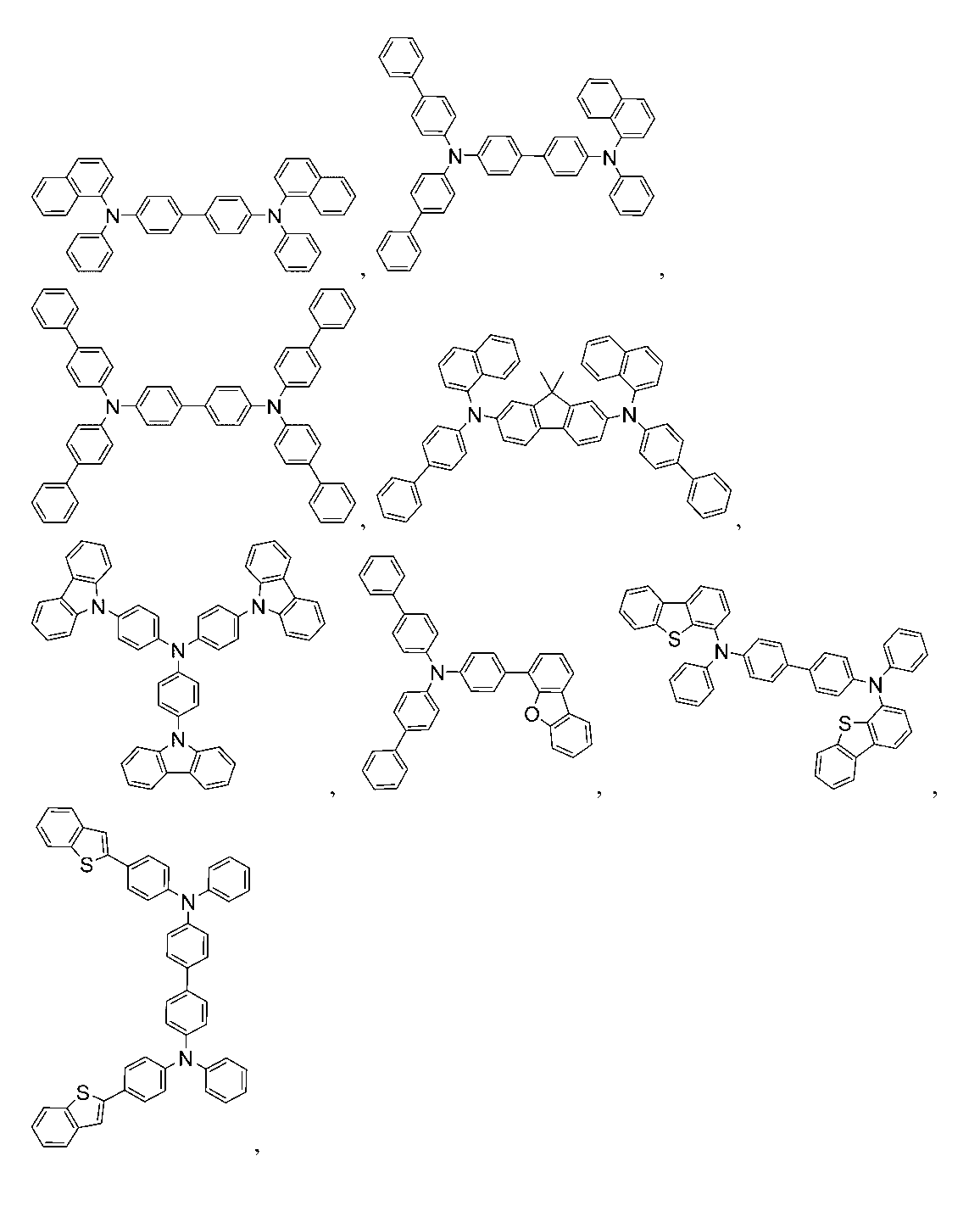

CN102702075、DE102012005215、EP01624500、EP01698613、EP01806334、EP01930964、EP01972613、EP01997799、EP02011790、EP02055700、EP02055701、EP1725079、EP2085382、EP2660300、EP650955、JP07-073529、JP2005112765、JP2007091719、JP2008021687、JP2014-009196、KR20110088898、KR20130077473、TW201139402、 US06517957、US20020158242、US20030162053、US20050123751、US20060182993、US20060240279、US20070145888、US20070181874、US20070278938、US20080014464、US20080091025、US20080106190、US20080124572、US20080145707、US20080220265、US20080233434、US20080303417、US2008107919、US20090115320、US20090167161、US2009066235、US2011007385、US20110163302、US2011240968、US2011278551、 US2012205642、US2013241401、US20140117329、US2014183517、US5061569、US5639914、WO05075451、WO07125714、WO08023550、WO08023759、WO2009145016、WO2010061824、WO2011075644、WO2012177006、WO2013018530、WO2013039073、WO2013087142、WO2013118812、WO2013120577、WO2013157367、WO2013175747、WO2014002873、WO2014015935、WO2014015937、WO2014030872、 WO2014030921, WO2014034791, WO2014104514, WO2014157018
電子ブロキング層(EBL)は、発光層から出る電子及び/又は励起子の数を減らすために使用されることができる。デバイス中のそのようなブロッキング層の存在は、ブロッキング層を欠く同様のデバイスと比較して、大幅に高い効率及び/又はより長い寿命をもたらし得る。また、ブロッキング層を使用して、OLEDの所望の領域に発光を制限することもできる。幾つかの実施形態においては、EBL材料は、EBLインターフェースに最も近接した発光体よりも高いLUMO(真空準位により近い)及び/又は高い三重項エネルギーを有する。幾つかの実施形態においては、EBL材料は、EBLインターフェースに最も近接したホストの1つ以上よりも高いLUMO(真空準位により近い)及び/又は高い三重項エネルギーを有する。1つの態様においては、EBL中に用いられる前記化合物は、下記に記載されるホストの1つとして、同じ分子又は同じ官能基を含む。
更なるホスト:
An electron blocking layer (EBL) can be used to reduce the number of electrons and/or excitons exiting the emissive layer. The presence of such blocking layers in devices can result in significantly higher efficiencies and/or longer lifetimes compared to similar devices lacking blocking layers. Blocking layers can also be used to restrict emission to desired areas of the OLED. In some embodiments, the EBL material has a higher LUMO (closer to vacuum level) and/or higher triplet energy than the emitter closest to the EBL interface. In some embodiments, the EBL material has a higher LUMO (closer to vacuum level) and/or higher triplet energy than one or more of the hosts closest to the EBL interface. In one aspect, the compound used in EBL contains the same molecule or the same functional group as one of the hosts described below.
Further hosts:
本発明の有機ELデバイスの発光層は、発光ドーパント材料として少なくとも金属錯体を含むことが好ましく、前記金属錯体をドーパント材料として用いる1つ以上の追加のホスト材料を含んでいてもよい。前記ホスト材料の例は、特に限定されず、ホストの三重項エネルギーがドーパントのものより大きい限り、任意の金属錯体又は有機化合物を使用してよい。三重項の基準が満たされれば、いずれのホスト材料もいずれのドーパントと共に用いられてもよい。 The light-emitting layer of the organic EL device of the present invention preferably contains at least a metal complex as a light-emitting dopant material and may contain one or more additional host materials using said metal complexes as dopant materials. Examples of the host material are not particularly limited, and any metal complex or organic compound may be used as long as the triplet energy of the host is greater than that of the dopant. Any host material may be used with any dopant, provided that the triplet criteria are met.
ホスト材料として使用される金属錯体の例は、下記の一般式を有することが好ましい。

一態様において、金属錯体は、下記の錯体である。

別の態様において、Metは、Ir及びPtから選択される。更なる態様において、(Y103-Y104)はカルベン配位子である。 In another aspect, Met is selected from Ir and Pt. In a further aspect, (Y 103 -Y 104 ) is a carbene ligand.
追加のホスト材料として使用される他の有機化合物の例は、ベンゼン、ビフェニル、トリフェニル、トリフェニレン、ナフタレン、アントラセン、フェナレン、フェナントレン、フルオレン、ピレン、クリセン、ペリレン、アズレン等の芳香族炭化水素環式化合物からなる群;ジベンゾチオフェン、ジベンゾフラン、ジベンゾセレノフェン、フラン、チオフェン、ベンゾフラン、ベンゾチオフェン、ベンゾセレノフェン、カルバゾール、インドロカルバゾール、ピリジルインドール、ピロロジピリジン、ピラゾール、イミダゾール、トリアゾール、オキサゾール、チアゾール、オキサジアゾール、オキサトリアゾール、ジオキサゾール、チアジアゾール、ピリジン、ピリダジン、ピリミジン、ピラジン、トリアジン、オキサジン、オキサチアジン、オキサジアジン、インドール、ベンズイミダゾール、インダゾール、インドキサジン、ベンゾオキサゾール、ベンズイソオキサゾール、ベンゾチアゾール、キノリン、イソキノリン、シンノリン、キナゾリン、キノキサリン、ナフチリジン、フタラジン、プテリジン、キサンテン、アクリジン、フェナジン、フェノチアジン、フェノキサジン、ベンゾフロピリジン、フロジピリジン、ベンゾチエノピリジン、チエノジピリジン、ベンゾセレノフェノピリジン及びセレノフェノジピリジン等の芳香族複素環式化合物からなる群;並びに芳香族炭化水素環式基及び芳香族複素環式基から選択される同じ種類又は異なる種類の基であり、且つ、直接的に、又は酸素原子、窒素原子、硫黄原子、ケイ素原子、リン原子、ホウ素原子、鎖構造単位及び脂肪族環式基の少なくとも1つを介して互いに結合している2から10個の環式構造単位からなる群から選択される。ここで、各基は、水素、重水素、ハライド、アルキル、シクロアルキル、ヘテロアルキル、アリールアルキル、アルコキシ、アリールオキシ、アミノ、シリル、アルケニル、シクロアルケニル、ヘテロアルケニル、アルキニル、アリール、ヘテロアリール、アシル、カルボニル、カルボン酸、エステル、ニトリル、イソニトリル、スルファニル、スルフィニル、スルフォニル、ホスフィノ、及びこれらの組み合わせからなる群から選択される置換基によって更に置換される。 Examples of other organic compounds used as additional host materials are aromatic hydrocarbon rings such as benzene, biphenyl, triphenyl, triphenylene, naphthalene, anthracene, phenalene, phenanthrene, fluorene, pyrene, chrysene, perylene, azulene. The group consisting of the compounds; dibenzothiophene, dibenzofuran, dibenzoselenophene, furan, thiophene, benzofuran, benzothiophene, benzoselenophene, carbazole, indolocarbazole, pyridylindole, pyrrolodipyridine, pyrazole, imidazole, triazole, oxazole, thiazole, Oxadiazole, oxatriazole, dioxazole, thiadiazole, pyridine, pyridazine, pyrimidine, pyrazine, triazine, oxazine, oxathiazine, oxadiazine, indole, benzimidazole, indazole, indoxazine, benzoxazole, benzisoxazole, benzothiazole, quinoline, isoquinoline , cinnoline, quinazoline, quinoxaline, naphthyridine, phthalazine, pteridine, xanthene, acridine, phenazine, phenothiazine, phenoxazine, benzofuropyridine, flodipyridine, benzothienopyridine, thienodipyridine, benzoselenophenopyridine and selenophenodipyridine. and groups of the same or different types selected from aromatic hydrocarbon cyclic groups and aromatic heterocyclic groups, and either directly or an oxygen atom, a nitrogen atom, a sulfur atom , a silicon atom, a phosphorus atom, a boron atom, a chain structure unit, and 2 to 10 cyclic structural units bonded to each other through at least one of an aliphatic cyclic group. wherein each group is hydrogen, deuterium, halide, alkyl, cycloalkyl, heteroalkyl, arylalkyl, alkoxy, aryloxy, amino, silyl, alkenyl, cycloalkenyl, heteroalkenyl, alkynyl, aryl, heteroaryl, acyl , carbonyl, carboxylic acid, ester, nitrile, isonitrile, sulfanyl, sulfinyl, sulfonyl, phosphino, and combinations thereof.
一つの態様においては、ホスト化合物は、分子中に、下記基の少なくとも1つを含む。


本明細書において開示されるホスト材料と組み合わせて、OLED中に用いられることができる追加のホスト材料の非制限的な例は、これらの材料を開示する文献と共に下記に例示される。
EP2034538、EP2034538A、EP2757608、JP2007254297、KR20100079458、KR20120088644、KR20120129733、KR20130115564、TW201329200、US20030175553、US20050238919、US20060280965、US20090017330、US20090030202、US20090167162、US20090302743、US20090309488、US20100012931、US20100084966、US20100187984、US2010187984、US2012075273、US2012126221、US2013009543、US2013105787、US2013175519、US2014001446、US20140183503、US20140225088、US2014034914、US7154114、WO2001039234、WO2004093207、WO2005014551、WO2005089025、WO2006072002、WO2006114966、WO2007063754、WO2008056746、WO2009003898、WO2009021126、WO2009063833、WO2009066778、WO2009066779、WO2009086028、WO2010056066、WO2010107244、WO2011081423、WO2011081431、WO2011086863、WO2012128298、WO2012133644、WO2012133649、WO2013024872、WO2013035275、WO2013081315、WO2013191404、WO2014142472、US20170263869、US20160163995、US9466803。


EP2034538、EP2034538A、EP2757608、JP2007254297、KR20100079458、KR20120088644、KR20120129733、KR20130115564、TW201329200、US20030175553、US20050238919、US20060280965、US20090017330、US20090030202、US20090167162、US20090302743、US20090309488、US20100012931、US20100084966、US20100187984、US2010187984、US2012075273、US2012126221、US2013009543、US2013105787、 US2013175519、US2014001446、US20140183503、US20140225088、US2014034914、US7154114、WO2001039234、WO2004093207、WO2005014551、WO2005089025、WO2006072002、WO2006114966、WO2007063754、WO2008056746、WO2009003898、WO2009021126、WO2009063833、WO2009066778、WO2009066779、WO2009086028、WO2010056066、WO2010107244、WO2011081423、WO2011081431、WO2011086863、 WO2012128298, WO2012133644, WO2012133649, WO2013024872, WO2013035275, WO2013081315, WO2013191404, WO2014142472, US20170263869, US20196860393.
発光体の例としては、特に限定されず、前記化合物が典型的に発光体材料として用いられるものであれば、いずれの化合物も用いられることができる。好適な発光体材料としては、リン光、蛍光、熱活性化遅延蛍光、即ちTADF(E型遅延蛍光とも称される;その全体を参照により本明細書に援用する米国出願第15/700,352号を参照)、三重項-三重項消滅、又はこれらの過程の組合せを介して、発光を生成することができる化合物が挙げられるが、これらに限定されない。 Examples of the light emitter are not particularly limited, and any compound can be used as long as the above compound is typically used as a light emitter material. Suitable emitter materials include phosphorescence, fluorescence, thermally activated delayed fluorescence, or TADF (also called E-type delayed fluorescence; US Application No. 15/700,352, which is incorporated herein by reference in its entirety) ), triplet-triplet annihilation, or a combination of these processes to produce luminescence.
本明細書において開示される材料と組み合わせて、OLED中に用いられることができる発光体材料の非制限的な例は、これらの材料を開示する文献と共に下記に例示される。
CN103694277、CN1696137、EB01238981、EP01239526、EP01961743、EP1239526、EP1244155、EP1642951、EP1647554、EP1841834、EP1841834B、EP2062907、EP2730583、JP2012074444、JP2013110263、JP4478555、KR1020090133652、KR20120032054、KR20130043460、TW201332980、US06699599、US06916554、US20010019782、US20020034656、US20030068526、US20030072964、US20030138657、US20050123788、US20050244673、US2005123791、US2005260449、US20060008670、US20060065890、US20060127696、US20060134459、US20060134462、US20060202194、US20060251923、US20070034863、US20070087321、US20070103060、US20070111026、US20070190359、US20070231600、US2007034863、US2007104979、US2007104980、US2007138437、US2007224450、US2007278936、US20080020237、US20080233410、US20080261076、US20080297033、US200805851、US2008161567、US2008210930、US20090039776、US20090108737、US20090115322、US20090179555、US2009085476、US2009104472、US20100090591、US20100148663、US20100244004、US20100295032、US2010102716、US2010105902、US2010244004、US2010270916、US20110057559、US20110108822、US20110204333、US2011215710、US2011227049、US2011285275、US2012292601、US20130146848、US2013033172、US2013165653、US2013181190、US2013334521、US20140246656、US2014103305、US6303238、US6413656、US6653654、US6670645、US6687266、US6835469、US6921915、US7279704、US7332232、US7378162、US7534505、US7675228、US7728137、US7740957、US7759489、US7951947、US8067099、US8592586、US8871361、WO06081973、WO06121811、WO07018067、WO07108362、WO07115970、WO07115981、WO08035571、WO2002015645、WO2003040257、WO2005019373、WO2006056418、WO2008054584、WO2008078800、WO2008096609、WO2008101842、WO2009000673、WO2009050281、WO2009100991、WO2010028151、WO2010054731、WO2010086089、WO2010118029、WO2011044988、WO2011051404、WO2011107491、WO2012020327、WO2012163471、WO2013094620、WO2013107487、WO2013174471、WO2014007565、WO2014008982、WO2014023377、WO2014024131、WO2014031977、WO2014038456、WO2014112450


CN103694277、CN1696137、EB01238981、EP01239526、EP01961743、EP1239526、EP1244155、EP1642951、EP1647554、EP1841834、EP1841834B、EP2062907、EP2730583、JP2012074444、JP2013110263、JP4478555、KR1020090133652、KR20120032054、KR20130043460、TW201332980、US06699599、US06916554、US20010019782、US20020034656、US20030068526、 US20030072964、US20030138657、US20050123788、US20050244673、US2005123791、US2005260449、US20060008670、US20060065890、US20060127696、US20060134459、US20060134462、US20060202194、US20060251923、US20070034863、US20070087321、US20070103060、US20070111026、US20070190359、US20070231600、US2007034863、US2007104979、US2007104980、US2007138437、US2007224450、US2007278936、 US20080020237、US20080233410、US20080261076、US20080297033、US200805851、US2008161567、US2008210930、US20090039776、US20090108737、US20090115322、US20090179555、US2009085476、US2009104472、US20100090591、US20100148663、US20100244004、US20100295032、US2010102716、US2010105902、US2010244004、US2010270916、US20110057559、US20110108822、US20110204333、US2011215710、 US2011227049, US2011285275, U S2012292601、US20130146848、US2013033172、US2013165653、US2013181190、US2013334521、US20140246656、US2014103305、US6303238、US6413656、US6653654、US6670645、US6687266、US6835469、US6921915、US7279704、US7332232、US7378162、US7534505、US7675228、US7728137、US7740957、US7759489、US7951947、US8067099、 US8592586、US8871361、WO06081973、WO06121811、WO07018067、WO07108362、WO07115970、WO07115981、WO08035571、WO2002015645、WO2003040257、WO2005019373、WO2006056418、WO2008054584、WO2008078800、WO2008096609、WO2008101842、WO2009000673、WO2009050281、WO2009100991、WO2010028151、WO2010054731、WO2010086089、WO2010118029、WO2011044988、 WO2011051404、WO2011107491、WO2012020327、WO2012163471、WO2013094620、WO2013107487、WO2013174471、WO2014007565、WO2014008982、WO2014023377、WO2014024131、WO2014031977、WO2014038456、WO2014112450
正孔ブロッキング層(HBL)を使用して、発光層から出る正孔及び/又は励起子の数を低減させることができる。デバイス中のそのようなブロッキング層の存在は、ブロッキング層を欠く同様のデバイスと比較して大幅に高い効率及び/又はより長い寿命をもたらし得る。また、ブロッキング層を使用して、OLEDの所望の領域に発光を制限することもできる。幾つかの実施形態においては、HBL材料は、HBLインターフェースに最も近接した発光体よりも低いHOMO(真空準位から更に離れて)及び/又は高い三重項エネルギーを有する。幾つかの実施形態においては、HBL材料は、HBLインターフェースに最も近接したホストの1つ以上よりも低いHOMO(真空準位から更に離れて)及び/又は高い三重項エネルギーを有する。 A hole blocking layer (HBL) can be used to reduce the number of holes and/or excitons exiting the emissive layer. The presence of such blocking layers in devices can result in significantly higher efficiencies and/or longer lifetimes compared to similar devices lacking blocking layers. Blocking layers can also be used to restrict emission to desired areas of the OLED. In some embodiments, the HBL material has a lower HOMO (further away from vacuum level) and/or a higher triplet energy than the emitter closest to the HBL interface. In some embodiments, the HBL material has a lower HOMO (further away from vacuum level) and/or a higher triplet energy than one or more of the hosts closest to the HBL interface.
一態様において、前記HBL中に使用される前記化合物は、上述したホストとして使用されるものと同じ分子を含有する。 In one aspect, the compound used in the HBL contains the same molecule used as the host described above.
別の態様において、前記HBL中に使用される前記化合物は、分子中に下記の群の少なくとも1つを含有する。

ETL:
In another embodiment, said compound used in said HBL contains at least one of the following groups in the molecule.
ETLs:
電子輸送層(ETL)は、電子を輸送することができる材料を含み得る。電子輸送層は、真性である(ドープされていない)か、又はドープされていてよい。ドーピングを使用して、伝導性を増強することができる。ETL材料の例は特に限定されず、電子を輸送するために典型的に使用されるものである限り、任意の金属錯体又は有機化合物を使用してよい。 An electron transport layer (ETL) may comprise a material capable of transporting electrons. The electron transport layer may be intrinsic (undoped) or doped. Doping can be used to enhance conductivity. Examples of ETL materials are not particularly limited, and any metal complex or organic compound typically used to transport electrons may be used.
一態様において、前記ETL中に使用される前記化合物は、分子中に下記の群の少なくとも1つを含有する。

別の態様において、前記ETL中に使用される金属錯体は、下記の一般式を含有するがこれらに限定されない。

本明細書において開示される材料と組み合わせて、OLED中に用いられることができるETL材料の非制限的な例は、これらの材料を開示する文献と共に下記に例示される。CN103508940、EP01602648、EP01734038、EP01956007、JP2004-022334、JP2005149918、JP2005-268199、KR0117693、KR20130108183、US20040036077、US20070104977、US2007018155、US20090101870、US20090115316、US20090140637、US20090179554、US2009218940、US2010108990、US2011156017、US2011210320、US2012193612、US2012214993、US2014014925、US2014014927、US20140284580、US6656612、US8415031、WO2003060956、WO2007111263、WO2009148269、WO2010067894、WO2010072300、WO2011074770、WO2011105373、WO2013079217、WO2013145667、WO2013180376、WO2014104499、WO2014104535.


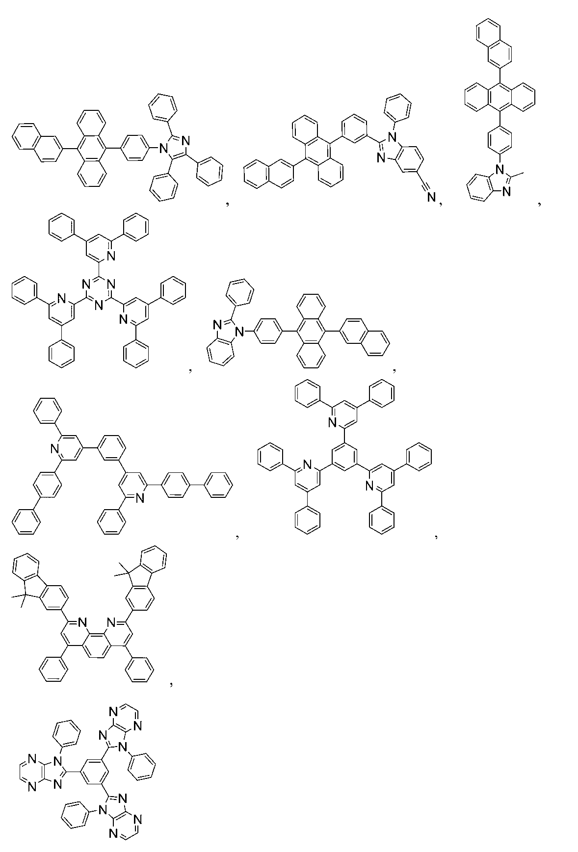
タンデム型、又は積層型のOLED中で、CGLは、性能において重要な役割を果たし、それぞれ、電子及び正孔の注入ためのn-ドープ層及びp-ドープ層からなる。電子及び正孔は、前記CGL及び電極から供給される。前記CGL中の消費された電子及び正孔は、それぞれカソード及びアノードから注入された電子及び正孔によって再び満たされ、その後バイポーラ電流が徐々に安定した状態に達する。典型的なCGL材料は、輸送層で用いられるn型及びp型伝導性ドーパントを含む。 In tandem or stacked OLEDs, CGLs play an important role in performance and consist of n- and p-doped layers for injection of electrons and holes, respectively. Electrons and holes are supplied from the CGL and electrodes. The consumed electrons and holes in the CGL are refilled by electrons and holes injected from the cathode and anode respectively, after which the bipolar current gradually reaches a steady state. A typical CGL material includes n-type and p-type conductive dopants used in the transport layer.
OLEDデバイスの各層中に使用される任意の上記で言及した化合物において、水素原子は、部分的に又は完全に重水素化されていてよい。故に、メチル、フェニル、ピリジル等であるがこれらに限定されない任意の具体的に挙げられている置換基は、それらの重水素化されていない、部分的に重水素化された、及び完全に重水素化されたバージョンを包含する。同様に、アルキル、アリール、シクロアルキル、ヘテロアリール等であるがこれらに限定されない置換基のクラスは、それらの重水素化されていない、部分的に重水素化された、及び完全に重水素化されたバージョンも包含する。 In any of the above-mentioned compounds used in each layer of an OLED device, the hydrogen atoms may be partially or fully deuterated. Thus, any specifically recited substituents such as, but not limited to, methyl, phenyl, pyridyl, etc., may be deuterated, partially deuterated, and fully deuterated. Includes hydrogenated versions. Similarly, classes of substituents such as, but not limited to, alkyl, aryl, cycloalkyl, heteroaryl, etc., include those deuterated, partially deuterated, and fully deuterated It also includes versions that have been modified.
本明細書において記述されている種々の実施形態は、単なる一例としてのものであり、本発明の範囲を限定することを意図するものではないことが理解される。例えば、本明細書において記述されている材料及び構造の多くは、本発明の趣旨から逸脱することなく他の材料及び構造に置き換えることができる。したがって、特許請求されている通りの本発明は、当業者には明らかとなるように、本明細書において記述されている特定の例及び好ましい実施形態からの変形形態を含み得る。なぜ本発明が作用するのかについての種々の理論は限定を意図するものではないことが理解される。 It is understood that the various embodiments described herein are by way of example only and are not intended to limit the scope of the invention. For example, many of the materials and structures described herein can be replaced with other materials and structures without departing from the spirit of the invention. Accordingly, the invention as claimed may include variations from the specific examples and preferred embodiments described herein, as will be apparent to those skilled in the art. It is understood that various theories as to why the invention works are not intended to be limiting.
100 有機発光デバイス
110 基板
115 アノード
120 正孔注入層
125 正孔輸送層
130 電子ブロッキング層
135 発光層
140 正孔ブロッキング層
145 電子輸送層
150 電子注入層
155 保護層
160 カソード
162 第一の導電層
164 第二の導電層
170 バリア層
200 反転させたOLED、デバイス
210 基板
215 カソード
220 発光層
225 正孔輸送層
230 アノード
REFERENCE SIGNS
Claims (8)
カソードと、
前記アノードと前記カソードとの間に配された有機発光層とを含む有機発光デバイス(OLED)であって、前記有機発光層が、
最高被占分子軌道(HOMO)エネルギー、最低空分子軌道(LUMO)エネルギー、及びT1三重項エネルギーを有する第1のホストと、
最高被占分子軌道(HOMO)エネルギー、最低空分子軌道(LUMO)エネルギー、及びT1三重項エネルギーを有する発光体とを含み、
前記発光体が、リン光金属錯体及び遅延蛍光発光体からなる群から選択され、
前記第1のホストの前記T1三重項エネルギーであるEH1Tが、前記発光体の前記T1三重項エネルギーであるEETよりも高く、
EETは、少なくとも2.50eVであり、
前記第1のホストの前記LUMOエネルギーが、前記発光体の前記HOMOエネルギーよりも高く、
前記発光体の前記HOMOエネルギーと前記第1のホストの前記LUMOエネルギーとの間の差の絶対値が、ΔE1であり、
a≦ΔE1-EET≦bであり、
a≧0.05eV且つb≦0.60eVであり、
前記第1のホストが、ピリジン、ピリミジン、ピラジン、トリアジン、イミダゾール、アザ-トリフェニレン、アザ-カルバゾール、アザ-ジベンゾフラン、及びアザ-ジベンゾセレノフェンからなる群から選択される少なくとも1つの化学基を含み、
前記発光体が、式Pt(L1)2又はPt(L1)(L2)で表され、L1は、他のL1又はL2と結合し、四座配位子を形成してもよく、
L1、及びL2は、それぞれ独立して、下記からなる群から選択されることを特徴とするOLED。


Xは、BR’、NR’、PR’、O、S、Se、C=O、S=O、SO2、CR’R’’、SiR’R’’、及びGeR’R’’からなる群から選択され、
R’及びR’’は、縮合又は結合して環を形成してもよく、
Ra、Rb、Rc、及びRdは、それぞれ、モノ置換から可能な最大数の置換を表す、又は無置換を表してもよく、
R’、R’’、Ra、Rb、Rc、及びRdは、それぞれ独立して、水素、重水素、ハロゲン、アルキル、シクロアルキル、ヘテロアルキル、ヘテロシクロアルキル、アリールアルキル、アルコキシ、アリールオキシ、アミノ、環状アミノ、シリル、アルケニル、シクロアルケニル、ヘテロアルケニル、アルキニル、アリール、ヘテロアリール、アシル、カルボニル、カルボン酸、エーテル、エステル、ニトリル、イソニトリル、スルファニル、スルフィニル、スルフォニル、ホスフィノ、及びこれらの組合せからなる群から選択され;
任意の2つのRa、Rb、Rc、及びRdは、縮合又は結合して環を形成する、又は多座配位子を形成してもよい。) an anode;
a cathode;
An organic light emitting device (OLED) comprising an organic light emitting layer disposed between the anode and the cathode, the organic light emitting layer comprising:
a first host having the highest occupied molecular orbital (HOMO) energy, the lowest unoccupied molecular orbital (LUMO) energy, and a T1 triplet energy;
an emitter having the highest occupied molecular orbital (HOMO) energy, the lowest unoccupied molecular orbital (LUMO) energy, and the T1 triplet energy;
the emitter is selected from the group consisting of phosphorescent metal complexes and delayed fluorescence emitters;
wherein the T1 triplet energy EH1T of the first host is higher than the T1 triplet energy EET of the emitter;
E ET is at least 2.50 eV;
the LUMO energy of the first host is higher than the HOMO energy of the light emitter;
the absolute value of the difference between the HOMO energy of the emitter and the LUMO energy of the first host is ΔE1;
a≦ΔE1−E ET ≦b,
a≧0.05 eV and b≦0.60 eV,
said first host comprises at least one chemical group selected from the group consisting of pyridine, pyrimidine, pyrazine, triazine, imidazole, aza-triphenylene, aza-carbazole, aza-dibenzofuran, and aza-dibenzoselenophene;
The light emitter may be represented by the formula Pt(L 1 ) 2 or Pt(L 1 )(L 2 ), where L 1 may combine with another L 1 or L 2 to form a tetradentate ligand. Often,
An OLED, wherein L 1 and L 2 are each independently selected from the group consisting of:
X is the group consisting of BR', NR', PR', O, S, Se, C=O, S=O, SO2, CR'R '', SiR'R'', and GeR'R'' is selected from
R' and R'' may be fused or combined to form a ring,
R a , R b , R c , and R d may each represent the maximum possible number of substitutions from mono-substitution, or may represent no substitution;
R′, R″, R a , R b , R c , and R d are each independently hydrogen, deuterium, halogen, alkyl, cycloalkyl, heteroalkyl, heterocycloalkyl, arylalkyl, alkoxy, aryloxy, amino, cyclic amino, silyl, alkenyl, cycloalkenyl, heteroalkenyl, alkynyl, aryl, heteroaryl, acyl, carbonyl, carboxylic acid, ether, ester, nitrile, isonitrile, sulfanyl, sulfinyl, sulfonyl, phosphino, and these selected from the group consisting of combinations of
Any two of R a , R b , R c and R d may be fused or combined to form a ring or form a multidentate ligand. )
前記第2のホストのT1三重項エネルギーであるEH2Tが、EETよりも高い、又は
前記第2のホストのHOMOエネルギーが、前記第1のホストの前記HOMOエネルギーよりも低く、前記第2のホストのLUMOエネルギーが、前記第1のホストの前記LUMOエネルギーよりも高い、又は
前記第2のホストのHOMOエネルギーが、前記第1のホストの前記HOMOエネルギーよりも高く、前記第2のホストのLUMOエネルギーが、前記第1のホストの前記LUMOエネルギーよりも高い請求項1に記載のOLED。 the OLED further comprising a second host;
The T 1 triplet energy of the second host, E H2T , is higher than E ET , or the HOMO energy of the second host is lower than the HOMO energy of the first host, and the second host the LUMO energy of the host is higher than the LUMO energy of the first host, or the HOMO energy of the second host is higher than the HOMO energy of the first host and the HOMO energy of the second host is 2. OLED according to claim 1, wherein the LUMO energy is higher than the LUMO energy of the first host.

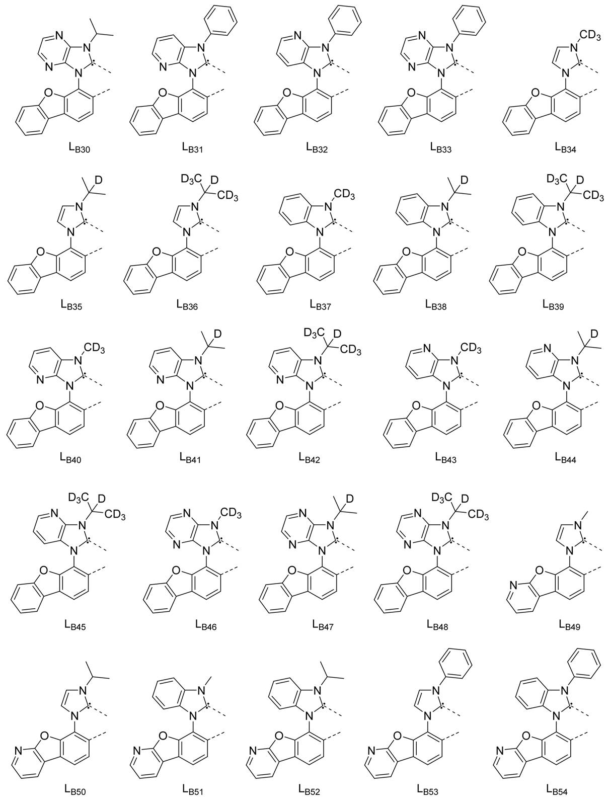


Priority Applications (1)
| Application Number | Priority Date | Filing Date | Title |
|---|---|---|---|
| JP2022209151A JP2023040097A (en) | 2017-07-26 | 2022-12-27 | Organic electroluminescent materials and devices |
Applications Claiming Priority (4)
| Application Number | Priority Date | Filing Date | Title |
|---|---|---|---|
| US201762537029P | 2017-07-26 | 2017-07-26 | |
| US62/537,029 | 2017-07-26 | ||
| US16/037,167 US11228010B2 (en) | 2017-07-26 | 2018-07-17 | Organic electroluminescent materials and devices |
| US16/037,167 | 2018-07-17 |
Related Child Applications (1)
| Application Number | Title | Priority Date | Filing Date |
|---|---|---|---|
| JP2022209151A Division JP2023040097A (en) | 2017-07-26 | 2022-12-27 | Organic electroluminescent materials and devices |
Publications (2)
| Publication Number | Publication Date |
|---|---|
| JP2019062184A JP2019062184A (en) | 2019-04-18 |
| JP7203526B2 true JP7203526B2 (en) | 2023-01-13 |
Family
ID=63173939
Family Applications (2)
| Application Number | Title | Priority Date | Filing Date |
|---|---|---|---|
| JP2018138172A Active JP7203526B2 (en) | 2017-07-26 | 2018-07-24 | Organic electroluminescent materials and devices |
| JP2022209151A Pending JP2023040097A (en) | 2017-07-26 | 2022-12-27 | Organic electroluminescent materials and devices |
Family Applications After (1)
| Application Number | Title | Priority Date | Filing Date |
|---|---|---|---|
| JP2022209151A Pending JP2023040097A (en) | 2017-07-26 | 2022-12-27 | Organic electroluminescent materials and devices |
Country Status (5)
| Country | Link |
|---|---|
| US (1) | US11228010B2 (en) |
| EP (2) | EP3435438B1 (en) |
| JP (2) | JP7203526B2 (en) |
| KR (2) | KR102535091B1 (en) |
| CN (2) | CN109309168B (en) |
Families Citing this family (33)
| Publication number | Priority date | Publication date | Assignee | Title |
|---|---|---|---|---|
| KR102395782B1 (en) | 2017-07-31 | 2022-05-09 | 삼성전자주식회사 | Organic light emitting device |
| US11700765B2 (en) * | 2018-01-10 | 2023-07-11 | Universal Display Corporation | Organic electroluminescent materials and devices |
| US11081659B2 (en) * | 2018-01-10 | 2021-08-03 | Universal Display Corporation | Organic electroluminescent materials and devices |
| KR102637792B1 (en) * | 2018-03-22 | 2024-02-19 | 삼성디스플레이 주식회사 | Organic light emitting device and electronic device including the same |
| US11672165B2 (en) * | 2018-11-28 | 2023-06-06 | Universal Display Corporation | Organic electroluminescent materials and devices |
| US11672176B2 (en) * | 2018-11-28 | 2023-06-06 | Universal Display Corporation | Host materials for electroluminescent devices |
| US11515489B2 (en) | 2018-11-28 | 2022-11-29 | Universal Display Corporation | Host materials for electroluminescent devices |
| US11690285B2 (en) * | 2018-11-28 | 2023-06-27 | Universal Display Corporation | Electroluminescent devices |
| US11716899B2 (en) * | 2018-11-28 | 2023-08-01 | Universal Display Corporation | Organic electroluminescent materials and devices |
| EP3670520B1 (en) * | 2018-12-19 | 2022-01-12 | Samsung Electronics Co., Ltd. | Organometallic compound, organic light-emitting device including the organometallic compound, and diagnostic composition including the organometallic compound |
| CN109748938B (en) * | 2019-02-01 | 2021-08-03 | 南京工业大学 | Bivalent platinum complex, application thereof and organic photoelectric device |
| US11512093B2 (en) | 2019-03-04 | 2022-11-29 | Universal Display Corporation | Compound used for organic light emitting device (OLED), consumer product and formulation |
| KR102608423B1 (en) * | 2019-03-28 | 2023-12-01 | 삼성디스플레이 주식회사 | Organic light emitting device and electronic apparatus |
| US11639363B2 (en) | 2019-04-22 | 2023-05-02 | Universal Display Corporation | Organic electroluminescent materials and devices |
| KR20200138568A (en) | 2019-05-31 | 2020-12-10 | 삼성디스플레이 주식회사 | Organic light emitting device and electronic apparatus |
| KR20210002984A (en) | 2019-07-01 | 2021-01-11 | 삼성전자주식회사 | Composition and organic light emitting device including the same |
| KR20210014813A (en) | 2019-07-30 | 2021-02-10 | 삼성디스플레이 주식회사 | Display device |
| US11925105B2 (en) * | 2019-08-26 | 2024-03-05 | Universal Display Corporation | Organic electroluminescent materials and devices |
| KR102505882B1 (en) | 2019-10-04 | 2023-03-06 | 삼성디스플레이 주식회사 | Organic light-emitting device and apparatus including the same |
| KR102505883B1 (en) | 2019-10-04 | 2023-03-06 | 삼성디스플레이 주식회사 | Organic light-emitting device and apparatus including the same |
| KR102544979B1 (en) | 2019-10-04 | 2023-06-20 | 삼성디스플레이 주식회사 | Organic light-emitting device and apparatus including the same |
| KR102505881B1 (en) | 2019-10-04 | 2023-03-06 | 삼성디스플레이 주식회사 | Organic light-emitting device and apparatus including the same |
| JP2021082801A (en) * | 2019-11-14 | 2021-05-27 | ユニバーサル ディスプレイ コーポレイション | Organic electroluminescence material and device |
| US20210171548A1 (en) * | 2019-11-27 | 2021-06-10 | Samsung Electronics Co., Ltd. | Organometallic compound, organic light-emitting device including organometallic compound and electronic apparatus including the organic light-emitting device |
| KR20210086219A (en) * | 2019-12-31 | 2021-07-08 | 엘지디스플레이 주식회사 | Organic electronic element, display panel comprising the same and display device comprising the same |
| KR20210136224A (en) | 2020-05-06 | 2021-11-17 | 삼성디스플레이 주식회사 | Llight emitting device and electronic apparatus comprising same |
| KR20210143379A (en) * | 2020-05-19 | 2021-11-29 | 삼성디스플레이 주식회사 | Organic light-emitting device and electronic apparatus including the same |
| KR20220010691A (en) * | 2020-07-17 | 2022-01-26 | 삼성디스플레이 주식회사 | Light emitting device and electronic apparatus comprising the device |
| CN111864095B (en) * | 2020-07-23 | 2023-04-28 | 京东方科技集团股份有限公司 | Organic light-emitting diode structure and display device |
| KR102493132B1 (en) * | 2020-09-11 | 2023-01-31 | 삼성디스플레이 주식회사 | Light-emitting device and electronic apparatus including the same |
| CN113013346B (en) * | 2021-02-25 | 2023-06-27 | 上海弗屈尔光电科技有限公司 | Ternary composition, organic electroluminescent element containing ternary composition and application of ternary composition |
| KR20220136951A (en) * | 2021-04-01 | 2022-10-11 | 삼성에스디아이 주식회사 | Composition for organic optoelectronic device, organic optoelectronic device and display device |
| JP7461095B1 (en) | 2022-09-15 | 2024-04-03 | 株式会社Kyulux | Organic light-emitting device, design method thereof and program |
Citations (7)
| Publication number | Priority date | Publication date | Assignee | Title |
|---|---|---|---|---|
| WO2007108362A1 (en) | 2006-03-17 | 2007-09-27 | Konica Minolta Holdings, Inc. | Organic electroluminescent device, display and illuminating device |
| JP2014168088A (en) | 2006-06-13 | 2014-09-11 | Konica Minolta Inc | Organic electroluminescent element |
| US20150295197A1 (en) | 2014-04-15 | 2015-10-15 | Universal Display Corporation | Efficient Organic Electroluminescent Devices |
| US20150380666A1 (en) | 2014-06-26 | 2015-12-31 | Universal Display Corporation | Organic electroluminescent materials and devices |
| CN105895820A (en) | 2016-06-21 | 2016-08-24 | 武汉华星光电技术有限公司 | Organic light emitting device and display device thereof |
| JP2017019761A (en) | 2015-07-15 | 2017-01-26 | 国立大学法人山形大学 | Novel terpyridine derivative, and electron transport material and organic el element prepared therewith |
| JP2017108108A (en) | 2015-09-30 | 2017-06-15 | 株式会社半導体エネルギー研究所 | Light-emitting element, display device, electronic apparatus, and lighting device |
Family Cites Families (356)
| Publication number | Priority date | Publication date | Assignee | Title |
|---|---|---|---|---|
| US4769292A (en) | 1987-03-02 | 1988-09-06 | Eastman Kodak Company | Electroluminescent device with modified thin film luminescent zone |
| GB8909011D0 (en) | 1989-04-20 | 1989-06-07 | Friend Richard H | Electroluminescent devices |
| US5061569A (en) | 1990-07-26 | 1991-10-29 | Eastman Kodak Company | Electroluminescent device with organic electroluminescent medium |
| JPH0773529A (en) | 1993-08-31 | 1995-03-17 | Hitachi Ltd | Magneto-optical recording system and magneto-optical recording medium |
| DE69412567T2 (en) | 1993-11-01 | 1999-02-04 | Hodogaya Chemical Co Ltd | Amine compound and electroluminescent device containing it |
| US5703436A (en) | 1994-12-13 | 1997-12-30 | The Trustees Of Princeton University | Transparent contacts for organic devices |
| US5707745A (en) | 1994-12-13 | 1998-01-13 | The Trustees Of Princeton University | Multicolor organic light emitting devices |
| KR0117693Y1 (en) | 1995-03-16 | 1998-04-23 | 천일선 | Opening and closing apparatus in a roaster |
| US6939625B2 (en) | 1996-06-25 | 2005-09-06 | Nôrthwestern University | Organic light-emitting diodes and methods for assembly and enhanced charge injection |
| US5844363A (en) | 1997-01-23 | 1998-12-01 | The Trustees Of Princeton Univ. | Vacuum deposited, non-polymeric flexible organic light emitting devices |
| US6091195A (en) | 1997-02-03 | 2000-07-18 | The Trustees Of Princeton University | Displays having mesa pixel configuration |
| US5834893A (en) | 1996-12-23 | 1998-11-10 | The Trustees Of Princeton University | High efficiency organic light emitting devices with light directing structures |
| US6013982A (en) | 1996-12-23 | 2000-01-11 | The Trustees Of Princeton University | Multicolor display devices |
| US6517957B1 (en) | 1997-05-19 | 2003-02-11 | Canon Kabushiki Kaisha | Organic compound and electroluminescent device using the same |
| US6413656B1 (en) | 1998-09-14 | 2002-07-02 | The University Of Southern California | Reduced symmetry porphyrin molecules for producing enhanced luminosity from phosphorescent organic light emitting devices |
| US6303238B1 (en) | 1997-12-01 | 2001-10-16 | The Trustees Of Princeton University | OLEDs doped with phosphorescent compounds |
| US6337102B1 (en) | 1997-11-17 | 2002-01-08 | The Trustees Of Princeton University | Low pressure vapor phase deposition of organic thin films |
| US6087196A (en) | 1998-01-30 | 2000-07-11 | The Trustees Of Princeton University | Fabrication of organic semiconductor devices using ink jet printing |
| US6528187B1 (en) | 1998-09-08 | 2003-03-04 | Fuji Photo Film Co., Ltd. | Material for luminescence element and luminescence element using the same |
| US6097147A (en) | 1998-09-14 | 2000-08-01 | The Trustees Of Princeton University | Structure for high efficiency electroluminescent device |
| US6830828B2 (en) | 1998-09-14 | 2004-12-14 | The Trustees Of Princeton University | Organometallic complexes as phosphorescent emitters in organic LEDs |
| US6461747B1 (en) | 1999-07-22 | 2002-10-08 | Fuji Photo Co., Ltd. | Heterocyclic compounds, materials for light emitting devices and light emitting devices using the same |
| US6294398B1 (en) | 1999-11-23 | 2001-09-25 | The Trustees Of Princeton University | Method for patterning devices |
| US6458475B1 (en) | 1999-11-24 | 2002-10-01 | The Trustee Of Princeton University | Organic light emitting diode having a blue phosphorescent molecule as an emitter |
| US6821645B2 (en) | 1999-12-27 | 2004-11-23 | Fuji Photo Film Co., Ltd. | Light-emitting material comprising orthometalated iridium complex, light-emitting device, high efficiency red light-emitting device, and novel iridium complex |
| KR100377321B1 (en) | 1999-12-31 | 2003-03-26 | 주식회사 엘지화학 | Electronic device comprising organic compound having p-type semiconducting characteristics |
| US6670645B2 (en) | 2000-06-30 | 2003-12-30 | E. I. Du Pont De Nemours And Company | Electroluminescent iridium compounds with fluorinated phenylpyridines, phenylpyrimidines, and phenylquinolines and devices made with such compounds |
| US20020121638A1 (en) | 2000-06-30 | 2002-09-05 | Vladimir Grushin | Electroluminescent iridium compounds with fluorinated phenylpyridines, phenylpyrimidines, and phenylquinolines and devices made with such compounds |
| JP2002050860A (en) | 2000-08-04 | 2002-02-15 | Toray Eng Co Ltd | Method and device for mounting |
| EP1325671B1 (en) | 2000-08-11 | 2012-10-24 | The Trustees Of Princeton University | Organometallic compounds and emission-shifting organic electrophosphorescence |
| KR100825182B1 (en) | 2000-11-30 | 2008-04-24 | 캐논 가부시끼가이샤 | Luminescent Element and Display |
| JP4154145B2 (en) | 2000-12-01 | 2008-09-24 | キヤノン株式会社 | Metal coordination compound, light emitting device and display device |
| US6579630B2 (en) | 2000-12-07 | 2003-06-17 | Canon Kabushiki Kaisha | Deuterated semiconducting organic compounds used for opto-electronic devices |
| JP3812730B2 (en) | 2001-02-01 | 2006-08-23 | 富士写真フイルム株式会社 | Transition metal complex and light emitting device |
| JP4307000B2 (en) | 2001-03-08 | 2009-08-05 | キヤノン株式会社 | Metal coordination compound, electroluminescent element and display device |
| JP4438042B2 (en) | 2001-03-08 | 2010-03-24 | キヤノン株式会社 | Metal coordination compound, electroluminescent element and display device |
| JP4307001B2 (en) | 2001-03-14 | 2009-08-05 | キヤノン株式会社 | Metal coordination compound, electroluminescent element and display device |
| DE10116962A1 (en) | 2001-04-05 | 2002-10-10 | Covion Organic Semiconductors | Rhodium and iridium complexes |
| JP4310077B2 (en) | 2001-06-19 | 2009-08-05 | キヤノン株式会社 | Metal coordination compound and organic light emitting device |
| CN100440568C (en) | 2001-06-20 | 2008-12-03 | 昭和电工株式会社 | Light emitting material and organic light-emitting device |
| US7071615B2 (en) | 2001-08-20 | 2006-07-04 | Universal Display Corporation | Transparent electrodes |
| US7250226B2 (en) | 2001-08-31 | 2007-07-31 | Nippon Hoso Kyokai | Phosphorescent compound, a phosphorescent composition and an organic light-emitting device |
| US7431968B1 (en) | 2001-09-04 | 2008-10-07 | The Trustees Of Princeton University | Process and apparatus for organic vapor jet deposition |
| US6835469B2 (en) | 2001-10-17 | 2004-12-28 | The University Of Southern California | Phosphorescent compounds and devices comprising the same |
| US7166368B2 (en) | 2001-11-07 | 2007-01-23 | E. I. Du Pont De Nemours And Company | Electroluminescent platinum compounds and devices made with such compounds |
| US6863997B2 (en) | 2001-12-28 | 2005-03-08 | The Trustees Of Princeton University | White light emitting OLEDs from combined monomer and aggregate emission |
| KR100691543B1 (en) | 2002-01-18 | 2007-03-09 | 주식회사 엘지화학 | New material for transporting electron and organic electroluminescent display using the same |
| US6653654B1 (en) | 2002-05-01 | 2003-11-25 | The University Of Hong Kong | Electroluminescent materials |
| JP4106974B2 (en) | 2002-06-17 | 2008-06-25 | コニカミノルタホールディングス株式会社 | Organic electroluminescence element and display device |
| US20030230980A1 (en) | 2002-06-18 | 2003-12-18 | Forrest Stephen R | Very low voltage, high efficiency phosphorescent oled in a p-i-n structure |
| US6916554B2 (en) | 2002-11-06 | 2005-07-12 | The University Of Southern California | Organic light emitting materials and devices |
| US7189989B2 (en) | 2002-08-22 | 2007-03-13 | Fuji Photo Film Co., Ltd. | Light emitting element |
| DE10238903A1 (en) | 2002-08-24 | 2004-03-04 | Covion Organic Semiconductors Gmbh | New heteroaromatic rhodium and iridium complexes, useful in electroluminescent and/or phosphorescent devices as the emission layer and for use in solar cells, photovoltaic devices and organic photodetectors |
| KR100686268B1 (en) | 2002-08-27 | 2007-02-28 | 후지필름 가부시키가이샤 | Organometallic Complexes, Organic EL Devices, and Organic EL Displays |
| JP4261855B2 (en) | 2002-09-19 | 2009-04-30 | キヤノン株式会社 | Phenanthroline compound and organic light emitting device using the same |
| US6687266B1 (en) | 2002-11-08 | 2004-02-03 | Universal Display Corporation | Organic light emitting materials and devices |
| JP4365199B2 (en) | 2002-12-27 | 2009-11-18 | 富士フイルム株式会社 | Organic electroluminescence device |
| JP4365196B2 (en) | 2002-12-27 | 2009-11-18 | 富士フイルム株式会社 | Organic electroluminescence device |
| DE10310887A1 (en) | 2003-03-11 | 2004-09-30 | Covion Organic Semiconductors Gmbh | Matallkomplexe |
| JP5095206B2 (en) | 2003-03-24 | 2012-12-12 | ユニバーシティ オブ サザン カリフォルニア | Phenyl and fluorenyl substituted phenyl-pyrazole complexes of iridium (Ir) |
| US7090928B2 (en) | 2003-04-01 | 2006-08-15 | The University Of Southern California | Binuclear compounds |
| EP1618170A2 (en) | 2003-04-15 | 2006-01-25 | Covion Organic Semiconductors GmbH | Mixtures of matrix materials and organic semiconductors capable of emission, use of the same and electronic components containing said mixtures |
| US7029765B2 (en) | 2003-04-22 | 2006-04-18 | Universal Display Corporation | Organic light emitting devices having reduced pixel shrinkage |
| US20060186791A1 (en) | 2003-05-29 | 2006-08-24 | Osamu Yoshitake | Organic electroluminescent element |
| JP2005011610A (en) | 2003-06-18 | 2005-01-13 | Nippon Steel Chem Co Ltd | Organic electroluminescent element |
| EP1647554B1 (en) | 2003-07-22 | 2011-08-31 | Idemitsu Kosan Co., Ltd. | Iridiumorganic complex and electroluminescent device using same |
| US20050025993A1 (en) | 2003-07-25 | 2005-02-03 | Thompson Mark E. | Materials and structures for enhancing the performance of organic light emitting devices |
| JP4561221B2 (en) | 2003-07-31 | 2010-10-13 | 三菱化学株式会社 | Compound, charge transport material and organic electroluminescence device |
| TWI390006B (en) | 2003-08-07 | 2013-03-21 | Nippon Steel Chemical Co | Organic EL materials with aluminum clamps |
| DE10338550A1 (en) | 2003-08-19 | 2005-03-31 | Basf Ag | Transition metal complexes with carbene ligands as emitters for organic light-emitting diodes (OLEDs) |
| US7504049B2 (en) | 2003-08-25 | 2009-03-17 | Semiconductor Energy Laboratory Co., Ltd. | Electrode device for organic device, electronic device having electrode device for organic device, and method of forming electrode device for organic device |
| HU0302888D0 (en) | 2003-09-09 | 2003-11-28 | Pribenszky Csaba Dr | In creasing of efficacity of stable storage by freezing of embryos in preimplantation stage with pretreatment by pressure |
| US20060269780A1 (en) | 2003-09-25 | 2006-11-30 | Takayuki Fukumatsu | Organic electroluminescent device |
| DE10345572A1 (en) | 2003-09-29 | 2005-05-19 | Covion Organic Semiconductors Gmbh | metal complexes |
| JP5112601B2 (en) | 2003-10-07 | 2013-01-09 | 三井化学株式会社 | Heterocyclic compound and organic electroluminescent device containing the compound |
| EP1683804B1 (en) | 2003-11-04 | 2013-07-31 | Takasago International Corporation | Platinum complex and luminescent element |
| JP4215621B2 (en) | 2003-11-17 | 2009-01-28 | 富士電機アセッツマネジメント株式会社 | External circuit handle device for circuit breaker |
| JP4822687B2 (en) | 2003-11-21 | 2011-11-24 | 富士フイルム株式会社 | Organic electroluminescence device |
| DE10357044A1 (en) | 2003-12-04 | 2005-07-14 | Novaled Gmbh | Process for doping organic semiconductors with quinonediimine derivatives |
| US20050123791A1 (en) | 2003-12-05 | 2005-06-09 | Deaton Joseph C. | Organic electroluminescent devices |
| US7029766B2 (en) | 2003-12-05 | 2006-04-18 | Eastman Kodak Company | Organic element for electroluminescent devices |
| US7332232B2 (en) | 2004-02-03 | 2008-02-19 | Universal Display Corporation | OLEDs utilizing multidentate ligand systems |
| TW200535134A (en) | 2004-02-09 | 2005-11-01 | Nippon Steel Chemical Co | Aminodibenzodioxin derivative and organic electroluminescent device using same |
| KR100882172B1 (en) | 2004-03-11 | 2009-02-06 | 미쓰비시 가가꾸 가부시키가이샤 | Composition for charge-transporting film and ion compound, charge-transporting film and organic electroluminescent device using same, and method for manufacturing organic electroluminescent device and method for producing charge-transporting film |
| TW200531592A (en) | 2004-03-15 | 2005-09-16 | Nippon Steel Chemical Co | Organic electroluminescent device |
| JP4869565B2 (en) | 2004-04-23 | 2012-02-08 | 富士フイルム株式会社 | Organic electroluminescence device |
| US7491823B2 (en) | 2004-05-18 | 2009-02-17 | The University Of Southern California | Luminescent compounds with carbene ligands |
| US7279704B2 (en) | 2004-05-18 | 2007-10-09 | The University Of Southern California | Complexes with tridentate ligands |
| US7154114B2 (en) | 2004-05-18 | 2006-12-26 | Universal Display Corporation | Cyclometallated iridium carbene complexes for use as hosts |
| US7445855B2 (en) | 2004-05-18 | 2008-11-04 | The University Of Southern California | Cationic metal-carbene complexes |
| US7534505B2 (en) | 2004-05-18 | 2009-05-19 | The University Of Southern California | Organometallic compounds for use in electroluminescent devices |
| US7393599B2 (en) | 2004-05-18 | 2008-07-01 | The University Of Southern California | Luminescent compounds with carbene ligands |
| WO2005123873A1 (en) | 2004-06-17 | 2005-12-29 | Konica Minolta Holdings, Inc. | Organic electroluminescent device material, organic electroluminescent device, display and illuminating device |
| WO2006000544A2 (en) | 2004-06-28 | 2006-01-05 | Ciba Specialty Chemicals Holding Inc. | Electroluminescent metal complexes with triazoles and benzotriazoles |
| US20060008670A1 (en) | 2004-07-06 | 2006-01-12 | Chun Lin | Organic light emitting materials and devices |
| US7504657B2 (en) | 2004-07-23 | 2009-03-17 | Konica Minolta Holdings, Inc. | Organic electroluminescent element, display and illuminator |
| US20060182993A1 (en) | 2004-08-10 | 2006-08-17 | Mitsubishi Chemical Corporation | Compositions for organic electroluminescent device and organic electroluminescent device |
| KR100880220B1 (en) | 2004-10-04 | 2009-01-28 | 엘지디스플레이 주식회사 | Iridium compound-based luminescence compounds comprising phenylpyridine groups with organic silicon and OLED using the same as luminous material |
| DE102004057072A1 (en) | 2004-11-25 | 2006-06-01 | Basf Ag | Use of Transition Metal Carbene Complexes in Organic Light Emitting Diodes (OLEDs) |
| US8021765B2 (en) | 2004-11-29 | 2011-09-20 | Samsung Mobile Display Co., Ltd. | Phenylcarbazole-based compound and organic electroluminescent device employing the same |
| JP4478555B2 (en) | 2004-11-30 | 2010-06-09 | キヤノン株式会社 | Metal complex, light emitting element and image display device |
| US20060134459A1 (en) | 2004-12-17 | 2006-06-22 | Shouquan Huo | OLEDs with mixed-ligand cyclometallated complexes |
| TWI242596B (en) | 2004-12-22 | 2005-11-01 | Ind Tech Res Inst | Organometallic compound and organic electroluminescent device including the same |
| JP5100395B2 (en) | 2004-12-23 | 2012-12-19 | チバ ホールディング インコーポレーテッド | Electroluminescent metal complexes with nucleophilic carbene ligands |
| EP1859656B1 (en) | 2004-12-30 | 2013-07-17 | E.I. Du Pont De Nemours And Company | Organometallic complexes |
| US20070181874A1 (en) | 2004-12-30 | 2007-08-09 | Shiva Prakash | Charge transport layers and organic electron devices comprising same |
| EP2371810A1 (en) | 2005-01-05 | 2011-10-05 | Idemitsu Kosan Co., Ltd. | Aromatic amine derivative and organic electroluminescent device using same |
| CN101115762A (en) | 2005-02-03 | 2008-01-30 | 默克专利有限公司 | Metal complexes |
| US8377571B2 (en) | 2005-02-04 | 2013-02-19 | Konica Minolta Holdings, Inc. | Material for organic electroluminescence element, organic electroluminescence element, display device and lighting device |
| WO2006081780A1 (en) | 2005-02-04 | 2006-08-10 | Novaled Ag | Dopants for organic semiconductors |
| KR100676965B1 (en) | 2005-03-05 | 2007-02-02 | 주식회사 두산 | Novel iridium complex and organic electroluminescence device using the same |
| KR100803125B1 (en) | 2005-03-08 | 2008-02-14 | 엘지전자 주식회사 | Red phosphorescent compounds and organic electroluminescence devices using the same |
| KR100797469B1 (en) | 2005-03-08 | 2008-01-24 | 엘지전자 주식회사 | Red phosphorescent compounds and organic electroluminescence devices using the same |
| JP5125502B2 (en) | 2005-03-16 | 2013-01-23 | コニカミノルタホールディングス株式会社 | Organic electroluminescence element material, organic electroluminescence element |
| DE102005014284A1 (en) | 2005-03-24 | 2006-09-28 | Basf Ag | Use of compounds containing aromatic or heteroaromatic rings containing groups via carbonyl groups as matrix materials in organic light-emitting diodes |
| WO2006103874A1 (en) | 2005-03-29 | 2006-10-05 | Konica Minolta Holdings, Inc. | Organic electroluminescent device material, organic electroluminescent device, display and illuminating device |
| WO2006114966A1 (en) | 2005-04-18 | 2006-11-02 | Konica Minolta Holdings, Inc. | Organic electroluminescent device, display and illuminating device |
| CN101180262B (en) | 2005-04-18 | 2012-06-13 | 出光兴产株式会社 | aromatic triamine compound and organic electroluminescent element using the same |
| US7807275B2 (en) | 2005-04-21 | 2010-10-05 | Universal Display Corporation | Non-blocked phosphorescent OLEDs |
| CN1321125C (en) | 2005-04-30 | 2007-06-13 | 中国科学院长春应用化学研究所 | Complexes of red light iridium by using nitrogen heterocycles in quinoline as ligand, and application |
| US7902374B2 (en) | 2005-05-06 | 2011-03-08 | Universal Display Corporation | Stability OLED materials and devices |
| US8586204B2 (en) | 2007-12-28 | 2013-11-19 | Universal Display Corporation | Phosphorescent emitters and host materials with improved stability |
| JP4533796B2 (en) | 2005-05-06 | 2010-09-01 | 富士フイルム株式会社 | Organic electroluminescence device |
| US9051344B2 (en) | 2005-05-06 | 2015-06-09 | Universal Display Corporation | Stability OLED materials and devices |
| KR101357475B1 (en) | 2005-05-31 | 2014-02-03 | 유니버셜 디스플레이 코포레이션 | Triphenylene hosts in phosphorescent light emitting diodes |
| KR101010846B1 (en) | 2005-06-07 | 2011-01-25 | 신닛테츠가가쿠 가부시키가이샤 | Organic metal complex and organic electroluminescent device using same |
| JP5324217B2 (en) | 2005-06-27 | 2013-10-23 | イー・アイ・デュポン・ドウ・ヌムール・アンド・カンパニー | Conductive polymer composition |
| US20090039771A1 (en) | 2005-07-01 | 2009-02-12 | Konica Minolta Holdings, Inc. | Organic electroluminescent element material, organic electroluminescent element, display device and lighting device |
| US20090140637A1 (en) | 2005-07-11 | 2009-06-04 | Idemitsu Kosan Co., Ltd. | Nitrogen-containing heterocyclic derivative having electron-attracting substituent and organic electroluminescence element using the same |
| KR20070009306A (en) * | 2005-07-15 | 2007-01-18 | 삼성에스디아이 주식회사 | White organic light-emitting devices |
| US8187727B2 (en) | 2005-07-22 | 2012-05-29 | Lg Chem, Ltd. | Imidazole derivatives, preparation method thereof and organic electronic device using the same |
| JP5317386B2 (en) | 2005-08-05 | 2013-10-16 | 出光興産株式会社 | Nitrogen-containing heterocyclic derivative and organic electroluminescence device using the same |
| WO2007018067A1 (en) | 2005-08-05 | 2007-02-15 | Idemitsu Kosan Co., Ltd. | Transition metal complex compound and organic electroluminescent device using same |
| JP4848152B2 (en) | 2005-08-08 | 2011-12-28 | 出光興産株式会社 | Aromatic amine derivative and organic electroluminescence device using the same |
| JP5040216B2 (en) | 2005-08-30 | 2012-10-03 | 三菱化学株式会社 | Organic compound, charge transport material, material for organic electroluminescence device, charge transport material composition, and organic electroluminescence device |
| WO2007028417A1 (en) | 2005-09-07 | 2007-03-15 | Technische Universität Braunschweig | Triplett emitter having condensed five-membered rings |
| JP4887731B2 (en) | 2005-10-26 | 2012-02-29 | コニカミノルタホールディングス株式会社 | Organic electroluminescence element, display device and lighting device |
| US9023489B2 (en) | 2005-11-07 | 2015-05-05 | Lg Display Co., Ltd. | Red phosphorescent compounds and organic electroluminescent devices using the same |
| US20070104977A1 (en) | 2005-11-07 | 2007-05-10 | Idemitsu Kosan Co., Ltd. | Organic electroluminescent device |
| KR100662378B1 (en) | 2005-11-07 | 2007-01-02 | 엘지전자 주식회사 | Red phosphorescene compounds and organic electroluminescence devices using the same |
| US7462406B2 (en) | 2005-11-15 | 2008-12-09 | Eastman Kodak Company | OLED devices with dinuclear copper compounds |
| US20070145888A1 (en) | 2005-11-16 | 2007-06-28 | Idemitsu Kosan Co., Ltd. | Aromatic amine derivatives and organic electroluminescence device using the same |
| US20080233410A1 (en) | 2005-11-17 | 2008-09-25 | Idemitsu Kosan Co., Ltd. | Transition metal complex compound |
| CN101371377A (en) | 2005-12-01 | 2009-02-18 | 新日铁化学株式会社 | Organic electroluminescent device |
| JP4593631B2 (en) | 2005-12-01 | 2010-12-08 | 新日鐵化学株式会社 | Compound for organic electroluminescence device and organic electroluminescence device |
| US7999103B2 (en) | 2005-12-15 | 2011-08-16 | Chuo University | Metal complex compound and organic electroluminescence device using the compound |
| WO2007080801A1 (en) | 2006-01-11 | 2007-07-19 | Idemitsu Kosan Co., Ltd. | Novel imide derivative, material for organic electroluminescent element, and organic electroluminescent element comprising the same |
| US7759489B2 (en) | 2006-01-27 | 2010-07-20 | Idemitsu Kosan Co., Ltd. | Transition metal complex compound and organic electroluminescence device using the compound |
| CN101415718B (en) | 2006-02-10 | 2013-05-29 | 通用显示公司 | Metal complexes of cyclometallated imidazo[1,2-f]phenanthridine and diimidazo[1,2-a:1',2'-c]quinazoline ligands and isoelectronic and benzannulated analogs thereof |
| US8142909B2 (en) | 2006-02-10 | 2012-03-27 | Universal Display Corporation | Blue phosphorescent imidazophenanthridine materials |
| JP4823730B2 (en) | 2006-03-20 | 2011-11-24 | 新日鐵化学株式会社 | Luminescent layer compound and organic electroluminescent device |
| DE502006000749D1 (en) | 2006-03-21 | 2008-06-19 | Novaled Ag | Heterocyclic radical or diradical, their dimers, oligomers, polymers, dispiro compounds and polycycles, their use, organic semiconducting material and electronic component |
| KR20070097139A (en) | 2006-03-23 | 2007-10-04 | 엘지전자 주식회사 | Red phosphorescene compounds and organic electroluminescence devices using the same |
| JPWO2007111263A1 (en) | 2006-03-27 | 2009-08-13 | 出光興産株式会社 | Nitrogen-containing heterocyclic derivative and organic electroluminescence device using the same |
| JP5273910B2 (en) | 2006-03-31 | 2013-08-28 | キヤノン株式会社 | Organic compound for light emitting element, light emitting element and image display device |
| WO2007115981A1 (en) | 2006-04-04 | 2007-10-18 | Basf Se | Transition metal complexes comprising one noncarbene ligand and one or two carbene ligands and their use in oleds |
| US10385263B2 (en) | 2006-04-05 | 2019-08-20 | Udc Ireland Limited | Heteroleptic transition metal-carbene complexes and their use in organic light-emitting diodes (OLEDS) |
| US20090128024A1 (en) | 2006-04-20 | 2009-05-21 | Kenichi Fukuoka | Organic light-emitting device |
| WO2007125714A1 (en) | 2006-04-26 | 2007-11-08 | Idemitsu Kosan Co., Ltd. | Aromatic amine derivative, and organic electroluminescence element using the same |
| WO2007132678A1 (en) | 2006-05-11 | 2007-11-22 | Idemitsu Kosan Co., Ltd. | Organic electroluminescent device |
| KR20090016684A (en) | 2006-06-02 | 2009-02-17 | 이데미쓰 고산 가부시키가이샤 | Material for organic electroluminescence element, and organic electroluminescence element using the material |
| US20070278936A1 (en) | 2006-06-02 | 2007-12-06 | Norman Herron | Red emitter complexes of IR(III) and devices made with such compounds |
| TW200815446A (en) | 2006-06-05 | 2008-04-01 | Idemitsu Kosan Co | Organic electroluminescent device and material for organic electroluminescent device |
| US7579773B2 (en) * | 2006-06-05 | 2009-08-25 | The Trustees Of Princeton University | Organic light-emitting device with a phosphor-sensitized fluorescent emission layer |
| US7675228B2 (en) | 2006-06-14 | 2010-03-09 | E.I. Du Pont De Nemours And Company | Electroluminescent iridium compounds with silylated, germanylated, and stannylated ligands, and devices made with such compounds |
| CN101473464B (en) | 2006-06-22 | 2014-04-23 | 出光兴产株式会社 | Organic electroluminescent element using heterocyclic aromatic amine derivative |
| JP2008021687A (en) | 2006-07-10 | 2008-01-31 | Mitsubishi Chemicals Corp | Material for organic electric field light emitting element, composition for organic electric field light emitting element and organic electric field light emitting element |
| US7736756B2 (en) | 2006-07-18 | 2010-06-15 | Global Oled Technology Llc | Light emitting device containing phosphorescent complex |
| WO2008023550A1 (en) | 2006-08-23 | 2008-02-28 | Idemitsu Kosan Co., Ltd. | Aromatic amine derivative and organic electroluminescent device employing the same |
| JP2008069120A (en) | 2006-09-15 | 2008-03-27 | Idemitsu Kosan Co Ltd | Aromatic amine derivative and organic electroluminescent element by using the same |
| JP5556014B2 (en) | 2006-09-20 | 2014-07-23 | コニカミノルタ株式会社 | Organic electroluminescence device |
| JP5589251B2 (en) | 2006-09-21 | 2014-09-17 | コニカミノルタ株式会社 | Organic electroluminescence element material |
| US7968146B2 (en) | 2006-11-01 | 2011-06-28 | The Trustees Of Princeton University | Hybrid layers for use in coatings on electronic devices or other articles |
| CN101511834B (en) | 2006-11-09 | 2013-03-27 | 新日铁化学株式会社 | Compound for organic electroluminescent device and organic electroluminescent device |
| EP2085382B1 (en) | 2006-11-24 | 2016-04-20 | Idemitsu Kosan Co., Ltd. | Aromatic amine derivative and organic electroluminescent element using the same |
| US8119255B2 (en) | 2006-12-08 | 2012-02-21 | Universal Display Corporation | Cross-linkable iridium complexes and organic light-emitting devices using the same |
| EP2437326A3 (en) | 2006-12-13 | 2013-11-13 | Konica Minolta Holdings, Inc. | Organic electroluminescent element, display device and lighting device |
| JP2008150310A (en) | 2006-12-15 | 2008-07-03 | Idemitsu Kosan Co Ltd | Aromatic amine derivative and organic electroluminescent element using the same |
| JP5262104B2 (en) | 2006-12-27 | 2013-08-14 | 住友化学株式会社 | Metal complexes, polymer compounds, and devices containing them |
| WO2008096609A1 (en) | 2007-02-05 | 2008-08-14 | Idemitsu Kosan Co., Ltd. | Transition metal complex compound and organic electroluminescent device using the same |
| ATE496929T1 (en) | 2007-02-23 | 2011-02-15 | Basf Se | ELECTROLUMINescent METAL COMPLEXES WITH BENZOTRIAZOLES |
| KR20170065684A (en) | 2007-03-08 | 2017-06-13 | 유니버셜 디스플레이 코포레이션 | Phosphorescent materials |
| US9130177B2 (en) | 2011-01-13 | 2015-09-08 | Universal Display Corporation | 5-substituted 2 phenylquinoline complexes materials for light emitting diode |
| DE502008002309D1 (en) | 2007-04-26 | 2011-02-24 | Basf Se | SILANE CONTAINS PHENOTHIAZIN S-OXIDE OR PHENOTHIAZIN-S, S-DIOXIDE GROUPS AND THEIR USE IN OLEDS |
| JP5053713B2 (en) | 2007-05-30 | 2012-10-17 | キヤノン株式会社 | Phosphorescent material, organic electroluminescent element and image display device using the same |
| WO2009000673A2 (en) | 2007-06-22 | 2008-12-31 | Basf Se | Light emitting cu(i) complexes |
| DE102007031220B4 (en) | 2007-07-04 | 2022-04-28 | Novaled Gmbh | Quinoid compounds and their use in semiconducting matrix materials, electronic and optoelectronic components |
| EP2165377B1 (en) | 2007-07-05 | 2021-04-28 | UDC Ireland Limited | Organic light-emitting diodes containing carbene transition metal complex emitters and at least one compound selected from disilylcarbazoles, disilyldibenzofurans, disilyldibenzothiophenes, disilyldibenzophospholes, disilyldibenzothiophene s-oxides and disilyldibenzothiophene s,s-dioxides |
| US8025815B2 (en) | 2007-07-07 | 2011-09-27 | Idemitsu Kosan Co., Ltd. | Naphthalene derivative, material for organic electroluminescence device, and organic electroluminescence device using the same |
| KR20100031723A (en) | 2007-07-07 | 2010-03-24 | 이데미쓰 고산 가부시키가이샤 | Chrysene derivative and organic electroluminescent device using the same |
| WO2009008205A1 (en) | 2007-07-07 | 2009-01-15 | Idemitsu Kosan Co., Ltd. | Organic electroluminescent device and material for organic electroluminescent device |
| US8779655B2 (en) | 2007-07-07 | 2014-07-15 | Idemitsu Kosan Co., Ltd. | Organic electroluminescence device and material for organic electroluminescence device |
| US20090045731A1 (en) | 2007-07-07 | 2009-02-19 | Idemitsu Kosan Co., Ltd. | Organic electroluminescence device and material for organic electroluminescence device |
| JPWO2009008099A1 (en) | 2007-07-10 | 2010-09-02 | 出光興産株式会社 | Material for organic electroluminescence device and organic electroluminescence device using the same |
| US8080658B2 (en) | 2007-07-10 | 2011-12-20 | Idemitsu Kosan Co., Ltd. | Material for organic electroluminescent element and organic electroluminescent element employing the same |
| WO2009008277A1 (en) | 2007-07-11 | 2009-01-15 | Idemitsu Kosan Co., Ltd. | Material for organic electroluminescent element, and organic electroluminescent element |
| JP5289979B2 (en) | 2007-07-18 | 2013-09-11 | 出光興産株式会社 | Material for organic electroluminescence device and organic electroluminescence device |
| KR20100065302A (en) | 2007-07-27 | 2010-06-16 | 이 아이 듀폰 디 네모아 앤드 캄파니 | Aqueous dispersions of electrically conducting polymers containing inorganic nanoparticles |
| CN101687837A (en) | 2007-08-06 | 2010-03-31 | 出光兴产株式会社 | Aromatic amine derivative and organic electroluminescent element using the same |
| US8367850B2 (en) | 2007-08-08 | 2013-02-05 | Universal Display Corporation | Benzo-fused thiophene or benzo-fused furan compounds comprising a triphenylene group |
| JP2009040728A (en) | 2007-08-09 | 2009-02-26 | Canon Inc | Organometallic complex and organic light-emitting element using the same |
| US8956737B2 (en) | 2007-09-27 | 2015-02-17 | Lg Display Co., Ltd. | Red phosphorescent compound and organic electroluminescent device using the same |
| US8067100B2 (en) | 2007-10-04 | 2011-11-29 | Universal Display Corporation | Complexes with tridentate ligands |
| ATE554095T1 (en) | 2007-10-17 | 2012-05-15 | Basf Se | TRANSITION METAL COMPLEXES WITH BRIDGED CARBENE LIGANDS AND THEIR USE IN OLEDS |
| JP2011500648A (en) | 2007-10-17 | 2011-01-06 | ビーエーエスエフ ソシエタス・ヨーロピア | Transition metal complexes with bridged carbene ligands and their use in OLEDs |
| KR100950968B1 (en) | 2007-10-18 | 2010-04-02 | 에스에프씨 주식회사 | Red phosphorescence compounds and organic electroluminescent device using the same |
| US20090101870A1 (en) | 2007-10-22 | 2009-04-23 | E. I. Du Pont De Nemours And Company | Electron transport bi-layers and devices made with such bi-layers |
| US7914908B2 (en) | 2007-11-02 | 2011-03-29 | Global Oled Technology Llc | Organic electroluminescent device having an azatriphenylene derivative |
| DE102007053771A1 (en) | 2007-11-12 | 2009-05-14 | Merck Patent Gmbh | Organic electroluminescent devices |
| EP2216313B1 (en) | 2007-11-15 | 2013-02-20 | Idemitsu Kosan Co., Ltd. | Benzochrysene derivative and organic electroluminescent device using the same |
| KR100933226B1 (en) | 2007-11-20 | 2009-12-22 | 다우어드밴스드디스플레이머티리얼 유한회사 | Novel red phosphorescent compound and organic light emitting device employing it as light emitting material |
| WO2009066779A1 (en) | 2007-11-22 | 2009-05-28 | Idemitsu Kosan Co., Ltd. | Organic el element |
| JP5390396B2 (en) | 2007-11-22 | 2014-01-15 | 出光興産株式会社 | Organic EL device and organic EL material-containing solution |
| WO2009073245A1 (en) | 2007-12-06 | 2009-06-11 | Universal Display Corporation | Light-emitting organometallic complexes |
| WO2009085344A2 (en) | 2007-12-28 | 2009-07-09 | Universal Display Corporation | Dibenzothiophene-containing materials in phosphorescent light emitting diodes |
| WO2009084268A1 (en) | 2007-12-28 | 2009-07-09 | Idemitsu Kosan Co., Ltd. | Aromatic amine derivatives and organic electroluminescent device employing these |
| US8221905B2 (en) | 2007-12-28 | 2012-07-17 | Universal Display Corporation | Carbazole-containing materials in phosphorescent light emitting diodes |
| US20090191427A1 (en) | 2008-01-30 | 2009-07-30 | Liang-Sheng Liao | Phosphorescent oled having double hole-blocking layers |
| KR101812441B1 (en) | 2008-02-12 | 2017-12-26 | 유디씨 아일랜드 리미티드 | Electroluminescent metal complexes with dibenzo[f,h]quinoxalines |
| CN102046613B (en) | 2008-05-29 | 2015-01-21 | 出光兴产株式会社 | Aromatic amine derivative and organic electroluminescent element using the same |
| KR101011857B1 (en) | 2008-06-04 | 2011-02-01 | 주식회사 두산 | Benzofluoranthene derivative and organic light emitting device using the same |
| US8318323B2 (en) | 2008-06-05 | 2012-11-27 | Idemitsu Kosan Co., Ltd. | Polycyclic compounds and organic electroluminescence device employing the same |
| US8057919B2 (en) | 2008-06-05 | 2011-11-15 | Idemitsu Kosan Co., Ltd. | Material for organic electroluminescence device and organic electroluminescence device using the same |
| US8049411B2 (en) | 2008-06-05 | 2011-11-01 | Idemitsu Kosan Co., Ltd. | Material for organic electroluminescence device and organic electroluminescence device using the same |
| JP2011524869A (en) | 2008-06-10 | 2011-09-08 | ビーエーエスエフ ソシエタス・ヨーロピア | Deuterated transition metal complexes and their use in organic light emitting diodes-V |
| EP2321376B1 (en) | 2008-06-30 | 2013-06-19 | Universal Display Corporation | Hole transport materials having a sulfur-containing group |
| KR101176261B1 (en) | 2008-09-02 | 2012-08-22 | 주식회사 두산 | Anthracene derivative and organic electroluminescence device using the same |
| WO2010027583A1 (en) | 2008-09-03 | 2010-03-11 | Universal Display Corporation | Phosphorescent materials |
| TWI482756B (en) | 2008-09-16 | 2015-05-01 | Universal Display Corp | Phosphorescent materials |
| WO2010036036A2 (en) | 2008-09-24 | 2010-04-01 | 주식회사 엘지화학 | Novel anthracene derivatives and organic electronic device using same |
| JP5530695B2 (en) | 2008-10-23 | 2014-06-25 | 株式会社半導体エネルギー研究所 | Organometallic complex, light emitting element, and electronic device |
| KR101348699B1 (en) | 2008-10-29 | 2014-01-08 | 엘지디스플레이 주식회사 | Red color phosphorescent material and Organic electroluminescent device using the same |
| KR100901888B1 (en) | 2008-11-13 | 2009-06-09 | (주)그라쎌 | Novel organometalic compounds for electroluminescence and organic electroluminescent device using the same |
| DE102008057050B4 (en) | 2008-11-13 | 2021-06-02 | Merck Patent Gmbh | Materials for organic electroluminescent devices |
| DE102008057051B4 (en) | 2008-11-13 | 2021-06-17 | Merck Patent Gmbh | Materials for organic electroluminescent devices |
| KR101571986B1 (en) | 2008-11-25 | 2015-11-25 | 이데미쓰 고산 가부시키가이샤 | Aromatic amine derivative, and organic electroluminescent element |
| US8815415B2 (en) | 2008-12-12 | 2014-08-26 | Universal Display Corporation | Blue emitter with high efficiency based on imidazo[1,2-f] phenanthridine iridium complexes |
| JP2010138121A (en) | 2008-12-12 | 2010-06-24 | Canon Inc | Triazine compound, and organic light emitting element employing the same |
| DE102008064200A1 (en) | 2008-12-22 | 2010-07-01 | Merck Patent Gmbh | Organic electroluminescent device |
| KR20100079458A (en) | 2008-12-31 | 2010-07-08 | 덕산하이메탈(주) | Bis-carbazole chemiclal and organic electroric element using the same, terminal thererof |
| US9067947B2 (en) * | 2009-01-16 | 2015-06-30 | Universal Display Corporation | Organic electroluminescent materials and devices |
| DE102009007038A1 (en) | 2009-02-02 | 2010-08-05 | Merck Patent Gmbh | metal complexes |
| US8759818B2 (en) | 2009-02-27 | 2014-06-24 | E I Du Pont De Nemours And Company | Deuterated compounds for electronic applications |
| KR101511072B1 (en) | 2009-03-20 | 2015-04-10 | 롬엔드하스전자재료코리아유한회사 | Novel organic electroluminescent compounds and organic electroluminescent device using the same |
| US8722205B2 (en) | 2009-03-23 | 2014-05-13 | Universal Display Corporation | Heteroleptic iridium complex |
| TWI751419B (en) | 2009-04-06 | 2022-01-01 | 美商環球展覽公司 | Metal complex comprising novel ligand structures |
| TWI770731B (en) | 2009-04-28 | 2022-07-11 | 美商環球展覽公司 | Iridium complex with methyl-d3 substitution |
| US8603642B2 (en) | 2009-05-13 | 2013-12-10 | Global Oled Technology Llc | Internal connector for organic electronic devices |
| US8586203B2 (en) | 2009-05-20 | 2013-11-19 | Universal Display Corporation | Metal complexes with boron-nitrogen heterocycle containing ligands |
| JP2011018765A (en) | 2009-07-08 | 2011-01-27 | Furukawa Electric Co Ltd:The | Optical fiber for optical amplification, optical fiber amplifier, and optical fiber laser |
| JP4590020B1 (en) | 2009-07-31 | 2010-12-01 | 富士フイルム株式会社 | Charge transport material and organic electroluminescent device |
| CN102574813B (en) | 2009-08-21 | 2016-03-30 | 东曹株式会社 | Cyclic azine derivative and they manufacture method and using them as the organic electroluminescence device of constituent |
| DE102009049587A1 (en) | 2009-10-16 | 2011-04-21 | Merck Patent Gmbh | metal complexes |
| KR101843589B1 (en) | 2009-10-23 | 2018-03-29 | 호도가야 가가쿠 고교 가부시키가이샤 | Organic electroluminescent element |
| JP5939984B2 (en) | 2009-10-28 | 2016-06-29 | ビーエーエスエフ ソシエタス・ヨーロピアBasf Se | Heteroleptic carbene complexes and uses thereof in organic electronics |
| KR101288566B1 (en) | 2009-12-16 | 2013-07-22 | 제일모직주식회사 | Compound for organic photoelectric device and organic photoelectric device including the same |
| KR20120106795A (en) | 2009-12-18 | 2012-09-26 | 플렉스트로닉스, 인크 | Copolymers of 3,4-dialkoxythiophenes and methods for making and devices |
| KR101183722B1 (en) | 2009-12-30 | 2012-09-17 | 주식회사 두산 | Triphenylene-based compounds and organic electroluminescent device comprising same |
| KR101290011B1 (en) | 2009-12-30 | 2013-07-30 | 주식회사 두산 | Organic electroluminescent compounds and organic electroluminescent device comprising same |
| JP4617393B1 (en) | 2010-01-15 | 2011-01-26 | 富士フイルム株式会社 | Organic electroluminescence device |
| WO2011090149A1 (en) | 2010-01-21 | 2011-07-28 | 出光興産株式会社 | Aromatic amine derivative, and organic electroluminescent element comprising same |
| KR20110088898A (en) | 2010-01-29 | 2011-08-04 | 주식회사 이엘엠 | Organic light emitting material and organic light emitting diode having the same |
| US9156870B2 (en) | 2010-02-25 | 2015-10-13 | Universal Display Corporation | Phosphorescent emitters |
| CN102781918A (en) | 2010-02-25 | 2012-11-14 | 保土谷化学工业株式会社 | Substituted pyridyl compound and organic electroluminescent element |
| DE102010002482B3 (en) | 2010-03-01 | 2012-01-05 | Technische Universität Braunschweig | Luminescent organometallic compound |
| US9175211B2 (en) | 2010-03-03 | 2015-11-03 | Universal Display Corporation | Phosphorescent materials |
| KR101182444B1 (en) | 2010-04-01 | 2012-09-12 | 삼성디스플레이 주식회사 | Organic light emitting diode comprising the same |
| CN107266504B (en) | 2010-04-16 | 2020-07-14 | Udc 爱尔兰有限责任公司 | Bridged benzimidazole-carbene complexes and their use in O L ED |
| TWI395804B (en) | 2010-05-18 | 2013-05-11 | Ind Tech Res Inst | Organic metal compound, organic electroluminescence device and composition employing the same |
| KR20130116003A (en) | 2010-07-13 | 2013-10-22 | 도레이 카부시키가이샤 | Light emitting element |
| KR20120032054A (en) | 2010-07-28 | 2012-04-05 | 롬엔드하스전자재료코리아유한회사 | Novel organic luminescent compounds and organic electroluminescent device using the same |
| JP5825846B2 (en) | 2010-09-13 | 2015-12-02 | キヤノン株式会社 | Novel condensed polycyclic compound and organic light emitting device having the same |
| JP5707818B2 (en) | 2010-09-28 | 2015-04-30 | コニカミノルタ株式会社 | Material for organic electroluminescence element, organic electroluminescence element, display element, lighting device and metal complex compound |
| JP5656534B2 (en) | 2010-09-29 | 2015-01-21 | キヤノン株式会社 | Indolo [3,2,1-jk] carbazole compound and organic light emitting device having the same |
| US9349964B2 (en) | 2010-12-24 | 2016-05-24 | Lg Chem, Ltd. | Organic light emitting diode and manufacturing method thereof |
| CN104220555B (en) | 2010-12-29 | 2017-03-08 | 株式会社Lg化学 | New compound and use its organic luminescent device |
| US8415031B2 (en) | 2011-01-24 | 2013-04-09 | Universal Display Corporation | Electron transporting compounds |
| KR102120606B1 (en) | 2011-02-23 | 2020-06-09 | 유니버셜 디스플레이 코포레이션 | Novel tetradentate platinum complexes |
| WO2012128298A1 (en) | 2011-03-24 | 2012-09-27 | 出光興産株式会社 | Bis-carbazole derivative and organic electroluminescent element using same |
| JP5906114B2 (en) | 2011-03-31 | 2016-04-20 | ユー・ディー・シー アイルランド リミテッド | Charge transport material, organic electroluminescent element, light emitting device, display device and lighting device |
| JP5984450B2 (en) | 2011-03-31 | 2016-09-06 | ユー・ディー・シー アイルランド リミテッド | ORGANIC ELECTROLUMINESCENT ELEMENT, LIGHT EMITTING DEVICE USING THE ELEMENT, DISPLAY DEVICE, LIGHTING DEVICE, AND COMPOUND FOR THE ELEMENT |
| KR101298735B1 (en) | 2011-04-06 | 2013-08-21 | 한국화학연구원 | Novel organometallic compound and organic light-emitting diode using the same |
| US8795850B2 (en) * | 2011-05-19 | 2014-08-05 | Universal Display Corporation | Phosphorescent heteroleptic phenylbenzimidazole dopants and new synthetic methodology |
| KR20120129733A (en) | 2011-05-20 | 2012-11-28 | (주)씨에스엘쏠라 | Organic light compound and organic light device using the same |
| EP2714704B1 (en) | 2011-06-03 | 2015-04-29 | Merck Patent GmbH | Metal complexes |
| WO2012177006A2 (en) | 2011-06-22 | 2012-12-27 | 덕산하이메탈(주) | Compound for organic electronics, organic electronics using same, and electronic device for same |
| US9309223B2 (en) | 2011-07-08 | 2016-04-12 | Semiconductor Energy Laboratory Co., Ltd. | Heterocyclic compound, light-emitting element, light-emitting device, electronic device, and lighting device |
| JP5882621B2 (en) | 2011-08-01 | 2016-03-09 | キヤノン株式会社 | Aminoindolo [3,2,1-jk] carbazole compound and organic light-emitting device having the same |
| TWI429652B (en) | 2011-08-05 | 2014-03-11 | Ind Tech Res Inst | Organic metal compound, organic electroluminescence device employing the same |
| US20140191225A1 (en) | 2011-08-18 | 2014-07-10 | Idemitsu Kosan Co., Ltd. | Biscarbazole derivative and organic electroluminescence element using same |
| WO2013035275A1 (en) | 2011-09-09 | 2013-03-14 | 出光興産株式会社 | Nitrogen-containing heteroaromatic ring compound |
| JP5836488B2 (en) | 2011-09-09 | 2015-12-24 | エルジー・ケム・リミテッド | Organic light emitting device material and organic light emitting device using the same |
| JP5972884B2 (en) | 2011-09-12 | 2016-08-17 | 新日鉄住金化学株式会社 | Organic electroluminescence device |
| EP2762478A1 (en) | 2011-09-15 | 2014-08-06 | Idemitsu Kosan Co., Ltd | Aromatic amine derivative and organic electroluminescence element using same |
| KR101897044B1 (en) | 2011-10-20 | 2018-10-23 | 에스에프씨 주식회사 | Organic metal compounds and organic light emitting diodes comprising the same |
| KR20130053846A (en) | 2011-11-16 | 2013-05-24 | 롬엔드하스전자재료코리아유한회사 | Novel organic electroluminescence compounds and organic electroluminescence device using the same |
| JP5783007B2 (en) | 2011-11-21 | 2015-09-24 | コニカミノルタ株式会社 | ORGANIC ELECTROLUMINESCENT ELEMENT AND LIGHTING DEVICE |
| WO2013081315A1 (en) | 2011-11-28 | 2013-06-06 | 덕산하이메탈(주) | Compound for organic electronic device, organic electronic device comprising same and electronic device comprising the organic electronic device |
| WO2013079217A1 (en) | 2011-11-30 | 2013-06-06 | Novaled Ag | Display |
| KR101704150B1 (en) | 2011-12-05 | 2017-02-07 | 이데미쓰 고산 가부시키가이샤 | Material for organic electroluminescent element and organic electroluminescent element |
| US9512355B2 (en) | 2011-12-09 | 2016-12-06 | Universal Display Corporation | Organic light emitting materials |
| WO2013087142A1 (en) | 2011-12-12 | 2013-06-20 | Merck Patent Gmbh | Compounds for electronic devices |
| TWI490211B (en) | 2011-12-23 | 2015-07-01 | Semiconductor Energy Lab | Organometallic complex, light-emitting element, light-emitting device, electronic device, and lighting device |
| KR101497135B1 (en) | 2011-12-29 | 2015-03-02 | 제일모직 주식회사 | Compound for organic OPTOELECTRONIC device, ORGANIC LIGHT EMITTING DIODE INCLUDING THE SAME and DISPLAY INCLUDING THE organic LIGHT EMITTING DIODE |
| US9472762B2 (en) | 2012-01-12 | 2016-10-18 | Udc Ireland Limited | Iridium organometallic complex containing a substituted dibenzo[f,h]quinoxaline and an electronic device having an emitting layer containing the iridium complex |
| EP2804926A1 (en) | 2012-01-16 | 2014-11-26 | Merck Patent GmbH | Organic metal complexes |
| US10211413B2 (en) | 2012-01-17 | 2019-02-19 | Universal Display Corporation | Organic electroluminescent materials and devices |
| JP5981770B2 (en) | 2012-01-23 | 2016-08-31 | ユー・ディー・シー アイルランド リミテッド | Organic electroluminescence device, charge transport material for organic electroluminescence device, and light emitting device, display device and illumination device using the device |
| WO2013118812A1 (en) | 2012-02-10 | 2013-08-15 | 出光興産株式会社 | Organic electroluminescent element |
| KR102015765B1 (en) | 2012-02-14 | 2019-10-21 | 메르크 파텐트 게엠베하 | Spirobifluorene compounds for organic electroluminescent devices |
| DE102012005215B3 (en) | 2012-03-15 | 2013-04-11 | Novaled Ag | New substituted N-phenyl-4-(4-(4-(phenylamino)phenyl)phenyl)aniline derivatives useful for an organic semiconducting component, preferably an organic light-emitting diode or a photovoltaic component, preferably a solar cell |
| US9054323B2 (en) | 2012-03-15 | 2015-06-09 | Universal Display Corporation | Secondary hole transporting layer with diarylamino-phenyl-carbazole compounds |
| US20130248830A1 (en) | 2012-03-22 | 2013-09-26 | Rohm And Haas Electronic Materials Korea Ltd. | Charge transport layers and films containing the same |
| EP2833429B1 (en) | 2012-03-29 | 2019-09-18 | JOLED, Inc. | Organic electroluminescence element |
| KR101565200B1 (en) | 2012-04-12 | 2015-11-02 | 주식회사 엘지화학 | New compound and organic light emitting device using the same |
| DE102012205945A1 (en) | 2012-04-12 | 2013-10-17 | Siemens Aktiengesellschaft | Organic super donors with at least two coupled carbene groups and their use as n-dopants |
| JP2015155378A (en) | 2012-04-18 | 2015-08-27 | 保土谷化学工業株式会社 | Compound having triphenylene ring structure and organic electroluminescent element |
| WO2013175747A1 (en) | 2012-05-22 | 2013-11-28 | 出光興産株式会社 | Organic electroluminescent element |
| EP2856528B1 (en) | 2012-05-24 | 2019-07-03 | Merck Patent GmbH | Metal complexes comprising condensed heteroaromatic rings |
| WO2013180376A1 (en) | 2012-05-30 | 2013-12-05 | Alpha Chem Co., Ltd. | New electron transport material and organic electroluminescent device using the same |
| DE102012209523A1 (en) | 2012-06-06 | 2013-12-12 | Osram Opto Semiconductors Gmbh | Main group metal complexes as p-dopants for organic electronic matrix materials |
| CN102702075A (en) | 2012-06-13 | 2012-10-03 | 吉林奥来德光电材料股份有限公司 | Organic electroluminescent material containing tertiary aromatic amine structure and preparation method and application thereof |
| CN103508940B (en) | 2012-06-21 | 2017-05-03 | 昆山维信诺显示技术有限公司 | 6, 6-disubstituted-6-H-benzo[cd]pyrene derivatives and intermediates, and preparation methods and applications of derivatives and intermediates |
| KR101507423B1 (en) | 2012-06-22 | 2015-04-08 | 덕산네오룩스 주식회사 | Compound for organic electronic element, organic electronic element using the same, and a electronic device thereof |
| JP6088161B2 (en) | 2012-06-29 | 2017-03-01 | 出光興産株式会社 | Aromatic amine derivative and organic electroluminescence device |
| CN104428391B (en) | 2012-07-04 | 2017-06-09 | 三星Sdi株式会社 | Compound for organic photoelectric device, the organic photoelectric device including it and the display device including organic photoelectric device |
| EP2684932B8 (en) | 2012-07-09 | 2016-12-21 | Hodogaya Chemical Co., Ltd. | Diarylamino matrix material doped with a mesomeric radialene compound |
| KR20140008126A (en) | 2012-07-10 | 2014-01-21 | 삼성디스플레이 주식회사 | Organic light emitting device |
| US9559310B2 (en) | 2012-07-11 | 2017-01-31 | Samsung Display Co., Ltd. | Compound with electron injection and/or electron transport capabilities and organic light-emitting device including the same |
| WO2014008982A1 (en) | 2012-07-13 | 2014-01-16 | Merck Patent Gmbh | Metal complexes |
| KR101452577B1 (en) | 2012-07-20 | 2014-10-21 | 주식회사 두산 | Organic light-emitting compound and organic electroluminescent device using the same |
| KR102006621B1 (en) | 2012-07-23 | 2019-08-02 | 메르크 파텐트 게엠베하 | Compounds and organic electroluminescent devices |
| KR102155492B1 (en) | 2012-07-23 | 2020-09-14 | 메르크 파텐트 게엠베하 | Fluorenes and electronic devices containing them |
| EP3424936B1 (en) | 2012-08-07 | 2021-04-07 | Merck Patent GmbH | Metal complexes |
| EP2882766B1 (en) | 2012-08-09 | 2019-11-27 | UDC Ireland Limited | Transition metal complexes with carbene ligands and use thereof in oleds |
| KR101497138B1 (en) | 2012-08-21 | 2015-02-27 | 제일모직 주식회사 | Organic optoelectronic device and display including the same |
| KR102128702B1 (en) | 2012-08-21 | 2020-07-02 | 롬엔드하스전자재료코리아유한회사 | Novel organic electroluminescence compounds and organic electroluminescence device containing the same |
| WO2014031977A1 (en) | 2012-08-24 | 2014-02-27 | Arizona Board Of Regents For And On Behalf Of Arizona State University | Metal compounds and methods and uses thereof |
| US20150228899A1 (en) | 2012-08-31 | 2015-08-13 | Idemitsu Kosan Co., Ltd. | Organic electroluminescent element |
| US10347850B2 (en) | 2012-09-04 | 2019-07-09 | Konica Minolta, Inc. | Organic electroluminescent element, lighting device and display device |
| KR101848885B1 (en) | 2012-10-29 | 2018-04-16 | 삼성디스플레이 주식회사 | Amine-based compound and organic light emitting diode comprising the same |
| US8946697B1 (en) | 2012-11-09 | 2015-02-03 | Universal Display Corporation | Iridium complexes with aza-benzo fused ligands |
| JP6253971B2 (en) | 2012-12-28 | 2017-12-27 | 株式会社半導体エネルギー研究所 | LIGHT EMITTING ELEMENT, LIGHT EMITTING DEVICE, ELECTRONIC DEVICE, AND LIGHTING DEVICE |
| KR101684979B1 (en) | 2012-12-31 | 2016-12-09 | 제일모직 주식회사 | Organic optoelectronic device and display including the same |
| KR20140087647A (en) | 2012-12-31 | 2014-07-09 | 제일모직주식회사 | Compound for organic optoelectronic device, organic light emitting diode including the same and display including the organic light emitting diode |
| WO2014104535A1 (en) | 2012-12-31 | 2014-07-03 | 제일모직 주식회사 | Compound for organic optoelectronic device, organic light-emitting diode including same, and display apparatus including said organic light-emitting diode |
| JP6071569B2 (en) | 2013-01-17 | 2017-02-01 | キヤノン株式会社 | Organic light emitting device |
| US9627629B2 (en) | 2013-02-12 | 2017-04-18 | Samsung Electronics Co., Ltd. | Compound for organic optoelectronic device, organic light emitting diode including the same, and display including the organic light emitting diode |
| TWI612051B (en) | 2013-03-01 | 2018-01-21 | 半導體能源研究所股份有限公司 | Organometallic complex, light-emitting element, light-emitting device, electronic device, and lighting device |
| KR102081689B1 (en) | 2013-03-15 | 2020-02-26 | 덕산네오룩스 주식회사 | Compound for organic electronic element, organic electronic element using the same, and an electronic device thereof |
| US20140284580A1 (en) | 2013-03-22 | 2014-09-25 | E-Ray Optoelectronics Techonology Co., Ltd. | Electron transporting compounds and organic electroluminescent devices using the same |
| WO2014157018A1 (en) | 2013-03-26 | 2014-10-02 | Semiconductor Energy Laboratory Co., Ltd. | Organic compound, light-emitting element, light-emitting device, display device, electronic device, and lighting device |
| CN103694277A (en) | 2013-12-12 | 2014-04-02 | 江西冠能光电材料有限公司 | Red-phosphorescence organic light emitting diode (LED) |
| TWI666803B (en) | 2014-09-17 | 2019-07-21 | 日商日鐵化學材料股份有限公司 | Organic electric field light emitting element and manufacturing method thereof |
| KR101818579B1 (en) | 2014-12-09 | 2018-01-15 | 삼성에스디아이 주식회사 | Organic optoelectric device and display device |
| KR101604647B1 (en) | 2015-08-28 | 2016-03-21 | 덕산네오룩스 주식회사 | Compound for organic electronic element, organic electronic element using the same, and an electronic device thereof |
-
2018
- 2018-07-17 US US16/037,167 patent/US11228010B2/en active Active
- 2018-07-24 JP JP2018138172A patent/JP7203526B2/en active Active
- 2018-07-25 EP EP18185496.9A patent/EP3435438B1/en active Active
- 2018-07-25 KR KR1020180086319A patent/KR102535091B1/en active IP Right Grant
- 2018-07-25 EP EP22208639.9A patent/EP4185086A1/en active Pending
- 2018-07-26 CN CN201810835545.2A patent/CN109309168B/en active Active
- 2018-07-26 CN CN202210500865.9A patent/CN114824117A/en active Pending
-
2022
- 2022-12-27 JP JP2022209151A patent/JP2023040097A/en active Pending
-
2023
- 2023-05-16 KR KR1020230063289A patent/KR20230074672A/en not_active Application Discontinuation
Patent Citations (7)
| Publication number | Priority date | Publication date | Assignee | Title |
|---|---|---|---|---|
| WO2007108362A1 (en) | 2006-03-17 | 2007-09-27 | Konica Minolta Holdings, Inc. | Organic electroluminescent device, display and illuminating device |
| JP2014168088A (en) | 2006-06-13 | 2014-09-11 | Konica Minolta Inc | Organic electroluminescent element |
| US20150295197A1 (en) | 2014-04-15 | 2015-10-15 | Universal Display Corporation | Efficient Organic Electroluminescent Devices |
| US20150380666A1 (en) | 2014-06-26 | 2015-12-31 | Universal Display Corporation | Organic electroluminescent materials and devices |
| JP2017019761A (en) | 2015-07-15 | 2017-01-26 | 国立大学法人山形大学 | Novel terpyridine derivative, and electron transport material and organic el element prepared therewith |
| JP2017108108A (en) | 2015-09-30 | 2017-06-15 | 株式会社半導体エネルギー研究所 | Light-emitting element, display device, electronic apparatus, and lighting device |
| CN105895820A (en) | 2016-06-21 | 2016-08-24 | 武汉华星光电技术有限公司 | Organic light emitting device and display device thereof |
Non-Patent Citations (2)
| Title |
|---|
| UDAGAWA, Kazuo et al.,Low-Driving-Voltage Blue Phosphorescent Organic Light-Emitting Devices with External Quantum Efficiency of 30%,Advanced Materials,2014年06月27日,Vol.26,pp.5062-5066 |
| YOU, Cong et al.,Probing Triplet Excited States and Managing Blue Light Emission of Neutral Tetradentate Platinum(II) Complexes,J. Phys. Chem. Lett.,2018年04月17日,Vol.9,pp.2285-2292 |
Also Published As
| Publication number | Publication date |
|---|---|
| CN114824117A (en) | 2022-07-29 |
| JP2023040097A (en) | 2023-03-22 |
| EP3435438B1 (en) | 2022-11-30 |
| EP4185086A1 (en) | 2023-05-24 |
| EP3435438A2 (en) | 2019-01-30 |
| US20190036055A1 (en) | 2019-01-31 |
| US11228010B2 (en) | 2022-01-18 |
| CN109309168A (en) | 2019-02-05 |
| EP3435438A3 (en) | 2019-05-15 |
| JP2019062184A (en) | 2019-04-18 |
| CN109309168B (en) | 2022-05-10 |
| KR102535091B1 (en) | 2023-05-19 |
| KR20230074672A (en) | 2023-05-31 |
| KR20190012117A (en) | 2019-02-08 |
Similar Documents
| Publication | Publication Date | Title |
|---|---|---|
| JP7203526B2 (en) | Organic electroluminescent materials and devices | |
| JP7450667B2 (en) | Organic electroluminescent materials and devices | |
| US11566034B2 (en) | Organic electroluminescent materials and devices | |
| JP7174533B2 (en) | Organic electroluminescent materials and devices | |
| US11765970B2 (en) | Organic electroluminescent materials and devices | |
| JP2023179423A (en) | Organic electroluminescent materials and devices | |
| KR102606544B1 (en) | Organic electroluminescent materials and devices | |
| KR102580578B1 (en) | Organic electroluminescent materials and devices | |
| JP2022122930A (en) | Organic electroluminescent material and device | |
| CN110265554B (en) | Host material for electroluminescent devices | |
| KR102584056B1 (en) | Organic electroluminescent materials and devices | |
| CN108794536B (en) | Organic electroluminescent material and device | |
| KR102655570B1 (en) | Organic electroluminescent materials and devices | |
| JP2023078121A (en) | Organic host materials for electroluminescent devices | |
| KR102510731B1 (en) | Organic electroluminescent materials and devices | |
| KR102583435B1 (en) | Organic electroluminescent materials and devices | |
| KR102545427B1 (en) | Organic electroluminescent materials and devices | |
| KR102512663B1 (en) | Organic electroluminescent materials and devices | |
| KR102392935B1 (en) | Organic light-emitting materials and devices | |
| KR20240049787A (en) | Organic electroluminescent materials and devices |
Legal Events
| Date | Code | Title | Description |
|---|---|---|---|
| A521 | Request for written amendment filed |
Free format text: JAPANESE INTERMEDIATE CODE: A523 Effective date: 20181106 |
|
| RD04 | Notification of resignation of power of attorney |
Free format text: JAPANESE INTERMEDIATE CODE: A7424 Effective date: 20190207 |
|
| A621 | Written request for application examination |
Free format text: JAPANESE INTERMEDIATE CODE: A621 Effective date: 20210122 |
|
| A977 | Report on retrieval |
Free format text: JAPANESE INTERMEDIATE CODE: A971007 Effective date: 20210902 |
|
| A131 | Notification of reasons for refusal |
Free format text: JAPANESE INTERMEDIATE CODE: A131 Effective date: 20210921 |
|
| A521 | Request for written amendment filed |
Free format text: JAPANESE INTERMEDIATE CODE: A523 Effective date: 20211221 |
|
| A131 | Notification of reasons for refusal |
Free format text: JAPANESE INTERMEDIATE CODE: A131 Effective date: 20220208 |
|
| A601 | Written request for extension of time |
Free format text: JAPANESE INTERMEDIATE CODE: A601 Effective date: 20220506 |
|
| RD03 | Notification of appointment of power of attorney |
Free format text: JAPANESE INTERMEDIATE CODE: A7423 Effective date: 20220527 |
|
| A601 | Written request for extension of time |
Free format text: JAPANESE INTERMEDIATE CODE: A601 Effective date: 20220629 |
|
| A521 | Request for written amendment filed |
Free format text: JAPANESE INTERMEDIATE CODE: A523 Effective date: 20220712 |
|
| A131 | Notification of reasons for refusal |
Free format text: JAPANESE INTERMEDIATE CODE: A131 Effective date: 20221011 |
|
| A521 | Request for written amendment filed |
Free format text: JAPANESE INTERMEDIATE CODE: A523 Effective date: 20221118 |
|
| TRDD | Decision of grant or rejection written | ||
| A01 | Written decision to grant a patent or to grant a registration (utility model) |
Free format text: JAPANESE INTERMEDIATE CODE: A01 Effective date: 20221206 |
|
| A61 | First payment of annual fees (during grant procedure) |
Free format text: JAPANESE INTERMEDIATE CODE: A61 Effective date: 20221227 |
|
| R150 | Certificate of patent or registration of utility model |
Ref document number: 7203526 Country of ref document: JP Free format text: JAPANESE INTERMEDIATE CODE: R150 |