US11716899B2 - Organic electroluminescent materials and devices - Google Patents
Organic electroluminescent materials and devices Download PDFInfo
- Publication number
- US11716899B2 US11716899B2 US17/201,222 US202117201222A US11716899B2 US 11716899 B2 US11716899 B2 US 11716899B2 US 202117201222 A US202117201222 A US 202117201222A US 11716899 B2 US11716899 B2 US 11716899B2
- Authority
- US
- United States
- Prior art keywords
- group
- independently
- oled
- compound
- ring
- Prior art date
- Legal status (The legal status is an assumption and is not a legal conclusion. Google has not performed a legal analysis and makes no representation as to the accuracy of the status listed.)
- Active, expires
Links
Images


Classifications
-
- H—ELECTRICITY
- H10—SEMICONDUCTOR DEVICES; ELECTRIC SOLID-STATE DEVICES NOT OTHERWISE PROVIDED FOR
- H10K—ORGANIC ELECTRIC SOLID-STATE DEVICES
- H10K85/00—Organic materials used in the body or electrodes of devices covered by this subclass
- H10K85/30—Coordination compounds
- H10K85/341—Transition metal complexes, e.g. Ru(II)polypyridine complexes
- H10K85/346—Transition metal complexes, e.g. Ru(II)polypyridine complexes comprising platinum
-
- H—ELECTRICITY
- H10—SEMICONDUCTOR DEVICES; ELECTRIC SOLID-STATE DEVICES NOT OTHERWISE PROVIDED FOR
- H10K—ORGANIC ELECTRIC SOLID-STATE DEVICES
- H10K50/00—Organic light-emitting devices
- H10K50/10—OLEDs or polymer light-emitting diodes [PLED]
- H10K50/11—OLEDs or polymer light-emitting diodes [PLED] characterised by the electroluminescent [EL] layers
-
- H—ELECTRICITY
- H10—SEMICONDUCTOR DEVICES; ELECTRIC SOLID-STATE DEVICES NOT OTHERWISE PROVIDED FOR
- H10K—ORGANIC ELECTRIC SOLID-STATE DEVICES
- H10K85/00—Organic materials used in the body or electrodes of devices covered by this subclass
- H10K85/40—Organosilicon compounds, e.g. TIPS pentacene
-
- H—ELECTRICITY
- H10—SEMICONDUCTOR DEVICES; ELECTRIC SOLID-STATE DEVICES NOT OTHERWISE PROVIDED FOR
- H10K—ORGANIC ELECTRIC SOLID-STATE DEVICES
- H10K85/00—Organic materials used in the body or electrodes of devices covered by this subclass
- H10K85/60—Organic compounds having low molecular weight
- H10K85/649—Aromatic compounds comprising a hetero atom
- H10K85/654—Aromatic compounds comprising a hetero atom comprising only nitrogen as heteroatom
-
- H—ELECTRICITY
- H10—SEMICONDUCTOR DEVICES; ELECTRIC SOLID-STATE DEVICES NOT OTHERWISE PROVIDED FOR
- H10K—ORGANIC ELECTRIC SOLID-STATE DEVICES
- H10K85/00—Organic materials used in the body or electrodes of devices covered by this subclass
- H10K85/60—Organic compounds having low molecular weight
- H10K85/649—Aromatic compounds comprising a hetero atom
- H10K85/657—Polycyclic condensed heteroaromatic hydrocarbons
- H10K85/6572—Polycyclic condensed heteroaromatic hydrocarbons comprising only nitrogen in the heteroaromatic polycondensed ring system, e.g. phenanthroline or carbazole
-
- H—ELECTRICITY
- H10—SEMICONDUCTOR DEVICES; ELECTRIC SOLID-STATE DEVICES NOT OTHERWISE PROVIDED FOR
- H10K—ORGANIC ELECTRIC SOLID-STATE DEVICES
- H10K85/00—Organic materials used in the body or electrodes of devices covered by this subclass
- H10K85/60—Organic compounds having low molecular weight
- H10K85/649—Aromatic compounds comprising a hetero atom
- H10K85/657—Polycyclic condensed heteroaromatic hydrocarbons
- H10K85/6574—Polycyclic condensed heteroaromatic hydrocarbons comprising only oxygen in the heteroaromatic polycondensed ring system, e.g. cumarine dyes
-
- H—ELECTRICITY
- H10—SEMICONDUCTOR DEVICES; ELECTRIC SOLID-STATE DEVICES NOT OTHERWISE PROVIDED FOR
- H10K—ORGANIC ELECTRIC SOLID-STATE DEVICES
- H10K85/00—Organic materials used in the body or electrodes of devices covered by this subclass
- H10K85/60—Organic compounds having low molecular weight
- H10K85/649—Aromatic compounds comprising a hetero atom
- H10K85/657—Polycyclic condensed heteroaromatic hydrocarbons
- H10K85/6576—Polycyclic condensed heteroaromatic hydrocarbons comprising only sulfur in the heteroaromatic polycondensed ring system, e.g. benzothiophene
-
- H—ELECTRICITY
- H10—SEMICONDUCTOR DEVICES; ELECTRIC SOLID-STATE DEVICES NOT OTHERWISE PROVIDED FOR
- H10K—ORGANIC ELECTRIC SOLID-STATE DEVICES
- H10K2101/00—Properties of the organic materials covered by group H10K85/00
- H10K2101/10—Triplet emission
-
- H—ELECTRICITY
- H10—SEMICONDUCTOR DEVICES; ELECTRIC SOLID-STATE DEVICES NOT OTHERWISE PROVIDED FOR
- H10K—ORGANIC ELECTRIC SOLID-STATE DEVICES
- H10K2101/00—Properties of the organic materials covered by group H10K85/00
- H10K2101/30—Highest occupied molecular orbital [HOMO], lowest unoccupied molecular orbital [LUMO] or Fermi energy values
-
- H—ELECTRICITY
- H10—SEMICONDUCTOR DEVICES; ELECTRIC SOLID-STATE DEVICES NOT OTHERWISE PROVIDED FOR
- H10K—ORGANIC ELECTRIC SOLID-STATE DEVICES
- H10K2101/00—Properties of the organic materials covered by group H10K85/00
- H10K2101/40—Interrelation of parameters between multiple constituent active layers or sublayers, e.g. HOMO values in adjacent layers
-
- H—ELECTRICITY
- H10—SEMICONDUCTOR DEVICES; ELECTRIC SOLID-STATE DEVICES NOT OTHERWISE PROVIDED FOR
- H10K—ORGANIC ELECTRIC SOLID-STATE DEVICES
- H10K2101/00—Properties of the organic materials covered by group H10K85/00
- H10K2101/90—Multiple hosts in the emissive layer
-
- H—ELECTRICITY
- H10—SEMICONDUCTOR DEVICES; ELECTRIC SOLID-STATE DEVICES NOT OTHERWISE PROVIDED FOR
- H10K—ORGANIC ELECTRIC SOLID-STATE DEVICES
- H10K50/00—Organic light-emitting devices
- H10K50/10—OLEDs or polymer light-emitting diodes [PLED]
- H10K50/14—Carrier transporting layers
- H10K50/15—Hole transporting layers
-
- H—ELECTRICITY
- H10—SEMICONDUCTOR DEVICES; ELECTRIC SOLID-STATE DEVICES NOT OTHERWISE PROVIDED FOR
- H10K—ORGANIC ELECTRIC SOLID-STATE DEVICES
- H10K50/00—Organic light-emitting devices
- H10K50/10—OLEDs or polymer light-emitting diodes [PLED]
- H10K50/14—Carrier transporting layers
- H10K50/16—Electron transporting layers
Definitions
- the present disclosure generally relates to organometallic compounds and formulations and their various uses including as emitters in devices such as organic light emitting diodes and related electronic devices.
- Opto-electronic devices that make use of organic materials are becoming increasingly desirable for various reasons. Many of the materials used to make such devices are relatively inexpensive, so organic opto-electronic devices have the potential for cost advantages over inorganic devices. In addition, the inherent properties of organic materials, such as their flexibility, may make them well suited for particular applications such as fabrication on a flexible substrate. Examples of organic opto-electronic devices include organic light emitting diodes/devices (OLEDs), organic phototransistors, organic photovoltaic cells, and organic photodetectors. For OLEDs, the organic materials may have performance advantages over conventional materials.
- OLEDs organic light emitting diodes/devices
- OLEDs organic phototransistors
- organic photovoltaic cells organic photovoltaic cells
- organic photodetectors organic photodetectors
- OLEDs make use of thin organic films that emit light when voltage is applied across the device. OLEDs are becoming an increasingly interesting technology for use in applications such as flat panel displays, illumination, and backlighting.
- phosphorescent emissive molecules are full color display. Industry standards for such a display call for pixels adapted to emit particular colors, referred to as “saturated” colors. In particular, these standards call for saturated red, green, and blue pixels.
- the OLED can be designed to emit white light. In conventional liquid crystal displays emission from a white backlight is filtered using absorption filters to produce red, green and blue emission. The same technique can also be used with OLEDs.
- the white OLED can be either a single emissive layer (EML) device or a stack structure. Color may be measured using CIE coordinates, which are well known to the art.
- the present disclosure provides a group of compounds and their formulations as described herein.
- the present disclosure provides an OLED having an emissive layer comprising a first host compound of Formula I, a second host compound comprising a two carbazole-linked moiety, and a Pt complex as described herein.
- the present disclosure provides a consumer product comprising an OLED with an emissive layer comprising a first host compound of Formula I, a second host compound comprising a two carbazole-linked moiety, and a Pt complex as described herein.
- FIG. 1 shows an organic light emitting device
- FIG. 2 shows an inverted organic light emitting device that does not have a separate electron transport layer.
- FIG. 3 shows normalized phosphorescent emission spectra of two compounds disclosed in the present disclosure.
- organic includes polymeric materials as well as small molecule organic materials that may be used to fabricate organic opto-electronic devices.
- Small molecule refers to any organic material that is not a polymer, and “small molecules” may actually be quite large. Small molecules may include repeat units in some circumstances. For example, using a long chain alkyl group as a substituent does not remove a molecule from the “small molecule” class. Small molecules may also be incorporated into polymers, for example as a pendent group on a polymer backbone or as a part of the backbone. Small molecules may also serve as the core moiety of a dendrimer, which consists of a series of chemical shells built on the core moiety.
- the core moiety of a dendrimer may be a fluorescent or phosphorescent small molecule emitter.
- a dendrimer may be a “small molecule,” and it is believed that all dendrimers currently used in the field of OLEDs are small molecules.
- top means furthest away from the substrate, while “bottom” means closest to the substrate.
- first layer is described as “disposed over” a second layer, the first layer is disposed further away from substrate. There may be other layers between the first and second layer, unless it is specified that the first layer is “in contact with” the second layer.
- a cathode may be described as “disposed over” an anode, even though there are various organic layers in between.
- solution processable means capable of being dissolved, dispersed, or transported in and/or deposited from a liquid medium, either in solution or suspension form.
- a ligand may be referred to as “photoactive” when it is believed that the ligand directly contributes to the photoactive properties of an emissive material.
- a ligand may be referred to as “ancillary” when it is believed that the ligand does not contribute to the photoactive properties of an emissive material, although an ancillary ligand may alter the properties of a photoactive ligand.
- a first “Highest Occupied Molecular Orbital” (HOMO) or “Lowest Unoccupied Molecular Orbital” (LUMO) energy level is “greater than” or “higher than” a second HOMO or LUMO energy level if the first energy level is closer to the vacuum energy level.
- IP ionization potentials
- a higher HOMO energy level corresponds to an IP having a smaller absolute value (an IP that is less negative).
- a higher LUMO energy level corresponds to an electron affinity (EA) having a smaller absolute value (an EA that is less negative).
- the LUMO energy level of a material is higher than the HOMO energy level of the same material.
- a “higher” HOMO or LUMO energy level appears closer to the top of such a diagram than a “lower” HOMO or LUMO energy level.
- a first work function is “greater than” or “higher than” a second work function if the first work function has a higher absolute value. Because work functions are generally measured as negative numbers relative to vacuum level, this means that a “higher” work function is more negative. On a conventional energy level diagram, with the vacuum level at the top, a “higher” work function is illustrated as further away from the vacuum level in the downward direction. Thus, the definitions of HOMO and LUMO energy levels follow a different convention than work functions.
- halo halogen
- halide halogen
- fluorine chlorine, bromine, and iodine
- acyl refers to a substituted carbonyl radical (C(O)—R s ).
- esters refers to a substituted oxycarbonyl (—O—C(O)—R s or —C(O)—O—R s ) radical.
- ether refers to an —OR s radical.
- sulfanyl or “thio-ether” are used interchangeably and refer to a —SR s radical.
- sulfinyl refers to a —S(O)—R s radical.
- sulfonyl refers to a —SO 2 —R s radical.
- phosphino refers to a —P(R s ) 3 radical, wherein each R s can be same or different.
- sil refers to a —Si(R s ) 3 radical, wherein each R s can be same or different.
- boryl refers to a —B(R s ) 2 radical or its Lewis adduct —B(R s ) 3 radical, wherein R s can be same or different.
- R s can be hydrogen or a substituent selected from the group consisting of deuterium, halogen, alkyl, cycloalkyl, heteroalkyl, heterocycloalkyl, arylalkyl, alkoxy, aryloxy, amino, silyl, alkenyl, cycloalkenyl, heteroalkenyl, alkynyl, aryl, heteroaryl, and combination thereof.
- Preferred R s is selected from the group consisting of alkyl, cycloalkyl, aryl, heteroaryl, and combination thereof.
- alkyl refers to and includes both straight and branched chain alkyl radicals.
- Preferred alkyl groups are those containing from one to fifteen carbon atoms and includes methyl, ethyl, propyl, 1-methylethyl, butyl, 1-methylpropyl, 2-methylpropyl, pentyl, 1-methylbutyl, 2-methylbutyl, 3-methylbutyl, 1,1-dimethylpropyl, 1,2-dimethylpropyl, 2,2-dimethylpropyl, and the like. Additionally, the alkyl group may be optionally substituted.
- cycloalkyl refers to and includes monocyclic, polycyclic, and spiro alkyl radicals.
- Preferred cycloalkyl groups are those containing 3 to 12 ring carbon atoms and includes cyclopropyl, cyclopentyl, cyclohexyl, bicyclo[3.1.1]heptyl, spiro[4.5]decyl, spiro[5.5]undecyl, adamantyl, and the like. Additionally, the cycloalkyl group may be optionally substituted.
- heteroalkyl or “heterocycloalkyl” refer to an alkyl or a cycloalkyl radical, respectively, having at least one carbon atom replaced by a heteroatom.
- the at least one heteroatom is selected from O, S, N, P, B, Si and Se, preferably, O, S or N.
- the heteroalkyl or heterocycloalkyl group may be optionally substituted.
- alkenyl refers to and includes both straight and branched chain alkene radicals.
- Alkenyl groups are essentially alkyl groups that include at least one carbon-carbon double bond in the alkyl chain.
- Cycloalkenyl groups are essentially cycloalkyl groups that include at least one carbon-carbon double bond in the cycloalkyl ring.
- heteroalkenyl refers to an alkenyl radical having at least one carbon atom replaced by a heteroatom.
- the at least one heteroatom is selected from O, S, N, P, B, Si, and Se, preferably, O, S, or N.
- alkenyl, cycloalkenyl, or heteroalkenyl groups are those containing two to fifteen carbon atoms. Additionally, the alkenyl, cycloalkenyl, or heteroalkenyl group may be optionally substituted.
- alkynyl refers to and includes both straight and branched chain alkyne radicals.
- Alkynyl groups are essentially alkyl groups that include at least one carbon-carbon triple bond in the alkyl chain.
- Preferred alkynyl groups are those containing two to fifteen carbon atoms. Additionally, the alkynyl group may be optionally substituted.
- aralkyl or “arylalkyl” are used interchangeably and refer to an alkyl group that is substituted with an aryl group. Additionally, the aralkyl group may be optionally substituted.
- heterocyclic group refers to and includes aromatic and non-aromatic cyclic radicals containing at least one heteroatom.
- the at least one heteroatom is selected from O, S, N, P, B, Si, and Se, preferably, O, S, or N.
- Hetero-aromatic cyclic radicals may be used interchangeably with heteroaryl.
- Preferred hetero-non-aromatic cyclic groups are those containing 3 to 7 ring atoms which includes at least one hetero atom, and includes cyclic amines such as morpholino, piperidino, pyrrolidino, and the like, and cyclic ethers/thio-ethers, such as tetrahydrofuran, tetrahydropyran, tetrahydrothiophene, and the like. Additionally, the heterocyclic group may be optionally substituted.
- aryl refers to and includes both single-ring aromatic hydrocarbyl groups and polycyclic aromatic ring systems.
- the polycyclic rings may have two or more rings in which two carbons are common to two adjoining rings (the rings are “fused”) wherein at least one of the rings is an aromatic hydrocarbyl group, e.g., the other rings can be cycloalkyls, cycloalkenyls, aryl, heterocycles, and/or heteroaryls.
- Preferred aryl groups are those containing six to thirty carbon atoms, preferably six to twenty carbon atoms, more preferably six to twelve carbon atoms. Especially preferred is an aryl group having six carbons, ten carbons or twelve carbons.
- Suitable aryl groups include phenyl, biphenyl, triphenyl, triphenylene, tetraphenylene, naphthalene, anthracene, phenalene, phenanthrene, fluorene, pyrene, chrysene, perylene, and azulene, preferably phenyl, biphenyl, triphenyl, triphenylene, fluorene, and naphthalene. Additionally, the aryl group may be optionally substituted.
- heteroaryl refers to and includes both single-ring aromatic groups and polycyclic aromatic ring systems that include at least one heteroatom.
- the heteroatoms include, but are not limited to O, S, N, P, B, Si, and Se. In many instances, O, S, or N are the preferred heteroatoms.
- Hetero-single ring aromatic systems are preferably single rings with 5 or 6 ring atoms, and the ring can have from one to six heteroatoms.
- the hetero-polycyclic ring systems can have two or more rings in which two atoms are common to two adjoining rings (the rings are “fused”) wherein at least one of the rings is a heteroaryl, e.g., the other rings can be cycloalkyls, cycloalkenyls, aryl, heterocycles, and/or heteroaryls.
- the hetero-polycyclic aromatic ring systems can have from one to six heteroatoms per ring of the polycyclic aromatic ring system.
- Preferred heteroaryl groups are those containing three to thirty carbon atoms, preferably three to twenty carbon atoms, more preferably three to twelve carbon atoms.
- Suitable heteroaryl groups include dibenzothiophene, dibenzofuran, dibenzoselenophene, furan, thiophene, benzofuran, benzothiophene, benzoselenophene, carbazole, indolocarbazole, pyridylindole, pyrrolodipyridine, pyrazole, imidazole, triazole, oxazole, thiazole, oxadiazole, oxatriazole, dioxazole, thiadiazole, pyridine, pyridazine, pyrimidine, pyrazine, triazine, oxazine, oxathiazine, oxadiazine, indole, benzimidazole, indazole, indoxazine, benzoxazole, benzisoxazole, benzothiazole, quinoline, isoquinoline, cinnoline, qui
- aryl and heteroaryl groups listed above the groups of triphenylene, naphthalene, anthracene, dibenzothiophene, dibenzofuran, dibenzoselenophene, carbazole, indolocarbazole, imidazole, pyridine, pyrazine, pyrimidine, triazine, and benzimidazole, and the respective aza-analogs of each thereof are of particular interest.
- alkyl, cycloalkyl, heteroalkyl, heterocycloalkyl, alkenyl, cycloalkenyl, heteroalkenyl, alkynyl, aralkyl, heterocyclic group, aryl, and heteroaryl, as used herein, are independently unsubstituted, or independently substituted, with one or more general substituents.
- the general substituents are selected from the group consisting of deuterium, halogen, alkyl, cycloalkyl, heteroalkyl, heterocycloalkyl, arylalkyl, alkoxy, aryloxy, amino, silyl, boryl, alkenyl, cycloalkenyl, heteroalkenyl, alkynyl, aryl, heteroaryl, acyl, carboxylic acid, ether, ester, nitrile, isonitrile, sulfanyl, sulfinyl, sulfonyl, phosphino, and combinations thereof.
- the preferred general substituents are selected from the group consisting of deuterium, fluorine, alkyl, cycloalkyl, heteroalkyl, alkoxy, aryloxy, amino, silyl, boryl, alkenyl, cycloalkenyl, heteroalkenyl, aryl, heteroaryl, nitrile, isonitrile, sulfanyl, and combinations thereof.
- the preferred general substituents are selected from the group consisting of deuterium, fluorine, alkyl, cycloalkyl, alkoxy, aryloxy, amino, silyl, boryl, aryl, heteroaryl, sulfanyl, and combinations thereof.
- the more preferred general substituents are selected from the group consisting of deuterium, fluorine, alkyl, cycloalkyl, aryl, heteroaryl, and combinations thereof.
- substitution refers to a substituent other than H that is bonded to the relevant position, e.g., a carbon or nitrogen.
- R 1 represents mono-substitution
- one R 1 must be other than H (i.e., a substitution).
- R 1 represents di-substitution, then two of R 1 must be other than H.
- R 1 represents zero or no substitution
- R 1 can be a hydrogen for available valencies of ring atoms, as in carbon atoms for benzene and the nitrogen atom in pyrrole, or simply represents nothing for ring atoms with fully filled valencies, e.g., the nitrogen atom in pyridine.
- the maximum number of substitutions possible in a ring structure will depend on the total number of available valencies in the ring atoms.
- substitution includes a combination of two to four of the listed groups.
- substitution includes a combination of two to three groups.
- substitution includes a combination of two groups.
- Preferred combinations of substituent groups are those that contain up to fifty atoms that are not hydrogen or deuterium, or those which include up to forty atoms that are not hydrogen or deuterium, or those that include up to thirty atoms that are not hydrogen or deuterium. In many instances, a preferred combination of substituent groups will include up to twenty atoms that are not hydrogen or deuterium.
- aza-dibenzofuran i.e. aza-dibenzofuran, aza-dibenzothiophene, etc.
- azatriphenylene encompasses both dibenzo[f,h]quinoxaline and dibenzo[f,h]quinoline.
- deuterium refers to an isotope of hydrogen.
- Deuterated compounds can be readily prepared using methods known in the art. For example, U.S. Pat. No. 8,557,400, Patent Pub. No. WO 2006/095951, and U.S. Pat. Application Pub. No. US 2011/0037057, which are hereby incorporated by reference in their entireties, describe the making of deuterium-substituted organometallic complexes. Further reference is made to Ming Yan, et al., Tetrahedron 2015, 71, 1425-30 and Atzrodt et al., Angew. Chem. Int. Ed . ( Reviews ) 2007, 46, 7744-65, which are incorporated by reference in their entireties, describe the deuteration of the methylene hydrogens in benzyl amines and efficient pathways to replace aromatic ring hydrogens with deuterium, respectively.
- a pair of adjacent substituents can be optionally joined or fused into a ring.
- the preferred ring is a five, six, or seven-membered carbocyclic or heterocyclic ring, includes both instances where the portion of the ring formed by the pair of substituents is saturated and where the portion of the ring formed by the pair of substituents is unsaturated.
- “adjacent” means that the two substituents involved can be on the same ring next to each other, or on two neighboring rings having the two closest available substitutable positions, such as 2, 2′ positions in a biphenyl, or 1, 8 position in a naphthalene, as long as they can form a stable fused ring system.
- the disclosed host compositions comprise silane substituted azabenzene with two amine substitutions.
- the electron deficient azabenzenes provide a good moiety for electron transport.
- the amino groups such as carbazole or benzo[d]benzo[4,5]imidazo[1,2-a]imidazole (bimbim)
- Triaryl silane substitutions provide a sterically bulky three-dimensional structure that can improve the morphology of the emissive layer and prevent quenching of the emission but breaking up aggregation of host molecules.
- the high triplet energies of these hosts make them well suited as hosts in blue OLEDs.
- the substitution of bimbim on the triazine can provide large aromatic plane for efficient hole transport while maintaining a high T 1 energy.
- an emissive layer composition comprising the silane-based host material described above and a phosphorescent square-planar platinum complex.
- silane substituted azabenzenes diamine hosts with platinum complexes which have shown good device performance when used together.
- the deep LUMO level of the electron deficient azabenzene hosts can have the best performance with minimal exciplex formation when paired with the deep HOMO level of platinum complexes.
- the present disclosure provides a compound selected from the group consisting of:
- X 1 -X 40 are each independently C or N; R 6 -R 12 each independently represent zero, mono, or up to maximum allowed number of substitutions to its associated ring; and R 6 , R 7 , R 8 , R 9 , R 10 , R 11 , and R 12 are each independently a hydrogen or a substituent selected from the group consisting of the general substituents defined herein.
- each of R 6 , R 7 , R 8 , R 9 , R 10 , R 11 , and R 12 can be independently a hydrogen or a substituent selected from the group consisting of deuterium, fluorine, alkyl, cycloalkyl, heteroalkyl, alkoxy, aryloxy, amino, silyl, boryl, alkenyl, cycloalkenyl, heteroalkenyl, aryl, heteroaryl, nitrile, isonitrile, sulfanyl, and combinations thereof.
- At least one of R 6 , R 7 , R 8 , R 9 , R 10 , R 11 , and R 12 can be an aryl or heteroaryl group comprising of at least three fused or unfused 6-membered aromatic rings. In some embodiments, at least one of R 6 , R 7 , R 8 , R 9 , R 10 , R 11 , and R 12 can be an aryl or heteroaryl group comprising of at least three 6-membered aromatic rings that are not fused next to each other.
- At least one of X 1 , X 2 , X 3 , or X 4 is N for each structure. In some embodiments, exactly one of X 1 , X 2 , X 3 , or X 4 is N for each structure. In some embodiments, two of X 1 , X 2 , X 3 , and X 4 are N for each structure. In some embodiments, three of X 1 , X 2 , X 3 , and X 4 are N for each structure. In some embodiments, X 1 , X 2 , and X 4 are each independently N for each structure.
- each of X 5 -X 24 for each structure is independently C. In some embodiments, at least one of X 5 -X 24 for each structure is N. In some embodiments, exactly one of X 5 -X 24 for each structure is N. In some embodiments, each of X 25 -X 32 for each structure is independently C. In some embodiments, at least one of X 2 -X 32 for each structure is N. In some embodiments, exactly one of X 25 -X 32 for each structure is N. In some embodiments, each of X 33 -X 40 for each structure is independently C. In some embodiments, at least one of X 33 -X 40 for each structure is N. In some embodiments, exactly one of X 33 -X 40 for each structure is N.
- the compound can be selected from the group consisting of the structures in the following LIST 1:
- each Y A is independently selected from the group consisting of O, S, Se, and N—Ar: wherein each Ar is selected from the group consisting of
- the compound can be selected from the group consisting of the structures in the following LIST 2:
- the present disclosure also provides an OLED device comprising an emissive layer that contains a first host compound of Formula I, a second host compound comprising a two carbazole-linked moiety, and a Pt complex as described herein.
- the first compound can comprise a structure of
- X 1 -X 4 are each independently C or N, with at least one of X 1 -X 4 is N; wherein R 1 represents zero, mono, or up to maximum allowed number of substitutions to its associated ring; each of R 1 , R 2 , R 3 , R 4 , and R 5 is independently a hydrogen or a substituent selected from the group consisting of the general substituents defined herein; at least one of R 1 , R 2 , R 3 , R 4 , and R 5 comprises a silyl or germyl group; and any two adjacent R 1 , R 2 , R 3 , R 4 , or R 5 can be joined or fused to form a ring; and wherein the Pt complex is capable of emitting light at room temperature upon photo or electrical excitation.
- the Pt complex possesses a square planar geometry. In some embodiments, the Pt complex comprises a tetradentate ligand. In some embodiments, the Pt complex comprises at least one Pt—C bond, and at least one Pt—N bond. In some embodiments, the Pt complex comprises at least one Pt-carbene bond. In some embodiments, the Pt complex is a phosphorescent emitter.
- the Pt complex has a structure of
- rings A, B, C, and D each independently represent a 5-membered or 6-membered carbocyclic or heterocyclic ring; wherein R A , R B , R C , and R D each independently represent zero, mono, or up to maximum allowed number of substitutions to its associated ring;
- L 1 , L 2 , and L 3 are each independently selected from the group consisting of a direct bond, BR, BRR′, NR, PR, O, S, Se, C ⁇ O, S ⁇ O, SO 2 , CR′R′′, SiR′R′′, GeR′R′′, and combinations thereof; n is 0 or 1, and when n is 0, L 4 is not present, and when n is 1, L 4 is selected from the group consisting of a direct bond, BR, BRR′, NR, PR, O, S, Se, C ⁇ O, S ⁇ O, SO 2 , CR′R′′, SiR′R′′, GeR′R′′, and combinations thereof; each of R A , R B
- rings A, B, C, and D can be all 6-membered rings. In some embodiments, rings A, B, and C can be all 6-membered rings, and ring D can be a 5-membered ring. In some embodiments, rings A and D can be 5-membered rings, and rings B and C can be 6-membered rings.
- K 1 , K 2 , K 3 and K 4 can be each direct bonds. In some embodiments, one of K 1 , K 2 , K 3 and K 4 can be O, and the remainder can be direct bonds. In some embodiments, Z 1 and Z 4 can be N, and Z 2 and Z 3 can be C.
- Z 1 and Z 4 can be C, and Z 2 and Z 3 can be N.
- L 1 , L 2 , and L 3 can be each independently selected from the group consisting of a direct bond, NR, BR, BRR′, O, S, CR′R′′, SiR′R′′, and combinations thereof.
- L 2 can be O.
- one of L 1 and L 3 can be a direct bond, and the other can be NR.
- L 1 and L 3 can be both direct bonds.
- the Pt complex can have at least one ligand or part of the ligand if the ligand is more than bidentate selected from the group consisting of:
- each Y 1 to Y 13 are independently selected from the group consisting of carbon and nitrogen; wherein Y′ is selected from the group consisting of BR e , NR e , PR e , O, S, Se, C ⁇ O, S ⁇ O, SO 2 , CR e R f , SiR e R f , and GeR e R f ; wherein R e and R f can be fused or joined to form a ring; wherein each R a , R b , R c , and R d independently represent zero, mono, or up to maximum allowed number of substitutions to its associated ring; wherein each of R a , R b , R c , R d , R e and R f is independently hydrogen or a substituent selected from the group consisting of the general substituents defined herein; and wherein any two adjacent substituents of R a , R b , R c , or R d can be fused or joined to
- the Pt complex can be selected from the group consisting of:
- R E and R F each independently represent zero, mono, or up to maximum allowed number of substitutions to its associated ring;
- R E , R F , and R N are each independently a hydrogen or a substituent selected from the group consisting of the general substituents defined herein; and wherein all the remaining variables are the same as previously defined.
- each of R A , R B , R C , R D , R E , R F , and R N can be independently a hydrogen or a substituent selected from the group consisting of deuterium, fluorine, alkyl, cycloalkyl, heteroalkyl, alkoxy, aryloxy, amino, silyl, boryl, alkenyl, cycloalkenyl, heteroalkenyl, aryl, heteroaryl, nitrile, isonitrile, sulfanyl, and combinations thereof.
- At least one of R A , R B , R C , R D , R E , R F , and R N can be an aryl or heteroaryl group comprising of at least three fused or unfused 6-membered aromatic rings. In some embodiments, at least one of R A , R B , R C , R D , R E , R F , and R N can be an aryl or heteroaryl group comprising of at least three 6-membered aromatic rings that are not fused next to each other. In some embodiments, R N for each structure can be an aryl or heteroaryl group comprising of at least three fused or unfused 6-membered aromatic rings. In some embodiments, R N for each structure can be an aryl or heteroaryl group comprising of at least three 6-membered aromatic rings that are not fused next to each other.
- each of R 1 , R 2 , R 3 , R 4 , and R 5 can be independently a hydrogen or a substituent selected from the group consisting of deuterium, fluorine, alkyl, cycloalkyl, heteroalkyl, alkoxy, aryloxy, amino, silyl, boryl alkenyl, cycloalkenyl, heteroalkenyl, aryl, heteroaryl, nitrile, isonitrile, sulfanyl, and combinations thereof.
- R 2 and R 3 can be joined together to form a ring.
- R 4 and R 5 can be joined together to form a ring.
- R 1 can comprise a silyl group.
- At least one of R 3 and R 4 can comprise a silyl group.
- two of X 1 , X 2 , and X 3 can be N, and one can be C.
- three of X 1 , X 2 , and X 3 can be each N.
- R 1 can be an aryl or heteroaryl group.
- R 2 , R 3 , R 4 , and R 5 can be each an aryl or heteroaryl group.
- R 2 and R 3 , or R 4 and R 5 can be joined together to form a carbazole group.
- R 2 and R 3 , or R 4 and R 5 can be joined together to comprise a 5 ⁇ 2-benzo[d]benzo[4,5]imidazo[3,2-a]imidazole group.
- at least one of R 1 , R 2 , R 3 , R 4 , and R 5 can comprise a chemical group selected from the group consisting of carbazole, dibenzofuran, dibenzothiophene, tetraphenylene, triazine, pyrimidine, pyridine, 5 ⁇ 2-benzo[d]benzo[4,5]imidazo[3,2-a]imidazole, benzo[d]benzo[4,5]imidazo[2,1-b]oxazole, benzo[d]benzo[4,5]imidazo[2,1-b]thiazole, 5H-6 ⁇ 2-indolo[2,3-b]indole, 6H-benzofuro[2,3-b]indole, 6H-benzo[4,5
- the first host compound can be selected from the group consisting of:
- X 1 -X 40 are each independently C or N; wherein R 6 , R 7 , R 8 , R 9 , R 10 , R 11 , and R 12 each independently represent zero, mono, or up to maximum allowed number of substitutions to its associated ring; and wherein each of R 6 , R 7 , R 8 , R 9 , R 10 , R 11 , and R 12 is independently a hydrogen or a substituent selected from the group consisting of the general substituents defined herein; and wherein any two adjacent R 6 -R 12 can be joined or fused to form a ring.
- each of R 6 , R 7 , R 8 , R 9 , R 10 , R 11 , and R 12 can be independently a hydrogen or a substituent selected from the group consisting of deuterium, fluorine, alkyl, cycloalkyl, heteroalkyl, alkoxy, aryloxy, amino, silyl, boryl alkenyl, cycloalkenyl, heteroalkenyl, aryl, heteroaryl, nitrile, isonitrile, sulfanyl, and combinations thereof.
- At least one of R 6 , R 7 , R 8 , R 9 , R 10 , R 11 , and R 12 can be an aryl or heteroaryl group comprising of at least three fused or unfused 6-membered aromatic rings. In some embodiments, at least one of R 6 , R 7 , R 8 , R 9 , R 10 , R 11 , and R 12 can be an aryl or heteroaryl group comprising of at least three 6-membered aromatic rings that are not fused next to each other.
- At least one of X 1 , X 2 , X 3 , or X 4 is N for each structure. In some embodiments, exactly one of X 1 , X 2 , X 3 , or X 4 is N for each structure. In some embodiments, two of X 1 , X 2 , X 3 , and X 4 are N for each structure. In some embodiments, three of X 1 , X 2 , X 3 , and X 4 are N for each structure. In some embodiments, X 1 , X 2 , and X 4 are each independently N for each structure.
- each of X 5 -X 24 for each structure is independently C. In some embodiments, at least one of X 5 -X 24 for each structure is N. In some embodiments, exactly one of X 5 -X 24 for each structure is N. In some embodiments, each of X 25 -X 32 for each structure is independently C. In some embodiments, at least one of X 25 -X 32 for each structure is N. In some embodiments, exactly one of X 25 -X 32 for each structure is N. In some embodiments, each of X 33 -X 40 for each structure is independently C. In some embodiments, at least one of X 33 -X 40 for each structure is N. In some embodiments, exactly one of X 33 -X 40 for each structure is N. In some embodiments, each of X 5 -X 40 for each structure is independently C.
- the first host compound can be selected from the group consisting of the structures in the following LIST 3:
- each Y A is independently selected from the group consisting of O, S, Se, and N—Ar: wherein each Ar is selected from the group consisting of
- the first host compound can be selected from the group consisting of the structures in the following LIST 4:
- the first host compound can be selected from the group consisting of
- the second host compound can be any organic compound.
- the second host compound can be any organic compound.
- each of R 6 , R 7 , R 8 , R 9 , R 10 , and R 11 can be independently a hydrogen or a substituent selected from the group consisting of deuterium, fluorine, alkyl, cycloalkyl, heteroalkyl, alkoxy, aryloxy, amino, silyl, boryl, alkenyl, cycloalkenyl, heteroalkenyl, aryl, heteroaryl, nitrile, isonitrile, sulfanyl, and combinations thereof.
- At least one of R 6 , R 7 , R 8 , R 9 , R 10 , and R 11 can be an aryl or heteroaryl group comprising of at least three fused or unfused 6-membered aromatic rings. In some embodiments, at least one of R 6 , R 7 , R 8 , R 9 , R 10 , and R 11 can be an aryl or heteroaryl group comprising of at least three 6-membered aromatic rings that are not fused next to each other. In some embodiments, R 10 or R 11 for either structure can bean aryl or heteroaryl group comprising of at least three fused or unfused 6-membered aromatic rings.
- R 10 , or R 1 for either structure can be an aryl or heteroaryl group comprising of at least three 6-membered aromatic rings that are not fused next to each other.
- R 10 , or R 11 for either structure comprises a 2,2′-biphenyl moiety.
- each of X 5 -X 12 for either structure is independently C. In some embodiments, each of X 13 -X 20 for either structure is independently C. In some embodiments, each of X 5 -X 20 for either structure is independently C. In some embodiments, at least one of X 5 -X 20 for either structure is N. In some embodiments, exactly one of X 5 -X 20 for either structure is N. In some embodiments, at least one of X 5 -X 12 for either structure is N. In some embodiments, exactly one of X 5 -X 12 for either structure is N. In some embodiments, at least one of X 13 -X 20 for either structure is N. In some embodiments, exactly one of X 13 -X 20 for either structure is N.
- the second host compound can be selected from the group consisting of
- the second host compound can be selected from the group consisting of
- the Pt complex can be an emitter.
- the emissive layer can comprise an additional compound.
- the additional compound can also be a co-host.
- the co-host can comprise a chemical moiety selected from the group consisting of triphenylene, carbazole, indolocarbazole, dibenzothiphene, dibenzofuran, dibenzoselenophene, 5,9-dioxa-13b-boranaphtho[3,2,1-de]anthracene, aza-triphenylene, aza-carbazole, aza-indolocarbazole, aza-dibenzothiophene, aza-dibenzofuran, aza-dibenzoselenophene, and aza-(5,9-dioxa-13b-boranaphtho[3,2,1-de]anthracene).
- the co-host can be selected from the group consisting of:
- the OLED of the present disclosure may also comprise an emissive region containing a first host compound of Formula I, a second host compound comprising a two carbazole-linked moiety, and a Pt complex as disclosed herein.
- the present disclosure also provides a consumer product comprising an organic light-emitting device (OLED) having an anode; a cathode; and an organic layer disposed between the anode and the cathode, wherein the organic layer may comprise a compound as disclosed in the above compounds section of the present disclosure.
- OLED organic light-emitting device
- the consumer product comprises an organic light-emitting device (OLED) having an anode; a cathode; and an organic layer disposed between the anode and the cathode, wherein the emissive layer may comprise a first host compound of Formula I, a second host compound comprising a two carbazole-linked moiety, and a Pt complex as described herein.
- OLED organic light-emitting device
- the consumer product can be one of a flat panel display, a computer monitor, a medical monitor, a television, a billboard, a light for interior or exterior illumination and/or signaling, a heads-up display, a fully or partially transparent display, a flexible display, a laser printer, a telephone, a cell phone, tablet, a phablet, a personal digital assistant (PDA), a wearable device, a laptop computer, a digital camera, a camcorder, a viewfinder, a micro-display that is less than 2 inches diagonal, a 3-D display, a virtual reality or augmented reality display, a vehicle, a video wall comprising multiple displays tiled together, a theater or stadium screen, a light therapy device, and a sign.
- PDA personal digital assistant
- an OLED comprises at least one organic layer disposed between and electrically connected to an anode and a cathode.
- the anode injects holes and the cathode injects electrons into the organic layer(s).
- the injected holes and electrons each migrate toward the oppositely charged electrode.
- an “exciton,” which is a localized electron-hole pair having an excited energy state is formed.
- Light is emitted when the exciton relaxes via a photoemissive mechanism.
- the exciton may be localized on an excimer or an exciplex. Non-radiative mechanisms, such as thermal relaxation, may also occur, but are generally considered undesirable.
- the initial OLEDs used emissive molecules that emitted light from their singlet states (“fluorescence”) as disclosed, for example, in U.S. Pat. No. 4,769,292, which is incorporated by reference in its entirety. Fluorescent emission generally occurs in a time frame of less than 10 nanoseconds.
- FIG. 1 shows an organic light emitting device 100 .
- Device 100 may include a substrate 110 , an anode 115 , a hole injection layer 120 , a hole transport layer 125 , an electron blocking layer 130 , an emissive layer 135 , a hole blocking layer 140 , an electron transport layer 145 , an electron injection layer 150 , a protective layer 155 , a cathode 160 , and a barrier layer 170 .
- Cathode 160 is a compound cathode having a first conductive layer 162 and a second conductive layer 164 .
- Device 100 may be fabricated by depositing the layers described, in order. The properties and functions of these various layers, as well as example materials, are described in more detail in U.S. Pat. No. 7,279,704 at cols. 6-10, which are incorporated by reference.
- each of these layers are available.
- a flexible and transparent substrate-anode combination is disclosed in U.S. Pat. No. 5,844,363, which is incorporated by reference in its entirety.
- An example of a p-doped hole transport layer is m-MTDATA doped with F 4 -TCNQ at a molar ratio of 50:1, as disclosed in U.S. Patent Application Publication No. 2003/0230980, which is incorporated by reference in its entirety.
- Examples of emissive and host materials are disclosed in U.S. Pat. No. 6,303,238 to Thompson et al., which is incorporated by reference in its entirety.
- An example of an n-doped electron transport layer is BPhen doped with Li at a molar ratio of 1:1, as disclosed in U.S. Patent Application Publication No. 2003/0230980, which is incorporated by reference in its entirety.
- the theory and use of blocking layers is described in more detail in U.S. Pat. No. 6,097,147 and U.S. Patent Application Publication No.
- FIG. 2 shows an inverted OLED 200 .
- the device includes a substrate 210 , a cathode 215 , an emissive layer 220 , a hole transport layer 225 , and an anode 230 .
- Device 200 may be fabricated by depositing the layers described, in order. Because the most common OLED configuration has a cathode disposed over the anode, and device 200 has cathode 215 disposed under anode 230 , device 200 may be referred to as an “inverted” OLED. Materials similar to those described with respect to device 100 may be used in the corresponding layers of device 200 .
- FIG. 2 provides one example of how some layers may be omitted from the structure of device 100 .
- FIGS. 1 and 2 The simple layered structure illustrated in FIGS. 1 and 2 is provided by way of non-limiting example, and it is understood that embodiments of the present disclosure may be used in connection with a wide variety of other structures.
- the specific materials and structures described are exemplary in nature, and other materials and structures may be used.
- Functional OLEDs may be achieved by combining the various layers described in different ways, or layers may be omitted entirely, based on design, performance, and cost factors. Other layers not specifically described may also be included. Materials other than those specifically described may be used. Although many of the examples provided herein describe various layers as comprising a single material, it is understood that combinations of materials, such as a mixture of host and dopant, or more generally a mixture, may be used. Also, the layers may have various sublayers.
- hole transport layer 225 transports holes and injects holes into emissive layer 220 , and may be described as a hole transport layer or a hole injection layer.
- an OLED may be described as having an “organic layer” disposed between a cathode and an anode. This organic layer may comprise a single layer, or may further comprise multiple layers of different organic materials as described, for example, with respect to FIGS. 1 and 2 .
- OLEDs comprised of polymeric materials (PLEDs) such as disclosed in U.S. Pat. No. 5,247,190 to Friend et al., which is incorporated by reference in its entirety.
- PLEDs polymeric materials
- OLEDs having a single organic layer may be used.
- OLEDs may be stacked, for example as described in U.S. Pat. No. 5,707,745 to Forrest et al, which is incorporated by reference in its entirety.
- the OLED structure may deviate from the simple layered structure illustrated in FIGS. 1 and 2 .
- the substrate may include an angled reflective surface to improve out-coupling, such as a mesa structure as described in U.S. Pat. No. 6,091,195 to Forrest et al., and/or a pit structure as described in U.S. Pat. No. 5,834,893 to Bulovic et al., which are incorporated by reference in their entireties.
- any of the layers of the various embodiments may be deposited by any suitable method.
- preferred methods include thermal evaporation, ink-jet, such as described in U.S. Pat. Nos. 6,013,982 and 6,087,196, which are incorporated by reference in their entireties, organic vapor phase deposition (OVPD), such as described in U.S. Pat. No. 6,337,102 to Forrest et al., which is incorporated by reference in its entirety, and deposition by organic vapor jet printing (OVJP), such as described in U.S. Pat. No. 7,431,968, which is incorporated by reference in its entirety.
- OVPD organic vapor phase deposition
- OJP organic vapor jet printing
- Other suitable deposition methods include spin coating and other solution based processes.
- Solution based processes are preferably carried out in nitrogen or an inert atmosphere.
- preferred methods include thermal evaporation.
- Preferred patterning methods include deposition through a mask, cold welding such as described in U.S. Pat. Nos. 6,294,398 and 6,468,819, which are incorporated by reference in their entireties, and patterning associated with some of the deposition methods such as ink-jet and organic vapor jet printing (OVJP). Other methods may also be used.
- the materials to be deposited may be modified to make them compatible with a particular deposition method. For example, substituents such as alkyl and aryl groups, branched or unbranched, and preferably containing at least 3 carbons, may be used in small molecules to enhance their ability to undergo solution processing.
- Substituents having 20 carbons or more may be used, and 3-20 carbons are a preferred range. Materials with asymmetric structures may have better solution processability than those having symmetric structures, because asymmetric materials may have a lower tendency to recrystallize. Dendrimer substituents may be used to enhance the ability of small molecules to undergo solution processing.
- Devices fabricated in accordance with embodiments of the present disclosure may further optionally comprise a barrier layer.
- a barrier layer One purpose of the barrier layer is to protect the electrodes and organic layers from damaging exposure to harmful species in the environment including moisture, vapor and/or gases, etc.
- the barrier layer may be deposited over, under or next to a substrate, an electrode, or over any other parts of a device including an edge.
- the barrier layer may comprise a single layer, or multiple layers.
- the barrier layer may be formed by various known chemical vapor deposition techniques and may include compositions having a single phase as well as compositions having multiple phases. Any suitable material or combination of materials may be used for the barrier layer.
- the barrier layer may incorporate an inorganic or an organic compound or both.
- the preferred barrier layer comprises a mixture of a polymeric material and a non-polymeric material as described in U.S. Pat. No. 7,968,146, PCT Pat. Application Nos. PCT/US2007/023098 and PCT/US2009/042829, which are herein incorporated by reference in their entireties.
- the aforesaid polymeric and non-polymeric materials comprising the barrier layer should be deposited under the same reaction conditions and/or at the same time.
- the weight ratio of polymeric to non-polymeric material may be in the range of 95:5 to 5:95.
- the polymeric material and the non-polymeric material may be created from the same precursor material.
- the mixture of a polymeric material and a non-polymeric material consists essentially of polymeric silicon and inorganic silicon.
- Devices fabricated in accordance with embodiments of the present disclosure can be incorporated into a wide variety of electronic component modules (or units) that can be incorporated into a variety of electronic products or intermediate components. Examples of such electronic products or intermediate components include display screens, lighting devices such as discrete light source devices or lighting panels, etc. that can be utilized by the end-user product manufacturers. Such electronic component modules can optionally include the driving electronics and/or power source(s). Devices fabricated in accordance with embodiments of the present disclosure can be incorporated into a wide variety of consumer products that have one or more of the electronic component modules (or units) incorporated therein.
- a consumer product comprising an OLED that includes the compound of the present disclosure in the organic layer in the OLED is disclosed.
- Such consumer products would include any kind of products that include one or more light source(s) and/or one or more of some type of visual displays.
- Some examples of such consumer products include flat panel displays, curved displays, computer monitors, medical monitors, televisions, billboards, lights for interior or exterior illumination and/or signaling, heads-up displays, fully or partially transparent displays, flexible displays, rollable displays, foldable displays, stretchable displays, laser printers, telephones, mobile phones, tablets, phablets, personal digital assistants (PDAs), wearable devices, laptop computers, digital cameras, camcorders, viewfinders, micro-displays (displays that are less than 2 inches diagonal), 3-D displays, virtual reality or augmented reality displays, vehicles, video walls comprising multiple displays tiled together, theater or stadium screen, a light therapy device, and a sign.
- control mechanisms may be used to control devices fabricated in accordance with the present disclosure, including passive matrix and active matrix. Many of the devices are intended for use in a temperature range comfortable to humans, such as 18 degrees C. to 30 degrees C., and more preferably at room temperature (20-25° C.), but could be used outside this temperature range, for example, from ⁇ 40 degree C. to +80° C.
- the materials and structures described herein may have applications in devices other than OLEDs.
- other optoelectronic devices such as organic solar cells and organic photodetectors may employ the materials and structures.
- organic devices such as organic transistors, may employ the materials and structures.
- the OLED has one or more characteristics selected from the group consisting of being flexible, being rollable, being foldable, being stretchable, and being curved. In some embodiments, the OLED is transparent or semi-transparent. In some embodiments, the OLED further comprises a layer comprising carbon nanotubes.
- the OLED further comprises a layer comprising a delayed fluorescent emitter.
- the OLED comprises a RGB pixel arrangement or white plus color filter pixel arrangement.
- the OLED is a mobile device, a hand held device, or a wearable device.
- the OLED is a display panel having less than 10 inch diagonal or 50 square inch area.
- the OLED is a display panel having at least 10 inch diagonal or 50 square inch area.
- the OLED is a lighting panel.
- the compound can bean emissive dopant.
- the compound can produce emissions via phosphorescence, fluorescence, thermally activated delayed fluorescence, i.e., TADF (also referred to as E-type delayed fluorescence; see, e.g., U.S. application Ser. No. 15/700,352, which is hereby incorporated by reference in its entirety), triplet-triplet annihilation, or combinations of these processes.
- the emissive dopant can be a racemic mixture, or can be enriched in one enantiomer.
- the compound can be homoleptic (each ligand is the same).
- the compound can be heteroleptic (at least one ligand is different from others).
- the ligands can all be the same in some embodiments.
- at least one ligand is different from the other ligands.
- every ligand can be different from each other. This is also true in embodiments where a ligand being coordinated to a metal can be linked with other ligands being coordinated to that metal to form a tridentate, tetradentate, pentadentate, or hexadentate ligands.
- the coordinating ligands are being linked together, all of the ligands can be the same in some embodiments, and at least one of the ligands being linked can be different from the other ligand(s) in some other embodiments.
- the compound can be used as a phosphorescent sensitizer in an OLED where one or multiple layers in the OLED contains an acceptor in the form of one or more fluorescent and/or delayed fluorescence emitters.
- the compound can be used as one component of an exciplex to be used as a sensitizer.
- the compound must be capable of energy transfer to the acceptor and the acceptor will emit the energy or further transfer energy to a final emitter.
- the acceptor concentrations can range from 0.001% to 100%.
- the acceptor could be in either the same layer as the phosphorescent sensitizer or in one or more different layers.
- the acceptor is a TADF emitter.
- the acceptor is a fluorescent emitter.
- the emission can arise from any or all of the sensitizer, acceptor, and final emitter
- a formulation comprising the compound described herein is also disclosed.
- the OLED disclosed herein can be incorporated into one or more of a consumer product, an electronic component module, and a lighting panel.
- the organic layer can be an emissive layer and the compound can be an emissive dopant in some embodiments, while the compound can be a non-emissive dopant in other embodiments.
- a formulation that comprises the novel compound disclosed herein is described.
- the formulation can include one or more components selected from the group consisting of a solvent, a host, a hole injection material, hole transport material, electron blocking material, hole blocking material, and an electron transport material, disclosed herein.
- the present disclosure encompasses any chemical structure comprising the novel compound of the present disclosure, or a monovalent or polyvalent variant thereof.
- the inventive compound, or a monovalent or polyvalent variant thereof can be a part of a larger chemical structure.
- Such chemical structure can be selected from the group consisting of a monomer, a polymer, a macromolecule, and a supramolecule (also known as supermolecule).
- a “monovalent variant of a compound” refers to a moiety that is identical to the compound except that one hydrogen has been removed and replaced with a bond to the rest of the chemical structure.
- a “polyvalent variant of a compound” refers to a moiety that is identical to the compound except that more than one hydrogen has been removed and replaced with a bond or bonds to the rest of the chemical structure. In the instance of a supramolecule, the inventive compound can also be incorporated into the supramolecule complex without covalent bonds.
- the materials described herein as useful for a particular layer in an organic light emitting device may be used in combination with a wide variety of other materials present in the device.
- emissive dopants disclosed herein may be used in conjunction with a wide variety of hosts, transport layers, blocking layers, injection layers, electrodes and other layers that may be present.
- the materials described or referred to below are non-limiting examples of materials that may be useful in combination with the compounds disclosed herein, and one of skill in the art can readily consult the literature to identify other materials that may be useful in combination.
- a charge transport layer can be doped with conductivity dopants to substantially alter its density of charge carriers, which will in turn alter its conductivity.
- the conductivity is increased by generating charge carriers in the matrix material, and depending on the type of dopant, a change in the Fermi level of the semiconductor may also be achieved.
- Hole-transporting layer can be doped by p-type conductivity dopants and n-type conductivity dopants are used in the electron-transporting layer.
- Non-limiting examples of the conductivity dopants that may be used in an OLED in combination with materials disclosed herein are exemplified below together with references that disclose those materials: EP01617493, EP01968131, EP2020694, EP2684932, US20050139810, US20070160905, US20090167167, US2010288362, WO06081780, WO2009003455, WO2009008277, WO2009011327, WO2014009310, US2007252140, US2015060804, US20150123047, and US2012146012.
- a hole injecting/transporting material to be used in the present disclosure is not particularly limited, and any compound may be used as long as the compound is typically used as a hole injecting/transporting material.
- the material include, but are not limited to: a phthalocyanine or porphyrin derivative; an aromatic amine derivative; an indolocarbazole derivative; a polymer containing fluorohydrocarbon; a polymer with conductivity dopants; a conducting polymer, such as PEDOT/PSS; a self-assembly monomer derived from compounds such as phosphonic acid and silane derivatives; a metal oxide derivative, such as MoO x ; a p-type semiconducting organic compound, such as 1,4,5,8,9,12-Hexaazatriphenylenehexacarbonitrile; a metal complex, and a cross-linkable compounds.
- aromatic amine derivatives used in HIL or HTL include, but not limit to the following general structures:
- Each of Ar 1 to Ar 9 is selected from the group consisting of aromatic hydrocarbon cyclic compounds such as benzene, biphenyl, triphenyl, triphenylene, naphthalene, anthracene, phenalene, phenanthrene, fluorene, pyrene, chrysene, perylene, and azulene; the group consisting of aromatic heterocyclic compounds such as dibenzothiophene, dibenzofuran, dibenzoselenophene, furan, thiophene, benzofuran, benzothiophene, benzoselenophene, carbazole, indolocarbazole, pyridylindole, pyrrolodipyridine, pyrazole, imidazole, triazole, oxazole, thiazole, oxadiazole, oxatriazole, dioxazole, thiadiazole, pyridine, pyridazine
- Each Ar may be unsubstituted or may be substituted by a substituent selected from the group consisting of deuterium, halogen, alkyl, cycloalkyl, heteroalkyl, heterocycloalkyl, arylalkyl, alkoxy, aryloxy, amino, silyl, alkenyl, cycloalkenyl, heteroalkenyl, alkynyl, aryl, heteroaryl, acyl, carboxylic acids, ether, ester, nitrile, isonitrile, sulfanyl, sulfinyl, sulfonyl, phosphino, and combinations thereof.
- a substituent selected from the group consisting of deuterium, halogen, alkyl, cycloalkyl, heteroalkyl, heterocycloalkyl, arylalkyl, alkoxy, aryloxy, amino, silyl, alkenyl, cycloalkenyl, heteroalkeny
- Ar 1 to Ar 9 is independently selected from the group consisting of:
- k is an integer from 1 to 20;
- X 101 to X 108 is C (including CH) or N;
- Z 101 is NAr 1 , O, or S;
- Ar 1 has the same group defined above.
- metal complexes used in HIL or HTL include, but are not limited to the following general formula:
- Met is a metal, which can have an atomic weight greater than 40;
- (Y 101 -Y 102 ) is a bidentate ligand, Y 101 and Y 102 are independently selected from C, N, O, P, and S;
- L 101 is an ancillary ligand;
- k′ is an integer value from 1 to the maximum number of ligands that may be attached to the metal; and
- k′+k′′ is the maximum number of ligands that may be attached to the metal.
- (Y 101 -Y 102 ) is a 2-phenylpyridine derivative. In another aspect, (Y 101 -Y 102 ) is a carbene ligand. In another aspect, Met is selected from Ir, Pt, Os, and Zn. In a further aspect, the metal complex has a smallest oxidation potential in solution vs. Fc + /Fc couple less than about 0.6 V.
- Non-limiting examples of the HIL and HTL materials that may be used in an OLED in combination with materials disclosed herein are exemplified below together with references that disclose those materials: CN102702075, DE102012005215, EP01624500, EP01698613, EP01806334, EP01930964, EP01972613, EP01997799, EP02011790, EP02055700, EP02055701, EP1725079, EP2085382, EP2660300, EP650955, JP07-073529, JP2005112765, JP2007091719, JP2008021687, JP2014-009196, KR20110088898, KR20130077473, TW201139402, U.S. Ser.
- An electron blocking layer may be used to reduce the number of electrons and/or excitons that leave the emissive layer.
- the presence of such a blocking layer in a device may result in substantially higher efficiencies, and/or longer lifetime, as compared to a similar device lacking a blocking layer.
- a blocking layer may be used to confine emission to a desired region of an OLED.
- the EBL material has a higher LUMO (closer to the vacuum level) and/or higher triplet energy than the emitter closest to the EBL interface.
- the EBL material has a higher LUMO (closer to the vacuum level) and/or higher triplet energy than one or more of the hosts closest to the EBL interface.
- the compound used in EBL contains the same molecule or the same functional groups used as one of the hosts described below.
- the light emitting layer of the organic EL device of the present disclosure preferably contains at least a metal complex as light emitting material, and may contain a host material using the metal complex as a dopant material.
- the host material are not particularly limited, and any metal complexes or organic compounds may be used as long as the triplet energy of the host is larger than that of the dopant. Any host material may be used with any dopant so long as the triplet criteria is satisfied.
- metal complexes used as host are preferred to have the following general formula:
- Met is a metal
- (Y 103 -Y 104 ) is a bidentate ligand, Y 103 and Y 104 are independently selected from C, N, O, P, and S
- L 101 is an another ligand
- k′ is an integer value from 1 to the maximum number of ligands that may be attached to the metal
- k′+k′′ is the maximum number of ligands that may be attached to the metal.
- the metal complexes are:
- (O—N) is a bidentate ligand, having metal coordinated to atoms O and N.
- Met is selected from Ir and Pt.
- (Y 103 -Y 104 ) is a carbene ligand.
- the host compound contains at least one of the following groups selected from the group consisting of aromatic hydrocarbon cyclic compounds such as benzene, biphenyl, triphenyl, triphenylene, tetraphenylene, naphthalene, anthracene, phenalene, phenanthrene, fluorene, pyrene, chrysene, perylene, and azulene; the group consisting of aromatic heterocyclic compounds such as dibenzothiophene, dibenzofuran, dibenzoselenophene, furan, thiophene, benzofuran, benzothiophene, benzoselenophene, carbazole, indolocarbazole, pyridylindole, pyrrolodipyridine, pyrazole, imidazole, triazole, oxazole, thiazole, oxadiazole, oxatriazole, dioxazole, thiadia
- Each option within each group may be unsubstituted or may be substituted by a substituent selected from the group consisting of deuterium, halogen, alkyl, cycloalkyl, heteroalkyl, heterocycloalkyl, arylalkyl, alkoxy, aryloxy, amino, silyl, alkenyl, cycloalkenyl, heteroalkenyl, alkynyl, aryl, heteroaryl, acyl, carboxylic acids, ether, ester, nitrile, isonitrile, sulfanyl, sulfinyl, sulfonyl, phosphino, and combinations thereof.
- the host compound contains at least one of the following groups in the molecule:
- R 101 is selected from the group consisting of hydrogen, deuterium, halogen, alkyl, cycloalkyl, heteroalkyl, heterocycloalkyl, arylalkyl, alkoxy, aryloxy, amino, silyl, alkenyl, cycloalkenyl, heteroalkenyl, alkynyl, aryl, heteroaryl, acyl, carboxylic acids, ether, ester, nitrile, isonitrile, sulfanyl, sulfinyl, sulfonyl, phosphino, and combinations thereof, and when it is aryl or heteroaryl, it has the similar definition as Ar's mentioned above.
- k is an integer from 0 to 20 or 1 to 20.
- X 101 to X 108 are independently selected from C (including CH) or N.
- Z 101 and Z 102 are independently selected from NR 101 , O, or S.
- Non-limiting examples of the host materials that may be used in an OLED in combination with materials disclosed herein are exemplified below together with references that disclose those materials: EP2034538, EP2034538A, EP2757608, JP2007254297, KR20100079458, KR20120088644, KR20120129733, KR20130115564, TW201329200, US20030175553, US20050238919, US20060280965, US20090017330, US20090030202, US20090167162, US20090302743, US20090309488, US20100012931, US20100084966, US20100187984, US2010187984, US2012075273, US2012126221, US2013009543, US2013105787, US2013175519, US2014001446, US20140183503, US20140225088, US2014034914, U.S.
- One or more additional emitter dopants may be used in conjunction with the compound of the present disclosure.
- the additional emitter dopants are not particularly limited, and any compounds may be used as long as the compounds are typically used as emitter materials.
- suitable emitter materials include, but are not limited to, compounds which can produce emissions via phosphorescence, fluorescence, thermally activated delayed fluorescence, i.e., TADF (also referred to as E-type delayed fluorescence), triplet-triplet annihilation, or combinations of these processes.
- Non-limiting examples of the emitter materials that may be used in an OLED in combination with materials disclosed herein are exemplified below together with references that disclose those materials: CN103694277, CN1696137, EB01238981, EP01239526, EP01961743, EP1239526, EP1244155, EP1642951, EP1647554, EP1841834, EP1841834B, EP2062907, EP2730583, JP2012074444, JP2013110263, JP4478555, KR1020090133652, KR20120032054, KR20130043460, TW201332980, U.S. Ser. No. 06/699,599, U.S. Ser. No.
- a hole blocking layer may be used to reduce the number of holes and/or excitons that leave the emissive layer.
- the presence of such a blocking layer in a device may result in substantially higher efficiencies and/or longer lifetime as compared to a similar device lacking a blocking layer.
- a blocking layer may be used to confine emission to a desired region of an OLED.
- the HBL material has a lower HOMO (further from the vacuum level) and/or higher triplet energy than the emitter closest to the HBL interface.
- the HBL material has a lower HOMO (further from the vacuum level) and/or higher triplet energy than one or more of the hosts closest to the HBL interface.
- compound used in HBL contains the same molecule or the same functional groups used as host described above.
- compound used in HBL contains at least one of the following groups in the molecule:
- Electron transport layer may include a material capable of transporting electrons. Electron transport layer may be intrinsic (undoped), or doped. Doping may be used to enhance conductivity. Examples of the ETL material are not particularly limited, and any metal complexes or organic compounds may be used as long as they are typically used to transport electrons.
- compound used in ETL contains at least one of the following groups in the molecule:
- R 101 is selected from the group consisting of hydrogen, deuterium, halogen, alkyl, cycloalkyl, heteroalkyl, heterocycloalkyl, arylalkyl, alkoxy, aryloxy, amino, silyl, alkenyl, cycloalkenyl, heteroalkenyl, alkynyl, aryl, heteroaryl, acyl, carboxylic acids, ether, ester, nitrile, isonitrile, sulfanyl, sulfinyl, sulfonyl, phosphino, and combinations thereof, when it is aryl or heteroaryl, it has the similar definition as Ar's mentioned above.
- Ar 1 to Ar 3 has the similar definition as Ar's mentioned above.
- k is an integer from 1 to 20.
- X 101 to X 108 is selected from C (including CH) or N.
- the metal complexes used in ETL contains, but not limit to the following general formula:
- (O—N) or (N—N) is a bidentate ligand, having metal coordinated to atoms O, N or N, N; L 101 is another ligand; k′ is an integer value from 1 to the maximum number of ligands that may be attached to the metal.
- Non-limiting examples of the ETL materials that may be used in an OLED in combination with materials disclosed herein are exemplified below together with references that disclose those materials: CN103508940, EP01602648, EP01734038, EP01956007, JP2004-022334, JP2005149918, JP2005-268199, KR0117693, KR20130108183, US20040036077, US20070104977, US2007018155, US20090101870, US20090115316, US20090140637, US20090179554, US2009218940, US2010108990, US2011156017, US2011210320, US2012193612, US2012214993, US2014014925, US2014014927, US20140284580, U.S.
- the CGL plays an essential role in the performance, which is composed of an n-doped layer and a p-doped layer for injection of electrons and holes, respectively. Electrons and holes are supplied from the CGL and electrodes. The consumed electrons and holes in the CGL are refilled by the electrons and holes injected from the cathode and anode, respectively; then, the bipolar currents reach a steady state gradually.
- Typical CGL materials include n and p conductivity dopants used in the transport layers.
- the hydrogen atoms can be partially or fully deuterated.
- any specifically listed substituent such as, without limitation, methyl, phenyl, pyridyl, etc. may be undeuterated, partially deuterated, and fully deuterated versions thereof.
- classes of substituents such as, without limitation, alkyl, aryl, cycloalkyl, heteroaryl, etc. also may be undeuterated, partially deuterated, and fully deuterated versions thereof.
- Step 1 1.6M n-Butyllithium in hexanes (26.5 mL, 42.4 mmol, 1.0 equiv) was added dropwise over 20 minutes to a solution of 1,3-dibromobenzene (10.0 g, 42.4 mmol, 1.0 equiv) in dry THF (250 mL), while maintaining the temperature below ⁇ 60° C. The reaction mixture was stirred at ⁇ 78° C. for 2 hours. Chlorotriphenylsilane (15.0 g, 50.9 mmol, 1.2 equiv) in dry THF (50 mL) was then added to above solution dropwise (over 10 minutes) at ⁇ 78° C. and the reaction was slowly warmed to room temperature overnight.
- Step 2 1.4M sec-Butyllithium in cyclohexane (15.93 mL, 22.30 mmol, 1.1 equiv) was added dropwise over 20 minutes to a solution of (3-bromophenyl)triphenylsilane (8.42 g, 20.27 mmol, 1.0 equiv) in THF (90 mL), while maintaining the temperature below ⁇ 60° C. The reaction mixture was stirred at ⁇ 78° C. for 2.5 hours (LC/MS analysis after 1.25 hours indicated the bromide was consumed). Trimethyl borate (2.49 mL, 22.30 mmol, 1.1 equiv) was added dropwise over 30 seconds at ⁇ 78° C.
- Step 3 A mixture of (3-(Triphenylsilyl)phenyl)boronic acid (2.40 g, 6.31 mmol, 1.0 equiv), 2-chloro-4,6-dimethoxy-1,3,5-triazine (1.11 g, 6.31 mmol, 1.0 equiv), and potassium carbonate (1.74 g, 12.62 mmol, 2.0 equiv) in a mixture of 1,4-dioxane (30.0 mL) and water (10.0 mL) was sparged with nitrogen for 15 minutes.
- the crude product was purified on an Interchim automated chromatography system (Sorbtech, 80 g silica gel column), eluting with a gradient of 10 to 50% ethyl acetate in hexanes to afford 2,4-Dimethoxy-6-(3-(triphenylsilyl)phenyl)-1,3,5-triazine (2.51 g, 79% yield) as a white solid.
- Step 4 Sodium hydroxide (5.90 g, 148 mmol, 6.0 equiv) in water (50 mL) was added to a solution of 2,4-Dimethoxy-6-(3-(triphenylsilyl)phenyl)-1,3,5-triazine (11.7 g, 24.60 mmol, 1.0 equiv) in THF (150 mL). The mixture was heated to reflux for 30 hours. LC/MS analysis indicated clean conversion to the mono-demethylated intermediate. The mixture was cooled to room temperature and pH was adjusted to 7 using concentrated hydrochloric acid. The mixture was concentrated under reduced pressure to afford a white solid.
- Step 5 Phosphorus oxychloride (17.6 mL, 188 mmol, 24.0 equiv) was added to a solution of 6-(3-(Triphenylsilyl)phenyl)-1,3,5-triazine-2,4-diol (3.51 g, 7.84 mmol, 1.0 equiv) in dry toluene (79 mL). The mixture was heated to reflux for 50 hours, then cooled to room temperature and concentrated under reduced pressure. The residue was taken up in ethyl acetate (400 mL) and washed with saturated aqueous sodium bicarbonate (2 ⁇ 100 mL) and saturated brine (100 mL).
- Step 6 2.5M n-Butyllithium in hexanes (7.84 mL, 19.60 mmol, 2.5 equiv) was added to a stirred solution of 5H-benzo[d]benzo[4,5]imidazo[1,2-a]imidazole (4.06 g, 19.60 mmol, 2.5 equiv) in dry THF (75 mL) at ⁇ 78° C. over 2 minutes. The mixture was allowed to warm to ambient temperature, then it was added to a solution of 2,4-Dichloro-6-(3-(triphenylsilyl)phenyl)-1,3,5-triazine (3.80 g, 7.84 mmol, 1.0 equiv) in dry THF (30 mL).
- the mixture was poured into water (200 mL) and stirred for 2 hours.
- the solid was filtered while rinsing with water and then dried in a vacuum oven for 18 hours at 50° C.
- the resultant solid was then triturated with methanol (200 mL) for 2 hours, filtered and dried in vacuum oven.
- the resultant solid was then sequentially triturated, filtered and dried using methanol (200 mL), ethanol (200 mL), isopropanol (200 mL), and dichloromethane (3 ⁇ 200 mL).
- the resulting solid was then refluxed in toluene (2 ⁇ 200 mL), filtered and dried in a vacuum oven at 50° C.
- OLEDs were grown on a glass substrate pre-coated with an indium-tin-oxide (ITO) layer having a sheet resistance of 15- ⁇ /sq. Prior to any organic layer deposition or coating, the substrate was degreased with solvents and then treated with an oxygen plasma for 1.5 minutes with 50 W at 100 mTorr and with UV ozone for 5 minutes.
- the devices in Table 1 and Table 2 were fabricated in high vacuum ( ⁇ 10 ⁇ 6 Torr) by thermal evaporation.
- the anode electrode was 750 ⁇ of indium tin oxide (ITO).
- Device Example 1 had organic layers consisting of, sequentially, from the ITO surface, 100 ⁇ of Compound 1 (HIL), 250 ⁇ of Compound 2 (HTL), 50 ⁇ of HH-3 (EBL), 300 ⁇ of HH-3 doped with 40% EH-1 and 12% of Compound 3 (EML), 50 ⁇ of EH-1 (BL), 300 ⁇ of Compound 4 doped with 35% of Compound 5 (ETL), 10 A of Compound 5 (EIL) followed by 1,000 ⁇ of Al (Cathode).
- Device Examples 2-9 have the same structure as Example 1 with EH-1 replaced with EH-2 to EH-9 respectively.
- Device Example 10 had organic layers consisting of, sequentially, from the ITO surface, 100 ⁇ of Compound 1 (HIL), 250 ⁇ of Compound 2 (HTL), 50 ⁇ of HH-3 (EBL), 300 ⁇ of HH-1 doped with 40% EH-9 and 12% of Compound 3 (EML), 50 ⁇ of EH-9 (BL), 300 ⁇ of Compound 4 doped with 35% of Compound 5 (ETL), 10 A of Compound 5 (EIL) followed by 1,000 ⁇ of Al (Cathode).
- Device Examples 10-13 have the same structure as Example 1 with HH-1 replaced with HH-2 to HH-4 respectively.
- FIG. 3 shows normalized phosphorescent emission spectra of EH9 and EH10 respectively.
- the phosphorescent emission spectra of EH-9 and EH-10 were measured by a gated emission measurement on a Horiba Fluorolog-3 spectrofluorometer. The samples were excited at 300 nm with a delay of 20 ms and a collection window of 60 ms.
- FIG. 3 and the above data show that triplet energy of EH-10 is significantly increased relative to EH-9.
- the triplet emission spectrum of EH-10 has a first emission peak of 403 nm compared to 416 nm for EH-9.
- the 13 nm blue shift for EH-10 compared to EH-9 is beyond any value that could be attributed to experimental error and the observed improvement is significant.
- EH-10 has a similar structure to EH-9 with the only difference being the carbazole replaced by 5,2-benzo[d]benzo[4,5]imidazo[3,2-a]imidazole group, the significant performance improvement observed in the above data was unexpected. Without being bound by any theories, this improvement may be attributed to the weaker conjugation of the bimbim compared to carbazole.
Abstract
Description


X1-X40 are each independently C or N; R6-R12 each independently represent zero, mono, or up to maximum allowed number of substitutions to its associated ring; and R6, R7, R8, R9, R10, R11, and R12 are each independently a hydrogen or a substituent selected from the group consisting of the general substituents defined herein.


wherein each YA is independently selected from the group consisting of O, S, Se, and N—Ar:
wherein each Ar is selected from the group consisting of


wherein X1-X4 are each independently C or N, with at least one of X1-X4 is N; wherein R1 represents zero, mono, or up to maximum allowed number of substitutions to its associated ring; each of R1, R2, R3, R4, and R5 is independently a hydrogen or a substituent selected from the group consisting of the general substituents defined herein; at least one of R1, R2, R3, R4, and R5 comprises a silyl or germyl group; and any two adjacent R1, R2, R3, R4, or R5 can be joined or fused to form a ring; and wherein the Pt complex is capable of emitting light at room temperature upon photo or electrical excitation.

wherein rings A, B, C, and D each independently represent a 5-membered or 6-membered carbocyclic or heterocyclic ring; wherein RA, RB, RC, and RD each independently represent zero, mono, or up to maximum allowed number of substitutions to its associated ring; L1, L2, and L3 are each independently selected from the group consisting of a direct bond, BR, BRR′, NR, PR, O, S, Se, C═O, S═O, SO2, CR′R″, SiR′R″, GeR′R″, and combinations thereof; n is 0 or 1, and when n is 0, L4 is not present, and when n is 1, L4 is selected from the group consisting of a direct bond, BR, BRR′, NR, PR, O, S, Se, C═O, S═O, SO2, CR′R″, SiR′R″, GeR′R″, and combinations thereof; each of RA, RB, RC, RD, R, R′, and R″ is independently a hydrogen or a substituent selected from the group consisting of the general substituents defined herein; any two adjacent RA, RB, RC, RD, R, or R′ can be joined to form a ring; Z1, Z2, Z3 and Z4 are each independently C or N; and K1, K2, K3 and K4 are each independently selected from the group consisting of a direct bond, O, and S′ with at least two of them being direct bonds.


wherein each Y1 to Y13 are independently selected from the group consisting of carbon and nitrogen; wherein Y′ is selected from the group consisting of BRe, NRe, PRe, O, S, Se, C═O, S═O, SO2, CReRf, SiReRf, and GeReRf;
wherein Re and Rf can be fused or joined to form a ring; wherein each Ra, Rb, Rc, and Rd independently represent zero, mono, or up to maximum allowed number of substitutions to its associated ring; wherein each of Ra, Rb, Rc, Rd, Re and Rf is independently hydrogen or a substituent selected from the group consisting of the general substituents defined herein; and wherein any two adjacent substituents of Ra, Rb, Rc, or Rd can be fused or joined to form a ring or form a multidentate ligand.


wherein RE and RF each independently represent zero, mono, or up to maximum allowed number of substitutions to its associated ring; RE, RF, and RN are each independently a hydrogen or a substituent selected from the group consisting of the general substituents defined herein; and wherein all the remaining variables are the same as previously defined.


wherein X1-X40 are each independently C or N;
wherein R6, R7, R8, R9, R10, R11, and R12 each independently represent zero, mono, or up to maximum allowed number of substitutions to its associated ring; and wherein each of R6, R7, R8, R9, R10, R11, and R12 is independently a hydrogen or a substituent selected from the group consisting of the general substituents defined herein; and wherein any two adjacent R6-R12 can be joined or fused to form a ring.


wherein each YA is independently selected from the group consisting of O, S, Se, and N—Ar:
wherein each Ar is selected from the group consisting of


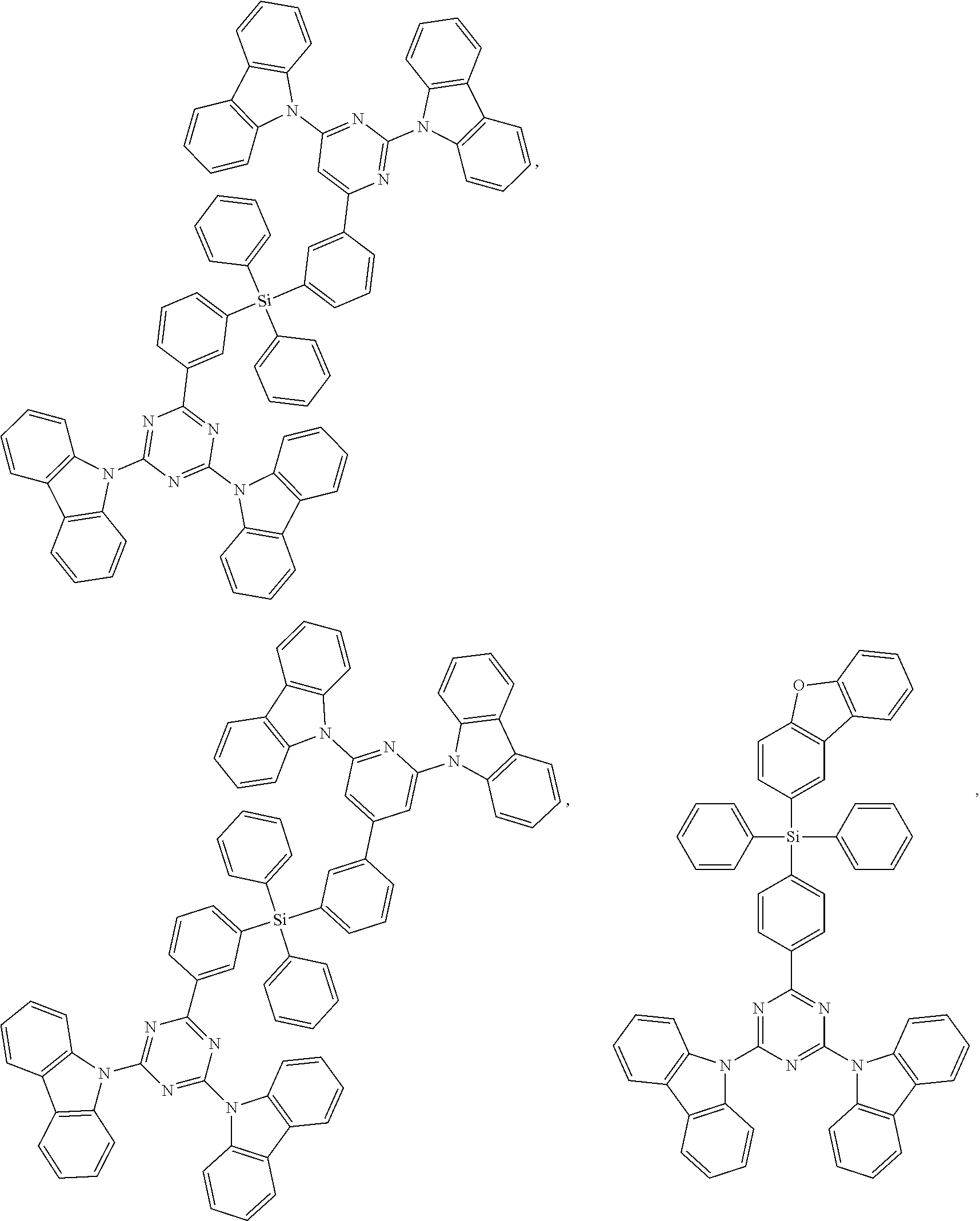


wherein the variables are the same as previously defined.


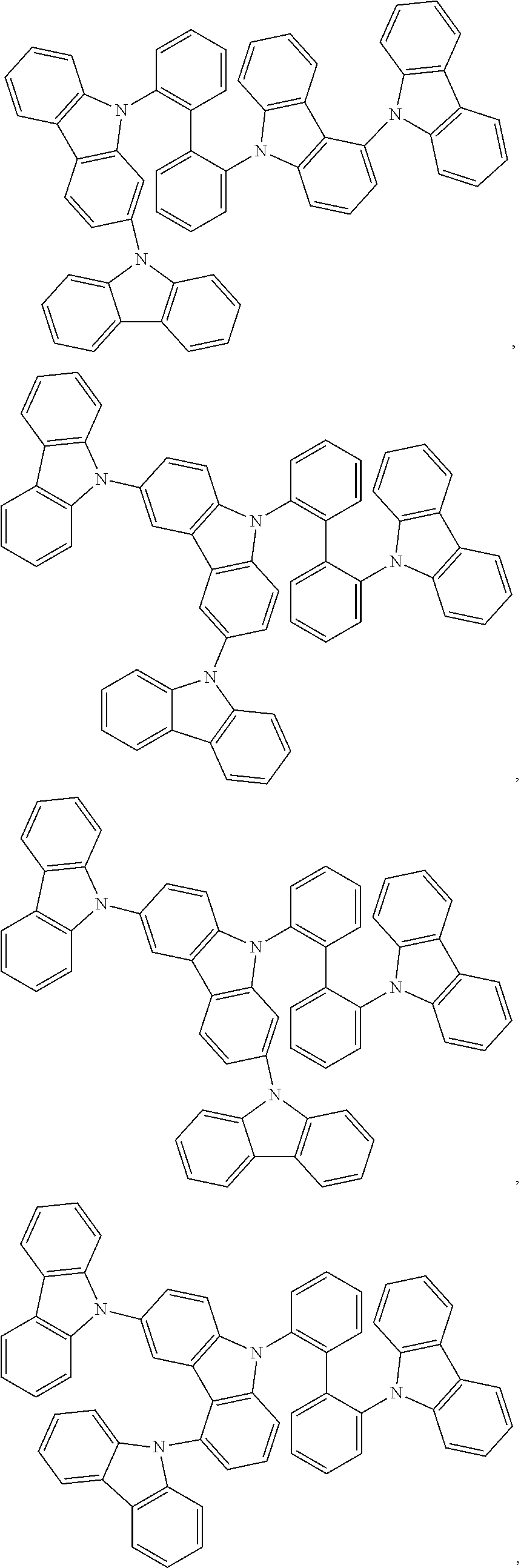


and combinations thereof.


b) HIL/HTL:


wherein k is an integer from 1 to 20; X101 to X108 is C (including CH) or N; Z101 is NAr1, O, or S; Ar1 has the same group defined above.
wherein Met is a metal, which can have an atomic weight greater than 40; (Y101-Y102) is a bidentate ligand, Y101 and Y102 are independently selected from C, N, O, P, and S; L101 is an ancillary ligand; k′ is an integer value from 1 to the maximum number of ligands that may be attached to the metal; and k′+k″ is the maximum number of ligands that may be attached to the metal.


c) EBL:
wherein Met is a metal; (Y103-Y104) is a bidentate ligand, Y103 and Y104 are independently selected from C, N, O, P, and S; L101 is an another ligand; k′ is an integer value from 1 to the maximum number of ligands that may be attached to the metal; and k′+k″ is the maximum number of ligands that may be attached to the metal.
wherein (O—N) is a bidentate ligand, having metal coordinated to atoms O and N.


wherein R101 is selected from the group consisting of hydrogen, deuterium, halogen, alkyl, cycloalkyl, heteroalkyl, heterocycloalkyl, arylalkyl, alkoxy, aryloxy, amino, silyl, alkenyl, cycloalkenyl, heteroalkenyl, alkynyl, aryl, heteroaryl, acyl, carboxylic acids, ether, ester, nitrile, isonitrile, sulfanyl, sulfinyl, sulfonyl, phosphino, and combinations thereof, and when it is aryl or heteroaryl, it has the similar definition as Ar's mentioned above. k is an integer from 0 to 20 or 1 to 20. X101 to X108 are independently selected from C (including CH) or N. Z101 and Z102 are independently selected from NR101, O, or S.


e) Additional Emitters:


f) HBL:

wherein k is an integer from 1 to 20; L101 is another ligand, k′ is an integer from 1 to 3.
g) ETL:

wherein R101 is selected from the group consisting of hydrogen, deuterium, halogen, alkyl, cycloalkyl, heteroalkyl, heterocycloalkyl, arylalkyl, alkoxy, aryloxy, amino, silyl, alkenyl, cycloalkenyl, heteroalkenyl, alkynyl, aryl, heteroaryl, acyl, carboxylic acids, ether, ester, nitrile, isonitrile, sulfanyl, sulfinyl, sulfonyl, phosphino, and combinations thereof, when it is aryl or heteroaryl, it has the similar definition as Ar's mentioned above. Ar1 to Ar3 has the similar definition as Ar's mentioned above. k is an integer from 1 to 20. X101 to X108 is selected from C (including CH) or N.

wherein (O—N) or (N—N) is a bidentate ligand, having metal coordinated to atoms O, N or N, N; L101 is another ligand; k′ is an integer value from 1 to the maximum number of ligands that may be attached to the metal.


h) Charge Generation Layer (CGL)


| TABLE 1 |
| Performance of devices with HH-3 |
| λ max | Voltage | EQE | LT90 | |||
| Device | Host 1 | Host 2 | (nm) | (relative) | (relative) | (relative) |
| Example 1 | EH-l | HH-3 | 469 | 1.08 | 1.05 | 1.77 |
| Example 2 | EH-2 | HH-3 | 468 | 1.05 | 0.90 | 2.84 |
| Example 3 | EH-3 | HH-3 | 467 | 1.11 | 0.94 | 1.13 |
| Example 4 | EH-4 | HH-3 | 468 | 1.11 | 0.87 | 2.16 |
| Example 5 | EH-5 | HH-3 | 467 | 1.03 | 0.89 | 1.80 |
| Example 6 | EH-6 | HH-3 | 468 | 1.03 | 1.00 | 2.17 |
| Example 7 | EH-7 | HH-3 | 468 | 1.27 | 0.96 | 1.12 |
| Example 8 | EH-8 | HH-3 | 469 | 1.22 | 0.98 | 1.27 |
| Example 9 | EH-9 | HH-3 | 468 | 1.03 | 0.97 | 2.97 |
| Compar- | Compar- | HH-3 | 468 | 1.00 | 1.00 | 1.00 |
| ison 1 | ison 1 | |||||
| TABLE 2 |
| Performance of devices with EH-9 |
| λ max | Voltage | EQE | LT90 | |||
| Device | Host 1 | Host 2 | (nm) | (relative) | (relative) | (relative) |
| Example 10 | EH-9 | HH-1 | 469 | 0.98 | 1.07 | 1.97 |
| Example 11 | EH-9 | HH-2 | 468 | 1.00 | 1.08 | 2.13 |
| Example 12 | EH-9 | HH-3 | 468 | 0.93 | 1.08 | 2.65 |
| Example 13 | EH-9 | HH-4 | 469 | 0.90 | 1.06 | 1.53 |
| Compar- | EH-9 | Compar- | 469 | 1.00 | 1.00 | 1.00 |
| ison 2 | ison 2 | |||||
Claims (19)


Priority Applications (4)
| Application Number | Priority Date | Filing Date | Title |
|---|---|---|---|
| US17/201,222 US11716899B2 (en) | 2018-11-28 | 2021-03-15 | Organic electroluminescent materials and devices |
| CN202110354370.5A CN113497210A (en) | 2020-04-06 | 2021-04-01 | Organic electroluminescent material and device |
| KR1020210044146A KR20210124922A (en) | 2020-04-06 | 2021-04-05 | Organic electroluminescent materials and devices |
| US18/353,347 US20230363254A1 (en) | 2018-11-28 | 2023-07-17 | Organic electroluminescent materials and devices |
Applications Claiming Priority (5)
| Application Number | Priority Date | Filing Date | Title |
|---|---|---|---|
| US201862772403P | 2018-11-28 | 2018-11-28 | |
| US16/683,507 US11515489B2 (en) | 2018-11-28 | 2019-11-14 | Host materials for electroluminescent devices |
| US16/841,182 US11672165B2 (en) | 2018-11-28 | 2020-04-06 | Organic electroluminescent materials and devices |
| US202063036764P | 2020-06-09 | 2020-06-09 | |
| US17/201,222 US11716899B2 (en) | 2018-11-28 | 2021-03-15 | Organic electroluminescent materials and devices |
Related Parent Applications (1)
| Application Number | Title | Priority Date | Filing Date |
|---|---|---|---|
| US16/841,182 Continuation-In-Part US11672165B2 (en) | 2018-11-28 | 2020-04-06 | Organic electroluminescent materials and devices |
Related Child Applications (1)
| Application Number | Title | Priority Date | Filing Date |
|---|---|---|---|
| US18/353,347 Continuation US20230363254A1 (en) | 2018-11-28 | 2023-07-17 | Organic electroluminescent materials and devices |
Publications (2)
| Publication Number | Publication Date |
|---|---|
| US20210210700A1 US20210210700A1 (en) | 2021-07-08 |
| US11716899B2 true US11716899B2 (en) | 2023-08-01 |
Family
ID=76654473
Family Applications (2)
| Application Number | Title | Priority Date | Filing Date |
|---|---|---|---|
| US17/201,222 Active 2040-02-02 US11716899B2 (en) | 2018-11-28 | 2021-03-15 | Organic electroluminescent materials and devices |
| US18/353,347 Pending US20230363254A1 (en) | 2018-11-28 | 2023-07-17 | Organic electroluminescent materials and devices |
Family Applications After (1)
| Application Number | Title | Priority Date | Filing Date |
|---|---|---|---|
| US18/353,347 Pending US20230363254A1 (en) | 2018-11-28 | 2023-07-17 | Organic electroluminescent materials and devices |
Country Status (1)
| Country | Link |
|---|---|
| US (2) | US11716899B2 (en) |
Families Citing this family (7)
| Publication number | Priority date | Publication date | Assignee | Title |
|---|---|---|---|---|
| EP3232485A1 (en) * | 2012-07-10 | 2017-10-18 | UDC Ireland Limited | Benzimidazo[1,2-a]benzimidazole derivatives for electronic applications |
| US11758807B2 (en) * | 2019-02-22 | 2023-09-12 | Universal Display Corporation | Organic electroluminescent materials and devices |
| EP4120381A1 (en) * | 2021-07-16 | 2023-01-18 | Samsung Electronics Co., Ltd. | Organic light-emitting device |
| CN117343078A (en) | 2021-11-25 | 2024-01-05 | 北京夏禾科技有限公司 | Organic electroluminescent material and device |
| WO2023170880A1 (en) * | 2022-03-10 | 2023-09-14 | 国立大学法人京都大学 | Dicarbazolyl benzene compound and organic electroluminescent device |
| US20230363269A1 (en) * | 2022-05-04 | 2023-11-09 | Samsung Electronics Co., Ltd. | Organic light-emitting device and electronic apparatus including the same |
| TW202402758A (en) * | 2022-05-25 | 2024-01-16 | 日商日鐵化學材料股份有限公司 | Material for photoelectric conversion element for imaging, and photoelectric conversion element for imaging using same |
Citations (134)
| Publication number | Priority date | Publication date | Assignee | Title |
|---|---|---|---|---|
| US4769292A (en) | 1987-03-02 | 1988-09-06 | Eastman Kodak Company | Electroluminescent device with modified thin film luminescent zone |
| US5061569A (en) | 1990-07-26 | 1991-10-29 | Eastman Kodak Company | Electroluminescent device with organic electroluminescent medium |
| US5247190A (en) | 1989-04-20 | 1993-09-21 | Cambridge Research And Innovation Limited | Electroluminescent devices |
| EP0650955A1 (en) | 1993-11-01 | 1995-05-03 | Hodogaya Chemical Co., Ltd. | Amine compound and electro-luminescence device comprising same |
| US5703436A (en) | 1994-12-13 | 1997-12-30 | The Trustees Of Princeton University | Transparent contacts for organic devices |
| US5707745A (en) | 1994-12-13 | 1998-01-13 | The Trustees Of Princeton University | Multicolor organic light emitting devices |
| US5834893A (en) | 1996-12-23 | 1998-11-10 | The Trustees Of Princeton University | High efficiency organic light emitting devices with light directing structures |
| US5844363A (en) | 1997-01-23 | 1998-12-01 | The Trustees Of Princeton Univ. | Vacuum deposited, non-polymeric flexible organic light emitting devices |
| US6013982A (en) | 1996-12-23 | 2000-01-11 | The Trustees Of Princeton University | Multicolor display devices |
| US6087196A (en) | 1998-01-30 | 2000-07-11 | The Trustees Of Princeton University | Fabrication of organic semiconductor devices using ink jet printing |
| US6091195A (en) | 1997-02-03 | 2000-07-18 | The Trustees Of Princeton University | Displays having mesa pixel configuration |
| US6097147A (en) | 1998-09-14 | 2000-08-01 | The Trustees Of Princeton University | Structure for high efficiency electroluminescent device |
| WO2001039234A2 (en) | 1999-11-24 | 2001-05-31 | The Trustees Of Princeton University | Organic light emitting diode having a blue phosphorescent molecule as an emitter |
| US6294398B1 (en) | 1999-11-23 | 2001-09-25 | The Trustees Of Princeton University | Method for patterning devices |
| US6303238B1 (en) | 1997-12-01 | 2001-10-16 | The Trustees Of Princeton University | OLEDs doped with phosphorescent compounds |
| US6337102B1 (en) | 1997-11-17 | 2002-01-08 | The Trustees Of Princeton University | Low pressure vapor phase deposition of organic thin films |
| WO2002002714A2 (en) | 2000-06-30 | 2002-01-10 | E.I. Du Pont De Nemours And Company | Electroluminescent iridium compounds with fluorinated phenylpyridines, phenylpyrimidines, and phenylquinolines and devices made with such compounds |
| WO2002015654A1 (en) | 2000-08-04 | 2002-02-21 | Toray Engineering Co., Ltd. | Mounting method and mounting device |
| US20020034656A1 (en) | 1998-09-14 | 2002-03-21 | Thompson Mark E. | Organometallic complexes as phosphorescent emitters in organic LEDs |
| US20020134984A1 (en) | 2001-02-01 | 2002-09-26 | Fuji Photo Film Co., Ltd. | Transition metal complex and light-emitting device |
| US20020158242A1 (en) | 1999-12-31 | 2002-10-31 | Se-Hwan Son | Electronic device comprising organic compound having p-type semiconducting characteristics |
| US6528187B1 (en) | 1998-09-08 | 2003-03-04 | Fuji Photo Film Co., Ltd. | Material for luminescence element and luminescence element using the same |
| WO2003040257A1 (en) | 2001-11-07 | 2003-05-15 | E. I. Du Pont De Nemours And Company | Electroluminescent platinum compounds and devices made with such compounds |
| WO2003060956A2 (en) | 2002-01-18 | 2003-07-24 | Lg Chem, Ltd. | New material for transporting electrons and organic electroluminescent display using the same |
| US20030138657A1 (en) | 2000-12-07 | 2003-07-24 | Canon Kabushiki Kaisha | Deuterated semi-conducting organic compounds used for opto-electronic devices |
| US20030152802A1 (en) | 2001-06-19 | 2003-08-14 | Akira Tsuboyama | Metal coordination compound and organic liminescence device |
| US20030162053A1 (en) | 1996-06-25 | 2003-08-28 | Marks Tobin J. | Organic light - emitting diodes and methods for assembly and enhanced charge injection |
| US20030175553A1 (en) | 2001-12-28 | 2003-09-18 | Thompson Mark E. | White light emitting oleds from combined monomer and aggregate emission |
| US20030230980A1 (en) | 2002-06-18 | 2003-12-18 | Forrest Stephen R | Very low voltage, high efficiency phosphorescent oled in a p-i-n structure |
| US6687266B1 (en) | 2002-11-08 | 2004-02-03 | Universal Display Corporation | Organic light emitting materials and devices |
| US20040036077A1 (en) | 2002-08-22 | 2004-02-26 | Fuji Photo Film Co., Ltd. | Light emitting element |
| US20040137268A1 (en) | 2002-12-27 | 2004-07-15 | Fuji Photo Film Co., Ltd. | Organic electroluminescent device |
| US20040137267A1 (en) | 2002-12-27 | 2004-07-15 | Fuji Photo Film Co., Ltd. | Organic electroluminescent device |
| US20040174116A1 (en) | 2001-08-20 | 2004-09-09 | Lu Min-Hao Michael | Transparent electrodes |
| WO2004093207A2 (en) | 2003-04-15 | 2004-10-28 | Covion Organic Semiconductors Gmbh | Mixtures of matrix materials and organic semiconductors capable of emission, use of the same and electronic components containing said mixtures |
| WO2004107822A1 (en) | 2003-05-29 | 2004-12-09 | Nippon Steel Chemical Co., Ltd. | Organic electroluminescent element |
| US6835469B2 (en) | 2001-10-17 | 2004-12-28 | The University Of Southern California | Phosphorescent compounds and devices comprising the same |
| JP2005011610A (en) | 2003-06-18 | 2005-01-13 | Nippon Steel Chem Co Ltd | Organic electroluminescent element |
| US20050025993A1 (en) | 2003-07-25 | 2005-02-03 | Thompson Mark E. | Materials and structures for enhancing the performance of organic light emitting devices |
| WO2005014551A1 (en) | 2003-08-07 | 2005-02-17 | Nippon Steel Chemical Co., Ltd. | Aluminum chelate compelx for organic el material |
| WO2005019373A2 (en) | 2003-08-19 | 2005-03-03 | Basf Aktiengesellschaft | Transition metal complexes comprising carbene ligands serving as emitters for organic light-emitting diodes (oled's) |
| WO2005030900A1 (en) | 2003-09-25 | 2005-04-07 | Nippon Steel Chemical Co., Ltd. | Organic electroluminescent device |
| US20050112407A1 (en) | 2003-11-21 | 2005-05-26 | Fuji Photo Film Co., Ltd. | Organic electroluminescent device |
| US6921915B2 (en) | 2001-03-08 | 2005-07-26 | Canon Kabushiki Kaisha | Metal coordination compound, luminescence device and display apparatus |
| WO2005089025A1 (en) | 2004-03-15 | 2005-09-22 | Nippon Steel Chemical Co., Ltd. | Organic electroluminescent device |
| US20050238919A1 (en) | 2004-04-23 | 2005-10-27 | Fuji Photo Film Co., Ltd. | Organic electroluminescent device |
| US20050244673A1 (en) | 2002-08-27 | 2005-11-03 | Fujitsu Limited | Organometallic complex, organic EL element and organic EL display |
| US20050260441A1 (en) | 2004-05-18 | 2005-11-24 | Thompson Mark E | Luminescent compounds with carbene ligands |
| US20050260449A1 (en) | 2004-05-18 | 2005-11-24 | Robert Walters | Complexes with tridentate ligands |
| WO2005123873A1 (en) | 2004-06-17 | 2005-12-29 | Konica Minolta Holdings, Inc. | Organic electroluminescent device material, organic electroluminescent device, display and illuminating device |
| US20060008670A1 (en) | 2004-07-06 | 2006-01-12 | Chun Lin | Organic light emitting materials and devices |
| WO2006009024A1 (en) | 2004-07-23 | 2006-01-26 | Konica Minolta Holdings, Inc. | Organic electroluminescent device, display and illuminating device |
| WO2006056418A2 (en) | 2004-11-25 | 2006-06-01 | Basf Aktiengesellschaft | Use of transition metal carbene complexes in organic light-emitting diodes (oleds) |
| WO2006072002A2 (en) | 2004-12-30 | 2006-07-06 | E.I. Dupont De Nemours And Company | Organometallic complexes |
| US7087321B2 (en) | 2003-04-22 | 2006-08-08 | Universal Display Corporation | Organic light emitting devices having reduced pixel shrinkage |
| WO2006082742A1 (en) | 2005-02-04 | 2006-08-10 | Konica Minolta Holdings, Inc. | Organic electroluminescent device material, organic electroluminescent device, display and illuminating device |
| US7090928B2 (en) | 2003-04-01 | 2006-08-15 | The University Of Southern California | Binuclear compounds |
| US20060202194A1 (en) | 2005-03-08 | 2006-09-14 | Jeong Hyun C | Red phosphorescene compounds and organic electroluminescence device using the same |
| WO2006098120A1 (en) | 2005-03-16 | 2006-09-21 | Konica Minolta Holdings, Inc. | Organic electroluminescent device material and organic electroluminescent device |
| WO2006100298A1 (en) | 2005-03-24 | 2006-09-28 | Basf Aktiengesellschaft | Use of compounds containing aromatic or heteroaromatic rings linked via carbonyl group-containing groups, for use as matrix materials in organic light-emitting diodes |
| WO2006103874A1 (en) | 2005-03-29 | 2006-10-05 | Konica Minolta Holdings, Inc. | Organic electroluminescent device material, organic electroluminescent device, display and illuminating device |
| US20060240279A1 (en) | 2005-04-21 | 2006-10-26 | Vadim Adamovich | Non-blocked phosphorescent OLEDs |
| WO2006114966A1 (en) | 2005-04-18 | 2006-11-02 | Konica Minolta Holdings, Inc. | Organic electroluminescent device, display and illuminating device |
| US20060251923A1 (en) | 2005-05-06 | 2006-11-09 | Chun Lin | Stability OLED materials and devices |
| EP1725079A1 (en) | 2004-03-11 | 2006-11-22 | Mitsubishi Chemical Corporation | Composition for charge-transporting film and ion compound, charge-transporting film and organic electroluminescent device using same, and method for manufacturing organic electroluminescent device and method for producing charge-transporting film |
| US20060263635A1 (en) | 2005-05-06 | 2006-11-23 | Fuji Photo Film Co., Ltd. | Organic electroluminescent device |
| WO2006132173A1 (en) | 2005-06-07 | 2006-12-14 | Nippon Steel Chemical Co., Ltd. | Organic metal complex and organic electroluminescent device using same |
| US20060280965A1 (en) | 2005-05-31 | 2006-12-14 | Raymond Kwong | Triphenylene hosts in phosphorescent light emitting diodes |
| US7154114B2 (en) | 2004-05-18 | 2006-12-26 | Universal Display Corporation | Cyclometallated iridium carbene complexes for use as hosts |
| WO2007002683A2 (en) | 2005-06-27 | 2007-01-04 | E. I. Du Pont De Nemours And Company | Electrically conductive polymer compositions |
| WO2007004380A1 (en) | 2005-07-01 | 2007-01-11 | Konica Minolta Holdings, Inc. | Organic electroluminescent element material, organic electroluminescent element, display device, and lighting equipment |
| JP2007123392A (en) | 2005-10-26 | 2007-05-17 | Konica Minolta Holdings Inc | Organic electroluminescence device, display device and lighting device |
| WO2007063796A1 (en) | 2005-12-01 | 2007-06-07 | Nippon Steel Chemical Co., Ltd. | Organic electroluminescent device |
| WO2007063754A1 (en) | 2005-12-01 | 2007-06-07 | Nippon Steel Chemical Co., Ltd. | Compound for organic electroluminescent element and organic electroluminescent element |
| US7250226B2 (en) | 2001-08-31 | 2007-07-31 | Nippon Hoso Kyokai | Phosphorescent compound, a phosphorescent composition and an organic light-emitting device |
| US20070190359A1 (en) | 2006-02-10 | 2007-08-16 | Knowles David B | Metal complexes of cyclometallated imidazo[1,2-ƒ]phenanthridine and diimidazo[1,2-a:1',2'-c]quinazoline ligands and isoelectronic and benzannulated analogs thereof |
| JP2007254297A (en) | 2006-03-20 | 2007-10-04 | Nippon Steel Chem Co Ltd | Compound of light-emitting layer and organic electroluminescent device |
| US20070278938A1 (en) | 2006-04-26 | 2007-12-06 | Idemitsu Kosan Co., Ltd. | Aromatic amine derivative and electroluminescence device using the same |
| US20080015355A1 (en) | 2004-06-28 | 2008-01-17 | Thomas Schafer | Electroluminescent Metal Complexes With Triazoles And Benzotriazoles |
| US7332232B2 (en) | 2004-02-03 | 2008-02-19 | Universal Display Corporation | OLEDs utilizing multidentate ligand systems |
| US7338722B2 (en) | 2003-03-24 | 2008-03-04 | The University Of Southern California | Phenyl and fluorenyl substituted phenyl-pyrazole complexes of Ir |
| JP2008074939A (en) | 2006-09-21 | 2008-04-03 | Konica Minolta Holdings Inc | Organic electroluminescence element material, organic electroluminescence element, display device and illumination device |
| US20080106190A1 (en) | 2006-08-23 | 2008-05-08 | Idemitsu Kosan Co., Ltd. | Aromatic amine derivatives and organic electroluminescent device using same |
| WO2008056746A1 (en) | 2006-11-09 | 2008-05-15 | Nippon Steel Chemical Co., Ltd. | Compound for organic electroluminescent device and organic electroluminescent device |
| US20080124572A1 (en) | 2006-11-24 | 2008-05-29 | Idemitsu Kosan Co., Ltd. | Aromatic amine derivative and organic electroluminescence device using the same |
| US7393599B2 (en) | 2004-05-18 | 2008-07-01 | The University Of Southern California | Luminescent compounds with carbene ligands |
| US7396598B2 (en) | 2001-06-20 | 2008-07-08 | Showa Denko K.K. | Light emitting material and organic light-emitting device |
| WO2008101842A1 (en) | 2007-02-23 | 2008-08-28 | Basf Se | Electroluminescent metal complexes with benzotriazoles |
| US20080220265A1 (en) | 2006-12-08 | 2008-09-11 | Universal Display Corporation | Cross-linkable Iridium Complexes and Organic Light-Emitting Devices Using the Same |
| US7431968B1 (en) | 2001-09-04 | 2008-10-07 | The Trustees Of Princeton University | Process and apparatus for organic vapor jet deposition |
| US7445855B2 (en) | 2004-05-18 | 2008-11-04 | The University Of Southern California | Cationic metal-carbene complexes |
| WO2008132085A1 (en) | 2007-04-26 | 2008-11-06 | Basf Se | Silanes containing phenothiazine-s-oxide or phenothiazine-s,s-dioxide groups and the use thereof in oleds |
| US20080297033A1 (en) | 2006-02-10 | 2008-12-04 | Knowles David B | Blue phosphorescent imidazophenanthridine materials |
| WO2009000673A2 (en) | 2007-06-22 | 2008-12-31 | Basf Se | Light emitting cu(i) complexes |
| WO2009003898A1 (en) | 2007-07-05 | 2009-01-08 | Basf Se | Organic light-emitting diodes containing carbene transition metal complex emitters and at least one compound selected from disilylcarbazoles, disilyldibenzofurans, disilyldibenzothiophenes, disilyldibenzophospholes, disilyldibenzothiophene s-oxides and disilyldibenzothiophene s,s-dioxides |
| US20090008605A1 (en) | 2007-07-07 | 2009-01-08 | Idemitsu Kosan Co., Ltd. | Naphthalene derivative, material for organic electroluminescence device, and organic electroluminescence device using the same |
| US20090009065A1 (en) | 2007-07-07 | 2009-01-08 | Idemitsu Kosan Co., Ltd. | Organic electroluminescence device and material for organic electroluminescence device |
| US20090017330A1 (en) | 2007-07-10 | 2009-01-15 | Idemitsu Kosan Co., Ltd. | Material for organic electroluminescence device and organic electroluminescence device utilizing the same |
| WO2009008311A1 (en) | 2007-07-07 | 2009-01-15 | Idemitsu Kosan Co., Ltd. | Chrysene derivative and organic electroluminescent device using the same |
| US20090030202A1 (en) | 2007-07-10 | 2009-01-29 | Idemitsu Kosan Co., Ltd. | Material for organic electroluminescent element and organic electroluminescent element employing the same |
| WO2009018009A1 (en) | 2007-07-27 | 2009-02-05 | E. I. Du Pont De Nemours And Company | Aqueous dispersions of electrically conducting polymers containing inorganic nanoparticles |
| US20090039776A1 (en) | 2007-08-09 | 2009-02-12 | Canon Kabushiki Kaisha | Organometallic complex and organic light-emitting element using same |
| WO2009021126A2 (en) | 2007-08-08 | 2009-02-12 | Universal Display Corporation | Benzo-fused thiophene or benzo-fused furan compounds comprising a triphenylene group |
| US20090045730A1 (en) | 2007-07-07 | 2009-02-19 | Idemitsu Kosan Co., Ltd. | Organic electroluminescence device and material for organic electroluminescence device |
| US20090045731A1 (en) | 2007-07-07 | 2009-02-19 | Idemitsu Kosan Co., Ltd. | Organic electroluminescence device and material for organic electroluminescence device |
| EP2034538A1 (en) | 2006-06-02 | 2009-03-11 | Idemitsu Kosan Co., Ltd. | Material for organic electroluminescence element, and organic electroluminescence element using the material |
| WO2009050290A1 (en) | 2007-10-17 | 2009-04-23 | Basf Se | Transition metal complexes having bridged carbene ligands and the use thereof in oleds |
| US20090101870A1 (en) | 2007-10-22 | 2009-04-23 | E. I. Du Pont De Nemours And Company | Electron transport bi-layers and devices made with such bi-layers |
| US20090108737A1 (en) | 2006-12-08 | 2009-04-30 | Raymond Kwong | Light-emitting organometallic complexes |
| US20090115316A1 (en) | 2007-11-02 | 2009-05-07 | Shiying Zheng | Organic electroluminescent device having an azatriphenylene derivative |
| US7534505B2 (en) | 2004-05-18 | 2009-05-19 | The University Of Southern California | Organometallic compounds for use in electroluminescent devices |
| WO2009063833A1 (en) | 2007-11-15 | 2009-05-22 | Idemitsu Kosan Co., Ltd. | Benzochrysene derivative and organic electroluminescent device using the same |
| WO2009062578A1 (en) | 2007-11-12 | 2009-05-22 | Merck Patent Gmbh | Organic electroluminescent devices comprising azomethine-metal complexes |
| WO2009066778A1 (en) | 2007-11-22 | 2009-05-28 | Idemitsu Kosan Co., Ltd. | Organic el element and solution containing organic el material |
| WO2009066779A1 (en) | 2007-11-22 | 2009-05-28 | Idemitsu Kosan Co., Ltd. | Organic el element |
| US20090165846A1 (en) | 2005-09-07 | 2009-07-02 | Universitaet Braunschweig | Triplet emitter having condensed five-membered rings |
| US20090167162A1 (en) | 2007-12-28 | 2009-07-02 | Universal Display Corporation | Dibenzothiophene-containing materials in phosphorescent light emitting diodes |
| WO2009086028A2 (en) | 2007-12-28 | 2009-07-09 | Universal Display Corporation | Carbazole-containing materials in phosphorescent light emitting diodes |
| US20090179554A1 (en) | 2006-05-11 | 2009-07-16 | Hitoshi Kuma | Organic electroluminescent device |
| WO2009100991A1 (en) | 2008-02-12 | 2009-08-20 | Basf Se | Electroluminescent metal complexes with dibenzo[f,h]quinoxalines |
| WO2013165192A1 (en) | 2012-05-02 | 2013-11-07 | Rohm And Haas Electronic Materials Korea Ltd. | Novel organic electroluminescence compounds and organic electroluminescence device containing the same |
| KR20150058080A (en) | 2013-11-20 | 2015-05-28 | 주식회사 동진쎄미켐 | Novel electroluminescent compound and organic electroluminescent device comprising same |
| US20170012207A1 (en) | 2015-07-08 | 2017-01-12 | Semiconductor Energy Laboratory Co., Ltd. | Light-Emitting Element, Display Device, Electronic Device, and Lighting Device |
| US20180254426A1 (en) | 2015-03-30 | 2018-09-06 | Nippon Steel & Sumikin Chemical Co., Ltd. | Organic electroluminescent element |
| US20190036055A1 (en) * | 2017-07-26 | 2019-01-31 | Universal Display Corporation | Organic electroluminescent materials and devices |
| US20190058144A1 (en) | 2017-07-31 | 2019-02-21 | Samsung Electronics Co., Ltd. | Organic light-emitting device |
| US20190280215A1 (en) | 2018-03-08 | 2019-09-12 | Samsung Display Co., Ltd. | Organic light-emitting device |
| US20200168811A1 (en) * | 2018-11-28 | 2020-05-28 | Universal Display Corporation | Host materials for electroluminescent devices |
| US20200168819A1 (en) * | 2018-11-26 | 2020-05-28 | Samsung Display Co., Ltd. | Heterocyclic compound and organic light-emitting device including the same |
| US20200270262A1 (en) | 2019-02-22 | 2020-08-27 | Universal Display Corporation | Organic Electroluminescent Materials and Devices |
| US20210057654A1 (en) | 2018-11-28 | 2021-02-25 | Universal Display Corporation | Host materials for electroluminescent devices |
| US20210359227A1 (en) | 2020-05-18 | 2021-11-18 | Samsung Display Co., Ltd. | Organic electroluminescence device and organometallic compound for organic electroluminescence device |
| US20220020939A1 (en) | 2020-07-17 | 2022-01-20 | Samsung Display Co., Ltd. | Light-emitting device and electronic apparatus including the light-emitting device |
| US20220109121A1 (en) | 2020-10-07 | 2022-04-07 | Samsung Display Co., Ltd. | Organic electroluminescence device |
Family Cites Families (1)
| Publication number | Priority date | Publication date | Assignee | Title |
|---|---|---|---|---|
| EP3141550B1 (en) * | 2015-09-09 | 2020-03-18 | Samsung Electronics Co., Ltd. | Condensed cyclic compound and organic light-emitting device including the same |
-
2021
- 2021-03-15 US US17/201,222 patent/US11716899B2/en active Active
-
2023
- 2023-07-17 US US18/353,347 patent/US20230363254A1/en active Pending
Patent Citations (138)
| Publication number | Priority date | Publication date | Assignee | Title |
|---|---|---|---|---|
| US4769292A (en) | 1987-03-02 | 1988-09-06 | Eastman Kodak Company | Electroluminescent device with modified thin film luminescent zone |
| US5247190A (en) | 1989-04-20 | 1993-09-21 | Cambridge Research And Innovation Limited | Electroluminescent devices |
| US5061569A (en) | 1990-07-26 | 1991-10-29 | Eastman Kodak Company | Electroluminescent device with organic electroluminescent medium |
| EP0650955A1 (en) | 1993-11-01 | 1995-05-03 | Hodogaya Chemical Co., Ltd. | Amine compound and electro-luminescence device comprising same |
| US5703436A (en) | 1994-12-13 | 1997-12-30 | The Trustees Of Princeton University | Transparent contacts for organic devices |
| US5707745A (en) | 1994-12-13 | 1998-01-13 | The Trustees Of Princeton University | Multicolor organic light emitting devices |
| US20030162053A1 (en) | 1996-06-25 | 2003-08-28 | Marks Tobin J. | Organic light - emitting diodes and methods for assembly and enhanced charge injection |
| US5834893A (en) | 1996-12-23 | 1998-11-10 | The Trustees Of Princeton University | High efficiency organic light emitting devices with light directing structures |
| US6013982A (en) | 1996-12-23 | 2000-01-11 | The Trustees Of Princeton University | Multicolor display devices |
| US5844363A (en) | 1997-01-23 | 1998-12-01 | The Trustees Of Princeton Univ. | Vacuum deposited, non-polymeric flexible organic light emitting devices |
| US6091195A (en) | 1997-02-03 | 2000-07-18 | The Trustees Of Princeton University | Displays having mesa pixel configuration |
| US6337102B1 (en) | 1997-11-17 | 2002-01-08 | The Trustees Of Princeton University | Low pressure vapor phase deposition of organic thin films |
| US6303238B1 (en) | 1997-12-01 | 2001-10-16 | The Trustees Of Princeton University | OLEDs doped with phosphorescent compounds |
| US6087196A (en) | 1998-01-30 | 2000-07-11 | The Trustees Of Princeton University | Fabrication of organic semiconductor devices using ink jet printing |
| US6528187B1 (en) | 1998-09-08 | 2003-03-04 | Fuji Photo Film Co., Ltd. | Material for luminescence element and luminescence element using the same |
| US6097147A (en) | 1998-09-14 | 2000-08-01 | The Trustees Of Princeton University | Structure for high efficiency electroluminescent device |
| US20020034656A1 (en) | 1998-09-14 | 2002-03-21 | Thompson Mark E. | Organometallic complexes as phosphorescent emitters in organic LEDs |
| US6468819B1 (en) | 1999-11-23 | 2002-10-22 | The Trustees Of Princeton University | Method for patterning organic thin film devices using a die |
| US6294398B1 (en) | 1999-11-23 | 2001-09-25 | The Trustees Of Princeton University | Method for patterning devices |
| WO2001039234A2 (en) | 1999-11-24 | 2001-05-31 | The Trustees Of Princeton University | Organic light emitting diode having a blue phosphorescent molecule as an emitter |
| US20020158242A1 (en) | 1999-12-31 | 2002-10-31 | Se-Hwan Son | Electronic device comprising organic compound having p-type semiconducting characteristics |
| WO2002002714A2 (en) | 2000-06-30 | 2002-01-10 | E.I. Du Pont De Nemours And Company | Electroluminescent iridium compounds with fluorinated phenylpyridines, phenylpyrimidines, and phenylquinolines and devices made with such compounds |
| WO2002015654A1 (en) | 2000-08-04 | 2002-02-21 | Toray Engineering Co., Ltd. | Mounting method and mounting device |
| US20030138657A1 (en) | 2000-12-07 | 2003-07-24 | Canon Kabushiki Kaisha | Deuterated semi-conducting organic compounds used for opto-electronic devices |
| US20020134984A1 (en) | 2001-02-01 | 2002-09-26 | Fuji Photo Film Co., Ltd. | Transition metal complex and light-emitting device |
| US6921915B2 (en) | 2001-03-08 | 2005-07-26 | Canon Kabushiki Kaisha | Metal coordination compound, luminescence device and display apparatus |
| US20030152802A1 (en) | 2001-06-19 | 2003-08-14 | Akira Tsuboyama | Metal coordination compound and organic liminescence device |
| US7396598B2 (en) | 2001-06-20 | 2008-07-08 | Showa Denko K.K. | Light emitting material and organic light-emitting device |
| US20040174116A1 (en) | 2001-08-20 | 2004-09-09 | Lu Min-Hao Michael | Transparent electrodes |
| US7250226B2 (en) | 2001-08-31 | 2007-07-31 | Nippon Hoso Kyokai | Phosphorescent compound, a phosphorescent composition and an organic light-emitting device |
| US7431968B1 (en) | 2001-09-04 | 2008-10-07 | The Trustees Of Princeton University | Process and apparatus for organic vapor jet deposition |
| US6835469B2 (en) | 2001-10-17 | 2004-12-28 | The University Of Southern California | Phosphorescent compounds and devices comprising the same |
| WO2003040257A1 (en) | 2001-11-07 | 2003-05-15 | E. I. Du Pont De Nemours And Company | Electroluminescent platinum compounds and devices made with such compounds |
| US20030175553A1 (en) | 2001-12-28 | 2003-09-18 | Thompson Mark E. | White light emitting oleds from combined monomer and aggregate emission |
| WO2003060956A2 (en) | 2002-01-18 | 2003-07-24 | Lg Chem, Ltd. | New material for transporting electrons and organic electroluminescent display using the same |
| US20030230980A1 (en) | 2002-06-18 | 2003-12-18 | Forrest Stephen R | Very low voltage, high efficiency phosphorescent oled in a p-i-n structure |
| US20040036077A1 (en) | 2002-08-22 | 2004-02-26 | Fuji Photo Film Co., Ltd. | Light emitting element |
| US20050244673A1 (en) | 2002-08-27 | 2005-11-03 | Fujitsu Limited | Organometallic complex, organic EL element and organic EL display |
| US6687266B1 (en) | 2002-11-08 | 2004-02-03 | Universal Display Corporation | Organic light emitting materials and devices |
| US20040137268A1 (en) | 2002-12-27 | 2004-07-15 | Fuji Photo Film Co., Ltd. | Organic electroluminescent device |
| US20040137267A1 (en) | 2002-12-27 | 2004-07-15 | Fuji Photo Film Co., Ltd. | Organic electroluminescent device |
| US7338722B2 (en) | 2003-03-24 | 2008-03-04 | The University Of Southern California | Phenyl and fluorenyl substituted phenyl-pyrazole complexes of Ir |
| US7090928B2 (en) | 2003-04-01 | 2006-08-15 | The University Of Southern California | Binuclear compounds |
| WO2004093207A2 (en) | 2003-04-15 | 2004-10-28 | Covion Organic Semiconductors Gmbh | Mixtures of matrix materials and organic semiconductors capable of emission, use of the same and electronic components containing said mixtures |
| US7087321B2 (en) | 2003-04-22 | 2006-08-08 | Universal Display Corporation | Organic light emitting devices having reduced pixel shrinkage |
| WO2004107822A1 (en) | 2003-05-29 | 2004-12-09 | Nippon Steel Chemical Co., Ltd. | Organic electroluminescent element |
| JP2005011610A (en) | 2003-06-18 | 2005-01-13 | Nippon Steel Chem Co Ltd | Organic electroluminescent element |
| US20050025993A1 (en) | 2003-07-25 | 2005-02-03 | Thompson Mark E. | Materials and structures for enhancing the performance of organic light emitting devices |
| WO2005014551A1 (en) | 2003-08-07 | 2005-02-17 | Nippon Steel Chemical Co., Ltd. | Aluminum chelate compelx for organic el material |
| WO2005019373A2 (en) | 2003-08-19 | 2005-03-03 | Basf Aktiengesellschaft | Transition metal complexes comprising carbene ligands serving as emitters for organic light-emitting diodes (oled's) |
| WO2005030900A1 (en) | 2003-09-25 | 2005-04-07 | Nippon Steel Chemical Co., Ltd. | Organic electroluminescent device |
| US20050112407A1 (en) | 2003-11-21 | 2005-05-26 | Fuji Photo Film Co., Ltd. | Organic electroluminescent device |
| US7332232B2 (en) | 2004-02-03 | 2008-02-19 | Universal Display Corporation | OLEDs utilizing multidentate ligand systems |
| EP1725079A1 (en) | 2004-03-11 | 2006-11-22 | Mitsubishi Chemical Corporation | Composition for charge-transporting film and ion compound, charge-transporting film and organic electroluminescent device using same, and method for manufacturing organic electroluminescent device and method for producing charge-transporting film |
| WO2005089025A1 (en) | 2004-03-15 | 2005-09-22 | Nippon Steel Chemical Co., Ltd. | Organic electroluminescent device |
| US20050238919A1 (en) | 2004-04-23 | 2005-10-27 | Fuji Photo Film Co., Ltd. | Organic electroluminescent device |
| US7393599B2 (en) | 2004-05-18 | 2008-07-01 | The University Of Southern California | Luminescent compounds with carbene ligands |
| US7279704B2 (en) | 2004-05-18 | 2007-10-09 | The University Of Southern California | Complexes with tridentate ligands |
| US7534505B2 (en) | 2004-05-18 | 2009-05-19 | The University Of Southern California | Organometallic compounds for use in electroluminescent devices |
| US20050260441A1 (en) | 2004-05-18 | 2005-11-24 | Thompson Mark E | Luminescent compounds with carbene ligands |
| US20050260449A1 (en) | 2004-05-18 | 2005-11-24 | Robert Walters | Complexes with tridentate ligands |
| US7445855B2 (en) | 2004-05-18 | 2008-11-04 | The University Of Southern California | Cationic metal-carbene complexes |
| US7154114B2 (en) | 2004-05-18 | 2006-12-26 | Universal Display Corporation | Cyclometallated iridium carbene complexes for use as hosts |
| WO2005123873A1 (en) | 2004-06-17 | 2005-12-29 | Konica Minolta Holdings, Inc. | Organic electroluminescent device material, organic electroluminescent device, display and illuminating device |
| US20080015355A1 (en) | 2004-06-28 | 2008-01-17 | Thomas Schafer | Electroluminescent Metal Complexes With Triazoles And Benzotriazoles |
| US20060008670A1 (en) | 2004-07-06 | 2006-01-12 | Chun Lin | Organic light emitting materials and devices |
| WO2006009024A1 (en) | 2004-07-23 | 2006-01-26 | Konica Minolta Holdings, Inc. | Organic electroluminescent device, display and illuminating device |
| US20080018221A1 (en) | 2004-11-25 | 2008-01-24 | Basf Aktiengesellschaft | Use Of Transition Metal Carbene Complexes In Organic Light-Emitting Diodes (Oleds) |
| WO2006056418A2 (en) | 2004-11-25 | 2006-06-01 | Basf Aktiengesellschaft | Use of transition metal carbene complexes in organic light-emitting diodes (oleds) |
| WO2006072002A2 (en) | 2004-12-30 | 2006-07-06 | E.I. Dupont De Nemours And Company | Organometallic complexes |
| WO2006082742A1 (en) | 2005-02-04 | 2006-08-10 | Konica Minolta Holdings, Inc. | Organic electroluminescent device material, organic electroluminescent device, display and illuminating device |
| US20060202194A1 (en) | 2005-03-08 | 2006-09-14 | Jeong Hyun C | Red phosphorescene compounds and organic electroluminescence device using the same |
| WO2006098120A1 (en) | 2005-03-16 | 2006-09-21 | Konica Minolta Holdings, Inc. | Organic electroluminescent device material and organic electroluminescent device |
| WO2006100298A1 (en) | 2005-03-24 | 2006-09-28 | Basf Aktiengesellschaft | Use of compounds containing aromatic or heteroaromatic rings linked via carbonyl group-containing groups, for use as matrix materials in organic light-emitting diodes |
| WO2006103874A1 (en) | 2005-03-29 | 2006-10-05 | Konica Minolta Holdings, Inc. | Organic electroluminescent device material, organic electroluminescent device, display and illuminating device |
| WO2006114966A1 (en) | 2005-04-18 | 2006-11-02 | Konica Minolta Holdings, Inc. | Organic electroluminescent device, display and illuminating device |
| US20060240279A1 (en) | 2005-04-21 | 2006-10-26 | Vadim Adamovich | Non-blocked phosphorescent OLEDs |
| US20060251923A1 (en) | 2005-05-06 | 2006-11-09 | Chun Lin | Stability OLED materials and devices |
| US20060263635A1 (en) | 2005-05-06 | 2006-11-23 | Fuji Photo Film Co., Ltd. | Organic electroluminescent device |
| US20060280965A1 (en) | 2005-05-31 | 2006-12-14 | Raymond Kwong | Triphenylene hosts in phosphorescent light emitting diodes |
| WO2006132173A1 (en) | 2005-06-07 | 2006-12-14 | Nippon Steel Chemical Co., Ltd. | Organic metal complex and organic electroluminescent device using same |
| WO2007002683A2 (en) | 2005-06-27 | 2007-01-04 | E. I. Du Pont De Nemours And Company | Electrically conductive polymer compositions |
| WO2007004380A1 (en) | 2005-07-01 | 2007-01-11 | Konica Minolta Holdings, Inc. | Organic electroluminescent element material, organic electroluminescent element, display device, and lighting equipment |
| US20090165846A1 (en) | 2005-09-07 | 2009-07-02 | Universitaet Braunschweig | Triplet emitter having condensed five-membered rings |
| JP2007123392A (en) | 2005-10-26 | 2007-05-17 | Konica Minolta Holdings Inc | Organic electroluminescence device, display device and lighting device |
| WO2007063754A1 (en) | 2005-12-01 | 2007-06-07 | Nippon Steel Chemical Co., Ltd. | Compound for organic electroluminescent element and organic electroluminescent element |
| WO2007063796A1 (en) | 2005-12-01 | 2007-06-07 | Nippon Steel Chemical Co., Ltd. | Organic electroluminescent device |
| US20070190359A1 (en) | 2006-02-10 | 2007-08-16 | Knowles David B | Metal complexes of cyclometallated imidazo[1,2-ƒ]phenanthridine and diimidazo[1,2-a:1',2'-c]quinazoline ligands and isoelectronic and benzannulated analogs thereof |
| US20080297033A1 (en) | 2006-02-10 | 2008-12-04 | Knowles David B | Blue phosphorescent imidazophenanthridine materials |
| JP2007254297A (en) | 2006-03-20 | 2007-10-04 | Nippon Steel Chem Co Ltd | Compound of light-emitting layer and organic electroluminescent device |
| US20070278938A1 (en) | 2006-04-26 | 2007-12-06 | Idemitsu Kosan Co., Ltd. | Aromatic amine derivative and electroluminescence device using the same |
| US20090179554A1 (en) | 2006-05-11 | 2009-07-16 | Hitoshi Kuma | Organic electroluminescent device |
| EP2034538A1 (en) | 2006-06-02 | 2009-03-11 | Idemitsu Kosan Co., Ltd. | Material for organic electroluminescence element, and organic electroluminescence element using the material |
| US20080106190A1 (en) | 2006-08-23 | 2008-05-08 | Idemitsu Kosan Co., Ltd. | Aromatic amine derivatives and organic electroluminescent device using same |
| JP2008074939A (en) | 2006-09-21 | 2008-04-03 | Konica Minolta Holdings Inc | Organic electroluminescence element material, organic electroluminescence element, display device and illumination device |
| WO2008056746A1 (en) | 2006-11-09 | 2008-05-15 | Nippon Steel Chemical Co., Ltd. | Compound for organic electroluminescent device and organic electroluminescent device |
| US20080124572A1 (en) | 2006-11-24 | 2008-05-29 | Idemitsu Kosan Co., Ltd. | Aromatic amine derivative and organic electroluminescence device using the same |
| US20080220265A1 (en) | 2006-12-08 | 2008-09-11 | Universal Display Corporation | Cross-linkable Iridium Complexes and Organic Light-Emitting Devices Using the Same |
| US20090108737A1 (en) | 2006-12-08 | 2009-04-30 | Raymond Kwong | Light-emitting organometallic complexes |
| WO2008101842A1 (en) | 2007-02-23 | 2008-08-28 | Basf Se | Electroluminescent metal complexes with benzotriazoles |
| WO2008132085A1 (en) | 2007-04-26 | 2008-11-06 | Basf Se | Silanes containing phenothiazine-s-oxide or phenothiazine-s,s-dioxide groups and the use thereof in oleds |
| WO2009000673A2 (en) | 2007-06-22 | 2008-12-31 | Basf Se | Light emitting cu(i) complexes |
| US8373159B2 (en) | 2007-07-05 | 2013-02-12 | Basf Se | Organic light-emitting diodes comprising carbene-transition metal complex emitter, and at least one compound selected from disilylcarbazoles, disilyldibenzofurans, disilyldibenzothiophenes, disilyldibenzophospholes, disilyldibenzothiophene s-oxides and disilyldibe |
| WO2009003898A1 (en) | 2007-07-05 | 2009-01-08 | Basf Se | Organic light-emitting diodes containing carbene transition metal complex emitters and at least one compound selected from disilylcarbazoles, disilyldibenzofurans, disilyldibenzothiophenes, disilyldibenzophospholes, disilyldibenzothiophene s-oxides and disilyldibenzothiophene s,s-dioxides |
| WO2009008311A1 (en) | 2007-07-07 | 2009-01-15 | Idemitsu Kosan Co., Ltd. | Chrysene derivative and organic electroluminescent device using the same |
| US20090008605A1 (en) | 2007-07-07 | 2009-01-08 | Idemitsu Kosan Co., Ltd. | Naphthalene derivative, material for organic electroluminescence device, and organic electroluminescence device using the same |
| US20090045731A1 (en) | 2007-07-07 | 2009-02-19 | Idemitsu Kosan Co., Ltd. | Organic electroluminescence device and material for organic electroluminescence device |
| US20090009065A1 (en) | 2007-07-07 | 2009-01-08 | Idemitsu Kosan Co., Ltd. | Organic electroluminescence device and material for organic electroluminescence device |
| US20090045730A1 (en) | 2007-07-07 | 2009-02-19 | Idemitsu Kosan Co., Ltd. | Organic electroluminescence device and material for organic electroluminescence device |
| US20090017330A1 (en) | 2007-07-10 | 2009-01-15 | Idemitsu Kosan Co., Ltd. | Material for organic electroluminescence device and organic electroluminescence device utilizing the same |
| US20090030202A1 (en) | 2007-07-10 | 2009-01-29 | Idemitsu Kosan Co., Ltd. | Material for organic electroluminescent element and organic electroluminescent element employing the same |
| WO2009018009A1 (en) | 2007-07-27 | 2009-02-05 | E. I. Du Pont De Nemours And Company | Aqueous dispersions of electrically conducting polymers containing inorganic nanoparticles |
| WO2009021126A2 (en) | 2007-08-08 | 2009-02-12 | Universal Display Corporation | Benzo-fused thiophene or benzo-fused furan compounds comprising a triphenylene group |
| US20090039776A1 (en) | 2007-08-09 | 2009-02-12 | Canon Kabushiki Kaisha | Organometallic complex and organic light-emitting element using same |
| WO2009050290A1 (en) | 2007-10-17 | 2009-04-23 | Basf Se | Transition metal complexes having bridged carbene ligands and the use thereof in oleds |
| US20090101870A1 (en) | 2007-10-22 | 2009-04-23 | E. I. Du Pont De Nemours And Company | Electron transport bi-layers and devices made with such bi-layers |
| US20090115316A1 (en) | 2007-11-02 | 2009-05-07 | Shiying Zheng | Organic electroluminescent device having an azatriphenylene derivative |
| WO2009062578A1 (en) | 2007-11-12 | 2009-05-22 | Merck Patent Gmbh | Organic electroluminescent devices comprising azomethine-metal complexes |
| WO2009063833A1 (en) | 2007-11-15 | 2009-05-22 | Idemitsu Kosan Co., Ltd. | Benzochrysene derivative and organic electroluminescent device using the same |
| WO2009066778A1 (en) | 2007-11-22 | 2009-05-28 | Idemitsu Kosan Co., Ltd. | Organic el element and solution containing organic el material |
| WO2009066779A1 (en) | 2007-11-22 | 2009-05-28 | Idemitsu Kosan Co., Ltd. | Organic el element |
| US20090167162A1 (en) | 2007-12-28 | 2009-07-02 | Universal Display Corporation | Dibenzothiophene-containing materials in phosphorescent light emitting diodes |
| WO2009086028A2 (en) | 2007-12-28 | 2009-07-09 | Universal Display Corporation | Carbazole-containing materials in phosphorescent light emitting diodes |
| WO2009100991A1 (en) | 2008-02-12 | 2009-08-20 | Basf Se | Electroluminescent metal complexes with dibenzo[f,h]quinoxalines |
| WO2013165192A1 (en) | 2012-05-02 | 2013-11-07 | Rohm And Haas Electronic Materials Korea Ltd. | Novel organic electroluminescence compounds and organic electroluminescence device containing the same |
| KR20150058080A (en) | 2013-11-20 | 2015-05-28 | 주식회사 동진쎄미켐 | Novel electroluminescent compound and organic electroluminescent device comprising same |
| US20180254426A1 (en) | 2015-03-30 | 2018-09-06 | Nippon Steel & Sumikin Chemical Co., Ltd. | Organic electroluminescent element |
| US20170012207A1 (en) | 2015-07-08 | 2017-01-12 | Semiconductor Energy Laboratory Co., Ltd. | Light-Emitting Element, Display Device, Electronic Device, and Lighting Device |
| US20190036055A1 (en) * | 2017-07-26 | 2019-01-31 | Universal Display Corporation | Organic electroluminescent materials and devices |
| US20190058144A1 (en) | 2017-07-31 | 2019-02-21 | Samsung Electronics Co., Ltd. | Organic light-emitting device |
| US20190280215A1 (en) | 2018-03-08 | 2019-09-12 | Samsung Display Co., Ltd. | Organic light-emitting device |
| US20200168819A1 (en) * | 2018-11-26 | 2020-05-28 | Samsung Display Co., Ltd. | Heterocyclic compound and organic light-emitting device including the same |
| US20200168811A1 (en) * | 2018-11-28 | 2020-05-28 | Universal Display Corporation | Host materials for electroluminescent devices |
| US20210057654A1 (en) | 2018-11-28 | 2021-02-25 | Universal Display Corporation | Host materials for electroluminescent devices |
| US20200270262A1 (en) | 2019-02-22 | 2020-08-27 | Universal Display Corporation | Organic Electroluminescent Materials and Devices |
| US20210359227A1 (en) | 2020-05-18 | 2021-11-18 | Samsung Display Co., Ltd. | Organic electroluminescence device and organometallic compound for organic electroluminescence device |
| US20220020939A1 (en) | 2020-07-17 | 2022-01-20 | Samsung Display Co., Ltd. | Light-emitting device and electronic apparatus including the light-emitting device |
| US20220109121A1 (en) | 2020-10-07 | 2022-04-07 | Samsung Display Co., Ltd. | Organic electroluminescence device |
Non-Patent Citations (46)
Also Published As
| Publication number | Publication date |
|---|---|
| US20230363254A1 (en) | 2023-11-09 |
| US20210210700A1 (en) | 2021-07-08 |
Similar Documents
| Publication | Publication Date | Title |
|---|---|---|
| US11672175B2 (en) | Organic electroluminescent materials and devices | |
| US11114624B2 (en) | Organic electroluminescent materials and devices | |
| US11515489B2 (en) | Host materials for electroluminescent devices | |
| US11716899B2 (en) | Organic electroluminescent materials and devices | |
| US10608186B2 (en) | Organic electroluminescent materials and devices | |
| US11557738B2 (en) | Organic electroluminescent materials and devices | |
| US11158820B2 (en) | Organic electroluminescent materials and devices | |
| US10566547B2 (en) | Organic electroluminescent materials and devices | |
| US10153445B2 (en) | Organic electroluminescent materials and devices | |
| US11245081B2 (en) | Organic electroluminescent materials and devices | |
| US20220146812A1 (en) | Organic electroluminescent materials and devices | |
| US11889708B2 (en) | Organic electroluminescent materials and devices | |
| US10957866B2 (en) | Organic electroluminescent materials and devices | |
| US10340464B2 (en) | Organic electroluminescent materials and devices | |
| US11512093B2 (en) | Compound used for organic light emitting device (OLED), consumer product and formulation | |
| US10177318B2 (en) | Organic electroluminescent materials and devices | |
| US11239432B2 (en) | Organic electroluminescent materials and devices | |
| US11765965B2 (en) | Organic electroluminescent materials and devices | |
| US20210036244A1 (en) | Organic electroluminescent materials and devices | |
| US20210292343A1 (en) | Organic electroluminescent materials and devices | |
| US20230303605A1 (en) | Organic electroluminescent materials and devices |
Legal Events
| Date | Code | Title | Description |
|---|---|---|---|
| AS | Assignment |
Owner name: UNIVERSAL DISPLAY CORPORATION, NEW JERSEY Free format text: NUNC PRO TUNC ASSIGNMENT;ASSIGNORS:FLEETHAM, TYLER;THOMPSON, NICHOLAS J.;REEL/FRAME:055589/0514 Effective date: 20210312 |
|
| FEPP | Fee payment procedure |
Free format text: ENTITY STATUS SET TO UNDISCOUNTED (ORIGINAL EVENT CODE: BIG.); ENTITY STATUS OF PATENT OWNER: LARGE ENTITY |
|
| STPP | Information on status: patent application and granting procedure in general |
Free format text: APPLICATION DISPATCHED FROM PREEXAM, NOT YET DOCKETED |
|
| STPP | Information on status: patent application and granting procedure in general |
Free format text: DOCKETED NEW CASE - READY FOR EXAMINATION |
|
| STPP | Information on status: patent application and granting procedure in general |
Free format text: NON FINAL ACTION MAILED |
|
| STPP | Information on status: patent application and granting procedure in general |
Free format text: RESPONSE TO NON-FINAL OFFICE ACTION ENTERED AND FORWARDED TO EXAMINER |
|
| STPP | Information on status: patent application and granting procedure in general |
Free format text: NON FINAL ACTION MAILED |
|
| STPP | Information on status: patent application and granting procedure in general |
Free format text: PUBLICATIONS -- ISSUE FEE PAYMENT VERIFIED |
|
| STCF | Information on status: patent grant |
Free format text: PATENTED CASE |