JP7190844B2 - レファレンスセルを含む抵抗性メモリ装置及びそれの動作方法 - Google Patents
レファレンスセルを含む抵抗性メモリ装置及びそれの動作方法 Download PDFInfo
- Publication number
- JP7190844B2 JP7190844B2 JP2018155434A JP2018155434A JP7190844B2 JP 7190844 B2 JP7190844 B2 JP 7190844B2 JP 2018155434 A JP2018155434 A JP 2018155434A JP 2018155434 A JP2018155434 A JP 2018155434A JP 7190844 B2 JP7190844 B2 JP 7190844B2
- Authority
- JP
- Japan
- Prior art keywords
- current
- circuit
- memory device
- cell
- read
- Prior art date
- Legal status (The legal status is an assumption and is not a legal conclusion. Google has not performed a legal analysis and makes no representation as to the accuracy of the status listed.)
- Active
Links
Images




Classifications
-
- H—ELECTRICITY
- H10—SEMICONDUCTOR DEVICES; ELECTRIC SOLID-STATE DEVICES NOT OTHERWISE PROVIDED FOR
- H10N—ELECTRIC SOLID-STATE DEVICES NOT OTHERWISE PROVIDED FOR
- H10N50/00—Galvanomagnetic devices
- H10N50/80—Constructional details
-
- G—PHYSICS
- G01—MEASURING; TESTING
- G01R—MEASURING ELECTRIC VARIABLES; MEASURING MAGNETIC VARIABLES
- G01R31/00—Arrangements for testing electric properties; Arrangements for locating electric faults; Arrangements for electrical testing characterised by what is being tested not provided for elsewhere
- G01R31/28—Testing of electronic circuits, e.g. by signal tracer
Landscapes
- Engineering & Computer Science (AREA)
- General Engineering & Computer Science (AREA)
- Physics & Mathematics (AREA)
- General Physics & Mathematics (AREA)
- Semiconductor Memories (AREA)
- Mram Or Spin Memory Techniques (AREA)
- Debugging And Monitoring (AREA)
- Static Random-Access Memory (AREA)
Description


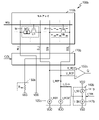
110 セルアレイ
120 電流源回路
130 レファレンス抵抗回路
140 オフセット電流回路
150 増幅回路
160 制御回路
200 コントローラ
CMD コマンド
ADDR アドレス
DATA データ
Claims (9)
- 読出コマンドに応答してメモリセルに保存された値を出力する抵抗性メモリ装置であって、
メモリセル及びレファレンスセルを含むセルアレイと、
前記レファレンスセルと電気的に連結されるように構成されたレファレンス抵抗回路と、
前記レファレンスセルを通過する読出電流にオフセット電流を付け加えるか、引き出すことで、前記レファレンス抵抗回路を通過するレファレンス電流を生成するように構成されたオフセット電流源回路と、
前記メモリセルの抵抗値の変動を補償するように、前記オフセット電流源回路を制御するように構成された制御回路と、を含む抵抗性メモリ装置。 - 前記制御回路は、前記抵抗性メモリ装置の温度に基づいて前記オフセット電流の大きさを調節するように、さらに構成されたことを特徴とする請求項1に記載の抵抗性メモリ装置。
- 前記オフセット電流源回路は、制御信号に従って前記オフセット電流の大きさを調節するように、さらに構成され、
前記制御回路は、
温度に比例する第1信号を生成するように構成された第1信号生成器と、
温度に反比例する第2信号を生成するように構成された第2信号生成器と、
前記第1信号及び前記第2信号の加重和として前記制御信号を生成する組合わせ回路と、を含み、
前記加重和の加重値は、前記メモリセルの抵抗値の温度変動特性によって決定されることを特徴とする請求項2に記載の抵抗性メモリ装置。 - 前記オフセット電流源回路は、制御信号に従って前記オフセット電流の大きさを調節するように、さらに構成され、
前記制御回路は、ルックアップテーブルを含み、前記ルックアップテーブルを参照することで、前記抵抗性メモリ装置の温度に従った温度信号から前記制御信号を生成するように、さらに構成されたことを特徴とする請求項2に記載の抵抗性メモリ装置。 - 前記制御回路によってアクセスされ、工程情報を保存するように構成された不揮発性メモリをさらに含み、
前記制御回路は、前記工程情報に基づいて前記オフセット電流の大きさを調節するように、さらに構成されたことを特徴とする請求項1に記載の抵抗性メモリ装置。 - 前記制御回路は、前記抵抗性メモリ装置の正の供給電圧の大きさに基づいて前記オフセット電流の大きさを調節するように、さらに構成されたことを特徴とする請求項1に記載の抵抗性メモリ装置。
- 読出コマンドに応答してメモリセルに保存された値を出力する抵抗性メモリ装置であって、
第1読出電流が通過するメモリセル及び第2読出電流が通過するレファレンスセルを含むセルアレイと、
前記第1読出電流及び前記第2読出電流を生成する電流源回路と、
前記第2読出電流にオフセット電流を付け加えるか、引き出すことで、レファレンス電流を生成するように構成されたオフセット電流源回路と、
前記レファレンスセルと電気的に連結され、前記レファレンス電流が通過するレファレンス抵抗回路と、
前記メモリセルの抵抗値の変動を補償するように、前記オフセット電流源回路を制御する制御回路と、を含む抵抗性メモリ装置。 - 前記第1読出電流及び前記第2読出電流は、近似的に等しいことを特徴とする請求項7に記載の抵抗性メモリ装置。
- 読出コマンドに応答してメモリセルに保存された値を出力する抵抗性メモリ装置であって、
第1読出電流が通過するメモリセル及び第2読出電流が通過するレファレンスセルを含むセルアレイと、
前記第2読出電流にオフセット電流を付け加えるか、引き出すことで、レファレンス電流を生成するように構成されたオフセット電流源回路と、
前記レファレンスセルと電気的に連結され、前記レファレンス電流が通過するレファレンス抵抗回路と、
前記メモリセルの抵抗値の変動を補償するように、前記オフセット電流源回路を制御するように構成された制御回路と、を含む抵抗性メモリ装置。
Applications Claiming Priority (4)
| Application Number | Priority Date | Filing Date | Title |
|---|---|---|---|
| KR10-2017-0118844 | 2017-09-15 | ||
| KR20170118844 | 2017-09-15 | ||
| KR1020180020007A KR102532204B1 (ko) | 2017-09-15 | 2018-02-20 | 레퍼런스 셀을 포함하는 저항성 메모리 장치 및 그것의 동작 방법 |
| KR10-2018-0020007 | 2018-02-20 |
Publications (2)
| Publication Number | Publication Date |
|---|---|
| JP2019053812A JP2019053812A (ja) | 2019-04-04 |
| JP7190844B2 true JP7190844B2 (ja) | 2022-12-16 |
Family
ID=65907787
Family Applications (1)
| Application Number | Title | Priority Date | Filing Date |
|---|---|---|---|
| JP2018155434A Active JP7190844B2 (ja) | 2017-09-15 | 2018-08-22 | レファレンスセルを含む抵抗性メモリ装置及びそれの動作方法 |
Country Status (3)
| Country | Link |
|---|---|
| JP (1) | JP7190844B2 (ja) |
| KR (1) | KR102532204B1 (ja) |
| TW (1) | TWI776951B (ja) |
Families Citing this family (7)
| Publication number | Priority date | Publication date | Assignee | Title |
|---|---|---|---|---|
| US10832783B1 (en) * | 2019-09-24 | 2020-11-10 | Macronix International Co., Ltd. | Data sensing device and data sensing method thereof |
| US11636322B2 (en) * | 2020-01-03 | 2023-04-25 | Silicon Storage Technology, Inc. | Precise data tuning method and apparatus for analog neural memory in an artificial neural network |
| US11574678B2 (en) * | 2020-09-17 | 2023-02-07 | Fujitsu Semiconductor Memory Solution Limited | Resistive random access memory, and method for manufacturing resistive random access memory |
| US11361821B2 (en) * | 2020-11-10 | 2022-06-14 | International Business Machines Corporation | Drift and noise corrected memristive device |
| KR102877891B1 (ko) * | 2021-04-07 | 2025-10-30 | 삼성전자주식회사 | 메모리 셀의 크기에 따른 최적의 읽기 전류를 생성하는 메모리 장치 |
| KR102863412B1 (ko) * | 2021-04-16 | 2025-09-24 | 삼성전자주식회사 | 메모리 셀의 크기 및 초기 쓰기 전압의 값에 기반하여 최적의 쓰기 전압을 생성하는 메모리 장치 |
| JP7788968B2 (ja) * | 2022-03-24 | 2025-12-19 | 株式会社東芝 | 基準電位生成回路および半導体記憶装置 |
Citations (4)
| Publication number | Priority date | Publication date | Assignee | Title |
|---|---|---|---|---|
| US20130265820A1 (en) | 2012-04-10 | 2013-10-10 | Taiwan Semiconductor Manufacturing Co., Ltd. | Adjusting reference resistances in determining mram resistance states |
| US20160343421A1 (en) | 2015-05-18 | 2016-11-24 | Suk-Soo Pyo | Memory device and memory system including the same |
| US20170062032A1 (en) | 2015-09-02 | 2017-03-02 | Bo-Young Seo | Semiconductor memory device including shorted variable resistor element of memory cell |
| JP2017134625A (ja) | 2016-01-28 | 2017-08-03 | ラピスセミコンダクタ株式会社 | 基準電流生成回路及びメモリ装置 |
Family Cites Families (11)
| Publication number | Priority date | Publication date | Assignee | Title |
|---|---|---|---|---|
| US7453719B2 (en) * | 2003-04-21 | 2008-11-18 | Nec Corporation | Magnetic random access memory with improved data reading method |
| KR100735677B1 (ko) * | 2005-12-28 | 2007-07-04 | 삼성전자주식회사 | 스탠바이 전류 저감 회로 및 이를 구비한 반도체 메모리장치 |
| US7471582B2 (en) * | 2006-07-28 | 2008-12-30 | Freescale Semiconductor, Inc. | Memory circuit using a reference for sensing |
| KR101083302B1 (ko) * | 2009-05-13 | 2011-11-15 | 주식회사 하이닉스반도체 | 반도체 메모리 장치 |
| US8274819B2 (en) * | 2010-02-04 | 2012-09-25 | Magic Technologies | Read disturb free SMT MRAM reference cell circuit |
| US8254195B2 (en) * | 2010-06-01 | 2012-08-28 | Qualcomm Incorporated | High-speed sensing for resistive memories |
| US8559243B2 (en) * | 2010-11-22 | 2013-10-15 | Infineon Technologies Ag | Self timed current integrating scheme employing level and slope detection |
| US9442838B2 (en) * | 2012-10-22 | 2016-09-13 | Rambus Inc. | Remapping memory cells based on future endurance measurements |
| CN106233392B (zh) * | 2014-03-07 | 2019-03-29 | 东芝存储器株式会社 | 存储器设备 |
| US9601165B1 (en) * | 2015-09-24 | 2017-03-21 | Intel IP Corporation | Sense amplifier |
| US9679643B1 (en) * | 2016-03-09 | 2017-06-13 | Taiwan Semiconductor Manufacturing Co., Ltd. | Resistive memory device having a trimmable resistance of at least on of a driver and a sinker is trimmed based on a row location |
-
2018
- 2018-02-20 KR KR1020180020007A patent/KR102532204B1/ko active Active
- 2018-08-22 JP JP2018155434A patent/JP7190844B2/ja active Active
- 2018-09-12 TW TW107131958A patent/TWI776951B/zh active
Patent Citations (4)
| Publication number | Priority date | Publication date | Assignee | Title |
|---|---|---|---|---|
| US20130265820A1 (en) | 2012-04-10 | 2013-10-10 | Taiwan Semiconductor Manufacturing Co., Ltd. | Adjusting reference resistances in determining mram resistance states |
| US20160343421A1 (en) | 2015-05-18 | 2016-11-24 | Suk-Soo Pyo | Memory device and memory system including the same |
| US20170062032A1 (en) | 2015-09-02 | 2017-03-02 | Bo-Young Seo | Semiconductor memory device including shorted variable resistor element of memory cell |
| JP2017134625A (ja) | 2016-01-28 | 2017-08-03 | ラピスセミコンダクタ株式会社 | 基準電流生成回路及びメモリ装置 |
Also Published As
| Publication number | Publication date |
|---|---|
| KR20190031108A (ko) | 2019-03-25 |
| JP2019053812A (ja) | 2019-04-04 |
| TW201916040A (zh) | 2019-04-16 |
| TWI776951B (zh) | 2022-09-11 |
| KR102532204B1 (ko) | 2023-05-16 |
Similar Documents
| Publication | Publication Date | Title |
|---|---|---|
| CN109509497B (zh) | 电阻式存储器装置 | |
| USRE50133E1 (en) | Resistive memory device including reference cell to compensate for a leakage current | |
| KR102532204B1 (ko) | 레퍼런스 셀을 포함하는 저항성 메모리 장치 및 그것의 동작 방법 | |
| US10964387B2 (en) | Resistive memory device including reference cell and operating method thereof | |
| CN110289028B (zh) | 用于读出放大器的控制信号发生器和包括其的存储器设备 | |
| US10762958B2 (en) | Resistive memory device including a reference cell and method of controlling a reference cell to identify values stored in memory cells | |
| CN110491431B (zh) | 校准参考电阻器的电阻式存储器装置 | |
| CN104681090B (zh) | 控制单元晶体管的接口状态提高感测界限的电阻存储装置 | |
| US9165646B2 (en) | Resistive memory device including compensation resistive device and method of compensating resistance distribution | |
| JP7288292B2 (ja) | レファレンスセルを含む抵抗性メモリ装置及びレファレンスセルの制御方法 | |
| KR102324769B1 (ko) | 반도체 메모리 장치의 에러 정정 회로, 반도체 메모리 장치 및 이를 포함하는 메모리 시스템 | |
| US20250014620A1 (en) | Memory device comprising memory cells storing calibration data and operating method thereof | |
| KR20190130445A (ko) | 레퍼런스 교정을 제공하는 저항성 메모리 장치 및 그것의 동작 방법 | |
| KR102414184B1 (ko) | 레퍼런스 셀을 포함하는 저항성 메모리 장치 및 그것의 동작 방법 | |
| KR20250008436A (ko) | 교정 데이터를 저장하는 메모리 셀들을 포함하는 메모리 장치 및 그것의 동작 방법 |
Legal Events
| Date | Code | Title | Description |
|---|---|---|---|
| A621 | Written request for application examination |
Free format text: JAPANESE INTERMEDIATE CODE: A621 Effective date: 20210629 |
|
| A977 | Report on retrieval |
Free format text: JAPANESE INTERMEDIATE CODE: A971007 Effective date: 20220615 |
|
| A131 | Notification of reasons for refusal |
Free format text: JAPANESE INTERMEDIATE CODE: A131 Effective date: 20220621 |
|
| A521 | Request for written amendment filed |
Free format text: JAPANESE INTERMEDIATE CODE: A523 Effective date: 20220902 |
|
| TRDD | Decision of grant or rejection written | ||
| A01 | Written decision to grant a patent or to grant a registration (utility model) |
Free format text: JAPANESE INTERMEDIATE CODE: A01 Effective date: 20221129 |
|
| A61 | First payment of annual fees (during grant procedure) |
Free format text: JAPANESE INTERMEDIATE CODE: A61 Effective date: 20221206 |
|
| R150 | Certificate of patent or registration of utility model |
Ref document number: 7190844 Country of ref document: JP Free format text: JAPANESE INTERMEDIATE CODE: R150 |
|
| R250 | Receipt of annual fees |
Free format text: JAPANESE INTERMEDIATE CODE: R250 |