JP7166375B2 - 物体の表面の光学的三次元トポグラフィ計測システム - Google Patents
物体の表面の光学的三次元トポグラフィ計測システム Download PDFInfo
- Publication number
- JP7166375B2 JP7166375B2 JP2021031926A JP2021031926A JP7166375B2 JP 7166375 B2 JP7166375 B2 JP 7166375B2 JP 2021031926 A JP2021031926 A JP 2021031926A JP 2021031926 A JP2021031926 A JP 2021031926A JP 7166375 B2 JP7166375 B2 JP 7166375B2
- Authority
- JP
- Japan
- Prior art keywords
- objective
- illumination
- grating
- pattern
- patterned
- Prior art date
- Legal status (The legal status is an assumption and is not a legal conclusion. Google has not performed a legal analysis and makes no representation as to the accuracy of the status listed.)
- Active
Links
Images

Classifications
-
- G—PHYSICS
- G01—MEASURING; TESTING
- G01B—MEASURING LENGTH, THICKNESS OR SIMILAR LINEAR DIMENSIONS; MEASURING ANGLES; MEASURING AREAS; MEASURING IRREGULARITIES OF SURFACES OR CONTOURS
- G01B11/00—Measuring arrangements characterised by the use of optical techniques
- G01B11/24—Measuring arrangements characterised by the use of optical techniques for measuring contours or curvatures
- G01B11/25—Measuring arrangements characterised by the use of optical techniques for measuring contours or curvatures by projecting a pattern, e.g. one or more lines, moiré fringes on the object
- G01B11/2518—Projection by scanning of the object
-
- G—PHYSICS
- G01—MEASURING; TESTING
- G01B—MEASURING LENGTH, THICKNESS OR SIMILAR LINEAR DIMENSIONS; MEASURING ANGLES; MEASURING AREAS; MEASURING IRREGULARITIES OF SURFACES OR CONTOURS
- G01B11/00—Measuring arrangements characterised by the use of optical techniques
- G01B11/02—Measuring arrangements characterised by the use of optical techniques for measuring length, width or thickness
- G01B11/06—Measuring arrangements characterised by the use of optical techniques for measuring length, width or thickness for measuring thickness ; e.g. of sheet material
- G01B11/0608—Height gauges
-
- G—PHYSICS
- G01—MEASURING; TESTING
- G01B—MEASURING LENGTH, THICKNESS OR SIMILAR LINEAR DIMENSIONS; MEASURING ANGLES; MEASURING AREAS; MEASURING IRREGULARITIES OF SURFACES OR CONTOURS
- G01B11/00—Measuring arrangements characterised by the use of optical techniques
- G01B11/24—Measuring arrangements characterised by the use of optical techniques for measuring contours or curvatures
- G01B11/25—Measuring arrangements characterised by the use of optical techniques for measuring contours or curvatures by projecting a pattern, e.g. one or more lines, moiré fringes on the object
- G01B11/2513—Measuring arrangements characterised by the use of optical techniques for measuring contours or curvatures by projecting a pattern, e.g. one or more lines, moiré fringes on the object with several lines being projected in more than one direction, e.g. grids, patterns
-
- G—PHYSICS
- G01—MEASURING; TESTING
- G01B—MEASURING LENGTH, THICKNESS OR SIMILAR LINEAR DIMENSIONS; MEASURING ANGLES; MEASURING AREAS; MEASURING IRREGULARITIES OF SURFACES OR CONTOURS
- G01B11/00—Measuring arrangements characterised by the use of optical techniques
- G01B11/24—Measuring arrangements characterised by the use of optical techniques for measuring contours or curvatures
- G01B11/25—Measuring arrangements characterised by the use of optical techniques for measuring contours or curvatures by projecting a pattern, e.g. one or more lines, moiré fringes on the object
- G01B11/2518—Projection by scanning of the object
- G01B11/2522—Projection by scanning of the object the position of the object changing and being recorded
-
- G—PHYSICS
- G01—MEASURING; TESTING
- G01N—INVESTIGATING OR ANALYSING MATERIALS BY DETERMINING THEIR CHEMICAL OR PHYSICAL PROPERTIES
- G01N21/00—Investigating or analysing materials by the use of optical means, i.e. using sub-millimetre waves, infrared, visible or ultraviolet light
- G01N21/17—Systems in which incident light is modified in accordance with the properties of the material investigated
- G01N21/25—Colour; Spectral properties, i.e. comparison of effect of material on the light at two or more different wavelengths or wavelength bands
- G01N21/31—Investigating relative effect of material at wavelengths characteristic of specific elements or molecules, e.g. atomic absorption spectrometry
- G01N21/39—Investigating relative effect of material at wavelengths characteristic of specific elements or molecules, e.g. atomic absorption spectrometry using tunable lasers
-
- G—PHYSICS
- G01—MEASURING; TESTING
- G01N—INVESTIGATING OR ANALYSING MATERIALS BY DETERMINING THEIR CHEMICAL OR PHYSICAL PROPERTIES
- G01N21/00—Investigating or analysing materials by the use of optical means, i.e. using sub-millimetre waves, infrared, visible or ultraviolet light
- G01N21/84—Systems specially adapted for particular applications
- G01N21/88—Investigating the presence of flaws or contamination
- G01N21/95—Investigating the presence of flaws or contamination characterised by the material or shape of the object to be examined
- G01N21/956—Inspecting patterns on the surface of objects
-
- G—PHYSICS
- G02—OPTICS
- G02B—OPTICAL ELEMENTS, SYSTEMS OR APPARATUS
- G02B30/00—Optical systems or apparatus for producing three-dimensional [3D] effects, e.g. stereoscopic images
- G02B30/50—Optical systems or apparatus for producing three-dimensional [3D] effects, e.g. stereoscopic images the image being built up from image elements distributed over a three-dimensional [3D] volume, e.g. voxels
-
- G—PHYSICS
- G01—MEASURING; TESTING
- G01B—MEASURING LENGTH, THICKNESS OR SIMILAR LINEAR DIMENSIONS; MEASURING ANGLES; MEASURING AREAS; MEASURING IRREGULARITIES OF SURFACES OR CONTOURS
- G01B2210/00—Aspects not specifically covered by any group under G01B, e.g. of wheel alignment, caliper-like sensors
- G01B2210/56—Measuring geometric parameters of semiconductor structures, e.g. profile, critical dimensions or trench depth
-
- G—PHYSICS
- G01—MEASURING; TESTING
- G01N—INVESTIGATING OR ANALYSING MATERIALS BY DETERMINING THEIR CHEMICAL OR PHYSICAL PROPERTIES
- G01N21/00—Investigating or analysing materials by the use of optical means, i.e. using sub-millimetre waves, infrared, visible or ultraviolet light
- G01N21/17—Systems in which incident light is modified in accordance with the properties of the material investigated
- G01N21/25—Colour; Spectral properties, i.e. comparison of effect of material on the light at two or more different wavelengths or wavelength bands
- G01N21/31—Investigating relative effect of material at wavelengths characteristic of specific elements or molecules, e.g. atomic absorption spectrometry
- G01N21/39—Investigating relative effect of material at wavelengths characteristic of specific elements or molecules, e.g. atomic absorption spectrometry using tunable lasers
- G01N2021/395—Investigating relative effect of material at wavelengths characteristic of specific elements or molecules, e.g. atomic absorption spectrometry using tunable lasers using a topographic target
Landscapes
- Physics & Mathematics (AREA)
- General Physics & Mathematics (AREA)
- Computer Vision & Pattern Recognition (AREA)
- Engineering & Computer Science (AREA)
- Life Sciences & Earth Sciences (AREA)
- Chemical & Material Sciences (AREA)
- Analytical Chemistry (AREA)
- Biochemistry (AREA)
- General Health & Medical Sciences (AREA)
- Immunology (AREA)
- Pathology (AREA)
- Spectroscopy & Molecular Physics (AREA)
- Health & Medical Sciences (AREA)
- Optics & Photonics (AREA)
- Length Measuring Devices By Optical Means (AREA)
- Investigating Or Analysing Materials By Optical Means (AREA)
Description
本願は、この参照を以てその全容が本願に繰り入れられるところの2016年2月1日付米国暫定特許出願第62/289889号に基づく優先権を主張する出願である。
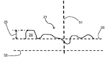
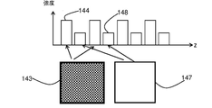
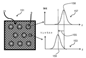
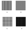
諸実施形態では、そのパターンマスクが、これに限られるものではないが市松模様又はピンホールアレイを有するものとされる。本件技術分野で既知な他のパターン化照明生成向けパターンも遜色なく用いうる。
1.格子ピッチ(Λ)を小さくすること
2.フリンジコントラスト(C0)を高めること
3.光学系により制限される照明数値開口(NAi)を高めること
4.センサにより制限される画像ダイナミックレンジの逆数を大きくすること
5.データレート及びスループットにより制限される計測回数を増やすこと
で、計測再現性を改善することができる。


Claims (12)
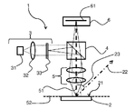
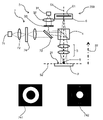
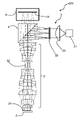
- 物体の表面の光学的三次元トポグラフィ計測システムであって、
パターン化照明源と、
均一照明源と、
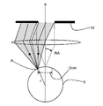
前記パターン化照明及び前記均一照明双方を前記物体の表面に差し向けるよう配置された対物系と、
前記対物系を介し前記物体の表面の画像を複数枚記録するよう配置及び構成された検出器と、
前記検出器に接続され、前記複数枚の画像のうち、前記パターン化照明下で記録された画像の光強度差、及び前記均一照明下で記録された画像の光強度差に基づき前記物体の表面の位置の高さ情報を決定するように構成されたコンピュータと、
を備え、前記光強度は、前記物体の光軸に沿った1つの方向に沿って変化する、
システム。 - 請求項1に記載のシステムにおいて、
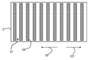
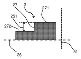
前記パターン化照明源が光源及びパターンマスクを有するシステム。 - 請求項2に記載のシステムにおいて、
前記パターンマスクが市松模様又はピンホールアレイを有するシステム。 - 請求項2に記載のシステムにおいて、
前記パターンマスクが格子であるシステム。 - 請求項4に記載のシステムにおいて、
前記格子が振幅格子又は位相格子であるシステム。 - 請求項4に記載のシステムにおいて、
前記格子がライン格子又は正弦格子又はクロスライン格子であるシステム。 - 請求項4に記載のシステムにおいて、
前記格子がブレーズド格子であるシステム。 - 請求項1に記載のシステムにおいて、
前記対物系・前記検出器間の撮像路と、少なくとも前記パターン化照明源・前記対物系間の照明路と前記均一照明源・前記対物系間の照明路のいずれか1つとが、ビームスプリッタを通過する形態で、前記ビームスプリッタが配置されているシステム。 - 請求項8に記載のシステムにおいて、
前記パターン化照明源・前記対物系間の照明路と前記均一照明源・前記対物系間の照明路の双方が、前記ビームスプリッタを通過するシステム。 - 請求項8に記載のシステムにおいて、前記対物系は前記ビームスプリッタにより生じた回折を補正するように配置されるシステム。
- 請求項2に記載のシステムにおいて、
前記パターンマスク及び前記検出器が共役平面内に存するシステム。 - 請求項1に記載のシステムにおいて、
前記物体と前記対物系の相対運動の方向が前記対物系の光軸に対し平行であるシステム。
Applications Claiming Priority (2)
| Application Number | Priority Date | Filing Date | Title |
|---|---|---|---|
| US201662289889P | 2016-02-01 | 2016-02-01 | |
| US62/289,889 | 2016-02-01 |
Related Parent Applications (1)
| Application Number | Title | Priority Date | Filing Date |
|---|---|---|---|
| JP2018559667A Division JP6846441B2 (ja) | 2016-02-01 | 2016-11-04 | 物体の表面の光学的三次元トポグラフィ計測システム |
Publications (2)
| Publication Number | Publication Date |
|---|---|
| JP2021081446A JP2021081446A (ja) | 2021-05-27 |
| JP7166375B2 true JP7166375B2 (ja) | 2022-11-07 |
Family
ID=59500792
Family Applications (2)
| Application Number | Title | Priority Date | Filing Date |
|---|---|---|---|
| JP2018559667A Active JP6846441B2 (ja) | 2016-02-01 | 2016-11-04 | 物体の表面の光学的三次元トポグラフィ計測システム |
| JP2021031926A Active JP7166375B2 (ja) | 2016-02-01 | 2021-03-01 | 物体の表面の光学的三次元トポグラフィ計測システム |
Family Applications Before (1)
| Application Number | Title | Priority Date | Filing Date |
|---|---|---|---|
| JP2018559667A Active JP6846441B2 (ja) | 2016-02-01 | 2016-11-04 | 物体の表面の光学的三次元トポグラフィ計測システム |
Country Status (12)
| Country | Link |
|---|---|
| US (2) | US10634487B2 (ja) |
| EP (2) | EP3411695B1 (ja) |
| JP (2) | JP6846441B2 (ja) |
| KR (1) | KR102668017B1 (ja) |
| CN (2) | CN108603848B (ja) |
| ES (1) | ES2908695T3 (ja) |
| MY (2) | MY196634A (ja) |
| PH (1) | PH12018501598A1 (ja) |
| PT (1) | PT3411695T (ja) |
| SG (2) | SG10201912769PA (ja) |
| TW (2) | TWI723129B (ja) |
| WO (1) | WO2017136011A2 (ja) |
Families Citing this family (15)
| Publication number | Priority date | Publication date | Assignee | Title |
|---|---|---|---|---|
| JP6189984B2 (ja) * | 2016-02-12 | 2017-08-30 | Ckd株式会社 | 三次元計測装置 |
| NL2020619B1 (en) * | 2018-01-16 | 2019-07-25 | Illumina Inc | Dual optical grating slide structured illumination imaging |
| KR102066129B1 (ko) * | 2018-09-21 | 2020-01-14 | 한양대학교 산학협력단 | 도트 어레이를 이용하는 3차원 정보 생성 장치 및 방법 |
| US10704094B1 (en) | 2018-11-14 | 2020-07-07 | Element Biosciences, Inc. | Multipart reagents having increased avidity for polymerase binding |
| KR102008890B1 (ko) | 2019-01-25 | 2019-08-08 | 단국대학교 산학협력단 | 3차원 프로파일 측정 방법 |
| KR102260563B1 (ko) * | 2019-07-02 | 2021-06-07 | 한국과학기술연구원 | 체커보드 패턴 기반 구조 조명 현미경 시스템 |
| US10921721B1 (en) * | 2019-09-13 | 2021-02-16 | Applied Materials, Inc. | Measurement system and grating pattern array |
| US11060138B1 (en) | 2020-01-17 | 2021-07-13 | Element Biosciences, Inc. | Nucleic acid sequencing systems |
| DE102020201536A1 (de) * | 2020-02-07 | 2021-08-12 | Fraunhofer-Gesellschaft zur Förderung der angewandten Forschung eingetragener Verein | Verfahren und Vorrichtung zum berührungslosen Vermessen einer Objektoberfläche |
| CN111721231B (zh) * | 2020-06-03 | 2021-11-19 | 华东师范大学 | 一种基于光频梳的植物生态监测系统 |
| US20230280282A1 (en) * | 2020-07-13 | 2023-09-07 | Camtek Ltd. | Continuous bump measurement height metrology |
| WO2022013703A1 (en) * | 2020-07-13 | 2022-01-20 | Camtek Ltd. | Continuous bump measurement height metrology |
| AU2022316142A1 (en) | 2021-07-21 | 2024-02-22 | Element Biosciences, Inc. | Optical systems for nucleic acid sequencing and methods thereof |
| US12169920B2 (en) | 2022-01-05 | 2024-12-17 | Honeywell Federal Manufacturing & Technologies, Llc | Telecentric detection of lattice breakdown |
| CN121048525A (zh) * | 2025-08-21 | 2025-12-02 | 苏州明鉴传感科技有限公司 | 基于掩膜版的明场三维重建装置和方法 |
Citations (2)
| Publication number | Priority date | Publication date | Assignee | Title |
|---|---|---|---|---|
| JP2011523057A (ja) | 2008-06-05 | 2011-08-04 | トラスティーズ オブ ボストン ユニバーシティ | 構造化された照射および均一な照射の両方を用いて光学的に切片化された画像を生成するためのシステムおよび方法 |
| US20140376064A1 (en) | 2013-06-21 | 2014-12-25 | 3Shape A/S | Scanning apparatus with patterned probe light |
Family Cites Families (39)
| Publication number | Priority date | Publication date | Assignee | Title |
|---|---|---|---|---|
| US6249335B1 (en) * | 1992-01-17 | 2001-06-19 | Nikon Corporation | Photo-mask and method of exposing and projection-exposing apparatus |
| US5248876A (en) * | 1992-04-21 | 1993-09-28 | International Business Machines Corporation | Tandem linear scanning confocal imaging system with focal volumes at different heights |
| US5471303A (en) * | 1994-04-29 | 1995-11-28 | Wyko Corporation | Combination of white-light scanning and phase-shifting interferometry for surface profile measurements |
| JPH11211439A (ja) * | 1998-01-22 | 1999-08-06 | Takaoka Electric Mfg Co Ltd | 表面形状計測装置 |
| AU3991799A (en) * | 1998-05-14 | 1999-11-29 | Metacreations Corporation | Structured-light, triangulation-based three-dimensional digitizer |
| GB9901365D0 (en) * | 1999-01-22 | 1999-03-10 | Isis Innovations Ltd | Confocal microscopy apparatus and method |
| US6268923B1 (en) | 1999-10-07 | 2001-07-31 | Integral Vision, Inc. | Optical method and system for measuring three-dimensional surface topography of an object having a surface contour |
| FI20001568L (fi) * | 2000-06-30 | 2001-12-31 | Thermo Radiometrie Oy | Pinnan muotojen määrittäminen |
| US6724489B2 (en) * | 2000-09-22 | 2004-04-20 | Daniel Freifeld | Three dimensional scanning camera |
| US6870609B2 (en) | 2001-02-09 | 2005-03-22 | August Technology Corp. | Confocal 3D inspection system and process |
| US20020145734A1 (en) | 2001-02-09 | 2002-10-10 | Cory Watkins | Confocal 3D inspection system and process |
| US6893800B2 (en) | 2002-09-24 | 2005-05-17 | Agere Systems, Inc. | Substrate topography compensation at mask design: 3D OPC topography anchored |
| US7126699B1 (en) | 2002-10-18 | 2006-10-24 | Kla-Tencor Technologies Corp. | Systems and methods for multi-dimensional metrology and/or inspection of a specimen |
| US7286246B2 (en) * | 2003-03-31 | 2007-10-23 | Mitutoyo Corporation | Method and apparatus for non-contact three-dimensional surface measurement |
| DE10321888A1 (de) * | 2003-05-07 | 2004-12-02 | Universität Stuttgart | Messverfahren und Sensor, insbesondere zur optischen Abtastung bewegter Objekte |
| US7680013B2 (en) * | 2005-11-29 | 2010-03-16 | Canon Kabushiki Kaisha | Optical information recording and reproducing apparatus |
| JP2008003520A (ja) * | 2006-06-26 | 2008-01-10 | Toshiba Corp | フォトマスク及び半導体装置の製造方法 |
| JP4991872B2 (ja) * | 2006-11-01 | 2012-08-01 | インフェーズ テクノロジィズ インコーポレイテッド | モノキュラーホログラフィックデータ記憶システムの構成 |
| CN102802529B (zh) * | 2009-06-16 | 2015-09-16 | 皇家飞利浦电子股份有限公司 | 用于微分相衬成像的校正方法 |
| CA2763826C (en) * | 2009-06-17 | 2020-04-07 | 3Shape A/S | Focus scanning apparatus |
| US8754936B2 (en) * | 2009-07-03 | 2014-06-17 | Koh Young Technology Inc. | Three dimensional shape measurement apparatus |
| KR101121982B1 (ko) * | 2009-07-03 | 2012-03-09 | 주식회사 고영테크놀러지 | 3차원 형상 측정장치 |
| EP2327956B1 (en) * | 2009-11-20 | 2014-01-22 | Mitutoyo Corporation | Method and apparatus for determining the height of a number of spatial positions on a sample |
| JP5942847B2 (ja) * | 2010-05-07 | 2016-06-29 | 株式会社ニコン | 高さ測定方法及び高さ測定装置 |
| EP2437027A3 (de) * | 2010-10-03 | 2012-05-30 | Confovis GmbH | Vorrichtung und Verfahren zur dreidimensionalen optischen Abtastung einer Probe |
| US8649024B2 (en) * | 2010-12-03 | 2014-02-11 | Zygo Corporation | Non-contact surface characterization using modulated illumination |
| US10048480B2 (en) * | 2011-01-07 | 2018-08-14 | Zeta Instruments, Inc. | 3D microscope including insertable components to provide multiple imaging and measurement capabilities |
| US8610902B2 (en) | 2011-06-02 | 2013-12-17 | Asm Technology Singapore Pte Ltd | Apparatus and method for inspecting an object with increased depth of field |
| DE102012017922B4 (de) * | 2012-09-11 | 2024-03-14 | Carl Zeiss Microscopy Gmbh | Optikanordnung und Lichtmikroskop |
| US9255791B2 (en) * | 2012-09-28 | 2016-02-09 | The Board Of Trustees Of The University Of Illinois | Optically monitoring and controlling nanoscale topography |
| CN104180773B (zh) * | 2013-05-20 | 2017-07-21 | 沈阳同联集团高新技术有限公司 | 一种三维形貌测量装置 |
| CN103292740B (zh) * | 2013-05-24 | 2016-04-13 | 贵阳嘉瑜光电科技咨询中心 | 一种三维扫描仪测量方法及其装置 |
| CN103424795B (zh) * | 2013-09-03 | 2015-10-28 | 苏州大学 | 一种反射式分光光栅及干涉光刻系统 |
| TWI489101B (zh) * | 2013-12-02 | 2015-06-21 | Ind Tech Res Inst | 結合三維及二維形貌之量測方法及裝置 |
| WO2015105980A1 (en) * | 2014-01-09 | 2015-07-16 | Zygo Corporation | Measuring topography of aspheric and other non-flat surfaces |
| JP6656177B2 (ja) * | 2014-06-13 | 2020-03-04 | スリーエム イノベイティブ プロパティズ カンパニー | スパークルを低減するための光学積層体 |
| JP6355262B2 (ja) * | 2015-03-10 | 2018-07-11 | 富士フイルム株式会社 | 計測システム、計測方法及び計測プログラム |
| JP6702669B2 (ja) * | 2015-07-29 | 2020-06-03 | キヤノン株式会社 | 撮像装置及びその制御方法 |
| JP6682310B2 (ja) * | 2016-03-18 | 2020-04-15 | キヤノン株式会社 | 焦点検出装置および方法、および撮像装置 |
-
2016
- 2016-11-04 ES ES16889639T patent/ES2908695T3/es active Active
- 2016-11-04 SG SG10201912769PA patent/SG10201912769PA/en unknown
- 2016-11-04 KR KR1020187025110A patent/KR102668017B1/ko active Active
- 2016-11-04 EP EP16889639.7A patent/EP3411695B1/en active Active
- 2016-11-04 MY MYPI2018001022A patent/MY196634A/en unknown
- 2016-11-04 US US15/329,778 patent/US10634487B2/en active Active
- 2016-11-04 CN CN201680080685.2A patent/CN108603848B/zh active Active
- 2016-11-04 PT PT168896397T patent/PT3411695T/pt unknown
- 2016-11-04 SG SG11201805467TA patent/SG11201805467TA/en unknown
- 2016-11-04 WO PCT/US2016/060599 patent/WO2017136011A2/en not_active Ceased
- 2016-11-04 JP JP2018559667A patent/JP6846441B2/ja active Active
- 2016-11-04 EP EP21216084.0A patent/EP3998477B1/en active Active
- 2016-11-04 CN CN202110901243.2A patent/CN113607088B/zh active Active
- 2016-11-04 MY MYPI2022003523A patent/MY208359A/en unknown
-
2017
- 2017-02-02 TW TW106103528A patent/TWI723129B/zh active
- 2017-02-02 TW TW110107224A patent/TWI775331B/zh active
-
2018
- 2018-07-26 PH PH12018501598A patent/PH12018501598A1/en unknown
-
2020
- 2020-03-02 US US16/806,076 patent/US11287248B2/en active Active
-
2021
- 2021-03-01 JP JP2021031926A patent/JP7166375B2/ja active Active
Patent Citations (2)
| Publication number | Priority date | Publication date | Assignee | Title |
|---|---|---|---|---|
| JP2011523057A (ja) | 2008-06-05 | 2011-08-04 | トラスティーズ オブ ボストン ユニバーシティ | 構造化された照射および均一な照射の両方を用いて光学的に切片化された画像を生成するためのシステムおよび方法 |
| US20140376064A1 (en) | 2013-06-21 | 2014-12-25 | 3Shape A/S | Scanning apparatus with patterned probe light |
Also Published As
| Publication number | Publication date |
|---|---|
| KR102668017B1 (ko) | 2024-05-21 |
| KR20180101612A (ko) | 2018-09-12 |
| PT3411695T (pt) | 2022-03-03 |
| JP6846441B2 (ja) | 2021-03-24 |
| TWI723129B (zh) | 2021-04-01 |
| CN108603848A (zh) | 2018-09-28 |
| PH12018501598A1 (en) | 2019-04-08 |
| TWI775331B (zh) | 2022-08-21 |
| EP3411695A2 (en) | 2018-12-12 |
| JP2021081446A (ja) | 2021-05-27 |
| MY208359A (en) | 2025-05-01 |
| US20180209784A1 (en) | 2018-07-26 |
| CN113607088A (zh) | 2021-11-05 |
| TW202127008A (zh) | 2021-07-16 |
| SG11201805467TA (en) | 2018-08-30 |
| WO2017136011A3 (en) | 2018-02-22 |
| SG10201912769PA (en) | 2020-02-27 |
| CN108603848B (zh) | 2021-08-10 |
| EP3411695B1 (en) | 2022-01-26 |
| US11287248B2 (en) | 2022-03-29 |
| ES2908695T3 (es) | 2022-05-03 |
| EP3411695A4 (en) | 2019-10-02 |
| US10634487B2 (en) | 2020-04-28 |
| WO2017136011A2 (en) | 2017-08-10 |
| US20200217651A1 (en) | 2020-07-09 |
| MY196634A (en) | 2023-04-25 |
| JP2019503499A (ja) | 2019-02-07 |
| EP3998477A1 (en) | 2022-05-18 |
| CN113607088B (zh) | 2024-12-03 |
| EP3998477B1 (en) | 2025-01-08 |
| TW201732263A (zh) | 2017-09-16 |
Similar Documents
| Publication | Publication Date | Title |
|---|---|---|
| JP7166375B2 (ja) | 物体の表面の光学的三次元トポグラフィ計測システム | |
| TWI717019B (zh) | 經組態以產生包含複數個照明光束之量測照明之度量衡裝置及微影設備 | |
| KR100547437B1 (ko) | 리소그래피장치, 디바이스제조방법 및 이에 따라 제조된디바이스 | |
| TWI736089B (zh) | 位置度量衡裝置及相關聯光學元件 | |
| JP3401783B2 (ja) | 表面形状計測装置 | |
| TW201807389A (zh) | 決定波前像差的測量系統 | |
| JP2022043701A (ja) | 三次元計測装置 | |
| TW202144739A (zh) | 測量裝置、曝光裝置以及測量方法 | |
| CN113227906B (zh) | 位置量测设备和关联的光学元件 |
Legal Events
| Date | Code | Title | Description |
|---|---|---|---|
| A621 | Written request for application examination |
Free format text: JAPANESE INTERMEDIATE CODE: A621 Effective date: 20210301 |
|
| A131 | Notification of reasons for refusal |
Free format text: JAPANESE INTERMEDIATE CODE: A131 Effective date: 20220426 |
|
| A521 | Request for written amendment filed |
Free format text: JAPANESE INTERMEDIATE CODE: A523 Effective date: 20220725 |
|
| TRDD | Decision of grant or rejection written | ||
| A01 | Written decision to grant a patent or to grant a registration (utility model) |
Free format text: JAPANESE INTERMEDIATE CODE: A01 Effective date: 20221018 |
|
| A61 | First payment of annual fees (during grant procedure) |
Free format text: JAPANESE INTERMEDIATE CODE: A61 Effective date: 20221025 |
|
| R150 | Certificate of patent or registration of utility model |
Ref document number: 7166375 Country of ref document: JP Free format text: JAPANESE INTERMEDIATE CODE: R150 |
|
| R250 | Receipt of annual fees |
Free format text: JAPANESE INTERMEDIATE CODE: R250 |