JP7166375B2 - Optical three-dimensional topography measurement system for the surface of an object - Google Patents
Optical three-dimensional topography measurement system for the surface of an object Download PDFInfo
- Publication number
- JP7166375B2 JP7166375B2 JP2021031926A JP2021031926A JP7166375B2 JP 7166375 B2 JP7166375 B2 JP 7166375B2 JP 2021031926 A JP2021031926 A JP 2021031926A JP 2021031926 A JP2021031926 A JP 2021031926A JP 7166375 B2 JP7166375 B2 JP 7166375B2
- Authority
- JP
- Japan
- Prior art keywords
- objective
- illumination
- grating
- pattern
- patterned
- Prior art date
- Legal status (The legal status is an assumption and is not a legal conclusion. Google has not performed a legal analysis and makes no representation as to the accuracy of the status listed.)
- Active
Links
Images

Classifications
-
- G—PHYSICS
- G01—MEASURING; TESTING
- G01B—MEASURING LENGTH, THICKNESS OR SIMILAR LINEAR DIMENSIONS; MEASURING ANGLES; MEASURING AREAS; MEASURING IRREGULARITIES OF SURFACES OR CONTOURS
- G01B11/00—Measuring arrangements characterised by the use of optical techniques
- G01B11/24—Measuring arrangements characterised by the use of optical techniques for measuring contours or curvatures
- G01B11/25—Measuring arrangements characterised by the use of optical techniques for measuring contours or curvatures by projecting a pattern, e.g. one or more lines, moiré fringes on the object
- G01B11/2518—Projection by scanning of the object
-
- G—PHYSICS
- G01—MEASURING; TESTING
- G01B—MEASURING LENGTH, THICKNESS OR SIMILAR LINEAR DIMENSIONS; MEASURING ANGLES; MEASURING AREAS; MEASURING IRREGULARITIES OF SURFACES OR CONTOURS
- G01B11/00—Measuring arrangements characterised by the use of optical techniques
- G01B11/02—Measuring arrangements characterised by the use of optical techniques for measuring length, width or thickness
- G01B11/06—Measuring arrangements characterised by the use of optical techniques for measuring length, width or thickness for measuring thickness ; e.g. of sheet material
- G01B11/0608—Height gauges
-
- G—PHYSICS
- G01—MEASURING; TESTING
- G01B—MEASURING LENGTH, THICKNESS OR SIMILAR LINEAR DIMENSIONS; MEASURING ANGLES; MEASURING AREAS; MEASURING IRREGULARITIES OF SURFACES OR CONTOURS
- G01B11/00—Measuring arrangements characterised by the use of optical techniques
- G01B11/24—Measuring arrangements characterised by the use of optical techniques for measuring contours or curvatures
- G01B11/25—Measuring arrangements characterised by the use of optical techniques for measuring contours or curvatures by projecting a pattern, e.g. one or more lines, moiré fringes on the object
- G01B11/2513—Measuring arrangements characterised by the use of optical techniques for measuring contours or curvatures by projecting a pattern, e.g. one or more lines, moiré fringes on the object with several lines being projected in more than one direction, e.g. grids, patterns
-
- G—PHYSICS
- G01—MEASURING; TESTING
- G01B—MEASURING LENGTH, THICKNESS OR SIMILAR LINEAR DIMENSIONS; MEASURING ANGLES; MEASURING AREAS; MEASURING IRREGULARITIES OF SURFACES OR CONTOURS
- G01B11/00—Measuring arrangements characterised by the use of optical techniques
- G01B11/24—Measuring arrangements characterised by the use of optical techniques for measuring contours or curvatures
- G01B11/25—Measuring arrangements characterised by the use of optical techniques for measuring contours or curvatures by projecting a pattern, e.g. one or more lines, moiré fringes on the object
- G01B11/2518—Projection by scanning of the object
- G01B11/2522—Projection by scanning of the object the position of the object changing and being recorded
-
- G—PHYSICS
- G01—MEASURING; TESTING
- G01N—INVESTIGATING OR ANALYSING MATERIALS BY DETERMINING THEIR CHEMICAL OR PHYSICAL PROPERTIES
- G01N21/00—Investigating or analysing materials by the use of optical means, i.e. using sub-millimetre waves, infrared, visible or ultraviolet light
- G01N21/17—Systems in which incident light is modified in accordance with the properties of the material investigated
- G01N21/25—Colour; Spectral properties, i.e. comparison of effect of material on the light at two or more different wavelengths or wavelength bands
- G01N21/31—Investigating relative effect of material at wavelengths characteristic of specific elements or molecules, e.g. atomic absorption spectrometry
- G01N21/39—Investigating relative effect of material at wavelengths characteristic of specific elements or molecules, e.g. atomic absorption spectrometry using tunable lasers
-
- G—PHYSICS
- G01—MEASURING; TESTING
- G01N—INVESTIGATING OR ANALYSING MATERIALS BY DETERMINING THEIR CHEMICAL OR PHYSICAL PROPERTIES
- G01N21/00—Investigating or analysing materials by the use of optical means, i.e. using sub-millimetre waves, infrared, visible or ultraviolet light
- G01N21/84—Systems specially adapted for particular applications
- G01N21/88—Investigating the presence of flaws or contamination
- G01N21/95—Investigating the presence of flaws or contamination characterised by the material or shape of the object to be examined
- G01N21/956—Inspecting patterns on the surface of objects
-
- G—PHYSICS
- G02—OPTICS
- G02B—OPTICAL ELEMENTS, SYSTEMS OR APPARATUS
- G02B30/00—Optical systems or apparatus for producing three-dimensional [3D] effects, e.g. stereoscopic images
- G02B30/50—Optical systems or apparatus for producing three-dimensional [3D] effects, e.g. stereoscopic images the image being built up from image elements distributed over a three-dimensional [3D] volume, e.g. voxels
-
- G—PHYSICS
- G01—MEASURING; TESTING
- G01B—MEASURING LENGTH, THICKNESS OR SIMILAR LINEAR DIMENSIONS; MEASURING ANGLES; MEASURING AREAS; MEASURING IRREGULARITIES OF SURFACES OR CONTOURS
- G01B2210/00—Aspects not specifically covered by any group under G01B, e.g. of wheel alignment, caliper-like sensors
- G01B2210/56—Measuring geometric parameters of semiconductor structures, e.g. profile, critical dimensions or trench depth
-
- G—PHYSICS
- G01—MEASURING; TESTING
- G01N—INVESTIGATING OR ANALYSING MATERIALS BY DETERMINING THEIR CHEMICAL OR PHYSICAL PROPERTIES
- G01N21/00—Investigating or analysing materials by the use of optical means, i.e. using sub-millimetre waves, infrared, visible or ultraviolet light
- G01N21/17—Systems in which incident light is modified in accordance with the properties of the material investigated
- G01N21/25—Colour; Spectral properties, i.e. comparison of effect of material on the light at two or more different wavelengths or wavelength bands
- G01N21/31—Investigating relative effect of material at wavelengths characteristic of specific elements or molecules, e.g. atomic absorption spectrometry
- G01N21/39—Investigating relative effect of material at wavelengths characteristic of specific elements or molecules, e.g. atomic absorption spectrometry using tunable lasers
- G01N2021/395—Investigating relative effect of material at wavelengths characteristic of specific elements or molecules, e.g. atomic absorption spectrometry using tunable lasers using a topographic target
Landscapes
- Physics & Mathematics (AREA)
- General Physics & Mathematics (AREA)
- Computer Vision & Pattern Recognition (AREA)
- Engineering & Computer Science (AREA)
- Life Sciences & Earth Sciences (AREA)
- Chemical & Material Sciences (AREA)
- Analytical Chemistry (AREA)
- Biochemistry (AREA)
- General Health & Medical Sciences (AREA)
- Immunology (AREA)
- Pathology (AREA)
- Spectroscopy & Molecular Physics (AREA)
- Health & Medical Sciences (AREA)
- Optics & Photonics (AREA)
- Length Measuring Devices By Optical Means (AREA)
- Investigating Or Analysing Materials By Optical Means (AREA)
Description
本発明は物体の表面の三次元(3D)トポグラフィ計測方法及びシステム、特に対物系を介しその物体の表面上にパターン化照明を投射し、物体・対物系間相対運動中に記録されたその表面の画像からその表面についての高さ情報を取得するものに関する。 The present invention relates to a method and system for three-dimensional (3D) topography measurement of the surface of an object, in particular by projecting a patterned illumination onto the surface of the object through an objective and recording that surface during relative motion between the object and the objective. obtains height information about its surface from an image of
(関連出願への相互参照)
本願は、この参照を以てその全容が本願に繰り入れられるところの2016年2月1日付米国暫定特許出願第62/289889号に基づく優先権を主張する出願である。
(Cross reference to related application)
This application is an application claiming priority to U.S. Provisional Patent Application No. 62/289,889 filed Feb. 1, 2016, which is incorporated herein in its entirety by this reference.
物体の表面のトポグラフィ(微細外形)についての情報は様々な製造分野で必要とされている。そうした情報への渇望がとりわけ顕著な分野の一つは、半導体デバイスを検査し適正機能を確保することが必要な半導体製造である。そうした検査には、ウェハ上のデバイスを組成する独特な構造だけでなく、デバイスの構成要素を一体保持するのに必要な要素例えば半田バンプも関わってくる。例えば、まず、ウェハから切り出されたダイをチップのピンに接触させるのに、半田バンプのアレイが用いられることがある。その後、そのチップを外部回路に接触させる際には、半田ボールを用いることができる。品質確保のためには、基板を基準とした半田バンプ及び半田ボールの高さを、半田付け終了前に検査する必要がある。 Information about the surface topography of objects is required in various manufacturing fields. One area where such a thirst for information is particularly pronounced is semiconductor manufacturing, where it is necessary to test semiconductor devices to ensure proper functioning. Such inspection involves not only the unique structures that make up the devices on the wafer, but also the elements, such as solder bumps, necessary to hold the device components together. For example, an array of solder bumps may be used to first contact the die cut from the wafer to the pins of the chip. Solder balls can then be used to contact the chip to external circuitry. In order to ensure quality, it is necessary to inspect the heights of the solder bumps and solder balls with respect to the board before the end of soldering.
本件技術分野では幾つかの3Dトポグラフィ計測方法が広く知られている。それらの方法のなかには、白色光干渉法、共焦点顕微鏡法、構造化照明依拠法、並びに立体視レーザ三角測量法がある。これらの方法は、いずれも、それ独特の長所及び短所を有している。 Several 3D topography metrology methods are well known in the art. Among these methods are white light interferometry, confocal microscopy, structured illumination-based methods, and stereoscopic laser triangulation. Each of these methods has its own advantages and disadvantages.
白色光干渉法では、非常に高精度な高さ情報を得ることができる。1波長未満の長さのステップにて、その表面を干渉計内で動かすので、半導体デバイスを検査する際には、その表面を多数のフレームに亘り撮影及び処理し、その表面上で発生する高さ変動と比肩する範囲全体にそれらステップが亘るようにする必要がある。 White light interferometry can provide height information with very high precision. Since the surface is moved within the interferometer in steps less than one wavelength long, when inspecting a semiconductor device, the surface is imaged and processed over many frames and the height generated on the surface is measured. The steps should span a range comparable to the amplitude variation.
共焦点顕微鏡法や構造化照明依拠法では、共に、どちらかと言えば標準的な顕微鏡光学系が必要となる。両手法は、典型的な半導体デバイスのスケールでの表面トポグラフィの検査に、より良好に適合している。共焦点顕微鏡法では総じて構造化照明依拠法よりも良好な高さ分解能が得られるが、やはり、より複雑で高価な光学装備が必要になる。 Both confocal microscopy and structured illumination-based methods require rather standard microscope optics. Both techniques are better suited for inspection of surface topography at the scale of typical semiconductor devices. Confocal microscopy generally provides better height resolution than structured illumination-based methods, but also requires more complex and expensive optical setup.
構造化照明依拠法の基本概念は、パターン例えば格子を物体の表面上へと投射することにある。これには二種類の一般的手法がある。 The basic concept of structured illumination based methods is to project a pattern, eg a grid, onto the surface of an object. There are two general approaches to this.
その数値開口(NA)が例えば0.1未満と低く、作動距離を長め、焦点深度を大きめにすることが可能な撮像システムでは、その表面が撮像光軸に対しある角度をなすようパターンを表面上に投射することができる。ライン照明(線状照明)の位置シフトに代えフリンジ(縞)の位相シフトを用い表面高さを抽出する点で、この配置はレーザ三角測量法に類似している。この手法は位相シフトフリンジ投射法としても知られている。 In an imaging system whose numerical aperture (NA) is low, e.g., less than 0.1, which allows for a long working distance and a large depth of focus, the pattern should be placed at an angle to the imaging optical axis. can be projected upwards. This arrangement is similar to laser triangulation in that the phase shift of the fringes is used instead of the position shift of the line illumination to extract the surface height. This technique is also known as the phase shift fringe projection technique.
そのNAがより高く0.1超である撮像システムの場合、焦点深度及び作動距離が共に制限されるため、斜め投射も斜め撮像も容易に実現することができない。そのため、代わりにパターン例えば格子を撮像光学系を介し表面上に投射し、且つ、その撮像光学系の光軸を物体の表面、より子細にはその表面の全体的巨視的拡張により定義される平面に対し垂直にする。こうした配置であるため、高さ情報をフリンジ位相シフトから抽出することができない。その代わりに、光軸に対し平行な方向に物体を動かし、投射パターンのコントラストが最大になる同方向沿い位置シフトを見いだすことによって、高さ情報を得ることができる。 For imaging systems whose NA is higher than 0.1, both oblique projection and oblique imaging cannot be easily achieved due to the limited depth of focus and working distance. So instead a pattern, eg a grating, is projected onto the surface via the imaging optics, and the optical axis of the imaging optics is the surface of the object, more specifically the plane defined by the global macroscopic extension of that surface. perpendicular to Due to this arrangement, height information cannot be extracted from the fringe phase shift. Alternatively, height information can be obtained by moving the object in a direction parallel to the optical axis and finding the position shift along the same direction that maximizes the contrast of the projected pattern.
この装備と共焦点顕微鏡との間には類似性があるが、光学系がより簡素であるし中継光学系が必要でない。しかしながら、パターン画像のコントラストを抽出するには高さ位置毎に3個以上のフレームが必要であるので、より高いデータレートが必要になる。 There are similarities between this setup and a confocal microscope, but the optics are simpler and no relay optics are required. However, more than two frames per height position are required to extract the contrast of the pattern image, thus requiring a higher data rate.
そうした手法の一例であり、構造化照明が表面に対し垂直なものを、米国特許出願第13/309244号に基づき発行された特許文献1中に見いだすことができる。パターンを空間光変調器(SLM)により生成し、撮像対物系の光軸に沿い物体の表面上へと投射するものである。その物体を光軸に沿い対物系に対し動かしつつ、SLMにより投射パターンを変調し複数枚の画像を記録する。その表面上の特定位置における投射パターンの最大コントラストから、個別位置に係る高さ情報がもたらされる。 An example of such an approach, in which structured illumination is perpendicular to the surface, can be found in US Patent Application No. 13/309,244. A pattern is generated by a spatial light modulator (SLM) and projected onto the surface of the object along the optical axis of the imaging objective. While moving the object along the optical axis with respect to the objective system, the SLM modulates the projection pattern and records a plurality of images. The maximum contrast of the projected pattern at a particular location on that surface provides height information for that particular location.
以上言及した3Dトポグラフィ計測方法のいずれが最良であるかは、その具体的計測アプリケーションの条件次第である。半導体デバイス検査には幾つかの基本条件、即ちその表面の巨視的拡張により定義される平面での分解能が数μmであること、その平面に対し垂直な方向(法線方向)に沿い物体を位置決めする際の再現性が1μm未満であること、その法線方向に沿った合計移動範囲が数百μmであること、という条件がある。このことからすれば、構造化照明依拠法が、3Dトポグラフィ計測による半導体デバイス検査に最適であるかに見える。諸構成の的確なシステムにより、その表面で定まる平面における分解能並びにその平面に対し垂直な方向での再現性の双方について、広い範囲をカバーすることができ、またそうした方法により広い範囲の法線方向沿い相対運動をなすことができる。その光学系は比較的単純且つ低コストであり、法線方向沿い照明及び撮像装備は、鏡面反射が優勢な表面及び乱反射が優勢な表面の双方を含め、広範な種類の表面に適している。とりわけ半田バンプの検査に関しては、NAを高めにすることで、バンプが小さめでもその球状バンプ頂部での使用可能画素数を増やすことができる。 Which of the 3D topography metrology methods mentioned above is the best depends on the conditions of the specific metrology application. There are several basic requirements for semiconductor device inspection: a resolution of a few microns in the plane defined by the macroscopic extension of its surface; The conditions are that the reproducibility when moving is less than 1 μm, and that the total range of movement along the normal direction is several hundred μm. Given this, structured illumination-based methods appear to be optimal for semiconductor device inspection by 3D topography metrology. A well-configured system can cover a wide range of both resolution in the plane defined by the surface and repeatability in the direction perpendicular to that plane, and in such a way a wide range of normal directions. Relative motion can be made along the The optics are relatively simple and low cost, and the along-normal illumination and imaging equipment is suitable for a wide variety of surfaces, including both specular and diffuse predominant surfaces. Particularly for solder bump inspection, increasing the NA can increase the number of usable pixels at the top of the spherical bump even if the bump is relatively small.
以上概説し上掲の特許文献1により例示した構造化照明の基本概念によれば、必須な精度及び正確性が達成されるけれども、それら所要特性を達成するのと同時に、ますます高まりつつあるスループット条件を好ましくは低コストで、更にはスケーラブルな形態で充足させるにはどうすればよいかが、未解決問題となっている。例えば、上掲の特許文献1にてパターン化照明の生成に用いられている空間光変調器は高価であるのに、スループット向上に欠かせないはずの広視野をカバーしうる分解能及び画素数を有していない。
Although the basic concept of structured lighting outlined above and exemplified by US Pat. An open question is how to satisfy the conditions preferably in a low-cost and yet scalable manner. For example, although the spatial light modulator used to generate patterned illumination in
本発明の目的は、物体の表面の三次元トポグラフィ計測方法であり、その実現が容易で、十分な面内分解能及び法線方向沿い再現性が提供され、且つスケーラブルなものを、提供することである。 It is an object of the present invention to provide a method for three-dimensional topography measurement of the surface of an object, which is easy to implement, provides sufficient in-plane resolution and along normal reproducibility, and is scalable. be.
本発明の更なる目的は、物体の表面の三次元トポグラフィ計測システムであり、その構成が単純で、十分な面内分解能及び法線方向沿い再現性が提供され、且つスケーラブルになるようモジュール化されたコンパクトなものを、提供することである。 A further object of the present invention is a three-dimensional topography metrology system for the surface of an object, which is simple in construction, provides sufficient in-plane resolution and along-normal repeatability, and is modular to be scalable. It is to provide a compact one.
本発明に係る、物体の表面の光学的三次元トポグラフィ計測方法では、パターン化照明が対物系を介しその物体の表面上に投射される。その物体と対物系との間で相対運動が実行される。その相対運動の方向を、対物系の光軸に対しある斜め角を有する方向とする。その相対運動中に物体の表面が対物系の焦平面を通過するようにし、対物系の光軸をその焦平面に対し垂直とする。同相対運動中に、対物系を介し表面の画像が複数枚記録される。パターン化照明のパターンは対物系焦平面にて最良合焦となり、その焦平面に対し平行だが光軸に沿い焦平面からずれたところにある平面では同パターンが焦点外れとなる。表面画像においては、その表面の焦平面内部分がその画像中で最良合焦に見え、同表面のうち焦平面内にない部分が焦点外れに見える。最良合焦時には表面上のパターンがやはり最良合焦状態で撮像され高いコントラストを呈する一方、焦点外れ時には表面上のパターンがやはり焦点外れ状態で撮像され、記録された表面画像では低いコントラストを呈する。コントラストが表面構成部分の光軸沿い位置に対し呈するこの依存性は、相対運動中にその物体のそれら表面構成部分から記録される強度の変動につながる。物体の表面上の個別位置に係る高さ情報は、その個別位置から記録された強度の、上記複数枚の画像における変動から導出される。 In a method for optical three-dimensional topography measurement of a surface of an object according to the invention, patterned illumination is projected onto the surface of the object through an objective system. A relative motion is performed between the object and the objective. Let the direction of the relative motion be a direction having an oblique angle with respect to the optical axis of the objective system. The surface of the object passes through the focal plane of the objective during its relative motion, and the optical axis of the objective is perpendicular to the focal plane. Multiple images of the surface are recorded through the objective during the same relative motion. A pattern of patterned illumination is best focused at the objective focal plane and out of focus in a plane parallel to that focal plane but offset from the focal plane along the optical axis. In a surface image, the in-focus portion of the surface appears best in focus in the image, and the out-of-focus portion of the surface out of focus. At best focus the pattern on the surface is still imaged in best focus and exhibits high contrast, while at out of focus the pattern on the surface is still imaged out of focus and exhibits low contrast in the recorded surface image. This dependence that contrast exhibits on the position along the optical axis of surface features leads to variations in the intensity recorded from those surface features of the object during relative motion. Height information for a discrete location on the surface of the object is derived from variations in the plurality of images of the intensity recorded from that discrete location.
表面上の位置の高さとは、ある基準面に対し垂直な方向に沿った、その基準面からその位置までの距離のことである。典型的には、基準面は表面の巨視的拡張により定義される;例えば製造されたウェハの表面上には複数個の微視的構造が設けられているけれども、こうした表面は巨視的には平らな表面に見えるのでそれにより平面が定義される。本方法を実行する際、物体が正確に整列していれば、その基準面は対物系焦平面に対し平行となる。全表面上位置に係る高さからその表面のトポグラフィが求まる。相対運動方向と対物系の光軸とが斜め角をなしているため、物体表面に対するパターン化照明のパターンの位置が、その相対運動中に変化する。そのため、従来の構造化又はパターン化照明法で必要であったのと違い、パターンを個別に変調する必要がなくなるので、本方法はより容易に実行することができる。物体・対物系間相対運動は、その相対運動のコース全体に亘り、計測対象表面上の任意個別位置に入射する光の強度の変調を引き起こす。この変調は、他方では、少し上で論じたところの投射照明パターン・表面間相対運動によるものであるが、重要なことには、物体が対物系に対し動くにつれ個別位置でのパターンのコントラストが変化することによる付加的寄与分を含んでいる。これは、ひいては、複数枚の画像における、個別位置からの記録光強度の変調につながる。個別位置それぞれに係る高さはこの記録光強度変調から導出される。物体の光軸沿い個別位置、例えば基準面がその光軸と交差する光軸上位置として表現される位置であり、複数枚の画像それぞれが個別記録された位置が、高さ情報導出用の分析にて情報として用いられる。 The height of a location on a surface is the distance from a reference plane to that location along a direction perpendicular to that reference plane. Typically, a reference plane is defined by a macroscopic extension of a surface; for example, such a surface is macroscopically flat, even though the surface of a manufactured wafer has a plurality of microscopic structures on it. A plane is defined by it because it appears to be a smooth surface. When performing the method, if the object is correctly aligned, its reference plane will be parallel to the objective focal plane. The topography of the surface is determined from the height associated with the position on the entire surface. Due to the oblique angle between the direction of relative motion and the optical axis of the objective, the position of the pattern of patterned illumination with respect to the object surface changes during the relative motion. Therefore, the method is easier to implement, as the pattern does not need to be individually modulated, as required by conventional structured or patterned illumination methods. Relative object-to-objective motion causes a modulation of the intensity of light incident on any discrete location on the surface being measured over the course of the relative motion. This modulation, on the other hand, is due to the relative motion between the projected illumination pattern and the surface, discussed a little above, but importantly, the contrast of the pattern at discrete positions increases as the object moves relative to the objective. Includes additional contributions due to change. This in turn leads to modulation of the recording light intensity from individual positions in multiple images. The height associated with each individual position is derived from this recording light intensity modulation. An individual position along the optical axis of an object, for example, a position expressed as a position on the optical axis where the reference plane intersects the optical axis. Used as information in
ある有益な実施形態、とりわけコンピュータによる本方法及びデータ分析のコンピュータ駆動実行に適した実施形態では、複数枚の画像それぞれがディジタル画像、言い換えれば画素のアレイとして記録される。それらの画像は、それぞれ、それら複数枚の画像のうちのどの画像でも物体表面上の所与位置がその画素アレイ内の単一且つ同一の画素に対応するよう、ディジタル画像処理によってシフトされる。このシフトにより、対物系の光軸に対し垂直な平面における対物系・物体間変位のうち、物体・対物系間相対運動の斜め角によるものが補償される。即ち、物体表面上の個別位置から記録された光強度の変調がその値により監視され、全ての記録済シフト済画像内にありその表面上位置を表している特定のアレイ構成画素が、上記複数枚の画像に含まれる様々な画像中にあるものと想定される。アレイ即ちディジタル画像内の画素数並びに分解能条件にもよるが、複数個の画素の値を例えば総和又は平均化により結合させ、その結果を、物体表面上のその個別位置から記録された光の強度に対応するものであると見なし、本方法の更なる実行に供することができる。複数個の画素に亘る平均化でノイズが低減される。例えばN=2、3、4又は5とし、例えばN×N画素アレイの値を平均化すればよい。 In one advantageous embodiment, particularly one suitable for computer-driven execution of the method and data analysis by a computer, each of the plurality of images is recorded as a digital image, in other words an array of pixels. Each of the images is shifted by digital image processing such that a given location on the object surface in any one of the multiple images corresponds to a single and identical pixel within the pixel array. This shift compensates for the object-to-object displacement in the plane perpendicular to the objective's optical axis due to the oblique angle of the object-to-object relative motion. That is, the modulation of light intensity recorded from discrete locations on the object surface is monitored by its value, and a particular array constituent pixel in all recorded shifted images and representing that surface location is selected from the plurality of pixels. It is assumed to be in the various images contained in the image. Depending on the number of pixels in the array or digital image and the resolution requirement, the values of the multiple pixels are combined, for example by summing or averaging, and the result is the light intensity recorded from that individual location on the object surface. and can be used for further implementation of the method. Averaging over multiple pixels reduces noise. For example, let N=2, 3, 4 or 5, and average the values of, for example, an N×N pixel array.
諸実施形態では、パターン化照明がパターンマスクの非コヒーレント照明により生成される。そのパターンマスクはとりわけ格子にするとよい。より具体的には、その格子を振幅格子又は位相格子にするとよい。用いうる格子幾何の非限定的な例としては、ライン格子や正弦格子やクロスライン格子がある。格子をブレーズド格子としてもよい。より一般的には、パターンマスクは市松模様又はピンホールアレイを有するものがよいが、こうした選択肢に限られるわけではない。本件技術分野で既知ないずれの構造化照明生成向けパターンも本発明に係る方法に適している。格子は好ましくは機械的なもの、例えばエッチングされた金属シートか金属被覆ガラス基板例えばクロム(Cr)がガラス上にあるそれとする。 In embodiments, patterned illumination is produced by non-coherent illumination of a pattern mask. The pattern mask is preferably a grid. More specifically, the grating should be an amplitude grating or a phase grating. Non-limiting examples of grid geometries that can be used include line grids, sinusoidal grids, and cross-line grids. The grating may be a blazed grating. More generally, the pattern mask may have a checkerboard pattern or a pinhole array, but is not limited to these options. Any pattern for structured illumination generation known in the art is suitable for the method of the present invention. The grating is preferably mechanical, such as an etched metal sheet or a metallized glass substrate such as chromium (Cr) on glass.
原理的には空間光変調器もパターン化照明の生成向けに考慮されうる。とはいえパターンマスク又は格子が望ましい理由が幾つかあり、格子ならば空間光変調器に比べかなり高い分解能のものを入手でき画素数による制限を受けないことは、光軸に対し垂直な平面における分解能の面及び視野の面双方で有益なことである。空間光変調器の利用可能な想定画素数は、本発明の方法に従い物体の表面のディジタル画像を記録するのに用いうるカメラ、例えばCMOS式カメラの画素数に遠く及ばない。これは、ここでは空間光変調器がかなりの制限となりかねず排すべきものであることを意味している。更に、空間光変調器は(画素数により制限された)ある特定の最短波長を以て変調分を発生させうるものであり、格子の隣接ライン間距離が何桁か小さい格子に比べ遙かに高価である。 In principle spatial light modulators can also be considered for generating patterned illumination. However, there are several reasons why pattern masks or gratings are desirable. This is beneficial both in terms of resolution and field of view. The possible number of pixels available for spatial light modulators falls far short of the number of pixels of a camera, such as a CMOS camera, that can be used to record digital images of the surface of an object according to the method of the present invention. This means that spatial light modulators can be quite limiting here and should be avoided. Furthermore, spatial light modulators are capable of producing modulation at a particular shortest wavelength (limited by the number of pixels) and are much more expensive than gratings where the spacing between adjacent lines of the grating is several orders of magnitude smaller. be.
物体表面上に投射されたパターン化照明のコントラストを改善するには、0次回折成分(diffraction order)及びある一通りの回折成分のみ、例えば0次回折成分及び一方の1次回折成分のみを等強度で含むよう、そのパターン化照明を生成するのが有益であろう。これは、例えばブレーズド格子を用いることで達成することができる。 To improve the contrast of the patterned illumination projected onto the object surface, only the 0th diffraction order and a set of diffraction components, such as only the 0th diffraction order and one of the 1st diffraction orders, etc. It may be beneficial to generate that patterned illumination to include in intensity. This can be achieved, for example, by using a blazed grating.
本発明方法の諸ステップであり、以上概述されると共に具体的諸実施形態との関連で記述されるそれは、有益にも、複数個の物体を対象に並列実行することができる。こうすることでスループットを向上させることができ、また本方法は従来技術の方法よりも実行が容易であるので、このスループット向上も容易に且つ比較的低コストで達成することができる。 The steps of the method of the present invention, which are outlined above and described in connection with specific embodiments, can advantageously be performed in parallel on multiple objects. This allows for increased throughput, and since the method is easier to implement than prior art methods, this increased throughput can also be achieved easily and at relatively low cost.
本発明に係る、物体の表面の光学的三次元トポグラフィ計測方法の更なる一般的実施形態では、パターン化照明及び均一照明が対物系を介しその物体の表面上に交互に投射される。即ち、物体表面がパターン化照明で以て照明される期間と、物体表面が均一照明で以て照明される期間とが設けられる。 In a further general embodiment of the method according to the invention for the optical three-dimensional topography measurement of the surface of an object, patterned illumination and uniform illumination are alternately projected onto the surface of the object through the objective. That is, there are periods during which the object surface is illuminated with patterned illumination and periods during which the object surface is illuminated with uniform illumination.
相対運動が物体・対物系間で実行される。この相対運動の方向は対物系の光軸に沿った成分を含む方向とし、その相対運動中に表面が対物系の焦平面を通過するものとする。光軸はその焦平面に対し垂直とする。その相対運動中に、対物系を介しその表面の画像が複数枚記録される。物体の表面上の個別位置に係る高さ情報が、その個別位置から記録された強度の、それら複数枚の画像における変動から導出される。 A relative motion is performed between the object and objective system. It is assumed that the direction of this relative motion includes a component along the optical axis of the objective and that the surface passes through the focal plane of the objective during the relative motion. The optical axis is perpendicular to its focal plane. During the relative motion, multiple images of the surface are recorded via the objective. Height information for a discrete location on the surface of the object is derived from variations in the multiple images of the intensity recorded from that discrete location.
表面上の位置の高さとは、ある基準面に対し垂直な方向に沿った、その基準面からその位置までの距離のことである。典型的には、基準面はその表面の巨視的拡張により定義されるものであり、例えば製造されたウェハの表面上には複数個の微視的構造が設けられているけれども、こうした表面は巨視的には平らな表面に見えるのでそれにより平面が定まる。本方法を実行する際、物体が正確に整列していれば、その基準面は対物系焦平面に対し平行となる。全表面上位置に係る高さからその表面のトポグラフィが求まる。その物体の光軸沿い個別位置、例えば基準面がその光軸と交差する光軸上位置として表現される位置であり、複数枚の画像それぞれが個別記録された位置が、高さ情報を導出するための分析にて情報として用いられる。 The height of a location on a surface is the distance from a reference plane to that location along a direction perpendicular to that reference plane. Typically, a reference plane is defined by a macroscopic extension of that surface, such as a manufactured wafer having a plurality of microscopic structures on its surface, although such a surface is macroscopic. Since it looks like a flat surface, it defines a plane. When performing the method, if the object is correctly aligned, its reference plane will be parallel to the objective focal plane. The topography of the surface is determined from the height associated with the position on the entire surface. The individual position of the object along the optical axis, for example, the position on the optical axis where the reference plane intersects the optical axis, and the position where each of the multiple images is individually recorded derives the height information. used as information in the analysis for
物体・対物系間相対運動中に記録された複数枚の画像のうち、幾枚かの画像は均一照明下で記録された画像であり、幾枚かの画像はパターン化照明下で記録された画像である。ある実施形態では、それら複数枚の画像のうち均一照明下記録画像を用い表面上の鏡面構造に係る高さ情報が導出され、またそれら複数枚の画像のうちパターン化照明下記録画像を用い同表面の鏡面構造間部分に係る高さ情報が導出される。鏡面構造とは例えば表面上の半田バンプのことである。その場合、半田バンプについての高さ情報が均一照明下記録画像から導出され、半田バンプ間表面についての高さ情報がパターン化照明下記録画像から導出される。ある具体的実施形態では、鏡面構造、例えば半田バンプに類するものに係る高さ情報が、その鏡面構造の頂部の画像のサイズから導出される。このサイズは均一照明下記録画像間で変動するものであり、この変動も、諸画像にて頂部を表している画像内画素に係る強度変動の構成要素である。鏡面構造頂部の対物系光軸沿い位置をこのサイズ変動から導出することができ、ひいてはその鏡面構造に係る高さ情報を間接的に得ることができる。最良合焦時、即ち鏡面構造頂部が焦平面内に存するときには、その頂部画像のサイズが最小になる。代わりに、鏡面構造に係る高さ情報を、相対運動のコース上でのピーク画素強度から得るようにしてもよい。鏡面構造頂部から記録された強度は、従ってその鏡面構造頂部に対応する画素の値も、その鏡面構造頂部が対物系の焦平面内に存するときに最高になる。 Among the multiple images recorded during relative object-objective motion, some images were recorded under uniform illumination and some under patterned illumination. It is an image. In one embodiment, the image recorded under uniform illumination of the plurality of images is used to derive the height information for the specular structure on the surface, and the recorded image under patterned illumination of the plurality of images is used to derive the height information. Height information is derived for the inter-specular portion of the surface. A specular structure is, for example, a solder bump on the surface. In that case, height information for the solder bumps is derived from the recorded image under uniform illumination, and height information for the surfaces between the solder bumps is derived from the recorded image under patterned illumination. In one specific embodiment, the height information for a specular structure, such as a solder bump, is derived from the size of the image on top of the specular structure. This size varies between recorded images under uniform illumination, and this variation is also a component of the intensity variation for the pixels in the image representing the top in the images. The position along the objective optical axis of the top of the mirror structure can be derived from this size variation, and thus indirectly the height information associated with the mirror structure. At best focus, ie when the top of the specular structure lies in the plane of focus, the size of the top image is minimized. Alternatively, height information for specular structures may be obtained from peak pixel intensities over the course of relative motion. The intensity recorded from a specular structure top, and thus also the value of the pixel corresponding to that specular structure top, is highest when the specular structure top lies within the focal plane of the objective.
具体的諸実施形態では、相対運動方向が対物系の光軸に対し平行とされる。こうした実施形態では、物体が対物系の光軸に対し垂直に変位しないので、ディジタル画像の場合、記録画像を先に言及した如くシフトさせる必要は特段ない。記録ディジタル画像を構成する画素アレイ内の所与画素は、そうしたシフト無しでも、その物体の表面上の同じ位置に対応するものとなろう。 In specific embodiments, the direction of relative motion is parallel to the optical axis of the objective. In such an embodiment, the object is not displaced perpendicular to the optical axis of the objective, so for digital images there is no particular need to shift the recorded image as mentioned above. A given pixel in the pixel array that makes up the recorded digital image would correspond to the same location on the surface of the object without such a shift.
パターン化照明下で物体の表面を記録した画像におけるパターン化照明のパターンのコントラストは、対物系の光軸に沿いその表面の任意の撮像部分又はその表面上の撮像位置が有している位置に依存するため、相対運動のコース全体に亘り変動する。コントラストが最良になるのは、そうした表面構成部分又は表面上位置が対物系の焦平面内に存している場合である。従って、その表面構成部分又は表面上位置についての高さ情報を、複数枚の画像におけるパターンのコントラストから導出することができる。 The contrast of the pattern of patterned illumination in an image recorded of the surface of an object under patterned illumination is the position that any imaged portion of that surface or imaged location on that surface has along the optical axis of the objective. dependent and therefore fluctuates over the course of the relative motion. Contrast is best when such surface features or surface locations lie within the focal plane of the objective. Therefore, height information for that surface feature or position on the surface can be derived from the contrast of the pattern in the multiple images.
交互照明を伴う諸実施形態でも、パターン化照明がパターンマスクの非コヒーレント照明により生成されうる。そのパターンマスクはとりわけ格子にするとよい。より具体的には、その格子を振幅格子又は位相格子にするとよい。用いうる格子幾何の非限定的な例としては、ライン格子や正弦格子やクロスライン格子がある。格子をブレーズド格子としてもよい。より一般的には、パターンマスクは市松模様又はピンホールアレイを有するものがよいが、こうした選択肢に限られるわけではない。本件技術分野で既知ないずれの構造化照明生成向けパターンも本発明に係る方法に適している。格子は好ましくは機械的なもの、例えばエッチングされた金属シートか金属被覆ガラス基板例えばクロム(Cr)がガラス上にあるそれとする。 In embodiments with alternating illumination, patterned illumination can also be produced by non-coherent illumination of the pattern mask. The pattern mask is preferably a grid. More specifically, the grating should be an amplitude grating or a phase grating. Non-limiting examples of grid geometries that can be used include line grids, sinusoidal grids, and cross-line grids. The grating may be a blazed grating. More generally, the pattern mask may have a checkerboard pattern or a pinhole array, but is not limited to these options. Any pattern for structured illumination generation known in the art is suitable for the method of the present invention. The grating is preferably mechanical, such as an etched metal sheet or a metallized glass substrate such as chromium (Cr) on glass.
また、パターン化照明のみを伴う諸実施形態に倣い、物体の表面上に投射されたパターン化照明のコントラストを改善するには、0次回折成分及びある一通りの回折成分のみ、例えば0次回折成分及び一方の1次回折成分のみを等強度で含むよう、そのパターン化照明を生成するのが有益であろう。これは、例えばブレーズド格子を用いることで達成することができる。 Also, following embodiments with only patterned illumination, to improve the contrast of patterned illumination projected onto the surface of the object, the 0th order diffraction component and only a set of diffraction components, e.g. It may be beneficial to generate the patterned illumination so that it contains only the component and one first diffraction order component with equal intensity. This can be achieved, for example, by using a blazed grating.
パターン化照明のみを伴う諸実施形態と同様、本方法の諸ステップは、有益にも、複数個の物体を対象に並列実行することができる。こうすることでスループットを向上させることができ、また本方法は従来技術の方法よりも実行が容易であるので、このスループット向上も容易に且つ比較的低コストで達成することができる。 As with the embodiments involving only patterned illumination, the steps of the method can advantageously be performed in parallel on multiple objects. This allows for increased throughput, and since the method is easier to implement than prior art methods, this increased throughput can also be achieved easily and at relatively low cost.
本発明に係る、物体の表面の光学的三次元トポグラフィ計測システムは、パターン化照明源、対物系、検出器、並びに対物系・物体間相対運動実行手段を備える。 An optical three-dimensional topography metrology system for the surface of an object according to the present invention comprises a patterned illumination source, an objective, a detector, and means for effecting relative objective-object motion.
対物系は、パターン化照明を物体の表面に差し向けるよう配置されると共に、その物体の表面を検出器上に成像するようにも配置され、またその検出器は、その物体の表面の画像を複数枚記録するよう配置及び構成される。検出器は、例えばディジタル画像を記録するよう構成されたカメラの一部分とされよう。検出器は、例えばCMOS又はCCDテクノロジをベースにしたものとされよう。対物系・物体間相対運動実行手段は、その相対運動の方向が対物系の光軸に対しある斜め角を有する方向となるよう構成される。従って、対物系・物体間一次元並進相対運動を実行可能な手段を実現するだけで十分である。従来技術と違い、例えば物体表面の撮像に用いられる対物系の光軸に沿いその物体を動かすことや、それに加え例えば空間光変調器を用いるか格子を更に動かすかしてパターン化照明を変調することは、必要でない。 The objective is positioned to direct patterned illumination onto the surface of the object and is also positioned to image the surface of the object onto the detector, and the detector produces an image of the surface of the object. Arranged and configured for multiple recording. The detector may for example be part of a camera arranged to record digital images. The detector could for example be based on CMOS or CCD technology. The objective-object relative motion effecting means is configured such that the direction of the relative motion is at an oblique angle to the optical axis of the objective. Therefore, it suffices to implement a means capable of executing a one-dimensional translational relative motion between the objective and the object. Unlike the prior art, for example, moving the object along the optical axis of the objective used to image the surface of the object and additionally modulating the patterned illumination, for example using a spatial light modulator or further moving the grating. that is not necessary.
諸実施形態では、パターン化照明源が光源及びパターンマスクを有する。その光源はとりわけ非コヒーレント光源、例えば1個又は複数個の発光ダイオード(LED)にするとよい。 In embodiments, a patterned illumination source comprises a light source and a pattern mask. The light source may especially be a non-coherent light source, such as one or more light emitting diodes (LEDs).
諸実施形態では、そのパターンマスクが、これに限られるものではないが、市松模様又はピンホールアレイを有するものとされる。本件技術分野で既知な他のパターン化照明生成向けパターンも遜色なく用いうる。 In embodiments, the pattern mask includes, but is not limited to, a checkerboard pattern or a pinhole array. Other patterns for patterned illumination generation known in the art may equally well be used.
パターンマスクはとりわけ格子とするのがよく、より具体的には振幅格子又は位相格子とするのがよい。格子の例としてはライン格子や正弦格子やクロスライン格子がある。格子をブレーズド格子としてもよい。格子は好ましくは機械的なもの、例えばエッチングされた金属シートか金属被覆ガラス基板例えばクロム(Cr)がガラス上にあるものとする。 The pattern mask is preferably a grating, more particularly an amplitude grating or a phase grating. Examples of grids are line grids, sinusoidal grids and cross-line grids. The grating may be a blazed grating. The grating is preferably mechanical, such as an etched metal sheet or a metallized glass substrate such as chromium (Cr) on glass.
ある有益な実施形態では、パターン化照明源・対物系間の照明路と、対物系・検出器間の撮像路とが、双方ともそのビームスプリッタを通過する形態で、ビームスプリッタが配置される。とりわけ、対物系を回折限界性能に補正し、その補正にそのビームスプリッタも勘案するとよい。こうすることで、高品質な光学装備が実現されるのと同時に、その装備がややコンパクト且つ単純な構成の装備となる。結果として、その装備を低コストモジュールとして実現することができ、また複数個のモジュールを組み合わせて、複数個の物体を対象とした3Dトポグラフィ計測を並列実行する装置にすることができる。 In one useful embodiment, the beamsplitter is arranged such that the patterned illumination source-to-objective illumination path and the objective-to-detector imaging path both pass through the beamsplitter. In particular, the objective should be corrected to diffraction-limited performance, and the correction should also take into account its beam splitter. By doing so, high-quality optical equipment can be realized, and at the same time, the equipment will be somewhat compact and simple in configuration. As a result, the equipment can be implemented as low-cost modules, and multiple modules can be combined into an apparatus for parallel execution of 3D topography measurements on multiple objects.
撮像誤差の更なる低減、ひいては計測精度の向上を、パターンマスク及び検出器を共役平面内に置くことで果たすことができる。 A further reduction in imaging error and thus an improvement in measurement accuracy can be achieved by placing the pattern mask and the detector in a conjugate plane.
更なる一般的実施形態に係る、物体の表面の光学的三次元トポグラフィ計測システムは、パターン化照明源及び均一照明源の双方、対物系、検出器、並びに対物系・物体間相対運動実行手段を備える。 According to a further general embodiment, a system for optical three-dimensional topography measurement of the surface of an object includes both a patterned illumination source and a uniform illumination source, an objective system, a detector, and means for effecting relative motion between the objective system and the object. Prepare.
対物系は、パターン化照明及び均一照明双方を物体の表面に差し向けるようよう、且つその物体の表面を検出器上に成像するよう配置され、その検出器は、その物体の表面の画像を複数枚記録するよう配置及び構成される。検出器は、例えばディジタル画像を記録するよう構成されたカメラの一部分とされよう。検出器は、例えばCMOS又はCCDテクノロジをベースにしたものとされよう。対物系・物体間相対運動実行手段は、その相対運動の方向が、対物系の光軸に沿った少なくとも1個の成分を含む方向となるよう構成される。本システムは、パターン化照明源及び均一照明源を互いに独立に作動させうるよう構成した方がよい。 The objective is positioned to direct both patterned and uniform illumination onto the surface of the object and to image the surface of the object onto a detector, which produces a plurality of images of the surface of the object. Arranged and constructed to record a record. The detector may for example be part of a camera arranged to record digital images. The detector could for example be based on CMOS or CCD technology. The objective-object relative motion effecting means is arranged such that the direction of the relative motion is a direction that includes at least one component along the optical axis of the objective. The system should be configured so that the patterned illumination source and the uniform illumination source can be operated independently of each other.
諸実施形態では、パターン化照明源が光源及びパターンマスクを有する。その光源はとりわけ非コヒーレント光源、例えば1個又は複数個の発光ダイオード(LED)とされよう。
諸実施形態では、そのパターンマスクが、これに限られるものではないが市松模様又はピンホールアレイを有するものとされる。本件技術分野で既知な他のパターン化照明生成向けパターンも遜色なく用いうる。
In embodiments, a patterned illumination source comprises a light source and a pattern mask. The light source may be, inter alia, a non-coherent light source, such as one or more light emitting diodes (LEDs).
In embodiments, the pattern mask comprises, but is not limited to, a checkerboard pattern or a pinhole array. Other patterns for patterned illumination generation known in the art may equally well be used.
パターンマスクはとりわけ格子とするのがよく、より具体的には振幅格子又は位相格子とするのがよい。格子の例としてはライン格子や正弦格子やクロスライン格子がある。格子をブレーズド格子としてもよい。格子は好ましくは機械的なもの、例えばエッチングされた金属シートか金属被覆ガラス基板例えばクロム(Cr)がガラス上にあるものとする。 The pattern mask is preferably a grating, more particularly an amplitude grating or a phase grating. Examples of grids are line grids, sinusoidal grids and cross-line grids. The grating may be a blazed grating. The grating is preferably mechanical, such as an etched metal sheet or a metallized glass substrate such as chromium (Cr) on glass.
ある有益な実施形態では、対物系・検出器間の撮像路と、パターン化照明源・対物系間の照明路並びに均一照明源・対物系間の照明路のうち少なくとも一方とが、そのビームスプリッタを通過する形態で、ビームスプリッタが配置される。とりわけ、パターン化照明源・対物系間照明路並びに均一照明源・対物系間照明路双方がビームスプリッタを通過するようにするとよい。対物系を回折限界性能に補正し、その補正にそのビームスプリッタも勘案するとよい。こうすることで、高品質な光学装備が実現されるのと同時に、その装備がややコンパクト且つ単純な構成の装備となる。結果として、その装備を低コストモジュールとして実現することができ、また複数個のモジュールを組み合わせ、複数個の物体を対象とした3Dトポグラフィ計測を並列実行する装置にすることができる。 In some advantageous embodiments, the objective-to-detector imaging path and at least one of the patterned illumination source-to-objective illumination path and the uniform illumination source-to-objective illumination path are connected to the beam splitter. A beam splitter is arranged in such a way that it passes through the In particular, both the patterned source-to-objective illumination path and the uniform source-to-objective illumination path may pass through the beamsplitter. The objective may be corrected to diffraction-limited performance, and the beam splitter should be taken into account in the correction. By doing so, high-quality optical equipment can be realized, and at the same time, the equipment will be somewhat compact and simple in configuration. As a result, the equipment can be realized as a low-cost module, and a plurality of modules can be combined to form an apparatus for parallel execution of 3D topography measurements on a plurality of objects.
撮像誤差の更なる低減、ひいては計測精度の向上を、パターンマスク及び検出器を共役平面内に置くことで果たすことができる。 A further reduction in imaging error and thus an improvement in measurement accuracy can be achieved by placing the pattern mask and the detector in a conjugate plane.
ある実施形態では、物体・対物系間相対運動の方向が対物系の光軸に対し平行とされる。 In one embodiment, the direction of relative object-to-objective motion is parallel to the optical axis of the objective.
本発明に係るシステムは、総じて、物体表面の三次元トポグラフィ計測との関連でシステムを制御し及び/又はデータ分析を実行する1個又は複数個のコンピュータを有し又はそれに接続されたものとすることができる。本システムは、特に、本発明に係る方法のいずれかの実施形態を実行するのに用い且つ好適に制御することができる。当該1個又は複数個のコンピュータは、内蔵型又は非内蔵型で、シングルプロセッサ、マルチプロセッサ、シングルコア、マルチコアである任意の好適且つ既知なデータ処理装置とすることができ、複数個のコンピュータを、本システムの制御及び/又はデータ分析を実行するよう並列化動作させること並びにローカル接続又はデータネットワーク例えばインターネットを介し相互に又は本システムに接続することができる。 Systems according to the present invention generally include or are connected to one or more computers that control the system and/or perform data analysis in connection with three-dimensional topographic measurements of object surfaces. be able to. The system can in particular be used and preferably controlled to carry out any embodiment of the method according to the invention. The one or more computers can be any suitable and known data processing device, self-contained or non-contained, single-processor, multi-processor, single-core, multi-core; , can operate in parallel to perform control and/or data analysis of the system, and can be connected to each other or to the system via local connections or data networks, such as the Internet.
以下、本発明の性質及び動作モードを、添付する模式図と併せ、本発明についての後掲の詳細記述中でより全面的に述べることにする。 The nature and mode of operation of the present invention will now be more fully described in the following detailed description of the invention, along with the accompanying schematic diagrams.
諸図を通じ、同一要素又は類似機能要素を同一参照符号で指し示してある。更に、対応する図面の記述に必要な参照符号のみを図面に記してある。図示諸実施形態は、本発明をどうすれば実行できるかについての例を提示しているに過ぎない。これを本発明を限定するものとして解すべきではない。 Identical or similarly functional elements are designated by the same reference numerals throughout the figures. Furthermore, only reference numerals necessary for the description of the corresponding drawings are included in the drawings. The illustrated embodiments merely provide examples of how the invention can be implemented. This should not be construed as limiting the invention.
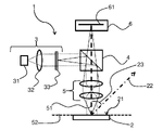
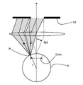
図1に、物体2の表面21の3Dトポグラフィ計測システム1の実施形態を示す。本システム1はパターン化照明源3を有しており、図示実施形態におけるパターン化照明源3は光源31例えば1個又は複数個のLEDと、コンデンサ光学系32と、パターンマスク33とを有している。物体2の表面21のパターン化照明は、パターンマスク33をその表面21上へと投射することで生成される。より精密に言えば、図示実施形態では光源31からの光が、コンデンサ32及びパターンマスク33を通過したあとビームスプリッタ4に到達し、その光のうち少なくとも一部分が、そのビームスプリッタ4により対物系5へと差し向けられそこを通過して物体2の表面21に到達する。その後、表面21からの光が、対物系5を通過してビームスプリッタ4に到達し、表面21からの光の一部分が、そのビームスプリッタ4により検出器61、例えば図示の如くカメラ6の一部たるそれへと差し向けられる。対物系5により規定される光軸51及び焦平面52のうち、光軸51は焦平面52に対し垂直である。投射されたパターンマスク33はその焦平面52内で最良合焦する。
FIG. 1 shows an embodiment of a 3D
検出器61の働きで表面21の画像複数枚が記録される一方、物体2・対物系5間相対運動が実行される。物体2・対物系5間相対運動の方向22は、光軸51に対しある斜め角23を有する方向である。その相対運動中に、物体2の表面21が対物系5の焦平面52を通過する。この図は本システム1の巨視図であるので、焦平面52が物体2の表面21と一致するように示されている。その表面21のうち焦平面内に存する部分は、検出器61の働きで記録された表面21の画像において、最良合焦に見える。相対運動の方向22と光軸51とが斜め角23をなしているため、パターン化照明のパターンが物体2の表面21に対し動くのに加え、同表面の画像中に記録されているパターンのコントラストが、方向22に沿った相対運動のコースを辿り表面21が焦平面52を通過するのにつれて変化する。結果として、表面21上の位置から記録される光強度は、複数枚の画像に含まれる諸画像間で変動する。この光強度変動から、表面21上の個別位置に係る高さ情報を得ることができる。完璧を期して言うなら、物体2・対物系5間相対運動は、例えば、物体2を動かすことでも、本システム1を動かすことでも、物体2及び本システム1の双方を動かすことでも果たすことができる。
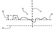
図2は物体2の表面21の一部分の模式的拡大図であり、表面21が全体としては平坦でなく構造、例えば隆起24に類するそれを有することが示されている。本発明に係る3Dトポグラフィ計測はそれらの構造の高さ25、ここでは隆起24に関し明示されているそれについて情報を得ることを、目的としている。隆起24の高さ25とは、いわば、基準面26に垂直な方向に沿った、その基準面26に対する隆起24の拡がりのことである。また、対物系5の光軸51及びそれに関連する焦平面52(図1参照)も示されている。本システム1内で物体2が正しく整列している場合、焦平面52は基準面26に対し平行となり、従って光軸51が焦平面52及び基準面26の双方に対し垂直となる。
FIG. 2 is a schematic enlarged view of a portion of the
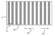
図3は物体2の表面21の頂面図であり、パターン化照明源3(図1参照)に発する投射パターン34が示されている。図示例では、また前出の図面によれば、物体2は対物系5に対し方向22に沿って動くので、その相対運動は基準面26内成分221を有するものとなる。結果として、パターン34は、物体2の表面21に対し、成分221とは逆の方向35に動く。これは、その相対運動中に、表面21上の所与位置に入射する光の強度が変化するであろうこと、並びに、その結果、その位置から記録される光強度が、カメラ6により記録される表面21の画像間で変化するであろうことを暗示している。
FIG. 3 is a top view of
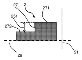
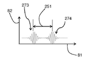
図4aは物体2、基準面26、並びに対物系5の光軸51(図1参照)を示すものであり、その光軸51が基準面26に対し垂直になっている。物体2は部分271及び272を有しており、基準面26に対するそれらの高さ値がある量251だけ相違しているため物体2が段差27を呈している。図4bには、対応する強度信号であり本発明に係る方法により得られたものが、ダイアグラムの態で示されている。このダイアグラム中、横軸81は物体2の光軸51沿い位置に相当しており、縦軸82は相対運動中に物体2上の位置から記録された光強度、より精密には段差位置からのそれに相当している。その光強度は2個の顕著な変調部分273及び274を呈している。想定上、図示ケースでは横軸81沿い値の増大が物体の対物系方向への移動に相当しているので、部分271(部分272より高背で対物系に近い部分)が対物系焦平面を通過した結果として変調部分273が生じ、部分272が対物系焦平面を通過した結果として変調部分274が生じる。変調部分273及び274の最大値が横軸81上で占める位置の差が、物体2の部分271・272間の高さ差251に相当する。光強度の高周波変調分、とりわけ変調部分273及び274中に見られるそれは、パターンと物体・対物系間相対運動との複合効果によりもたらされたものである。例えばパターンがラインパターン(線状パターン)である場合、そのパターンを構成している輝線及び暗線が図4aの物体2の段差27上方を通過する結果として、そうした高周波変調分がもたらされる。他方で、それら高周波変調分の振幅は、物体の表面上、より精密には物体2の部分271及び272それぞれの上での、そのラインパターンのコントラストにより決まる。コントラストが最高、ひいては高周波変調分の振幅が最大になるのは、部分271又は272それぞれが対物系5の焦平面52内に存しているときである(図1及び図2参照)。
4a shows the
図5に、本発明に係る方法にて用いうる照明ブランチ向け光学的構成を示す。図1と違いビームスプリッタ及びカメラは示されていない。本発明にとり精密な高さ計測が本質的なものであるので、図5に示した光学的構成を用い、この分野における計測の不確定性及び改善余地について論ずることにする。 FIG. 5 shows an optical configuration for the illumination branch that can be used in the method according to the invention. Unlike FIG. 1, beam splitters and cameras are not shown. Since precise height measurement is essential to the present invention, the optical configuration shown in FIG. 5 will be used to discuss measurement uncertainties and opportunities for improvement in this area.
図1と同じく、光源31、コンデンサ32、格子33、対物系5及びその光軸51、並びに物体2の表面21が示されている。対物系5は、撮像数値開口(撮像NA)54を規定する瞳53を有している。照明NA36も示されている。
As in FIG. 1,
以下の議論のため、ガウス座標系、光軸51沿い座標z、並びにそれに対し垂直な座標xを導入することにする。
For the following discussion, we will introduce a Gaussian coordinate system, a coordinate z along the
光軸51に対し垂直な任意の平面では、その平面上に投射された格子の画像の強度Iを、
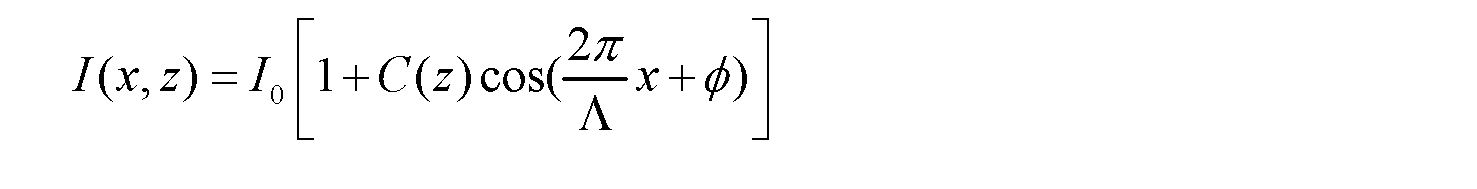
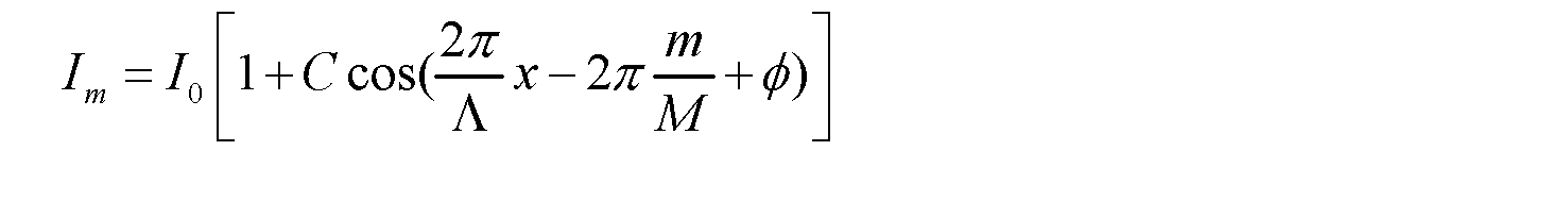
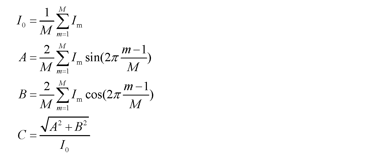
ここで、C(z)はzの関数たる強度変調振幅を指し示しており、Λは格子ピッチ、即ち格子33の隣接2ライン間距離であり、Φは位相オフセットである。コントラストを計測するため、また最終的には変調部分例えば図4bに示した273及び274の最大値を判別するため、図3中の矢印35からもわかるようにフリンジパターンをx方向にシフトさせ、またそれを本発明に係る方法に従い物体・対物系間の相対運動の斜め角により達成する。格子ピッチ1個分の距離に亘りこうしたフリンジパターンシフトがM回実行されるのであり、これは即ち、相対運動により格子ピッチ1個分だけパターンをシフトさせる間にM枚の画像が記録されるということである。対応する強度値は例えば
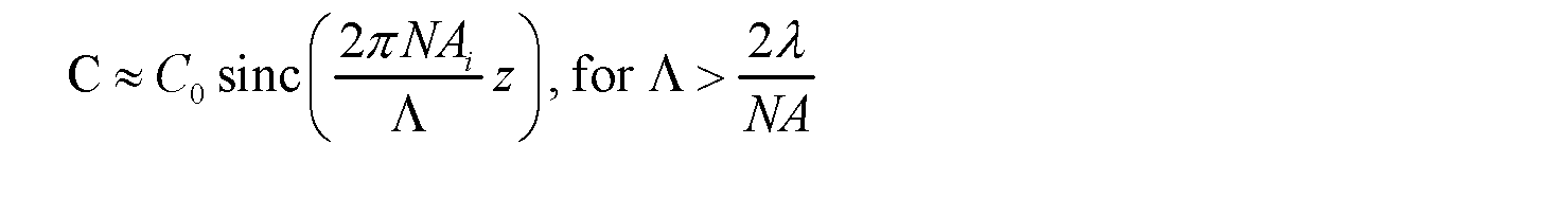
例えば一次元正弦格子が用いられている場合、zの関数たる格子投射画像のコントラストは、ほぼ
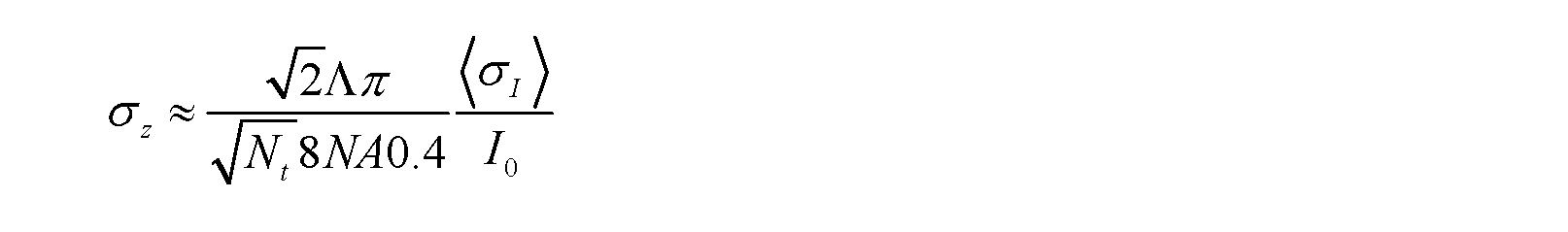
誤差伝搬論によれば、フリンジコントラストの分散に関する次の式
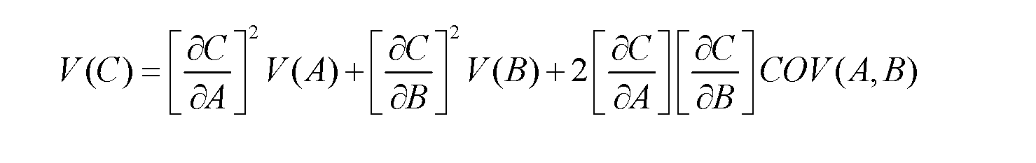
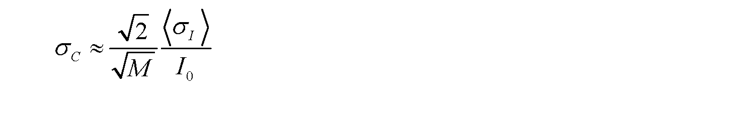
ここで、<σi>は画素強度の平均ノイズであり、<σi>/I0は、センサノイズ制限ケースでは検出器ダイナミックレンジの逆数、ショットノイズ制限ケースではセンサのフルウェルキャパシティの平方根の逆数となる。 where <σ i > is the average noise of the pixel intensity and <σ i >/I 0 is the reciprocal of the detector dynamic range for the sensor noise limited case and the square root of the sensor full well capacity for the shot noise limited case. is the reciprocal of
ピークの64%における焦点応答の勾配を用いることで計測再現性を推定し、
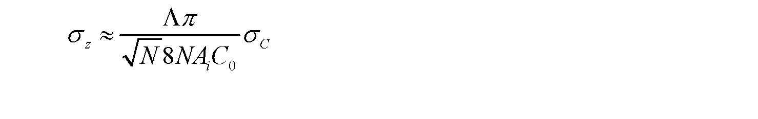
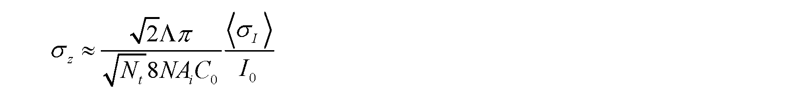
この誤差伝搬モデルの開発目標は、光学系パラメタが根底レベルでどのように性能に影響するかを示すことであるので、機械運動誤差及びセンサノイズが無視される理想条件下でモデルが導出される。そのモデルは最良ケースシナリオを表すものとなる。計測再現性に関する前出の等式により示される通り、
1.格子ピッチ(Λ)を小さくすること
2.フリンジコントラスト(C0)を高めること
3.光学系により制限される照明数値開口(NAi)を高めること
4.センサにより制限される画像ダイナミックレンジの逆数を大きくすること
5.データレート及びスループットにより制限される計測回数を増やすこと
で、計測再現性を改善することができる。
Since the goal of developing this error propagation model is to show how optical system parameters affect performance at the underlying level, the model is derived under ideal conditions where mechanical motion errors and sensor noise are neglected. . The model will represent the best case scenario. As indicated by the previous equation for measurement reproducibility,
1. 1. Reduce the grating pitch (Λ). 3. Enhancing fringe contrast (C 0 ). 4. Increasing the illumination numerical aperture (NA i ) limited by the optical system. 4. Increase the reciprocal of the image dynamic range limited by the sensor. Measurement reproducibility can be improved by increasing the number of measurements limited by data rate and throughput.
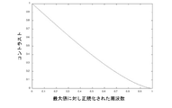
そのため、格子ピッチを小さくし格子コントラストを高めることが望まれる。しかしながら、円形アパーチャを有する非コヒーレント撮像システムの光学的伝達関数に関し図6に示されているように、格子ピッチを小さくするとフリンジコントラストが低まるので、格子ピッチ及びフリンジコントラストは一般に相容れない二条件とされる。図6では、格子ピッチが、使用最高空間周波数に対し正規化された、格子の空間周波数として示されている。空間周波数が高いということは単位長当たり格子ライン本数が多いということ、従ってその格子の隣接ライン間距離即ち格子ピッチが小さいということである。 Therefore, it is desirable to reduce the grating pitch and increase the grating contrast. However, as shown in FIG. 6 for the optical transfer function of a non-coherent imaging system with a circular aperture, grating pitch and fringe contrast are generally regarded as mutually exclusive terms, since reducing grating pitch reduces fringe contrast. be. In FIG. 6 the grating pitch is shown as the spatial frequency of the grating normalized to the highest spatial frequency used. A high spatial frequency means that the number of grid lines per unit length is large, and therefore the distance between adjacent lines of the grid, that is, the grid pitch is small.
非コヒーレント照明に関しては、格子ピッチの関数たるフリンジコントラストが

格子ピッチの関数たる計測再現性誤差は、これらの等式とσzに関する前出の等式とを組み合わせることで得られるものであり、その結果が図7中にプロットされている。最適格子ピッチは遮断ピッチΛminの2倍より僅かに大きいので、簡略化のため
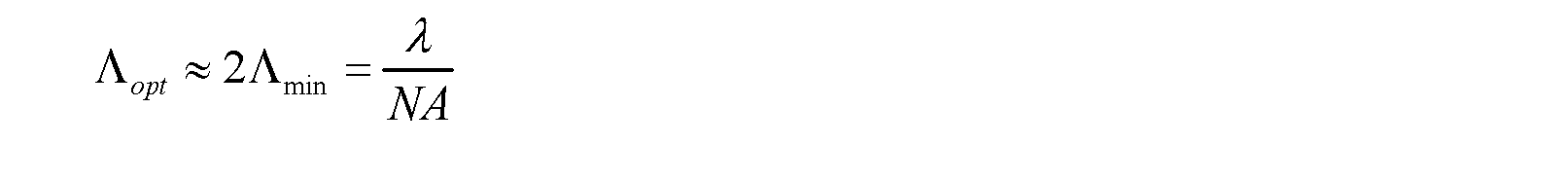
従って、フルNA照明及びショットノイズ制限ケースでは、計測再現性が
また、ショットノイズ制限ケースにおいては

ここに、Neは撮像センサのフルウェルキャパシティを表している。これは最良シナリオケースであり、計測性能の基本限界を示している。実際の計測は機械ノイズ、主としてz方向位置決めの安定性に由来するそれにより、往々にして制限される。 Here, N e represents the full well capacity of the imaging sensor. This is a best-case scenario and represents a fundamental limit of metrology performance. Practical measurements are often limited by machine noise, primarily due to z-positioning stability.
図6から看取しうるように、最適格子ピッチでの(遮断周波数の半分での)投射格子コントラストは約40%であり、これは非コヒーレント撮像システムの変調伝達関数(MTF)により与えられている。この低コントラストは、その上に格子が投射される物体平面における、諸回折成分の不平衡ミキシングの結果である。このことが図8及び図9に子細に描かれている。 As can be seen from FIG. 6, the projected grating contrast (at half the cutoff frequency) at the optimum grating pitch is about 40%, which is given by the modulation transfer function (MTF) of the non-coherent imaging system. there is This low contrast is the result of unbalanced mixing of the diffraction components at the object plane onto which the grating is projected. This is depicted in detail in FIGS. 8 and 9. FIG.
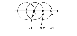
図8に、コンデンサ32、格子33、光軸51及び瞳53を有する対物系5、並びに物体2を示す。焦点深度28や、物体2上に投射され出現する格子ピッチ331も示されている。0次、+1及び-1なる指示子は、0次回折成分と二通りの1次回折成分とを指し示している。ここでは、格子のピッチが、照明用光波長を瞳53の数値開口で除したものに等しい旨、仮定している。
FIG. 8 shows objective 5 with
図9に示すように、図8の装備では、照明瞳上のどの所与点でも二通りある1次回折成分のうち一方だけ(即ち+1次か-1次)がその光学系を通過し、他方は回折されてその瞳外に出る。従って、物体2の表面上に格子33の画像を形成するのは、0次回折成分と+1次回折成分、或いは0次回折成分と-1次回折成分であり、それらの干渉により格子の画像が再現される。標準的な格子では一方の1次回折光の強度が0次回折光の強度よりも低いので、得られる格子画像は低コントラストになる。
As shown in FIG. 9, in the arrangement of FIG. 8, at any given point on the illumination pupil, only one of the two first order diffraction components (i.e. +1st or -1st) passes through the system, The other is diffracted and exits the pupil. Therefore, it is the 0th and +1st order diffraction components, or the 0th and -1st order diffraction components that form the image of the grating 33 on the surface of the
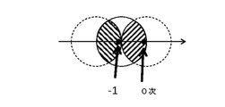
図10にコントラストの改善方法を示す。図示されているのはコンデンサ32、格子33、対物系5及びその瞳53、並びに物体2である。焦点深度28や、物体2上に現れる格子ピッチ331も、指し示されている。ここでは、格子33のピッチが照明用光波長を瞳53の数値開口で除したものに等しいものと仮定している。この格子33は、0次回折成分と一方の1次回折成分のみ、ここでは-1次回折成分のみをもたらすよう、またそれら0次回折成分及び一方の1次回折成分が等強度となるようなものである。これは例えばブレーズド格子により達成することができる。
FIG. 10 shows a method of improving contrast. Shown are
図11に示すように、図10の装備では、格子画像が0次回折成分の干渉、図示例なら-1次回折成分との干渉により形成される。図10の装備ではこれら二通りの回折成分が等強度となるので、得られる格子画像は、図9に示した状況に比べ、そのコントラストが改善されたものとなる。実際、コントラストを100%まで改善させることができ、対応する計測精度の2倍以上の改善へと導くことができる。図10の装備には幾通りかの改変が可能であり、例えば軸外アパーチャにすることができる。 As shown in FIG. 11, in the setup of FIG. 10, the grating image is formed by the interference of the 0th order diffraction component, in the example shown, the −1st order diffraction component. Since these two diffraction components are of equal intensity in the setup of FIG. 10, the resulting grating image has improved contrast compared to the situation shown in FIG. In fact, contrast can be improved by up to 100%, leading to a corresponding improvement in measurement accuracy of more than a factor of two. Several modifications are possible to the arrangement of FIG. 10, for example an off-axis aperture.
注記すべきことに、このコントラスト改善は、焦点深度の伸長と引き替えに得られたものではない。図8及び図10に示すように、格子コントラストが最大値の半分まで劣化する最良合焦位置からの距離として定義される幾何学的な焦点深度は、図8に示す如き非コヒーレント照明の場合でも、また図10に示した部分コヒーレント軸外照明でも、おおよそΛ/NAとなる。例えば、照明数値開口NAiが撮像数値開口NAよりもかなり小さい近コヒーレント照明では、フリンジピッチをλ/(2NA)なる最小値(最高空間周波数に対応)にすることができ、その上でなおフリンジコントラストを100%にすることができる。投射された格子のコントラストが、実質的に無限大の焦点範囲に亘り100%に保たれるシステムは、鏡面反射面上で高さ感度を呈さないであろう。 It should be noted that this contrast improvement is not obtained at the expense of extending the depth of focus. As shown in FIGS. 8 and 10, the geometric depth of focus, defined as the distance from the best focus position at which the grating contrast degrades to half its maximum value, is , and even with the partially coherent off-axis illumination shown in FIG. 10, approximately Λ/NA. For example, in near-coherent illumination, where the illumination numerical aperture NAi is much smaller than the imaging numerical aperture NA, the fringe pitch can be a minimum value (corresponding to the highest spatial frequency) of λ/(2NA) and still the fringes Contrast can be 100%. A system in which the projected grating contrast is maintained at 100% over a virtually infinite focus range will not exhibit height sensitivity on specular surfaces.
図12に、物体2の表面21の3Dトポグラフィ計測システム100の実施形態を示す。本システム100はパターン化照明源3を有しており、図示実施形態におけるパターン化照明源3は、光源31例えば1個又は複数個のLEDと、コンデンサ光学系32と、パターンマスク33とを有している。本システム100は均一照明源7も有しており、図示実施形態における均一照明源7は、光源71例えば1個又は複数個のLEDと、コンデンサ光学系72とを有している。均一照明源7からの光及びパターン化照明源3からの光を共にビームスプリッタ4へと差し向けるための手段73、例えば半透明ミラーのようなビームスプリッタが設けられている。ビームスプリッタ4はその光のうち少なくとも一部分を対物系5内に差し向け、その光はその対物系5を介し物体2の表面21に到達する。更にその表面21からの光が対物系5内を通過してビームスプリッタ4に到達し、表面21からの光のうち一部分がそのビームスプリッタ4により検出器61、図示例ではカメラ6の一部たるそれへと差し向けられる。対物系5により光軸51及び焦平面52が定まり、その光軸51は焦平面52に対し垂直となる。物体2の表面21上には構造、とりわけ鏡面構造たりうるそれ、具体的には半田バンプ9であるそれが示されている。
FIG. 12 shows an embodiment of a 3D
光源31及び71を交互に動作させることにより、物体2の表面21の交互照明が行われる。光源71を動作、即ち発光させた場合、物体2の表面21の照明は均一になる。光源31を動作、即ち発光させた場合、物体2の表面21の照明がパターン化される。
Alternating illumination of the
物体2・対物系5間相対運動が実行されている間に、検出器61の働きで表面21の画像複数枚が記録される。それら複数枚の画像のうち幾枚かの画像は、表面21が均一照明にさらされている間に記録されたものであり、また当該複数枚の画像のうち幾枚かの画像は、表面21がパターン化照明にさらされている間に記録されたものである。この実施形態における物体2・対物系5間相対運動の方向22は光軸51に対し平行である。その相対運動中に、物体2の表面21は対物系5の焦平面52を通過する。この図は本システム100の巨視図であるので、焦平面52が一見して物体2の表面21と一致している。
Several images of the
図示実施形態では、図1の実施形態とは対照的に、相対運動方向22が対物系5の光軸51に対し平行であるため、物体2の表面21に対する投射パターンのシフトがない。図12の実施形態は、とりわけ、半田バンプ付の表面の検査を目的としている。通常、半田バンプは表面21上にアレイをなしてレイアウトされるが、図12には代表として単一の半田バンプ9が示されている。半田バンプ間エリアのうち、表面上に投射されたパターン例えば格子のピッチより半田バンプ間距離が大きいところでは、半田バンプ間表面の高さを、表面に対しパターンをシフトさせることなく投射パターンのコントラストから計測することができる。これは、従来技術では必要であったのと違い、光軸51に沿った物体2・対物系5間相対位置毎に複数枚の画像を記録する必要がないことを、暗示している。
In the illustrated embodiment, in contrast to the embodiment of FIG. 1, there is no shift of the projection pattern with respect to the
この実施形態では、半田バンプ9間表面高さが、パターン化照明下で記録された画像から求まる一方、半田バンプ9の高さが、均一照明下で記録された画像から求まる。
In this embodiment, the surface height between
考えるに、図12に示す実施形態ではパターン化照明源3及び均一照明源7がめいめいに光源を有しているが、これは本発明の限定事項ではない。パターン化照明源3及び均一照明源7で共通の光源が用いられる実施形態が考えられる。そうした場合には、相応な手段を設けてパターン化照明及び均一照明による物体表面の交互照明を実現すればよい。その手段を例えば伝送切替フィルタ群とし、光源からパターン化照明源,均一照明源それぞれに備わる他素子への光路が交互に遮断されるようにすることができる。各フィルタによる伝送を制御することで各照明源からの光の強度を制御することもできる。或いは、その手段を、光源から光を集めてパターン化照明源,均一照明源それぞれに備わる他素子へと交互に差し向けるものにしてもよい。
Considering that in the embodiment shown in FIG. 12 the patterned
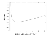
図13は半田バンプ9、ここでは半径rのそれが撮像される光学的状況を描いたものである。おわかり頂けるように、半田バンプ9が反射性でその表面が湾曲しているため、バンプ頂部の小部分しか撮像されえない。バンプ頂部のうち検出器にとり可視な部分のサイズは、照明数値開口及び撮像数値開口の双方に依存する。フル数値開口(NA)照明では、バンプ頂部のうち検出器にとり可視な部分の半値全幅半径がD=rNAにより与えられる。光学的NAを十分に高くし、十分な光学的分解能が得られるようにしないと、アレイレイアウト内の個別バンプを正確に計測することができない。通常、バンプレイアウトにおけるバンプ間隔対バンプ直径の比は1:1であるので、隣接バンプ間光学的クロストークを回避するには撮像点拡がり関数(PSF)をバンプ半径のオーダとする必要がある。最小NAは従って

そしてそれに対応するバンプ頂部可視部分の最小直径は

デバイストポグラフィ検査で典型的なNAは0.1~0.3付近であり、これは、視野サイズを大きくしてデバイス全体を撮像し更に高スループットを実現するため、ひいてはバンプ頂部の可視部分が光学的PSFより小さくなりその撮像システムでは点物体として扱えるようにするためである。この場合、焦点による撮像点拡がり関数の変化の仕方に密に追従することから、ピーク画素強度かバンプ頂部自体の画像のサイズかを高さ計測に用いることができる。 A typical NA for device topography inspection is around 0.1 to 0.3. This is because it is smaller than the target PSF and can be handled as a point object in the imaging system. In this case, since the way the imaging point spread function changes due to focus is closely followed, either the peak pixel intensity or the size of the image of the top of the bump itself can be used for height measurement.
図13に示すように、バンプ9の表面にある点Pがまだ瞳53を介した照明にさらされているのに、その点Pからの反射光が瞳53内を通らず、従って検出器61(図12参照)に到達しないことがある。この場合、半田バンプ9の表面の点Pを、検出器61により記録された画像中に見いだすことができない。図13からお察し頂くべきことに、こうして反射光が瞳53を通過し損ねる原因は、主に、その反射の鏡面的性質と併せ、バンプ9の表面の湾曲にある。
As shown in FIG. 13, although point P on the surface of
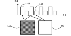
図14は図12に示したシステムの動作手順を示す図であり、図12中のパターン化照明源3及び均一照明源7により生成された交互照明が描かれている。同図の横軸は位置z、即ち方向22沿い運動中に対物系5(図12参照)の光軸51沿いで物体2がとる位置を表している。縦軸は、光源31,71それぞれにより放射された光の強度を表している。市松模様付の正方形143はパターン化照明源3の動作を象徴しており(パターンは市松模様に限られない)、無地の正方形147は均一照明源7の動作を象徴している。同図中でそれら正方形からバー144,148に向かっている矢印は、対応する照明源がアクティブになる光軸沿い運動段階を指し示している。即ち、パターン化照明源3がアクティブとなって照明を供給するのは、光軸51沿い運動段階のうち図中でバー144が示されている段階であり、均一照明源7がアクティブとなって照明を供給するのは、光軸51沿い運動段階のうち図中でバー148が示されている段階である。
FIG. 14 is a diagram showing the operating procedure of the system shown in FIG. 12, and depicts the alternating illumination produced by the patterned
バー144は、バー148により与えられる均一照明源7内光源71の強度に比べ、パターン化照明源3内光源31の強度の方が高いことを、指し示している。このことからわかるように、それら光源の強度を、表面21のうちそれぞれ計測が実行される部分の特性に適合させることができる。鏡面的な半田バンプに対する計測では、半田バンプ間表面に対する計測に比べ低めの強度が通常は適切である。
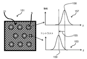
図15に、専ら例証目的で、均一照明下の半田バンプとパターン化照明下の半田バンプ間表面21との結合画像151を示す。2個のダイアグラムも示されている。ダイアグラム157は、z方向位置即ち光軸51に対し平行な方向22(図12参照)に沿った位置の関数として、半田バンプ9から記録された強度を示している。ダイアグラム153は、z方向位置の関数として、半田バンプ9間表面21から計測されたコントラストを示している。ダイアグラム157に示した強度はz方向位置158にて最大値を呈し、ダイアグラム153に示したコントラストはz方向位置159にて最大値を呈している。これらz方向位置158,159即ち対応する最大値が生じている位置は、それぞれ、半田バンプ9の頂部(最大値158),表面21(最大値159)が焦平面52(図12参照)を通過するz方向位置である。従って、それらz方向位置158・159間の差155が半田バンプ9の高さである。
For illustrative purposes only, FIG. 15 shows a combined
ダイアグラム153に入れるコントラスト値を決めるに当たっては、その投射パターンが検出器61(図12参照)の画素サイズにマッチする市松模様である場合、それらコントラスト値を最少で2×2個の画素から算出することができる。より広い画素エリア、即ちN×N個の画素エリア、但しN>2も用いうる。その選択は、通常、光軸51に対し垂直な方向の空間分解能条件及びバンプ9間距離により左右されよう。画素エリア拡大は算出されるコントラストの精度向上につながるが、明らかな通り、光軸51に対し垂直な方向の空間分解能低下にもつながる。
In determining the contrast values to be included in diagram 153, if the projected pattern is a checkerboard pattern that matches the pixel size of detector 61 (see FIG. 12), then these contrast values are calculated from a minimum of 2.times.2 pixels. be able to. Larger pixel areas, ie N×N pixel areas, where N>2, can also be used. The selection will usually depend on the spatial resolution conditions in the direction perpendicular to the
図16に、半田バンプのように小湾曲を有する表面に関し、本発明に係る方法における画素応答(例.検出器の対応画素により記録された光強度を表す画素値)を示す。同図の左側にある5枚の画像は、焦点165(画像のうち2枚のみに示す)に差し向けられ半球163(半田バンプ)の表面上に入射する光線164を、様々な半球163・焦点165間相対位置に関し示したものである。同図の右側では、画素応答が縦軸162上に示される一方、横軸161により半球163・焦点165間相対位置が示されている。矢印は、同図中の画素応答のうちどの部分が、左側にある5枚の画像のいずれに対応するのかを、指し示すものである。
FIG. 16 shows the pixel response (eg pixel value representing the light intensity recorded by the corresponding pixel of the detector) in the method according to the invention for a surface with a small curvature like a solder bump. The five images on the left side of the figure show a
読み取れるように、この画素応答は2個の最大値を有している。横軸161の値が小さな方の最大値は、左側画像のうち下から2枚目のものに示されているように、光線164の焦点165が半球163の頂部にある状況に相当している。計測中にこの状況が発生するのは、半田ボールの頂部が対物系5(図12参照)の焦平面52内にあるときである。2個目の最大値が生じるのは、左側画像のうち上から2枚目のものに示されているように、光線164の焦点165が半球163の中心に一致しているときである;実際には光線164が半球163内に入り込まずその表面で反射されることに留意されたい。計測実行時には物体2・対物系5間相対運動方向がわかっているので、半田ボール頂部であり焦平面52内にあるものにそれら2個のピークのうちいずれが対応するのかは明々白々である。他方のピークを用いることでバンプ頂部表面の湾曲を計測することができ、ひいてはそれを校正目的で用い計測の正確性を改善することができる。
As can be seen, this pixel response has two maxima. The smaller maximum value of the
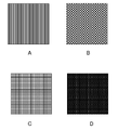
図17にパターン化照明生成用パターンマスクを数例示す。これらのパターンマスクは、図1に示したパターン化照明専用型の実施形態でも、図12に示したパターン化照明・均一照明交互型の実施形態でも、用いることができる。本発明はここに示した種類のパターンマスクに限定されない。図示されている具体例は正弦格子(A)、市松模様(B)、ライングリッド又はクロスライン格子(C)及びピンホールアレイ(D)である。 FIG. 17 shows several examples of pattern masks for generating patterned illumination. These pattern masks can be used in either the patterned illumination only embodiment shown in FIG. 1 or the alternating patterned and uniform illumination embodiment shown in FIG. The invention is not limited to pattern masks of the type shown here. Examples shown are sinusoidal grids (A), checkered patterns (B), line grids or cross-line grids (C) and pinhole arrays (D).
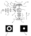
図18に、物体2の表面21の3Dトポグラフィ計測システム200の実施形態を示す。図示実施形態は図12に示した実施形態のシステム100と非常に類似しており、図18に現れている要素の大半は既に論じたものである。本システム200では、瞳マスク74が均一照明源7内に組み込まれている。瞳マスク74は照明アパーチャとして動作する。照明アパーチャにより、様々なフィーチャ形状について画像コントラスト及び焦点応答を改善することができる。図18には、瞳マスク74が採りうる形状について、2個の非限定的な例も示されている。瞳マスク例741はリングアパーチャ、瞳マスク例742は円形アパーチャである。
FIG. 18 shows an embodiment of a 3D
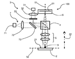
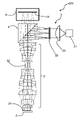
図19に、本発明に係るシステムの実施形態であり本発明を実行するのに用いうる光学モジュール300を示す。ここに示した光学モジュール300の構成は図1に示したシステム1の構成に類似しているが、図12のシステム100又は図18のシステム200の構成をベースにした光学モジュールも考えられる。
FIG. 19 shows an
パターン化照明源3は、光源31、コンデンサ32及びパターンマスク33を有している。パターン化照明源3からの光がビームスプリッタ4に到達すると、その光の一部分がそのビームスプリッタ4によって対物系5へと差し向けられ、そこから物体2へと到達した光により、物体2の表面21にパターン化照明が供給される。対物系5は瞳53を有している。表面21からの光は、対物系5及びビームスプリッタ4を通過した後、カメラ6内の検出器61に到達する。既に上述した通り、検出器61を用いることで、物体2及び対物系5の相対運動中に表面21の画像複数枚を記録することができる。
Patterned
モジュール300はコンパクト且つ単純であるので、複数物体並列検査での使用に適している。非常に具体的だがなお非限定的な例を提供するには、対物系5の視野直径を22mm、NAを0.2とし、通常は30nmであるLED照明波長帯幅向けにその対物系5を補正すればよい;通常は1個又は複数個のLEDが光源31として用いられるのでこうするのが望ましい。このNAは十分高いのでサブμmの計測精度を達成することができ、またその視野サイズにより検査対象物体の大抵のサイズをカバーすることができる。ビームスプリッタキューブ4の撮像側は照明路を撮像路から分岐させるところであり、レンズデザイン上一体部分となっている。これは、その対物レンズ及びチューブレンズが別体な従来の撮像顕微鏡、特に対物系・チューブレンズ間平行光化空間にて照明路及び撮像路が分岐されるため格子投射に更なるチューブレンズが必要であった従来の撮像顕微鏡に比べて、かなり単純且つコンパクトなデザインである。このデザインのもう一つの長所は、パターンマスク33及び検出器61がきっちりと共役平面に存しているため、残留視野歪みがキャンセルされ投射パターンのサンプリングエイリアシングがなくなることである。このデザインは物体側,像側の双方でテレセントリックでもあるので、スルーフォーカス信号歪みを抑えることができる。
The compactness and simplicity of the
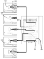
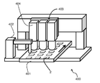
図20に、複数個の物体2を並列検査するシステム400を示す。物体2はピックアンドプレース装置402によりコンベア401上に載置される。コンベア401は物体2を検査モジュール404の配列403へ、またその先へと搬送するものであり、図示具体例に係るシステム400は3個の検査モジュール404を有している。各物体2は1個の検査モジュール404により検査される。各検査モジュール404は、自分が検査する物体2それぞれを対象に本発明に係る方法を実行する。検査対象物体2の個数及びスループット条件次第で検査モジュール404の個数を変えうるよう、即ち検査モジュール404を本システム400に追加し又はそこから除去することができるよう、本システム400を構成することも考えられる。
FIG. 20 shows a
各検査モジュール404は、例えば図19に記したモジュール300とすればよいが、例えば図1にて論じたシステム1、図12にて論じたシステム100或いは図18にて論じたシステム200としてもよい。検査モジュール404は、総じて、図1~図19の文脈で論じた発明に係るシステムのいずれとしてもよく、また本発明に係る方法を実行するよう構成されたどのようなシステムであってもよい。検査モジュール404にて、パターン化照明及び物体・対物系間の相対運動に依拠していてその相対運動の方向と対物系の光軸とがある斜め角をなす発明に係る方法を用いてもよいし、或いはパターン化照明及び均一照明を交互に利用する発明に係る方法を用いてもよい。
Each
上掲の記述では、本発明の諸実施形態についての全般的理解を促すため数多くの具体的細部が提示されている。しかしながら、本発明の図示諸実施形態についての上掲の記述は、排他的な趣旨や被開示形態そのものに本発明を限定する趣旨のものではない。関連分野に習熟した者(いわゆる当業者)であれば、そうした具体的細部のうち1個以上を欠き或いは他の方法、部材等々で以て本発明を実施しうることを、認識されるであろう。また例えば、本発明の諸態様が不明瞭になることを避けるため、周知な構造や動作については図示又は詳細記述していない。本発明の具体的実施形態及び諸例を例証目的で本願中に記述したが、いわゆる当業者にはご認識頂けるように、本発明の技術的範囲内で様々な等価的修正を行うことができる。 In the above description, numerous specific details are presented to facilitate a general understanding of the embodiments of the invention. However, the above description of illustrated embodiments of the invention is not intended to be exclusive or to limit the invention to the precise forms disclosed. It will be appreciated by those skilled in the relevant art (that is, those skilled in the art) that the invention may be practiced without one or more of the specific details, or with other methods, materials, and so on. deaf. In other instances, well-known structures and operations have not been shown or described in detail to avoid obscuring aspects of the invention. Although specific embodiments and examples of the invention have been described herein for purposes of illustration, various equivalent modifications can be made within the scope of the invention, as will be recognized by those skilled in the art.
それらの修正は、上掲の詳細記述に照らし、本発明に施すことができる。後掲の特許請求の範囲中で用いられている語を以て、本発明が明細書及び特許請求の範囲中で開示された具体的実施形態に限定されるものと解すべきではない。寧ろ、本発明の技術的範囲は後掲の特許請求の範囲により決定づけられるべきものであり、また特許請求の範囲は特許請求の範囲の解釈についての確立された理論に従い解釈されるべきものである。 Those modifications can be made to the invention in light of the above detailed description. The language used in the following claims should not be construed as limiting the invention to the specific embodiments disclosed in the specification and claims. Rather, the scope of the invention is to be determined by the following claims, which are to be construed in accordance with established doctrines of claim interpretation. .
1 システム、2 物体、21 物体の表面、22 相対運動方向、221 相対運動の成分、23 斜め角、24 隆起、25 高さ、251 高さ差、27 段差、271 表面の一部分、272 表面の一部分、273 光強度の一部分、274 光強度の一部分、26 基準面、28 焦点深度、3 パターン化照明源、31 光源、32 コンデンサ、33 パターンマスク、331 格子ピッチ、34 パターン、35 表面に対するパターンの運動方向、36 照明アパーチャ、4 ビームスプリッタ、5 対物系、51 光軸、52 焦平面、53 瞳、54 撮像アパーチャ、6 カメラ、61 検出器、7 均一照明源、71 光源、72 コンデンサ、73 手段(ビーム分割)、74 瞳(照明アパーチャ)、741 リングアパーチャ、742 円形アパーチャ、81 横軸、82 縦軸、9 半田ボール、100 システム、143 市松模様正方形、144 バー、147 無地正方形、148 バー、151 結合画像、153 ダイアグラム、155 高さ差、157 ダイアグラム、158 最大値(強度)、159 最大値(コントラスト)、161 横軸、162 縦軸、163 半球、164 光線、165 焦点、200 システム、300 モジュール、400 システム、401 コンベア、402 ピックアンドプレース装置、403 (検査モジュールの)配列、404 検査モジュール、A,B,C,D パターンマスク例、Dmin 半田ボール頂部の可視部分の最小直径、P 半田ボール表面上の点。
1 system, 2 body, 21 surface of body, 22 direction of relative motion, 221 component of relative motion, 23 oblique angle, 24 elevation, 25 height, 251 height difference, 27 step, 271 part of surface, 272 part of surface , 273 fraction of light intensity, 274 fraction of light intensity, 26 reference plane, 28 depth of focus, 3 patterned illumination source, 31 light source, 32 condenser, 33 pattern mask, 331 grating pitch, 34 pattern, 35 motion of pattern relative to surface. direction, 36 illumination aperture, 4 beam splitter, 5 objective, 51 optical axis, 52 focal plane, 53 pupil, 54 imaging aperture, 6 camera, 61 detector, 7 uniform illumination source, 71 light source, 72 condenser, 73 means ( beam splitting), 74 pupil (illumination aperture), 741 ring aperture, 742 circular aperture, 81 horizontal axis, 82 vertical axis, 9 solder ball, 100 system, 143 checkered square, 144 bar, 147 plain square, 148 bar, 151 Combined Image, 153 Diagram, 155 Height Difference, 157 Diagram, 158 Maximum (Intensity), 159 Maximum (Contrast), 161 Horizontal Axis, 162 Vertical Axis, 163 Hemisphere, 164 Ray, 165 Focus, 200 System, 300 Module , 400 System, 401 Conveyor, 402 Pick and Place Equipment, 403 Array (of Inspection Modules), 404 Inspection Module, A, B, C, D Pattern Mask Example, D min Minimum Diameter of Visible Part of Solder Ball Top, P Solder A point on the ball surface.
Claims (12)
パターン化照明源と、
均一照明源と、
前記パターン化照明及び前記均一照明双方を前記物体の表面に差し向けるよう配置された対物系と、
前記対物系を介し前記物体の表面の画像を複数枚記録するよう配置及び構成された検出器と、
前記検出器に接続され、前記複数枚の画像のうち、前記パターン化照明下で記録された画像の光強度差、及び前記均一照明下で記録された画像の光強度差に基づき前記物体の表面の位置の高さ情報を決定するように構成されたコンピュータと、
を備え、前記光強度は、前記物体の光軸に沿った1つの方向に沿って変化する、
システム。 An optical three-dimensional topography metrology system for the surface of an object, comprising:
a patterned illumination source;
a uniform illumination source;
an objective positioned to direct both the patterned illumination and the uniform illumination onto the surface of the object;
a detector arranged and configured to record multiple images of the surface of the object through the objective;
connected to the detector, the surface of the object based on the light intensity difference of the image recorded under the patterned illumination and the light intensity difference of the image recorded under the uniform illumination among the plurality of images; a computer configured to determine height information for the location of the
wherein the light intensity varies along one direction along the optical axis of the object;
system.
前記パターン化照明源が光源及びパターンマスクを有するシステム。 The system of claim 1, wherein
A system wherein the patterned illumination source comprises a light source and a pattern mask.
前記パターンマスクが市松模様又はピンホールアレイを有するシステム。 3. The system of claim 2, wherein
A system wherein said pattern mask comprises a checkerboard pattern or a pinhole array.
前記パターンマスクが格子であるシステム。 3. The system of claim 2, wherein
A system wherein said pattern mask is a grid.
前記格子が振幅格子又は位相格子であるシステム。 5. The system of claim 4, wherein
A system wherein the grating is an amplitude grating or a phase grating.
前記格子がライン格子又は正弦格子又はクロスライン格子であるシステム。 5. The system of claim 4, wherein
A system wherein said grid is a line grid or a sinusoidal grid or a crossline grid.
前記格子がブレーズド格子であるシステム。 5. The system of claim 4, wherein
A system wherein said grating is a blazed grating.
前記対物系・前記検出器間の撮像路と、少なくとも前記パターン化照明源・前記対物系間の照明路と前記均一照明源・前記対物系間の照明路のいずれか1つとが、ビームスプリッタを通過する形態で、前記ビームスプリッタが配置されているシステム。 The system of claim 1, wherein
an imaging path between the objective system and the detector, and at least one of an illumination path between the patterned illumination source and the objective system and an illumination path between the uniform illumination source and the objective system, each of which includes a beam splitter. A system wherein said beamsplitter is arranged in a pass-through configuration.
前記パターン化照明源・前記対物系間の照明路と前記均一照明源・前記対物系間の照明路の双方が、前記ビームスプリッタを通過するシステム。 9. The system of claim 8, wherein
A system in which both the patterned illumination source-to-objective illumination path and the uniform illumination source-to-objective illumination path pass through the beamsplitter.
前記パターンマスク及び前記検出器が共役平面内に存するシステム。 3. The system of claim 2, wherein
A system in which the pattern mask and the detector lie in conjugate planes.
前記物体と前記対物系の相対運動の方向が前記対物系の光軸に対し平行であるシステム。 The system of claim 1, wherein
A system wherein the direction of relative motion of said object and said objective is parallel to the optical axis of said objective.
Applications Claiming Priority (2)
| Application Number | Priority Date | Filing Date | Title |
|---|---|---|---|
| US201662289889P | 2016-02-01 | 2016-02-01 | |
| US62/289,889 | 2016-02-01 |
Related Parent Applications (1)
| Application Number | Title | Priority Date | Filing Date |
|---|---|---|---|
| JP2018559667A Division JP6846441B2 (en) | 2016-02-01 | 2016-11-04 | Optical 3D topography measurement system for the surface of an object |
Publications (2)
| Publication Number | Publication Date |
|---|---|
| JP2021081446A JP2021081446A (en) | 2021-05-27 |
| JP7166375B2 true JP7166375B2 (en) | 2022-11-07 |
Family
ID=59500792
Family Applications (2)
| Application Number | Title | Priority Date | Filing Date |
|---|---|---|---|
| JP2018559667A Active JP6846441B2 (en) | 2016-02-01 | 2016-11-04 | Optical 3D topography measurement system for the surface of an object |
| JP2021031926A Active JP7166375B2 (en) | 2016-02-01 | 2021-03-01 | Optical three-dimensional topography measurement system for the surface of an object |
Family Applications Before (1)
| Application Number | Title | Priority Date | Filing Date |
|---|---|---|---|
| JP2018559667A Active JP6846441B2 (en) | 2016-02-01 | 2016-11-04 | Optical 3D topography measurement system for the surface of an object |
Country Status (12)
| Country | Link |
|---|---|
| US (2) | US10634487B2 (en) |
| EP (2) | EP3411695B1 (en) |
| JP (2) | JP6846441B2 (en) |
| KR (1) | KR102668017B1 (en) |
| CN (2) | CN108603848B (en) |
| ES (1) | ES2908695T3 (en) |
| MY (2) | MY196634A (en) |
| PH (1) | PH12018501598A1 (en) |
| PT (1) | PT3411695T (en) |
| SG (2) | SG10201912769PA (en) |
| TW (2) | TWI723129B (en) |
| WO (1) | WO2017136011A2 (en) |
Families Citing this family (15)
| Publication number | Priority date | Publication date | Assignee | Title |
|---|---|---|---|---|
| JP6189984B2 (en) * | 2016-02-12 | 2017-08-30 | Ckd株式会社 | 3D measuring device |
| NL2020619B1 (en) * | 2018-01-16 | 2019-07-25 | Illumina Inc | Dual optical grating slide structured illumination imaging |
| KR102066129B1 (en) * | 2018-09-21 | 2020-01-14 | 한양대학교 산학협력단 | Apparatus and method for 3d information using dot array |
| US10704094B1 (en) | 2018-11-14 | 2020-07-07 | Element Biosciences, Inc. | Multipart reagents having increased avidity for polymerase binding |
| KR102008890B1 (en) | 2019-01-25 | 2019-08-08 | 단국대학교 산학협력단 | Method of measuring 3d profile |
| KR102260563B1 (en) * | 2019-07-02 | 2021-06-07 | 한국과학기술연구원 | Structure illumination microscope-based on checkerboard pattern |
| US10921721B1 (en) * | 2019-09-13 | 2021-02-16 | Applied Materials, Inc. | Measurement system and grating pattern array |
| US11060138B1 (en) | 2020-01-17 | 2021-07-13 | Element Biosciences, Inc. | Nucleic acid sequencing systems |
| DE102020201536A1 (en) * | 2020-02-07 | 2021-08-12 | Fraunhofer-Gesellschaft zur Förderung der angewandten Forschung eingetragener Verein | Method and device for contactless measurement of an object surface |
| CN111721231B (en) * | 2020-06-03 | 2021-11-19 | 华东师范大学 | Plant ecological monitoring system based on optical frequency comb |
| US20230280282A1 (en) * | 2020-07-13 | 2023-09-07 | Camtek Ltd. | Continuous bump measurement height metrology |
| WO2022013703A1 (en) * | 2020-07-13 | 2022-01-20 | Camtek Ltd. | Continuous bump measurement height metrology |
| AU2022316142A1 (en) | 2021-07-21 | 2024-02-22 | Element Biosciences, Inc. | Optical systems for nucleic acid sequencing and methods thereof |
| US12169920B2 (en) | 2022-01-05 | 2024-12-17 | Honeywell Federal Manufacturing & Technologies, Llc | Telecentric detection of lattice breakdown |
| CN121048525A (en) * | 2025-08-21 | 2025-12-02 | 苏州明鉴传感科技有限公司 | Mask-based bright-field 3D reconstruction apparatus and method |
Citations (2)
| Publication number | Priority date | Publication date | Assignee | Title |
|---|---|---|---|---|
| JP2011523057A (en) | 2008-06-05 | 2011-08-04 | トラスティーズ オブ ボストン ユニバーシティ | System and method for generating an optically sectioned image using both structured and uniform illumination |
| US20140376064A1 (en) | 2013-06-21 | 2014-12-25 | 3Shape A/S | Scanning apparatus with patterned probe light |
Family Cites Families (39)
| Publication number | Priority date | Publication date | Assignee | Title |
|---|---|---|---|---|
| US6249335B1 (en) * | 1992-01-17 | 2001-06-19 | Nikon Corporation | Photo-mask and method of exposing and projection-exposing apparatus |
| US5248876A (en) * | 1992-04-21 | 1993-09-28 | International Business Machines Corporation | Tandem linear scanning confocal imaging system with focal volumes at different heights |
| US5471303A (en) * | 1994-04-29 | 1995-11-28 | Wyko Corporation | Combination of white-light scanning and phase-shifting interferometry for surface profile measurements |
| JPH11211439A (en) * | 1998-01-22 | 1999-08-06 | Takaoka Electric Mfg Co Ltd | Surface profile measuring device |
| AU3991799A (en) * | 1998-05-14 | 1999-11-29 | Metacreations Corporation | Structured-light, triangulation-based three-dimensional digitizer |
| GB9901365D0 (en) * | 1999-01-22 | 1999-03-10 | Isis Innovations Ltd | Confocal microscopy apparatus and method |
| US6268923B1 (en) | 1999-10-07 | 2001-07-31 | Integral Vision, Inc. | Optical method and system for measuring three-dimensional surface topography of an object having a surface contour |
| FI20001568L (en) * | 2000-06-30 | 2001-12-31 | Thermo Radiometrie Oy | Defining surface shapes |
| US6724489B2 (en) * | 2000-09-22 | 2004-04-20 | Daniel Freifeld | Three dimensional scanning camera |
| US6870609B2 (en) | 2001-02-09 | 2005-03-22 | August Technology Corp. | Confocal 3D inspection system and process |
| US20020145734A1 (en) | 2001-02-09 | 2002-10-10 | Cory Watkins | Confocal 3D inspection system and process |
| US6893800B2 (en) | 2002-09-24 | 2005-05-17 | Agere Systems, Inc. | Substrate topography compensation at mask design: 3D OPC topography anchored |
| US7126699B1 (en) | 2002-10-18 | 2006-10-24 | Kla-Tencor Technologies Corp. | Systems and methods for multi-dimensional metrology and/or inspection of a specimen |
| US7286246B2 (en) * | 2003-03-31 | 2007-10-23 | Mitutoyo Corporation | Method and apparatus for non-contact three-dimensional surface measurement |
| DE10321888A1 (en) * | 2003-05-07 | 2004-12-02 | Universität Stuttgart | 3D optical metrology method in which a structured pattern is generated on an object surface and resultant virtual pixels measured with a white-light interferogram |
| US7680013B2 (en) * | 2005-11-29 | 2010-03-16 | Canon Kabushiki Kaisha | Optical information recording and reproducing apparatus |
| JP2008003520A (en) * | 2006-06-26 | 2008-01-10 | Toshiba Corp | Photomask and semiconductor device manufacturing method |
| JP4991872B2 (en) * | 2006-11-01 | 2012-08-01 | インフェーズ テクノロジィズ インコーポレイテッド | Configuration of monocular holographic data storage system |
| CN102802529B (en) * | 2009-06-16 | 2015-09-16 | 皇家飞利浦电子股份有限公司 | For the bearing calibration of differential contrast imaging |
| CA2763826C (en) * | 2009-06-17 | 2020-04-07 | 3Shape A/S | Focus scanning apparatus |
| US8754936B2 (en) * | 2009-07-03 | 2014-06-17 | Koh Young Technology Inc. | Three dimensional shape measurement apparatus |
| KR101121982B1 (en) * | 2009-07-03 | 2012-03-09 | 주식회사 고영테크놀러지 | Three dimensional shape measuring apparatus |
| EP2327956B1 (en) * | 2009-11-20 | 2014-01-22 | Mitutoyo Corporation | Method and apparatus for determining the height of a number of spatial positions on a sample |
| JP5942847B2 (en) * | 2010-05-07 | 2016-06-29 | 株式会社ニコン | Height measuring method and height measuring apparatus |
| EP2437027A3 (en) * | 2010-10-03 | 2012-05-30 | Confovis GmbH | Device and method for three dimensional optical mapping of a sample |
| US8649024B2 (en) * | 2010-12-03 | 2014-02-11 | Zygo Corporation | Non-contact surface characterization using modulated illumination |
| US10048480B2 (en) * | 2011-01-07 | 2018-08-14 | Zeta Instruments, Inc. | 3D microscope including insertable components to provide multiple imaging and measurement capabilities |
| US8610902B2 (en) | 2011-06-02 | 2013-12-17 | Asm Technology Singapore Pte Ltd | Apparatus and method for inspecting an object with increased depth of field |
| DE102012017922B4 (en) * | 2012-09-11 | 2024-03-14 | Carl Zeiss Microscopy Gmbh | Optical arrangement and light microscope |
| US9255791B2 (en) * | 2012-09-28 | 2016-02-09 | The Board Of Trustees Of The University Of Illinois | Optically monitoring and controlling nanoscale topography |
| CN104180773B (en) * | 2013-05-20 | 2017-07-21 | 沈阳同联集团高新技术有限公司 | A kind of apparatus for measuring three-dimensional profile |
| CN103292740B (en) * | 2013-05-24 | 2016-04-13 | 贵阳嘉瑜光电科技咨询中心 | A kind of 3-D scanning instrument measurement method and device thereof |
| CN103424795B (en) * | 2013-09-03 | 2015-10-28 | 苏州大学 | A kind of reflective spectro-grating and interference lithography system |
| TWI489101B (en) * | 2013-12-02 | 2015-06-21 | Ind Tech Res Inst | Apparatus and method for combining 3d and 2d measurement |
| WO2015105980A1 (en) * | 2014-01-09 | 2015-07-16 | Zygo Corporation | Measuring topography of aspheric and other non-flat surfaces |
| JP6656177B2 (en) * | 2014-06-13 | 2020-03-04 | スリーエム イノベイティブ プロパティズ カンパニー | Optical laminate for reducing sparkle |
| JP6355262B2 (en) * | 2015-03-10 | 2018-07-11 | 富士フイルム株式会社 | Measuring system, measuring method and measuring program |
| JP6702669B2 (en) * | 2015-07-29 | 2020-06-03 | キヤノン株式会社 | Imaging device and control method thereof |
| JP6682310B2 (en) * | 2016-03-18 | 2020-04-15 | キヤノン株式会社 | Focus detection apparatus and method, and imaging apparatus |
-
2016
- 2016-11-04 ES ES16889639T patent/ES2908695T3/en active Active
- 2016-11-04 SG SG10201912769PA patent/SG10201912769PA/en unknown
- 2016-11-04 KR KR1020187025110A patent/KR102668017B1/en active Active
- 2016-11-04 EP EP16889639.7A patent/EP3411695B1/en active Active
- 2016-11-04 MY MYPI2018001022A patent/MY196634A/en unknown
- 2016-11-04 US US15/329,778 patent/US10634487B2/en active Active
- 2016-11-04 CN CN201680080685.2A patent/CN108603848B/en active Active
- 2016-11-04 PT PT168896397T patent/PT3411695T/en unknown
- 2016-11-04 SG SG11201805467TA patent/SG11201805467TA/en unknown
- 2016-11-04 WO PCT/US2016/060599 patent/WO2017136011A2/en not_active Ceased
- 2016-11-04 JP JP2018559667A patent/JP6846441B2/en active Active
- 2016-11-04 EP EP21216084.0A patent/EP3998477B1/en active Active
- 2016-11-04 CN CN202110901243.2A patent/CN113607088B/en active Active
- 2016-11-04 MY MYPI2022003523A patent/MY208359A/en unknown
-
2017
- 2017-02-02 TW TW106103528A patent/TWI723129B/en active
- 2017-02-02 TW TW110107224A patent/TWI775331B/en active
-
2018
- 2018-07-26 PH PH12018501598A patent/PH12018501598A1/en unknown
-
2020
- 2020-03-02 US US16/806,076 patent/US11287248B2/en active Active
-
2021
- 2021-03-01 JP JP2021031926A patent/JP7166375B2/en active Active
Patent Citations (2)
| Publication number | Priority date | Publication date | Assignee | Title |
|---|---|---|---|---|
| JP2011523057A (en) | 2008-06-05 | 2011-08-04 | トラスティーズ オブ ボストン ユニバーシティ | System and method for generating an optically sectioned image using both structured and uniform illumination |
| US20140376064A1 (en) | 2013-06-21 | 2014-12-25 | 3Shape A/S | Scanning apparatus with patterned probe light |
Also Published As
| Publication number | Publication date |
|---|---|
| KR102668017B1 (en) | 2024-05-21 |
| KR20180101612A (en) | 2018-09-12 |
| PT3411695T (en) | 2022-03-03 |
| JP6846441B2 (en) | 2021-03-24 |
| TWI723129B (en) | 2021-04-01 |
| CN108603848A (en) | 2018-09-28 |
| PH12018501598A1 (en) | 2019-04-08 |
| TWI775331B (en) | 2022-08-21 |
| EP3411695A2 (en) | 2018-12-12 |
| JP2021081446A (en) | 2021-05-27 |
| MY208359A (en) | 2025-05-01 |
| US20180209784A1 (en) | 2018-07-26 |
| CN113607088A (en) | 2021-11-05 |
| TW202127008A (en) | 2021-07-16 |
| SG11201805467TA (en) | 2018-08-30 |
| WO2017136011A3 (en) | 2018-02-22 |
| SG10201912769PA (en) | 2020-02-27 |
| CN108603848B (en) | 2021-08-10 |
| EP3411695B1 (en) | 2022-01-26 |
| US11287248B2 (en) | 2022-03-29 |
| ES2908695T3 (en) | 2022-05-03 |
| EP3411695A4 (en) | 2019-10-02 |
| US10634487B2 (en) | 2020-04-28 |
| WO2017136011A2 (en) | 2017-08-10 |
| US20200217651A1 (en) | 2020-07-09 |
| MY196634A (en) | 2023-04-25 |
| JP2019503499A (en) | 2019-02-07 |
| EP3998477A1 (en) | 2022-05-18 |
| CN113607088B (en) | 2024-12-03 |
| EP3998477B1 (en) | 2025-01-08 |
| TW201732263A (en) | 2017-09-16 |
Similar Documents
| Publication | Publication Date | Title |
|---|---|---|
| JP7166375B2 (en) | Optical three-dimensional topography measurement system for the surface of an object | |
| TWI717019B (en) | A metrology device configured to produce measurement illumination comprising a plurality of illumination beam, and a lithographic apparatus | |
| KR100547437B1 (en) | Lithographic apparatus, device manufacturing method and device manufactured accordingly | |
| TWI736089B (en) | Position metrology apparatus and associated optical elements | |
| JP3401783B2 (en) | Surface profile measuring device | |
| TW201807389A (en) | Measurement system for determining a wavefront aberration | |
| JP2022043701A (en) | Three-dimensional measurement device | |
| TW202144739A (en) | Measuring device, exposure device, and measurement method | |
| CN113227906B (en) | Position measuring device and associated optical element |
Legal Events
| Date | Code | Title | Description |
|---|---|---|---|
| A621 | Written request for application examination |
Free format text: JAPANESE INTERMEDIATE CODE: A621 Effective date: 20210301 |
|
| A131 | Notification of reasons for refusal |
Free format text: JAPANESE INTERMEDIATE CODE: A131 Effective date: 20220426 |
|
| A521 | Request for written amendment filed |
Free format text: JAPANESE INTERMEDIATE CODE: A523 Effective date: 20220725 |
|
| TRDD | Decision of grant or rejection written | ||
| A01 | Written decision to grant a patent or to grant a registration (utility model) |
Free format text: JAPANESE INTERMEDIATE CODE: A01 Effective date: 20221018 |
|
| A61 | First payment of annual fees (during grant procedure) |
Free format text: JAPANESE INTERMEDIATE CODE: A61 Effective date: 20221025 |
|
| R150 | Certificate of patent or registration of utility model |
Ref document number: 7166375 Country of ref document: JP Free format text: JAPANESE INTERMEDIATE CODE: R150 |
|
| R250 | Receipt of annual fees |
Free format text: JAPANESE INTERMEDIATE CODE: R250 |