JP7148103B2 - Precursor for Nb3Sn superconducting wire, method for producing same, and method for producing Nb3Sn superconducting wire using same - Google Patents
Precursor for Nb3Sn superconducting wire, method for producing same, and method for producing Nb3Sn superconducting wire using same Download PDFInfo
- Publication number
- JP7148103B2 JP7148103B2 JP2021537569A JP2021537569A JP7148103B2 JP 7148103 B2 JP7148103 B2 JP 7148103B2 JP 2021537569 A JP2021537569 A JP 2021537569A JP 2021537569 A JP2021537569 A JP 2021537569A JP 7148103 B2 JP7148103 B2 JP 7148103B2
- Authority
- JP
- Japan
- Prior art keywords
- base material
- precursor
- group
- core
- range
- Prior art date
- Legal status (The legal status is an assumption and is not a legal conclusion. Google has not performed a legal analysis and makes no representation as to the accuracy of the status listed.)
- Active
Links
- 239000002243 precursor Substances 0.000 title claims description 137
- 238000004519 manufacturing process Methods 0.000 title claims description 37
- 229910000657 niobium-tin Inorganic materials 0.000 title description 8
- 239000010955 niobium Substances 0.000 claims description 241
- 239000010949 copper Substances 0.000 claims description 221
- 239000000463 material Substances 0.000 claims description 154
- 239000010936 titanium Substances 0.000 claims description 82
- 239000011701 zinc Substances 0.000 claims description 46
- 229910052718 tin Inorganic materials 0.000 claims description 41
- 238000000034 method Methods 0.000 claims description 34
- 229910052719 titanium Inorganic materials 0.000 claims description 26
- 238000010438 heat treatment Methods 0.000 claims description 25
- ATJFFYVFTNAWJD-UHFFFAOYSA-N Tin Chemical compound [Sn] ATJFFYVFTNAWJD-UHFFFAOYSA-N 0.000 claims description 17
- 229910052758 niobium Inorganic materials 0.000 claims description 16
- 239000011777 magnesium Substances 0.000 claims description 13
- 235000015110 jellies Nutrition 0.000 claims description 12
- 239000008274 jelly Substances 0.000 claims description 12
- 239000011159 matrix material Substances 0.000 claims description 12
- RTAQQCXQSZGOHL-UHFFFAOYSA-N Titanium Chemical compound [Ti] RTAQQCXQSZGOHL-UHFFFAOYSA-N 0.000 claims description 11
- 229910052802 copper Inorganic materials 0.000 claims description 11
- 239000011261 inert gas Substances 0.000 claims description 10
- RYGMFSIKBFXOCR-UHFFFAOYSA-N Copper Chemical compound [Cu] RYGMFSIKBFXOCR-UHFFFAOYSA-N 0.000 claims description 8
- 229910052749 magnesium Inorganic materials 0.000 claims description 7
- GUCVJGMIXFAOAE-UHFFFAOYSA-N niobium atom Chemical compound [Nb] GUCVJGMIXFAOAE-UHFFFAOYSA-N 0.000 claims description 7
- 229910052715 tantalum Inorganic materials 0.000 claims description 7
- JBQYATWDVHIOAR-UHFFFAOYSA-N tellanylidenegermanium Chemical compound [Te]=[Ge] JBQYATWDVHIOAR-UHFFFAOYSA-N 0.000 claims description 7
- 229910052782 aluminium Inorganic materials 0.000 claims description 5
- 229910052733 gallium Inorganic materials 0.000 claims description 5
- 229910052732 germanium Inorganic materials 0.000 claims description 5
- 229910052738 indium Inorganic materials 0.000 claims description 5
- 238000005096 rolling process Methods 0.000 claims description 5
- GYHNNYVSQQEPJS-UHFFFAOYSA-N Gallium Chemical compound [Ga] GYHNNYVSQQEPJS-UHFFFAOYSA-N 0.000 claims description 4
- FYYHWMGAXLPEAU-UHFFFAOYSA-N Magnesium Chemical compound [Mg] FYYHWMGAXLPEAU-UHFFFAOYSA-N 0.000 claims description 4
- XAGFODPZIPBFFR-UHFFFAOYSA-N aluminium Chemical compound [Al] XAGFODPZIPBFFR-UHFFFAOYSA-N 0.000 claims description 4
- GNPVGFCGXDBREM-UHFFFAOYSA-N germanium atom Chemical compound [Ge] GNPVGFCGXDBREM-UHFFFAOYSA-N 0.000 claims description 4
- APFVFJFRJDLVQX-UHFFFAOYSA-N indium atom Chemical compound [In] APFVFJFRJDLVQX-UHFFFAOYSA-N 0.000 claims description 4
- 229910052735 hafnium Inorganic materials 0.000 claims description 3
- VBJZVLUMGGDVMO-UHFFFAOYSA-N hafnium atom Chemical compound [Hf] VBJZVLUMGGDVMO-UHFFFAOYSA-N 0.000 claims description 3
- VSZWPYCFIRKVQL-UHFFFAOYSA-N selanylidenegallium;selenium Chemical compound [Se].[Se]=[Ga].[Se]=[Ga] VSZWPYCFIRKVQL-UHFFFAOYSA-N 0.000 claims description 3
- GUVRBAGPIYLISA-UHFFFAOYSA-N tantalum atom Chemical compound [Ta] GUVRBAGPIYLISA-UHFFFAOYSA-N 0.000 claims description 3
- 238000005491 wire drawing Methods 0.000 description 19
- 229910052725 zinc Inorganic materials 0.000 description 18
- 239000013078 crystal Substances 0.000 description 12
- 230000015572 biosynthetic process Effects 0.000 description 11
- 238000002149 energy-dispersive X-ray emission spectroscopy Methods 0.000 description 11
- XKRFYHLGVUSROY-UHFFFAOYSA-N Argon Chemical compound [Ar] XKRFYHLGVUSROY-UHFFFAOYSA-N 0.000 description 8
- 229910045601 alloy Inorganic materials 0.000 description 8
- 239000000956 alloy Substances 0.000 description 8
- 238000013507 mapping Methods 0.000 description 7
- 229910000881 Cu alloy Inorganic materials 0.000 description 6
- 238000010586 diagram Methods 0.000 description 6
- 239000000843 powder Substances 0.000 description 6
- 230000004888 barrier function Effects 0.000 description 5
- 229910052786 argon Inorganic materials 0.000 description 4
- 230000000694 effects Effects 0.000 description 4
- 238000000879 optical micrograph Methods 0.000 description 4
- 238000007670 refining Methods 0.000 description 4
- 229910002535 CuZn Inorganic materials 0.000 description 3
- 229910001275 Niobium-titanium Inorganic materials 0.000 description 3
- 238000009792 diffusion process Methods 0.000 description 3
- 239000007789 gas Substances 0.000 description 3
- 229910052751 metal Inorganic materials 0.000 description 3
- 239000000203 mixture Substances 0.000 description 3
- RJSRQTFBFAJJIL-UHFFFAOYSA-N niobium titanium Chemical compound [Ti].[Nb] RJSRQTFBFAJJIL-UHFFFAOYSA-N 0.000 description 3
- 230000003287 optical effect Effects 0.000 description 3
- 230000008569 process Effects 0.000 description 3
- 238000005481 NMR spectroscopy Methods 0.000 description 2
- 229910020994 Sn-Zn Inorganic materials 0.000 description 2
- 229910005644 SnTi Inorganic materials 0.000 description 2
- 229910009069 Sn—Zn Inorganic materials 0.000 description 2
- 238000004458 analytical method Methods 0.000 description 2
- 238000000137 annealing Methods 0.000 description 2
- 230000008859 change Effects 0.000 description 2
- 239000002131 composite material Substances 0.000 description 2
- 239000001307 helium Substances 0.000 description 2
- 229910052734 helium Inorganic materials 0.000 description 2
- SWQJXJOGLNCZEY-UHFFFAOYSA-N helium atom Chemical compound [He] SWQJXJOGLNCZEY-UHFFFAOYSA-N 0.000 description 2
- 230000006872 improvement Effects 0.000 description 2
- 239000012535 impurity Substances 0.000 description 2
- 239000007788 liquid Substances 0.000 description 2
- 239000002184 metal Substances 0.000 description 2
- 229910052756 noble gas Inorganic materials 0.000 description 2
- 238000011160 research Methods 0.000 description 2
- IJGRMHOSHXDMSA-UHFFFAOYSA-N Atomic nitrogen Chemical compound N#N IJGRMHOSHXDMSA-UHFFFAOYSA-N 0.000 description 1
- 229910017755 Cu-Sn Inorganic materials 0.000 description 1
- 229910017927 Cu—Sn Inorganic materials 0.000 description 1
- 229910001297 Zn alloy Inorganic materials 0.000 description 1
- 238000009835 boiling Methods 0.000 description 1
- KUNSUQLRTQLHQQ-UHFFFAOYSA-N copper tin Chemical compound [Cu].[Sn] KUNSUQLRTQLHQQ-UHFFFAOYSA-N 0.000 description 1
- 238000005520 cutting process Methods 0.000 description 1
- 210000001787 dendrite Anatomy 0.000 description 1
- 238000009826 distribution Methods 0.000 description 1
- 238000005516 engineering process Methods 0.000 description 1
- 230000004907 flux Effects 0.000 description 1
- 230000004927 fusion Effects 0.000 description 1
- 238000003384 imaging method Methods 0.000 description 1
- 229910000765 intermetallic Inorganic materials 0.000 description 1
- 238000003475 lamination Methods 0.000 description 1
- 238000012986 modification Methods 0.000 description 1
- 230000004048 modification Effects 0.000 description 1
- KJSMVPYGGLPWOE-UHFFFAOYSA-N niobium tin Chemical compound [Nb].[Sn] KJSMVPYGGLPWOE-UHFFFAOYSA-N 0.000 description 1
- 238000012545 processing Methods 0.000 description 1
- 238000003672 processing method Methods 0.000 description 1
- 230000001737 promoting effect Effects 0.000 description 1
- 230000009467 reduction Effects 0.000 description 1
- 238000003860 storage Methods 0.000 description 1
- 238000005482 strain hardening Methods 0.000 description 1
- 239000000126 substance Substances 0.000 description 1
- 238000012360 testing method Methods 0.000 description 1
- 239000002023 wood Substances 0.000 description 1
Images


Classifications
-
- C—CHEMISTRY; METALLURGY
- C22—METALLURGY; FERROUS OR NON-FERROUS ALLOYS; TREATMENT OF ALLOYS OR NON-FERROUS METALS
- C22C—ALLOYS
- C22C13/00—Alloys based on tin
-
- C—CHEMISTRY; METALLURGY
- C22—METALLURGY; FERROUS OR NON-FERROUS ALLOYS; TREATMENT OF ALLOYS OR NON-FERROUS METALS
- C22C—ALLOYS
- C22C27/00—Alloys based on rhenium or a refractory metal not mentioned in groups C22C14/00 or C22C16/00
- C22C27/02—Alloys based on vanadium, niobium, or tantalum
-
- C—CHEMISTRY; METALLURGY
- C22—METALLURGY; FERROUS OR NON-FERROUS ALLOYS; TREATMENT OF ALLOYS OR NON-FERROUS METALS
- C22C—ALLOYS
- C22C9/00—Alloys based on copper
-
- C—CHEMISTRY; METALLURGY
- C22—METALLURGY; FERROUS OR NON-FERROUS ALLOYS; TREATMENT OF ALLOYS OR NON-FERROUS METALS
- C22F—CHANGING THE PHYSICAL STRUCTURE OF NON-FERROUS METALS AND NON-FERROUS ALLOYS
- C22F1/00—Changing the physical structure of non-ferrous metals or alloys by heat treatment or by hot or cold working
- C22F1/08—Changing the physical structure of non-ferrous metals or alloys by heat treatment or by hot or cold working of copper or alloys based thereon
-
- C—CHEMISTRY; METALLURGY
- C22—METALLURGY; FERROUS OR NON-FERROUS ALLOYS; TREATMENT OF ALLOYS OR NON-FERROUS METALS
- C22F—CHANGING THE PHYSICAL STRUCTURE OF NON-FERROUS METALS AND NON-FERROUS ALLOYS
- C22F1/00—Changing the physical structure of non-ferrous metals or alloys by heat treatment or by hot or cold working
- C22F1/16—Changing the physical structure of non-ferrous metals or alloys by heat treatment or by hot or cold working of other metals or alloys based thereon
-
- H—ELECTRICITY
- H01—ELECTRIC ELEMENTS
- H01B—CABLES; CONDUCTORS; INSULATORS; SELECTION OF MATERIALS FOR THEIR CONDUCTIVE, INSULATING OR DIELECTRIC PROPERTIES
- H01B12/00—Superconductive or hyperconductive conductors, cables, or transmission lines
- H01B12/02—Superconductive or hyperconductive conductors, cables, or transmission lines characterised by their form
- H01B12/10—Multi-filaments embedded in normal conductors
-
- H—ELECTRICITY
- H01—ELECTRIC ELEMENTS
- H01B—CABLES; CONDUCTORS; INSULATORS; SELECTION OF MATERIALS FOR THEIR CONDUCTIVE, INSULATING OR DIELECTRIC PROPERTIES
- H01B13/00—Apparatus or processes specially adapted for manufacturing conductors or cables
-
- H—ELECTRICITY
- H01—ELECTRIC ELEMENTS
- H01F—MAGNETS; INDUCTANCES; TRANSFORMERS; SELECTION OF MATERIALS FOR THEIR MAGNETIC PROPERTIES
- H01F6/00—Superconducting magnets; Superconducting coils
- H01F6/06—Coils, e.g. winding, insulating, terminating or casing arrangements therefor
-
- Y—GENERAL TAGGING OF NEW TECHNOLOGICAL DEVELOPMENTS; GENERAL TAGGING OF CROSS-SECTIONAL TECHNOLOGIES SPANNING OVER SEVERAL SECTIONS OF THE IPC; TECHNICAL SUBJECTS COVERED BY FORMER USPC CROSS-REFERENCE ART COLLECTIONS [XRACs] AND DIGESTS
- Y02—TECHNOLOGIES OR APPLICATIONS FOR MITIGATION OR ADAPTATION AGAINST CLIMATE CHANGE
- Y02E—REDUCTION OF GREENHOUSE GAS [GHG] EMISSIONS, RELATED TO ENERGY GENERATION, TRANSMISSION OR DISTRIBUTION
- Y02E40/00—Technologies for an efficient electrical power generation, transmission or distribution
- Y02E40/60—Superconducting electric elements or equipment; Power systems integrating superconducting elements or equipment
Landscapes
- Chemical & Material Sciences (AREA)
- Engineering & Computer Science (AREA)
- Materials Engineering (AREA)
- Mechanical Engineering (AREA)
- Metallurgy (AREA)
- Organic Chemistry (AREA)
- Physics & Mathematics (AREA)
- Thermal Sciences (AREA)
- Crystallography & Structural Chemistry (AREA)
- Manufacturing & Machinery (AREA)
- Power Engineering (AREA)
- Superconductors And Manufacturing Methods Therefor (AREA)
Description
特許法第30条第2項適用 平成31年4月11日公開 公益社団法人 低温工学・超電導学会主催 2019年度春季第98回低温工学・超電導学会研究発表会アブストラクト https://www.csj.or.jp/conference/2019s/index.html https://www.csj.or.jp/conference/2019s/19s_program.html#D28A-3 https://www.csj.or.jp/conference/2019s/abs/1A-p08.html 令和1年5月23日公開 公益社団法人 低温工学・超電導学会主催 2019年度春季第98回低温工学・超電導学会研究発表会アブストラクト https://www.csj.or.jp/conference/2019s/index.html https://www.csj.or.jp/conference/2019s/1A.pdf 令和1年5月28日~5月30日開催 公益社団法人 低温工学・超電導学会主催 2019年度春季第98回低温工学・超電導学会研究発表会 ノバホール、つくばイノベーションプラザ(茨城県つくば市吾妻1-10-1) 令和1年6月18日公開 MT26 International Conference on Magnet Technology アブストラクト https://indico.cern.ch/event/763185/ https://indico.cern.ch/event/763185/contributions/3416222/Application of Article 30, Paragraph 2 of the Patent Act Published on April 11, 2019 Cryogenics and Superconductivity Society of Japan Sponsored by Cryogenics and Superconductivity Society 2019 Spring 98th Cryogenics and Superconductivity Society Research Presentation Abstract https://www. csj. or. jp/conference/2019s/index. html https://www. csj. or. jp/conference/2019s/19s_program. html#D28A-3 https://www. csj. or. jp/conference/2019s/abs/1A-p08. html Released on May 23, 2019 Public Interest Incorporated Association Cryogenics and Superconductivity Society Sponsored by Cryogenics and Superconductivity Society 2019 Spring 98th Cryogenics and Superconductivity Society Research Presentation Abstract https://www. csj. or. jp/conference/2019s/index. html https://www. csj. or. jp/conference/2019s/1A. pdf Held from May 28th to May 30th, 2019 Public Interest Incorporated Association Cryogenics and Superconductivity Society 98th Spring 2019 Cryogenics and Superconductivity Society Conference Nova Hall, Tsukuba Innovation Plaza (1 Agatsuma, Tsukuba City, Ibaraki Prefecture) -10-1) Released June 18, 2019 MT26 International Conference on Magnet Technology Abstract https://indico. cern. ch/event/763185/https://indico. cern. ch/event/763185/contributions/3416222/
本発明は、Nb3Sn超伝導線材用前駆体、その製造方法、および、それを用いたNb3Sn超伝導線材の製造方法に関する。TECHNICAL FIELD The present invention relates to a precursor for Nb 3 Sn superconducting wires, a method for producing the same, and a method for producing Nb 3 Sn superconducting wires using the same.
ニオブスズ(Nb3Sn)は、ニオブ(Nb)とスズ(Sn)の金属間化合物で、線材に加工されて、核融合や核磁気共鳴(NMR:Nuclear Magnetic Resonance)装置用の超伝導磁石等に用いられている。Nb3Snは、ニオブチタン(NbTi)よりも高価であるが、臨界磁場Hcの観点からは、NbTiが約15Tであるのに対し、Nb3Snでは磁場強度が約30Tと高い。そして、Nb3Snの臨界温度は18.3ケルビン(K)であり、通常、4.2K、即ち液体ヘリウムの沸点温度で使用される。Niobium tin (Nb 3 Sn) is an intermetallic compound of niobium (Nb) and tin (Sn), which is processed into wires and used as superconducting magnets for nuclear fusion and nuclear magnetic resonance (NMR) devices. used. Nb 3 Sn is more expensive than niobium titanium (NbTi), but from the viewpoint of the critical magnetic field Hc, Nb 3 Sn has a high magnetic field strength of about 30 T while NbTi is about 15 T. And the critical temperature of Nb 3 Sn is 18.3 Kelvin (K), and it is usually used at 4.2 K, the boiling point temperature of liquid helium.
このようなNb3Sn超伝導線材の製造方法の1つに内部スズ法(内部スズ拡散法)が知られている。内部スズ法とは、純CuもしくはSn以外の元素が固溶したCu合金母材とその中に埋め込まれた多数本のNb芯とSn芯とで構成された前駆体線材において、熱処理によりCu合金とSnとを反応させ、Cu-Sn相を生成し、次いで生成されたCu-Sn相とNbとが拡散反応することによりNb3Sn相が生成される方法をいう。An internal tin method (internal tin diffusion method) is known as one of the methods for producing such a Nb 3 Sn superconducting wire. The internal tin method is a precursor wire composed of a Cu alloy base material in which an element other than pure Cu or Sn is dissolved and a large number of Nb cores and Sn cores embedded therein. and Sn to form a Cu--Sn phase, and then the formed Cu--Sn phase and Nb undergo a diffusion reaction to form an Nb 3 Sn phase.
近年、内部スズ法に用いられる前駆体線材としてCuZn合金母材にSnTi芯およびNb芯が埋め込まれた前駆体線材が開発された(例えば、特許文献1および2を参照)。特許文献1によれば、CuZn合金母材を用いることにより、中央のSnTi芯がCu母材に拡散した後に空孔の生成が抑制され、線材の機械的強度を向上させることができる。また、特許文献2によれば、CuZn合金母材に代えて、CuZnM(M=Ge、Ga、Mg、Al)合金母材を用いることを開示しており、線材の機械的強度がさらに向上し得る。
In recent years, a precursor wire in which a SnTi core and a Nb core are embedded in a CuZn alloy base material has been developed as a precursor wire used in the internal tin method (see
しかしながら、特許文献1および2においても、前駆体を熱処理すると、Cu合金母材内、特にNb芯が集まったサブバンドル界面にTiリッチ層が形成され、SnおよびTiのCu合金母材内の拡散が阻害され、母材内でSnおよびTi分布が不均一になることが分かった。
However, also in
また、別の前駆体線材としてCu合金母材にNbフィラメントおよびSn-Zn合金棒が配置された前駆体線材がある(例えば、特許文献3を参照)。特許文献3によれば、Sn-Zn合金棒を用いることにより、SnのNbへの拡散反応を促進させ、高い臨界電流密度(Jc)を有するNb3Sn超電導線が得られる。また、特許文献3では、Ti、Ta等を添加したNbフィラメントを用いることを開示しており、臨界電流密度(Jc)を向上させる効果を有する。As another precursor wire, there is a precursor wire in which Nb filaments and Sn--Zn alloy rods are arranged on a Cu alloy base material (see, for example, Patent Document 3). According to Patent Document 3, by using a Sn—Zn alloy rod, the diffusion reaction of Sn into Nb is promoted, and an Nb 3 Sn superconducting wire having a high critical current density (Jc) is obtained. Moreover, Patent Document 3 discloses the use of Nb filaments to which Ti, Ta, etc. are added, which has the effect of improving the critical current density (Jc).
また、別の前駆体線材としてCu-Sn母材にTiを添加したNbフィラメントが配置された前駆体線材がある(例えば、非特許文献1を参照)。 As another precursor wire, there is a precursor wire in which Nb filaments obtained by adding Ti to a Cu—Sn base material are arranged (see, for example, Non-Patent Document 1).
しかしながら、特許文献3や非特許文献1のように、Ti添加したNbフィラメントを用いた場合には、前駆体を熱処理すると、Nb3Sn結晶粒が粗大化することが報告されており、磁束量子の主要なピン止め点が結晶粒界であるNb3Sn線材では、臨界電流密度の低下の要因となり得る。したがって、特許文献3や非特許文献1とは異なり、TiはNb芯以外に添加することが望ましい。However, as in Patent Document 3 and
内部スズ法において、以上の問題を解決し、Nb3Snの生成を促進し、高い臨界電流密度を有するNb3Sn超伝導線材用の前駆体が開発されれば望ましい。It would be desirable to develop a precursor for Nb 3 Sn superconducting wire that solves the above problems in the internal tin process, promotes the formation of Nb 3 Sn, and has a high critical current density.
以上から、本発明の課題は、内部スズ法に用いられ、Nb3Snの生成を促進し、高い臨界電流密度を有するNb3Sn超伝導線材用の前駆体、その製造方法、および、それを用いたNb3Sn超伝導線材の製造方法を提供することである。In view of the above, the object of the present invention is to provide a precursor for a Nb3Sn superconducting wire that is used in the internal tin method , promotes the formation of Nb3Sn , and has a high critical current density, a method for producing the same, and a method for producing the same. An object of the present invention is to provide a method for producing a Nb 3 Sn superconducting wire using the above method.
本発明のNb3Sn超伝導線材用前駆体は、少なくともニオブ(Nb)を含有するNb基からなるNb芯と、少なくともスズ(Sn)および亜鉛(Zn)を含有するSn基からなるSn芯と、銅(Cu)を主成分とし、チタン(Ti)をさらに含有する第1のCu母材と、Cuを主成分とする第2のCu母材とを備え、前記第1のCu母材は前記Nb芯を埋設し、前記第2のCu母材は前記Sn芯を埋設する前駆体であって、これにより上記課題を解決する。
前記Sn基中のZnの含有量は、1wt%以上40wt%以下の範囲であってもよい。
前記Sn基中のZnの含有量は、10wt%以上25wt%以下の範囲であってもよい。
前記Sn基は、マグネシウム(Mg)、ゲルマニウム(Ge)、ガリウム(Ga)、アルミニウム(Al)およびインジウム(In)からなる群から選択される少なくとも1種の元素をさらに含有してもよい。
前記Sn基中の前記少なくとも1種の元素の含有量は、1wt%以上40wt%以下の範囲であってもよい。
前記Nb基は、チタン(Ti)、タンタル(Ta)、ハフニウム(Hf)およびジルコニウム(Zr)からなる群から選択される少なくとも1種の元素をさらに含有してもよい。
前記Nb基中の前記少なくとも1種の元素の含有量は、0at%より大きく5at%以下の範囲であってもよい。
前記第1のCu母材中のTiの含有量は、0wt%より多く5wt%以下の範囲であってもよい。
前記第1のCu母材中のTiの含有量は、0.5wt%以上3wt%以下の範囲であってもよい。
前記第2のCu母材は、さらにチタン(Ti)を含有してもよい。
前記第2のCu母材中のTiの含有量は、0wt%より多く5wt%以下の範囲であってもよい。
前記Sn芯に対する前記Nb芯の体積比は、1以上3以下の範囲であってもよい。
前記前駆体は、伸線加工品であってもよい。
前記Sn基中の前記Znは均一に分散されていてもよい。
前記Nb基は、粉末状、チップ状およびフィラメント状からなる群から選択される1種の形状を有し、前記Sn基は、粉末状、チップ状およびフィラメント状からなる群から選択される1種の形状を有し、前記第1のCu母材および前記第2のCu母材は、管状の形状を有してもよい。
前記Nb基、前記Sn基、前記第1のCu母材および前記第2のCu母材は、シート状の形状を有し、積層され、ジェリーロールをなしていてもよい。
本発明の上記Nb3Sn超伝導線材用前駆体の製造方法は、少なくともニオブ(Nb)を含有するNb基と、少なくともスズ(Sn)および亜鉛(Zn)を含有するSn基と、銅(Cu)を主成分とし、チタン(Ti)をさらに含有する第1のCu母材と、Cuを主成分とする第2のCu母材とに、ロッド・イン・チューブ法、ジェリーロール法およびパウダー・イン・チューブ法からなる群から選択される手法を適用することを包含する製造方法であって、これにより上記課題を解決する。
本発明のNb3Sn超伝導線材の製造方法は、上記前駆体を熱処理することを包含し、これにより上記課題を解決する。
前記熱処理することは、前記前駆体を、真空または不活性ガス雰囲気中、600℃以上800℃以下の温度範囲で加熱することであってもよい。
前記熱処理することに先立って、前記前駆体を、真空または不活性ガス雰囲気中、200℃以上600℃未満の温度範囲で予備加熱することをさらに包含してもよい。The Nb 3 Sn superconducting wire precursor of the present invention comprises an Nb core composed of an Nb group containing at least niobium (Nb) and an Sn core composed of an Sn group containing at least tin (Sn) and zinc (Zn). , a first Cu base material containing copper (Cu) as a main component and further containing titanium (Ti), and a second Cu base material containing Cu as a main component, wherein the first Cu base material is The Nb core is embedded, and the second Cu base material is a precursor for embedding the Sn core, thereby solving the above problems.
The content of Zn in the Sn group may be in the range of 1 wt% or more and 40 wt% or less.
The content of Zn in the Sn group may be in the range of 10 wt% or more and 25 wt% or less.
The Sn group may further contain at least one element selected from the group consisting of magnesium (Mg), germanium (Ge), gallium (Ga), aluminum (Al) and indium (In).
The content of the at least one element in the Sn group may be in the range of 1 wt % or more and 40 wt % or less.
The Nb group may further contain at least one element selected from the group consisting of titanium (Ti), tantalum (Ta), hafnium (Hf) and zirconium (Zr).
The content of the at least one element in the Nb group may be in the range of more than 0 atomic % and 5 atomic % or less.
The content of Ti in the first Cu base material may be in the range of more than 0 wt% and 5 wt% or less.
The content of Ti in the first Cu base material may be in the range of 0.5 wt % or more and 3 wt % or less.
The second Cu base material may further contain titanium (Ti).
The content of Ti in the second Cu base material may be in the range of more than 0 wt% and 5 wt% or less.
A volume ratio of the Nb core to the Sn core may be in the range of 1 or more and 3 or less.
The precursor may be a wire drawing product.
Said Zn in said Sn groups may be uniformly dispersed.
The Nb group has a shape selected from the group consisting of powder, chips and filaments, and the Sn group has a shape selected from the group consisting of powder, chips and filaments. and the first Cu base material and the second Cu base material may have a tubular shape.
The Nb group, the Sn group, the first Cu base material and the second Cu base material may have a sheet-like shape and be laminated to form a jelly roll.
The method for producing the Nb 3 Sn superconducting wire precursor of the present invention comprises an Nb group containing at least niobium (Nb), an Sn group containing at least tin (Sn) and zinc (Zn), copper (Cu ) as a main component and further containing titanium (Ti), and a second Cu base material containing Cu as a main component, are subjected to a rod-in-tube method, a jelly roll method and a powder A manufacturing method comprising applying a technique selected from the group consisting of the in-tube method, thereby solving the above problems.
A method for producing a Nb 3 Sn superconducting wire according to the present invention includes heat-treating the precursor, thereby solving the above problems.
The heat treatment may be heating the precursor in a temperature range of 600° C. or higher and 800° C. or lower in a vacuum or inert gas atmosphere.
The method may further include preheating the precursor in a temperature range of 200° C. or more and less than 600° C. in a vacuum or an inert gas atmosphere prior to the heat treatment.
本発明のNb3Sn超伝導線材用前駆体は、少なくともニオブ(Nb)を含有するNb基からなるNb芯と、少なくともスズ(Sn)および亜鉛(Zn)を含有するSn基からなるSn芯と、Nb芯が埋設される銅(Cu)を主成分とし、チタン(Ti)をさらに含有する第1のCu母材と、Sn-Zn芯(すなわち、少なくともスズ(Sn)および亜鉛(Zn)を含有するSn基からなる前記Sn芯)が埋設されるCuを主成分とする第2のCu母材とを備える。Nb芯が埋設される第1のCu母材がTiを含有し、かつ、Sn芯がZnを含有することにより、Tiリッチ層が形成されず、SnおよびTiが第1および第2のCu母材中を容易に拡散する。その結果、Nb3Sn相の生成が促進され得る。The Nb 3 Sn superconducting wire precursor of the present invention comprises an Nb core composed of an Nb group containing at least niobium (Nb) and an Sn core composed of an Sn group containing at least tin (Sn) and zinc (Zn). , a first Cu base material mainly composed of copper (Cu) in which the Nb core is embedded and further containing titanium (Ti), and a Sn—Zn core (that is, at least tin (Sn) and zinc (Zn) and a second Cu base material containing Cu as a main component, in which the Sn core composed of Sn groups is embedded. Since the first Cu base material in which the Nb core is embedded contains Ti and the Sn core contains Zn, a Ti-rich layer is not formed, and Sn and Ti form the first and second Cu bases. Easily diffuses through wood. As a result, the formation of the Nb 3 Sn phase can be promoted.
また、このような前駆体を熱処理することで、線材断面内において均質なNb3Sn相を有し、高い臨界電流密度を有するNb3Sn超伝導線材が得られる。Moreover, by heat-treating such a precursor, a Nb 3 Sn superconducting wire having a homogeneous Nb 3 Sn phase in the cross section of the wire and a high critical current density can be obtained.
このような前駆体は、上述のNb基、Sn基、第1のCu母材および第2のCu母材に、ロッド・イン・チューブ法、ジェリーロール法およびパウダー・イン・チューブ法からなる群から選択される手法を適用することによって製造される。 Such precursors are the group consisting of rod-in-tube method, jelly-roll method and powder-in-tube method on the above Nb-based, Sn-based, first Cu base material and second Cu base material. manufactured by applying a technique selected from
以下、図面を参照しながら本発明の実施の形態を説明する。なお、同様の要素には同様の番号を付し、その説明を省略する。 BEST MODE FOR CARRYING OUT THE INVENTION Hereinafter, embodiments of the present invention will be described with reference to the drawings. In addition, the same number is given to the same element, and the description is omitted.
(実施の形態1)
実施の形態1は、Nb3Sn超伝導線材用前駆体およびその製造方法について説明する。
図1は、本発明のNb3Sn超伝導線材用前駆体の断面を模式的に示す図である。(Embodiment 1)
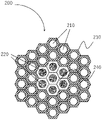
FIG. 1 is a diagram schematically showing a cross section of the Nb 3 Sn superconducting wire precursor of the present invention.
本発明の前駆体100は、少なくともニオブ(Nb)を含有するNb基からなる1以上のNb芯110と、少なくともスズ(Sn)および亜鉛(Zn)を含有するSn基からなる1以上のSn芯120と、銅(Cu)を主成分とし、チタン(Ti)をさらに含有する1以上の第1のCu母材130と、銅(Cu)を主成分とする1以上の第2のCu母材140とを備える。第1のCu母材130はNb芯110を埋設し、第2のCu母材140はSn芯120を埋設する。
The
本発明の前駆体100は、Tiが、Nb芯ではなく、少なくとも第1のCu母材に添加されており、Znが、Cu母材ではなく、Sn芯に添加されている点が、特許文献1~3および非特許文献1と異なる。本願発明者は、Tiを第1のCu母材130に、ZnをSn芯120にそれぞれ添加することにより、熱処理時にTiリッチ層の形成が抑制されることを見出した。その結果、SnおよびTiが第1のCu母材130および第2のCu母材140中を容易に拡散し、Nb3Sn相の生成を促進できる。In the
各構成要素について詳細に説明する。
Nb芯110を構成するNb基は、Nb金属単体であってもよいが、Nb以外にチタン(Ti)、タンタル(Ta)、ハフニウム(Hf)およびジルコニウム(Zr)からなる群から選択される少なくとも1種の元素をさらに含有してもよい。これらの元素は、Nb3Snの臨界磁場を向上させることができる。また、Nb3Sn結晶粒を微細化できるので、臨界電流密度の改善も期待できる。Each component will be described in detail.
The Nb group constituting the
これらの元素の添加量は、好ましくは、0at%より多く5at%以下の範囲である。5at%を超えると臨界磁場の向上の効果が小さくなり得る。これらの元素の添加量は、より好ましくは、0.5at%以上2at%以下の範囲である。この範囲であれば、臨界磁場が向上し、Nb3Sn結晶粒を微細化し得る。The amount of these elements added is preferably in the range of more than 0 atomic % and 5 atomic % or less. If it exceeds 5 at %, the effect of improving the critical magnetic field may become small. The amount of these elements to be added is more preferably in the range of 0.5 at % or more and 2 at % or less. Within this range, the critical magnetic field is improved and the Nb 3 Sn crystal grains can be refined.
Sn芯120を構成するSn基は、少なくともSnとZnを含有していればよく、SnとZnとの合金であれば特に制限はないが、好ましくは、Sn基中のZnの含有量は、1wt%以上40wt%以下の範囲である。1wt%未満になると、Sn芯120硬度の改善が小さくなり得、40wt%を超えると、Sn基の組織が粗大化するため、前駆体100の加工性が低下し得る。より好ましくは、Sn基中のZnの含有量は、10wt%以上25wt%以下の範囲である。この範囲であれば、前駆体全体の硬度が向上し、加工性に優れる。なおさらに好ましくは、Sn基中のZnの含有量は、15wt%以上25wt%以下の範囲である。なお、本願明細書では、「wt%」を使用するが、「mass%」を用いてもよい。つまり、本願明細書では、そこに記載の「wt%」を「mass%」で置き換えてもよい。
The Sn group that constitutes the
Sn基は、少なくともSnとZnを含有していればよく、SnとZnとの合金であれば特に制限はないが、好ましくは、マグネシウム(Mg)、ゲルマニウム(Ge)、ガリウム(Ga)、アルミニウム(Al)およびインジウム(In)からなる群から選択される少なくとも1種の元素をさらに含有する。これらの元素の含有は、Sn基の組織を微細化し、硬度を改善できる。 The Sn group may contain at least Sn and Zn, and is not particularly limited as long as it is an alloy of Sn and Zn, but preferably magnesium (Mg), germanium (Ge), gallium (Ga), aluminum It further contains at least one element selected from the group consisting of (Al) and indium (In). The inclusion of these elements can refine the Sn-based structure and improve the hardness.
特に、Mgは、Nb3Sn結晶粒の微細化に有利であり、Geは、Nb3Snの臨界磁場の向上およびNb3Sn結晶粒の微細化に有利であり、Gaは、Nb3Snの臨界温度および臨界磁場の向上に有利であり、Alは、Nb3Snの臨界温度の向上に有利であり、Inは、Nb3Sn相の生成促進、Nb3Snの臨界磁場の向上およびNb3Sn結晶粒の微細化に有利である。これらの元素を1つまたは複数適宜選択して用いてよい。In particular, Mg is advantageous for refining Nb 3 Sn crystal grains, Ge is advantageous for improving the critical magnetic field of Nb 3 Sn and refining Nb 3 Sn crystal grains, and Ga is advantageous for refining Nb 3 Sn. Al is advantageous for improving the critical temperature and critical magnetic field of Nb 3 Sn, and In promotes the formation of the Nb 3 Sn phase, improves the critical magnetic field of Nb 3 Sn, and improves the critical magnetic field of Nb 3 Sn. It is advantageous for refining Sn crystal grains. One or a plurality of these elements may be appropriately selected and used.
これらの元素の含有量は、好ましくは、1wt%以上40wt%以下の範囲である。この範囲であれば、Sn基の組織を微細化し得る。さらに好ましくは、これらの元素の含有量は、1wt%以上10wt%以下の範囲であり、なお好ましくは、1wt%以上5wt%以下の範囲である。複数の元素を含有する場合には、これらの合計が上記範囲であればよい。 The content of these elements is preferably in the range of 1 wt % or more and 40 wt % or less. Within this range, the structure of the Sn group can be refined. More preferably, the content of these elements is in the range of 1 wt % or more and 10 wt % or less, and still more preferably in the range of 1 wt % or more and 5 wt % or less. When a plurality of elements are contained, the total of these elements should be within the above range.
第1のCu母材130は、Cuを主成分としてTiを含有していれば特に制限はない。ここでCuの主成分とする量(すなわち、本願明細書において、第1のCu母材における「Cuを主成分」と称する場合のCu含有量)は、CuとTiとの合金となる量であるが、本願明細書ではCuを80wt%以上とする。
The first
第1のCu母材130中のTiの含有量は、好ましくは、0wt%より多く5wt%以下の範囲である。5wt%を超えると、第1のCu母材130の加工硬化が大きくなり得、前駆体100の加工性が低下する虞がある。より好ましくは、Tiの含有量は、0.5wt%以上3wt%以下の範囲である。この範囲であれば、第1のCu母材130の加工性に優れ、熱処理時にTiリッチ層の形成を抑制できる。より好ましくは、Tiの含有量は、0.5wt%以上2wt%以下の範囲である。なおさらに好ましくは、Tiの含有量は、0.5wt%以上1.5wt%以下の範囲である。
The content of Ti in the first
第2のCu母材140は、Cuを主成分としており、Cu単体であってもよいし、さらにTiを含有してもよい。この場合も、Tiを含有する場合のTiの含有量は、第1のCu母材130と同様に、0wt%より多く5wt%以下の範囲、好ましくは、0.5wt%以上3wt%以下の範囲、より好ましくは、0.5wt%以上2wt%以下の範囲、なおさらに好ましくは0.5wt%以上1.5wt%以下の範囲である。ここで、Cuの主成分とする量(すなわち、本願明細書において、第2のCu母材における「Cuを主成分」と称する場合のCu含有量)も、第1のCu母材の場合と同様、80wt%以上とする。
The second
第2のCu母材140がTiを含有する場合、第1のCu母材130と同一であってもよい。これにより、前駆体の製造方法によっては、製造効率が向上し得る。
When the second
なお、Nb基、Sn基、第1のCu母材および第2のCu母材は、上述した金属元素以外に不可避不純物を含有し得る。 In addition, the Nb group, the Sn group, the first Cu base material, and the second Cu base material may contain unavoidable impurities other than the metal elements described above.
Sn芯120に対するNb芯110の体積比は、好ましくは、1以上3以下の範囲である。1未満の場合、熱処理後の超伝導線材断面積内のNb3Snの生成量が少なくなり得、高い特性が得られにくい可能性がある。一方、3を超えると、未反応のNb芯110が多くなり、超伝導線材の臨界電流密度(Jc)を低下させる虞がある。The volume ratio of the
なお、Sn芯120に対するNb芯110の体積比は、例えば、図1または後述する図2に示す前駆体100、200の場合には、次のようにして算出される。Sn芯120(図2に示す前駆体200では、Sn芯220を指す)がa本、Nb芯110(図2に示す前駆体200では、Nb芯210を指す)がb本、Sn芯120の1本に対するNb芯110の面積比率をxとし、体積比vは、v=a×x/bで算出される。
The volume ratio of the
前駆体100は、伸線加工された伸線加工品であってもよい。伸線加工品とは、伸線加工により、前駆体100を半径方向に縮径した状態の成形品を意図する。なお、伸線加工前後において前駆体100は、縮径以外の配置構造の変化は実質ない。
The
前駆体100が伸線加工品である場合、Sn芯120を構成するSn基中のZnが微細化され、均一に分散されている。これにより、Sn芯120の硬度が高まり、前駆体全体の硬さのバランスが改善され、伸線加工性を向上できる。Sn芯120を構成するSn基の組織中のZnは、伸線加工前は、デンドライト状であるが、伸線加工後は、デンドライト状がなくなり、全体に均一な組織となる。このような状態をZnが均一に分散されているという。Sn基の組織は、光学顕微鏡観察によって確認できる。
When the
図1では、第1のCu母材130および第2のCu母材140は、複数の穴(それぞれ30個および7個)を有する管状の形状を有しており、第1のCu母材130に埋設されたフィラメント状のNb基からなる30本のNb芯110、および、第2のCu母材140に埋設されたフィラメント状のSn基からなる7本のSn芯120を備える前駆体100を示すが、穴の数、Nb芯110およびSn芯120の数はこれに限らない。第1のCu母材130および第2のCu母材140の穴の数は、それぞれ、複数であってもよいし、1つであってもよい。
In FIG. 1, the
また、Nb芯110は、フィラメント状以外にも粉末状あるいはチップ状のNb基からなってもよく、Sn芯は、フィラメント状以外にも粉末状あるいはチップ状のSn基からなってもよい。本願明細書において、フィラメント状は線状の形態を有するものを意図し、粉末状とは粉や粒などの形態を有するものを意図し、チップ状とは、粉末状よりも大きな小片であり、例えば、金属板などを裁断して得られるものを意図する。
In addition, the
図1では、Nb芯110は、Sn芯120の周りに配置されるように示すが、これに限らない。Nb芯110およびSn芯120の配置はあくまでも例示であって、当業者であれば、適宜変更できることに留意されたい。
In FIG. 1, the
図2は、別の本発明のNb3Sn超伝導線材用前駆体の断面を模式的に示す図である。FIG. 2 is a diagram schematically showing a cross section of another Nb 3 Sn superconducting wire precursor of the present invention.
図2の前駆体200は、少なくともNbを含有するNb基からなる1以上のNb芯210と、少なくともSnおよびZnを含有するSn基からなる1以上のSn芯220と、Nb芯210が埋設されるCuを主成分とし、Tiをさらに含有する1以上の第1のCu母材230と、Sn芯220が埋設されるCuを主成分とする1以上の第2のCu母材240とを備える。Nb芯210、Sn芯220、第1のCu母材230および第2のCu母材240は、それぞれ、図1を参照して説明した、Nb芯110、Sn芯120、第1のCu母材130および第2のCu母材140と同様であるため、説明を省略する。
In the
図2では、第1のCu母材230および第2のCu母材240のそれぞれが複数の管である点が、図1とは異なるが、それ以外は同様である。
FIG. 2 differs from FIG. 1 in that each of the first
図2では、それぞれが第1のCu母材230に埋設されたフィラメント状のNb基からなる30本のNb芯210、および、それぞれが第2のCu母材240に埋設されたフィラメント状のSn基からなる7本Sn芯220を備える前駆体200を示すが、Nb芯210およびSn芯220の数はこれに限らない。また、フィラメント状のNb基およびSn基に代えて、チップ状あるいは粉末状のNb基およびSn基を用いてもよいことはいうまでもない。
In FIG. 2, 30
図2では、Nb芯210を単芯で示すが、Nb芯210は、Nb芯と第1のCu母材とが複合化した多芯であってもよい。このような改変は当業者であれば、容易に想到する。同様に、Sn芯220も、Sn芯と第2のCu母材とが複合化した多芯であってもよい。
In FIG. 2, the
図2の前駆体200も、前駆体100と同様に、伸線加工された伸線加工品であってもよい。
Like the
前駆体200は、Nb、Ta等のバリア層を有するCu製の管(図示せず)を外側に有していてもよい。
The
図3は、さらに別の本発明のNb3Sn超伝導線材用前駆体の断面を模式的に示す図である。FIG. 3 is a diagram schematically showing a cross section of still another Nb 3 Sn superconducting wire precursor of the present invention.
図3(A)の前駆体300は、少なくともNbを含有するNb基からなる1以上のNb芯310と、少なくともSnおよびZnを含有するSn基からなる1以上のSn芯320と、Nb芯310が埋設されるCuを主成分とし、Tiをさらに含有する1以上の第1のCu母材330と、Sn芯320が埋設されるCuを主成分とする1以上の第2のCu母材340とを備える。Nb芯310、Sn芯320、第1のCu母材330および第2のCu母材340は、それぞれ、図1を参照して説明した、Nb芯110、Sn芯120、第1のCu母材130および第2のCu母材140と同様であるため、説明を省略する。
The
図3(A)では、Nb基(Nb芯310に相当)、Sn基(Sn芯320に相当)、第1のCu母材330および第2のCu母材340は、シート状の形状を有し、積層され、ジェリーロールをなしている点が、図1とは異なる。なお、積層に際して、Nb芯310とSn芯320とは、第1のCu母材330または第2のCu母材340を介さず直接積層することはない。
In FIG. 3A, the Nb group (corresponding to the Nb core 310), the Sn group (corresponding to the Sn core 320), the first
図3のジェリーロールにおいては、Nb芯310、Sn芯320、第1のCu母材330および第2のCu母材340の数をシート数とみなしてよい。
In the jelly roll of FIG. 3, the number of
図3(A)では、外側から、第1のCu母材330、Nb芯310、第1のCu母材330、第2のCu母材340、Sn芯320、第2のCu母材340、第1のCu母材330、Nb芯310、・・・を繰り返すように積層されているが、積層の順番は、Nb芯310にSn芯320中のSnが拡散する限り、これに限らない。
In FIG. 3A, from the outside, the first
好ましくは、図3(B)の前駆体301に示されるように、第2のCu母材340は、Tiを含有しており、第1のCu母材330と同一である。これにより、Nb芯310およびSn芯320は、第1のCu母材330を介して積層されることになる。この場合、第1のCu母材330、Nb芯310、第1のCu母材330、Sn芯320、第1のCu母材330、Nb芯310、・・・を繰り返すように積層すればよい。このような構造とすることにより、製造工程が煩雑となるのを避け、歩留まりよく製造できる。
Preferably, the
図3の前駆体300、301の場合、組み込むSn芯320に対するNb芯310の体積比は、使用するそれぞれのシートの厚み、幅、長さから算出できる。
For
図3の前駆体300、301も、前駆体100と同様に、伸線加工された伸線加工品であってもよい。
Like the
図3では、前駆体300、301の最外層が第1のCu母材330となっているが、例えば、前駆体300、301が、Nb、Ta等のバリア層を有するCu製の管(図示せず)を外側に有する場合には、最外層はNb芯310やSn芯320であってもよい。
In FIG. 3, the outermost layer of the
次に、本発明のNb3Sn超伝導線材用前駆体は、概略以下のようにして製造される。少なくともNbを含有するNb基と、少なくともSnおよびZnを含有するSn基と、Cuを主成分とし、Tiをさらに含有する第1のCu母材と、Cuを主成分とする第2のCu母材とに、ロッド・イン・チューブ(RIT)法、ジェリーロール法およびパウダー・イン・ロール(PIT)法からなる群から選択される手法を適用することによって、本発明の前駆体は製造される。ここで、Nb基、Sn基、第1のCu母材および第2のCu母材は、図1を参照して説明したとおりであるため、説明を省略する。Next, the Nb 3 Sn superconducting wire precursor of the present invention is produced roughly as follows. A Nb group containing at least Nb, a Sn group containing at least Sn and Zn, a first Cu base material containing Cu as a main component and further containing Ti, and a second Cu base material containing Cu as a main component The precursor of the present invention is produced by applying a method selected from the group consisting of rod-in-tube (RIT) method, jelly-roll method and powder-in-roll (PIT) method to the material. . Here, since the Nb group, the Sn group, the first Cu base material and the second Cu base material are as described with reference to FIG. 1, the description thereof is omitted.
このようにして得られた前駆体に伸線加工を施してもよい。これにより、Sn基中のZnが均一に分散されるので、Sn芯の硬度が高まり、前駆体の加工性を向上できる。伸線加工は、例えば、ダイスを用いた公知の加工手法によって行われる。 The precursor thus obtained may be subjected to wire drawing. As a result, Zn in the Sn group is uniformly dispersed, so that the hardness of the Sn core increases and the workability of the precursor can be improved. Wire drawing is performed, for example, by a known processing method using a die.
図1~図3の前駆体の製造方法について詳細に説明する。
図4は、図1に示す前駆体を製造する製造工程を示すフローチャートである。A method for manufacturing the precursors shown in FIGS. 1 to 3 will be described in detail.
FIG. 4 is a flowchart showing manufacturing steps for manufacturing the precursor shown in FIG.
ステップS410:棒状の第1のCu母材に1以上の穴を形成、それぞれの穴にフィラメント状のNb基を挿入し、Nb芯を形成する。すなわち、Cuを主成分とし、Tiをさらに含有する第1のCu母材に穴を形成し、少なくともNbを含有するNb基を挿入し、Nb芯を形成する。
ステップS420:棒状の第2のCu母材に1以上の穴を形成し、それぞれのフィラメント状のSn基を挿入し、Sn芯を形成する。すなわち、Cuを主成分とする第2のCu母材に穴を形成し、少なくともSnおよびZnを含有するSn基を挿入し、Sn芯を形成する。ステップS410およびステップS420を用いた手法は、ロッド・イン・チューブ(RIT)法と呼ばれる。
ステップS430:ステップS410によって得られたNb芯が形成(挿入)された第1のCu母材、および、ステップS420によって得られたSn芯が形成(挿入)された第2のCu母材を束ねる。
ステップS440:伸線加工する。Step S410: Form one or more holes in the rod-like first Cu base material, and insert filament-like Nb groups into each hole to form an Nb core. That is, holes are formed in a first Cu base material containing Cu as a main component and further containing Ti, and Nb groups containing at least Nb are inserted to form Nb cores.
Step S420: Form one or more holes in the rod-like second Cu base material to insert respective filament-like Sn groups to form Sn cores. That is, holes are formed in the second Cu base material containing Cu as a main component, Sn groups containing at least Sn and Zn are inserted, and Sn cores are formed. A method using steps S410 and S420 is called a rod-in-tube (RIT) method.
Step S430: Bundle the first Cu base material with Nb core formed (inserted) obtained in step S410 and the second Cu base material with Sn core formed (inserted) obtained in step S420. .
Step S440: Wire drawing.
ステップS430により本発明の前駆体100(図1)が得られるが、必要に応じて、伸線加工(ステップS440)を行ってもよい。 Precursor 100 (FIG. 1) of the present invention is obtained by step S430, and wire drawing (step S440) may be performed as necessary.
ステップS410において、得られたNb芯が形成された第1のCu母材を中間焼鈍してもよい。これにより、Nbおよび第1のCu母材の加工歪みを除去できる。中間焼鈍は、好ましくは、真空中または不活性ガス雰囲気中、400℃以上600℃以下の温度範囲で行われる。真空は、例えば、1×10⁻³Pa以上の真空度であり、不活性ガス雰囲気は、窒素(N2)、アルゴン(Ar)等の希ガスであり得る。真空であればよいので、上限は、大気圧以下(例えば、1×10⁵Pa以下)であればよい。In step S410, the obtained first Cu base material having the Nb core formed thereon may be intermediate annealed. As a result, processing distortions in Nb and the first Cu base material can be removed. Intermediate annealing is preferably performed in a vacuum or inert gas atmosphere at a temperature range of 400° C. or higher and 600° C. or lower. The vacuum is, for example, a degree of vacuum of 1×10 −3 Pa or higher, and the inert gas atmosphere can be nitrogen (N 2 ), rare gas such as argon (Ar). Since vacuum is sufficient, the upper limit may be atmospheric pressure or less (for example, 1×10 5 Pa or less).
また、ステップS410およびステップS420は、ステップS410、ついで、ステップS420の順に行ってもよいし、ステップS420、次いで、ステップS410の順に行ってもよい。 Steps S410 and S420 may be performed in the order of step S410 and then step S420, or step S420 and then step S410.
また、第2のCu母材が、第1のCu母材と同じ場合には、ステップS410において、Nb芯用の穴に加えて、Sn芯用の穴を形成してもよい。 Further, when the second Cu base material is the same as the first Cu base material, in step S410, holes for Sn cores may be formed in addition to holes for Nb cores.
例えば、第2のCu母材が第1のCu母材と同じ場合、外形30mmを有する第1のCu母材に、内径2mmを有する穴を放射状に42個形成し、そのうちの、外側の30個の穴にNb芯を形成し、内側の12個の穴にSn芯を形成すれば前駆体100が得られる。これを外形1mmまで伸線加工してもよい。なお、外形、内径、穴の数等はあくまでも例示であって、Nb芯/Sn芯の体積比によって適宜変更されてよい。
For example, when the second Cu base material is the same as the first Cu base material, 42 holes having an inner diameter of 2 mm are radially formed in the first Cu base material having an outer diameter of 30 mm.
図5は、図2に示す前駆体を製造する製造工程を示すフローチャートである。 FIG. 5 is a flow chart showing manufacturing steps for manufacturing the precursor shown in FIG.
ステップS510:1以上の管状の第1のCu母材のそれぞれにNb基を挿入し、Nb芯を形成する。Nb基は、フィラメント状であってもよいし、粉末状であってもよいし、チップ状であってもよい。すなわち、Cuを主成分とし、Tiをさらに含有する管状の第1のCu母材に、少なくともNbを含有するNb基を挿入し、Nb芯を形成する。
ステップS520:1以上の管状の第2のCu母材のそれぞれにSn基を挿入し、Sn芯を形成する。Sn基は、フィラメント状であってもよいし、粉末状であってもよいし、チップ状であってもよい。すなわち、Cuを主成分とする管状の第2のCu母材に、少なくともSnおよびZnを含有するSn基を挿入し、Sn芯を形成する。ステップS510およびステップS520を用いたこのような手法は、管に挿入される材料の様態によって、ロッド・イン・チューブ(RIT)法またはパウダー・イン・チューブ(PIT)法と呼ばれる。
ステップS530:ステップS510で得られた管状部材とステップS520で得られた管状部材とを束ねる。
ステップS530:伸線加工する。Step S510: Insert Nb groups into each of the one or more tubular first Cu base materials to form Nb cores. The Nb group may be filament-like, powder-like, or chip-like. That is, Nb groups containing at least Nb are inserted into a tubular first Cu base material containing Cu as a main component and further containing Ti to form an Nb core.
Step S520: Insert Sn groups into each of the one or more tubular second Cu base materials to form Sn cores. The Sn group may be filamentary, powdery, or chip-shaped. That is, Sn groups containing at least Sn and Zn are inserted into a tubular second Cu base material containing Cu as a main component to form an Sn core. Such a technique using steps S510 and S520 is called a rod-in-tube (RIT) technique or a powder-in-tube (PIT) technique, depending on the manner in which the material is inserted into the tube.
Step S530: Bundling the tubular member obtained in step S510 and the tubular member obtained in step S520.
Step S530: Wire drawing.
ここでも、ステップS510によって得られた管状部材(Nb芯が挿入された管状の第1のCu母材)、および、ステップS520によって得られた管状部材(Sn芯が挿入された管状の第2のCu母材)を束ねて本発明の前駆体200(図2)が得られるが、必要に応じて、伸線加工(ステップS530)を行ってもよい。 Here, too, the tubular member obtained in step S510 (tubular first Cu base material with Nb core inserted) and the tubular member obtained in step S520 (tubular second tubular member with Sn core inserted) Cu base material) are bundled to obtain the precursor 200 (FIG. 2) of the present invention, but if necessary, wire drawing (step S530) may be performed.
ステップS510において、得られた管状部材を中間焼鈍してもよい。中間焼鈍の条件は、ステップS410と同様である。 At step S510, the resulting tubular member may be intermediate annealed. The conditions for intermediate annealing are the same as in step S410.
ステップS510において、得られた管状部材を伸線加工し、六角形状に加工し、複数の六角形状の管状部材を別の管状の第1のCu母材に挿入し、さらに伸線加工、六角形状に加工してもよい。これにより、多芯のNb芯となる。 In step S510, the obtained tubular member is wire-drawn, processed into a hexagonal shape, a plurality of hexagonal tubular members are inserted into another tubular first Cu base material, and further wire-drawn to form a hexagonal shape. can be processed into As a result, a multi-core Nb core is obtained.
ステップS520において、得られた管状部材を伸線加工し、六角形状に加工してもよい。これにより、ステップS510およびステップS520でえられた管状部材を隙間なく束ねることができる。 At step S520, the resulting tubular member may be drawn into a hexagonal shape. As a result, the tubular members obtained in steps S510 and S520 can be bundled without gaps.
ステップS530において、管状の内側にNb、Ta等のバリア層を有するCu製の管に上記管状部材を挿入し、束ねてもよい。 In step S530, the tubular member may be inserted into a Cu tube having a barrier layer such as Nb, Ta, etc. inside the tube and bundled.
図6は、図3に示す前駆体を製造する製造工程を示すフローチャートである。 FIG. 6 is a flowchart showing manufacturing steps for manufacturing the precursor shown in FIG.
ステップS610:シート状のNb基からなるNb芯と、シート状のSn基からなるSn芯と、シート状の第1のCu母材と、シート状の第2のCu母材とを積層し、ジェリーロール状に巻く。すなわち、少なくともNbを含有するNb基からなるシート状のNb芯と、少なくともSnおよびZnを含有するSn基からなるシート状のSn芯と、Cuを主成分とし、Tiをさらに含有するシート状の第1のCu母材と、Cuを主成分とするシート状の第2のCu母材とを積層し、ジェリーロール状に巻く。このような手法は、ジェリーロール法と呼ばれる。
ステップS620:伸線加工する。Step S610: A sheet-like Nb-based Nb core, a sheet-like Sn-based Sn core, a sheet-like first Cu base material, and a sheet-like second Cu base material are laminated, Roll into a jelly roll. That is, a sheet-shaped Nb core made of an Nb group containing at least Nb, a sheet-shaped Sn core made of an Sn group containing at least Sn and Zn, and a sheet-shaped Sn core containing Cu as a main component and further containing Ti A first Cu base material and a sheet-like second Cu base material containing Cu as a main component are laminated and wound into a jelly roll. Such a method is called a jelly roll method.
Step S620: Wire drawing.
ここでも、ステップS610によってジェリーロール状の前駆体300(図3(A))が得られるが、必要に応じて、伸線加工(ステップS620)を行ってもよい。 Again, the jelly roll-shaped precursor 300 (FIG. 3A) is obtained in step S610, but wire drawing (step S620) may be performed as necessary.
ステップS610において、Nb芯が第1のCu母材に埋設され、Sn芯が第2のCu母材に埋設されるよう、シート状のNb基は、一対のシート状の第1のCu母材間に位置し、シート状のSn基は、一対のシート状の第2のCu母材間に位置するよう、各シートを積層することが好ましい。 In step S610, the sheet-like Nb base is embedded in a pair of sheet-like first Cu base materials such that the Nb core is embedded in the first Cu base material and the Sn core is embedded in the second Cu base material. Preferably, the sheets are laminated such that the sheet-like Sn groups are positioned between a pair of sheet-like second Cu base materials.
ステップS610において、さらに好ましくは、第2のCu母材は、第1のCu母材と同一であり、シート状のNb基からなるNb芯と、シート状のSn基からなるSn芯と、シート状の第1のCu母材とを積層し、ジェリーロール状に巻けばよい。このようにしてジェリーロール状の前駆体301(図3(B))が得られる。この場合、例えば、シート状の第1のCu母材、シート状のNb基、シート状の第1のCu母材、シート状のSn基の順に積層できるので、製造工程が簡略化され、歩留まりよく前駆体を製造できる。 In step S610, more preferably, the second Cu base material is the same as the first Cu base material, and includes a sheet-like Nb-based Nb core, a sheet-like Sn-based Sn core, and a sheet , and the first Cu base material having a shape, and wound in a jelly roll shape. Thus, a jelly roll-shaped precursor 301 (FIG. 3(B)) is obtained. In this case, for example, since the sheet-like first Cu base material, the sheet-like Nb base, the sheet-like first Cu base material, and the sheet-like Sn base can be laminated in this order, the manufacturing process is simplified and the yield is improved. Good precursors can be made.
例えば、第2のCu母材が第1のCu母材と同じ場合、厚さ100μmのシート状のNb芯と、厚さ50μmのシート状のSn基と、厚さ30μmのシート状の第1のCu母材とを用い、第1のCu母材、Nb基、第1のCu母材およびSn基の順に30回繰り返し積層し、ジェリーロール状に巻けば前駆体が得られる。これを外形1mmまで伸線加工してもよい。なお、シートの厚さ、積層数等はあくまでも例示であって、Nb芯/Sn芯の体積比によって適宜変更されてよい。 For example, when the second Cu base material is the same as the first Cu base material, a sheet-like Nb core with a thickness of 100 μm, a sheet-like Sn base with a thickness of 50 μm, and a sheet-like first sheet with a thickness of 30 μm The first Cu base material, the Nb base, the first Cu base material and the Sn base are laminated in this order 30 times, and wound into a jelly roll to obtain a precursor. This may be wire-drawn to an outer diameter of 1 mm. Note that the thickness of the sheet, the number of layers, etc. are merely examples, and may be appropriately changed depending on the volume ratio of the Nb core/Sn core.
(実施の形態2)
実施の形態2は、実施の形態1で説明した前駆体を用いて、内部スズ法によってNb3Sn超伝導線材の製造方法について説明する。(Embodiment 2)
Embodiment 2 describes a method of manufacturing a Nb 3 Sn superconducting wire by the internal tin method using the precursor described in
実施の形態1で説明したNb3Sn超伝導線材用の前駆体を熱処理することによって、前駆体内でSnおよびTiが第1および第2のCu母材中に拡散し、Nb基がNb3Sn相となり、Nb3Sn超伝導線材が得られる。以下、詳細に説明する。By heat-treating the precursor for the Nb 3 Sn superconducting wire described in
図7は、本発明の前駆体を用いたNb3Sn超伝導線材を製造する製造工程を示すフローチャートである。FIG. 7 is a flow chart showing manufacturing steps for manufacturing a Nb 3 Sn superconducting wire using the precursor of the present invention.
ステップS710:Nb3Sn超伝導線材用の前駆体を、真空または不活性ガス雰囲気中、200℃以上600℃未満の温度範囲で予備加熱する。
ステップS720:Nb3Sn超伝導線材用の前駆体を、真空または不活性ガス雰囲気中、600℃以上800℃以下の温度範囲で加熱する。Step S710: A precursor for the Nb3Sn superconducting wire is preheated in a vacuum or inert gas atmosphere at a temperature range of 200°C or higher and lower than 600°C.
Step S720: The precursor for the Nb3Sn superconducting wire is heated in a temperature range of 600°C or higher and 800°C or lower in a vacuum or inert gas atmosphere.
ステップS710の予備加熱は、必須ではないが、上記温度範囲で加熱することにより、Tiリッチ層が形成されることなく、第1のCu母材および第2のCu母材中のCuと、Znと、Snとの相互拡散を促進できるため、線材断面内において、均質にNb3Sn相を生成できる。予備加熱は、好ましくは、400℃以上600℃未満の温度範囲である。Preheating in step S710 is not essential, but by heating in the above temperature range, Cu and Zn in the first Cu base material and the second Cu base material do not form a Ti-rich layer. and Sn can promote interdiffusion, so that the Nb 3 Sn phase can be homogeneously generated in the cross section of the wire. The preheating is preferably performed within a temperature range of 400°C or higher and lower than 600°C.
ステップS710において、予備加熱する雰囲気は、真空または不活性ガス雰囲気であればよく、真空は、例えば、1×10⁻³Pa以上真空度であり、不活性ガス雰囲気は、窒素(N2)、アルゴン(Ar)等の希ガスであり得る。真空であればよいので、上限は、大気圧以下(例えば、1×10⁵Pa以下)であればよい。 In step S710 , the atmosphere to be preheated may be a vacuum or an inert gas atmosphere. It can be a noble gas such as argon (Ar). Since vacuum is sufficient, the upper limit may be atmospheric pressure or less (for example, 1×10 5 Pa or less).
ステップS710において、予備加熱する時間は、特に制限はないが、例示的には、400℃以上600℃未満の温度範囲で10時間以上200時間以下の範囲である。 In step S710, the preheating time is not particularly limited, but is illustratively in the range of 10 hours or more and 200 hours or less at a temperature range of 400° C. or more and less than 600° C.
ステップS720において、熱処理を上記温度範囲で行えば、ステップS710の予備加熱をしない場合であっても、Tiリッチ層が形成されず、第1のCu母材および第2のCu母材中のCuと、Znと、Snとの相互拡散を促進し、Nb3Sn相の生成を促進できる。また、結晶粒の粗大化を抑制した、高い臨界電流密度を有するNb3Sn超伝導線材を提供できる。なお、Nb3Sn相の生成は、前駆体の端部を電子顕微鏡等によって観察することによって簡易的に判断できる。例えば、端部の断面において、Nb芯についてエネルギー分散型X線分析(EDX)等によってNbとSnの組成分析を行い、Nb/Sn比率が概ね3程度であれば、Nb3Sn相が生成したと判断してよい。If the heat treatment is performed in the above temperature range in step S720, a Ti-rich layer is not formed even if the preheating in step S710 is not performed, and the Cu in the first Cu base material and the second Cu base material , promotes interdiffusion of Zn and Sn, and promotes formation of the Nb 3 Sn phase. In addition, it is possible to provide a Nb 3 Sn superconducting wire having a high critical current density in which coarsening of crystal grains is suppressed. The generation of the Nb 3 Sn phase can be easily determined by observing the edge of the precursor with an electron microscope or the like. For example, in the cross section of the edge, composition analysis of Nb and Sn was performed on the Nb core by energy dispersive X-ray analysis (EDX) or the like, and if the Nb/Sn ratio was approximately 3, the Nb 3 Sn phase was generated. You can judge.
ステップS720においても、熱処理する雰囲気は、ステップS710と同様に、真空または不活性ガス雰囲気であればよく、真空は、例えば、10-3Pa以上の真空度であり、不活性ガス雰囲気は、窒素(N2)、アルゴン(Ar)等の希ガスであり得る。Also in step S720 , the heat treatment atmosphere may be a vacuum or an inert gas atmosphere, as in step S710. ( N2 ), a noble gas such as argon (Ar).
ステップS720において、熱処理する時間は、特に制限はないが、例示的には、上記温度範囲で50時間以上300時間以下の範囲である。 In step S720, the heat treatment time is not particularly limited, but is illustratively in the range of 50 hours or more and 300 hours or less in the above temperature range.
ステップS720の熱処理を2段階で行ってもよい。詳細には、まず、上記温度範囲の中の第1の温度で加熱し、次いで、第1の温度よりも高い第2の温度で加熱する。このような2段階の熱処理によって、線材断面内において均質なNb3Sn相を有し、高い臨界電流密度を有するNb3Sn超伝導線材が得られる。The heat treatment in step S720 may be performed in two stages. Specifically, first, heating is performed at a first temperature within the above temperature range, and then heating is performed at a second temperature higher than the first temperature. Such a two-stage heat treatment provides a Nb 3 Sn superconducting wire having a homogeneous Nb 3 Sn phase in the cross section of the wire and a high critical current density.
2段階の熱処理において、好ましくは、第1の温度は、600℃以上700℃未満の範囲であり、第2の温度は、700℃以上800℃以下の範囲である。これにより、2段階の熱処理の効果が高まる。また、2段階の熱処理をする場合、2段階の熱処理時間の合計が上述の時間範囲となるようにすればよいが、好ましくは、第1の温度において、50時間以上150時間以下の時間、第2の温度において50時間以上150時間以下の時間加熱する。これにより、2段階の熱処理の効果が高まる。 In the two-stage heat treatment, the first temperature is preferably in the range of 600°C or higher and lower than 700°C, and the second temperature is in the range of 700°C or higher and 800°C or lower. This enhances the effect of the two-stage heat treatment. In the case of two-step heat treatment, the total heat treatment time of the two steps should be within the above-described time range. Heat at the temperature of 2 for 50 hours or more and 150 hours or less. This enhances the effect of the two-stage heat treatment.
次に具体的な実施例を用いて本発明を詳述するが、本発明がこれら実施例に限定されないことに留意されたい。 The present invention will now be described in detail using specific examples, but it should be noted that the present invention is not limited to these examples.
[例1~例11]
例1~例11では、ロッド・イン・チューブ法を採用し、表1に示す構成要素を用いてNb3Sn超伝導線材用前駆体を製造し、前駆体からNb3Sn超伝導線材を製造した。[Examples 1 to 11]
In Examples 1 to 11, a rod-in-tube method was adopted, a precursor for Nb 3 Sn superconducting wire was produced using the components shown in Table 1, and a Nb 3 Sn superconducting wire was produced from the precursor. did.
表1において、「Nb-1wt%Ti」とは、Tiを含有するNb基であり、Tiの含有量が1wt%であり、残部がNbであることを示す。同様に、「Sn-xwt%Zn」とは、Znを含有するSn基であり、Znの含有量がxwt%であり、残部がSnであることを示す。「Sn-20wt%Zn-1wt%Mg」とは、ZnおよびMgを含有するSn基であり、Znの含有量が20wt%であり、Mgの含有量が1wt%であり、残部がSnであることを示す。「Sn-1.6wt%Ti」とは、Tiを含有するSn基であり、Tiの含有量が1.6wt%であり、残部がSnであることを示す。「Cu-ywt%Ti」とは、Tiを含有するCu合金であり、Tiの含有量がywt%であり、残部がCuであることを示す。「Cu-15wt%Zn」とは、Znを含有するCu合金であり、Znの含有量が15wt%であり、残部がCuであることを示す。不可避不純物は、いずれも0.05wt%以下であった。 In Table 1, "Nb-1 wt% Ti" is a Nb group containing Ti, indicating that the content of Ti is 1 wt% and the balance is Nb. Similarly, "Sn-xwt% Zn" is a Sn group containing Zn, indicating that the Zn content is xwt% and the balance is Sn. "Sn-20 wt% Zn-1 wt% Mg" is a Sn group containing Zn and Mg, the Zn content is 20 wt%, the Mg content is 1 wt%, and the balance is Sn indicates that "Sn-1.6 wt% Ti" is a Sn group containing Ti, and indicates that the content of Ti is 1.6 wt% and the balance is Sn. “Cu-ywt%Ti” is a Cu alloy containing Ti, and indicates that the content of Ti is ywt% and the balance is Cu. "Cu-15 wt% Zn" is a Cu alloy containing Zn, and indicates that the content of Zn is 15 wt% and the balance is Cu. Inevitable impurities were all 0.05 wt% or less.

外形/内径が15.0mm/13.5mmの管状の第1のCu母材に直径13.4mmのフィラメント状のNb基を挿入し、Nb芯を形成した(図5のステップS510)。これを直径2.15mmの丸線に伸線加工し、次いで、対辺が1.85mmの六角形状に加工した。これをNb/Cu単芯線と呼ぶ。このNb/Cu単芯線19本を、外形/内径が11.5mm/10.0mmの管状の第1のCu母材に挿入した。次いで、これを直径1.2mmの丸線に伸線加工し、対辺が1.0mmの六角形状に順次加工した。これをNb/Cu多芯線と呼ぶ。 A filament-like Nb group with a diameter of 13.4 mm was inserted into a tubular first Cu base material with an outer diameter/inner diameter of 15.0 mm/13.5 mm to form an Nb core (step S510 in FIG. 5). This was drawn into a round wire with a diameter of 2.15 mm, and then worked into a hexagonal shape with an opposite side of 1.85 mm. This is called an Nb/Cu single core wire. Nineteen of these Nb/Cu single-filamentary wires were inserted into a tubular first Cu base material having an outer diameter/inner diameter of 11.5 mm/10.0 mm. Then, this wire was drawn into a round wire with a diameter of 1.2 mm, and successively processed into a hexagonal shape with an opposite side of 1.0 mm. This is called an Nb/Cu multifilamentary wire.
外形/内径が13.0mm/10.0mmの管状の第2のCu母材に直径9.5mmのフィラメント状のSn基を挿入し、Sn芯を形成した(図5のステップS510)。これを直径1.2mmの丸線に伸線加工し、次いで対辺が1.0mmの六角形状に加工した。これをSn/Cu単芯線と呼ぶ。 A filament-like Sn group with a diameter of 9.5 mm was inserted into a tubular second Cu base material with an outer/inner diameter of 13.0 mm/10.0 mm to form an Sn core (step S510 in FIG. 5). This was drawn into a round wire with a diameter of 1.2 mm, and then worked into a hexagonal shape with an opposite side of 1.0 mm. This is called a Sn/Cu single core wire.
Nb/Cu多芯線とSn/Cu単芯線とを束ねた(図5のステップS530)。詳細には、表2に示す数のNb/Cu多芯線とSn/Cu単芯線とを、内側にNbバリア層が設けられた外形/内径が15.0/8.9mmのCu/Nb管に、真ん中がSn/Cu単芯線、その周りがNb/Cu多芯線となるように挿入し、Nb3Sn超伝導線材用の前駆体を得た。さらに、前駆体を線径0.6mm伸線加工した。表2には、例1~例11の前駆体におけるNb芯/Sn芯の体積比も併せて示す。なお、表2において、「多芯の数」はNb/Cu多芯線の数に、「Nb芯の総数」はNb/Cu単芯線の総数に、「Sn芯の総数」は、Sn/Cu単芯線の総数に相当し、また、「Nb芯/Sn芯の体積比」は、上述のとおりに算出される。伸線加工後の前駆体(伸線加工品)を例1~例11の前駆体と称する。The Nb/Cu multi-filamentary wire and the Sn/Cu single-filamentary wire were bundled (step S530 in FIG. 5). Specifically, the number of Nb/Cu multifilamentary wires and Sn/Cu single-filamentary wires shown in Table 2 were placed in a Cu/Nb tube with an outer/inner diameter of 15.0/8.9 mm and provided with an Nb barrier layer on the inside. , a Sn/Cu single-filamentary wire in the middle and a Nb/Cu multi-filamentary wire around it, to obtain a precursor for a Nb 3 Sn superconducting wire. Further, the precursor was drawn to a wire diameter of 0.6 mm. Table 2 also shows the volume ratio of Nb core/Sn core in the precursors of Examples 1 to 11. In Table 2, "number of multifilaments" is the number of Nb/Cu multifilamentary wires, "total number of Nb filaments" is the total number of Nb/Cu single filamentary wires, and "total number of Sn filaments" is the number of Sn/Cu single filamentary wires. It corresponds to the total number of core wires, and the "Nb core/Sn core volume ratio" is calculated as described above. Precursors (drawn products) after wire drawing are referred to as precursors of Examples 1 to 11.
例1~例11の前駆体の断面を光学顕微鏡(オリンパス製、BX60M)で観察した。結果を図8に示す。また、例1~例11の前駆体の結晶組織を光学顕微鏡で観察し、ビッカース硬度を測定した。結果を図9に示す。 Cross sections of the precursors of Examples 1 to 11 were observed with an optical microscope (Olympus, BX60M). The results are shown in FIG. Also, the crystal structures of the precursors of Examples 1 to 11 were observed with an optical microscope to measure the Vickers hardness. The results are shown in FIG.
さらに、例1~例11の前駆体を、アルゴン(Ar)ガス雰囲気中、550℃で100時間、予備加熱した(図7のステップS710)。予備加熱後の例1~例11の前駆体の断面を、エネルギー分散型X線分光法(EDX、AMTEK製、APOLLO XP)によって組成マッピングを測定した。結果を図10、図11および表3に示す。 Furthermore, the precursors of Examples 1 to 11 were preheated at 550° C. for 100 hours in an argon (Ar) gas atmosphere (step S710 in FIG. 7). Composition mapping of the cross-sections of the precursors of Examples 1 to 11 after preheating was measured by energy dispersive X-ray spectroscopy (EDX, manufactured by AMTEK, APOLLO XP). The results are shown in FIGS. 10, 11 and Table 3.
予備加熱後、前駆体をArガス雰囲気中、Nb3Sn相生成のための熱処理を行った(図7のステップS720)。詳細には、前駆体を650℃で100時間、次いで、715℃で100時間の2段階熱処理をした。熱処理によってNb芯がNb3Sn相になったことを、端部をEDXにより組成分析することによって確認した(Nb/Sn比率は概ね3であった)。熱処理後の前駆体を、例1~例11のNb3Sn超伝導線材と称する。例1~例11のNb3Sn超伝導線材の非銅部臨界電流密度(Jc)を測定した。詳細には、例1~例11のNb3Sn超伝導線材を液体ヘリウムに浸漬し、外部磁場中で通電試験した。結果を図12に示す。After the preheating, the precursor was heat-treated in an Ar gas atmosphere to generate the Nb 3 Sn phase (step S720 in FIG. 7). Specifically, the precursor was subjected to a two-step heat treatment at 650° C. for 100 hours and then at 715° C. for 100 hours. It was confirmed by composition analysis of the end portion by EDX that the Nb core had become the Nb 3 Sn phase by the heat treatment (the Nb/Sn ratio was approximately 3). The precursors after heat treatment are referred to as Nb 3 Sn superconducting wires of Examples 1-11. The non-copper portion critical current densities (Jc) of the Nb 3 Sn superconducting wires of Examples 1 to 11 were measured. Specifically, the Nb 3 Sn superconducting wires of Examples 1 to 11 were immersed in liquid helium and subjected to a power test in an external magnetic field. The results are shown in FIG.
以上の結果をまとめて説明する。
図8は、例1の前駆体の断面の光学顕微鏡像を示す図である。The above results will be summarized and explained.
8 is an optical microscope image of a cross section of the precursor of Example 1. FIG.
図8に示すように、例1の前駆体の断面は、19本のSn/Cu単芯線が中心に位置し、その周囲に、36本のNb/Cu多芯線が配置されていた。例1の前駆体におけるNbバリア内側でのNb芯の占積率は36%であった。例2~例11の前駆体の断面も同様の様態を示し、伸線加工後も設計した配置構造の変化はないことを確認した。 As shown in FIG. 8, the cross-section of the precursor of Example 1 had 19 Sn/Cu single-filamentary wires in the center and 36 Nb/Cu multi-filamentary wires arranged around it. The space factor of the Nb core inside the Nb barrier in the precursor of Example 1 was 36%. The cross-sections of the precursors of Examples 2 to 11 also showed a similar state, confirming that the designed arrangement structure did not change after wire drawing.
図9は、例1の前駆体の伸線加工前後の結晶組織を示す光学顕微鏡像を示す図である。 FIG. 9 is a view showing optical microscope images showing the crystal structure of the precursor of Example 1 before and after wire drawing.
図9(A)は、例1の前駆体の伸線加工前のSn-20wt%Zn芯の結晶組織の様子を示す。図9(B)は、例1の前駆体の伸線加工後のSn-20wt%Zn芯の結晶組織の様子を示す。図9(A)によれば、Znを含有するSn基は溶解鋳造したままであるため、Znがデンドライト状に存在していたが、伸線加工をすることにより、図9(B)に示すように、デンドライト状組織がなくなり、Znが均一分散された。例2~例8、例10および例11の前駆体も同様にデンドライト状組織を有さず、Znが均一に分散していた。 FIG. 9(A) shows the crystal structure of the Sn-20 wt % Zn core before wire drawing of the precursor of Example 1. FIG. FIG. 9B shows the crystal structure of the Sn-20 wt % Zn core after wire drawing of the precursor of Example 1. FIG. According to FIG. 9(A), since the Sn group containing Zn was still melted and cast, Zn was present in the form of dendrites. As shown, the dendritic structure disappeared and Zn was uniformly dispersed. Similarly, the precursors of Examples 2 to 8, 10 and 11 did not have a dendritic structure and Zn was uniformly dispersed.
さらに、例1の前駆体のビッカース硬度は、22Hvであり、例9の前駆体のそれは、12Hvであった。例2~例8、例10および例11の前駆体も20Hvを超えるビッカース硬度を有した。このことから、Sn芯にZnを含有するSn基を用いることにより、前駆体の硬度が向上し、加工性に優れることが示された。 Furthermore, the Vickers hardness of the precursor of Example 1 was 22 Hv and that of the precursor of Example 9 was 12 Hv. The precursors of Examples 2-8, 10 and 11 also had a Vickers hardness greater than 20 Hv. This indicates that the use of a Sn group containing Zn in the Sn core improves the hardness of the precursor and results in excellent workability.
図10は、予備加熱後の例1の前駆体の断面のEDXマッピングを示す図である。
図11は、予備加熱後の例9の前駆体の断面のEDXマッピングを示す図である。FIG. 10 shows an EDX mapping of a cross-section of the precursor of Example 1 after preheating.
FIG. 11 shows an EDX mapping of a cross-section of the precursor of Example 9 after preheating.
図10および図11ではグレースケールで示すが、各図面において明るく示される領域がそれぞれの元素が存在していることを示す。ここで、TiのEDXマッピングに着目すると、図10では全体にTiが分散しているが、図11では、Nb芯の周囲、詳細には、19本のNb芯が集まった周囲であるサブマルチ界面にTiリッチ層が形成されている。表3に示すように、予備加熱後の例2~例8、例10および例11の前駆体も同様に、Tiのリッチ層は確認されず、Tiは一様に分散していた。 10 and 11 are shown in gray scale, the brighter regions in each drawing indicate the presence of the respective element. Here, focusing on the EDX mapping of Ti, Ti is dispersed throughout in FIG. 10, but in FIG. A Ti-rich layer is formed on the . As shown in Table 3, in the precursors of Examples 2 to 8, 10 and 11 after preheating, no Ti-rich layer was observed and Ti was uniformly dispersed.
また、ZnのEDXマッピングに着目すると、図10および図11のいずれにおいても、添加場所(Znは、図10ではSn芯に、図11ではCu母材に添加されている)による差異は見られなかった。 Also, focusing on the EDX mapping of Zn, in both FIGS. 10 and 11, there is no difference depending on the addition location (Zn is added to the Sn core in FIG. 10 and to the Cu base material in FIG. 11). I didn't.
このことから、第1のCu母材がTiを含有することにより、内部スズ法を実施した際にTiリッチ層の形成が抑制され、SnおよびTiがCu母材に容易に拡散し、Nb3Sn相の生成に有利であることが示された。From this, when the first Cu base material contains Ti, the formation of a Ti-rich layer is suppressed when the internal tin method is performed, Sn and Ti easily diffuse into the Cu base material, and Nb 3 It was shown to favor the formation of Sn phases.

図12は、例1および例9のNb3Sn超伝導線材の臨界電流密度の磁場依存性(Jc-B)を示す図である。12 is a diagram showing the magnetic field dependence (Jc-B) of the critical current density of the Nb 3 Sn superconducting wires of Examples 1 and 9. FIG.
図12によれば、測定した磁場の範囲において、例1のNb3Sn超伝導線材(図12では、「new wire」とも称する。)の臨界電流密度は、例9のNb3Sn超伝導線材のそれよりも大きかった。例えば、表4に示すように、4.2K、16Tでは、例1および例9のNb3Sn超伝導線材の臨界電流密度は、それぞれ、797A/mm2および646A/mm2であった。図示しないが、例2~例8、例10および例11のNb3Sn超伝導線材も、同様に例9のNb3Sn超伝導線材よりも大きな臨界電流密度を有した。According to FIG. 12, the critical current density of the Nb 3 Sn superconducting wire of Example 1 (also referred to as “new wire” in FIG. 12) in the range of the magnetic field measured is higher than that of the Nb 3 Sn superconducting wire of Example 9. was larger than that of For example, as shown in Table 4, at 4.2 K and 16 T, the critical current densities of the Nb 3 Sn superconducting wires of Examples 1 and 9 were 797 A/mm 2 and 646 A/mm 2 , respectively. Although not shown, the Nb 3 Sn superconducting wires of Examples 2 to 8, 10 and 11 also had higher critical current densities than the Nb 3 Sn superconducting wire of Example 9.
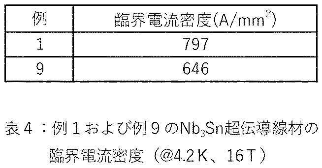
このことから、本発明の前駆体を用いれば、内部スズ法の実施に際して、Tiリッチ層の形成が抑制されるので、SnおよびTiがCu母材へ容易に拡散し、Nb3Sn相の生成が促進される。その結果、線材断面におけるNb3Sn相の均質性が向上し、高い臨界電流密度が得られることが示された。From this, if the precursor of the present invention is used, the formation of a Ti-rich layer is suppressed when the internal tin process is performed, so Sn and Ti easily diffuse into the Cu base material, and the Nb 3 Sn phase is generated. is promoted. As a result, it was shown that the homogeneity of the Nb 3 Sn phase in the cross section of the wire is improved and a high critical current density is obtained.
本発明によれば、均質かつ高い臨界電流密度を有するNb3Sn超伝導線材を提供できるので、(1GHz超)強磁場核磁気共鳴(NMR)装置、核融合炉、高エネルギー粒子加速器、核磁気共鳴画像法(MRI)、超伝導電力貯蔵装置(SMES)等のマグネットに利用され得る。INDUSTRIAL APPLICABILITY According to the present invention, a Nb 3 Sn superconducting wire having a uniform and high critical current density can be provided. It can be used in magnets for resonance imaging (MRI), superconducting power storage devices (SMES), and the like.
100、200、300、301 前駆体
110、210、310 Nb芯
120、220、320 Sn芯
130、230、330 第1のCu母材
140、240、340 第2のCu母材100, 200, 300, 301
Claims (18)
少なくともニオブ(Nb)を含有するNb基からなるNb芯と、
スズ(Sn)および亜鉛(Zn)と、必要に応じて、マグネシウム(Mg)、ゲルマニウム(Ge)、ガリウム(Ga)、アルミニウム(Al)およびインジウム(In)からなる群から選択される少なくとも1種の元素とからなるSn基からなるSn芯と、
銅(Cu)を主成分とし、チタン(Ti)をさらに含有する第1のCu母材と、
Cuを主成分とする第2のCu母材と
を備え、
前記第1のCu母材は前記Nb芯を埋設し、前記第2のCu母材は前記Sn芯を埋設し、
前記Sn基中のZnの含有量は、1wt%以上40wt%以下の範囲であり、
前記第1のCu母材中のTiの含有量は、0.5wt%以上5wt%以下の範囲である、前駆体。 A precursor for a Nb 3 Sn superconducting wire,
a Nb core consisting of a Nb group containing at least niobium (Nb);
Tin (Sn) and zinc (Zn ) and optionally at least one selected from the group consisting of magnesium (Mg), germanium (Ge), gallium (Ga), aluminum (Al) and indium (In) A Sn core consisting of an Sn group consisting of a seed element ,
a first Cu base material containing copper (Cu) as a main component and further containing titanium (Ti);
and a second Cu base material containing Cu as a main component,
The first Cu base material embeds the Nb core, the second Cu base material embeds the Sn core ,
The content of Zn in the Sn group is in the range of 1 wt% or more and 40 wt% or less,
A precursor , wherein the content of Ti in the first Cu base material is in the range of 0.5 wt % or more and 5 wt % or less .
前記Sn基は、粉末状、チップ状およびフィラメント状からなる群から選択される1種の形状を有し、
前記第1のCu母材および前記第2のCu母材は、管状の形状を有する、請求項1~12のいずれかに記載の前駆体。 The Nb group has one shape selected from the group consisting of powdery, chip-like and filamentous,
The Sn group has one shape selected from the group consisting of powdery, chip-like and filamentous,
Precursor according to any one of claims 1 to 12, wherein said first Cu matrix and said second Cu matrix have a tubular shape.
前記Sn基中のZnの含有量は、1wt%以上40wt%以下の範囲であり、
前記第1のCu母材中のTiの含有量は、0.5wt%以上5wt%以下の範囲である、請求項1~14のいずれかに記載のNb3Sn超伝導線材用前駆体の製造方法。 Nb groups containing at least niobium (Nb) , tin (Sn) and zinc (Zn ) and optionally magnesium (Mg), germanium (Ge), gallium (Ga), aluminum (Al) and indium a Sn group consisting of at least one element selected from the group consisting of (In) ; a first Cu base material containing copper (Cu) as a main component and further containing titanium (Ti); applying a method selected from the group consisting of a rod-in-tube method, a jelly-roll method, and a powder-in-tube method to the second Cu base material as the main component ,
The content of Zn in the Sn group is in the range of 1 wt% or more and 40 wt% or less,
The production of the Nb 3 Sn superconducting wire precursor according to any one of claims 1 to 14, wherein the content of Ti in said first Cu base material is in the range of 0.5 wt% or more and 5 wt% or less. Method.
Applications Claiming Priority (3)
| Application Number | Priority Date | Filing Date | Title |
|---|---|---|---|
| JP2019145017 | 2019-08-07 | ||
| JP2019145017 | 2019-08-07 | ||
| PCT/JP2020/008686 WO2021024529A1 (en) | 2019-08-07 | 2020-03-02 | PRECURSOR FOR Nb3Sn SUPERCONDUCTIVE WIRE MATERIAL, PRODUCTION METHOD THEREFOR, AND PRODUCTION METHOD FOR Nb3Sn SUPERCONDUCTIVE WIRE MATERIAL USING SAME |
Publications (2)
| Publication Number | Publication Date |
|---|---|
| JPWO2021024529A1 JPWO2021024529A1 (en) | 2021-12-16 |
| JP7148103B2 true JP7148103B2 (en) | 2022-10-05 |
Family
ID=74502574
Family Applications (1)
| Application Number | Title | Priority Date | Filing Date |
|---|---|---|---|
| JP2021537569A Active JP7148103B2 (en) | 2019-08-07 | 2020-03-02 | Precursor for Nb3Sn superconducting wire, method for producing same, and method for producing Nb3Sn superconducting wire using same |
Country Status (2)
| Country | Link |
|---|---|
| JP (1) | JP7148103B2 (en) |
| WO (1) | WO2021024529A1 (en) |
Families Citing this family (1)
| Publication number | Priority date | Publication date | Assignee | Title |
|---|---|---|---|---|
| WO2022259803A1 (en) | 2021-06-08 | 2022-12-15 | 国立研究開発法人物質・材料研究機構 | Superconducting connection structure of nb3sn superconducting wire rod and nbti wire rod, method for producing same, and nuclear magnetic resonance apparatus using same |
Citations (4)
| Publication number | Priority date | Publication date | Assignee | Title |
|---|---|---|---|---|
| JP2007080616A (en) | 2005-09-13 | 2007-03-29 | Kobe Steel Ltd | MANUFACTURING METHOD OF POWDER METHOD Nb3Sn SUPERCONDUCTIVE WIRE ROD, AND PRECURSOR FOR IT |
| JP2007165152A (en) | 2005-12-14 | 2007-06-28 | Hitachi Cable Ltd | CORE WIRE FOR Nb3Sn SUPERCONDUCTIVE WIRE, Nb3Sn SUPERCONDUCTIVE WIRE, AND METHOD OF MANUFACTURING SAME |
| JP2010262759A (en) | 2009-04-30 | 2010-11-18 | Hitachi Ltd | Nb3sn superconductive wire rod and method for manufacturing the same |
| JP2015185211A (en) | 2014-03-20 | 2015-10-22 | 国立研究開発法人物質・材料研究機構 | METHOD OF PRODUCING Nb3Sn SUPERCONDUCTING WIRE ROD |
Family Cites Families (1)
| Publication number | Priority date | Publication date | Assignee | Title |
|---|---|---|---|---|
| JPS63216212A (en) * | 1987-03-03 | 1988-09-08 | Agency Of Ind Science & Technol | Nb3sn-based superconductive wire and production of it |
-
2020
- 2020-03-02 JP JP2021537569A patent/JP7148103B2/en active Active
- 2020-03-02 WO PCT/JP2020/008686 patent/WO2021024529A1/en active Application Filing
Patent Citations (4)
| Publication number | Priority date | Publication date | Assignee | Title |
|---|---|---|---|---|
| JP2007080616A (en) | 2005-09-13 | 2007-03-29 | Kobe Steel Ltd | MANUFACTURING METHOD OF POWDER METHOD Nb3Sn SUPERCONDUCTIVE WIRE ROD, AND PRECURSOR FOR IT |
| JP2007165152A (en) | 2005-12-14 | 2007-06-28 | Hitachi Cable Ltd | CORE WIRE FOR Nb3Sn SUPERCONDUCTIVE WIRE, Nb3Sn SUPERCONDUCTIVE WIRE, AND METHOD OF MANUFACTURING SAME |
| JP2010262759A (en) | 2009-04-30 | 2010-11-18 | Hitachi Ltd | Nb3sn superconductive wire rod and method for manufacturing the same |
| JP2015185211A (en) | 2014-03-20 | 2015-10-22 | 国立研究開発法人物質・材料研究機構 | METHOD OF PRODUCING Nb3Sn SUPERCONDUCTING WIRE ROD |
Also Published As
| Publication number | Publication date |
|---|---|
| JPWO2021024529A1 (en) | 2021-12-16 |
| WO2021024529A1 (en) | 2021-02-11 |
Similar Documents
| Publication | Publication Date | Title |
|---|---|---|
| US12073958B2 (en) | Diffusion barriers for metallic superconducting wires | |
| US7505800B2 (en) | Superconductive element containing Nb3Sn | |
| JP6719141B2 (en) | Nb3Sn superconducting wire manufacturing method, precursor for Nb3Sn superconducting wire, and Nb3Sn superconducting wire using the same | |
| US7476280B2 (en) | Method for producing a superconductive element | |
| JP6585519B2 (en) | Precursor for producing Nb3Sn superconducting wire, and method for producing Nb3Sn superconducting wire | |
| JP7148103B2 (en) | Precursor for Nb3Sn superconducting wire, method for producing same, and method for producing Nb3Sn superconducting wire using same | |
| JP2007128686A (en) | Nb3Sn SUPERCONDUCTING WIRE MATERIAL MANUFACTURED BY INSIDE DIFFUSION METHOD | |
| EP2333793B1 (en) | Superconductors with improved mechanical strength | |
| JP5805469B2 (en) | Precursor for producing Nb3Sn superconducting wire and Nb3Sn superconducting wire | |
| JP5661582B2 (en) | Precursor for producing Nb3Sn superconducting wire and Nb3Sn superconducting wire | |
| US7887644B2 (en) | Superconductive elements containing copper inclusions, and a composite and a method for their production | |
| US7476281B2 (en) | Method for producing a superconductive element | |
| JP4009167B2 (en) | Powder method Nb (3) Sn superconducting wire | |
| EP1569285B1 (en) | Superconductive element containing Nb3Sn | |
| Morita et al. | Fabrication of New Internal Tin Nb $ _ {3} $ Sn Wire Using Sn-Zn Alloy as Sn Core | |
| JP2007258112A (en) | Method of manufacturing nb base compound superconductive wire | |
| US20220051833A1 (en) | Diffusion barriers for metallic superconducting wires | |
| JP4723345B2 (en) | Method for producing Nb3Sn superconducting wire and precursor therefor | |
| JP2010135215A (en) | PRECURSOR FOR MANUFACTURING Nb3Sn SUPERCONDUCTING WIRE MATERIAL AND Nb3Sn SUPERCONDUCTING WIRE MATERIAL | |
| JP2003045247A (en) | Superconductive cable | |
| JP3046828B2 (en) | Nb Lower 3 Method for Manufacturing Sn Composite Superconductor | |
| Flükiger et al. | Superconductive element containing Nb 3 Sn | |
| JP2005032631A (en) | Powder method nb3sn superconducting wire rod | |
| JP2005056734A (en) | Powder method nb3sn superconductive wire rod | |
| JPH04133215A (en) | Manufacture of nb3(al, ge) super conductive wire |
Legal Events
| Date | Code | Title | Description |
|---|---|---|---|
| A621 | Written request for application examination |
Free format text: JAPANESE INTERMEDIATE CODE: A621 Effective date: 20210804 |
|
| A80 | Written request to apply exceptions to lack of novelty of invention |
Free format text: JAPANESE INTERMEDIATE CODE: A801 Effective date: 20210804 |
|
| RD04 | Notification of resignation of power of attorney |
Free format text: JAPANESE INTERMEDIATE CODE: A7424 Effective date: 20210812 |
|
| A80 | Written request to apply exceptions to lack of novelty of invention |
Free format text: JAPANESE INTERMEDIATE CODE: A80 Effective date: 20210805 |
|
| A131 | Notification of reasons for refusal |
Free format text: JAPANESE INTERMEDIATE CODE: A131 Effective date: 20220420 |
|
| A521 | Request for written amendment filed |
Free format text: JAPANESE INTERMEDIATE CODE: A523 Effective date: 20220520 |
|
| TRDD | Decision of grant or rejection written | ||
| A01 | Written decision to grant a patent or to grant a registration (utility model) |
Free format text: JAPANESE INTERMEDIATE CODE: A01 Effective date: 20220913 |
|
| A61 | First payment of annual fees (during grant procedure) |
Free format text: JAPANESE INTERMEDIATE CODE: A61 Effective date: 20220913 |
|
| R150 | Certificate of patent or registration of utility model |
Ref document number: 7148103 Country of ref document: JP Free format text: JAPANESE INTERMEDIATE CODE: R150 |