JP7132799B2 - Imaging device, imaging device, and imaging method - Google Patents
Imaging device, imaging device, and imaging method Download PDFInfo
- Publication number
- JP7132799B2 JP7132799B2 JP2018167213A JP2018167213A JP7132799B2 JP 7132799 B2 JP7132799 B2 JP 7132799B2 JP 2018167213 A JP2018167213 A JP 2018167213A JP 2018167213 A JP2018167213 A JP 2018167213A JP 7132799 B2 JP7132799 B2 JP 7132799B2
- Authority
- JP
- Japan
- Prior art keywords
- unit
- signal
- pixels
- imaging device
- pixel
- Prior art date
- Legal status (The legal status is an assumption and is not a legal conclusion. Google has not performed a legal analysis and makes no representation as to the accuracy of the status listed.)
- Active
Links
- 238000003384 imaging method Methods 0.000 title claims description 206
- 230000015654 memory Effects 0.000 claims description 175
- 238000012545 processing Methods 0.000 claims description 62
- 238000001514 detection method Methods 0.000 claims description 54
- 238000005375 photometry Methods 0.000 claims description 44
- 230000002950 deficient Effects 0.000 claims description 12
- 230000002265 prevention Effects 0.000 claims 1
- 102000030592 phosphoserine aminotransferase Human genes 0.000 description 98
- 108010088694 phosphoserine aminotransferase Proteins 0.000 description 98
- 230000010354 integration Effects 0.000 description 32
- 238000010586 diagram Methods 0.000 description 23
- 238000000034 method Methods 0.000 description 22
- 230000007547 defect Effects 0.000 description 18
- 208000009989 Posterior Leukoencephalopathy Syndrome Diseases 0.000 description 17
- 238000010791 quenching Methods 0.000 description 13
- 238000011161 development Methods 0.000 description 12
- 230000035945 sensitivity Effects 0.000 description 12
- 229920006395 saturated elastomer Polymers 0.000 description 11
- 239000000758 substrate Substances 0.000 description 10
- 238000009738 saturating Methods 0.000 description 9
- 230000015556 catabolic process Effects 0.000 description 8
- 238000009825 accumulation Methods 0.000 description 7
- 238000012937 correction Methods 0.000 description 7
- 101000622137 Homo sapiens P-selectin Proteins 0.000 description 5
- 102100023472 P-selectin Human genes 0.000 description 5
- 230000006870 function Effects 0.000 description 5
- 239000011159 matrix material Substances 0.000 description 5
- 230000003287 optical effect Effects 0.000 description 5
- 239000013078 crystal Substances 0.000 description 3
- 238000012546 transfer Methods 0.000 description 3
- 239000000969 carrier Substances 0.000 description 2
- 239000004065 semiconductor Substances 0.000 description 2
- 230000002123 temporal effect Effects 0.000 description 2
- 230000007704 transition Effects 0.000 description 2
- 230000006835 compression Effects 0.000 description 1
- 238000007906 compression Methods 0.000 description 1
- 239000000470 constituent Substances 0.000 description 1
- 230000000694 effects Effects 0.000 description 1
- 230000003071 parasitic effect Effects 0.000 description 1
- 238000004904 shortening Methods 0.000 description 1
Images


Classifications
-
- H—ELECTRICITY
- H04—ELECTRIC COMMUNICATION TECHNIQUE
- H04N—PICTORIAL COMMUNICATION, e.g. TELEVISION
- H04N25/00—Circuitry of solid-state image sensors [SSIS]; Control thereof
- H04N25/70—SSIS architectures; Circuits associated therewith
- H04N25/76—Addressed sensors, e.g. MOS or CMOS sensors
- H04N25/77—Pixel circuitry, e.g. memories, A/D converters, pixel amplifiers, shared circuits or shared components
- H04N25/772—Pixel circuitry, e.g. memories, A/D converters, pixel amplifiers, shared circuits or shared components comprising A/D, V/T, V/F, I/T or I/F converters
- H04N25/773—Pixel circuitry, e.g. memories, A/D converters, pixel amplifiers, shared circuits or shared components comprising A/D, V/T, V/F, I/T or I/F converters comprising photon counting circuits, e.g. single photon detection [SPD] or single photon avalanche diodes [SPAD]
Landscapes
- Engineering & Computer Science (AREA)
- Multimedia (AREA)
- Signal Processing (AREA)
- Transforming Light Signals Into Electric Signals (AREA)
Description
本発明は、撮像素子、撮像装置及び撮像方法に関する。 The present invention relates to an imaging element, an imaging apparatus, and an imaging method.
半導体を用いたイメージセンサとして、CCDイメージセンサ及びCMOSイメージセンサが広く知られている。CCDイメージセンサ及びCMOSイメージセンサは、露光期間中に画素に入射される光をフォトダイオードによって電荷に変換し、電荷に応じた信号を出力する。 CCD image sensors and CMOS image sensors are widely known as image sensors using semiconductors. A CCD image sensor and a CMOS image sensor convert light incident on a pixel during an exposure period into an electric charge using a photodiode, and output a signal corresponding to the electric charge.
近年では、露光期間中にフォトダイオードに入射するフォトン(光子)の数をカウントし、フォトンのカウント値を信号値として出力するフォトンカウンティング方式のイメージセンサが提案されている。例えば、特許文献1には、アバランシェフォトダイオードと、カウンタとが用いられた固体撮像装置が開示されている。アバランシェフォトダイオードに、降伏電圧より大きい逆バイアス電圧を印加すると、単一フォトンの入射によって生成されるキャリアがアバランシェ増倍を生じさせ、大きな電流が当該アバランシェフォトダイオードに流れる。単一フォトンの入射に応じたパルス信号を、カウンタによってカウントすることによって、単一フォトンの数に応じた信号を得ることができる。フォトンカウンティング方式のイメージセンサは、フォトダイオードに入射したフォトンの数をそのまま信号値として用いるため、CCDイメージセンサ及びCMOSイメージセンサと比較して、ノイズの影響を受けにくい。このため、フォトンカウンティング方式のイメージセンサは、微弱な光環境においても良好な画像を得ることが可能である。
In recent years, there has been proposed a photon counting type image sensor that counts the number of photons incident on a photodiode during an exposure period and outputs the photon count value as a signal value. For example,
しかしながら、提案されている技術では、必ずしも階調の良好な画像が得られないことが懸念される。 However, there is a concern that the proposed technique does not always provide an image with good gradation.
本発明の目的は、階調の良好な画像を取得し得る撮像素子、撮像装置及び撮像方法を提供することにある。 SUMMARY OF THE INVENTION An object of the present invention is to provide an imaging element, an imaging apparatus, and an imaging method capable of obtaining an image with good gradation.
実施形態の一観点によれば、光子の受光頻度に応じた頻度でパルスを発するセンサ部と、前記センサ部から発せられる信号のパルス数をカウントするカウンタと、がそれぞれ備えられた複数の画素と、前記複数の画素の1つに備えられた前記カウンタによるカウント値が第1の閾値に達したかどうかを検出する検出部と、前記検出部が前記複数の画素の1つに備えられた前記カウンタによるカウント値が前記第1の閾値に達したことを検出した場合に、前記複数の画素の各画素ごとに前記カウント値に基づく信号を積算する積算部と、を備えることを特徴とする撮像素子が提供される。
According to one aspect of the embodiment, a plurality of pixels each provided with a sensor section that emits pulses at a frequency corresponding to the frequency of photon reception and a counter that counts the number of pulses of the signal emitted from the sensor section. a detection unit for detecting whether the count value of the counter provided in one of the plurality of pixels reaches a first threshold value; and the detection unit provided in one of the plurality of pixels. an integrator that integrates a signal based on the count value for each of the plurality of pixels when it is detected that the count value of the counter reaches the first threshold value. An imaging device is provided.
本発明によれば、階調の良好な画像を取得し得る撮像素子、撮像装置及び撮像方法を提供することができる。 According to the present invention, it is possible to provide an imaging element, an imaging apparatus, and an imaging method capable of obtaining an image with good gradation.
本発明の実施の形態について図面を用いて以下に説明する。なお、本発明は以下の実施形態に限定されるものではなく、適宜変更可能である。また、以下に示す実施形態を適宜組み合わせるようにしてもよい。 An embodiment of the present invention will be described below with reference to the drawings. It should be noted that the present invention is not limited to the following embodiments, and can be modified as appropriate. Also, the embodiments shown below may be combined as appropriate.
[第1実施形態]
第1実施形態による固体撮像素子、撮像装置及び撮像方法について図1乃至図6を用いて説明する。図1は、本実施形態による撮像装置を示すブロック図である。図1に示すように、本実施形態による撮像装置120は、固体撮像素子100と、信号処理部101と、レンズ駆動部103と、制御部104と、メモリ部105と、表示部106と、記録部107と、操作部108とを備えている。また、撮像装置120には、撮影レンズ(撮像光学系、レンズユニット)102が備えられる。撮影レンズ102は、撮像装置120のボディ(本体)から着脱可能であってもよいし、着脱不能であってもよい。
[First embodiment]
A solid-state imaging device, an imaging apparatus, and an imaging method according to the first embodiment will be described with reference to FIGS. 1 to 6. FIG. FIG. 1 is a block diagram showing an imaging device according to this embodiment. As shown in FIG. 1, an
固体撮像素子100は、撮影レンズ102によって形成される被写体の光学像を光電変換することによって撮像信号を生成し、生成した撮像信号を出力する。固体撮像素子100に備えられた単位画素201(図2参照)には、フォトダイオード303(図3参照)とカウンタ306(図3参照)とが備えられており、入射したフォトンの数をカウントして信号値として出力し得る。また、本実施形態では、カウンタ306のカウント値が露光期間中に飽和しないようになっている。この点の詳細については、図2及び図3を用いて後述する。
The solid-
撮影レンズ102は、被写体の光学像を固体撮像素子100の撮像面に結像させる。レンズ駆動部103は、撮影レンズ102を駆動するものであり、ズーム制御、フォーカス制御、絞り制御等を行う。撮影レンズ102は、被写体の光学像を形成し、形成した光学像を固体撮像素子100の撮像面に入射させる。
The
信号処理部101は、固体撮像素子100から出力される画像信号(画像データ)に対して補正処理等の所定の信号処理(画像処理)等を行う。
The
制御部(全体制御・演算部、制御手段)104は、撮像装置120全体の制御を司るとともに、所定の演算処理等を行う。制御部104は、撮像装置120の各機能ブロックを駆動するための制御信号や、固体撮像素子100を制御するための制御データ等を出力する。制御部104は、信号処理部101によって信号処理等が施された撮像信号に対して、現像や圧縮等の所定の信号処理(画像処理)等を行う。
A control unit (overall control/calculation unit, control means) 104 controls the
メモリ部105は画像データ等を一時的に記憶する。
A
表示部106は、制御部104によって信号処理等が施された撮像信号や、撮像装置120の各種設定情報等を表示する。
A
記録部(記録制御部)107には、不図示の記録媒体が備えられる。かかる記録媒体は、記録部107から着脱可能であってもよいし、着脱不能であってもよい。記録部107は、制御部104によって信号処理等が施された撮像信号等を記録媒体に記録する。かかる記録媒体としては、例えばフラッシュメモリ等の半導体メモリ等が挙げられる。
A recording unit (recording control unit) 107 is provided with a recording medium (not shown). Such a recording medium may be removable from the
操作部108は、撮影モードや蓄積期間等の設定を行うためのものであり、ユーザからの操作入力を受け付ける。操作部108は、例えば、ボタン、ダイヤル等によって構成されている。なお、表示部106がタッチパネルである場合には、当該タッチパネルも操作部108に該当する。
An
図2は、本実施形態による固体撮像素子を示す図である。図2に示すように、固体撮像素子100は、画素アレイ200、垂直制御回路202、水平制御回路203、タイミングジェネレータ(TG)204、飽和検出部205、フレームメモリ206、加算回路207、及び、デジタル出力部208を備えている。
FIG. 2 is a diagram showing a solid-state imaging device according to this embodiment. As shown in FIG. 2, the solid-
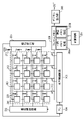
画素アレイ(画素アレイ領域)200には、複数の単位画素(画素)201が行列状に配されている。ここでは、説明を簡単にするために、4×4の単位画素201の配列が図示されているが、実際には、多数の単位画素201が画素アレイ200に配されている。単位画素201は、当該単位画素201に入射したフォトンをカウントし、カウントによって得られたデジタルの信号を出力することが可能である。この点の詳細については、図3を用いて後述する。
A plurality of unit pixels (pixels) 201 are arranged in a matrix in a pixel array (pixel array region) 200 . Although the arrangement of 4×4
飽和検出部205は、画素アレイ200に備えられた複数の単位画素201のうちのいずれかにおいてフォトンのカウント値が露光期間中に所定の閾値Cthに達したことを検出する。複数の単位画素201のうちのいずれかにおいてフォトンのカウント値が閾値Cthに達したことを検出すると、飽和検出部205は、その旨を示す情報をタイミングジェネレータ204に供給する。
The
フォトンのカウント値が閾値Cthに達した単位画素201は、フォトンのカウント値が閾値Cthに達したことを示す信号である閾値到達信号PSAT(図3参照)を、配線212を介して飽和検出部205に出力する。閾値到達信号PSATは、行毎に備えられた共通の配線212を介して飽和検出部205に送信される。各々の配線212には、プルアップ抵抗211がそれぞれ接続されている。プルアップ抵抗211の一端は配線212に接続されており、プルアップ抵抗211の他端は電源電圧VDDに接続されている。
The
なお、ここでは、行毎に備えられた共通の配線212を介して閾値到達信号PSATが飽和検出部205に出力される場合を例に説明したが、これに限定されるものではない。例えば、列毎に備えられた共通の配線を介して閾値到達信号PSATが飽和検出部205に送信されるようにしてもよい。また、全ての単位画素201に対して共通に備えられた配線を介して閾値到達信号PSATが飽和検出部205に出力されるようにしてもよい。
Although the case where the threshold reaching signal PSAT is output to the
閾値到達信号PSATが露光期間中に飽和検出部205に供給されると、飽和検出部205は当該閾値到達信号PSATを検出し、閾値到達信号PSATを検出したことを示す信号をタイミングジェネレータ204に送信する。タイミングジェネレータ204は、閾値到達信号PSATが検出されたことを示す信号を飽和検出部205から受け取ると、各々の単位画素201から画素信号を出力させるための制御信号を、垂直制御回路202及び水平制御回路203に対して供給する。なお、タイミングジェネレータ204は、不図示の配線を介して、フレームメモリ206、加算回路207、デジタル出力部208に、制御信号をそれぞれ供給する。
When the threshold reaching signal PSAT is supplied to the
垂直制御回路202は、画素アレイ200に備えられた複数の単位画素201をスイッチ209によって行単位で選択する。また、垂直制御回路202は、画素アレイ200に備えられた複数の単位画素201に対して、不図示の配線を介して行毎に制御信号を供給する。制御信号の詳細については、図3を用いて後述する。
The
水平制御回路203は、画素アレイ200に備えられた複数の単位画素201をスイッチ210によって列単位で選択する。
The
垂直制御回路202と水平制御回路203との組み合わせによって順次選択される単位画素201からの画素信号が、フレームメモリ206に保持される。
Pixel signals from the
フレームメモリ206は、各々の単位画素201から出力されるデジタルの画素信号を保持する。フレームメモリ206は、一時メモリ領域206aと積算メモリ領域206bとを備えている。
A
一時メモリ領域206aは、各々の単位画素201から出力されるデジタルの画素信号を一時的に保持する。積算メモリ領域206bは、露光期間中に一時メモリ領域206aに保持された画素信号を同一アドレス毎(同一画素毎)に積算し、積算により得られた画素信号を保持する。一時メモリ領域206aに保持される画素信号(データ)のビット幅は、単位画素201から出力されるデジタルの画素信号のビット幅と同等とすることができる。一方、積算メモリ領域206bに保持される画素信号のビット幅は、単位画素201から出力されるデジタルの画素信号のビット幅に対して十分に大きい。
The
加算回路207は、フレームメモリ206の積算メモリ領域206bに保持されている画素信号と、フレームメモリ206の一時メモリ領域206aに新たに保持された画素信号とを加算する。加算回路207は、このような加算処理を同一アドレス毎(同一画素毎)に行う。加算回路207によって行われる加算によって得られる画素信号は、積算メモリ領域206bに保持される。こうして、積算メモリ領域206bに保持される画素信号が更新される。
The
デジタル出力部208は、フレームメモリ206の積算メモリ領域206bに保持された画素信号(画像信号、撮像信号)を固体撮像素子100の外部に出力する。
The
なお、ここでは、フレームメモリ206及び加算回路207が固体撮像素子100に備えられている場合を例に説明したが、これに限定されるものではない。フレームメモリ206及び加算回路207を固体撮像素子100の外部に設けるようにしてもよい。
Here, the case where the
図3は、本実施形態による固体撮像素子に備えられた単位画素を示す図である。図3に示すように、単位画素201には、センサ部(受光部)301と、計数部302とが備えられている。センサ部301には、フォトダイオード303と、クエンチ抵抗304と、反転バッファ305とが備えられている。フォトダイオード303は、アバランシェフォトダイオードである。フォトダイオード303のアノードは接地電位に接続されており、フォトダイオード303のカソードはクエンチ抵抗304の一端に接続されている。クエンチ抵抗304の他端にはバイアス電圧(逆バイアス電圧)Vbiasが印加される。フォトダイオード303には、クエンチ抵抗304を介してフォトダイオード303の降伏電圧以上のバイアス電圧Vbiasが印加される。このため、フォトダイオード303は、ガイガーモードで動作する。即ち、フォトダイオード303にフォトンが入射するとアバランシェ増倍現象を引き起こす。これにより、アバランシェ電流が生じ、クエンチ抵抗304において電圧降下が生ずる。クエンチ抵抗304は、フォトダイオード303のアバランシェ増倍現象を停止させるための抵抗素子である。クエンチ抵抗304は、トランジスタの抵抗成分を利用して構成し得る。フォトダイオード303においてアバランシェ増倍現象によってアバランシェ電流が生じると、クエンチ抵抗304において電圧降下が生じ、フォトダイオード303に印加される逆バイアス電圧が降下する。逆バイアス電圧が降伏電圧まで降下するとアバランシェ増倍現象が停止する。その結果、アバランシェ電流が流れなくなり、フォトダイオード303には、再びバイアス電圧Vbiasが印加される。反転バッファ305は、クエンチ抵抗304で発生した電圧変化をパルス信号PLSとして取り出すために設けられる。フォトダイオード303に光子が入射すると、反転バッファ305からパルス信号PLSが出力される。このように、センサ部301からは、フォトンの受光頻度に応じた頻度でパルスが発せられる。
FIG. 3 is a diagram showing a unit pixel provided in the solid-state imaging device according to this embodiment. As shown in FIG. 3 , the
ここで、センサ部301の動作について図4を用いて説明する。図4は、センサ部301の動作を示す図である。図4には、フォトダイオード303にフォトンが入射した際のカソード端子電圧Voutの時間変化と、反転バッファ305から出力されるパルス信号PLSの時間変化とが示されている。図4の横軸は時刻である。カソード端子電圧Voutは、フォトダイオード303に印加される逆バイアス電圧の大きさでもある。
Here, the operation of the
タイミングt401において、フォトダイオード303には、降伏電圧Vbr以上のバイアス電圧Vbiasが印加されている。このため、フォトダイオード303はガイガーモードで動作する。
At timing t401, the
タイミングt402において、フォトダイオード303にフォトンが入射すると、フォトダイオード303において生成されたキャリアがアバランシェ増倍現象を引き起こし、アバランシェ電流が生ずる。このアバランシェ電流によって、クエンチ抵抗304に接続されたフォトダイオード303のカソード端子電圧Voutが低下し始める。
At timing t402, when photons enter the
タイミングt403において、フォトダイオード303のカソード端子電圧Voutは、閾値Vthまで低下し、この後、フォトダイオード303のカソード端子電圧Voutは更に低下し続ける。フォトダイオード303のカソード端子電圧Voutが閾値Vthまで低下するタイミングt403において、反転バッファ305から出力されるパルス信号PLSはLレベルからHレベルに遷移する。
At timing t403, the cathode terminal voltage Vout of the
フォトダイオード303のカソード端子電圧Voutは、タイミングt404において、降伏電圧Vbrまで低下する。フォトダイオード303のカソード端子電圧Voutが降伏電圧Vbrまで低下すると、アバランシェ増倍現象が停止する。そうすると、バイアス電圧Vbiasを供給している電源からクエンチ抵抗304を介して再充電が行われるようになるため、フォトダイオード303のカソード端子電圧Voutは上昇し始める。
The cathode terminal voltage Vout of the
タイミングt405において、フォトダイオード303のカソード端子電圧Voutは閾値Vthまで上昇する。フォトダイオード303のカソード端子電圧Voutが閾値Vthに達するタイミングt405において、反転バッファ305から出力されるパルス信号PLSはHレベルからLレベルに遷移する。
At timing t405, the cathode terminal voltage Vout of the
この後、タイミングt406において、再充電が完了する。再充電が完了した段階では、フォトダイオード303のカソード端子電圧Voutは、バイアス電圧Vbiasに戻っている。なお、再充電に要する時間は、クエンチ抵抗304の抵抗値と寄生容量とに依存する。このように、1回のフォトンの入射によって、パルス幅ΔTpの1つのパルス信号PLSがセンサ部301から出力される。
Thereafter, at timing t406, recharging is completed. At the stage when recharging is completed, the cathode terminal voltage Vout of the
図3に示すように、計数部302には、カウンタ(カウンタ回路)306と、画素メモリ307と、反転バッファ308とが備えられている。
As shown in FIG. 3 , the
カウンタ306には、センサ部301にフォトンが入射することによって生ずるパルス信号PLSが入力され、カウンタ306はパルス信号PLSがLレベルからHレベルに変化した回数をパルス数としてカウントする。カウンタ306によるパルスのカウント値は、画素信号となる。カウンタ306には、パルスをカウントする状態とパルスをカウントしない状態とを切り替えるためのイネーブル制御端子ENが備えられている。また、カウンタ306には、カウンタ306をリセットするためのリセット端子RESが備えられている。カウンタ306のイネーブル制御端子ENには、垂直制御回路202からイネーブル信号PENが供給される。また、カウンタ306のリセット端子RESには、垂直制御回路202からリセット信号PRESが供給される。カウンタ306に供給されるイネーブル信号PENがHレベルの状態で、パルス信号PLSがLレベルからHレベルに変化すると、カウンタ306のカウント値は1つずつ増加する。イネーブル信号PENがLレベルの状態においては、パルス信号PLSがLレベルからHレベルに変化しても、カウンタ306のカウント値は増加しない。また、カウンタ306に供給されるリセット信号PRESがLレベルからHレベルに変化すると、カウンタ306のカウント値は0にリセットされる。
A pulse signal PLS generated by incident photons on the
画素メモリ307は、カウンタ306によってカウントされた画素信号であるカウント値を一時的に保持する。画素メモリ307には、垂直制御回路202からラッチ信号PLATが供給される。ラッチ信号PLATがLレベルからHレベルに変化すると、画素メモリ307は、カウンタ306のカウント値を取り込み、取り込んだカウント値を保持する。画素メモリ307に取り込まれたカウント値は、画素信号として用いられる。
A
垂直制御回路202と水平制御回路203とによって選択される単位画素201の画素メモリ307に保持されているカウント値(画素信号)が、フレームメモリ206に送信される。
A count value (pixel signal) held in the
なお、本実施形態においては、イネーブル信号PEN、リセット信号PRES及びラッチ信号PLATは、画素アレイ200に備えられたすべての単位画素201に対して垂直制御回路202から同時に供給される。
Note that in the present embodiment, the enable signal PEN, reset signal PRES, and latch signal PLAT are simultaneously supplied from the
カウンタ306は、不図示の比較回路を備えている。カウンタ306は、カウント値が所定の閾値Cth以上になった際には、カウント値が閾値Cth以上になったことを示す信号である閾値到達信号PSATをオープンドレイン出力の反転バッファ308を介して出力する。カウント値が閾値Cth未満の状態においては、カウンタ306から反転バッファ308を介して出力される閾値到達信号PSATはハイレベル(Hレベル)である。一方、カウント値が閾値Cth以上になると、カウンタ306から反転バッファ308を介して出力される閾値到達信号PSATはローレベル(Lレベル)となる。上述したように、同一行に位置する単位画素201から出力される閾値到達信号PSATは、共通の配線212を介して出力される。配線212は、プルアップ抵抗211によってプルアップされている。従って、各々の単位画素201から出力される閾値到達信号PSATは、ワイヤードOR接続された状態になっている。
The
同一行に位置する複数の単位画素201のうちのいずれにおいてもカウント値が閾値Cth未満である場合には、配線212を介して飽和検出部205に供給される閾値到達信号PSATはHレベルである。一方、同一行に位置する複数の単位画素201のうちのいずれかにおいてカウント値が閾値Cth以上になった場合には、配線212を介して飽和検出部205に供給される閾値到達信号PSATはLレベルとなる。飽和検出部205には、すべての行から閾値到達信号PSATが供給される。このため、飽和検出部205は、画素アレイ200に備えられた複数の単位画素201のうちのいずれかにおいてカウント値が閾値Cth以上になったことを検出することができる。
When the count value is less than the threshold value Cth for any of the plurality of
図5は、本実施形態による固体撮像素子100のレイアウトの例を示す図である。固体撮像素子100は、複数のセンサ部301が行列状に配されたセンサ部基板501と、複数の計数部302が行列状に配された計数部基板502と、フレームメモリ206が配されたフレームメモリ基板503とを積層させた構成となっている。センサ部基板501に備えられた電極(図示せず)と計数部基板502に備えられた電極(図示せず)とが、互いに電気的に接続されている。また、計数部基板502に備えられた電極(図示せず)とフレームメモリ基板503に備えられた電極(図示せず)とが、互いに電気的に接続されている。こうして、センサ部基板501に備えられたセンサ部301から出力されるパルス信号PLSが、計数部基板502に備えられた計数部302に入力されるようになっている。計数部基板502には、垂直制御回路202、水平制御回路203、タイミングジェネレータ204、及び、飽和検出部205が備えられている。フレームメモリ基板503には、フレームメモリ206、加算回路207、及び、デジタル出力部208が備えられている。センサ部301と計数部302とが別個の基板に備えられているため、センサ部301の面積を広く確保することができる。また、フレームメモリ基板503をセンサ部基板501及び計数部基板502よりも微細なプロセスで製造すれば、フレームメモリ206には十分に大きなビット幅のデータを記録し得る。なお、固体撮像素子100の構成は、上記のような構成に限定されるものではない。例えば、同一の基板にセンサ部301と計数部302とを備えるようにしてもよい。
FIG. 5 is a diagram showing an example layout of the solid-
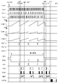
図6は、本実施形態による固体撮像素子の動作の例を示すタイミングチャートである。ここでは、動画像を構成する複数のフレームのうちの1つのフレームの画像を取得する場合を例に説明するが、これに限定されるものではない。 FIG. 6 is a timing chart showing an example of the operation of the solid-state imaging device according to this embodiment. Here, a case of obtaining an image of one frame out of a plurality of frames forming a moving image will be described as an example, but the present invention is not limited to this.
タイミングt601において、撮影開始の指示が操作部108を介してユーザ等によって行われると、制御部104は、固体撮像素子100に対してパルス状の撮影開始信号STARTを供給する。撮影開始信号STARTがHレベルになると、タイミングジェネレータ204はセンサ部301にバイアス電圧Vbiasを供給する。センサ部301にバイアス電圧Vbiasが供給されると、フォトダイオード303の降伏電圧以上の逆バイアス電圧がフォトダイオード303に印加され、フォトダイオード303はガイガーモードで動作するようになる。これにより、センサ部301は、フォトダイオード303に入射するフォトンに応じてパルス信号PLSを出力するようになる。図6には、画素アレイ200に備えられた複数の単位画素201のうちの任意の3つの単位画素201、即ち、単位画素A、B、Cの各々のセンサ部301からそれぞれ出力されるパルス信号PLS_A、PLS_B、PLS_Cが示されている。ここでは、単位画素Aに入射するフォトンの数が単位画素Cに入射するフォトンの数より多く、単位画素Cに入射するフォトンの数が単位画素Bに入射するフォトンの数より多い場合を例に説明する。
At timing t<b>601 , when the user or the like issues an instruction to start imaging via the
図6に示すカウント値COUNT_A、COUNT_B、COUNT_Cは、単位画素A、B、Cの各々のカウンタ306によって得られるカウント値を示している。カウンタ306は、カウント下限値0からカウント上限値Cmaxまでをカウントすることが可能である。カウンタ306のカウント値が閾値Cth以上になると、カウント値が閾値Cth以上になったカウンタ306が備えられている単位画素201から出力される閾値到達信号PSATがHレベルからLレベルに変化する。これにより、当該単位画素201が位置している行に備えられた配線212の電位がHレベルからLowレベルに変化する。HレベルからLレベルに変化した閾値到達信号PSATは、飽和検出部205によって検出される。閾値到達信号PSAT_A、PSAT_B、PSAT_Cは、各々の単位画素A、B、Cが備えられている行における閾値到達信号PSATを示している。
Count values COUNT_A, COUNT_B, and COUNT_C shown in FIG. 6 indicate count values obtained by the
タイミングt601において、リセット信号PRESはHレベルになっている。また、タイミングt601において、各々の単位画素201のカウンタ306は0にリセットされている。
At timing t601, the reset signal PRES is at H level. Also, the
タイミングt602において、タイミングジェネレータ204は、画素アレイ200のすべての行にLレベルのリセット信号PRESを同時に供給する。これにより、画素アレイ200に備えられた全ての単位画素201のカウンタ306のリセットが解除される。また、タイミングジェネレータ204は、画素アレイ200の全ての行にHレベルのイネーブル信号PENを供給する。これにより、画素アレイ200に備えられた全ての単位画素201のカウンタ306はイネーブル状態となり、各々の単位画素201のカウンタ306において、入力されるパルス信号PLSに応じてカウント値が増加するようになる。こうして、動画像を構成する複数のフレームのうちの1つのフレームの撮像が開始される。この後、イネーブル信号PENがLレベルに変化するタイミングt608まで当該フレームにおけるカウントが継続される。従って、タイミングt602からタイミングt608までが、露光期間に相当する。フォトンが入射する頻度は単位画素Aが最も高いため、カウント値COUNT_Aの増加率が最も大きい。
At timing t602, the
タイミングt603において、カウント値COUNT_Aが閾値Cthに達すると、単位画素Aが備えられている行の閾値到達信号PSAT_AがLレベルになる。飽和検出部205は、いずれかの行の閾値到達信号PSATがLレベルに変化したことを検出すると、閾値到達信号PSATが検出されたことを示す信号をタイミングジェネレータ204に対して送信する。閾値到達信号PSATが検出されたことを示す信号をタイミングジェネレータ204が受信すると、タイミングジェネレータ204は、以下のように動作する。即ち、タイミングジェネレータ204は、垂直制御回路202から全ての単位画素201に供給されるラッチ信号PLATが一斉にHレベルとなるように、垂直制御回路202に対して制御信号を供給する。これにより、各々の単位画素201に備えられたカウンタ306のカウント値が、各々のカウンタ306に対応する画素メモリ307にそれぞれ保持される。
At timing t603, when the count value COUNT_A reaches the threshold Cth, the threshold reaching signal PSAT_A of the row in which the unit pixel A is provided becomes L level. When
タイミングt604において、リセット信号PRESがHレベルになると、各々の単位画素201のカウンタ306のカウント値が0にリセットされる。そして、リセット信号PRESがLレベルに戻ると、カウンタ306のリセットが解除され、各々の単位画素201のカウンタ306は、再び入射したフォトンに応じてカウントを開始する。また、単位画素Aのカウント値が0にリセットされたことにより、閾値到達信号PSAT_AはLレベルからHレベルに戻る。
At timing t604, when the reset signal PRES becomes H level, the count value of the
タイミングt605において、タイミングジェネレータ204から垂直制御回路202に対して信号VCLKの供給が開始される。信号VCLKがHレベルになる毎に、各行のスイッチ209が順次オン状態となり、画素アレイ200に備えられた複数の単位画素201を垂直制御回路202が1行ずつ選択していく。任意の1行が垂直制御回路202によって選択されると、タイミングジェネレータ204から水平制御回路203に信号HCLKが供給され、各列のスイッチ210を順次オン状態にする。これにより、選択行の単位画素201の画素メモリ307に保持されていたカウント値(画素信号)がフレームメモリ206の一時メモリ領域206aに順次格納される。そして、加算回路207は、フレームメモリ206の一時メモリ領域206aに保持された画素信号と、フレームメモリ206の積算メモリ領域206bに保持されている同一アドレスの画素信号とを加算する。そして、加算回路207は、加算することにより得られる画素信号を積算メモリ領域206bに再び格納する。なお、フレームメモリ206による画素信号の保持と並行して、加算回路207による加算処理が行われる。タイミングt605~t606において行われる加算処理、即ち、最初の加算処理においては、フレームメモリ206の積算メモリ領域206bには画素信号が保持されていない。このため、各々の単位画素201から出力されて一時メモリ領域206aに格納された画素信号は、そのまま積算メモリ領域206bに保持される。
At timing t<b>605 , the
タイミングt607において、カウント値COUNT_Aが再び閾値Cthに達すると、閾値到達信号PSAT_AがLレベルとなる。そして、タイミングt603~t606の際と同様に、各々の単位画素201の画素信号がフレームメモリ206の一時メモリ領域206aに格納される。そして、一時メモリ領域206aに格納された画素信号と積算メモリ領域206bに保持されている画素信号とが加算され、加算により得られた画素信号が積算メモリ領域206bに格納される。この後も、いずれかの単位画素201のカウント値が露光期間中に閾値Cthに達するたびに上記と同様の処理が繰り返される。
At timing t607, when the count value COUNT_A reaches the threshold Cth again, the threshold reaching signal PSAT_A becomes L level. Then, the pixel signal of each
このように、タイミングt605~t606においては、各々の単位画素201の画素メモリ307に保持されているカウント値(画素信号)が、フレームメモリ206の一時メモリ領域206aに順次格納される。各々の単位画素201の画素メモリ307に保持されているカウント値をフレームメモリ206の一時メモリ領域206aに格納する処理は、単位画素201のカウント値が再び閾値Cthに達するタイミングt607より前に完了していることが好ましい。パルス信号PLSのパルス幅をΔTpとすると、カウント値が0から閾値Cthに達するまでの時間は、最短でΔTp×Cthである。従って、各々の単位画素201のカウント値をフレームメモリ206の一時メモリ領域206aに格納する処理が(ΔTp×Cth)よりも短い時間で完了するように、信号VCLK、HCLKの周波数を設定することが好ましい。また、各々の単位画素201のカウント値をフレームメモリ206の一時メモリ領域206aに格納する処理に要する時間よりも(ΔTp×Cth)が長くなるように、カウンタ306の閾値Cthを設定するようにしてもよい。
In this manner, the count values (pixel signals) held in the
タイミングt608において、露光期間が終了すると、イネーブル信号PENがLレベルとなる。これにより、各々の単位画素201のカウンタ306がディセーブル状態となり、カウンタ306にパルス信号PLSが入力されてもカウント値が増加しなくなる。また、センサ部301に対してバイアス電圧Vbiasが供給されなくなり、センサ部301はパルス信号PLSを出力しなくなる。
At timing t608, when the exposure period ends, the enable signal PEN becomes L level. As a result, the
この後、タイミングジェネレータ204は、露光終了時におけるカウンタ306のカウント値をフレームメモリ206に格納するために、以下のような処理を行う。即ち、タイミングジェネレータ204は、タイミングt609において、ラッチ信号PLATをLレベルからHレベルに変化させる。ラッチ信号PLATがLレベルからHレベルに変化すると、画素メモリ307は、カウンタ306のカウント値を取り込み、取り込んだカウント値を保持する。この後、タイミングジェネレータ204から供給されたラッチ信号PLATを、HレベルからLレベルに戻す。また、タイミングジェネレータ204は、リセット信号PRES信号をHレベルにし、カウンタ306のカウント値を0にリセットする。
After that, the
タイミングt610~t611においては、タイミングt605~606と同様に、各々の単位画素201の画素信号がフレームメモリ206の一時メモリ領域206aに保持される。そして、加算回路207によって加算処理された画素信号がフレームメモリ206の積算メモリ領域206bに保持される。積算メモリ領域206bに保持される画素信号は、タイミングt602~t608の露光期間中に画素メモリ307から取得される画素信号を加算回路207によって積算することにより得られる信号である。こうして得られる画素信号は、露光期間中に入射したフォトンの数に応じた信号となる。このように、本実施形態によれば、カウンタ306のカウント値が露光期間中に飽和するのを防止することができる。
At timings t610 to t611, the pixel signal of each
なお、画素メモリ307に保持されている画素信号をフレームメモリ206の一時メモリ領域206aに順次送信している最中に、露光終了のタイミングt608が到来する場合もある。このような場合には、各々の単位画素201の画素メモリ307に保持されている画素信号をフレームメモリ206の一時メモリ領域206aに格納し終わってから、露光終了時のカウンタ306のカウント値を画素メモリ307に格納するようにすればよい。
It should be noted that while the pixel signals held in the
タイミングt612~t613では、タイミングジェネレータ204からデジタル出力部208に制御信号OUTCLKが供給される。これにより、フレームメモリ206の積算メモリ領域206bに保持された画素信号、即ち、露光期間中に積算された画素信号が、デジタル出力部208を介して固体撮像素子100の外部に順次出力される。固体撮像素子100の外部への画素信号の出力が完了すると、フレームメモリ206の積算メモリ領域206bに保持されている画素信号は0にリセットされる。
The control signal OUTCLK is supplied from the
このように、本実施形態では、各々の単位画素201のカウンタ306のカウント値が閾値Cthに達するたびに、カウント値の取得及びリセット動作が行われる。このため、本実施形態によれば、カウント値が露光期間中に飽和するのを防止することができ、階調の良好な画像を得ることができる。
Thus, in the present embodiment, each time the count value of the
なお、上述したように、タイミングt603においてラッチ信号PLATがHレベルになると、カウンタ306のカウント値が画素メモリ307に保持される。そして、タイミングt604においてリセット信号PRESがLレベルからHレベルに変化し、カウンタ306がリセットされる。そして、リセット信号PRESがHレベルからLレベルに戻ると、カウンタ306のリセットが解除される。このように、ラッチ信号PLATがHレベルになるタイミングt603からカウンタ306のリセットが解除されるタイミングまでの期間は、パルス信号PLSの数をカウンタ306によってカウントできなくなる。このことは、当該期間の分だけ露光期間が短くなったことに相当する。従って、この期間の分だけ露光期間を延長するようにしてもよい。
As described above, when the latch signal PLAT becomes H level at timing t603, the count value of the
また、図6に示すような駆動モード(第1の駆動モード)と異なる駆動モード(第2の駆動モード)で固体撮像素子100を駆動できるようにしてもよい。第2の駆動モードにおいては、例えば、飽和検出部205の動作を無効とする。第2の駆動モードでは、カウンタ306によって露光期間中にカウントされるカウント値は、露光期間中にはフレームメモリ206に出力されない。第2の駆動モードでは、カウンタ306によるカウント値が、露光期間が終了した後にフレームメモリ206に出力される。例えば、高照度環境下においては、第1の駆動モードで固体撮像素子100を駆動し、低照度環境下においては、第2の駆動モードで固体撮像素子100を駆動するようにしてもよい。
Further, the solid-
[第2実施形態]
第2実施形態による固体撮像素子、撮像装置及び撮像方法を図7乃至図9を用いて説明する。なお、図1乃至図6に示す第1実施形態による固体撮像素子等と同一の構成要素には、同一の符号を付して説明を省略又は簡潔にする。
[Second embodiment]
A solid-state imaging device, an imaging apparatus, and an imaging method according to the second embodiment will be described with reference to FIGS. 7 to 9. FIG. The same components as those of the solid-state imaging device according to the first embodiment shown in FIGS. 1 to 6 are denoted by the same reference numerals, and the description thereof is omitted or simplified.
本実施形態による固体撮像素子は、各々の単位画素701の計数部801に画素メモリ307(図3参照)が備えられていないものである。
In the solid-state imaging device according to this embodiment, the pixel memory 307 (see FIG. 3) is not provided in the
図7は、第2実施形態による固体撮像素子100を示す図である。画素アレイ200には、複数の単位画素701が備えられている。垂直制御回路202は、画素アレイ200に備えられた複数の単位画素701をスイッチ209によって行単位で選択する。スイッチ209は、垂直制御回路202から配線703を介して供給される行選択信号PSELによって行単位で制御される。
FIG. 7 is a diagram showing a solid-
画素アレイ200と水平制御回路203との間には、列メモリ702が備えられている。列メモリ702は、垂直制御回路202によって行単位で選択される単位画素701から出力される各列の画素信号を一時的に保持する。
A
図8は、本実施形態による固体撮像素子に備えられた単位画素701を示す図である。図8に示すように、単位画素701には、センサ部301と、計数部801とが備えられている。計数部801には、カウンタ306と、反転バッファ308とが備えられている。計数部801には、画素メモリ307(図3参照)は備えられていない。計数部801に画素メモリ307が備えられていないため、本実施形態では、カウンタ306のカウント値が画素メモリ307を介することなく列メモリ702に行単位で保持される。
FIG. 8 is a diagram showing a
カウンタ306のリセット端子RESには、垂直制御回路202からリセット信号PRESが行単位で供給される。従って、カウンタ306のカウント値は行単位でリセットされる。
A reset signal PRES is supplied from the
図9は、本実施形態による固体撮像素子の動作を示すタイミングチャートである。ここでは、動画像を構成する複数のフレームのうちの1つのフレームの画像を取得する場合を例に説明するが、これに限定されるものではない。 FIG. 9 is a timing chart showing the operation of the solid-state imaging device according to this embodiment. Here, a case of obtaining an image of one frame out of a plurality of frames forming a moving image will be described as an example, but the present invention is not limited to this.
図9には、画素アレイ200に備えられた複数の単位画素701のうちの任意の2つの単位画素701、即ち、単位画素D、Eの各々のセンサ部301からそれぞれ出力されるパルス信号PLS_D、PLS_Eが示されている。単位画素Dは、画素アレイ200の第1番目の行に配されており、画素信号の出力時には最初に読み出される。一方、単位画素Eは、画素アレイ200の最終行に配されており、画素信号の出力時には最後に読み出される。ここでは、単位画素Eに入射するフォトンの数が最も多い場合を例に説明する。
FIG. 9 shows two
図9に示すカウント値COUNT_D、COUNT_Eは、単位画素D、Eの各々のカウンタ306によって得られるカウント値を示している。カウンタ306は、カウント下限値0からカウント上限値Cmaxまでをカウントすることが可能である。カウンタ306のカウント値が閾値Cth以上になると、カウント値が閾値Cth以上になったカウンタ306が備えられている単位画素701から出力される閾値到達信号PSATがHレベルからLレベルに変化する。これにより、当該単位画素701が位置している行に備えられた配線212の電位がHレベルからLowレベルに変化する。HレベルからLレベルに変化した閾値到達信号PSATは、飽和検出部205によって検出される。閾値到達信号PSAT_D、PSAT_Eは、各々の単位画素D、Eが備えられている行における閾値到達信号PSATを示している。行選択信号PSEL_Dは、単位画素Dが配されている行、即ち、画素アレイ200の第1番目の行に供給される。行選択信号PSEL_Eは、単位画素Eが配されている行、即ち、画素アレイ200の最終行に供給される。行選択信号PSELがHレベルになると、対応する行のスイッチ209がオン状態になる。スイッチ209がオン状態になると、当該スイッチ209に対応する単位画素701のカウンタ306のカウント値が列メモリ702に出力され、当該カウント値が列メモリ702によって保持される。リセット信号PRES_Dは、単位画素Dが配されている行、即ち、画素アレイ200の第1番目の行に供給される。リセット信号PRES_Eは、単位画素Eが配されている行、即ち、画素アレイ200の最終行に供給される。リセット信号PRESがHレベルになると、対応する行のカウンタ306のカウント値が0にリセットされる。
Count values COUNT_D and COUNT_E shown in FIG. 9 indicate count values obtained by the
出力開始信号PVSTは、各々の単位画素701において取得されたカウント値の列メモリ702への出力を開始するための信号であり、タイミングジェネレータ204から垂直制御回路202に供給される。出力開始信号PVSTがLレベルからHレベルに変化すると、カウンタ306によって得られたカウント値を列メモリ702に出力する動作と、カウンタ306をリセットする動作とが、画素アレイ200の第1番目の行から順に行単位で行われる。
The output start signal PVST is a signal for starting outputting the count value obtained in each
タイミングt901において、撮影開始の指示が操作部108を介してユーザ等によって行われると、制御部104は、固体撮像素子100に対してパルス状の撮影開始信号STARTを供給する。撮影開始信号STARTがHレベルになると、タイミングジェネレータ204はセンサ部301にバイアス電圧Vbiasを供給する。センサ部301にバイアス電圧Vbiasが供給されると、フォトダイオード303の降伏電圧以上のバイアス電圧がフォトダイオード303に印加され、フォトダイオード303はガイガーモードで動作するようになる。これにより、センサ部301は、フォトダイオード303に入射するフォトンに応じてパルス信号PLSを出力するようになる。
At timing t<b>901 , when the user or the like issues an instruction to start imaging via the
タイミングt901において、リセット信号PRESはHレベルになっている。また、タイミングt901において、各々の単位画素701のカウンタ306は0にリセットされている。
At timing t901, the reset signal PRES is at H level. Also, the
タイミングt902において、タイミングジェネレータ204は、画素アレイ200のすべての行にLレベルのリセット信号PRESを同時に供給する。これにより、画素アレイ200に備えられた全ての単位画素701のカウンタ306のリセットが解除される。また、タイミングジェネレータ204は、画素アレイ200の全ての行にHレベルのイネーブル信号PENを供給する。これにより、画素アレイ200に備えられた全ての単位画素701のカウンタ306はイネーブル状態となり、各々の単位画素701のカウンタ306において、入力されるパルス信号PLSに応じてカウント値が増加するようになる。この後、イネーブル信号PENがLレベルに変化するタイミングt909まで当該フレームにおけるカウントが継続される。従って、タイミングt902からタイミングt909までが、露光期間に相当する。フォトンが入射する頻度は単位画素Eが最も高いため、カウント値COUNT_Eの増加率が最も大きい。
At timing t902, the
タイミングt903において、カウント値COUNT_Eが閾値Cthに達すると、単位画素Eが備えられている行の閾値到達信号PSAT_EがLレベルになる。飽和検出部205は、いずれかの行の閾値到達信号PSATがLレベルに変化したことを検出すると、パルス状の出力開始信号PVSTを出力し、これにより画素信号の読み出しの動作が開始される。
At timing t903, when the count value COUNT_E reaches the threshold Cth, the threshold reaching signal PSAT_E of the row in which the unit pixel E is provided becomes L level. When the
タイミングt904において、画素アレイ200の第1番目の行にパルス状の行選択信号PSEL_Dが供給されると、単位画素Dが配された行である第1番目の行に配された各々の単位画素701のカウント値が列メモリ702に出力される。そして、画素アレイ200の第1番目の行にパルス状のリセット信号PRES_Dが供給されると、単位画素Dが配された行である第1番目の行に配された各々の単位画素701のカウント値が0にリセットされる。このような動作と並行して、タイミングジェネレータ204から水平制御回路203に信号HCLK信号が供給され、各列のスイッチ210を順次オン状態にする。これにより、列メモリ702に保持されていたカウント値、即ち、第1番目の行に位置する単位画素701によって取得された画素信号が、フレームメモリ206に順次出力され、当該画素信号はフレームメモリ206の一時メモリ領域206aに保持される。
At timing t904, when the pulse-shaped row selection signal PSEL_D is supplied to the first row of the
第1番目の行に位置する単位画素701によって取得された画素信号の全てが列メモリ702からフレームメモリ206に転送されると、画素アレイ200の2番目の行にパルス状の行選択信号PSELが供給され、この後も、上記と同様の動作が順次行われる。即ち、カウンタ306によって得られたカウント値を列メモリ702に出力する動作と、カウンタ306をリセットする動作とが順次行われる。このような動作が、画素アレイ200の最終行まで繰り返される。画素信号のフレームメモリ206への格納と並行して、加算回路207によって以下のような処理が行われる。即ち、フレームメモリ206の一時メモリ領域206aに保持された画素信号と、フレームメモリ206の積算メモリ領域206bに保持された同一アドレスの画素信号との加算処理が加算回路207によって行われる。加算回路207による加算によって得られた画素信号は、フレームメモリ206の積算メモリ領域206bに保持される。
When all the pixel signals obtained by the
タイミングt905において、画素アレイ200の最終行にパルス状の行選択信号PSEL_Eが供給されると、単位画素Eが配された行である最終行に配された各々の単位画素701のカウント値が列メモリ702に出力される。そして、タイミングt906において、画素アレイ200の最終行にパルス状のリセット信号PRES_Eが供給されると、単位画素Eが配された行である最終行に配された各々の単位画素701のカウント値が0にリセットされる。タイミングt906においては、単位画素Eが配された行である最終行の閾値到達信号PSAT_EがLレベルからHレベルに戻る。
At timing t905, when the pulse-like row selection signal PSEL_E is supplied to the last row of the
タイミングt907においては、画素アレイ200の最終行に位置する単位画素701から出力される画素信号がフレームメモリ206に格納される。画素アレイ200の最終行に位置する単位画素701から出力される画素信号に対して加算回路207による加算処理が完了すると、画素アレイ200の全ての単位画素701から出力される画素信号のフレームメモリ206への格納が完了する。
At timing t<b>907 , pixel signals output from the
タイミングt903からt907までの期間においては、単位画素701から出力される画素信号のフレームメモリ206への格納が完了していないため、タイミングジェネレータ204は新たな出力開始信号PVST信号を垂直制御回路202に供給しない。
During the period from timing t903 to t907, the pixel signal output from the
タイミングt904~t907において行われる加算処理、即ち、最初の加算処理においては、フレームメモリ206の積算メモリ領域206bには画素信号が保持されていない。このため、各々の単位画素701から出力されて一時メモリ領域206aに格納された画素信号が、そのまま積算メモリ領域206bに保持される。
In addition processing performed at timings t904 to t907, that is, in the first addition processing, the
タイミングt908において、カウント値COUNT_Eが再び閾値Cthに達すると、単位画素Eが備えられている行の閾値到達信号PSAT_EがLレベルになる。そして、タイミングt903~t907の処理と同様に、各々の単位画素701の画素信号がフレームメモリ206の一時メモリ領域206aに格納される。そして、一時メモリ領域206aに格納された画素信号と積算メモリ領域206bに保持されている画素信号とが加算回路207によって加算され、加算により得られた画素信号が積算メモリ領域206bに格納される。この後も、いずれかの単位画素701のカウント値が露光期間中に閾値Cthに達するたびに上記と同様の処理が繰り返される。
At timing t908, when the count value COUNT_E reaches the threshold Cth again, the threshold reaching signal PSAT_E for the row in which the unit pixel E is provided becomes L level. Then, the pixel signal of each
なお、画素アレイ200の最終行に配された単位画素Eのカウント値COUNT_Eは、タイミングt903において閾値Cthに達した後も、入射したフォトンの数に応じてタイミングt906まで増加し続ける。即ち、画素アレイ200の最終行に配された単位画素701から出力される画素信号のフレームメモリ206への格納が完了し、カウンタ306がリセットされるまで、カウンタ306のカウント値は増加する。画素アレイ200に備えられた全ての単位画素701の画素信号のフレームメモリ206への格納が完了する前に、最終行の単位画素701のカウント値がカウント上限値Cmaxに達しないようにすべく、閾値Cthを以下の式(1)を満たすように設定する。
Note that the count value COUNT_E of the unit pixels E arranged in the last row of the
Cth < Cmax-Trd/ΔTp ・・・(1) Cth<Cmax−Trd/ΔTp (1)
ここで、Trdは、タイミングt903からタイミングt906までの期間に対応している。即ち、Trdは、出力開始信号PVSTが供給されるタイミングから、画素アレイ200の最終行に位置する単位画素701に対してリセット信号PRES_Eが供給されるまでの期間である。ΔTpは、センサ部301から出力されるパルス信号PLSの最小のパルス幅である。
Here, Trd corresponds to the period from timing t903 to timing t906. That is, Trd is a period from the timing when the output start signal PVST is supplied until the reset signal PRES_E is supplied to the
なお、上記の(1)では、閾値Cthを一律に設定したが、これに限定されるものではない。例えば、以下の式(2)のように、閾値Cthを行毎に異ならせてもよい。 Although the threshold value Cth is uniformly set in (1) above, the present invention is not limited to this. For example, the threshold value Cth may be different for each row, as shown in Equation (2) below.
Cth(n) < Cmax-T1h×n/ΔTp ・・・(2) Cth(n)<Cmax−T1h×n/ΔTp (2)
ここで、nは、第n番目の行であることを示している。Cth(n)は、第n番目の行の閾値Cthを示している。T1hは、1行分の画素信号をフレームメモリ206に転送するのに要する時間を示している。即ち、T1hは、ある行に対する行選択信号PSEL信号がHレベルになってから次の行に対する行選択信号PSELがHレベルになるまでの時間に相当する。
Here, n indicates the nth row. Cth(n) indicates the threshold value Cth of the nth row. T1h indicates the time required to transfer the pixel signals for one row to the
タイミングt909において、露光期間が終了すると、イネーブル信号PENはLレベルとなる。これにより、各々の単位画素701のカウント値は、フォトンが当該単位画素701に入射しても増加しなくなる。また、タイミングt909において、センサ部301にバイアス電圧Vbiasが供給されなくなり、センサ部301はパルス信号PLSを出力しなくなる。
At timing t909, when the exposure period ends, the enable signal PEN becomes L level. As a result, the count value of each
この後、タイミングジェネレータ204は、露光終了時におけるカウンタ306のカウント値をフレームメモリ206に格納するために、以下のような処理を行う。即ち、タイミングジェネレータ204は、タイミングt910において、パルス状の出力開始信号PVSTを出力する。これにより、タイミングt903~t907と同様に、各々の単位画素701の画素信号がフレームメモリ206の一時メモリ領域206aに保持される。そして、加算回路207によって加算処理された画素信号がフレームメモリ206の積算メモリ領域206bに保持される。
After that, the
積算メモリ領域206bに保持される画素信号は、タイミングt902~t909の露光期間中にカウンタ306から取得される画素信号を加算回路207によって積算することにより得られる信号である。こうして得られる画素信号は、露光期間中に入射したフォトンの数に応じた信号となる。このように、本実施形態によっても、カウンタ306のカウント値が露光期間中に飽和するのを防止することができる。
The pixel signal held in the
タイミングt911~t912では、タイミングジェネレータ204からデジタル出力部208に制御信号OUTCLKが供給される。これにより、フレームメモリ206の積算メモリ領域206bに保持された画素信号、即ち、露光期間中に積算された画素信号が、デジタル出力部208を介して固体撮像素子100の外部に順次出力される。固体撮像素子100の外部への画素信号の出力が完了すると、フレームメモリ206の積算メモリ領域206bに保持されている画素信号は0にリセットされる。
The control signal OUTCLK is supplied from the
このように、本実施形態においても、各々の単位画素201のカウンタ306のカウント値が閾値Cthに達するたびに、カウント値の取得及びリセット動作が行われる。このため、本実施形態においても、カウント値が露光期間中に飽和するのを防止することができ、階調の良好な画像を得ることができる。
Thus, in this embodiment as well, the count value acquisition and reset operation are performed each time the count value of the
[第3実施形態]
第3実施形態による固体撮像素子、撮像装置及び撮像方法を図10及び図11を用いて説明する。なお、図1乃至図9に示す第1又は第2実施形態による固体撮像素子等と同一の構成要素には、同一の符号を付して説明を省略又は簡潔にする。
[Third embodiment]
A solid-state imaging device, an imaging apparatus, and an imaging method according to the third embodiment will be described with reference to FIGS. 10 and 11. FIG. The same components as those of the solid-state imaging device according to the first or second embodiment shown in FIGS. 1 to 9 are denoted by the same reference numerals, and the description thereof is omitted or simplified.
本実施形態による固体撮像素子は、飽和検出部1104、加算回路1105及び積算メモリ1106が単位画素1101に備えられているものである。
The solid-state imaging device according to the present embodiment includes a
図10は、本実施形態による固体撮像素子100を示す図である。画素アレイ200には、複数の単位画素1101が行列状に配されている。
FIG. 10 is a diagram showing a solid-
図11は、本実施形態による固体撮像素子に備えられた単位画素1101を示す図である。
FIG. 11 is a diagram showing a
単位画素1101には、センサ部301と、計数部1102と、積算部1103とが備えられている。
A
計数部1102には、カウンタ306と、画素メモリ307と、飽和検出部1104とが備えられている。カウンタ306のカウント値が露光期間中に所定の閾値Cthに達すると、閾値到達信号PSATがLレベルからHレベルに変化する。カウンタ306から出力される閾値到達信号PSATは、飽和検出部1104に供給されるようになっている。飽和検出部1104は、閾値到達信号PSATがLレベルからHレベルに変化すると、画素メモリ307にラッチ信号PLATを供給する。飽和検出部1104から画素メモリ307にラッチ信号PLATが供給されると、カウンタ306によって取得されたカウント値が画素メモリ307によって保持される。この後、飽和検出部1104は、ORゲート1107の一方の入力端子にリセット信号を供給する。これにより、飽和検出部1104から出力されるリセット信号は、ORゲート1107を介してカウンタ306のリセット端子RESに供給される。飽和検出部1104からORゲート1107を介してカウンタ306にリセット信号が供給されると、カウンタ306はカウント値をリセットする。垂直制御回路202から供給されるリセット信号PRESが、ORゲート1107の他方の入力端子に供給されるようになっている。また、垂直制御回路202から出力されるリセット信号PRESも、ORゲート1107を介してカウンタ306のリセット端子RESに入力される。このため、カウンタ306は、飽和検出部1104から供給されるリセット信号によってリセットされると共に、垂直制御回路202から供給されるリセット信号PRESによってもリセットされる。
The
積算部1103には、加算回路1105と、積算メモリ1106とが備えられている。加算回路1105は、図2を用いて上述した加算回路207に相当する。積算メモリ1106は、図2を用いて上述したフレームメモリ206の積算メモリ領域206bに相当する。積算メモリ1106は、画素メモリ307に保持された画素信号を露光期間中に積算して保持する。積算メモリ1106のビット幅は、カウンタ306のビット幅に対して十分に大きく、また、画素メモリ307のビット幅に対しても十分に大きい。
The integrating
飽和検出部1104は、画素メモリ307にラッチ信号PLATを供給した後、加算回路1105に加算制御信号PADDを供給する。飽和検出部1104から加算回路1105に加算制御信号PADDが供給されると、加算回路1105は、画素メモリ307に保持された画素信号と積算メモリ1106に保持された画素信号とを加算する。そして、加算回路1105は、加算することにより得られた画素信号を積算メモリ1106に保持する。
After supplying the latch signal PLAT to the
各々の単位画素1101の積算メモリ1106に保持された画素信号は、露光期間が終了した後、垂直制御回路202と水平制御回路203とによる制御に応じて、デジタル出力部208に順次出力される。このような動作は、第1実施形態における動作と同様であるため、詳細な説明は省略する。
The pixel signals held in the
このように、各々の単位画素1101に飽和検出部1104、加算回路1105及び積算メモリ1106が備えられていてもよい。本実施形態においても、カウント値が露光期間中に飽和するのを防止することができ、階調の良好な画像を得ることができる。
In this way, each
[第4実施形態]
第4実施形態による固体撮像素子、撮像装置及び撮像方法について図12を用いて説明する。なお、図1乃至図11に示す第1乃至第3実施形態による固体撮像素子等と同一の構成要素には、同一の符号を付して説明を省略又は簡潔にする。
[Fourth embodiment]
A solid-state imaging device, an imaging apparatus, and an imaging method according to the fourth embodiment will be described with reference to FIG. The same components as those of the solid-state imaging devices and the like according to the first to third embodiments shown in FIGS.
本実施形態による固体撮像素子は、欠陥のある単位画素である欠陥画素から好ましくない閾値到達信号PSATが出力されるのを防止し得るものである。 The solid-state imaging device according to this embodiment can prevent a defective pixel, which is a defective unit pixel, from outputting an unfavorable threshold reaching signal PSAT.
フォトダイオード303に結晶欠陥が存在すると、結晶欠陥に起因して暗電流が生じ、フォトダイオード303にフォトンが入射していないにもかかわらず、アバランシェ増倍現象が当該フォトダイオード303において生ずる場合がある。結晶欠陥が存在するフォトダイオード303が備えられたセンサ部301においては、フォトンがフォトダイオード303に入射していないにもかかわらず、パルス信号PLSが高頻度で出力され得る。このような欠陥のあるフォトダイオード303が備えられた単位画素は、欠陥画素と称される。
If there is a crystal defect in the
図12(a)は、本実施形態による固体撮像素子に備えられた単位画素1201を示す図である。画素アレイ200には、複数の単位画素1201が行列状に配されている。本実施形態による固体撮像素子の構成は、単位画素1201以外は、第1実施形態による固体撮像素子と同様である。
FIG. 12A is a diagram showing a
単位画素1201には、センサ部301と、計数部1202とが備えられている。計数部1202には、カウンタ306と、画素メモリ307と、欠陥制御部1203と、イネーブル端子付きの反転バッファ1204とが備えられている。カウンタ306から出力される閾値到達信号PSATは、反転バッファ1204を介して出力される。欠陥制御部1203から反転バッファ1204に供給されるイネーブル信号がLレベルである場合、反転バッファ1204はオフ状態となる。反転バッファ1204がオフ状態の場合、当該反転バッファ1204の出力は常にハイインピーダンスとなり、当該反転バッファ1204からは閾値到達信号PSATが出力されない。一方、欠陥制御部1203から反転バッファ1204に供給されるイネーブル信号がHレベルである場合、反転バッファ1204はオン状態となる。反転バッファ1204がオン状態の場合、当該反転バッファ1204は、図3を用いて上述した反転バッファ308と同様に動作し得る。
A
欠陥制御部1203は、各々の単位画素1201が欠陥画素であるか否かを示す欠陥情報に基づいて、反転バッファ1204にイネーブル信号を供給する。ある単位画素1201が欠陥画素である場合、当該単位画素1201においては、欠陥制御部1203から反転バッファ1204に供給されるイネーブル信号はLレベルとなり、反転バッファ1204はオフ状態となる。一方、当該単位画素1201が欠陥画素でない場合、当該単位画素1201においては、欠陥制御部1203から反転バッファ1204に供給されるイネーブル信号はHレベルとなり、反転バッファ1204はオン状態となる。単位画素1201が欠陥画素であるか否かを示す欠陥情報は、垂直制御回路202及び水平制御回路203を用いて各々の単位画素1201の欠陥制御部1203に予め供給され、各々の単位画素201の欠陥制御部1203においてそれぞれ保持される。欠陥制御部1203と反転バッファ1204とは、当該単位画素1201に備えられたカウンタ306のカウント値が閾値に達したことを示す信号の出力を防止する出力防止手段として機能し得る。
The
欠陥画素である単位画素1201から出力される画素信号は、信号処理部101又は制御部104によって補正処理される。
A pixel signal output from a
なお、ここでは、イネーブル端子付きの反転バッファ1204を計数部1202に設ける場合を例に説明したが、これに限定されるものではない。図12(b)は、本実施形態による固体撮像素子に備えられた単位画素1201の他の例を示す図である。図12(b)に示すように、センサ部301には、フォトダイオード303と、クエンチ抵抗304と、イネーブル端子付きの反転バッファ1205とが備えられている。計数部1202には、カウンタ306と、画素メモリ307と、欠陥制御部1203と、反転バッファ1206が備えられている。計数部1202に備えられた欠陥制御部1203から出力されるイネーブル信号が、センサ部301に備えられたイネーブル端子付きの反転バッファ1205のイネーブル端子に入力される。このように、イネーブル端子付きの反転バッファ1205をセンサ部301に設けるようにしてもよい。欠陥制御部1203と反転バッファ1205とは、当該単位画素1201に備えられたセンサ部301からのパルスの出力を防止する出力防止手段として機能し得る。
Although the case where the inverting
本実施形態によれば、欠陥画素から閾値到達信号PSATが出力されるのを防止し得る。このため、本実施形態によれば、フレームメモリ206への画素信号の転送が欠陥画素に起因して頻発するのを防止することができる。
According to this embodiment, it is possible to prevent the threshold reaching signal PSAT from being output from the defective pixel. Therefore, according to the present embodiment, it is possible to prevent the transfer of pixel signals to the
[第5実施形態]
第5実施形態による固体撮像素子、撮像装置及び撮像方法について図13乃至図18を用いて説明する。なお、図1乃至図12に示す第1乃至第4実施形態による固体撮像素子等と同一の構成要素には、同一の符号を付して説明を省略又は簡潔にする。
[Fifth embodiment]
A solid-state imaging device, an imaging apparatus, and an imaging method according to the fifth embodiment will be described with reference to FIGS. 13 to 18. FIG. The same components as those of the solid-state imaging devices according to the first to fourth embodiments shown in FIGS. 1 to 12 are denoted by the same reference numerals, and the description thereof is omitted or simplified.
本実施形態による撮像装置は、測光部1303を備え、測光部1303からの測光結果に基づいて、図14に示す画素アレイ200の各ブロック1401の閾値到達信号PSATを選択的に無効とするように制御することができる。また、本実施形態による撮像装置は、操作部108を介してユーザー操作によって、閾値到達信号PSATを選択的に無効とするように制御することもできる。
The imaging apparatus according to this embodiment includes a
図14は、本実施形態による固体撮像素子100を示す図である。図14には、画素アレイ200と飽和検出部1403とが抜き出して示されている。画素アレイ200及び飽和検出部1403以外の構成要素については、第1実施形態における固体撮像素子100と同様である。図13においては、説明を簡略化するために4行×4列の16個の単位画素201が図示されているが、実際には多数の単位画素201が画素アレイ200に備えられている。
FIG. 14 is a diagram showing a solid-
図14に示すように、例えば2行×2列の4つの単位画素201によって1つのブロック1401が構成されている。閾値到達信号PSATを伝達する配線1402は、各々のブロック1401において共有されている。各々のブロック1401にそれぞれ備えられた複数の単位画素201のうちのいずれかから出力される閾値到達信号PSATは、配線1402を介して飽和検出部1403に供給される。
As shown in FIG. 14, one
図13に戻り、測光部1303は、不図示のCCDやCMOSなどの測光用の撮像素子を備え、撮影レンズ102を通して入射した光を不図示の可動式ミラー等を介して受光する。測光部1303は、図15に示すような複数の測光エリア1501を備え、測光エリア1501毎に被写体輝度を測定し、その測光結果を制御部104に送る。
Returning to FIG. 13, the
制御部104は、PSAT選択部1301及び駆動設定部1302、現像処理部1304を備える。
The
PSAT選択部1301は、測光部1303からの測光結果を受け取り、画素アレイ200の各ブロック1401の内、閾値到達信号PSATを無効とするブロックを決定する。また、閾値到達信号PSATを無効としなかったブロックでは、閾値到達信号PSATは有効となる。また、PSAT選択部1301は、操作部108を介したユーザー操作によって、選択的に閾値到達信号PSATを無効とするブロックを決定することもできる。画素アレイ200の各ブロックの閾値到達信号PSATを有効とするか無効とするかの情報(以下、PSAT選択情報)は、駆動設定部1302に送信される。
A
駆動設定部1302は、固体撮像素子100及び信号処理部101を制御するための制御信号を送信する。また、PSAT選択部1301から送信されたPSAT選択情報をもとに、画素アレイ200の各ブロック1401の閾値到達信号PSATを有効又は無効にするための制御信号を固体撮像素子100へ送信する。
A
飽和検出部1403では、駆動設定部1302からの制御信号に基づいて、各々のブロック1401から供給される閾値到達信号PSATを有効とするか無効とするかを設定する。あるブロック1401から出力される閾値到達信号PSATを無効とするように飽和検出部1403が設定されている場合、飽和検出部1403は、以下のように動作する。即ち、飽和検出部1403は、当該ブロック1401から飽和検出部1403に閾値到達信号PSATが供給された場合、当該閾値到達信号PSATを無効なものとして取り扱う。従って、当該ブロック1401内に位置する複数の単位画素201のうちのいずれかにおいてカウンタ306のカウント値が閾値Cthに達した場合であっても、ラッチ信号PLATが画素アレイ200の各々の単位画素201に供給されない。このように、飽和検出部1403は、複数の単位画素201のうちの所定の単位画素201に対しては、カウンタ306によるカウント値が閾値に達したことを無視する。一方、あるブロック1401から出力される閾値到達信号PSATを有効とするように飽和検出部1403が設定されている場合、飽和検出部1403は、以下のように動作する。即ち、飽和検出部1403は、当該ブロック1401から飽和検出部1403に閾値到達信号PSATが供給された場合、当該閾値到達信号PSATを有効なものとして取り扱う。従って、当該ブロック1401内に位置する複数の単位画素201のうちのいずれかにおいてカウンタ306のカウント値が閾値Cthに達した場合には、ラッチ信号PLATが画素アレイ200の各々の単位画素201に供給される。
Based on the control signal from the
なお、ここでは、2行×2列の4つの単位画素201が備えられたブロック1401において閾値到達信号PSATが共通化されている場合を例に説明したが、これに限定されるものではない。例えば、ブロック1401に備えられた単位画素201が4つでなくてもよい。また、例えば閾値到達信号PSATを列単位で共通化するようにしてもよい。
Here, the case where the threshold reaching signal PSAT is shared in the
現像処理部1304には、固体撮像素子100から出力され、信号処理部101で各種の補正処理が行われた画像データが入力される。現像処理部1304は、この画像データにデモザイク等の現像処理を行う。現像処理が行われた画像データは、例えば、表示部106に表示される。
Image data output from the solid-
図16は、本実施形態による撮像装置によって取得される画像1600の例を示す図である。ここでは、ブロック1601から供給される閾値到達信号PSATを無効とし、ブロック1601以外から供給される閾値到達信号PSATを有効とする場合を例に説明する。ブロック1601は、太陽に対応している。ブロック1601から供給される閾値到達信号PSATは無効とされているため、ブロック1601については良好な階調の画像信号が得られない。ブロック1601以外から供給される閾値到達信号PSATについては有効とされているため、ブロック1601以外については良好な階調の画像信号が得られる。なお、太陽に対応する画素信号は、飽和していても特段の問題はない。
FIG. 16 is a diagram showing an example of an
図17に、測光部1303からの測光結果をもとに、閾値到達信号PSATを選択的に無効とするように制御して撮影する流れを表すフローチャートを示す。
FIG. 17 is a flow chart showing a flow of photographing by selectively invalidating the threshold attainment signal PSAT based on the photometry result from the
始めに、S1701で、測光部1303が測光を行い、複数の測光エリア1501毎に被写体輝度を測定する。その測光結果は、PSAT選択部1301に送信される。
First, in S<b>1701 , the
次に、S1702で、PSAT選択部1301が、測光部1303からの測光結果をもとに、画素アレイ200の各ブロック1401の中から閾値到達信号PSATを無効とするブロックを決定する。ここでは、被写体輝度がある閾値以上になる測光エリア1501に対応するブロック1401の閾値到達信号PSATを無効とする。これにより、例えば、太陽のように極端に高輝度被写体のあるブロックの閾値到達信号PSATを無効にできる。各ブロックの閾値到達信号PSATを有効とするか無効とするかの情報(PSAT選択情報)は、駆動設定部1302に送信される。
Next, in step S<b>1702 , the
S1703では、駆動設定部1302が、固体撮像素子100及び信号処理部101へ撮像を行うための制御信号を送信する。また、PSAT選択部1301から送信されたPSAT選択情報をもとに、画素アレイ200の各ブロック1401の閾値到達信号PSATを有効又は無効にするための制御信号を固体撮像素子100へ送信する。
In S<b>1703 , the
S1704では、固体撮像素子100が上述したようにして撮像を行う。固体撮像素子100から出力された画像データは、信号処理部101で各種の補正処理が行われ、制御部104に送られる。その後現像処理部1304で現像処理が行われたのち、表示部106に表示される。
In S1704, the solid-
このように、本実施形態によれば、測光部1303の測光結果をもとに、閾値到達信号PSATを選択的に無効とすることができる。例えば、太陽等に対応する単位画素201から発せられる閾値到達信号PSATを選択的に無効とすることができる。このため、本実施形態によれば、例えば太陽に対応する領域以外の領域について階調の良好な画像を得ることができる。
As described above, according to this embodiment, the threshold attainment signal PSAT can be selectively invalidated based on the photometry result of the
また、閾値到達信号PSATを有効にするか無効にするかの切り替えを、操作部108を介してユーザが行うようにしてもよい。
Alternatively, the user may switch between enabling and disabling the threshold reaching signal PSAT via the
図18に、操作部108を介してユーザー操作によって、閾値到達信号PSATを選択的に無効とするように制御して撮影する流れを表すフローチャートを示す。
FIG. 18 is a flow chart showing the flow of photographing by selectively disabling the threshold attainment signal PSAT by user operation via the
始めに、S1801で、固体撮像素子100が撮像を行い、信号処理部101における各種の補正処理及び現像処理部1304における現像処理が行われた画像が、表示部106にライブビュー画像として表示される。
First, in S1801, the image captured by the solid-
次にS1802で、ユーザーが表示部106に表示されたライブビュー画像をもとに、操作部108を介して、閾値到達信号PSATを無効にしたい領域を選択する。選択された領域の情報はPSAT選択部1301に入力される。また、表示部106がタッチパネルである場合は、表示部106は操作部108として機能する。ユーザー操作によって選択された各ブロックの閾値到達信号PSATを有効とするか無効とするかの情報(PSAT選択情報)は、PSAT選択部1301から駆動設定部1302に送信される。
Next, in step S<b>1802 , based on the live view image displayed on the
S1803では、駆動設定部1302が、固体撮像素子100及び信号処理部101へ撮像を行うための制御信号を送信する。また、PSAT選択部1301から送信されたPSAT選択情報をもとに、画素アレイ200の各ブロック1401の閾値到達信号PSATを有効又は無効にするための制御信号を固体撮像素子100へ送信する。
In S<b>1803 , the
S1804では、固体撮像素子100が上述したようにして撮像を行う。固体撮像素子100から出力された画像データは、信号処理部101で各種の補正処理が行われ、制御部104に送られる。その後現像処理部1304で現像処理が行われたのち、表示部106に表示される。
In S1804, the solid-
このように、本実施形態によれば、操作部108を介したユーザー操作によって、閾値到達信号PSATを選択的に無効とすることができる。例えば、太陽等に対応する単位画素201から発せられる閾値到達信号PSATを選択的に無効とすることができる。このため、本実施形態によれば、例えば太陽に対応する領域以外の領域について階調の良好な画像を得ることができる。
As described above, according to the present embodiment, the threshold reaching signal PSAT can be selectively disabled by user's operation via the
なお、S1801でライブビュー画像表示用の撮影を行う際は、閾値到達信号PSATを選択的に無効にする処理は行わなくてもよい。もしくは、S1801よりも前の撮影でPSAT選択情報を設定していた場合は、その情報にもとづいて、閾値到達信号PSATを選択的に無効にして撮影してもよい。 It should be noted that when shooting for live view image display is performed in S1801, the process of selectively disabling the threshold reaching signal PSAT need not be performed. Alternatively, if PSAT selection information has been set in imaging prior to S1801, the threshold reaching signal PSAT may be selectively disabled based on that information for imaging.
[第6実施形態]
第6実施形態による撮像装置及びその制御方法について図19乃至図22を用いて説明する。なお、図1乃至図18に示す第1乃至第5実施形態による固体撮像素子等と同一の構成要素には、同一の符号を付して説明を省略又は簡潔にする。
[Sixth embodiment]
An imaging apparatus and a control method thereof according to the sixth embodiment will be described with reference to FIGS. 19 to 22. FIG. The same constituent elements as those of the solid-state imaging devices according to the first to fifth embodiments shown in FIGS.
図19は、本実施形態による撮像装置のブロック図である。図19に示す撮像装置は、図1に示す構成と比較して、測光部1303を有し、制御部104が、駆動設定部1302及び露出制御部1901を備えるところが異なる。
FIG. 19 is a block diagram of an imaging device according to this embodiment. 19 differs from the configuration shown in FIG. 1 in that it has a
露出制御部1901は、測光部1303からの測光結果にもとづいて、露光時間や、ISO感度、撮影レンズ102の絞り値などの撮影条件を決定し、その情報を駆動設定部1302やレンズ駆動部103に送信する。また、露出制御部1901は、操作部108を介したユーザー操作によって、露光時間や、ISO感度、絞り値などの撮影条件を決定することも可能である。
The
例えば、露出制御部1901で設定された露光時間の情報は、駆動設定部1302に送信され、設定された露光時間で固体撮像素子100を駆動するための制御データが駆動設定部1302から固体撮像素子100に送信される。また、露出制御部1901で設定されたISO感度の情報は駆動設定部1302に送信される。そして、駆動設定部1302から信号処理部101にISO感度に応じた制御信号が送られる。信号処理部101ではこの制御信号によって、ISO感度に応じたデジタルゲインを画像データに乗算する。例えば、ISO100では、信号処理部101でx1のデジタルゲインが画像データに乗算され、ISO200では、x2のデジタルゲインが画像データに乗算される。また、露出制御部1901で設定された絞り値の情報は、レンズ駆動部103に送信され、撮影レンズ102の絞り制御に使用される。
For example, information on the exposure time set by the
更に、露出制御部1901は、測光部1303からの測光結果に基づいて、固体撮像素子100を、飽和検出部205を動作させる第1の駆動モードと、飽和検出部205の動作を無効にした第2の駆動モードのどちらで駆動するかを決定する。
Further, based on the photometry result from the
図20に、測光部1303からの測光結果に基づいて、飽和検出部205を動作させる第1の駆動モードと、飽和検出部205の動作を無効にした第2の駆動モードとを切り替えて撮影する流れを表すフローチャートを示す。
In FIG. 20, based on the photometry result from the
始めに、S2001において、測光部1303が測光を行い、図15に示す複数の測光エリア1501毎に被写体輝度を測定する。測光結果は、露出制御部1901に送信される。
First, in S2001, the
S2002では、露出制御部1901が測光結果に基づいて、露光時間や、ISO感度、絞り値などの撮影条件を決定する。例えば、測光部1303からの測光結果にもとづいて、画像領域の全体の平均が適正露光量になるように露光時間や、ISO感度、絞り値などの撮影条件が設定される。
In S2002, the
また、露出制御部1901では、固体撮像素子100を第1の駆動モードと第2の駆動モードのどちらで駆動するかも決定する。例えば、測光結果から、一部の領域に高輝度被写体が存在し、設定された撮影条件では、露光期間中に一部の画素のカウント値が飽和すると露出制御部1901が判断した場合は、第1の駆動モードが選択される。それ以外では第2の駆動モードが選択される。このように、測光結果から、高輝度被写体が存在する場合(もしくは、高照度環境下の場合)には、第1の駆動モード、高輝度被写体が存在しない場合(もしくは、低照度環境下の場合)には、第2の駆動モードが選択される。
The
S2002では、駆動設定部1302が、固体撮像素子100及び信号処理部101へ撮像を行うための制御信号を送信する。この際、露出制御部1901で、選択された駆動モードで固体撮像素子100を駆動させるための制御信号が固体撮像素子100へ送信される。
In S<b>2002 , the
S2003では、固体撮像素子100が駆動設定部1302から送信された制御信号にもとづいて、第1の駆動モード、第2の駆動モードのいずれかで駆動して撮像を行う。この動作は第1実施形態と同様であるため、その説明は省略する。固体撮像素子100から出力された画像データは、信号処理部101で各種の補正処理が行われ、制御部104に送られる。
In S2003, based on the control signal sent from the
このように、本実施形態によれば、測光部1303の測光結果をもとに、高輝度被写体が存在する場合(もしくは、高照度環境下の場合)には、第1の駆動モードで撮影が行われる。従って、カウント値が露光期間中に飽和するのを防止することができ、階調の良好な画像を得ることができる。
As described above, according to the present embodiment, based on the photometry result of the
また、本実施形態の別の制御方法として、測光部1303の測光結果を用いずに、露光時間や、ISO感度、絞り値の撮影条件のいずれかに応じて第1の駆動モード、第2の駆動モードを切り替えるように制御してもよい。
As another control method of this embodiment, without using the photometry result of the
図21に、操作部108を介してユーザーが設定した撮影条件に応じて、第1の駆動モード、第2の駆動モードを切り替えて撮影する流れを表すフローチャートを示す。
FIG. 21 is a flow chart showing the flow of photographing by switching between the first drive mode and the second drive mode according to the photographing conditions set by the user via the
S2101では、操作部108を介して、ユーザーが露光時間や、ISO感度、絞り値の撮影条件を設定する。設定した撮影条件の情報は露出制御部1901に送信される。
In step S<b>2101 , the user sets shooting conditions such as exposure time, ISO sensitivity, and aperture value via the
S2102では、露出制御部1901で、S2101で設定された撮影条件にもとづいて、第1の駆動モード、第2の駆動モードのどちらで駆動するかが決定される。ここでは、例えば、ISO感度が所定の閾値よりも低い場合に第1の駆動モードが選択され、それ以外の場合は第2の駆動モードが選択される。これにより、一般的に高照度環境下で使用される低ISO感度設定時に第1の駆動モードを選択することで、カウント値が露光期間中に飽和するのを防止することができる。
In S2102, the
また、S2102における決定方法は、ISO感度に限られるものでは無い。例えば、撮影レンズ102の絞り値に応じて、ある閾値となる絞り値よりも開放側では、第1の駆動モードを選択し、小絞り側では、第2の駆動モードを選択してもよい。もしくは、露光時間に応じて、ある閾値となる秒時よりも長秒では、第1の駆動モードを選択し、短秒では第2の駆動モードを選択してもよい。また、上述した撮影条件の少なくとも1つが第1の駆動モードに対応する場合に、第1の駆動モードで駆動するようにしても良い。
Also, the determination method in S2102 is not limited to the ISO sensitivity. For example, depending on the aperture value of the photographing
S2103以降の動作は、図20のS2003以降の動作と同様であるため、その説明は省略する。
Since the operations after S2103 are the same as the operations after S2003 in FIG. 20, the description thereof will be omitted.
また、本実施形態のさらに別の制御方法として、固体撮像素子100から14ビットの画像データを出力するスタンダードダイナミックレンジ(SDR)モードと16ビットの画像データを出力するハイダイナミックレンジ(HDR)モードの撮影モードを備えた撮像装置に本発明を適用した例を説明する。本実施形態では、例えば、図3に示すカウンタ306は14ビットのビット幅を備え、SDRモード時には、第2の駆動モードで動作し、飽和検出部205の動作を無効にして、固体撮像素子100からは14ビットの画像データを出力する。HDRモード時には、カウンタ306は14ビットのビット幅しか持たないが、第1の駆動モードで動作させることで、カウンタ306のカウント値が閾値Cthに達するたびに、カウント値の取得及びリセット動作が行われるため、14ビット以上の階調を得ることができる。したがって、例えば、固体撮像素子100からは16ビットの画像データを出力する。
Further, as another control method of the present embodiment, a standard dynamic range (SDR) mode for outputting 14-bit image data from the solid-
図22に、操作部108を介してユーザーが設定した撮影モード(SDRモード、HDRモード)に応じて、第1の駆動モード、第2の駆動モードを切り替えて撮影する流れを表すフローチャートを示す。
FIG. 22 shows a flow chart showing the flow of shooting by switching between the first drive mode and the second drive mode according to the shooting mode (SDR mode, HDR mode) set by the user via the
S2201では、操作部108を介してユーザーが撮影モード(SDRモード、HDRモード)を設定する。設定した撮影条件の情報は、露出制御部1901に送信される。
In S<b>2201 , the user sets the shooting mode (SDR mode, HDR mode) via the
S2202では、露出制御部1901で、撮影条件の情報に基づいて、第1の駆動モード、第2の駆動モードのどちらで駆動するかを決定する。ここでは、例えば、SDRモード時には、第2の駆動モード、HDRモード時には、第1の駆動モードが選択される。
In S2202, the
S2203以降の動作は、図20のS2003以降の動作と同様であるため、その説明は省略する。
Since the operation after S2203 is the same as the operation after S2003 in FIG. 20 , the description thereof will be omitted.
以上の動作により、HDRモード時に第1の駆動モードで撮影を行うことで、カウント値が露光期間中に飽和するのを防止することができ、高諧調の画像を得ることができる。 By performing the above operation in the first drive mode during the HDR mode, it is possible to prevent the count value from saturating during the exposure period and obtain a high-gradation image.
[第7実施形態]
第7実施形態による撮像装置及びその制御方法について図23及び図24を用いて説明する。なお、図1乃至図22に示す第1乃至第6実施形態による固体撮像素子等と同一の構成要素には、同一の符号を付して説明を省略又は簡潔にする。
[Seventh Embodiment]
An imaging apparatus and a control method thereof according to the seventh embodiment will be described with reference to FIGS. 23 and 24. FIG. The same components as those of the solid-state imaging devices according to the first to sixth embodiments shown in FIGS. 1 to 22 are denoted by the same reference numerals, and the description thereof is omitted or simplified.
図23は、本実施形態による撮像装置のブロック図である。図23に示す本実施形態による撮像装置は、図1に示す構成と比較して、制御部104内に駆動切り替え部2301及び駆動設定部1302を備えたところが異なる。 FIG. 23 is a block diagram of an imaging device according to this embodiment. The imaging apparatus according to this embodiment shown in FIG. 23 differs from the configuration shown in FIG.
駆動切り替え部2301には、信号処理部101を介して、固体撮像素子100から出力された画像データが入力され、画像データ中に飽和した画素信号があるか否かを検出する。また、駆動切り替え部2301には、図2の飽和検出部205から出力される閾値到達信号PSATを検出したことを示す信号が、配線2302を介して入力される。そして、駆動切り替え部2301は、閾値到達信号PSATを検出したことを示す信号と、入力された画像データ中に飽和した画素信号があるか否かを検出した結果に基づいて、第1の駆動モードと第2の駆動モードのどちらで固体撮像素子100を駆動するかを決定する。
The
駆動設定部1302は、固体撮像素子100及び信号処理部101へ撮像を行うための制御信号を送信する。この際、駆動切り替え部2301で、選択された駆動モードで固体撮像素子100を駆動させるための制御信号が固体撮像素子100へ送信される。
A
図24は、本実施形態による撮像装置の制御の流れを表すフローチャートを示す。撮影が開始すると、S2401において、駆動切り替え部2301が第2の駆動モードを選択し、その情報が駆動設定部1302に送信される。S2402では、駆動設定部1302が、駆動切り替え部2301で選択された駆動モードで固体撮像素子100を駆動させるための制御信号を固体撮像素子100へ送信する。そして、固体撮像素子100が撮影を行い、撮影された画像データは信号処理部101を介して、駆動切り替え部2301に入力される。
FIG. 24 shows a flowchart representing the flow of control of the imaging apparatus according to this embodiment. When shooting starts, the
S2403では、駆動切り替え部2301が、S2402における撮影が第1の駆動モードで行われたか否かを判定する。第1の駆動モードの場合はS2404の判定1に移り、第2の駆動モードの場合はS2405の判定2に移る。
In S2403, the
S2404の判定1では、S2402の撮影時に配線2302を介して入力される閾値到達信号PSATを検出したことを示す信号を受信しなかったか否かを判定する。閾値到達信号PSATを検出したことを示す信号を受信しなかった場合(YES)は、S2406に移り、駆動切り替え部2301は、第2の駆動モードを選択する。閾値到達信号PSATを検出したことを示す信号を受信した場合(NO)は、駆動モードの切り替えは行わずに、S2408に移る。
In
一方、S2405の判定2では、駆動切り替え部2301で、信号処理部101を介して、入力された画像データ中に飽和した画素信号があるか否かを検出する。飽和した画素信号がある場合(YES)、S2407に移り、駆動切り替え部2301は、第1の駆動モードを選択する。飽和した画素信号がない場合(NO)は、駆動モードの切り替えは行わずに、S2408に移る。
On the other hand, in determination 2 of S2405, the
S2408では、撮影を継続するかの判定を行い、例えば、ユーザーが操作部108を介して、撮影終了の操作をした場合は、撮影が終了する。撮影が継続する場合は、S2402に戻り、駆動切り替え部2301が選択している駆動モードで撮影が行われる。
In S2408, it is determined whether or not to continue shooting. For example, if the user operates the
以上のように制御することで、第2の駆動モード時に撮影画像の中に飽和した画素信号がある場合に、第1の駆動モードに移行できる。また、第1の駆動モード時に閾値到達信号PSATを検出したことを示す信号を受信しなかった場合には、第2の駆動モードに移行できる。 By controlling as described above, it is possible to shift to the first drive mode when there is a saturated pixel signal in the captured image in the second drive mode. Further, when the signal indicating that the threshold reaching signal PSAT has been detected is not received in the first driving mode, it is possible to shift to the second driving mode.
このように、本実施形態によれば、撮影画像に飽和した画素信号がある場合に、第1の駆動モードに移行できるため、カウント値が露光期間中に飽和するのを防止することができ、階調の良好な画像を得ることができる。 As described above, according to the present embodiment, when there is a saturated pixel signal in the captured image, it is possible to shift to the first drive mode, so that it is possible to prevent the count value from being saturated during the exposure period. An image with good gradation can be obtained.
[第8実施形態]
第8実施形態による撮像装置及びその制御方法について図25及び図26を用いて説明する。なお、図1乃至図24に示す第1乃至第7実施形態による固体撮像素子等と同一の構成要素には、同一の符号を付して説明を省略又は簡潔にする。
[Eighth Embodiment]
An imaging apparatus and a control method thereof according to the eighth embodiment will be described with reference to FIGS. 25 and 26. FIG. The same components as those of the solid-state imaging devices according to the first to seventh embodiments shown in FIGS. 1 to 24 are denoted by the same reference numerals, and the description thereof is omitted or simplified.
図25は、本実施形態による撮像装置のブロック図である。図25に示す本実施形態による撮像装置は、図1に示す構成と比較して、制御部104内に撮影モード選択部2501及び駆動設定部2502を備えたところが異なる。 FIG. 25 is a block diagram of an imaging device according to this embodiment. The imaging apparatus according to this embodiment shown in FIG. 25 differs from the configuration shown in FIG.
本実施形態における固体撮像素子100は、第2実施形態において、図7及び図8に示した固体撮像素子と同じ構成を有し、図9のタイミングチャートに示すように駆動される。また、本実施形態による固体撮像素子100のカウンタ306の閾値Cthの値は、撮影モードに応じて駆動設定部2502により設定可能である。
The solid-
撮影モード選択部2501は、例えば、操作部108を介したユーザー操作等により、撮影モードを選択し、選択した撮影モードの情報を駆動設定部2502に送信する。撮影モードの例として、例えば、画素アレイ200のすべての画素の信号を出力する全画面読み出しモードや、画素アレイ200の一部の画素の信号を出力するクロップ読み出しモードなどがある。
A shooting
駆動設定部2502は、固体撮像素子100及び信号処理部101を撮影モード選択部2501で選択した撮影モードで駆動するための制御信号を送信する。また、駆動設定部2502は、撮影モード選択部2501で選択した撮影モードに応じて、固体撮像素子100の各画素のカウンタ306の閾値Cthの値を設定するための制御信号も送信する。ここで、駆動設定部2502が設定する閾値Cthの値は、例えば、第2実施形態の式(2)に示す値となる。ここで、式(2)の読み出し行数を示すnや、1行分の画素信号をフレームメモリ206に転送するのに要する時間であるT1hは、全画面読み出しモードやクロップ読み出しモードなどの撮影モードに応じた値が用いられる。
A
図26に、操作部108を介してユーザーが設定した撮影モード(全画面読み出しモード、クロップ読み出しモード)に応じて、閾値Cthを設定して撮影する流れを表すフローチャートを示す。
FIG. 26 is a flowchart showing a flow of shooting with the threshold value Cth set according to the shooting mode (full-screen reading mode, crop reading mode) set by the user via the
S2601では、撮影モード選択部2501が、操作部108を介したユーザー操作等により撮影モード(全画面読み出しモード、クロップ読み出しモード)を選択する。選択した撮影モードの情報は駆動設定部2502に送信される。
In S2601, the shooting
S2602では、駆動設定部2502が固体撮像素子100及び信号処理部101に選択された撮影モードで駆動するための制御信号を送信する。また、駆動設定部2502は、撮影モード選択部2501で選択した撮影モードに応じて、固体撮像素子100の各画素のカウンタ306の閾値Cthの値を設定するための制御信号を固体撮像素子100に送信する。
In S2602, the
S2603では、固体撮像素子100がS2601で選択された撮影モードで撮影を行う。このとき、カウンタ306の閾値Cthは、S2601で選択された撮影モードに応じた値が用いられる。
In S2603, the solid-
以上の動作により、本実施形態による撮像装置は、カウンタ306の閾値Cthを撮影モードに応じて変更可能である。また、本実施形態においても、第2実施形態と同様に、カウント値が露光期間中に飽和するのを防止することができ、階調の良好な画像を得ることができる。
With the above operation, the imaging apparatus according to this embodiment can change the threshold Cth of the
以上、本発明の実施形態について説明したが、本発明はこれらの実施形態に限定されるものではない。 Although the embodiments of the present invention have been described above, the present invention is not limited to these embodiments.
本発明は、上述の実施形態の1以上の機能を実現するプログラムを、ネットワーク又は記録媒体を介してシステム又は装置に供給し、そのシステム又は装置のコンピュータにおける1つ以上のプロセッサがプログラムを読出し実行する処理でも実現可能である。また、1以上の機能を実現する回路(例えば、ASIC)によっても実現可能である。 The present invention supplies a program that implements one or more functions of the above-described embodiments to a system or apparatus via a network or a recording medium, and one or more processors in the computer of the system or apparatus reads and executes the program. It can also be realized by processing to It can also be implemented by a circuit (for example, ASIC) that implements one or more functions.
100:固体撮像素子、101:画像処理部、104:制御部、106:表示部、108:操作部、200:画素アレイ、201,1101:単位画素、202:垂直制御回路、203:水平制御回路、204:タイミング発生回路、205,1403:飽和検出部、206:フレームメモリ、206a:一時メモリ領域、206b:積算メモリ領域、207:加算回路、208:デジタル出力部、209、210:スイッチ、211:プルアップ抵抗、212:配線、306:カウンタ、207,307:画素メモリ、1202:欠陥制御部、1301:PSAT選択部、1302,2502:駆動設定部、1303:測光部、1901:露出制御部、2301:駆動切り替え部、2501:撮影モード選択部
100: solid-state imaging device, 101: image processing unit, 104: control unit, 106: display unit, 108: operation unit, 200: pixel array, 201, 1101: unit pixel, 202: vertical control circuit, 203: horizontal control circuit 204:
Claims (20)
前記複数の画素の1つに備えられた前記カウンタによるカウント値が第1の閾値に達したかどうかを検出する検出部と、
前記検出部が前記複数の画素の1つに備えられた前記カウンタによるカウント値が前記第1の閾値に達したことを検出した場合に、前記複数の画素の各画素ごとに前記カウント値に基づく信号を積算する積算部と、
を備えることを特徴とする撮像素子。 a plurality of pixels each provided with a sensor unit that emits pulses at a frequency corresponding to the frequency of photon reception , and a counter that counts the number of pulses of the signal emitted from the sensor unit ;
a detection unit that detects whether the count value of the counter provided for one of the plurality of pixels has reached a first threshold ;
when the detection unit detects that the count value of the counter provided for one of the plurality of pixels has reached the first threshold value, for each of the plurality of pixels, based on the count value an integrator that integrates the signal;
An imaging device comprising :
前記カウンタによって得られたカウント値が前記メモリに保持された後に、前記複数の画素それぞれに備えられた前記カウンタをリセットする
ことを特徴とする請求項1又は2に記載の撮像素子。 further comprising a memory for holding the count value obtained by the counter for each of the plurality of pixels ;
After the count value obtained by the counter is held in the memory, the counter provided for each of the plurality of pixels is reset .
3. The imaging device according to claim 1, wherein:
ことを特徴とする請求項3に記載の撮像素子。 4. The imaging device according to claim 3, wherein the memory is provided in each of the pixels.
前記カウンタによって得られたカウント値を読み出した後に、前記複数の画素それぞれに備えられた前記カウンタをリセットする
ことを特徴とする請求項1又は2に記載の撮像素子。 further comprising a memory provided outside the pixels and sequentially selecting the count values obtained by the counter and holding the count values for each of the plurality of pixels ;
resetting the counter provided for each of the plurality of pixels after reading the count value obtained by the counter ;
3. The imaging device according to claim 1, wherein:
前記検出部と、
前記カウンタによって得られたカウント値を保持するメモリと、
前記積算部と、
を備えることを特徴とする請求項1に記載の撮像素子。 Each of the plurality of pixels is
the detection unit;
a memory that holds the count value obtained by the counter;
the integrating section;
2. The imaging device according to claim 1, comprising :
ことを特徴とする請求項1から6のいずれか1項に記載の撮像素子。 Prevent output of a signal indicating that the count value obtained by the counter provided in a predetermined pixel among the plurality of pixels has reached the first threshold based on the result of detection by the detection unit 7. The imaging device according to any one of claims 1 to 6 , further comprising output preventing means for preventing the output of the image.
ことを特徴とする請求項1から6のいずれか1項に記載の撮像素子。 7. The imaging according to any one of claims 1 to 6 , further comprising output prevention means for preventing a pulse from being output from the sensor unit provided in a predetermined pixel among the plurality of pixels. element.
ことを特徴とする請求項7又は8に記載の撮像素子。 9. The imaging device according to claim 7 , wherein the predetermined pixels are defective pixels.
ことを特徴とする請求項1から6のいずれか1項に記載の撮像素子。 7. The detection unit according to any one of claims 1 to 6 , wherein the detection unit ignores that the count value of the counter reaches the first threshold for a predetermined pixel among the plurality of pixels. 1. The imaging device according to 1.
前記所定の画素は、前記測光手段による測光の結果、第2の閾値以上の輝度を有する被写体に対応する画素である
ことを特徴とする請求項10に記載の撮像素子。 further comprising photometric means;
11. The imaging device according to claim 10 , wherein the predetermined pixel is a pixel corresponding to a subject having a luminance equal to or higher than a second threshold as a result of photometry by the photometry device.
前記所定の画素は、前記操作手段により選択された画素である
ことを特徴とする請求項10又は11に記載の撮像素子。 further comprising operating means;
12. The imaging device according to claim 10 , wherein the predetermined pixels are pixels selected by the operating means.
前記検出部による検出を行わない第2のモードとで動作することが可能である
ことを特徴とする請求項1から12のいずれか1項に記載の撮像素子。 a first mode for performing detection by the detection unit;
13. The imaging device according to any one of claims 1 to 12 , wherein the imaging device is capable of operating in a second mode in which detection by the detection unit is not performed .
前記測光手段による測光の結果、第3の閾値以上の輝度を有する被写体が存在する場合に、前記第1のモードで動作し、前記第3の閾値以上の輝度を有する被写体が存在しない場合に、前記第2のモードで動作する
ことを特徴とする請求項13に記載の撮像素子。 further comprising photometric means;
If the result of photometry by the photometry means is that there is a subject having a luminance equal to or higher than the third threshold, the operation is performed in the first mode, and if there is no subject having a luminance equal to or higher than the third threshold, 14. The imaging device according to claim 13 , which operates in the second mode.
前記設定手段により設定された撮影条件に基づいて、前記第1のモードで動作するか、前記第2のモードで動作するかを切り替えることを特徴とする請求項13または14に記載の撮像素子。 further comprising setting means for setting imaging conditions;
15. The imaging device according to claim 13 , wherein switching between operation in the first mode and operation in the second mode is performed based on the photographing conditions set by the setting means.
前記第2のモードで動作している場合であって、前記カウンタによるカウント値のうち、第3の閾値以上のカウント値がある場合に、前記第1のモードに切り替える
ことを特徴とする請求項13に記載の撮像素子。 When operating in the first mode and the detection unit does not detect that the count value has reached the first threshold, switching to the second mode,
3. The mode is switched to the first mode when operating in the second mode and when there is a count value equal to or greater than a third threshold among the count values of the counter. 14. The imaging device according to 13 .
前記選択手段により選択された撮影モードに応じて、前記第1の閾値を変更する
ことを特徴とする請求項1に記載の撮像素子。 a selection means for selecting one of a plurality of different shooting modes;
2. The imaging device according to claim 1 , wherein said first threshold value is changed according to the shooting mode selected by said selection means.
ことを特徴とする請求項1から17のいずれか1項に記載の撮像素子。 The imaging device according to any one of Claims 1 to 17 , wherein the sensor section includes an avalanche photodiode.
前記撮像素子から出力される信号に対して所定の処理を行う処理部とを有することを特徴とする撮像装置。 a plurality of pixels each provided with a sensor section that emits pulses at a frequency corresponding to the frequency of photon reception ; and a counter that counts the number of pulses of the signal emitted from the sensor section; a detection unit for detecting whether the count value of the provided counter reaches a threshold value; and the detection unit detects that the count value of the counter provided for one of the plurality of pixels has reached the threshold value. an imaging device comprising : an integrator that integrates a signal based on the count value for each of the plurality of pixels when detected ;
and a processing unit that performs predetermined processing on a signal output from the imaging device.
前記複数の画素の1つに備えられた前記カウンタのカウント値が閾値に達したかどうかを検出するステップと、
前記複数の画素の1つに備えられた前記カウンタによるカウント値が前記閾値に達したことを検出した場合に、前記複数の画素の各画素ごとに前記カウント値に基づく信号を積算するステップと
を有することを特徴とする撮像方法。 a step of counting, by a counter , the number of pulses of a signal emitted from a sensor unit provided in each pixel of a plurality of pixels at a frequency corresponding to the frequency of photon reception;
detecting whether the count value of the counter provided for one of the plurality of pixels reaches a threshold;
and integrating a signal based on the count value for each of the plurality of pixels when detecting that the count value of the counter provided for one of the plurality of pixels has reached the threshold value. An imaging method, comprising:
Priority Applications (1)
| Application Number | Priority Date | Filing Date | Title |
|---|---|---|---|
| US16/205,571 US10785423B2 (en) | 2017-12-07 | 2018-11-30 | Image sensor, image capturing apparatus, and image capturing method |
Applications Claiming Priority (2)
| Application Number | Priority Date | Filing Date | Title |
|---|---|---|---|
| JP2017235207 | 2017-12-07 | ||
| JP2017235207 | 2017-12-07 |
Publications (3)
| Publication Number | Publication Date |
|---|---|
| JP2019103121A JP2019103121A (en) | 2019-06-24 |
| JP2019103121A5 JP2019103121A5 (en) | 2021-10-14 |
| JP7132799B2 true JP7132799B2 (en) | 2022-09-07 |
Family
ID=66974368
Family Applications (1)
| Application Number | Title | Priority Date | Filing Date |
|---|---|---|---|
| JP2018167213A Active JP7132799B2 (en) | 2017-12-07 | 2018-09-06 | Imaging device, imaging device, and imaging method |
Country Status (1)
| Country | Link |
|---|---|
| JP (1) | JP7132799B2 (en) |
Families Citing this family (2)
| Publication number | Priority date | Publication date | Assignee | Title |
|---|---|---|---|---|
| TW202133461A (en) * | 2020-02-27 | 2021-09-01 | 日商索尼半導體解決方案公司 | Light receiving element, optical device, and electronic apparatus |
| JP7414748B2 (en) * | 2021-01-22 | 2024-01-16 | キヤノン株式会社 | Photoelectric conversion device and photodetection system |
Citations (3)
| Publication number | Priority date | Publication date | Assignee | Title |
|---|---|---|---|---|
| JP2013090139A (en) | 2011-10-18 | 2013-05-13 | Sony Corp | Image pickup device and camera system |
| US20150163429A1 (en) | 2013-12-09 | 2015-06-11 | Omnivision Technologies, Inc. | Low power imaging system with single photon avalanche diode photon counters and ghost image reduction |
| JP2016042650A (en) | 2014-08-18 | 2016-03-31 | ソニー株式会社 | Semiconductor photodetector, radiation counter and control method of semiconductor photodetector |
-
2018
- 2018-09-06 JP JP2018167213A patent/JP7132799B2/en active Active
Patent Citations (3)
| Publication number | Priority date | Publication date | Assignee | Title |
|---|---|---|---|---|
| JP2013090139A (en) | 2011-10-18 | 2013-05-13 | Sony Corp | Image pickup device and camera system |
| US20150163429A1 (en) | 2013-12-09 | 2015-06-11 | Omnivision Technologies, Inc. | Low power imaging system with single photon avalanche diode photon counters and ghost image reduction |
| JP2016042650A (en) | 2014-08-18 | 2016-03-31 | ソニー株式会社 | Semiconductor photodetector, radiation counter and control method of semiconductor photodetector |
Also Published As
| Publication number | Publication date |
|---|---|
| JP2019103121A (en) | 2019-06-24 |
Similar Documents
| Publication | Publication Date | Title |
|---|---|---|
| US10785423B2 (en) | Image sensor, image capturing apparatus, and image capturing method | |
| JP6969539B2 (en) | Solid-state image sensor, solid-state image sensor drive method, and electronic equipment | |
| JP7062430B2 (en) | Image sensor, image sensor and image processing method | |
| US9899447B2 (en) | Solid-state imaging device, method for driving the same, and imaging device | |
| US7446805B2 (en) | CMOS active pixel with hard and soft reset | |
| CN110012244B (en) | Solid-state image sensor, image pickup apparatus, and image pickup method | |
| JP7129182B2 (en) | Solid-state imaging device, imaging device, and imaging method | |
| US8482642B2 (en) | Dual pinned diode pixel with shutter | |
| CN110753192A (en) | Conditional reset image sensor for threshold monitoring | |
| JP6957202B2 (en) | Solid-state image sensor, image sensor and imaging method | |
| JP7149784B2 (en) | Solid-state imaging device, imaging device, and imaging method | |
| JP7132799B2 (en) | Imaging device, imaging device, and imaging method | |
| US11172151B2 (en) | Image capture apparatus and method for controlling the same | |
| JP2009206709A (en) | Solid-state imaging apparatus, driving method of solid-state imaging apparatus and electronic apparatus | |
| JP7444589B2 (en) | Imaging device and its control method | |
| JP2016058877A (en) | Imaging apparatus and control method thereof | |
| JP7108471B2 (en) | Solid-state imaging device, imaging device, and imaging method | |
| JP2020028115A (en) | Imaging apparatus | |
| KR101895982B1 (en) | Driving method of pixel and CMOS image sensor using the same | |
| WO2018124054A1 (en) | Imaging device and method for controlling same | |
| WO2018124056A1 (en) | Imaging device and control method therefor | |
| JP6393087B2 (en) | Imaging device and imaging apparatus | |
| JP6664066B2 (en) | Imaging device and control method thereof | |
| JP6071323B2 (en) | Imaging device, control method thereof, and control program |
Legal Events
| Date | Code | Title | Description |
|---|---|---|---|
| RD01 | Notification of change of attorney |
Free format text: JAPANESE INTERMEDIATE CODE: A7421 Effective date: 20210103 |
|
| A521 | Request for written amendment filed |
Free format text: JAPANESE INTERMEDIATE CODE: A523 Effective date: 20210113 |
|
| A521 | Request for written amendment filed |
Free format text: JAPANESE INTERMEDIATE CODE: A523 Effective date: 20210903 |
|
| A621 | Written request for application examination |
Free format text: JAPANESE INTERMEDIATE CODE: A621 Effective date: 20210903 |
|
| TRDD | Decision of grant or rejection written | ||
| A01 | Written decision to grant a patent or to grant a registration (utility model) |
Free format text: JAPANESE INTERMEDIATE CODE: A01 Effective date: 20220729 |
|
| A61 | First payment of annual fees (during grant procedure) |
Free format text: JAPANESE INTERMEDIATE CODE: A61 Effective date: 20220826 |
|
| R151 | Written notification of patent or utility model registration |
Ref document number: 7132799 Country of ref document: JP Free format text: JAPANESE INTERMEDIATE CODE: R151 |