JP7062430B2 - Image sensor, image sensor and image processing method - Google Patents
Image sensor, image sensor and image processing method Download PDFInfo
- Publication number
- JP7062430B2 JP7062430B2 JP2017241119A JP2017241119A JP7062430B2 JP 7062430 B2 JP7062430 B2 JP 7062430B2 JP 2017241119 A JP2017241119 A JP 2017241119A JP 2017241119 A JP2017241119 A JP 2017241119A JP 7062430 B2 JP7062430 B2 JP 7062430B2
- Authority
- JP
- Japan
- Prior art keywords
- count value
- value
- correction
- pixel
- correction coefficient
- Prior art date
- Legal status (The legal status is an assumption and is not a legal conclusion. Google has not performed a legal analysis and makes no representation as to the accuracy of the status listed.)
- Active
Links
- 238000003672 processing method Methods 0.000 title claims description 9
- 238000012937 correction Methods 0.000 claims description 246
- 238000000034 method Methods 0.000 claims description 35
- 238000001514 detection method Methods 0.000 claims description 24
- 238000010791 quenching Methods 0.000 claims description 14
- 238000003384 imaging method Methods 0.000 claims description 5
- 238000005259 measurement Methods 0.000 claims 1
- 230000000171 quenching effect Effects 0.000 claims 1
- 230000015654 memory Effects 0.000 description 118
- 238000012545 processing Methods 0.000 description 51
- 238000010586 diagram Methods 0.000 description 19
- 239000000758 substrate Substances 0.000 description 15
- 230000006866 deterioration Effects 0.000 description 14
- 230000007423 decrease Effects 0.000 description 9
- 208000009989 Posterior Leukoencephalopathy Syndrome Diseases 0.000 description 7
- 238000012935 Averaging Methods 0.000 description 5
- 230000015556 catabolic process Effects 0.000 description 5
- 230000006870 function Effects 0.000 description 3
- 230000010354 integration Effects 0.000 description 3
- 239000011159 matrix material Substances 0.000 description 3
- 230000003287 optical effect Effects 0.000 description 3
- 239000000969 carrier Substances 0.000 description 2
- 230000001186 cumulative effect Effects 0.000 description 2
- 238000012986 modification Methods 0.000 description 2
- 230000004048 modification Effects 0.000 description 2
- 238000005375 photometry Methods 0.000 description 2
- 229910052710 silicon Inorganic materials 0.000 description 2
- 239000010703 silicon Substances 0.000 description 2
- 230000003247 decreasing effect Effects 0.000 description 1
- 239000002184 metal Substances 0.000 description 1
- 230000003071 parasitic effect Effects 0.000 description 1
- 239000004065 semiconductor Substances 0.000 description 1
- 238000012546 transfer Methods 0.000 description 1
Images


Classifications
-
- H—ELECTRICITY
- H04—ELECTRIC COMMUNICATION TECHNIQUE
- H04N—PICTORIAL COMMUNICATION, e.g. TELEVISION
- H04N25/00—Circuitry of solid-state image sensors [SSIS]; Control thereof
- H04N25/70—SSIS architectures; Circuits associated therewith
- H04N25/76—Addressed sensors, e.g. MOS or CMOS sensors
- H04N25/77—Pixel circuitry, e.g. memories, A/D converters, pixel amplifiers, shared circuits or shared components
- H04N25/772—Pixel circuitry, e.g. memories, A/D converters, pixel amplifiers, shared circuits or shared components comprising A/D, V/T, V/F, I/T or I/F converters
-
- G—PHYSICS
- G01—MEASURING; TESTING
- G01J—MEASUREMENT OF INTENSITY, VELOCITY, SPECTRAL CONTENT, POLARISATION, PHASE OR PULSE CHARACTERISTICS OF INFRARED, VISIBLE OR ULTRAVIOLET LIGHT; COLORIMETRY; RADIATION PYROMETRY
- G01J1/00—Photometry, e.g. photographic exposure meter
- G01J1/10—Photometry, e.g. photographic exposure meter by comparison with reference light or electric value provisionally void
- G01J1/16—Photometry, e.g. photographic exposure meter by comparison with reference light or electric value provisionally void using electric radiation detectors
-
- G—PHYSICS
- G01—MEASURING; TESTING
- G01J—MEASUREMENT OF INTENSITY, VELOCITY, SPECTRAL CONTENT, POLARISATION, PHASE OR PULSE CHARACTERISTICS OF INFRARED, VISIBLE OR ULTRAVIOLET LIGHT; COLORIMETRY; RADIATION PYROMETRY
- G01J1/00—Photometry, e.g. photographic exposure meter
- G01J1/42—Photometry, e.g. photographic exposure meter using electric radiation detectors
- G01J1/44—Electric circuits
-
- G—PHYSICS
- G01—MEASURING; TESTING
- G01T—MEASUREMENT OF NUCLEAR OR X-RADIATION
- G01T1/00—Measuring X-radiation, gamma radiation, corpuscular radiation, or cosmic radiation
- G01T1/16—Measuring radiation intensity
- G01T1/24—Measuring radiation intensity with semiconductor detectors
- G01T1/248—Silicon photomultipliers [SiPM], e.g. an avalanche photodiode [APD] array on a common Si substrate
-
- H—ELECTRICITY
- H04—ELECTRIC COMMUNICATION TECHNIQUE
- H04N—PICTORIAL COMMUNICATION, e.g. TELEVISION
- H04N25/00—Circuitry of solid-state image sensors [SSIS]; Control thereof
- H04N25/50—Control of the SSIS exposure
-
- H—ELECTRICITY
- H04—ELECTRIC COMMUNICATION TECHNIQUE
- H04N—PICTORIAL COMMUNICATION, e.g. TELEVISION
- H04N25/00—Circuitry of solid-state image sensors [SSIS]; Control thereof
- H04N25/70—SSIS architectures; Circuits associated therewith
- H04N25/71—Charge-coupled device [CCD] sensors; Charge-transfer registers specially adapted for CCD sensors
-
- H—ELECTRICITY
- H04—ELECTRIC COMMUNICATION TECHNIQUE
- H04N—PICTORIAL COMMUNICATION, e.g. TELEVISION
- H04N25/00—Circuitry of solid-state image sensors [SSIS]; Control thereof
- H04N25/70—SSIS architectures; Circuits associated therewith
- H04N25/76—Addressed sensors, e.g. MOS or CMOS sensors
-
- H—ELECTRICITY
- H04—ELECTRIC COMMUNICATION TECHNIQUE
- H04N—PICTORIAL COMMUNICATION, e.g. TELEVISION
- H04N25/00—Circuitry of solid-state image sensors [SSIS]; Control thereof
- H04N25/70—SSIS architectures; Circuits associated therewith
- H04N25/76—Addressed sensors, e.g. MOS or CMOS sensors
- H04N25/77—Pixel circuitry, e.g. memories, A/D converters, pixel amplifiers, shared circuits or shared components
- H04N25/771—Pixel circuitry, e.g. memories, A/D converters, pixel amplifiers, shared circuits or shared components comprising storage means other than floating diffusion
-
- H—ELECTRICITY
- H04—ELECTRIC COMMUNICATION TECHNIQUE
- H04N—PICTORIAL COMMUNICATION, e.g. TELEVISION
- H04N25/00—Circuitry of solid-state image sensors [SSIS]; Control thereof
- H04N25/70—SSIS architectures; Circuits associated therewith
- H04N25/79—Arrangements of circuitry being divided between different or multiple substrates, chips or circuit boards, e.g. stacked image sensors
-
- G—PHYSICS
- G01—MEASURING; TESTING
- G01J—MEASUREMENT OF INTENSITY, VELOCITY, SPECTRAL CONTENT, POLARISATION, PHASE OR PULSE CHARACTERISTICS OF INFRARED, VISIBLE OR ULTRAVIOLET LIGHT; COLORIMETRY; RADIATION PYROMETRY
- G01J1/00—Photometry, e.g. photographic exposure meter
- G01J1/42—Photometry, e.g. photographic exposure meter using electric radiation detectors
- G01J1/44—Electric circuits
- G01J2001/4413—Type
- G01J2001/442—Single-photon detection or photon counting
-
- G—PHYSICS
- G01—MEASURING; TESTING
- G01J—MEASUREMENT OF INTENSITY, VELOCITY, SPECTRAL CONTENT, POLARISATION, PHASE OR PULSE CHARACTERISTICS OF INFRARED, VISIBLE OR ULTRAVIOLET LIGHT; COLORIMETRY; RADIATION PYROMETRY
- G01J1/00—Photometry, e.g. photographic exposure meter
- G01J1/42—Photometry, e.g. photographic exposure meter using electric radiation detectors
- G01J1/44—Electric circuits
- G01J2001/444—Compensating; Calibrating, e.g. dark current, temperature drift, noise reduction or baseline correction; Adjusting
-
- H—ELECTRICITY
- H01—ELECTRIC ELEMENTS
- H01L—SEMICONDUCTOR DEVICES NOT COVERED BY CLASS H10
- H01L27/00—Devices consisting of a plurality of semiconductor or other solid-state components formed in or on a common substrate
- H01L27/14—Devices consisting of a plurality of semiconductor or other solid-state components formed in or on a common substrate including semiconductor components sensitive to infrared radiation, light, electromagnetic radiation of shorter wavelength or corpuscular radiation and specially adapted either for the conversion of the energy of such radiation into electrical energy or for the control of electrical energy by such radiation
- H01L27/144—Devices controlled by radiation
- H01L27/146—Imager structures
- H01L27/14643—Photodiode arrays; MOS imagers
-
- H—ELECTRICITY
- H01—ELECTRIC ELEMENTS
- H01L—SEMICONDUCTOR DEVICES NOT COVERED BY CLASS H10
- H01L31/00—Semiconductor devices sensitive to infrared radiation, light, electromagnetic radiation of shorter wavelength or corpuscular radiation and specially adapted either for the conversion of the energy of such radiation into electrical energy or for the control of electrical energy by such radiation; Processes or apparatus specially adapted for the manufacture or treatment thereof or of parts thereof; Details thereof
- H01L31/08—Semiconductor devices sensitive to infrared radiation, light, electromagnetic radiation of shorter wavelength or corpuscular radiation and specially adapted either for the conversion of the energy of such radiation into electrical energy or for the control of electrical energy by such radiation; Processes or apparatus specially adapted for the manufacture or treatment thereof or of parts thereof; Details thereof in which radiation controls flow of current through the device, e.g. photoresistors
- H01L31/10—Semiconductor devices sensitive to infrared radiation, light, electromagnetic radiation of shorter wavelength or corpuscular radiation and specially adapted either for the conversion of the energy of such radiation into electrical energy or for the control of electrical energy by such radiation; Processes or apparatus specially adapted for the manufacture or treatment thereof or of parts thereof; Details thereof in which radiation controls flow of current through the device, e.g. photoresistors characterised by at least one potential-jump barrier or surface barrier, e.g. phototransistors
- H01L31/101—Devices sensitive to infrared, visible or ultraviolet radiation
- H01L31/102—Devices sensitive to infrared, visible or ultraviolet radiation characterised by only one potential barrier or surface barrier
- H01L31/107—Devices sensitive to infrared, visible or ultraviolet radiation characterised by only one potential barrier or surface barrier the potential barrier working in avalanche mode, e.g. avalanche photodiode
Description
本発明は、撮像素子、撮像装置および画像処理方法に関し、特に、入射したフォトンの数を計数して計数値を出力する撮像素子、撮像装置および画像処理方法に関するものである。 The present invention relates to an image pickup device, an image pickup device, and an image processing method, and more particularly to an image pickup device, an image pickup device, and an image processing method that counts the number of incident photons and outputs a counted value.
従来から撮像装置には、CCDやCMOSイメージセンサが広く用いられていた。これらのイメージセンサでは、露光期間中に入射した光をフォトダイオードにおいて電荷に変換して蓄積し、その電荷を電流あるいは電圧のアナログ信号として取り出し、デジタル信号に変換する方法が一般的であった。 Conventionally, a CCD or CMOS image sensor has been widely used as an image pickup device. In these image sensors, a method has been generally used in which light incident during an exposure period is converted into an electric charge in a photodiode and stored, and the electric charge is taken out as an analog signal of a current or a voltage and converted into a digital signal.
ところで、近年、露光期間中にフォトダイオードに入射したフォトンの数を計数し、その計数値を信号値として出力するフォトンカウンティング方式のイメージセンサが提案されている。フォトンカウンティング方式を実現する手段として、例えば、アバランシェフォトダイオードと、カウンター回路を用いる方法がある。アバランシェフォトダイオードに、降伏電圧より大きな逆バイアス電圧を印加すると、フォトンの入射による生成キャリアがアバランシェ増倍を起こし、大電流が発生する。この電流をもとに生成したパルス信号をカウンター回路で計数することで、アバランシェフォトダイオードに入射したフォトンの数に応じた信号値を得ることができる。 By the way, in recent years, a photon counting type image sensor has been proposed that counts the number of photons incident on a photodiode during an exposure period and outputs the counted value as a signal value. As a means for realizing the photon counting method, for example, there is a method using an avalanche photodiode and a counter circuit. When a reverse bias voltage larger than the breakdown voltage is applied to the avalanche photodiode, the carriers generated by the incident of photons cause avalanche multiplication, and a large current is generated. By counting the pulse signal generated based on this current with a counter circuit, a signal value corresponding to the number of photons incident on the avalanche photodiode can be obtained.
フォトンカウンティング方式のイメージセンサは、フォトダイオードに入射したフォトンの数をそのまま信号値として扱う。このことから、CCDやCMOSイメージセンサと比較して、回路ノイズによる信号への影響が少なく、微弱な光環境においても画像を鮮明にとらえることが可能である。 The photon counting type image sensor treats the number of photons incident on the photodiode as a signal value as it is. From this, compared with a CCD or CMOS image sensor, the influence of circuit noise on the signal is small, and it is possible to capture an image clearly even in a weak light environment.
しかしながら、フォトンカウンティング方式のイメージセンサでは、単位時間あたりの受光量が増加すると、パルス信号のパルス幅よりも短い周期でフォトンが入射するようになり、複数のパルス信号が結合してしまうことがある。そのため、カウンター回路で計数した計数値が本来のフォトンの数よりも低下してしまい、受光量に対して線形な信号値が得られなくなってしまう。すなわち、リニアリティ特性が悪化してしまう。その結果、撮影画像の画質が劣化してしまう。 However, in a photon counting type image sensor, when the amount of received light per unit time increases, photons are incident at a cycle shorter than the pulse width of the pulse signal, and multiple pulse signals may be combined. .. Therefore, the count value counted by the counter circuit becomes lower than the original number of photons, and a signal value linear with respect to the amount of received light cannot be obtained. That is, the linearity characteristic deteriorates. As a result, the image quality of the captured image deteriorates.
そこで、特許文献1には、フォトンカウンティング方式の光検出器において、計数値の低下を抑えるために、パルス信号のパルス幅を累積加算した出力値を求める累積手段を備えた構成が開示されている。この構成によれば、受光量に対して単調に増加する信号を得ることができる。
Therefore,
また、特許文献2には、CMOSイメージセンサにおいて、電荷の不完全転送によって生じるリニアリティ特性の悪化を、露光量(すなわち、露光期間中に受光した光量)に応じたゲイン補正値およびオフセット補正値を用いて補正する方法が開示されている。 Further, in Patent Document 2, in the CMOS image sensor, the deterioration of the linearity characteristic caused by the incomplete transfer of electric charge is described as a gain correction value and an offset correction value according to the exposure amount (that is, the amount of light received during the exposure period). A method of correction using is disclosed.
しかしながら、特許文献1に記載の構成では、例えば、1つのアバランシェフォトダイオードに複数のフォトンが同時に入射した場合には正しい信号値を得ることができなかった。そのため、受光量に対する線形性は不十分である。
However, in the configuration described in
また、特許文献2に記載の補正方法では、露光量に応じてゲイン補正値およびオフセット補正値を変更している。しかしながら、フォトンカウンティング方式のイメージセンサにおいては、露光量が同じであっても、高照度(単位時間あたりの受光量が多い)環境下で短秒撮影した場合と低照度(単位時間あたりの受光量が少ない)環境化で長秒撮影した場合とでは、前者の方が計数値の低下が大きくなる。したがって、露光量に応じて補正値を変更するだけでは不十分であり、低照度環境化では、過補正になり、かえって画質を劣化させてしてしまう場合もある。 Further, in the correction method described in Patent Document 2, the gain correction value and the offset correction value are changed according to the exposure amount. However, in the photon counting type image sensor, even if the exposure amount is the same, when shooting in a short time in a high illuminance (a large amount of light received per unit time) environment and in a low illuminance (amount of light received per unit time). In the former case, the decrease in the counting value is larger than in the case of shooting for a long time in an environment. Therefore, it is not enough to change the correction value according to the exposure amount, and in a low illuminance environment, overcorrection may occur and the image quality may be deteriorated.
本発明は上記問題点を鑑みてなされたものであり、入射したフォトンの数を計数して信号値として出力する撮像装置において、単位時間あたりの受光量の違いによって生じる画質劣化を抑制することを目的とする。 The present invention has been made in view of the above problems, and in an image pickup apparatus that counts the number of incident photons and outputs the signal value, it is possible to suppress the deterioration of image quality caused by the difference in the amount of received light per unit time. The purpose.
上記目的を達成するために本発明の撮像素子は、予め決められた露光期間に入射したフォトンを検出して数を計数し、第1の計数値を出力する複数の画素と、前記露光期間と前記第1の計数値とに基づいて、単位時間あたりの第2の計数値を求める算出手段と、前記第2の計数値に基づいて補正係数を取得し、前記第1の計数値に対して、前記検出の誤差を、前記補正係数により補正するとともに、暗電流成分を補正する補正手段と、を有し、前記補正手段は、前記第2の計数値が第1の値である場合に、該第1の値より小さい第2の値である場合よりも、大きい補正係数を取得する。 In order to achieve the above object, the image pickup device of the present invention has a plurality of pixels that detect and count the number of photons incident on a predetermined exposure period and output a first count value, and the exposure period. A calculation means for obtaining a second count value per unit time based on the first count value, and a correction coefficient based on the second count value are obtained with respect to the first count value. The correction means includes a correction means for correcting the detection error by the correction coefficient and for correcting the dark current component, and the correction means is used when the second count value is the first value. A larger correction factor is obtained than when the second value is smaller than the first value.
本発明によれば、入射したフォトンの数を計数して信号値として出力する撮像装置において、単位時間あたりの受光量の違いによって生じる画質劣化を抑制することができる。 According to the present invention, in an image pickup device that counts the number of incident photons and outputs the signal value, it is possible to suppress the deterioration of image quality caused by the difference in the amount of received light per unit time.
以下、添付図面を参照して本発明を実施するための形態を詳細に説明する。 Hereinafter, embodiments for carrying out the present invention will be described in detail with reference to the accompanying drawings.
<第1の実施形態>
本発明における第1の実施形態について説明する。図1は、第1の実施形態における撮像装置の全体構成を示すブロック図である。図1において、撮影レンズ102は、レンズ駆動部103によって駆動され、ズーム制御、フォーカス制御、絞り制御などが行われて、被写体の光学像を撮像素子100に結像させる。
<First Embodiment>
The first embodiment in the present invention will be described. FIG. 1 is a block diagram showing the overall configuration of the image pickup apparatus according to the first embodiment. In FIG. 1, the photographing
撮像素子100は、入射したフォトンの数を計数して信号値として出力可能な構成を有し、撮影レンズ102により結像された被写体の光学像を入射光として取り込んで、画像信号を出力する。なお、撮像素子100の構成については、詳細に後述する。信号処理部101は、撮像素子100より出力される画像信号に対して、並べ替えを含む各種の信号処理を行う。全体制御・演算部104は、各種演算処理と撮像装置全体の制御を行う。
The
メモリ部105は、画像データを一時的に記憶するために用いられ、表示部106は、各種情報や撮影画像を表示する。記録部107は、半導体メモリ等を着脱可能な構成を有し、画像データの記録または読み出しを行う。操作部108は、ボタン、ダイヤルなどで構成され、ユーザーからの操作入力を受け付ける。なお、表示部106がタッチパネルである場合には、当該タッチパネルも操作部108に含まれる。測光部109は、不図示のCCDやCMOSなどの測光用の撮像素子を備え、撮影レンズ102を通して入射した光を不図示の可動式ミラー等を介して受光し、複数の測光エリア毎に被写体輝度を測定する。
The
図2は、撮像素子100の全体構成を示す図である。撮像素子100は、画素領域200、垂直制御回路202、水平制御回路203、タイミングジェネレータ(TG)204、補正部207、デジタル出力部208を含んで構成される。
FIG. 2 is a diagram showing the overall configuration of the
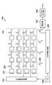
画素領域200には、後述するように、アバランシェフォトダイオードとカウンター回路とを有する単位画素201が行列状に配置されている。ここでは、説明を簡単にするために4×4画素の配列を示してあるが、実用上はさらに多数の画素が配置される。単位画素201は、入射したフォトンの数を計数してデジタルの信号値として出力することが可能である。なお、単位画素201の詳細は、図3を参照して説明する。
In the
垂直制御回路202は、画素領域200の画素をスイッチ205により1行単位で選択する。また、垂直制御回路202は、不図示の配線を介して画素領域の画素に行単位で制御信号を送出する。この制御信号の詳細についても、図3を参照して後述する。
The
水平制御回路203は、画素領域200の画素をスイッチ206により1列単位で選択する。垂直制御回路202と水平制御回路203の組み合わせにより選択された画素の画素信号は、補正部207に出力される。
The
補正部207は、各画素から出力された画素信号に対して単位時間当たりの受光量の違いによって生じる画質劣化を抑制するための補正処理(画像処理)を行う。また、補正部207では、画素信号の黒レベルを基準値に合わせる補正処理も行う。これらの補正処理の詳細は、図8を参照して後述する。
The
デジタル出力部208は、補正部207で補正処理(画像処理)された画素信号を、撮像素子100の外部に出力する。TG204は、各画素の画素信号を出力するための制御信号を、垂直制御回路202および水平制御回路203に送出する。なお、TG204は、不図示の配線を介して補正部207、デジタル出力部208にも制御信号を送出する。
The
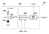
図3は、単位画素201の構成を示す図である。単位画素201は、大きく分けて、受光部301と計数部302を備える。
FIG. 3 is a diagram showing the configuration of the
受光部301は、フォトダイオード(PD)303、クエンチ抵抗304、反転バッファ305を含んで構成される。PD303は、アバランシェフォトダイオードであり、クエンチ抵抗304を介して降伏電圧より大きな逆バイアス電圧Vbiasが印加され、ガイガーモードで動作する。したがって、PD303にフォトンが入射するとアバランシェ増倍現象を引き起こし、アバランシェ電流が発生する。クエンチ抵抗304は、PD303のアバランシェ増倍現象を停止されるための抵抗素子である。反転バッファ305は、アバランシェ増倍現象によって生じた電圧変化をパルス信号(以下、「PLS信号」と記す。)として取り出すために設けられる。
The
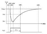
ここで、図4を参照して、受光部301の動作について説明する。図4は、PD303にフォトンが入射した際のカソード端子電圧Voutと、反転バッファ305から出力されるPLS信号の時間変化を表す図である。ここで、カソード端子電圧Voutは、PD303に印加される逆バイアス電圧の大きさでもある。
Here, the operation of the
時刻t401では、PD303には、降伏電圧Vbrより大きな逆バイアス電圧Vbiasが印加さており、ガイガーモードで動作している。この状態で時刻t402において、PD303にフォトンが入射すると、PD303で生成されたキャリアがアバランシェ増倍現象を引き起こし、アバランシェ電流が発生する。このアバランシェ電流により、クエンチ抵抗304に接続されたPD303のカソード端子電圧Voutが低下し始める。時刻t404でVoutが降伏電圧Vbrを下回るとアバランシェ増倍現象が停止する。そして、Vbiasを印加している電源からクエンチ抵抗304を介して再充電が行われるため、カソード端子電圧Voutは上昇し始める。時刻t406で再充電が完了すると、Voutは、再び逆バイアス電圧Vbiasに戻る。ここで、再充電に掛かる時間はクエンチ抵抗304の抵抗値と寄生容量に依存する。
At time t401, a reverse bias voltage Vbias larger than the breakdown voltage Vbr is applied to the
反転バッファから出力されるPLS信号がL→HおよびH→Lに切り替わる閾値をVthとすると、図4に示すように、時刻t403~t405の間でPLS信号はHとなる。したがって、1回のフォトン入射によって、1つのPLS信号が受光部301から出力される。ここで、時刻t403~t405で発生するPLS信号のパルス幅をΔTpと記す。
Assuming that the threshold value at which the PLS signal output from the inversion buffer switches from L to H and H to L is Vth, the PLS signal becomes H between the times t403 and t405 as shown in FIG. Therefore, one PLS signal is output from the
図3の説明に戻り、計数部302は、カウンター回路306、画素メモリ307を含んで構成される。カウンター回路306には、受光部301でフォトンの入射により発生したPLS信号が入力され、PLS信号がLからHに変化した回数をパルス数として計数する。また、カウンター回路306には、垂直制御回路202からイネーブル信号(以下、「PEN信号」と記す。)およびリセット信号(以下、「PRES信号」と記す。)が供給される。カウンター回路306に供給されるPEN信号がHレベルの状態で、PLS信号がLからHに変化すると、計数値が1つ増加する。PEN信号がLレベルの状態では、PLS信号がLからHに変化しても、計数値は増加せず、現在の計数値が保持される。また、カウンター回路306に供給されるPRES信号がHレベルになると、カウンター回路306の計数値は0にリセットされる。
Returning to the description of FIG. 3, the
画素メモリ307は、カウンター回路306で計数した計数値をデジタルの画素信号として取込み、その画素信号を補正部207に読み出している間、一時的に保持するためのメモリである。画素メモリ307には垂直制御回路202からラッチ信号(以下、「PLAT信号」と記す。)が供給される。PLAT信号がLからHに変化すると、画素メモリ307は、その時点でのカウンター回路306の計数値をデジタルの画素信号として取り込んで保持する。これ以降、カウンター回路306が計数している値を計数値、画素メモリ307が保持した値を画素信号と表記して区別する。
The
垂直制御回路202と水平制御回路203の組み合わせによって選択された画素の画素メモリ307に保持された画素信号は、補正部207に出力される。
The pixel signal held in the
なお、第1の実施形態においては、垂直制御回路202から供給されるPEN信号、PRES信号およびPLAT信号は、画素領域200内のすべての画素で同時に制御されるものとして説明するが、行単位で制御するタイミングを切り替えてもよい。
In the first embodiment, the PEN signal, the PRES signal, and the PLAT signal supplied from the
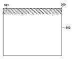
また、画素領域200の一部領域は、図5に示すようにオプティカルブラック画素領域(以下、「OB領域」と記す。)501と開口画素領域502で構成される。OB領域501に配置される画素(OB画素)の受光部301は不図示の金属遮光層等で遮光され、PD303に光が入射しない構成になっている。OB領域の各画素から出力された画素信号は、補正部207で画素信号の黒レベルを基準値に合わせる補正に用いられる。一方、開口画素領域502に配置される画素の受光部301は、PD303に光が入射するように不図示の開口を備える。開口画素領域の各画素からは、受光量に応じた画素信号が出力される。
Further, a part of the
なお、図5では、OB領域501を画素領域の上側一帯に配置してあるが、例えば、画素領域200の左側や右側等、配置箇所は適宜選択することができる。
In FIG. 5, the
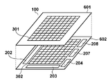
図6に、撮像素子100のチップレイアウトの一例を示す。撮像素子100は、受光部基板601、計数部基板602を積層させた構成を有する。各基板間の配線は、シリコン貫通電極等を用いて電気的に接続される。受光部基板601には、各画素の受光部301が行列状に配置される。計数部基板602には、各画素の計数部302が行列状に配置される。また、計数部基板602には、垂直制御回路202および水平制御回路203、TG204、補正部207、デジタル出力部208も配置される。図5に示すように、受光部301と計数部302とを別々の基板に形成することで、受光部301の面積を確保することができ、これにより、受光部の開口率の低下を防止することができる。なお、撮像素子100を積層構造にせず、同一の基板上に形成してもよい。
FIG. 6 shows an example of the chip layout of the
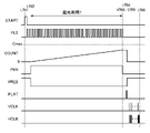
図7は、第1の実施形態において、1フレームの画像を取得する際の撮像装置の駆動タイミングチャートを示す。時刻t701で撮影開始信号STARTがL→H→Lになると、各画素の受光部301にバイアス電圧Vbiasが供給される。そして、PD303には、降伏電圧より大きな逆バイアス電圧が印加され、ガイガーモードで動作を開始する。これにより、受光部301からは、入射したフォトンの数に応じてPLS信号が出力される。COUNTは任意の画素のカウンター回路306が計数した計数値の一例を示す。Cmaxは、カウンター回路306で計数できる最大値である。
FIG. 7 shows a drive timing chart of an image pickup apparatus when acquiring an image of one frame in the first embodiment. When the shooting start signal START changes from L to H to L at time t701, the bias voltage Vbias is supplied to the
時刻t701の時点では、PRES信号はHになっており、各画素のカウンター回路306の計数値は0にリセットされている。
At the time t701, the PRES signal is H, and the count value of the
時刻t702で、PRES信号がLとなり、各画素のカウンター回路306のリセットが解除される。同時にPEN信号がHとなり、各画素のカウンター回路306はイネーブル状態となる。したがって、各画素のカウンター回路306では、入力されたPLS信号に応じて計数値が増加する。これにより撮像装置の露光期間が開始する。この露光期間は時刻t703でPEN信号がLになるまで続く。この時刻t702からt703までの露光期間の長さをTとする。
At time t702, the PRESS signal becomes L, and the reset of the
時刻t703で露光期間Tが終了すると、PEN信号がLになる。これにより、各画素のカウンター回路306がディセーブル状態になり、カウンター回路306にPLS信号が入力されても計数値が増加しなくなる。また、受光部301へのバイアス電圧Vbiasの供給が停止し、受光部301はPLS信号を出力しなくなる。そして時刻t704で垂直制御回路202から各画素に対して供給しているPLAT信号が一斉にL→Hに変化する。これにより各画素のカウンター回路306の計数値が画素信号として画素メモリ307に保持される。その後、PLAT信号はLに戻る。また、画素メモリ307に画素信号が保持されると、すぐにPRES信号がHになり、各画素のカウンター回路306の計数値が0にリセットされる。
When the exposure period T ends at time t703, the PEN signal becomes L. As a result, the
時刻t705~t706では、垂直制御回路202にTG204からVCLK信号が供給される。VCLK信号がHになる毎に、各行のスイッチ205が順番にオンし、垂直制御回路202が画素領域200の画素を1行ずつ選択していく。そして、任意の1行が選択されると、水平制御回路203にTG204からHCLK信号が供給され、各列のスイッチ206が順番にオンする。これにより、選択行の画素の画素メモリ307に保持されていた画素信号が補正部207に順次出力される。
At times t705 to t706, a VCLK signal is supplied from the
その後、補正部207で補正処理された画素信号は、デジタル出力部208を介して撮像素子100の外部に順次出力される。
After that, the pixel signal corrected by the
図8に、補正部207の構成を示す。補正部207は、カウントレート算出部801、ゲイン補正部802、黒レベル補正部803を含んで構成される。カウントレート算出部801およびゲイン補正部802は、単位時間あたりの受光量の違いによって生じる画質劣化を補正する。黒レベル補正部803は、各画素のPD303で発生した暗電流に起因して受光部301から出力されるPLS信号をカウンター回路306で計数して増加してしまった画素信号成分(暗電流成分)を、オフセット補正により除去する。
FIG. 8 shows the configuration of the
ここで、図9および図10を用いて、単位時間あたりの受光量の違いによって生じる画質劣化(誤差)の補正方法について説明する。 Here, with reference to FIGS. 9 and 10, a method for correcting image quality deterioration (error) caused by a difference in the amount of light received per unit time will be described.
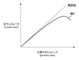
図9に、任意の画素の入射フォトンレートと、カウンター回路306のカウントレートとの関係を示す。ここで、入射フォトンレートは受光部301に単位時間あたりに入射するフォトンの数であり、単位時間あたりの受光量に比例した値となる。カウントレートはカウンター回路306の計数値の単位時間あたりの増加量である。本来であれば、理想値で示すようにカウントレートと入射フォトンレートは比例する。しかし、入射フォトンレートが高い状態、つまり単位時間あたりの受光量が多い状態では、1つのフォトンが入射して発生したPLS信号がH→Lに戻る前に新たなフォトンが入射してしまう。その結果、複数のPLS信号が重なってしまうため、カウンター回路306で計数する計数値が、本来のフォトンの数よりも低下してしまう。したがって、図9の901に示すように、入射フォトンレートが高くなるほど、カウントレートが本来の値よりも低下してしまう。
FIG. 9 shows the relationship between the incident photon rate of an arbitrary pixel and the count rate of the
図10に、カウントレートに対する入射フォトンレートの関係を示す。この図10は、図9のグラフの縦軸と横軸を入れ替えたものである。図10に示すように、各画素のカウントレートに応じて、矢印1001のように理想値となるように画素信号にゲイン補正をすることで、受光量に対して線形な画素信号を得ることができる。ここで、入射フォトンレートがPmax以上となる斜線で示す領域では、入射フォトンレートが増えるにつれてカウントレートが減少し始める。したがって、入射フォトンレートがPmax以上となる場合は、カウントレートから本来の入射フォトンレートを算出することができない。そのため、撮影前に測光部109で測光処理を行い、その測光結果から、入射フォトンレートがPmax以上となるような高輝度被写体を含むと全体制御・演算部が判定した場合は、入射フォトンレートがPmax未満になるように撮影レンズの絞り制御を行ってから撮影すればよい。または、特許文献1に記載のように、各画素に受光部から出力されたPLS信号のパルス幅を累積加算する累積手段を設け、受光量に対して単調増加する信号が各画素から出力されるようにしてもよい。
FIG. 10 shows the relationship between the incident photon rate and the count rate. In FIG. 10, the vertical axis and the horizontal axis of the graph of FIG. 9 are interchanged. As shown in FIG. 10, it is possible to obtain a pixel signal linear with respect to the amount of received light by performing gain correction on the pixel signal so as to have an ideal value as shown by
次に、図8の各ブロックの具体的な処理について説明する。カウントレート算出部801には、各画素から出力された画素信号が順次入力される。そして、画素信号を露光期間Tで除算することで、単位時間あたりのカウント値の増加量であるカウントレートを算出する。
Next, the specific processing of each block of FIG. 8 will be described. Pixel signals output from each pixel are sequentially input to the count
ゲイン補正部802は、カウントレート算出部801で算出したカウントレートをもとに、対応する画素の画素信号にゲイン補正を行う。各画素から出力され補正部207に入力される画素信号をx、ゲイン補正後の画素信号をyとすると、ゲイン補正後の画素信号yは、式(1)により表すことができる。
y = α(r) × x …(1)
The
y = α (r) × x… (1)
ここで、α(r)はゲイン補正係数、rはカウントレート算出部801で算出したカウントレートである。
図11にゲイン補正係数α(r)の例を示す。同図に示すように、ゲイン補正係数α(r)は、カウントレート算出部801で算出したカウントレートrによって異なる値をとる。このゲイン補正係数α(r)は図10のカウントレートが理想値になるために必要なゲイン補正量である。
Here, α (r) is a gain correction coefficient, and r is a count rate calculated by the count
FIG. 11 shows an example of the gain correction coefficient α (r). As shown in the figure, the gain correction coefficient α (r) takes a different value depending on the count rate r calculated by the count
ゲイン補正係数α(r)は、ゲイン補正部802においてカウントレートrに応じた補正テーブルとして記憶しておけばよい。または、カウントレートrの近似関数として記憶しておき、各画素のカウントレートに応じてゲイン補正係数α(r)を算出してもよい。
The gain correction coefficient α (r) may be stored in the
黒レベル補正部803は、ゲイン補正部802でゲイン補正された画素信号が入力され、オフセット補正により画素信号から暗電流成分を除去する。具体的には、OB領域501の画素信号を積算し、その平均値を算出することで、暗電流成分を算出する。そして、その平均値を開口画素領域502の各画素の画素信号から減算することで、暗電流成分を除去する。
The black
黒レベル補正部803で補正された画素信号は、順次デジタル出力部208に送出され、撮像素子100の外部に出力される。
The pixel signals corrected by the black
なお、ゲイン補正部802によるゲイン補正は、黒レベル補正部803によるオフセット補正よりも前で行っている。これは、受光部301において暗電流によって発生したパルス信号とフォトンの入射によって発生したパルス信号が重なることで、カウンター回路306で計数したフォトンによる画素信号成分と暗電流成分の双方が本来の値よりも低下するためである。したがって、ゲイン補正部802において、本来のフォトンによる画素信号成分および暗電流成分になるようにゲイン補正を行った後、黒レベル補正部803で画素信号からOB領域の平均画素信号を減算することで、暗電流成分を好適に除去することができる。
The gain correction by the
なお、フォトンによる画素信号成分に比べて暗電流成分が十分小さい場合には、黒レベル補正部803でオフセット補正を行った後、ゲイン補正部802でゲイン補正を行う構成にしてもよい。
If the dark current component is sufficiently smaller than the pixel signal component due to photons, the black
以上で述べた補正部207の補正処理により単位時間あたりの受光量の違いによって生じる画質劣化を抑制することができる。なお、補正部207で行う補正処理は、信号処理部101や全体制御・演算部104で行う構成にしてもよい。
By the correction process of the
<変形例>
図3に示した単位画素201では、クエンチ抵抗304を用いてアバランシェ増倍を停止させていたが、クエンチ抵抗として、MOSトランジスタの抵抗成分を利用してもよい。図12に、第1の実施形態の変形例による単位画素201の構成を示す。図12は、図3に示す単位画素の構成に対応し、図3と同一の箇所については同一の番号を付与し、その説明は省略する。
<Modification example>
In the
図12は、MOSトランジスタ1201のドレイン-ソース間の抵抗成分をクエンチ抵抗として利用した場合の構成を示している。本構成では、MOSトランジスタ1201のゲート電圧Vqncを変えることで、ドレイン-ソース間の抵抗値を変化させ、図4の時刻t404~406で示す再充電にかかる時間を変化させることができる。例えば、ゲート電圧Vqncをゲート閾値電圧以上にすることでMOSトランジスタ1201をオンさせると、ドレイン-ソース間の抵抗値が減少する。これにより再充電にかかる時間が短縮し、PLS信号のパルス幅ΔTpが短縮される。したがって、複数のフォトンが連続して受光部に入射した際に、それぞれのフォトンにより発生したパルスが重なってしまう確立を減少させることができる。
FIG. 12 shows a configuration when the resistance component between the drain and the source of the
その結果、図9で示した入射フォトンレートが高い場合の出力カウントレートの低下を減少させることができる。この場合、ゲイン補正部802で画素信号に乗算するゲイン補正係数α(r)をパルス幅ΔTpに応じて変えることで過補正になることを抑えることができる。したがって、単位時間あたりの受光量の違いによって生じる画質劣化を好適に抑制することが可能となる。
As a result, it is possible to reduce the decrease in the output count rate when the incident photon rate shown in FIG. 9 is high. In this case, overcorrection can be suppressed by changing the gain correction coefficient α (r) to be multiplied by the pixel signal by the
<第2の実施形態>
次に、本発明の第2の実施形態について説明する。上述した第1の実施形態では、画素毎にカウントレートを算出して、カウントレートに応じたゲイン補正係数を用いて補正を行っていた。これに対し、第2の実施形態では、測光部109の測光結果に基づいて画素信号に応じたゲイン補正係数を選択する。
<Second embodiment>
Next, a second embodiment of the present invention will be described. In the first embodiment described above, the count rate is calculated for each pixel, and the gain correction coefficient corresponding to the count rate is used for correction. On the other hand, in the second embodiment, the gain correction coefficient corresponding to the pixel signal is selected based on the photometric result of the
図13は、第2の実施形態における補正部207の構成を示すブロック図であり、第1の実施形態で説明した図8に示す補正部207に代えて用いられる。なお、図8と同様の構成については同じ参照番号を付し、説明を省略する。また、補正部207以外の構成は上述した第1の実施形態と同様であるため、説明を省略する。
FIG. 13 is a block diagram showing the configuration of the
補正係数選択部1301は、測光部109で行った測光の測光結果を取得し、その結果に応じて、画素信号に応じたゲイン補正係数を選択する。具体的には、測光部109の測光エリア毎に測定した被写体輝度のうち、最大の輝度値に応じて図14のγ1(x)~γ3(x)で示すゲイン補正係数のいずれかを選択する。ここで、xはゲイン補正部1302に入力される画素信号であり、γ1(x)~γ3(x)は画素信号に応じたゲイン補正係数である。
The correction
測光部109で測定した最大輝度値が予め決められた第1の閾値よりも低い場合はゲイン補正係数γ1(x)が選択され、最大輝度値が予め決められた第2の閾値以上の場合には、ゲイン補正係数γ3(x)が選択される。なお、第1の閾値<第2の閾値である。また、両者の中間の場合は、ゲイン補正係数γ2(x)が選択される。すなわち、同じ画素信号であっても、測光部109で測定した最大輝度値が高いほど、ゲイン補正量が大きくなるようなゲイン補正係数が選択される。これは、最大輝度値が高いほど、撮影時の単位時間あたりの受光量が増え、受光部からのパルス信号が重なることで発生する画素信号の低下の影響が大きくなるためである。
When the maximum luminance value measured by the
ゲイン補正部1302では、補正係数選択部1301で選択した補正係数を以下の式(2)のように画素信号xに乗算する。
y = γ(x) × x …(2)
The
y = γ (x) × x… (2)
ここで、yはゲイン補正後の画素信号、γ(x)は、補正係数選択部1301により、測光結果及び画素信号に基づいて選択されたゲイン補正係数である。
ゲイン補正部1302でゲイン補正された画素信号は、第1の実施形態と同様に、黒レベル補正部803でオフセット補正が行われ、補正後の画素信号がデジタル出力部に出力される。
Here, y is the gain-corrected pixel signal, and γ (x) is the gain correction coefficient selected by the correction
The pixel signal gain-corrected by the
図15に、第2の実施形態における自動露出撮影処理のフローチャートを示す。撮影が開始されると、まずS1501において、測光部109において測光処理を行う。具体的には、測光部109の測光エリア毎に被写体輝度を測定する。
FIG. 15 shows a flowchart of the automatic exposure shooting process according to the second embodiment. When shooting is started, first, in S1501, the
次にS1502において、測光部109の測光結果に応じて全体制御・演算部104が、絞り、露光期間等の撮影条件を設定する。S1503では、補正係数選択部1301で、ゲイン補正係数の選択が行われる。ここでは、図14を参照して上述したように、測光部109で測定した最大輝度値が高いほど、ゲイン補正量が大きくなるようなゲイン補正係数が選択される。
Next, in S1502, the overall control /
S1504では、S1502で設定した撮影条件で撮像素子100により撮影を行う。具体的には、図7に示す駆動を行い、画素領域200から画素信号が補正部207に順次出力される。
In S1504, image pickup is performed by the
S1505では、画素領域200から順次出力される画素信号に対して補正部207にて補正処理を行う。ゲイン補正部1302では、補正係数選択部1301で選択されたゲイン補正係数のうち、画素信号に応じて選択されたゲイン補正係数を画素信号に乗算する。これにより、受光部からのパルス信号が重なることで発生する画素信号の低下を補うことができる。その後、黒レベル補正部803でオフセット補正された画素信号が撮像素子100から出力され、そして、S1506で、記録部107にて画像データとして保存される。
In S1505, the
以上で述べた補正部207の補正処理により単位時間あたりの受光量の違いによって生じる画質劣化を抑制することができる。
By the correction process of the
<第3の実施形態>
次に、本発明の第3の実施形態について説明する。第3の実施形態では、単位時間あたりの受光量に応じて、黒レベル補正部の補正量を変える構成について説明する。
<Third embodiment>
Next, a third embodiment of the present invention will be described. In the third embodiment, a configuration in which the correction amount of the black level correction unit is changed according to the amount of light received per unit time will be described.
単位時間あたりの受光量が大きい画素では、頻繁にアバランシェ増倍現象が発生し、大電流がクエンチ抵抗304を流れるため、クエンチ抵抗304での発熱量が大きくなる。そのため、クエンチ抵抗304の付近にあるPD303の温度が上昇し、暗電流量が増加する。その結果、光が入射しないOB領域の画素(OB画素)と、単位時間あたりの受光量の多い画素とで暗電流量に差が生じてしまう。そこで、第3の実施形態では、単位時間当たりの受光量に応じて黒レベル補正部の補正量を変更する。
In a pixel having a large amount of light received per unit time, the avalanche multiplication phenomenon frequently occurs and a large current flows through the quench
図16に、第3の実施形態における補正部207の構成を示すブロック図であり、第1の実施形態で説明した図8に示す補正部207に代えて用いられる。なお、図8と同様の構成については同じ参照番号を付し、説明を省略する。また、補正部207以外の構成は上述した第1の実施形態と同様であるため、説明を省略する。
FIG. 16 is a block diagram showing the configuration of the
空間フィルタ処理部1601は、カウントレート算出部801で算出した画素毎のカウントレートに対してフィルタ処理を行う。例えば、対象画素とその周囲8画素のカウントレートの平均値である平均カウントレートを計算する。なお、フィルタ処理として、重み付け平均処理を行ってもよい。
The spatial
なお、対象画素よりも後に読み出す画素のカウントレートを平均化の対象とする場合は、補正部207の前に不図示の保持メモリを設けて、画素信号を一時的に保持してから空間フィルタ処理部1601でフィルタ処理を行うようにすればよい。黒レベル補正部1602には、ゲイン補正部802から出力された画素信号が入力され、以下の式(3)のようにオフセット補正を行う。
z = y - β(rave) × drk …(3)
When the count rate of pixels read after the target pixel is targeted for averaging, a holding memory (not shown) is provided in front of the
z = y - β (rave) × drk … (3)
ここで、zはオフセット補正後の画素信号、yは黒レベル補正部1602に入力される画素信号、drkはOB領域の平均画素信号、raveは空間フィルタ処理部1601で算出した平均カウントレートである。β(rave)はオフセット補正係数であり、平均カウントレートraveに応じた値となる。
ここで、オフセット補正係数β(rave)の詳細について、図17を参照して説明する。図17(a)は、画素領域の任意の一列の画素のカウントレートを算出した例を示す。1701に示すように単位時間あたりの受光量が多い画素では、カウントレートが高くなる。また、実線で示す温度のようにカウントレートの高い画素付近では、アバランシェ電流による発熱によって温度が高くなる。破線で示す平均カウントレートは空間フィルタ処理部1601で各画素のカウントレートを平均化処理した値である。
Here, z is the pixel signal after offset correction, y is the pixel signal input to the black
Here, the details of the offset correction coefficient β ( rave ) will be described with reference to FIG. FIG. 17A shows an example of calculating the count rate of a pixel in an arbitrary row in the pixel area. As shown in 1701, a pixel having a large amount of light received per unit time has a high count rate. Further, in the vicinity of a pixel having a high count rate such as the temperature shown by the solid line, the temperature rises due to heat generated by the avalanche current. The average count rate shown by the broken line is a value obtained by averaging the count rates of each pixel by the spatial
図17(b)は、図17(a)に対応する画素の暗電流量の例である。1702に示す位置の付近の画素では、温度が高いため、OB領域に比べて暗電流量が多くなる。実線で示すβ(rave)はOB領域の平均画素信号に乗算するオフセット補正係数である。オフセット補正係数β(rave)は、図17(b)に示すように、図17(a)の平均カウントレートが高い画素ほど大きな値となる。これにより、OB領域と、単位時間あたりの受光量が多い画素とで暗電流量が異なっていても、画素信号から暗電流成分を好適に除去することができる。 FIG. 17B is an example of the amount of dark current of the pixel corresponding to FIG. 17A. Since the temperature of the pixels near the position shown in 1702 is high, the amount of dark current is larger than that in the OB region. Β ( rave ) shown by the solid line is an offset correction coefficient to be multiplied by the average pixel signal in the OB region. As shown in FIG. 17 (b), the offset correction coefficient β ( rave ) becomes a larger value as the average count rate in FIG. 17 (a) is higher. As a result, even if the amount of dark current differs between the OB region and the pixel having a large amount of light received per unit time, the dark current component can be suitably removed from the pixel signal.
なお、空間フィルタ処理部1601のフィルタ処理は、画素領域200がベイヤー配列のカラーフィルターを備えている場合は、同一色の画素のみで平均化処理を行う構成にしてもよい。また、空間フィルタ処理部1601を設けず、カウントレート算出部801で算出したカウントレートに応じたオフセット補正係数を用いてもよい。
When the
上記の通り第3の実施形態によれば、単位時間あたりの受光量が多い画素の画素信号から暗電流成分を好適に除去することができ、単位時間あたりの受光量の違いによって生じる画質劣化を抑制することができる。 As described above, according to the third embodiment, the dark current component can be suitably removed from the pixel signal of the pixel having a large amount of light received per unit time, and the image quality deterioration caused by the difference in the amount of light received per unit time can be prevented. It can be suppressed.
<第4の実施形態>
次に、本発明の第4の実施形態について説明する。動画等で連続して撮影を行う場合、高輝度の被写体が移動すると、被写体のあった位置の画素のカウントレートは低下するが、温度はそれよりもゆるやかに変化する。そして、各画素の暗電流量も温度変化に従ってゆるやかに変化する。このような場合でも暗電流成分を好適に補正することができる構成について説明する。
<Fourth Embodiment>
Next, a fourth embodiment of the present invention will be described. When shooting a moving image continuously, when a high-brightness subject moves, the count rate of the pixels at the position where the subject is located decreases, but the temperature changes more slowly. Then, the amount of dark current of each pixel also changes slowly according to the temperature change. A configuration in which the dark current component can be suitably corrected even in such a case will be described.
図18は、第4の実施形態における補正部207の構成を示すブロック図であり、第1の実施形態で説明した図8に示す補正部207に代えて用いられる。なお、図8と同様の構成については同じ参照番号を付し、説明を省略する。また、補正部207以外の構成は上述した第1の実施形態と同様であるため、説明を省略する。
FIG. 18 is a block diagram showing the configuration of the
時間フィルタ処理部1801はカウントレート算出部801で算出したカウントレートを複数フレームにわたってフィルタ処理をする。例えば、現在のフレームとそれより前の4フレーム分の画素毎の平均カウントレートを算出する。また、時間フィルタ処理部1801は、各画素の平均カウントレートを保持するための不図示の保持メモリを備える。
The time
黒レベル補正部1802にはゲイン補正部802から出力された画素信号が入力され、時間フィルタ処理部1801で算出した平均カウントレートに応じてオフセット補正係数βを用いて黒レベルの補正を行う。この補正方法は第3の実施形態において説明した式(3)と同様であるため、説明を省略する。
The pixel signal output from the
図19(a)に画素領域の任意の一つの画素のカウントレートを撮影フレーム毎に算出した例を示す。1901のフレームに示すように高輝度被写体の移動等により対象画素のカウントレートが低下した場合でも、同図に実線で示す対象画素の温度はすぐには低下せず、ゆるやかに追従する。そのため、図19(b)に示すように、各撮影フレームの暗電流は温度に従ってゆるやかに変化する。また、破線で示す平均カウントレートは時間フィルタ処理部1801で対象画素のカウントレートを複数フレームにわたって平均化処理した値である。
FIG. 19A shows an example in which the count rate of any one pixel in the pixel area is calculated for each shooting frame. Even when the count rate of the target pixel decreases due to the movement of a high-luminance subject as shown in the frame of 1901, the temperature of the target pixel shown by the solid line in the figure does not decrease immediately and follows slowly. Therefore, as shown in FIG. 19B, the dark current of each photographing frame changes slowly according to the temperature. The average count rate shown by the broken line is a value obtained by averaging the count rates of the target pixels over a plurality of frames by the time
図19(b)は、図19(a)に対応するフレームの暗電流量の例である。1902に示すフレームでは、カウントレートは低下しているが、画素の温度がまだ高いため、カウントレートと比べて暗電流量は多いままである。実線で示すβ(rave)は式(3)でOB領域の平均画素信号に乗算するオフセット補正係数である。オフセット補正係数β(rave)は、図17(a)の平均カウントレートが高い画素ほど大きな値となる。このオフセット補正係数をOB領域の平均画素信号に乗算した値を用いてオフセット補正することで、画素信号から暗電流成分を除去することができる。 FIG. 19B is an example of the amount of dark current of the frame corresponding to FIG. 19A. In the frame shown in 1902, the count rate is reduced, but the dark current amount remains higher than the count rate because the pixel temperature is still high. Β ( rave ) shown by the solid line is an offset correction coefficient to be multiplied by the average pixel signal in the OB region in the equation (3). The offset correction coefficient β ( rave ) becomes a larger value as the average count rate in FIG. 17 (a) is higher. By performing offset correction using the value obtained by multiplying the average pixel signal in the OB region by this offset correction coefficient, the dark current component can be removed from the pixel signal.
上記の通り第4の実施形態によれば、動画撮影等の最中に単位時間あたりの受光量が大きく変化した場合でも、画素信号から暗電流成分を好適に除去することができる。 As described above, according to the fourth embodiment, the dark current component can be suitably removed from the pixel signal even when the light receiving amount per unit time changes significantly during moving image shooting or the like.
<第5の実施形態>
次に、本発明の第5の実施形態について説明する。上述した第1の実施形態では、露光期間終了後に出力した画素信号をもとにカウントレートを算出し、補正を行っていたため、露光期間中に被写体輝度が変化した場合に正確なカウントレートを求めることができなかった。これに対し、第5の実施形態では、露光期間中に被写体輝度が変化した場合でも対応可能な構成について説明する。
<Fifth Embodiment>
Next, a fifth embodiment of the present invention will be described. In the first embodiment described above, the count rate is calculated and corrected based on the pixel signal output after the end of the exposure period, so that an accurate count rate is obtained when the subject brightness changes during the exposure period. I couldn't. On the other hand, in the fifth embodiment, a configuration that can cope with a change in subject brightness during the exposure period will be described.
図20に、第5の実施形態における撮像素子100’の全体構成を示す図であり、第1の実施形態で説明した図2に示す撮像素子100に代えて用いられる。なお、図2と同様の構成については同じ参照番号を付し、説明を省略する。また、撮像素子100’以外の構成は上述した第1の実施形態と同様であるため、説明を省略する。
FIG. 20 is a diagram showing the overall configuration of the image pickup device 100'in the fifth embodiment, and is used in place of the
信号処理ブロック2000は、補正部207と、フレームメモリ2001と、加算部2002とを備える。フレームメモリ2001は、一時メモリ領域2001aと積算メモリ領域2001bとを備え、露光期間中に各画素からデジタルの画素信号を取得して、保持する記憶回路である。一時メモリ領域2001aは、各画素からデジタルの画素信号を取得し、一時的に保持する。一時メモリ領域2001aに保持された画素信号は補正部207に入力され、第1の実施形態と同様の補正処理が行われる。
The
加算部2002は、積算メモリ領域2001bに保持されていた画像信号に、各画素から新たに読み出して補正処理された画像信号を同一アドレス毎に加算する。加算された画像信号は積算メモリ領域2001bに再び保持される。これにより、積算メモリ領域2001bは、露光期間中に補正部207で補正処理された画素信号を同一アドレス毎に積算された画素信号を保持する。ここで、一時メモリ領域2001aは、1画素あたり単位画素201から出力されるデジタルの画素信号と同一のビット幅を備える。一方、積算メモリ領域2001bは、単位画素201から出力されるデジタルの画素信号に比べて、十分大きなビット幅を備える。
The
積算メモリ領域2001bに保持された画素信号は、露光期間終了後にデジタル出力部208を介して撮像素子100の外部に出力される。なお、フレームメモリ2001および加算部2002、補正部207は、撮像素子100’の外部に設ける構成でもよい。
The pixel signal held in the
図21に、第5の実施形態における撮像素子100’のチップレイアウトの一例を示す。図21は、第1の実施形態の図6に対応し、図6と同一の構成については同一の番号を付与し、その説明は省略する。 FIG. 21 shows an example of the chip layout of the image pickup device 100'in the fifth embodiment. FIG. 21 corresponds to FIG. 6 of the first embodiment, and the same number is assigned to the same configuration as that of FIG. 6, and the description thereof will be omitted.
撮像素子100’は、受光部基板601、計数部基板602およびフレームメモリ基板2101を積層させた構成を有する。各基板間の配線は、シリコン貫通電極等を用いて電気的に接続される。フレームメモリ基板2101には、フレームメモリ2001および加算部2002、補正部207、デジタル出力部208が配置される。フレームメモリ基板2101を、受光部基板601および計数部基板602よりも微細なプロセスで製造すれば、フレームメモリ2001は、大きなビット数を確保できる。なお、撮像素子100’を積層構造にせず、同一の基板上に形成してもよい。
The image pickup device 100'has a configuration in which a light receiving
図22は、第5の実施形態において、1フレームの画像を取得する際の撮像装置の駆動タイミングチャートを示す。図22は、第1の実施形態の図7に示すタイミングチャートに対応し、図7と同一の動作をする処理については同一の番号を付与し、その説明は適宜省略する。 FIG. 22 shows a drive timing chart of the image pickup apparatus when acquiring an image of one frame in the fifth embodiment. FIG. 22 corresponds to the timing chart shown in FIG. 7 of the first embodiment, and the same numbers are assigned to the processes that perform the same operations as those of FIG. 7, and the description thereof will be omitted as appropriate.
図22では、t702からt703の露光期間Tを4つの露光期間(以下、「分割露光期間」と呼ぶ。)T1~T4に分割し、分割露光期間毎に各画素から画素信号をフレームメモリ2001へ読み出す。
In FIG. 22, the exposure period T from t702 to t703 is divided into four exposure periods (hereinafter, referred to as “divided exposure period”) T1 to T4, and a pixel signal is transmitted from each pixel to the
時刻t2201で分割露光期間T1が経過すると、垂直制御回路202からすべての画素に対して供給しているPLAT信号が一斉にL→H→Lと変化する。これにより、分割露光期間T1の間に各画素のカウンター回路306で計数していた計数値が、画素信号として、各画素の画素メモリ307に保持される。画素信号が画素メモリ307に保持されると、すぐにPRESがHになり、各画素のカウンター回路306の計数値が0にリセットされる。そして、PRESがLに戻ると、リセットが解除され、各画素のカウンター回路306は、再び入射したフォトンに応じて計数を開始する。
When the divided exposure period T1 elapses at the time t2201, the PLAT signals supplied to all the pixels from the
時刻t2202~t2203では、TG204から垂直制御回路202および水平制御回路203にそれぞれVCLK信号およびHCLK信号が供給される。そして、垂直制御回路202および水平制御回路203によって選択された画素の画素メモリ307に保持されていた画素信号が順次フレームメモリ2001内の一時メモリ領域2001aに保持される。一時メモリ領域2001aに保持された画素信号は、補正部207においてゲイン補正およびオフセット補正が行われ、補正後の画素信号は再び一時メモリ領域2001aに保持される。なお、ここで補正部207ににより行われる補正処理は、第1~第4の実施形態と同様のため、説明を省略する。
At times t2202 to t2203, the VCLK signal and the HCLK signal are supplied from the
そして、加算部2002において、一時メモリ領域2001aに保持された補正後の画素信号と、積算メモリ領域2001bに保持されていた同一アドレスの画素信号とを加算処理し、加算された画素信号を積算メモリ領域2001bに再び格納する。なお、上記補正処理および加算処理は、各画素の画素メモリ307内の画素信号をフレームメモリ2001に保持する動作と並行して行われる。
Then, in the
時刻t2202~t2204で行う最初の加算処理では、フレームメモリ2001内の積算メモリ領域2001bには、画素信号が保持されていないため、補正部207で補正処理された画素信号が、そのまま積算メモリ領域2001bに保持される。
In the first addition process performed at times t2202 to t2204, the pixel signal is not held in the
時刻t2204で分割露光期間T2が経過すると、再びPLAT信号がL→H→Lとなり、時刻t2201~t2203の時と同様に、各画素の画素信号がフレームメモリ2001の一時メモリ領域2001aに保持され、補正処理および加算処理が行われる。そして、加算処理が終わった画素信号は積算メモリ領域2001bに再び保持される。以降、分割露光期間毎に同様の処理が繰り返される。
When the divided exposure period T2 elapses at the time t2204, the PLAT signal changes from L to H to L again, and the pixel signal of each pixel is held in the
ここで、時刻t2201~t2203で行われる、各画素の画素メモリ307に保持された画素信号に対する、一時メモリ領域2001aへの保持および補正部207の補正処理、加算部2002の加算処理は、時刻t2204までに完了している必要がある。すなわち、次の分割露光期間が経過する前に完了している必要がある。したがって、この時間内に処理が完了するような動作周波数を設定する。または、次の分割露光期間が経過する前に処理が完了するように、分割露光期間の長さや分割数を調節する。
Here, the pixel signal held in the
時刻t703で、1フレーム分の露光期間Tが終了すると、PEN信号がLとなる。これにより、各画素のカウンター回路306がディセーブル状態になり、カウンター回路306の計数値が増加しなくなる。また、受光部301へのバイアス電圧Vbiasの供給が停止し、受光部301はPLS信号を出力しなくなる。そして、時刻t2206で、PLAT信号がL→H→Lと切り替わり、露光終了時にカウンター回路306で計数していた計数値が画素メモリ307に保持される。そして、PRES信号がHになり、カウンター回路306の計数値が0にリセットされる。
At time t703, when the exposure period T for one frame ends, the PEN signal becomes L. As a result, the
その後、時刻t2207~t2208では、t2202~t2203の時と同様に、各画素の画素信号が一時メモリ領域2001aに保持される。そして、補正処理および加算処理された画素信号が、積算メモリ領域2001bに保持される。このとき、積算メモリ領域2001bに保持された画素信号は、時刻t702~t703の露光期間中に画素メモリ307から取得した画素信号を積算した信号となる。この画素信号は、露光期間中に入射したフォトンの数に応じた信号となる。
After that, at times t2207 to t2208, the pixel signal of each pixel is held in the
上記の通り本第5の実施形態によれば、分割した露光期間毎にカウントレートを算出して補正する。これにより、第1の実施形態と比べて、露光期間中に被写体輝度が変化した場合でも単位時間あたりの受光量の違いによって生じる画質劣化を好適に抑制することが可能となる。なお、上述した第5の実施形態における露光期間を分割する数や分割露光期間の長さは一例であり、本発明はこれに限られるものではない。 As described above, according to the fifth embodiment, the count rate is calculated and corrected for each divided exposure period. This makes it possible to suitably suppress image quality deterioration caused by a difference in the amount of light received per unit time even when the subject brightness changes during the exposure period, as compared with the first embodiment. The number of divided exposure periods and the length of the divided exposure period in the fifth embodiment described above are examples, and the present invention is not limited thereto.
<第6の実施形態>
次に、本発明の第6の実施形態について説明する。上述した第5の実施形態では、露光期間中に画素信号をフレームメモリ2001に読み出す度にカウンター回路の計数値をリセットしたが、本第6の実施形態では、露光期間中にカウンター回路の計数値をリセットしない構成について説明する。なお、第6の実施形態では、第5の実施形態と同様に、露光期間中に被写体輝度が変化した場合でも対応可能な構成である。
<Sixth Embodiment>
Next, a sixth embodiment of the present invention will be described. In the fifth embodiment described above, the count value of the counter circuit is reset every time the pixel signal is read into the
図23は、画素領域200から出力された画素信号に信号処理をする信号処理ブロック2300の構成を示す。信号処理ブロック2300は、第5の実施形態において図20に示した信号処理ブロック2000の代わりに用いられる。なお、これ以外の箇所については、第5の実施形態と同様であるため、説明を省略する。
FIG. 23 shows the configuration of the
フレームメモリ2301は、露光期間中に各画素からデジタルの画素信号を取得して、保持する記憶回路であり、一時メモリ領域A2311、一時メモリ領域B2312、積算メモリ領域2313で構成される。一時メモリ領域A2311および一時メモリ領域B2312は、各画素からデジタルの画素信号を取得し、一時的に保持するための一時メモリである。露光期間中に各画素から読み出し動作を行う毎に、読み出された画素信号は一時メモリ領域A2311と一時メモリ領域B2312に交互に保持される。積算メモリ領域2313は、露光期間中に補正部207で補正処理された画素信号を積算した値を保持する。
The
差分部2302は、一時メモリ領域A2311、一時メモリ領域B2312に保持された画素信号を同一アドレス毎に差分を計算して、その差分信号(差分値)を補正部207に出力する。なお、補正部207の補正処理は、第1~第4の実施形態で述べた処理と同様であるため、ここでは説明を省略する。加算部2002は、フレームメモリ2301の積算メモリ領域2313に保持されていた画像信号に、補正部207で補正処理された画像信号を同一アドレス毎に加算する。加算された画像信号は積算メモリ領域2313に再び格納される。積算メモリ領域2313に保持された画素信号は、露光期間終了後にデジタル出力部208を介して撮像素子100’の外部に出力される。なお、信号処理ブロック2300を撮像素子100’の外部に設ける構成でもよい。
The
図24に、第6の実施形態において、1フレームの画像を取得する際の撮像装置の駆動タイミングチャートを示す。図24は、第5の実施形態の図22に示すタイミングチャートに対応し、図22と同一の動作をする処理については同一の番号を付与し、その説明は適宜省略する。 FIG. 24 shows a drive timing chart of the image pickup apparatus when acquiring an image of one frame in the sixth embodiment. FIG. 24 corresponds to the timing chart shown in FIG. 22 of the fifth embodiment, and the same numbers are assigned to the processes that perform the same operations as those in FIG. 22, and the description thereof will be omitted as appropriate.
図24では、第5の実施形態と同様にt702からt703の露光期間Tを4つの分割露光期間T1~T4に分割し、分割露光期間毎に各画素から画素信号をフレームメモリ2301へ読み出す。ただし、第5の実施形態とは異なり、フレームメモリ2301に信号を読み出した後にカウンター回路306の計数値はリセットしない。
In FIG. 24, the exposure period T from t702 to t703 is divided into four divided exposure periods T1 to T4 as in the fifth embodiment, and the pixel signal is read from each pixel to the
時刻t2401で分割露光期間T1が経過すると、垂直制御回路202からすべての画素に対して供給しているPLAT信号が一斉にL→H→Lと変化する。これにより、分割露光期間T1の間に各画素のカウンター回路306で計数していた計数値が、画素信号として、各画素の画素メモリ307に保持される。時刻t2402~t2403では、TG204から垂直制御回路202および水平制御回路203にそれぞれVCLK信号およびHCLK信号が供給される。そして、垂直制御回路202および水平制御回路203によって選択された画素の画素メモリ307に保持されていた画素信号が順次フレームメモリ2001内の一時メモリ領域に保持される。
When the divided exposure period T1 elapses at the time t2401, the PLAT signals supplied to all the pixels from the
ここで、PMEM信号は、画素信号を一時メモリ領域A2311と一時メモリ領域B2312のどちらに保持するかを選択するための制御信号であり、TG204からフレームメモリ2301に送出される。PMEM信号がLレベルのとき、画素領域200から出力された画素信号は、一時メモリ領域A2311に保持され、PMEM信号がHレベルのときは、一時メモリ領域B2312に保持される。t2402~t2403では、PMEM信号がLレベルのため、画素領域200から出力された画素信号は、一時メモリ領域A2311に保持される。
Here, the PMEM signal is a control signal for selecting whether to hold the pixel signal in the temporary memory area A2311 or the temporary memory area B2312, and is transmitted from the
一時メモリ領域A2311に画素信号が保持されると、差分部2302では、一時メモリ領域A2311に保持された画素信号から一時メモリ領域B2312に保持された画素信号を、同一アドレス毎に減算して差分信号を生成する。そして、その差分信号を補正部207に出力する。このとき、一時メモリ領域B2312には画素信号が保持されていないため、一時メモリ領域A2311に保持された画素信号がそのまま補正部207に出力される。ここで、補正部207に出力される差分信号は、分割露光期間T1の間にカウンター回路306で計数した信号である。補正部207に入力された画素信号は、ゲイン補正およびオフセット補正が行われた後、加算部2002によって補正処理後の画素信号と、積算メモリ領域2313に保持されていた同一アドレスの画素信号とを加算処理する。そして、加算された画素信号が積算メモリ領域2313に再び保持される。なお、上記差分処理、補正処理および加算処理は、各画素の画素信号をフレームメモリ2301の一時メモリ領域A2311に保持する動作と並行して行われる。また、時刻t2402~t2404で行う最初の加算処理では、積算メモリ領域2313には、画素信号が保持されていないため、補正部207で補正処理された画素信号が、そのまま積算メモリ領域2313に格納される。
When the pixel signal is held in the temporary memory area A2311, the
時刻t2401で、カウンター回路306の計数値を画素メモリ307に保持した後、カウンター回路306はリセットしていないため、入射したフォトンの数に応じて計数値は増加し続ける。
After holding the count value of the
時刻t2404で分割露光期間T2が経過すると、再びPLAT信号がL→H→Lとなり、時刻t2401~t2403の時と同様に、各画素の画素信号がフレームメモリ2301に出力され保持される。このとき、PMEM信号がHとなるため、各画素の画素信号は、一時メモリ領域B2312に保持される。そして、差分部2302は、一時メモリ領域B2312に保持した画素信号から、時刻t2402~t2403で一時メモリ領域A2311に保持した画素信号を同一アドレス毎に減算し、その差分信号を補正部207に出力する。ここで、差分部2302で行う差分処理は、一時メモリ領域A2311と一時メモリ領域B2312のうち、後から保持した信号から、先に保持した信号を減算することで行われる。したがって、この差分処理により生成される差分信号は、分割露光期間T2の間に入射したフォトンの数に応じた信号となる。差分部2302で差分処理された差分信号は、補正部207および加算部2002で、補正処理および加算処理が行われる。そして、加算処理が終わった画素信号は積算メモリ領域2313に再び格納される。以降、分割露光期間毎に同様の処理が繰り返される。
When the divided exposure period T2 elapses at the time t2404, the PLAT signal changes from L to H to L again, and the pixel signal of each pixel is output and held in the
時刻t703で、1フレーム分の露光期間Tが終了すると、PEN信号がLとなる。これにより、各画素のカウンター回路306がディセーブル状態になり、カウンター回路306の計数値が増加しなくなる。また、受光部301へのバイアス電圧Vbiasの供給が停止し、受光部301はPLS信号を出力しなくなる。
At time t703, when the exposure period T for one frame ends, the PEN signal becomes L. As a result, the
そして、時刻t2406で、PLAT信号がL→H→Lと切り替わり、露光終了時にカウンター回路306で計数していた計数値が画素メモリ307に保持される。そして、PRES信号がHになり、カウンター回路306の計数値が0にリセットされる
Then, at time t2406, the PLAT signal is switched from L to H to L, and the count value counted by the
その後、時刻t2407~t2408では、t2402~t2403の時と同様に、各画素の画素信号が一時メモリ領域A2311と一時メモリ領域B2312のいずれかに保持される。そして、差分処理および補正処理、加算処理された画素信号が積算メモリ領域2313に保持される。このとき、積算メモリ領域2313に保持された画素信号は、時刻t702~t703の露光期間中に画素メモリ307から取得した画素信号を積算した信号となる。この画素信号は、露光期間中に入射したフォトンの数に応じた信号となる。
After that, at times t2407 to t2408, the pixel signal of each pixel is held in either the temporary memory area A2311 or the temporary memory area B2312, as in the case of t2402 to t2403. Then, the pixel signals that have undergone the difference processing, the correction processing, and the addition processing are held in the
上記の通り本第6の実施形態によれば、分割した露光期間毎にカウントレートを算出して補正する。これにより、第1の実施形態と比べて、露光期間中に被写体輝度が変化した場合でも単位時間あたりの受光量の違いによって生じる画質劣化を好適に抑制することが可能となる。なお、露光期間を分割する数や分割露光期間の長さは、一例であり、本発明はこれに限られるものではない。 As described above, according to the sixth embodiment, the count rate is calculated and corrected for each divided exposure period. This makes it possible to suitably suppress image quality deterioration caused by a difference in the amount of light received per unit time even when the subject brightness changes during the exposure period, as compared with the first embodiment. The number of divided exposure periods and the length of the divided exposure period are examples, and the present invention is not limited thereto.
以上、本発明の実施形態について説明したが、本発明はこれらの実施形態に限定されるものではない。また、上述した実施形態を適宜組み合わせてもよい。 Although the embodiments of the present invention have been described above, the present invention is not limited to these embodiments. Further, the above-described embodiments may be combined as appropriate.
<他の実施形態>
また、本発明は、上述の実施形態の1以上の機能を実現するプログラムを、ネットワーク又は記憶媒体を介してシステム又は装置に供給し、そのシステム又は装置のコンピュータにおける1つ以上のプロセッサーがプログラムを読出し実行する処理でも実現可能である。また、1以上の機能を実現する回路(例えば、ASIC)によっても実現可能である。
<Other embodiments>
The present invention also supplies a program that realizes one or more functions of the above-described embodiment to a system or device via a network or storage medium, and one or more processors in the computer of the system or device provide the program. It can also be realized by the process of reading and executing. It can also be realized by a circuit (for example, ASIC) that realizes one or more functions.
100:撮像素子、101:信号処理部、104:全体制御・演算部、105:メモリ部、107:記録部、108:操作部、109:測光部、200:画素領域、201:単位画素、202:垂直制御回路、203:水平制御回路、204:タイミングジェネレータ(TG)、207:補正部、208:デジタル出力部、301:受光部、302:計数部、303:フォトダイオード(PD)、304:クエンチ抵抗、305:反転バッファ、306:カウンター回路、307:画素メモリ、801:カウントレート算出部、802:ゲイン補正部、803,1302,1602,1802:黒レベル補正部、1201:MOSトランジスタ、1301:補正係数選択部、1601:空間フィルタ処理部、1801:時間フィルタ処理部、2000:信号処理ブロック、2001,2301:フレームメモリ、2001a:一時メモリ領域、2001b,2313:積算メモリ領域、2002:加算部、2311:一時メモリ領域A、2312:一時メモリ領域B 100: Image pickup element, 101: Signal processing unit, 104: Overall control / calculation unit, 105: Memory unit, 107: Recording unit, 108: Operation unit, 109: Photometric unit, 200: Pixel area, 201: Unit pixel, 202 : Vertical control circuit, 203: Horizontal control circuit, 204: Timing generator (TG), 207: Correction unit, 208: Digital output unit, 301: Light receiving unit, 302: Counting unit, 303: Photodiode (PD), 304: Quench resistance, 305: Inversion buffer, 306: Counter circuit, 307: Pixel memory, 801: Count rate calculation unit, 802: Gain correction unit, 803, 1302, 1602, 1802: Black level correction unit, 1201: MOS transistor, 1301 : Correction coefficient selection unit, 1601: Spatial filter processing unit, 1801: Time filter processing unit, 2000: Signal processing block, 2001,2301: Frame memory, 2001a: Temporary memory area, 2001b, 2313: Integrated memory area, 2002: Addition Part, 2311: Temporary memory area A, 2312: Temporary memory area B
Claims (27)
前記露光期間と前記第1の計数値とに基づいて、単位時間あたりの第2の計数値を求める算出手段と、
前記第2の計数値に基づいて補正係数を取得し、前記第1の計数値に対して、前記検出の誤差を、前記補正係数により補正するとともに、暗電流成分を補正する補正手段と、を有し、
前記補正手段は、前記第2の計数値が第1の値である場合に、該第1の値より小さい第2の値である場合よりも、大きい補正係数を取得することを特徴とする撮像素子。 A plurality of pixels that detect photons incident during a predetermined exposure period, count the number, and output the first count value, and
A calculation means for obtaining a second count value per unit time based on the exposure period and the first count value.
A correction coefficient is obtained based on the second count value, and a correction means for correcting the detection error with respect to the first count value by the correction coefficient and correcting a dark current component. Have and
The image pickup means is characterized in that when the second count value is a first value, the correction means obtains a larger correction coefficient than when the second value is a second value smaller than the first value. element.
測光手段から得られた測光結果と前記第1の計数値とに基づいて補正係数を取得し、前記第1の計数値に対して、前記検出の誤差を、前記補正係数により補正する補正手段と、を有し、
前記測光結果による輝度値が第1の輝度値である場合に、該第1の輝度値よりも小さい第2の輝度値である場合よりも、大きい補正係数を取得することを特徴とする撮像素子。 A plurality of pixels that detect photons incident during a predetermined exposure period, count the number, and output the first count value, and
As a correction means that obtains a correction coefficient based on the photometric result obtained from the photometric means and the first count value, and corrects the detection error with respect to the first count value by the correction coefficient. , Has,
An image pickup device characterized in that when the luminance value based on the photometric result is the first luminance value, a larger correction coefficient is acquired than when the second luminance value is smaller than the first luminance value. ..
前記計数手段は、前記記憶手段に前記計数値が保持される度に、前記計数値を0にリセットすることを特徴とする請求項3に記載の撮像素子。 Further having an addition means for adding the first count value, which is output for each exposure period and corrected by the correction means, for each of the plurality of pixels for a predetermined number of consecutive exposure periods. ,
The image pickup device according to claim 3, wherein the counting means resets the counting value to 0 each time the counting value is held in the storage means.
前記露光期間と、連続して出力された前記第1の計数値の差分値とに基づいて、単位時間あたりの第2の計数値を求める算出手段と、
前記第2の計数値に基づいて補正係数を取得し、前記差分値に対して、前記検出の誤差を、前記補正係数により補正する補正手段と、を有し、
前記補正手段は、前記第2の計数値が第1の値である場合に、該第1の値より小さい第2の値である場合よりも、大きい補正係数を取得することを特徴とする撮像素子。 Each pixel has a detection means for detecting photons, a counting means for counting the number of detected photons and outputting a count value, and a storage means for holding the count value, and a predetermined exposure period. Each, a plurality of pixels that output the count value held in the storage means as the first count value, and
A calculation means for obtaining a second count value per unit time based on the exposure period and the difference value of the first count value continuously output.
It has a correction means for acquiring a correction coefficient based on the second count value and correcting the detection error with the correction coefficient with respect to the difference value.
The image pickup means is characterized in that when the second count value is a first value, the correction means obtains a larger correction coefficient than when the second value is a second value smaller than the first value. element.
前記計数手段は、前記予め決められた数の連続する露光期間が経過する度に、前記計数値を0にリセットすることを特徴とする請求項5に記載の撮像素子。 Further, it has an addition means for adding the difference value corrected by the correction means for each of the plurality of pixels for a predetermined number of consecutive exposure periods.
The image pickup device according to claim 5, wherein the counting means resets the counting value to 0 each time a predetermined number of continuous exposure periods elapse.
前記補正手段は、前記記憶手段から、前記第2の計数値に対応した補正係数を選択することを特徴とする請求項1または5に記載の撮像素子。 Further having a storage means for storing the correction coefficient corresponding to the count value per unit time,
The image pickup device according to claim 1 or 5, wherein the correction means selects a correction coefficient corresponding to the second count value from the storage means.
前記補正手段は、前記遮光されていない画素から出力され、前記検出の誤差を補正された前記第1の計数値の暗電流成分を前記OB画素の出力を用いて補正することを特徴とする請求項1または5に記載の撮像素子。 A part of the plurality of pixels is a light-shielded OB pixel.
The correction means is characterized in that the dark current component of the first count value, which is output from the non-shielded pixel and the detection error is corrected, is corrected by using the output of the OB pixel. The image pickup device according to claim 1 or 5.
前記露光期間と前記第1の計数値とに基づいて、単位時間あたりの第2の計数値を求める算出手段と、
前記第2の計数値に基づいて補正係数を取得し、前記第1の計数値に対して、前記検出の誤差を、前記補正係数により補正するとともに、暗電流成分を補正する補正手段と、を有し、
前記補正手段は、前記第2の計数値が第1の値である場合に、該第1の値より小さい第2の値である場合よりも、大きい補正係数を取得することを特徴とする撮像装置。 An image sensor having a plurality of pixels that detects photons incident on a predetermined exposure period, counts the number of photons, and outputs a first count value.
A calculation means for obtaining a second count value per unit time based on the exposure period and the first count value.
A correction coefficient is obtained based on the second count value, and a correction means for correcting the detection error with respect to the first count value by the correction coefficient and correcting a dark current component. Have and
The image pickup means is characterized in that when the second count value is a first value, the correction means acquires a larger correction coefficient than when the second value is a second value smaller than the first value. Device.
測光手段と、
前記測光手段から得られた測光結果と前記第1の計数値とに基づいて補正係数を取得し、前記第1の計数値に対して、前記検出の誤差を、前記補正係数により補正する補正手段と、を有し、
前記補正手段は、前記測光結果による輝度値が第1の輝度値である場合に、該第1の輝度値よりも小さい第2の輝度値である場合よりも、大きい補正係数を取得することを特徴とする撮像装置。 An image sensor having a plurality of pixels that detects photons incident on a predetermined exposure period, counts the number of photons, and outputs a first count value.
Photometric means and
A correction coefficient is obtained based on the photometric result obtained from the photometric means and the first count value, and the detection error is corrected by the correction coefficient with respect to the first count value. And have,
The correction means obtains a correction coefficient larger when the brightness value based on the photometric result is the first brightness value than when the second brightness value is smaller than the first brightness value. An image pickup device as a feature.
予め決められた数の連続する前記露光期間について、前記露光期間ごとに出力され、前記補正手段により補正された前記第1の計数値を、前記複数の画素それぞれについて加算する加算手段を更に有し、
前記計数手段は、前記記憶手段に前記計数値が保持される度に、前記計数値を0にリセットすることを特徴とする請求項16または17に記載の撮像装置。 Each of the plurality of pixels has a detection means for detecting photons, a counting means for counting the number of detected photons and outputting a count value, and a storage means for holding the count value, and the storage. The count value held in the means is output as the first count value, and the count value is output.
Further having an addition means for adding the first count value, which is output for each exposure period and corrected by the correction means, for each of the plurality of pixels for a predetermined number of consecutive exposure periods. ,
The imaging device according to claim 16 or 17, wherein the counting means resets the counting value to 0 each time the counting value is held in the storage means.
前記露光期間と、連続して出力された前記第1の計数値の差分値とに基づいて、単位時間あたりの第2の計数値を求める算出手段と、
前記第2の計数値に基づいて補正係数を取得し、前記差分値に対して、前記検出の誤差を、前記補正係数により補正する補正手段と、を有し、
前記補正手段は、前記第2の計数値が第1の値である場合に、該第1の値より小さい第2の値である場合よりも、大きい補正係数を取得することを特徴とする撮像装置。 Each pixel has a detection means for detecting photons, a counting means for counting the number of detected photons and outputting a count value, and a storage means for holding the count value, and has a predetermined exposure period. An image pickup device having a plurality of pixels that outputs the count value held in the storage means as the first count value, respectively.
A calculation means for obtaining a second count value per unit time based on the exposure period and the difference value of the first count value continuously output.
It has a correction means for acquiring a correction coefficient based on the second count value and correcting the detection error with the correction coefficient with respect to the difference value.
The image pickup means is characterized in that when the second count value is a first value, the correction means acquires a larger correction coefficient than when the second value is a second value smaller than the first value. Device.
前記補正手段は、前記遮光されていない画素から出力され、前記検出の誤差を補正された前記第1の計数値の暗電流成分を前記OB画素の出力を用いて補正する黒レベル補正手段を更に有することを特徴とする請求項16に記載の撮像装置。 A part of the plurality of pixels is a light-shielded OB pixel.
The correction means further comprises a black level correction means that is output from the non-shielded pixel and corrects the dark current component of the first count value corrected for the detection error by using the output of the OB pixel. The imaging apparatus according to claim 16, further comprising.
補正手段が、前記第2の計数値に基づいて補正係数を取得し、前記第1の計数値に対して、前記検出の誤差を、前記補正係数により補正するとともに、暗電流成分を補正する補正工程と、を有し、
前記補正工程では、前記第2の計数値が第1の値である場合に、該第1の値より小さい第2の値である場合よりも、大きい補正係数を取得することを特徴とする画像処理方法。 The calculation means is based on a first count value obtained from an image sensor having a plurality of pixels and the exposure period, which detects photons incident on a predetermined exposure period and outputs a count value obtained by counting the numbers. And the calculation process to find the second count value per unit time,
The correction means acquires a correction coefficient based on the second count value, corrects the detection error with respect to the first count value by the correction coefficient, and corrects the dark current component. With the process,
The image is characterized in that, in the correction step, when the second count value is the first value, a larger correction coefficient is obtained than when the second value is smaller than the first value. Processing method.
前記補正工程では、前記測光結果による輝度値が第1の輝度値である場合に、該第1の輝度値よりも小さい第2の輝度値である場合よりも、大きい補正係数を取得することを特徴とする画像処理方法。 The correction means is obtained from a first count value obtained from an image sensor having a plurality of pixels and a photometric means, which detects a photoon incident on a predetermined exposure period and outputs a count value obtained by counting the number. It has a correction step of acquiring a correction coefficient based on the measured light measurement result and correcting the detection error with the correction coefficient with respect to the first count value.
In the correction step, when the luminance value based on the photometric result is the first luminance value, a correction coefficient larger than that when the second luminance value is smaller than the first luminance value is acquired. Characteristic image processing method.
加算手段が、予め決められた数の連続する前記露光期間について、前記露光期間ごとに出力され、前記補正工程で補正された前記第1の計数値を、前記複数の画素それぞれについて加算する加算工程を更に有し、
前記計数手段は、前記記憶手段に前記計数値が保持される度に、前記計数値を0にリセットすることを特徴とする請求項21または22に記載の画像処理方法。 Each of the plurality of pixels has a detection means for detecting photons, a counting means for counting the number of detected photons and outputting a count value, and a storage means for holding the count value, and the storage. The count value held in the means is output as the first count value, and the count value is output.
An addition step in which the addition means outputs the predetermined number of consecutive exposure periods for each exposure period and adds the first count value corrected in the correction step for each of the plurality of pixels. Further have
The image processing method according to claim 21, wherein the counting means resets the counting value to 0 each time the counting value is held in the storage means.
補正手段が、前記第2の計数値に基づいて補正係数を取得し、前記差分値に対して、前記検出の誤差を、前記補正係数により補正する補正工程と、を有し、
前記補正工程では、前記第2の計数値が第1の値である場合に、該第1の値より小さい第2の値である場合よりも、大きい補正係数を取得することを特徴とする画像処理方法。 The calculation means has a detection means for each pixel to detect a photon, a counting means for counting the number of detected photons and outputting a count value, and a storage means for holding the count value, which is determined in advance. Based on the difference value of the first count value obtained continuously from the image sensor having a plurality of pixels for outputting the count value held in the storage means and the exposure period for each exposure period. , The calculation process to obtain the second count value per unit time,
The correction means has a correction step of acquiring a correction coefficient based on the second count value and correcting the detection error with respect to the difference value by the correction coefficient.
The image is characterized in that, in the correction step, when the second count value is the first value, a larger correction coefficient is obtained than when the second value is smaller than the first value. Processing method.
前記補正工程では、遮光されていない画素から出力され、前記検出の誤差を補正された前記第1の計数値の暗電流成分を前記OB画素の出力を用いて補正することを特徴とする請求項21に記載の画像処理方法。 A part of the plurality of pixels is a light-shielded OB pixel.
The correction step is characterized in that the dark current component of the first count value, which is output from a pixel that is not shielded from light and has the detection error corrected, is corrected by using the output of the OB pixel. The image processing method according to claim 2.
Priority Applications (5)
| Application Number | Priority Date | Filing Date | Title |
|---|---|---|---|
| JP2017241119A JP7062430B2 (en) | 2017-12-15 | 2017-12-15 | Image sensor, image sensor and image processing method |
| EP18211507.1A EP3499873B1 (en) | 2017-12-15 | 2018-12-11 | Correction for variations in received light amount in photon counting image sensor |
| US16/215,789 US10785439B2 (en) | 2017-12-15 | 2018-12-11 | Image sensor comprising detection error correction using correction coefficient based on count values from plural pixels |
| CN201811534272.4A CN110022446B (en) | 2017-12-15 | 2018-12-14 | Image sensor with a plurality of pixels |
| US16/929,259 US11089256B2 (en) | 2017-12-15 | 2020-07-15 | Image sensor with correction of detection error |
Applications Claiming Priority (1)
| Application Number | Priority Date | Filing Date | Title |
|---|---|---|---|
| JP2017241119A JP7062430B2 (en) | 2017-12-15 | 2017-12-15 | Image sensor, image sensor and image processing method |
Publications (3)
| Publication Number | Publication Date |
|---|---|
| JP2019110406A JP2019110406A (en) | 2019-07-04 |
| JP2019110406A5 JP2019110406A5 (en) | 2021-01-21 |
| JP7062430B2 true JP7062430B2 (en) | 2022-05-06 |
Family
ID=64664631
Family Applications (1)
| Application Number | Title | Priority Date | Filing Date |
|---|---|---|---|
| JP2017241119A Active JP7062430B2 (en) | 2017-12-15 | 2017-12-15 | Image sensor, image sensor and image processing method |
Country Status (4)
| Country | Link |
|---|---|
| US (2) | US10785439B2 (en) |
| EP (1) | EP3499873B1 (en) |
| JP (1) | JP7062430B2 (en) |
| CN (1) | CN110022446B (en) |
Families Citing this family (16)
| Publication number | Priority date | Publication date | Assignee | Title |
|---|---|---|---|---|
| JP7299845B2 (en) * | 2018-02-02 | 2023-06-28 | ソニーセミコンダクタソリューションズ株式会社 | Solid-state image sensor, imaging device, and control method for solid-state image sensor |
| US11381806B2 (en) * | 2018-09-13 | 2022-07-05 | Pixart Imaging Inc. | Detection device and detection method using avalanche diode array and calibration matrix generating method thereof |
| US11039089B2 (en) * | 2019-03-27 | 2021-06-15 | Indian Institute Of Technology Ropar | Thermal imaging for identifying a defect in a material |
| KR20210000985A (en) * | 2019-06-26 | 2021-01-06 | 삼성전자주식회사 | Vision sensor, image processing device comprising thereof and operating method of vision sensor |
| JP7292135B2 (en) * | 2019-07-09 | 2023-06-16 | キヤノン株式会社 | Imaging element and imaging device |
| JP7393162B2 (en) * | 2019-09-09 | 2023-12-06 | キヤノン株式会社 | Photoelectric conversion device |
| JP7427417B2 (en) * | 2019-10-25 | 2024-02-05 | キヤノン株式会社 | Photoelectric conversion device, photoelectric conversion system, moving object, inspection method for photoelectric conversion device |
| KR20210054369A (en) * | 2019-11-05 | 2021-05-13 | 삼성전자주식회사 | Sensing module and vital signal measuring device including the same |
| JP7444589B2 (en) | 2019-12-03 | 2024-03-06 | キヤノン株式会社 | Imaging device and its control method |
| CN111721411B (en) * | 2020-06-30 | 2021-06-04 | 北京工业大学 | Signal processing circuit for high-space-time resolution photon counting imaging |
| JP2022096472A (en) * | 2020-12-17 | 2022-06-29 | キヤノン株式会社 | Photoelectric conversion device and method for driving the same |
| KR20220095595A (en) * | 2020-12-30 | 2022-07-07 | 에스케이하이닉스 주식회사 | Image Sensor, Test System and Method of Image Sensor Using the Same |
| US11711628B2 (en) | 2021-05-28 | 2023-07-25 | Microsoft Technology Licensing, Llc | Systems and methods for obtaining color imagery using single photon avalanche diodes |
| US11696049B2 (en) * | 2021-05-28 | 2023-07-04 | Microsoft Technology Licensing, Llc | Systems and methods for dark current compensation in single photon avalanche diode imagery |
| US11765475B2 (en) * | 2021-10-20 | 2023-09-19 | Microsoft Technology Licensing, Llc | Systems and methods for obtaining dark current images |
| WO2023148148A1 (en) * | 2022-02-01 | 2023-08-10 | Sony Semiconductor Solutions Corporation | Imaging device and method |
Citations (7)
| Publication number | Priority date | Publication date | Assignee | Title |
|---|---|---|---|---|
| US20060124832A1 (en) | 2004-09-27 | 2006-06-15 | Lightspin Technologies, Inc. | Wide dynamic range photodetector |
| JP2008538606A (en) | 2005-04-22 | 2008-10-30 | コーニンクレッカ フィリップス エレクトロニクス エヌ ヴィ | Digital silicon photomultiplier tube for TOF-PET |
| JP2011179863A (en) | 2010-02-26 | 2011-09-15 | Japan Atomic Energy Agency | Method of detecting neutron image and neutron image detector using the same |
| JP2013108950A (en) | 2011-11-24 | 2013-06-06 | Hitachi High-Technologies Corp | Defect inspection method and device |
| JP2014081253A (en) | 2012-10-16 | 2014-05-08 | Toyota Central R&D Labs Inc | Photodetector |
| JP2017108457A (en) | 2012-02-27 | 2017-06-15 | ソニーセミコンダクタソリューションズ株式会社 | Imaging device and electronic equipment |
| JP2017125692A (en) | 2016-01-12 | 2017-07-20 | 株式会社日立製作所 | Radiation imaging apparatus |
Family Cites Families (19)
| Publication number | Priority date | Publication date | Assignee | Title |
|---|---|---|---|---|
| JPS5917160B2 (en) | 1979-05-19 | 1984-04-19 | ライオン株式会社 | Cleaning agent for record discs |
| US20030076431A1 (en) | 2001-10-24 | 2003-04-24 | Krymski Alexander I. | Image sensor with pixels having multiple capacitive storage elements |
| DE10357187A1 (en) * | 2003-12-08 | 2005-06-30 | Siemens Ag | Method of operating a counting radiation detector with improved linearity |
| JP5534997B2 (en) * | 2010-08-03 | 2014-07-02 | 富士フイルム株式会社 | Electronic endoscope system |
| JP5797884B2 (en) | 2010-08-04 | 2015-10-21 | 株式会社日立ハイテクノロジーズ | Light quantity detection method and apparatus |
| US8716643B2 (en) * | 2010-09-06 | 2014-05-06 | King Abdulaziz City Science And Technology | Single photon counting image sensor and method |
| WO2013003497A1 (en) * | 2011-06-28 | 2013-01-03 | Area Detector Systems Corporation | Dual mode pixel array detector |
| WO2013017425A1 (en) * | 2011-07-20 | 2013-02-07 | Dectris Ltd. | Photon counting imaging method and device with instant retrigger capability |
| WO2013084839A1 (en) * | 2011-12-09 | 2013-06-13 | ソニー株式会社 | Image pickup device, electronic apparatus, optically stimulated luminescence detection scanner, and image pickup method |
| JP5917160B2 (en) | 2012-01-17 | 2016-05-11 | キヤノン株式会社 | Imaging apparatus, image processing apparatus, image processing method, and program |
| CN104838645A (en) * | 2012-12-20 | 2015-08-12 | 索尼公司 | Image pickup element, image pickup device, electronic apparatus, threshold calculation device, and image pickup method |
| GB201300334D0 (en) | 2013-01-09 | 2013-02-20 | St Microelectronics Ltd | Sensor circuit |
| US9596421B1 (en) | 2013-01-17 | 2017-03-14 | Princeton Lightwave, Inc. | Apparatus comprising a high dynamic range single-photon passive 2d imager and methods therefor |
| CN105188547B (en) * | 2013-05-10 | 2019-06-04 | 皇家飞利浦有限公司 | Photon counting detector calibration |
| JP2015109503A (en) * | 2013-12-03 | 2015-06-11 | ソニー株式会社 | Image sensor and operation method of image sensor, imaging apparatus, electronic apparatus and program |
| US9210350B2 (en) | 2013-12-09 | 2015-12-08 | Omnivision Technologies, Inc. | Low power imaging system with single photon avalanche diode photon counters and ghost image reduction |
| JP2016223952A (en) | 2015-06-01 | 2016-12-28 | キヤノン株式会社 | Radiation imaging apparatus and control method for same |
| CN105578082B (en) * | 2016-01-29 | 2019-01-18 | 深圳市高巨创新科技开发有限公司 | A kind of adaptive black-level correction method |
| CN107238854A (en) * | 2017-07-25 | 2017-10-10 | 苏州瑞派宁科技有限公司 | A kind of gain correcting device of digital pet detector |
-
2017
- 2017-12-15 JP JP2017241119A patent/JP7062430B2/en active Active
-
2018
- 2018-12-11 US US16/215,789 patent/US10785439B2/en active Active
- 2018-12-11 EP EP18211507.1A patent/EP3499873B1/en active Active
- 2018-12-14 CN CN201811534272.4A patent/CN110022446B/en active Active
-
2020
- 2020-07-15 US US16/929,259 patent/US11089256B2/en active Active
Patent Citations (7)
| Publication number | Priority date | Publication date | Assignee | Title |
|---|---|---|---|---|
| US20060124832A1 (en) | 2004-09-27 | 2006-06-15 | Lightspin Technologies, Inc. | Wide dynamic range photodetector |
| JP2008538606A (en) | 2005-04-22 | 2008-10-30 | コーニンクレッカ フィリップス エレクトロニクス エヌ ヴィ | Digital silicon photomultiplier tube for TOF-PET |
| JP2011179863A (en) | 2010-02-26 | 2011-09-15 | Japan Atomic Energy Agency | Method of detecting neutron image and neutron image detector using the same |
| JP2013108950A (en) | 2011-11-24 | 2013-06-06 | Hitachi High-Technologies Corp | Defect inspection method and device |
| JP2017108457A (en) | 2012-02-27 | 2017-06-15 | ソニーセミコンダクタソリューションズ株式会社 | Imaging device and electronic equipment |
| JP2014081253A (en) | 2012-10-16 | 2014-05-08 | Toyota Central R&D Labs Inc | Photodetector |
| JP2017125692A (en) | 2016-01-12 | 2017-07-20 | 株式会社日立製作所 | Radiation imaging apparatus |
Also Published As
| Publication number | Publication date |
|---|---|
| JP2019110406A (en) | 2019-07-04 |
| EP3499873A2 (en) | 2019-06-19 |
| CN110022446A (en) | 2019-07-16 |
| CN110022446B (en) | 2022-08-12 |
| US10785439B2 (en) | 2020-09-22 |
| EP3499873A3 (en) | 2019-08-07 |
| US11089256B2 (en) | 2021-08-10 |
| US20190191120A1 (en) | 2019-06-20 |
| US20200351464A1 (en) | 2020-11-05 |
| EP3499873B1 (en) | 2021-09-29 |
Similar Documents
| Publication | Publication Date | Title |
|---|---|---|
| JP7062430B2 (en) | Image sensor, image sensor and image processing method | |
| US7999866B2 (en) | Imaging apparatus and processing method thereof | |
| JP5852324B2 (en) | Imaging apparatus, control method therefor, and program | |
| EP1615424A1 (en) | Image pickup device and signal processing method | |
| JP6346479B2 (en) | IMAGING DEVICE, IMAGING DEVICE CONTROL METHOD, AND PROGRAM | |
| US9270894B2 (en) | Imaging apparatus and method of driving the same | |
| JP5959834B2 (en) | Imaging device | |
| US10785423B2 (en) | Image sensor, image capturing apparatus, and image capturing method | |
| JP6779038B2 (en) | Image sensor and its control method, image sensor and its control method | |
| JP5489739B2 (en) | Signal processing apparatus, imaging apparatus, and signal processing method | |
| US8792021B2 (en) | Image capturing apparatus and control method for the same | |
| JP7132799B2 (en) | Imaging device, imaging device, and imaging method | |
| JP2020127123A (en) | Imaging apparatus and control method of the same | |
| JP2014175778A (en) | Imaging apparatus and imaging method | |
| JP5720213B2 (en) | Imaging device | |
| JP2019140464A (en) | Imaging apparatus and imaging method | |
| JP2007081453A (en) | Imaging apparatus, signal processing method, and program | |
| JP7394649B2 (en) | Imaging device and imaging device | |
| JP5737924B2 (en) | Imaging device | |
| JP2010166479A (en) | Imaging device and method of correcting imaged image | |
| JP2011166234A (en) | Solid-state imaging device | |
| JP2018019268A (en) | Imaging apparatus, imaging system, and driving method of imaging apparatus | |
| JP6433276B2 (en) | Imaging apparatus, control method therefor, program, and storage medium | |
| JP2021072529A (en) | Imaging apparatus and control method of the same | |
| JP2012129871A (en) | Imaging apparatus |
Legal Events
| Date | Code | Title | Description |
|---|---|---|---|
| A521 | Request for written amendment filed |
Free format text: JAPANESE INTERMEDIATE CODE: A523 Effective date: 20201201 |
|
| A621 | Written request for application examination |
Free format text: JAPANESE INTERMEDIATE CODE: A621 Effective date: 20201201 |
|
| RD01 | Notification of change of attorney |
Free format text: JAPANESE INTERMEDIATE CODE: A7421 Effective date: 20210103 |
|
| A521 | Request for written amendment filed |
Free format text: JAPANESE INTERMEDIATE CODE: A523 Effective date: 20210113 |
|
| A977 | Report on retrieval |
Free format text: JAPANESE INTERMEDIATE CODE: A971007 Effective date: 20210816 |
|
| A131 | Notification of reasons for refusal |
Free format text: JAPANESE INTERMEDIATE CODE: A131 Effective date: 20210910 |
|
| A521 | Request for written amendment filed |
Free format text: JAPANESE INTERMEDIATE CODE: A523 Effective date: 20211102 |
|
| TRDD | Decision of grant or rejection written | ||
| A01 | Written decision to grant a patent or to grant a registration (utility model) |
Free format text: JAPANESE INTERMEDIATE CODE: A01 Effective date: 20220322 |
|
| A61 | First payment of annual fees (during grant procedure) |
Free format text: JAPANESE INTERMEDIATE CODE: A61 Effective date: 20220420 |
|
| R151 | Written notification of patent or utility model registration |
Ref document number: 7062430 Country of ref document: JP Free format text: JAPANESE INTERMEDIATE CODE: R151 |