JP5852324B2 - Imaging apparatus, control method therefor, and program - Google Patents
Imaging apparatus, control method therefor, and program Download PDFInfo
- Publication number
- JP5852324B2 JP5852324B2 JP2011098675A JP2011098675A JP5852324B2 JP 5852324 B2 JP5852324 B2 JP 5852324B2 JP 2011098675 A JP2011098675 A JP 2011098675A JP 2011098675 A JP2011098675 A JP 2011098675A JP 5852324 B2 JP5852324 B2 JP 5852324B2
- Authority
- JP
- Japan
- Prior art keywords
- pixel
- column
- frame
- column offset
- noise
- Prior art date
- Legal status (The legal status is an assumption and is not a legal conclusion. Google has not performed a legal analysis and makes no representation as to the accuracy of the status listed.)
- Expired - Fee Related
Links
- 238000003384 imaging method Methods 0.000 title claims description 70
- 238000000034 method Methods 0.000 title claims description 30
- 238000001514 detection method Methods 0.000 claims description 244
- 125000004122 cyclic group Chemical group 0.000 claims description 122
- 238000004364 calculation method Methods 0.000 claims description 77
- 238000012937 correction Methods 0.000 claims description 41
- 238000006243 chemical reaction Methods 0.000 claims description 7
- 230000003287 optical effect Effects 0.000 description 17
- 238000010586 diagram Methods 0.000 description 11
- 238000012545 processing Methods 0.000 description 11
- 238000003860 storage Methods 0.000 description 9
- 230000007547 defect Effects 0.000 description 8
- 238000012546 transfer Methods 0.000 description 7
- 230000000694 effects Effects 0.000 description 6
- 230000007423 decrease Effects 0.000 description 5
- 238000009792 diffusion process Methods 0.000 description 4
- 238000004519 manufacturing process Methods 0.000 description 4
- 230000004044 response Effects 0.000 description 4
- 230000035945 sensitivity Effects 0.000 description 3
- 238000012935 Averaging Methods 0.000 description 2
- 238000009825 accumulation Methods 0.000 description 2
- 230000001276 controlling effect Effects 0.000 description 2
- 230000002950 deficient Effects 0.000 description 2
- 238000005516 engineering process Methods 0.000 description 2
- 230000010354 integration Effects 0.000 description 2
- 230000003213 activating effect Effects 0.000 description 1
- XAGFODPZIPBFFR-UHFFFAOYSA-N aluminium Chemical compound [Al] XAGFODPZIPBFFR-UHFFFAOYSA-N 0.000 description 1
- 229910052782 aluminium Inorganic materials 0.000 description 1
- 230000003321 amplification Effects 0.000 description 1
- 239000000470 constituent Substances 0.000 description 1
- 230000002596 correlated effect Effects 0.000 description 1
- 230000000875 corresponding effect Effects 0.000 description 1
- 238000009826 distribution Methods 0.000 description 1
- 239000000284 extract Substances 0.000 description 1
- 239000010408 film Substances 0.000 description 1
- 230000006870 function Effects 0.000 description 1
- 238000005286 illumination Methods 0.000 description 1
- 239000012535 impurity Substances 0.000 description 1
- CNQCVBJFEGMYDW-UHFFFAOYSA-N lawrencium atom Chemical compound [Lr] CNQCVBJFEGMYDW-UHFFFAOYSA-N 0.000 description 1
- 239000011159 matrix material Substances 0.000 description 1
- 238000003199 nucleic acid amplification method Methods 0.000 description 1
- 230000002250 progressing effect Effects 0.000 description 1
- 238000013139 quantization Methods 0.000 description 1
- 238000009877 rendering Methods 0.000 description 1
- 238000005070 sampling Methods 0.000 description 1
- 230000003595 spectral effect Effects 0.000 description 1
- 239000010409 thin film Substances 0.000 description 1
Images


Classifications
-
- H—ELECTRICITY
- H04—ELECTRIC COMMUNICATION TECHNIQUE
- H04N—PICTORIAL COMMUNICATION, e.g. TELEVISION
- H04N25/00—Circuitry of solid-state image sensors [SSIS]; Control thereof
- H04N25/60—Noise processing, e.g. detecting, correcting, reducing or removing noise
- H04N25/63—Noise processing, e.g. detecting, correcting, reducing or removing noise applied to dark current
- H04N25/633—Noise processing, e.g. detecting, correcting, reducing or removing noise applied to dark current by using optical black pixels
-
- H—ELECTRICITY
- H04—ELECTRIC COMMUNICATION TECHNIQUE
- H04N—PICTORIAL COMMUNICATION, e.g. TELEVISION
- H04N25/00—Circuitry of solid-state image sensors [SSIS]; Control thereof
- H04N25/60—Noise processing, e.g. detecting, correcting, reducing or removing noise
- H04N25/67—Noise processing, e.g. detecting, correcting, reducing or removing noise applied to fixed-pattern noise, e.g. non-uniformity of response
- H04N25/671—Noise processing, e.g. detecting, correcting, reducing or removing noise applied to fixed-pattern noise, e.g. non-uniformity of response for non-uniformity detection or correction
- H04N25/677—Noise processing, e.g. detecting, correcting, reducing or removing noise applied to fixed-pattern noise, e.g. non-uniformity of response for non-uniformity detection or correction for reducing the column or line fixed pattern noise
Landscapes
- Engineering & Computer Science (AREA)
- Multimedia (AREA)
- Signal Processing (AREA)
- Transforming Light Signals Into Electric Signals (AREA)
Description
本発明は、固体撮像素子のノイズ低減技術に関するものである。 The present invention relates to a noise reduction technique for a solid-state imaging device.
近年、CCDやCMOS等の固体撮像素子で撮像した画像データを記録・再生する撮像装置が盛んに開発され、広く普及してきている。そして、撮像装置には静止画や動画の撮影に係る解像度や動作スピードのより一層の向上が求められている。そのため、固体撮像素子を駆動するための駆動信号の周波数や、アナログ信号処理回路、A/D変換器、デジタル信号処理回路などに対する駆動周波数の高速化が急速に進んでいる。 In recent years, imaging apparatuses that record and reproduce image data captured by a solid-state imaging device such as a CCD or a CMOS have been actively developed and have become widespread. Further, the image pickup apparatus is required to further improve the resolution and operation speed related to still image and moving image shooting. Therefore, the drive signal frequency for driving the solid-state imaging device and the drive frequency for analog signal processing circuits, A / D converters, digital signal processing circuits, and the like are rapidly increasing.
また、様々な撮影シーンにおいて、失敗撮影の少ない手軽さがより一層求められるようになり、例えばスポーツシーンなど動きの速い被写体に追従するため、あるいは、低照明下の室内撮影における手ぶれ防止を目的として、シャッター秒時の高速化が進んでいる。また、美術館や水族館といったストロボ撮影の禁止された場所での撮影を可能とするために、撮像装置の更なる高感度化が求められている。 Also, interest in a variety of photographic scenes, failure convenience Ri the name as more is more determined less shooting, for example, for to follow the fast moving object such as a sports scene, or the anti-shake at room shooting under low illumination As a result, speeding up of shutter speed is progressing. In addition, in order to enable shooting in places where strobe shooting is prohibited, such as museums and aquariums, there is a need for further enhancement of sensitivity of the imaging device.
ところで、固体撮像素子の出力には、その構造に起因する縦縞状のノイズとなる列オフセット成分のノイズが存在する(以下、列オフセット)。例えば、CCDセンサでは垂直転送レジスタの欠陥による縦縞ノイズや、強烈な光が入射した際に発生するスミア現象などが周知である。また、CMOSセンサに代表されるXYアドレス型センサは、一般に、行列状に配置された光電変換素子から、選択された各行ごとの信号を、行ごとに共通で列ごとに異なる垂直出力線を介して読み出す構造を持つ。そのために、列ごとに異なる素子特性のばらつきによって列オフセットが発生しやすい。 By the way, in the output of the solid-state imaging device, there is column offset component noise that becomes vertical stripe noise due to its structure (hereinafter, column offset). For example, in a CCD sensor, vertical stripe noise due to a defect in a vertical transfer register, a smear phenomenon that occurs when intense light is incident, and the like are well known. An XY address type sensor represented by a CMOS sensor generally receives a signal for each selected row from photoelectric conversion elements arranged in a matrix via a vertical output line that is common to each row and different for each column. Read out. Therefore, a column offset is likely to occur due to variations in element characteristics that differ from column to column.
図26に一般的な固体撮像素子の1画素の読み出し部分に係る基本回路構成を示す。 FIG. 26 shows a basic circuit configuration relating to a readout portion of one pixel of a general solid-state imaging device.
図26において、フォトダイオード901は光信号電荷を蓄積し、転送トランジスタ902はフォトダイオード901に蓄積された光信号電荷をフローティングディフュージョン904に転送する。リセットトランジスタ903はフォトダイオード901に蓄積された光信号電荷をリセットし、フローティングディフュージョン(FD)904は光信号電荷をFD電位に転換し、画素ソースフォロア905は列アンプへと繋がる垂直出力線にFD電位を読み出す。
In FIG. 26, a
この列ごとに設けられた垂直出力線と列アンプとが、列ごとに異なる特性ばらつきをもつことで列オフセットが発生する。 A column offset occurs because the vertical output line and the column amplifier provided for each column have different characteristic variations for each column.
また、その他にも撮像素子の出力には様々なノイズの発生要因がある。フォトダイオードに起因して発生する画素欠陥ノイズやリセットトランジスタに起因して発生するリセットノイズ、画素ソースフォロアに起因して発生する1/fノイズおよびRTSノイズ(ランダム・テレグラム・シグナル)などである。 In addition, there are various noise generation factors in the output of the image sensor. Pixel defect noise caused by a photodiode, reset noise caused by a reset transistor, 1 / f noise and RTS noise (random telegram signal) caused by a pixel source follower, and the like.
リセットノイズは、リセットトランジスタをオンして所定の基準電圧を与えてオフする際に生じるノイズであり、相関2重サンプリング(CDS回路)などの周知の技術により除去できる。 The reset noise is noise generated when the reset transistor is turned on and a predetermined reference voltage is applied to turn it off, and can be removed by a known technique such as correlated double sampling (CDS circuit).
1/fノイズとRTSノイズは、いずれも画素ソースフォロアの界面準位で電子が捕獲、放出される過程で発生するランダムノイズである。1/fノイズはパワースペクトル密度が周波数に反比例し、低い周波数でより大きなパワーを持つためCDS回路により大きく低減できるが、RTSノイズは不特定の時間間隔をもって発生するためにCDS回路では除去できずに残る。一般に、RTSノイズの発生頻度は画素ソースフォロアに大きく依存しており、特定の画素ソースフォロアの素子に偏在しやすい傾向にある。また、画素ソースフォロアの素子サイズが小さくなるほどRTSノイズの発生頻度が高くなる特質があるため、撮像素子の更なる小型化に対して阻害要因の一つになっている。 Both 1 / f noise and RTS noise are random noise generated in the process of capturing and emitting electrons at the interface state of the pixel source follower. 1 / f noise can be greatly reduced by the CDS circuit because the power spectral density is inversely proportional to the frequency and has a higher power at a low frequency. However, the RTS noise cannot be removed by the CDS circuit because it is generated at an unspecified time interval. Remain in. In general, the frequency of occurrence of RTS noise greatly depends on the pixel source follower, and tends to be unevenly distributed in elements of a specific pixel source follower. Further, since the frequency of occurrence of RTS noise increases as the element size of the pixel source follower decreases, this is one of the obstacles to further downsizing of the image sensor.
画素欠陥ノイズはフォトダイオードに混入した不純物による暗電流ノイズであり、温度や光信号電荷の蓄積時間に依存して非常に大きなレベルの白点ノイズになりうる。画素欠陥ノイズもCDS回路では除去できずに残る。 The pixel defect noise is dark current noise due to impurities mixed in the photodiode, and can become a very large level of white spot noise depending on the temperature and the accumulation time of the optical signal charge. Pixel defect noise cannot be removed by the CDS circuit and remains.
上記ノイズ対策に関連した技術として、特許文献1には、撮像信号に重畳した列オフセットを検出してキャンセルするために、1水平期間分の画像データを記憶する記憶部を備え、固体撮像素子の垂直方向の光学的黒画素を水平期間積分して記憶すること、そして有効画素データから1水平期間の記憶画像データを減算することで重畳された列オフセットを除去することが記載されている。また、特許文献2には、固体撮像素子の垂直方向の光学的黒画素から所定の閾値を超える欠陥画素の影響を除去した後に列オフセットを検出することで列オフセットの検出精度を高める方法が記載されている。
As a technique related to the noise countermeasure,
上述したように、撮像装置の高感度化に伴い、より高精度に列オフセットを検出して撮像信号から除去することが必要であるが、上記特許文献1では、列オフセットの検出領域に含まれる列オフセット以外のノイズの影響については何ら考慮されていない。
As described above, it is necessary to detect the column offset with higher accuracy and remove it from the imaging signal as the sensitivity of the imaging device increases. However, in
また、特許文献2では、列オフセットの検出領域に含まれる欠陥画素の影響を除去することが記載されているものの、列オフセットの検出領域に含まれるRTSノイズの発生頻度が高い場合の対処方法については具体的に言及されてない。 Japanese Patent Laid-Open No. 2004-228561 describes a method for dealing with a case where the occurrence frequency of RTS noise included in the column offset detection area is high, although it is described that the influence of the defective pixel included in the column offset detection area is removed. Is not specifically mentioned.
列オフセットの検出領域において、RTSノイズの発生頻度が高い画素ソースフォロアが偏在しており、RTSノイズが過半数を超えるような場合には、後から信号処理によってノイズを検出して除去することは困難である。また、ノイズを除去できたとしても、その区間の信号成分の欠落により列オフセット検出精度の低下は否めない。 In the column offset detection area, pixel source followers with high RTS noise occurrence frequency are unevenly distributed, and when the RTS noise exceeds a majority, it is difficult to detect and remove the noise later by signal processing. It is. Even if the noise can be removed, the column offset detection accuracy cannot be declined due to the lack of signal components in that section.
本発明は、上記課題に鑑みてなされたもので、その目的は、撮像信号から列オフセットのみを高精度に検出して補正することで、高感度ながら画像を高品位に保ちつつ低電力化に貢献できるノイズ低減技術を実現することである。 The present invention has been made in view of the above problems, and its purpose is to detect and correct only the column offset from the imaging signal with high accuracy, thereby reducing the power consumption while maintaining high image quality while maintaining high sensitivity. It is to realize noise reduction technology that can contribute.
上記目的を達成するために、本発明の撮像装置は、複数の画素が行方向及び列方向において2次元に配列された有効画素部と、前記有効画素部の少なくとも列方向の端部に設けられた遮光画素部とを有する撮像素子を有する撮像装置であって、前記撮像素子から画素信号を読み出す読み出し手段と、前記読み出し手段により前記遮光画素部における同じ列から読み出された画素信号に対する巡回演算を行うことにより列ごとの列オフセット成分を検出する列オフセット検出手段と、前記列オフセット検出手段で検出される列オフセット成分を複数のフレームにわたって引き継ぎながら巡回演算を行うと共に、前記巡回演算ごとに算出される列オフセット成分を前記読み出し手段により前記有効画素部から読み出された画素信号から減じていくことで当該有効画素部の画素信号に重畳する列オフセットを補正する補正手段と、前記遮光画素部を、1フレームで前記読み出し手段により画素信号を読み出す画素領域ごとに複数のブロックに分割し、前記画素領域におけるノイズの発生頻度に応じてフレームごとに前記読み出し手段により画素信号を読み出すブロックを制御する制御手段と、を有する。 In order to achieve the above object, an imaging device of the present invention is provided at an effective pixel portion in which a plurality of pixels are two-dimensionally arranged in a row direction and a column direction, and at least an end portion in the column direction of the effective pixel portion. An image pickup apparatus having an image pickup device having a light-shielded pixel portion, a read-out means for reading out a pixel signal from the image pickup device, and a cyclic operation on the pixel signal read from the same column in the light-shielded pixel portion by the read-out means Column offset detection means for detecting a column offset component for each column by performing the calculation, and performing a cyclic calculation while taking over the column offset component detected by the column offset detection means over a plurality of frames, and calculating for each cyclic calculation Column offset component to be subtracted from the pixel signal read from the effective pixel portion by the reading means The correcting means for correcting the column offset superimposed on the pixel signals of the effective pixel portion, the light-shielded pixel portion is divided into a plurality of blocks for each pixel region to read out the pixel signal by the reading unit in one frame, said at a Control means for controlling a block for reading out a pixel signal by the reading means for each frame in accordance with the frequency of occurrence of noise in the pixel region.
本発明によれば、撮像信号から列オフセット以外のノイズの影響を極力排除し、列オフセットのみを高精度に検出して補正することで、高感度ながら画像を高品位に保ちつつ低電力化に貢献できるノイズ低減技術を実現できる。 According to the present invention, the influence of noise other than the column offset is eliminated as much as possible from the imaging signal, and only the column offset is detected and corrected with high accuracy, so that the image can be maintained with high quality while reducing power. Realize noise reduction technology that can contribute.
以下に、本発明を実施するための形態について詳細に説明する。尚、以下に説明する実施の形態は、本発明を実現するための一例であり、本発明が適用される装置の構成や各種条件によって適宜修正又は変更されるべきものであり、本発明は以下の実施の形態に限定されるものではない。また、後述する各実施形態の一部を適宜組み合わせて構成してもよい。 Hereinafter, embodiments for carrying out the present invention will be described in detail. The embodiment described below is an example for realizing the present invention, and should be appropriately modified or changed according to the configuration and various conditions of the apparatus to which the present invention is applied. It is not limited to the embodiment. Moreover, you may comprise combining suitably one part of each embodiment mentioned later.
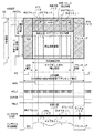
[装置構成]本発明に係る撮像装置は、特にデジタルビデオカメラやデジタルスチルカメラ(以下、カメラ)に有用である。このため、以下では、本発明に係る撮像装置をCMOSイメージセンサを搭載するデジタルカメラに適用した例について、図1及び図2を参照して説明する。 [Apparatus Configuration] The imaging apparatus according to the present invention is particularly useful for a digital video camera and a digital still camera (hereinafter referred to as a camera). Therefore, in the following, an example in which the imaging device according to the present invention is applied to a digital camera equipped with a CMOS image sensor will be described with reference to FIGS.
図1において、レンズ101は、被写体の光像を撮像素子103の撮像面に収束させる。絞り102は、被写体像の光量を調節するAE(自動露出制御)を行い、撮像される画像を適切な輝度レベルに保つように駆動される。
In FIG. 1, the
撮像素子103は、被写体の光像を電気信号に変換するCMOSイメージセンサ(以下、CMOSセンサ)である。
The
図2に示すように、CMOSセンサ103は、複数の画素が行方向(水平方向)及び列方向(垂直方向)において2次元に配列された有効画素部として光電変換素子であるフォトダイオードに光が照射される有効画素領域203を有する。また、CMOSセンサ103は、有効画素領域203の行方向または列方向の端部に設けられた遮光画素部として、アルミ薄膜等の遮光膜により光の照射が数列から数10列にわたって遮光される水平オプティカルブラック(以下、HOB)領域201と、アルミ薄膜等の遮光膜により光の照射が数ラインから数十ラインにわたって遮光される垂直オプティカルブラック(以下、VOB)領域202とに区分される。
As shown in FIG. 2, the
同期信号発生器(以下、SSG)104は、水平同期信号(以下、HD信号)及び垂直同期信号(以下、VD信号)を生成する。 A synchronization signal generator (hereinafter referred to as SSG) 104 generates a horizontal synchronization signal (hereinafter referred to as HD signal) and a vertical synchronization signal (hereinafter referred to as VD signal).
タイミングジェネレータ(以下、TG)105は、CMOSセンサ103を駆動させる各種制御信号をHD信号及びVD信号に同期して発生する。
A timing generator (hereinafter referred to as TG) 105 generates various control signals for driving the
A/D変換器106はCMOSセンサ103から出力されるアナログ信号をデジタル画像信号に変換する。
The A /
OBクランプ回路107は、A/D変換器106のOB期間の出力値を所定の値に固定する。
The
列オフセット検出回路108は、OBクランプ回路107から出力された画像信号に含まれる列オフセット成分をVOB領域から抽出する。列オフセット除去回路111は、列オフセット検出回路108にて検出された列オフセットを有効画素領域203の撮像信号から減算する。
The column offset
ウィンドウ回路109は、列オフセット検出回路108及び列オフセット除去回路111を駆動するための制御信号を生成する。
The
システムコントローラ110は、各部を統括して制御して動作モードやパラメータを決定する。
The
信号処理回路112は、デジタル画像信号に対して補間処理や色変換処理、縮小や拡大などの変倍処理を行い、表示デバイスに表示可能な画像信号に変換すると共に、記憶媒体に合せてJPEG形式の画像データなどに変換する。
The
[センサ構成]図3を参照して、CMOSセンサ103の回路構成について説明する。図3において、垂直走査回路300は画素配列から特定の読み出し行を選択する。リセットトランジスタ(以下、リセットTr)301a〜301cはフォトダイオードに蓄積された光信号電荷をリセットする。転送トランジスタ(以下、転送Tr)302a〜302cはフォトダイオードに蓄積された光信号電荷を後述するフローティングディフュージョンに転送する。
[Sensor Configuration] The circuit configuration of the
フォトダイオード(以下、PD)303a〜303cは光電変換素子からなる。フローティングディフュージョン(以下、FD)304a〜304cは光信号電荷をFD電位に転換する。選択トランジスタ(以下、選択Tr)305a〜305cは特定行を選択して画素ソースフォロアを作動させてFD電位を垂直出力線204a〜204cに読み出す。
Photodiodes (hereinafter referred to as PD) 303a to 303c are composed of photoelectric conversion elements. Floating diffusions (hereinafter referred to as FD) 304a to 304c convert optical signal charges into FD potentials. The selection transistors (hereinafter referred to as selection Trs) 305a to 305c select a specific row, operate the pixel source follower, and read the FD potential to the
画素ソースフォロア(以下、画素SF)306a〜306cはFD電位を垂直出力線に読み出すバッファアンプである。 Pixel source followers (hereinafter referred to as pixels SF) 306a to 306c are buffer amplifiers that read the FD potential to the vertical output line.
基準電圧Vref307は列アンプ205a〜205cでの信号増幅用の基準として用いられる。308は読み出し回路の1画素信号の構成単位である。サンプルホールド回路(以下、S/H(N))309a〜309cはN信号を記憶する。サンプルホールド回路(以下、S/H(S))310a〜310cはS信号を記憶する。
The reference voltage Vref307 is used as a reference for signal amplification in the
また、m行目の行選択線(以下、PSEL_m)311、m行目のリセット信号線(以下、PRES_m)312、m行目の信号転送線(以下、PTX_m)313は、CMOSセンサ103を制御する信号線である。また、信号線(以下、PTN)314は、S/H(N)309への読み出し期間を決定し、信号線(以下、PTS)315、S/H(S)310への読み出し期間を決定する信号線である。
The m-th row selection line (hereinafter referred to as PSEL_m) 311, the m-th row reset signal line (hereinafter referred to as PRES_m) 312, and the m-th row signal transfer line (hereinafter referred to as PTX_m) 313 control the
320は水平出力線であり、選択トランジスタ(以下、選択Tr)316a〜316cは、各列のS/H(N)309の出力を水平出力線320に選択して読み出す。同様に、321は水平出力線であり、選択トランジスタ(以下、選択Tr)317a〜317cは、各列のS/H(S)310の出力を水平出力線321に選択して読み出す。
水平走査回路319は各列のS/H(N)309の出力およびS/H(S)310の出力から特定の読み出し列を選択する。318a〜318cは水平走査回路319から出力されるn〜n+2列目の選択信号Hn〜Hn+2である。
The
差動回路323は水平出力線320、321からの信号を受けてCMOSセンサ103の出力VOUTとして差動出力を行う。
The
なお、1画素信号の構成単位308に4つのトランジスタを持つ構成を例示したが、2種類以上のリセット電圧を用い、画素SFを不活性化・活性化させる方式を用いることで、選択Tr305を省略することもできる。また、FDおよびSFを複数のPDで共有する構造であってもよい。
Although a configuration in which four transistors are included in one pixel
次に図3及び図4を参照して、読み出し時における図3の信号線の動作タイミングについて説明する。 Next, the operation timing of the signal line in FIG. 3 at the time of reading will be described with reference to FIGS.
撮影動作が開始されてPD303a〜303cに光が入射されると、光信号電荷が発生し蓄積を開始する。垂直走査回路300により各行の走査が順次行われていき、m行目の走査に至るとPRES_m312がハイレベルになり、FD304a〜304cの信号がリセットされる。
When the photographing operation is started and light is incident on the PDs 303a to 303c, optical signal charges are generated and accumulation is started. Each row is sequentially scanned by the
次にPSEL_m311がハイレベルになり、リセットノイズを含むリセットレベルが画素SF306a〜306cを通じて垂直出力線204a〜204cへ読み出される。そして、垂直出力線204a〜204cに読み出されたリセットレベルと基準電圧Vref307との差分が列アンプ205a〜205cにて増幅されて出力される。
Next,
そして、この出力されたN信号を、PTN_m313がハイレベルの期間(以下、N読み期間)でS/H(N)309に記憶される。その後、PTX_m313をハイレベルにして、PD303a〜303cにて発生した電荷を、FD304a〜304cに読み出す。N信号と同様にして、画素SF306a〜306c、垂直出力線204a〜204c、列アンプ205a〜205cを通過した後に出力されるS信号は、PTS_mがハイレベルの期間(以下、S読み期間)にS/H(S)310に記憶される。
The output N signal is stored in S / H (N) 309 during a period when
このようにして読み出されS/H(N)309に記憶された各列のm行目のN信号は、水平走査回路319の出力信号318a〜318cにより制御される選択Tr316a〜316cを介して、水平出力線320に列ごとに順次読み出される。
The N signals in the m-th row of each column read out in this way and stored in the S / H (N) 309 are passed through the
同様に、読み出されS/H(S)310に記憶された各列のm行目のN信号は、水平走査回路319の出力信号318a〜318cにより制御される選択Tr317a〜317cを介して、水平出力線321に列ごとに順次読み出される。
Similarly, the N signals in the m-th row of each column read and stored in the S / H (S) 310 are selected Tr31 7 a to 31 7 c controlled by the output signals 318 a to 318 c of the
列ごとに並列に読み出されたm行目のN信号とS信号とは、差動信号としてそれぞれ差動回路323に入力されて、その差動出力がCMOSセンサ103のセンサ出力VOUTとなる。
The m-th row N signal and S signal read in parallel for each column are respectively input as differential signals to the
S信号は、N信号にPD303a〜303cで発生した光信号電荷による信号が加わったものである。これによりS信号とN信号との差動動作をなすことでCDS動作が行われる。そして、CMOSセンサ103のセンサ出力VOUTから、素子に起因するリセットノイズや1/fノイズが除去されて、撮像信号には列オフセットに加えて画素欠陥ノイズとRTS(ランダム・テレグラム・シグナル)ノイズとが重畳する様態で出力される。
The S signal is obtained by adding a signal due to optical signal charges generated in the PDs 303a to 303c to the N signal. Thus, the CDS operation is performed by performing a differential operation between the S signal and the N signal. Then, reset noise and 1 / f noise caused by the elements are removed from the sensor output VOUT of the
[実施形態1]次に図5を参照して、実施形態1の撮像装置の動作について説明する。
[Embodiment 1] Next, the operation of the image pickup apparatus of
図5は、本実施形態のCMOSセンサ103のタイミング信号及びのタイミング信号に同期して出力された出力信号を例示する図である。
FIG. 5 is a diagram illustrating a timing signal of the
図5において、TG105は、SSG104において生成されるHD信号及びVD信号からCMOSセンサ103を駆動する各種制御信号を生成する。CMOSセンサ103は、TG105で生成される制御信号のタイミングで、レンズ101及び絞り102を通過した光信号を電気信号へと変換する。
In FIG. 5, the
CMOSセンサ103から読み出されたアナログ信号は、A/D変換器106にてデジタル信号に変換され、OBクランプ回路107を介してOB期間を所定のレベルに固定された後に、列オフセット検出回路108及び列オフセット除去回路111へ出力される。
The analog signal read from the
ウィンドウ回路109は、HD信号及びVD信号を参照して、列オフセット検出回路108にVOB領域における列オフセットの垂直の検出期間を指示する検出許可信号VWDETと水平の検出期間を指示する検出許可信号HWINと巡回演算の回数をカウントするためのパルス信号CCLKとを供給する。
The
ウィンドウ回路109は、列オフセット除去回路111に有効画素領域における垂直の列オフセット除去期間を指示する除去許可信号VWCOLと水平の列オフセット除去期間を指示する除去許可信号HWINを供給する。
The
列オフセット検出回路108は、ウィンドウ回路109から供給された検出許可信号に従って列オフセットデータを算出する。
The column offset
そして、列オフセット除去回路111は、ウィンドウ回路109から供給された除去許可信号VWCOLに従い、列オフセット検出回路108により列ごとに算出された列オフセット成分を有効画素領域の撮像信号から減算して除去する。
Then, the column offset
列オフセット除去回路111から出力された画像データは、信号処理回路112において信号処理されて、表示デバイスや記録デバイスに適合する画像データへと変換される。
The image data output from the column offset
TG105は、同期信号であるHD信号、VD信号の他に、CMOSセンサ103から1画素ごとに信号を読み出すクロック信号としてHCLK信号をCMOSセンサ103に供給している。
The
HCLK信号は、CMOSセンサ103の内部の構成要素であるHOB、VOB、有効画素の各領域の画素信号を読み出すためにセンサ出力を1画素サイクル単位で制御し、読み出し禁止期間にセンサ出力を停止する読み出し制御信号である。
The HCLK signal controls the sensor output in units of one pixel cycle in order to read out the pixel signals in the HOB, VOB, and effective pixel areas that are the internal components of the
TG105は、さらに、センサ出力の黒の基準となる画素信号をVOB、HOBの各領域から選択、抽出するための制御信号(CLPOB信号)をOBクランプ回路107に供給している。
Further, the
CLPOB信号により抽出されたHOB、VOBの画素信号は、OBクランプ回路107において有効画素領域の撮像信号から減算・出力されることで、黒レベル変動のない安定したセンサ出力を得ることができる。
The HOB and VOB pixel signals extracted by the CLPOB signal are subtracted and output from the image pickup signal in the effective pixel area by the
PBLK信号のタイミングは、1水平期間中のセンサ出力が読み出しを停止しているブランキング期間Tblkを示している。 The timing of the PBLK signal indicates a blanking period Tblk in which the sensor output during one horizontal period stops reading.
また、CMOSセンサ103は、背景技術で述べたように、XYアドレス型の読み出し構造に起因して、読み出し列ごとに異なる素子特性のばらつきによって列ごとに異なるオフセットが重畳する、所謂、列オフセットが発生しやすい。列オフセットは、VOB、HOB、有効画素領域の各領域の読み出し経路を共通に持つ同じ列上に等しく発生する性質がある。
In addition, as described in the background art, the
また、CMOSセンサ103の出力には列オフセットの他にも、画素欠陥ノイズやRTSノイズが重畳しており、さらにはセンサ後段のアナログ回路やAD変換時の量子化ノイズ等のランダムノイズが重畳される。
In addition to the column offset, pixel defect noise and RTS noise are superimposed on the output of the
図5のセンサ出力(VOB)とセンサ出力(有効画素領域)の波形は、これらに重畳する列オフセットとその他のノイズの態様を模式的に示したものである。 The waveforms of the sensor output (VOB) and sensor output (effective pixel region) in FIG. 5 schematically show the column offset and other noise modes superimposed on them.
本発明の趣旨は、動画のフレームレートを下げないために1フレームに係るVOB領域を増やすことなく、列オフセットと他のノイズが重畳したVOB領域のセンサ出力から不要なノイズ成分を排除して、列オフセットのみを高精度に検出することにある。 The gist of the present invention is to eliminate unnecessary noise components from the sensor output in the VOB area where the column offset and other noise are superimposed without increasing the VOB area related to one frame so as not to reduce the frame rate of the moving image. It is to detect only the column offset with high accuracy.
図6は、本発明を実現するための列オフセット検出回路108の回路構成を示している。
FIG. 6 shows a circuit configuration of the column offset
図6において、500は列オフセット検出回路108に入力される撮像信号Xnであり、乗算器501(係数K1)の入力に接続される。乗算器501(係数K1)の出力と乗算器503(係数K2)の出力は、それぞれ加算器502の入力に接続される。加算器502の出力はラインメモリ504に入力される。ラインメモリ504の出力は乗算器503に入力されると共に、列オフセット検出回路108の出力505となる。
In FIG. 6,
その他、列オフセットの垂直検出領域を指示する垂直検出ウィンドウ信号506(VWDET)と水平検出領域を指示する水平検出ウィンドウ信号507(HWIN)が、ウィンドウ回路109から列オフセット検出回路108の各部に供給される。また、ラインメモリ504に初期値のリロードを指示するモードリセット信号508(RESM)が、TG105から列オフセット検出回路108の各部に供給される。
In addition, a vertical detection window signal 506 (VWDET) indicating the vertical detection area of the column offset and a horizontal detection window signal 507 (HWIN) indicating the horizontal detection area are supplied from the
次に、列オフセット検出回路108の動作について説明する。
Next, the operation of the column offset
撮像信号Xnは、乗算器501、乗算器503、加算器502、ラインメモリ504とで構成される巡回積分回路に入力されて、垂直データ間の巡回演算が行われる。ラインメモリ504には、水平画素ごとに(列ごとに個別に)値を有する巡回演算値Ynが逐次、更新されて記憶される。
The imaging signal Xn is input to a cyclic integration circuit including a
巡回演算値Ynの演算式は下記式1で示される。サフィックスnは巡回演算の回数を表しており、1ラインごとに更新される。
The calculation formula of the cyclic calculation value Yn is shown by the following
巡回係数 : K1、K2(=1−K1)
巡回演算値 : Yn←K1・Xn+K2・Yn−1・・・(1)
図6の例では、巡回係数として、K1=1/64、K2=63/64が設定されており、1対63の比率で、撮像信号Xnに対して加重平均による演算が巡回的に繰り返される。
Cyclic coefficient: K1, K2 (= 1-K1)
Cyclic calculation value: Yn ← K1 · Xn + K2 · Yn−1 (1)
In the example of FIG. 6, K1 = 1/64 and K2 = 63/64 are set as the cyclic coefficients, and the calculation based on the weighted average is cyclically repeated for the imaging signal Xn at a ratio of 1:63. .
ラインメモリ504は、水平検出ウィンドウ信号HWINで示される1水平データ分の画素データを保持できる。
The
そして、動画撮影の最初のフレームを始動するVD信号に同期して、システムコントローラ110がTG105を介してモードリセット信号508(RESM)によりラインメモリ504に初期値のリロードを指示する。
Then, in synchronization with the VD signal that starts the first frame of moving image shooting, the
その後に、巡回積分回路では、垂直検出ウィンドウ信号VWDETと水平検出ウィンドウ信号HWINで示された列オフセット検出領域内で、これらの動作が水平画素ごとに順次行われる。 Thereafter, in the cyclic integration circuit, these operations are sequentially performed for each horizontal pixel in the column offset detection region indicated by the vertical detection window signal VWDET and the horizontal detection window signal HWIN.
垂直検出ウィンドウ信号VWDET期間に、複数回の巡回演算の後にラインメモリ518に記憶・保持された巡回演算値が、検出された列オフセットデータとして、列オフセット除去回路111に読み出されて列オフセットの除去が行われる。
In the period of the vertical detection window signal VWDET, the cyclic calculation value stored and held in the line memory 518 after a plurality of cyclic calculations is read to the column offset
図7は、動画撮影の際に連続して読み出された各フレーム画像から列オフセットを検出・補正する処理を示し、図8は、各フレーム画像から列オフセットが検出されて補正データが演算される様子を示している。 FIG. 7 shows a process for detecting / correcting a column offset from each frame image continuously read at the time of moving image shooting. FIG. 8 shows a column offset is detected from each frame image, and correction data is calculated. It shows how it works.
VOB領域は全部で64ラインある。このVOB領域は垂直方向に16ラインずつの4つの検出ブロックに分割される。 The VOB area has a total of 64 lines. This VOB area is divided into four detection blocks each having 16 lines in the vertical direction.
動画撮影のまず最初に、巡回演算式1の初期値0で第1フレームのVOB領域から列オフセットが検出されて、その結果が有効画素領域の撮像信号から減算されることで列オフセットが除去される。第1フレーム用のVOB領域は、VOB領域の最初の16ラインで指定されたブロック1の領域である。
At the beginning of moving image shooting, a column offset is detected from the VOB area of the first frame with the
次の第2フレームでは、第1フレームの列オフセットデータを巡回演算値として引き継いで第2フレーム用のVOB領域から列オフセットが検出されて、その結果が有効画素領域の撮像信号から減算されることで列オフセットが除去される。第2フレーム用のVOB領域は、第1フレームのVOB領域に続く次の16ラインで指定されたブロック2の領域である。
In the next second frame, the column offset data of the first frame is taken over as the cyclic calculation value, and the column offset is detected from the VOB area for the second frame, and the result is subtracted from the imaging signal of the effective pixel area. The column offset is removed. The VOB area for the second frame is an area of the
次の第3フレームでは、第2フレームの列オフセットデータを巡回演算値としてさらに引き継いで第3フレーム用のVOB領域から列オフセットが検出され、その結果が有効画素領域の撮像信号から減算されることで列オフセットが除去される。第3フレーム用のVOB領域は、第2フレームのVOB領域に続く次の16ラインで指定されたブロック3の領域である。 In the next third frame, the column offset data of the second frame is further taken over as the cyclic calculation value, and the column offset is detected from the VOB area for the third frame, and the result is subtracted from the imaging signal of the effective pixel area. The column offset is removed. The VOB area for the third frame is an area of the block 3 designated by the next 16 lines following the VOB area of the second frame.
次の第4フレームでは、第3フレームの列オフセットデータを巡回演算値としてさらに引き継いで第4フレーム用のVOB領域から列オフセットが検出され、その結果が有効画素領域の撮像信号から減算されることで列オフセットが除去される。第4フレーム用のVOB領域は、第3フレームのVOB領域に続く最後の16ラインで指定されたブロック4の領域である。そして、第4フレームにおいて全てのVOB領域が読み出される。 In the next fourth frame, the column offset data of the third frame is further taken over as the cyclic calculation value, and the column offset is detected from the VOB area for the fourth frame, and the result is subtracted from the imaging signal of the effective pixel area. The column offset is removed. The VOB area for the fourth frame is an area of the block 4 designated by the last 16 lines following the VOB area of the third frame. Then, all VOB areas are read in the fourth frame.
そして、次の第5フレームでは、第4フレームの列オフセットデータを巡回演算値としてさらに引き継いで第5フレーム用のVOB領域から列オフセットが検出され、その結果が有効画素領域の撮像信号から減算されることで列オフセットが除去される。第5フレーム用のVOB領域は、再びVOB領域の最初の16ラインで指定されたブロック1の領域に戻り、第1フレーム用のVOB領域と同じ領域となる。以降、4フレーム単位で全VOB領域の読み出しが繰り返される。
In the next fifth frame, the column offset data of the fourth frame is further taken over as the cyclic calculation value, and the column offset is detected from the VOB area for the fifth frame, and the result is subtracted from the imaging signal of the effective pixel area. This removes the column offset. The VOB area for the fifth frame again returns to the area of
ところで、列オフセットの検出領域であるVOBには既に説明したように画素欠陥ノイズやRTSノイズが重畳しており、列オフセットの検出精度を劣化させる誤差要因となりうる。 By the way, as described above, pixel defect noise and RTS noise are superimposed on the VOB which is the column offset detection area, which may cause an error factor to deteriorate the column offset detection accuracy.
さらに、列オフセットの検出領域においてRTSノイズの発生頻度が高い画素ソースフォロアが偏在しており、検出ブロックごとにRTSノイズの影響による誤差量は大きく異なる。 Further, pixel source followers with high RTS noise occurrence frequency are unevenly distributed in the column offset detection region, and the error amount due to the influence of the RTS noise is greatly different for each detection block.
図9は特定の画素列上に発生するRTSノイズによる誤差量に関して、各検出ブロックごとの誤差量と全検出ブロックでの誤差量との関係を模式的に示している。 FIG. 9 schematically shows the relationship between the error amount for each detection block and the error amount in all detection blocks with respect to the error amount due to RTS noise generated on a specific pixel column.
図9で検出ブロックごとの誤差量はフレームごとに同一の検出ブロックのみを繰り返して読み出した場合の検出ブロック内の16ラインの加重平均による誤差量を表している。 In FIG. 9, the error amount for each detection block represents the error amount by the weighted average of 16 lines in the detection block when only the same detection block is repeatedly read for each frame.
全検出ブロックでの誤差量は全検出ブロックを4フレーム単位で繰り返して読み出した場合の全検出領域64ラインの加重平均による誤差量を表している。 The error amount in all detection blocks represents the error amount due to the weighted average of all detection area 64 lines when all detection blocks are repeatedly read out in units of 4 frames.
図9の例では、RTSノイズが検出ブロック1の16ラインに偏って高頻度で発生しており、検出ブロック1の16ラインのみの加重平均による誤差量が画像に影響を及ぼす許容レベルを超える結果となる場合を示している。
In the example of FIG. 9, RTS noise is generated with high frequency biased toward 16 lines of the
RTSノイズの発生頻度を全VOB領域にわたって全画素で低レベルに抑えることは、撮像素子の製造プロセス上、非常に困難である。そして、RTSノイズの発生頻度は局所的に偏在しており、しかも個体差があるため許容レベルを超える検出ブロックが何れになるかは撮像素子ごとにまちまちである。 It is very difficult to suppress the frequency of occurrence of RTS noise to a low level in all pixels over the entire VOB region in terms of the manufacturing process of the image sensor. The frequency of occurrence of RTS noise is unevenly distributed locally, and there are individual differences, so which detection block exceeds the allowable level depends on the image sensor.
しかし、RTSノイズがどのように局所的に偏在したとしても、その発生頻度を全VOB領域の中で平均してみた場合に、一定の割合以下に抑えた撮像素子を製造することは十分に可能である。 However, no matter how locally the RTS noise is unevenly distributed, it is sufficiently possible to manufacture an image pickup device that suppresses the occurrence frequency to a certain ratio or less when the occurrence frequency is averaged over the entire VOB region. It is.
そして、図9は、このような撮像素子において、検出ブロック2、3、4でのRTSノイズの発生頻度が低いことで、検出ブロック1をこれらに含めた全検出ブロックの64ラインの加重平均による誤差量として、許容レベル以下に低減する様子を示している。
FIG. 9 shows a weighted average of 64 lines of all the detection blocks including the
図10は、VOB領域の各検出ブロックにおける同じ列上の画素信号のデータ分布を示しており、以下では、図10を参照してRTSノイズの発生頻度を検出する方法の一例について説明する。 FIG. 10 shows the data distribution of pixel signals on the same column in each detection block in the VOB area. Hereinafter, an example of a method for detecting the occurrence frequency of RTS noise will be described with reference to FIG.
この例では、列データのメディアン値に対して所定の閾値を設ける。そして、この閾値から外れたデータをRTSノイズとみなして発生個数を計数する。計数値の大きなものほどRTSノイズの発生頻度が高いと判断する。このようにして求めたRTSノイズの発生頻度の検出値と加重平均による誤差量との関係には強い相関性が得られる。 In this example, a predetermined threshold is provided for the median value of the column data. Then, the number of occurrences is counted by regarding data deviating from the threshold as RTS noise. It is determined that the higher the count value, the higher the occurrence frequency of RTS noise. A strong correlation is obtained in the relationship between the detected value of the occurrence frequency of the RTS noise thus obtained and the error amount by the weighted average.
RTSノイズの発生頻度を全VOB領域にわたって全画素で低レベルに抑えることは、撮像素子の製造プロセス上、非常に困難である。そして、RTSノイズの発生頻度は局所的に偏在しており、しかも個体差があるため許容レベルを超える検出ブロックが何れになるかは撮像素子ごとにまちまちである。 It is very difficult to suppress the frequency of occurrence of RTS noise to a low level in all pixels over the entire VOB region in terms of the manufacturing process of the image sensor. The frequency of occurrence of RTS noise is unevenly distributed locally, and there are individual differences, so which detection block exceeds the allowable level depends on the image sensor.
そこで、撮像素子ごとに、予め、RTSノイズの発生頻度を検出ブロックごとに検出しておいて、その検出結果を当該撮像素子が搭載された撮像装置に記憶しておく。この調整手順は、撮像素子の製造ラインの工程上で行っても良いし撮像装置に調整モード等を設けて行ってもよい。 Therefore, for each image sensor, the frequency of occurrence of RTS noise is detected in advance for each detection block, and the detection result is stored in the image pickup apparatus on which the image sensor is mounted. This adjustment procedure may be performed in the process of the production line of the imaging device, or may be performed by providing an adjustment mode or the like in the imaging device.
本実施形態のようにフレーム単位で検出領域を切り換える構成をなすことで、全検出領域を用いた加重平均によって誤差量を許容レベル以下に低減することが可能である。 By configuring the detection area to be switched in units of frames as in the present embodiment, it is possible to reduce the error amount to an allowable level or less by a weighted average using all the detection areas.
本実施形態では4フレームで全検出領域64ラインを読み出す構成としたが、撮像素子のRTSノイズの発生頻度に基づいて、十分なノイズ低減効果を得るために、適宜、検出領域の拡張を図るべきである。 In this embodiment, 64 lines of all detection areas are read out in 4 frames. However, in order to obtain a sufficient noise reduction effect based on the frequency of occurrence of RTS noise in the image sensor, the detection area should be appropriately expanded. It is.
本実施形態では、1フレームあたりの検出ライン数を増やすことなくRTSノイズの影響を低減することができるため、動画のフレームレートを落とすこともなく、消費電力の増加につながる読み出しの動作スピードを上げる必要もない。 In this embodiment, since the influence of RTS noise can be reduced without increasing the number of detection lines per frame, the read operation speed that leads to an increase in power consumption is increased without reducing the frame rate of the moving image. There is no need.
なお、本実施形態においては、説明の便宜上、列オフセットの検出領域にVOB画素を割り当てて、全て、動作の説明を行っている。 In the present embodiment, for convenience of explanation, VOB pixels are assigned to the column offset detection area, and all operations are explained.
しかしながら、本発明の趣旨によれば、画素ソースフォロアに電気的にフォトダイオードが接続されない状態で読み出しが行われる、所謂、ダミー画素を検出領域として割り当てても同様の効果を得ることができる。 However, according to the gist of the present invention, the same effect can be obtained even if a so-called dummy pixel, in which reading is performed without a photodiode being electrically connected to the pixel source follower, is assigned as a detection region.
むしろ、ダミー画素にはフォトダイオードに起因する画素欠陥ノイズが発生しない分、列オフセットの検出には有利である。また、この場合の有効画素の黒レベルの基準は、HOB画素のクランプ動作により得ることができる。 Rather, the dummy pixel is advantageous in detecting the column offset because pixel defect noise caused by the photodiode is not generated. In this case, the reference of the black level of the effective pixel can be obtained by the clamping operation of the HOB pixel.
また、本実施形態においては、式1の巡回係数として、K1=1/64、K2=63/64を用いた加重平均による巡回演算を例示している。
Further, in the present embodiment, a cyclic calculation by weighted average using K1 = 1/64 and K2 = 63/64 is illustrated as the cyclic coefficient of
しかし、本発明によれば、例えば式1に対して、K1=1/16、K2=1を用いた加重平均を16回繰り返して巡回演算させることにより、検出ブロックごとに加重平均値を算出して、この値を巡回演算値として次のフレームに引き継ぐことも可能である。
However, calculated according to the present invention, for example for
[実施形態2]実施形態1では、1フレームあたり16ラインの検出領域を割り当てる構成としたが、フレームごとに検出領域を切り換えれば、1フレームあたりの検出ライン数をさらに減らして動画のフレームレートを向上させることも可能である。このことを実現したのが、以下に説明する実施形態2である。
[Embodiment 2] In
図11は、巡回演算値の収束の様子を示している。 FIG. 11 shows how the cyclic calculation values converge.
巡回演算式1の場合、例えば巡回係数Kが(1/64)であれば、1回の巡回演算で入力データXnの(1/64)が巡回演算値として加重平均がなされるため、これを128回繰り返すことで、ほぼ演算値を収束させることができる。
In the case of the
実施形態2では1フレームのVOBの検出ライン数が16ラインの設定であり、1フレームあたり16回の巡回演算ができるので、最初の8フレームでほぼ演算を収束させて正しい列オフセットを検出することが可能である。 In the second embodiment, the number of detection lines for one frame of VOB is set to 16 lines, and 16 cyclic operations can be performed per frame, so that the operation is almost converged in the first 8 frames to detect a correct column offset. Is possible.
動画のフレームレートが30[フレーム/秒]の場合に、8フレームに要する時間は、0.27(=8/30)秒である。動画の描画開始から列オフセットが正しく検出・補正されて動画像から縦縞が消えるまでに、0.27秒の時間がかかることを意味しており、これ以上に巡回演算の収束時間を延ばすことは動画品質上好ましくない。 When the frame rate of the moving image is 30 [frames / second], the time required for 8 frames is 0.27 (= 8/30) seconds. This means that it takes 0.27 seconds from the start of video rendering until the column offset is correctly detected and corrected and the vertical stripes disappear from the moving image. Not good for video quality.
列オフセットの最大値は撮像素子の出力で数mV〜数10mV見込まれており、このような列オフセットを検出して補正するために許容できる収束時間を満足する巡回係数K1の上限値が、K1=1/64(K2=63/64)である。 The maximum value of the column offset is expected to be several mV to several tens of mV at the output of the image sensor, and the upper limit value of the cyclic coefficient K1 that satisfies an acceptable convergence time for detecting and correcting such a column offset is K1. = 1/64 (K2 = 63/64).
また、1箇所のRTSノイズの発生に対して巡回係数K1(1/64)を乗じた値が巡回演算値の誤差となる。 Also, a value obtained by multiplying the occurrence of one RTS noise by the cyclic coefficient K1 (1/64) is an error in the cyclic calculation value.
巡回係数K1を(1/32)などに上げれば巡回演算の収束時間が短縮するが、RTSノイズによる誤差を増大させる結果となるため、巡回係数K1は容易に上げることができない。 Increasing the cyclic coefficient K1 to (1/32) or the like shortens the convergence time of the cyclic calculation, but increases the error due to RTS noise, so the cyclic coefficient K1 cannot be easily increased.
1フレームあたりの検出ライン数を減らせばその分だけ、動画のフレームレートを今より向上させることができる。しかし、例えば1フレームあたりの検出ライン数を16ラインから半分の8ラインに変更すると、巡回演算の収束時間は2倍の16フレームにあたる0.54(=16/30)秒に増大してしまう。 If the number of detection lines per frame is reduced, the frame rate of the moving image can be improved by that much. However, for example, if the number of detection lines per frame is changed from 16 lines to half of 8 lines, the convergence time of the cyclic operation increases to 0.54 (= 16/30) seconds, which is 16 frames twice.
1フレームあたりの検出ライン数を減らすためには、巡回演算の収束時間が増大してしまうという上記の問題を回避する工夫が併せて必要となる。 In order to reduce the number of detection lines per frame, it is necessary to devise a technique for avoiding the above-described problem that the convergence time of the cyclic calculation increases.
そのために実施形態2では、動画の最初のフレーム画像の読み出しに先立ち、短期間のうちに巡回演算を収束させて列オフセットの検出を行う。そして、これを列オフセット検出値の初期値として、動画の最初のフレームから精度よく列オフセットの補正を行う動作を実施形態1に追加している。 Therefore, in the second embodiment, prior to reading out the first frame image of a moving image, the column calculation is detected by converging the cyclic calculation within a short period. Then, with this as the initial value of the column offset detection value, an operation for accurately correcting the column offset from the first frame of the moving image is added to the first embodiment.
図12は、動画撮影の際に連続して読み出された各フレーム画像から列オフセットを検出・補正する処理を示し、図13は、各フレーム画像から列オフセットが検出されて補正データが演算される様子を示している。 FIG. 12 shows a process for detecting / correcting a column offset from each frame image continuously read during moving image shooting, and FIG. 13 shows a column offset is detected from each frame image and correction data is calculated. It shows how it works.
VOB領域は全部で64ラインある。このVOB領域は垂直方向に8ラインずつの8つの検出ブロックに分割される。 The VOB area has a total of 64 lines. This VOB area is divided into eight detection blocks each having eight lines in the vertical direction.
動画の読み出しに先立ち、最初にダミーフレームが設けられており、巡回演算の初期値0でダミーフレームのVOB領域から列オフセットが検出される。ダミーフレーム用のVOB領域は、64ラインで指定された全VOB領域である。ダミーフレームにおいては、短期間に動画の第1フレームに動作を移行するために、VOB領域のみで有効画素領域の画素信号の読み出しは行われない。 Prior to reading out a moving image, a dummy frame is first provided, and a column offset is detected from the VOB area of the dummy frame with an initial value of 0 in the cyclic operation. The dummy frame VOB area is an entire VOB area designated by 64 lines. In the dummy frame, in order to shift the operation to the first frame of the moving image in a short time, the pixel signal of the effective pixel region is not read out only in the VOB region.
さらに、ダミーフレームにおいては、巡回係数K(1/64)に対して巡回演算を収束させて正しい列オフセットを検出するために、64ラインで指定された全VOB領域が総じて2回繰り返して読み出される。 Further, in the dummy frame, all VOB areas designated by 64 lines are read out twice in total in order to converge a cyclic operation on the cyclic coefficient K (1/64) and detect a correct column offset. .
ダミーフレームにおけるVOB128ラインの読み出し時間は、通常の動画の1フレームの読み出し時間(1/30)秒に対して時間的に十分短いので、動画の描画開始までのロスタイムとしては何ら問題とならない。
Since the reading time of the
ダミーフレームの列オフセットデータを巡回演算値の初期値として引き継いで、第1フレームのVOB領域から列オフセットが検出され、その結果が有効画素領域の撮像信号から減算されることで列オフセットが除去される。第1フレーム用のVOB領域は、VOB領域の最初の8ラインで指定されたブロック1の領域である。
The column offset data of the dummy frame is inherited as the initial value of the cyclic calculation value, the column offset is detected from the VOB area of the first frame, and the result is subtracted from the imaging signal of the effective pixel area, thereby removing the column offset. The The VOB area for the first frame is an area of the
次の第2フレームでは、第1フレームの列オフセットデータを巡回演算値として引き継いで第2フレーム用のVOB領域から列オフセットが検出され、その結果が有効画素領域の撮像信号から減算されることで列オフセットが除去される。第2フレーム用のVOB領域は、第1フレームのVOB領域に続く次の8ラインで指定されたブロック2の領域である。
In the next second frame, the column offset data of the first frame is taken over as a cyclic calculation value, the column offset is detected from the VOB area for the second frame, and the result is subtracted from the imaging signal of the effective pixel area. Column offset is removed. The VOB area for the second frame is an area of the
以降のフレームでは、同様にして、前のフレームの列オフセットデータを巡回演算値としてさらに引き継いで、当該フレーム用のVOB領域から列オフセットが検出され、その結果が有効画素領域の撮像信号から減算されることで列オフセットが除去される。当該フレーム用のVOB領域は、前のフレームのVOB領域に続く次の8ラインで指定されたブロック領域である。このようにして、順次、第3フレームから第7フレームまでの読み出しの動作が行われる。 Similarly, in subsequent frames, the column offset data of the previous frame is further taken over as the cyclic operation value, and the column offset is detected from the VOB region for the frame, and the result is subtracted from the imaging signal of the effective pixel region. This removes the column offset. The VOB area for the frame is a block area designated by the next eight lines following the VOB area of the previous frame. In this manner, the reading operation from the third frame to the seventh frame is sequentially performed.
第8フレームでは、第7フレームの列オフセットデータを巡回演算値としてさらに引き継いで第7フレーム用のVOB領域から列オフセットが検出され、その結果が有効画素領域の撮像信号から減算されることで列オフセットが除去される。第8フレーム用のVOB領域は、第7フレームのVOB領域に続く最後の8ラインで指定されたブロック8の領域である。そして、第8フレームにおいて全てのVOB領域が読み出される。 In the eighth frame, the column offset data of the seventh frame is further taken over as a cyclic calculation value, and the column offset is detected from the VOB region for the seventh frame, and the result is subtracted from the imaging signal of the effective pixel region. The offset is removed. The VOB area for the eighth frame is an area of the block 8 designated by the last 8 lines following the VOB area of the seventh frame. Then, all VOB areas are read in the eighth frame.
そして、次の第9フレームでは、第8フレームの列オフセットデータを巡回演算値としてさらに引き継いで第9フレーム用のVOB領域から列オフセットが検出され、その結果が有効画素領域の撮像信号から減算されることで列オフセットが除去される。第9フレーム用のVOB領域は、再びVOB領域の最初の8ラインで指定されたブロック1の領域に戻り、第1フレーム用のVOB領域と同じ領域となる。以降、8フレーム単位で全VOB領域の読み出しの過程が繰り返される。
In the next ninth frame, the column offset data of the eighth frame is further taken over as the cyclic calculation value, and the column offset is detected from the VOB region for the ninth frame, and the result is subtracted from the imaging signal of the effective pixel region. This removes the column offset. The VOB area for the ninth frame returns to the area of the
このようにして、実施形態2では、動画の最初のフレーム画像の読み出しに先立ち、ダミーフレームを挿入して巡回演算の収束時間の問題の解決を図っている。 Thus, in the second embodiment, prior to reading out the first frame image of a moving image, a dummy frame is inserted to solve the problem of the convergence time of the cyclic calculation.
その上で、1フレームあたりの検出ライン数を8ラインに変更することで、実施形態1に対してさらに動画のフレームレートを向上させることが可能である。 In addition, by changing the number of detection lines per frame to 8 lines, it is possible to further improve the frame rate of the moving image with respect to the first embodiment.
[実施形態3」次に、図14及び図15を参照して、実施形態3について説明する。 [Third Embodiment] Next, a third embodiment will be described with reference to FIGS.
図14は、動画撮影の際に連続して読み出された各フレームから列オフセットを検出・補正する処理を示し、図15は、各フレームから列オフセットが検出されて補正データを演算する様子を示している。 FIG. 14 shows a process for detecting and correcting a column offset from each frame continuously read out during moving image shooting. FIG. 15 shows how a column offset is detected from each frame and correction data is calculated. Show.
ここでは、動画撮影の前に、予め撮像素子のRTSノイズの発生頻度について検出が済んでおり、図9に示すように、検出ブロック1の誤差量が突出しており、ブロック3の誤差量が最も小さい場合を例として説明する。
Here, detection of RTS noise occurrence frequency of the image sensor is completed in advance before moving image shooting. As shown in FIG. 9, the error amount of the
動画動作のまず最初に、撮像装置に記憶されている撮像素子のRTSノイズの発生頻度に関するブロックごとの検出結果に基づいて、最も加重平均による誤差量が小さいと考えられる検出ブロック3がVOBの検出領域として指定される。 First of all, the detection block 3 that is considered to have the smallest error amount due to the weighted average is detected by the detection block 3 based on the detection result for each block related to the occurrence frequency of the RTS noise of the image sensor stored in the imaging device. Specified as an area.
検出ブロック3を指定して列オフセットの検出を行うのに最も単純な方法は、撮像素子がCMOSセンサで構成される場合には、センサ内部の垂直走査回路の制御により他のブロック領域を読み飛ばして検出ブロック3のみを読み出すことである。 The simplest method for detecting the column offset by designating the detection block 3 is to skip other block areas under the control of the vertical scanning circuit inside the sensor when the image sensor is constituted by a CMOS sensor. Thus, only the detection block 3 is read out.
しかしながら、撮像素子が読み飛ばしのできないCCDセンサであっても、列オフセット検出回路108において、他のブロック領域を読み出す際に式1の巡回係数をK1=0、K2=1に切り換えて加重平均の割合を変更することで対応可能である。この場合、検出ブロック3以外の領域の加重割合はゼロとなり、加重平均による演算結果は読み飛ばした場合の結果と等しい。
However, even if the image sensor is a CCD sensor that cannot be skipped, the column offset
そして、巡回演算の初期値0で第1フレームのVOB領域として指定された検出ブロック3から列オフセットが検出され、その結果が有効画素領域の撮像信号から減算されることで列オフセットが除去される。
Then, the column offset is detected from the detection block 3 designated as the VOB region of the first frame with the
次の第2フレームでは、第1フレームの列オフセットデータを巡回演算値として引き継いで、同じくVOB領域として指定された検出ブロック3から列オフセットが検出され、その結果が有効画素領域の撮像信号から減算されることで列オフセットが除去される。 In the next second frame, the column offset data of the first frame is taken over as the cyclic operation value, and the column offset is detected from the detection block 3 which is also designated as the VOB region, and the result is subtracted from the imaging signal of the effective pixel region. As a result, the column offset is removed.
次の第3フレームも同様に、前のフレームの列オフセットデータを巡回演算値として引き継いで、VOB領域として指定された検出ブロック3から列オフセットが検出され、その結果が有効画素領域の撮像信号から減算されることで列オフセットが除去される。 Similarly, in the next third frame, the column offset data of the previous frame is taken over as the cyclic calculation value, and the column offset is detected from the detection block 3 designated as the VOB region, and the result is obtained from the imaging signal in the effective pixel region. The column offset is removed by subtraction.
以降、各フレームでVOB領域として検出ブロック3が指定されて読み出しが繰り返される。 Thereafter, the detection block 3 is designated as the VOB area in each frame, and reading is repeated.
このようにして、検出領域を分割して、分割された検出ブロックごとにRTSノイズの発生頻度の検出結果に基づいて検出ブロックを取捨選択する。そして、ノイズ発生頻度の高い領域を避けて低い領域での加重平均による巡回演算により、RTSノイズの影響を抑え、RTSノイズによる誤差量を許容レベル以下に低減することが可能である。 In this manner, the detection area is divided, and the detection blocks are selected based on the detection result of the RTS noise occurrence frequency for each of the divided detection blocks. Then, the influence of RTS noise can be suppressed and the amount of error due to RTS noise can be reduced to an allowable level or less by cyclic calculation based on weighted averaging in a low area while avoiding areas where noise is frequently generated.
本実施形態でも、十分なノイズ低減効果を得るために、撮像素子のRTSノイズの発生頻度に基づいて、適宜、検出領域や分割ブロック数の拡張を図るべきである。 Also in this embodiment, in order to obtain a sufficient noise reduction effect, the detection area and the number of divided blocks should be appropriately expanded based on the frequency of occurrence of RTS noise of the image sensor.
また、本実施形態においても、画素ソースフォロアに電気的にフォトダイオードが接続されない状態で読み出しが行われる、所謂、ダミー画素を検出領域として割り当てても同様の効果を得ることができる。 Also in this embodiment, the same effect can be obtained by assigning a so-called dummy pixel as a detection region in which reading is performed in a state where a photodiode is not electrically connected to the pixel source follower.
また、上述した加重平均の動作は以下に説明する実施形態4および実施形態5においても利用される。 Further, the above-mentioned weighted average operation is also utilized in embodiments 4 and Embodiment 5 described below.
[実施形態4]VOBの検出領域においてRTSノイズの発生頻度が高い領域が偏在することは既に説明した。ところが、画素ソースフォロアの素子の温度特性や経時変化によって、これらの偏在箇所がしばしば移動する場合がある。 [Embodiment 4] As described above, the region where the frequency of occurrence of RTS noise is high is unevenly distributed in the VOB detection region. However, these unevenly distributed locations often move depending on the temperature characteristics of the pixel source follower elements and changes with time.
そこで、実施形態4として、撮像中にRTSノイズによる誤差量を検出ブロック単位で算出して所定以内にある検出ブロックを採択する手順を組み込むことで、温度などの周囲環境や経時変化にもリアルタイムに対応できるように工夫した方法について説明する。 Therefore, as a fourth embodiment, by incorporating a procedure for calculating an error amount due to RTS noise for each detection block during imaging and adopting a detection block within a predetermined range, the ambient environment such as temperature and changes over time can be realized in real time. The method devised so that it can respond is explained.
以下では、実施形態3と構成や動作の異なる部分を中心に説明する。 Below, it demonstrates centering on the part from which Embodiment 3 differs in a structure and operation | movement.
撮像装置の基本的な構成は実施形態3と同様であるが、RTSノイズによる誤差量を算出する手段が撮像装置に追加される点が異なる。 The basic configuration of the imaging apparatus is the same as that of the third embodiment, except that means for calculating an error amount due to RTS noise is added to the imaging apparatus.
図16は、RTSノイズによる誤差量を算出する回路構成を、列オフセット検出回路108の内部に追加したものであり、図6に対して新たに追加された部分が破線枠内に示される誤差判定回路510である。
FIG. 16 is a diagram in which a circuit configuration for calculating an error amount due to RTS noise is added to the inside of the column offset
誤差判定回路510には、出力505を受けて検出された各列の列オフセット補正データの中から最大値を検出する最大値検出回路511と、同様に各列の列オフセット補正データの中から最小値を検出する最小値検出回路512とを含む。
The
さらに、最大値検出回路511の出力から最小値検出回路512の出力を減ずる減算器513と、減算器513の出力値を受けて、所定値以内にあるか否かを判定して判定結果を出力するレベル判定回路514とを含む。さらに、レベル判定回路514には、システムコントローラ110によりレジスタ値E0が設定可能なレジスタが接続される
そしてレベル判定回路514の出力516は、誤差判定の出力結果としてシステムコントローラ110に供給される。
Further, the
図17は、動画撮影の際に連続して読み出された各フレーム画像から列オフセットを検出・補正する処理を示し、図18は、各フレームから列オフセットが検出されて補正データを演算する様子を示している。 FIG. 17 shows a process for detecting / correcting a column offset from each frame image continuously read during moving image shooting, and FIG. 18 shows how the column offset is detected from each frame to calculate correction data. Is shown.
上述した実施形態3と同様に、VOB領域は全部で64ラインが設定されており、垂直方向に16ラインずつの4つの検出ブロックに分割される。 Similar to the third embodiment described above, the VOB area has 64 lines in total, and is divided into four detection blocks each having 16 lines in the vertical direction.
そして、撮像素子のRTSノイズの発生頻度については、図9と同じ特性を有する撮像素子を用いた場合を一例として動作を説明する。 As for the frequency of occurrence of RTS noise in the image sensor, the operation will be described by taking as an example a case where an image sensor having the same characteristics as in FIG. 9 is used.
すなわち、検出ブロック1の誤差量が突出すると共に許容量を超えており、検出ブロック2〜4が許容量以内にあり、検出ブロック3の誤差量が最も小さい場合について説明する。
That is, the case where the error amount of the
動画撮影のまず最初に、第1フレームの検出領域としてVOB領域の最初のラインから始まる16ラインの検出ブロック1が指定される。
First of all, the
式1の巡回係数が、K1=1/16、K2=1に設定される。そして、これらの巡回係数による加重平均を16回繰り返して巡回演算させることにより、検出ブロック1内の各列ごとに16ラインの加算平均値が算出される。
The cyclic coefficient of
算出された各列ごとの加重平均値は、垂直補正ウィンドウ信号VWCOL期間に読み出され、その結果が有効画素領域の撮像信号から減算されることで列オフセットが除去される。 The weighted average value for each column is calculated, read to the vertical correction window signal VWCOL period, column offset is removed by the result is subtracted from the image signal of the effective pixel region.
他方で、垂直補正ウィンドウ信号VWCOL期間に読み出された各列ごとの加重平均値は、図16に示した誤差判定回路510にも供給されて、最大値検出回路511と最小値検出回路512とにより最大値および最小値が検出・保持される。その差分値が列オフセット最大値となり、レベル判定回路514にてレジスタ値E0と比較される。そして、レジスタ値E0よりも大きな場合に、レベル判定回路514の出力線516からエラーが出力される。
On the other hand, the weighted average value for each column is read to the vertical correction window signal VWCOL period, it is also supplied to the
図19は各列ごとの加重平均値と算出された列オフセット最大値を示している。 Figure 19 shows a column offset maximum value calculated as the weighted average value of each column.
レジスタ値E0は、撮像素子により規定される列オフセットの上限値を超えたところの所定値が設定されており、通常、撮像素子の出力で見て数mV〜数10mVに相当する値である。そして、列オフセットの上限値を逸脱する列オフセット最大値に対して、判定結果としてエラーが出力される。 The register value E0 is set to a predetermined value that exceeds the upper limit value of the column offset defined by the image sensor, and is usually a value corresponding to several mV to several tens of mV when viewed from the output of the image sensor. An error is output as a determination result for the maximum column offset value that deviates from the upper limit value of the column offset.
この場合には、検出ブロック1にRTSノイズが偏在しており、そのために、RTSノイズによる誤差量が大きくなり、判定結果としてエラーが出力される。
In this case, RTS noise is unevenly distributed in the
エラーの判定結果はシステムコントローラ110に伝達されて記憶される。
The error determination result is transmitted to the
次の第2フレームでは、エラー判定結果を受けて、システムコントローラ110によりVOB領域として第1フレームのVOB領域に続く次の16ラインのブロック2が指定されて、検出ブロックが更新される。
In the next second frame, in response to the error determination result, the
その後は、第1フレームの場合と全く同様にして、列オフセット検出回路108では式1の巡回係数が、再び、K1=1/16、K2=1、巡回演算の初期値0に設定される。
Thereafter, in exactly the same manner as in the case of the first frame, the column offset
そして、これらの巡回係数による加重平均を16回繰り返して巡回演算させることにより、検出ブロック2内の各列ごとに16ラインの加重平均値が算出される。
Then, by weighted average is cyclically calculated repetitively 16 times using these cyclic coefficients, the weighted average of 16 lines for each column within
算出された各列ごとの加重平均値は、垂直補正ウィンドウ信号VWCOL期間に読み出され、その結果が有効画素領域の撮像信号から減算されることで列オフセットが除去される。 The weighted average value for each column is calculated, read to the vertical correction window signal VWCOL period, column offset is removed by the result is subtracted from the image signal of the effective pixel region.
他方で、垂直補正ウィンドウ信号VWCOL期間に読み出された各列ごとの加重平均値は、誤差判定回路510によって列オフセット最大値が算出されて、レベル判定回路514にてレジスタ値E0と比較される。
On the other hand, the weighted average value for each column is read to the vertical correction window signal VWCOL period is calculated column offset maximum value by the
今度は、第1フレームの場合と異なり検出ブロック2にはRTSノイズが偏在しておらず、そのために、RTSノイズによる誤差量は許容値内にあり、判定結果としては非エラーが出力される。
This time, unlike the case of the first frame, RTS noise is not unevenly distributed in the
非エラーの判定結果はシステムコントローラ110に伝達されて記憶される。
The determination result of non-error is transmitted to the
次の第3フレームでは、非エラー判定結果を受けて、システムコントローラ110によりVOB領域として第2フレームと同じ検出ブロック2が指定されて、検出ブロックが更新されない。
In the next third frame, the non-error determination result is received, and the
また、非エラー判定結果を受けて、第3フレーム以降のフレームでは、列オフセット検出回路108によるエラー判定は行われず、システムコントローラ110に伝達されて記憶された非エラーの判定結果は更新されない。
Further, in response to the non-error determination result, the error determination by the column offset
その後は、巡回演算式1において、初期値として直前のフレームである第2フレームの列オフセットデータ、すなわち検出ブロック2内の各列ごとに算出された16ラインの加重平均値が引き継がれる。
Thereafter, the
さらに、式1の巡回係数は、K1=1/64、K2=63/64に設定される。そして、これらの巡回係数による加重平均を16回繰り返して巡回演算させることにより、検出ブロック2内の各列ごとに16ラインの加重平均値が算出される。
Further, the cyclic coefficient of
算出された各列ごとの加重平均値は、垂直補正ウィンドウ信号(VWCOL)期間に読み出され、その結果が有効画素領域の撮像信号から減算されることで列オフセットが除去される。 The calculated weighted average value for each column is read during the vertical correction window signal (VWCOL) period, and the result is subtracted from the imaging signal of the effective pixel region, thereby removing the column offset.
次の第4フレームでは、先の非エラー判定結果を受けて、システムコントローラ110によりVOB領域として第2フレームと同じ検出ブロック2が指定されて、検出ブロックが更新されない。
In the next fourth frame, in response to the previous non-error determination result, the
その後は、巡回演算式1において、直前のフレームである第3フレームの列オフセットデータすなわち検出ブロック2内の各列ごとに算出された16ラインの加重平均値が引き継がれる。
Thereafter, in
巡回係数は、第3フレームと同じく、K1=1/64、K2=63/64、に設定される。そして、これらの巡回係数による加重平均を16回繰り返して巡回演算させることにより、直前のフレームの16ラインに第4フレームの16ラインを加えた32ラインの加重平均値が算出される。 Similar to the third frame, the cyclic coefficient is set to K1 = 1/64 and K2 = 63/64. Then, the weighted average of these cyclic coefficients is repeated 16 times to perform a cyclic calculation, thereby calculating a 32-line weighted average value obtained by adding 16 lines of the fourth frame to 16 lines of the immediately preceding frame.
算出された各列ごとの加重平均値は、垂直補正ウィンドウ信号(VWCOL)期間に読み出され、その結果が有効画素領域の撮像信号から減算されることで列オフセットが除去される。 The calculated weighted average value for each column is read during the vertical correction window signal (VWCOL) period, and the result is subtracted from the imaging signal of the effective pixel region, thereby removing the column offset.
以降、各フレームでVOB領域として検出ブロック2が指定されて、同様に読み出しの過程が繰り返される。
Thereafter, the
このようにして、動画撮影の最初の数フレームにおいて検出ブロックごとのRTSノイズによる誤差量の検出を行う。そして、RTSノイズによる誤差量が許容レベルに達するまで検出ブロックを切り換えながら読み出すことで検出ブロックの取捨選択を行い、その後のフレームでRTSノイズによる誤差量を許容レベル以下に低減することが可能である。 In this way, the error amount due to the RTS noise for each detection block is detected in the first few frames of moving image shooting. It is possible to select the detection block by switching while detecting the detection block until the error amount due to the RTS noise reaches the allowable level, and to reduce the error amount due to the RTS noise below the allowable level in subsequent frames. .
[実施形態5]実施形態4では、RTSノイズによる誤差量が許容レベルに達するまで検出ブロックを切り換えながら読み出しを行うことで、検出ブロック2を取捨選択した。しかしながら、撮像素子のRTSノイズの発生頻度については、図9と同じ特性を有する撮像素子である場合には、検出ブロック3の誤差量が最も小さく、全検出ブロックの中で最良の検出ブロックと考えられる。
[Embodiment 5] In Embodiment 4, the
そこで、実施形態5では、撮像動作中にRTSノイズによる誤差量を検出ブロック単位で算出して最小となる検出ブロックを採択する手順を組み込むことで最も高い精度で列オフセットを検出する方法について説明する。 Therefore, in the fifth embodiment, a method for detecting the column offset with the highest accuracy by incorporating a procedure for calculating the error amount due to the RTS noise for each detection block and adopting the smallest detection block during the imaging operation will be described. .
実施形態4とは、列オフセット検出回路108におけるレベル判定の構成と、システムコントローラ110による制御の仕方が異なる。
The configuration of level determination in the column offset
以下に、実施形態4とは異なる部分である列オフセット検出回路におけるレベル判定の構成と、システムコントローラ110による制御の仕方について説明する。
The level determination configuration in the column offset detection circuit, which is a different part from the fourth embodiment, and the control method by the
図20は、上記RTSノイズによる誤差量を算出する回路構成を、列オフセット検出回路108の内部に追加したものであり、図6に対して新たに追加された部分が破線枠内に示される誤差検出回路610である。
FIG. 20 is a circuit configuration in which an error amount due to the RTS noise is added to the inside of the column offset
誤差検出回路610は、列オフセットの出力505を受けて検出された各列の補正データの中からそれぞれ最大値と最小値を検出する最大値検出回路611と最小値検出回路612を含む。
The
さらに、誤差検出回路610は、最大値検出回路611の出力から最小値検出回路612の出力を減ずる減算器613と、減算器613の出力値を受けて所定期間これを保持する誤差量保持回路614とを含む。誤差量保持回路614の出力615は、誤差量の出力結果としてシステムコントローラ110に供給される。
Further, the
図21は、動画撮影の際に連続して読み出された各フレーム画像から列オフセットを検出・補正する処理を示し、図22は、各フレームから列オフセットが検出されて補正データを演算する様子を示している。 FIG. 21 shows a process for detecting / correcting a column offset from each frame image continuously read during moving image shooting, and FIG. 22 shows a state in which a column offset is detected from each frame to calculate correction data. Is shown.
上述した各実施形態と同様に、VOB領域は全部で64ラインが設定されており、垂直方向に16ラインずつの4つの検出ブロックに分割される。 As in the above-described embodiments, the VOB area has 64 lines in total, and is divided into four detection blocks each having 16 lines in the vertical direction.
そして、撮像素子のRTSノイズの発生頻度については、図9と同じ特性を有する撮像素子を用いた場合を一例として説明する。すなわち、検出ブロック1の誤差量が突出すると共に許容量を超えており、検出ブロック2〜検出ブロック4が許容量以内にあり、検出ブロック3の誤差量が最も小さい場合について説明する。
The occurrence frequency of the RTS noise of the image sensor will be described as an example in which an image sensor having the same characteristics as in FIG. 9 is used. That is, the case where the error amount of the
動画撮影のまず最初に、第1フレームの検出領域としてVOB領域の最初のラインから始まる16ラインの検出ブロック1が指定される。
First of all, the
列オフセット検出回路108では巡回演算式1の初期値0、巡回係数が、K1=1/16、K2=1に設定される。そして、これらの巡回係数による加重平均を16回繰り返して巡回演算することにより、検出ブロック1内の各列ごとに16ラインの加重平均値が算出される。
In the column offset
算出された各列ごとの加重平均値は、垂直補正ウィンドウ信号VWCOL期間に読み出され、その結果が有効画素領域の撮像信号から減算されることで列オフセットが除去される。 The weighted average value for each column is calculated, read to the vertical correction window signal VWCOL period, column offset is removed by the result is subtracted from the image signal of the effective pixel region.
他方で、垂直補正ウィンドウ信号VWCOL期間に読み出された各列ごとの加重平均値は、図20の誤差検出回路610にも供給されて、最大値検出回路611と最小値検出回路612とにより最大値および最小値が検出・保持される。その差分値が列オフセット最大値として誤差量保持回路614にて所定期間に保持されて、誤差量の出力結果としてシステムコントローラ110に供給される。
On the other hand, the weighted average value for each column is read to the vertical correction window signal VWCOL period, it is also supplied to the
この場合には、検出ブロック1にRTSノイズが偏在しており、そのために、RTSノイズによる許容量E0を超える誤差量E1が、システムコントローラ110に伝達されて110内部の記憶領域に記憶される。
In this case, RTS noise is unevenly distributed in the
次の第2フレームでは、システムコントローラ110によりVOB領域として第1フレームのVOB領域に続く次の16ラインのブロック2が指定されて、検出ブロックが更新される。
In the next second frame, the
その後は、第1フレームの場合と全く同様にして、列オフセット検出回路108では式1の巡回係数が、再び、K1=1/16、K2=1、巡回演算の初期値0に設定される。
Thereafter, in exactly the same manner as in the case of the first frame, the column offset
そして、これらの巡回係数による加重平均を16回繰り返して巡回演算させることにより、検出ブロック2内の各列ごとに16ラインの加重平均値が算出される。
Then, by weighted average is cyclically calculated repetitively 16 times using these cyclic coefficients, the weighted average of 16 lines for each column within
算出された各列ごとの加重平均値は、垂直補正ウィンドウ信号VWCOL期間に読み出され、その結果が有効画素領域の撮像信号から減算されることで列オフセットが除去される。 The weighted average value for each column is calculated, read to the vertical correction window signal VWCOL period, column offset is removed by the result is subtracted from the image signal of the effective pixel region.
他方で、垂直補正ウィンドウ信号VWCOL期間に読み出された各列ごとの加重平均値は、誤差検出回路610によって出力結果として誤差量E2がシステムコントローラ110に伝達されて内部の記憶領域に記憶される。
On the other hand, the weighted average value for each column is read to the vertical correction window signal VWCOL period, error amount E2 is stored is transmitted to the
次の第3フレームでは、システムコントローラ110によりVOB領域として第2フレームのVOB領域に続く次の16ラインのブロック3が指定されて、検出ブロックが更新される。
In the next third frame, the
その後は、前の第2フレームの場合と全く同様にして、列オフセット検出回路108では式1の巡回係数が、再び、K1=1/16、K2=1、巡回演算の初期値0に設定される。
Thereafter, in exactly the same manner as in the previous second frame, the column offset
そして、これらの巡回係数による加重平均を16回繰り返して巡回演算させることにより、検出ブロック2内の各列ごとに16ラインの加重平均値が算出される。
Then, by weighted average is cyclically calculated repetitively by these cyclic coefficients 16 times, the weighted average of the 16 lines for each row in the
算出された各列ごとの加重平均値は、垂直補正ウィンドウ信号VWCOL期間に読み出され、その結果が有効画素領域の撮像信号から減算されることで列オフセットが除去される。 The weighted average value for each column is calculated, read to the vertical correction window signal VWCOL period, column offset is removed by the result is subtracted from the image signal of the effective pixel region.
他方で、垂直補正ウィンドウ信号VWCOL期間に読み出された各列ごとの加重平均値は、誤差検出回路610によって出力結果として誤差量E3がシステムコントローラ110に伝達されて内部の記憶領域に記憶される。
On the other hand, the weighted average value for each column is read to the vertical correction window signal VWCOL period, amount of error E3 is stored is transmitted to the
次の第4フレームでは、システムコントローラ110によりVOB領域として第3フレームのVOB領域に続く次の16ラインのブロック4が指定されて、検出ブロックが更新される。
In the next fourth frame, the
その後は、前の第3フレームの場合と全く同様にして、列オフセット検出回路108では式1の巡回係数が、再び、K1=1/16、K2=1、巡回演算の初期値0に設定される。
Thereafter, in exactly the same manner as in the previous third frame, the column offset
そして、これらの巡回係数による加重平均を16回繰り返して巡回演算させることにより、検出ブロック4内の各列ごとに16ラインの加重平均値が算出される。 Then, by cyclically calculated repetitively weighted average 16 times by these cyclic coefficients, the weighted average of 16 lines for each column within detection block 4 is calculated.
算出された各列ごとの加重平均値は、垂直補正ウィンドウ信号VWCOL期間に読み出され、その結果が有効画素領域の撮像信号から減算されることで列オフセットが除去される。 The weighted average value for each column is calculated, read to the vertical correction window signal VWCOL period, column offset is removed by the result is subtracted from the image signal of the effective pixel region.
他方で、垂直補正ウィンドウ信号VWCOL期間に読み出された各列ごとの加重平均値は、誤差検出回路610によって出力結果として誤差量E4がシステムコントローラ110に伝達されて内部の記憶領域に記憶される。
On the other hand, the weighted average value for each column is read to the vertical correction window signal VWCOL period, amount of error E4 is stored is transmitted to the
次の第5フレームでは、システムコントローラ110により記憶領域にこれまでに記憶された誤差量E1、E2、E3、E4の中から誤差量の最も小さい検出ブロック3がVOB領域として指定される。
In the next fifth frame, the detection block 3 having the smallest error amount among the error amounts E1, E2, E3, E4 stored so far in the storage area by the
その後は、列オフセット検出回路108では式1の巡回係数が、再び、K1=1/16、K2=1、巡回演算の初期値0に設定される。
Thereafter, in the column offset
そして、これらの巡回係数による加重平均を16回繰り返して巡回演算させることにより、検出ブロック3内の各列ごとに16ラインの加重平均値が算出される。 Then, by weighted average is cyclically calculated repetitively 16 times using these cyclic coefficients, the weighted average of 16 lines for each column within the detection block 3 are calculated.
算出された各列ごとの加重平均値は、垂直補正ウィンドウ信号VWCOL期間に読み出され、その結果が有効画素領域の撮像信号から減算されることで列オフセットが除去される。 The weighted average value for each column is calculated, read to the vertical correction window signal VWCOL period, column offset is removed by the result is subtracted from the image signal of the effective pixel region.
また、第5フレーム以降のフレームでは、これまでのように誤差検出回路610による誤差量の検出は行われず、システムコントローラ110に伝達されて記憶された誤差量E1、E2、E3、E4は更新されない。
Further, in the frames after the fifth frame, the
次の第6フレームでは、システムコントローラ110によりVOB領域としてブロック3が指定されて、検出ブロックは更新されない。
In the next sixth frame, block 3 is designated as the VOB area by the
その後は、巡回演算式1において、初期値として直前のフレームである第5フレームの列オフセットデータ、すなわち検出ブロック3内の各列ごとに算出された16ラインの加重平均値が引き継がれる。
Thereafter, the
さらに、巡回係数は、今度は、K1=1/64、K2=63/64、に設定される。そして、これらの巡回係数による加重平均を16回繰り返して巡回演算させることにより、検出ブロック3内の各列ごとに16ラインの加重平均値が算出される。 Furthermore, the cyclic coefficient is set to K1 = 1/64 and K2 = 63/64 this time. A weighted average value of 16 lines is calculated for each column in the detection block 3 by repeating the weighted average by these cyclic coefficients 16 times.
算出された各列ごとの加重平均値は、垂直補正ウィンドウ信号VWCOL期間に読み出され、その結果が有効画素領域の撮像信号から減算されることで列オフセットが除去される。 The calculated weighted average value for each column is read during the vertical correction window signal VWCOL period, and the result is subtracted from the imaging signal of the effective pixel region, thereby removing the column offset.
以降、各フレームでVOB領域として検出ブロック3が定常的に指定されて、第6フレームと同様の読み出しが繰り返される。 Thereafter, the detection block 3 is regularly designated as the VOB area in each frame, and the same reading as in the sixth frame is repeated.
このようにして、動画撮影の最初の数フレームにおいて検出ブロックごとのRTSノイズによる誤差量の検出を行う。そして、RTSノイズによる誤差量が最小となる検出ブロックの取捨選択を行い、その後のフレームでRTSノイズによる誤差量を最小レベルに低減することが可能である。 In this way, the error amount due to the RTS noise for each detection block is detected in the first few frames of moving image shooting. Then, it is possible to select a detection block that minimizes the amount of error due to RTS noise, and to reduce the amount of error due to RTS noise to the minimum level in subsequent frames.
[実施形態6]上述した各実施形態では、巡回演算における加重平均の割合を変更する手段として、RTSノイズによる誤差量の小さい検出ブロックの取捨選択を行う方法について説明した。しかしながら、巡回演算における加重平均の割合を変更する手段としては、この他にも検出ブロックの読み出しの順番を変更する方法が考えられる。 [Embodiment 6] In each of the above-described embodiments, the method of selecting a detection block with a small error amount due to RTS noise has been described as means for changing the weighted average ratio in the cyclic calculation. However, as another means for changing the weighted average ratio in the cyclic calculation, a method of changing the reading order of the detection blocks can be considered.
図23は、式1の巡回係数として、初期値Y1=A、K1=1/64、K2=63/64を用いた加重平均による巡回演算を行った場合に巡回演算値に含まれる各行ごとのデータの割合が、巡回演算を経るごとに変化していく様子を示している。特定列上の画素信号のデータが、上から行配置された順番で、A、B、C、D、E、Fで示されている。
FIG. 23 shows the results of the cyclic calculation by the weighted average using the initial values Y1 = A, K1 = 1/64, K2 = 63/64 as the cyclic coefficients of
1行目のデータAの割合に着目すると、1回目の巡回演算値Y1で割合1(つまり全て)であったものが2回目の巡回演算値Y2では(1/64)に減少する。3回目の巡回演算値Y3では、さらにその(1/64)に減少する。その後も巡回演算の回数に伴い減少していく。2行目のデータBの割合も、巡回演算の回数に伴い(1/64)の割合で同様に減少していく。 Focusing on the ratio of data A in the first row, the ratio of 1 (that is, all) in the first cyclic calculation value Y1 is reduced to (1/64) in the second cyclic calculation value Y2. In the third cyclic calculation value Y3, the value further decreases to (1/64). After that, it decreases with the number of cyclic operations. Similarly, the ratio of the data B in the second row also decreases at a ratio of (1/64) with the number of cyclic calculations.
このようにして、各行のデータは全て、巡回演算の回数に伴い(1/64)の割合で同様に減少していく。そして、6回目の巡回演算値Y6を見ると明らかなように、後から読み出された行データFの割合が最も大きく、先に読み出された行データAの割合が最も小さくなる。すなわち読み出された行データの順番で割合が決定される。 In this way, all the data in each row similarly decreases at a rate of (1/64) with the number of cyclic operations. As is apparent from the sixth round calculation value Y6, the proportion of the row data F read later is the largest, and the proportion of the row data A read out first is the smallest. That is, the ratio is determined in the order of the read row data.
そこで、本実施形態では、RTSノイズによる誤差量を検出ブロック単位で算出して、その誤差量に基づいて巡回演算における検出ブロックの読み出しの順番を変更する。そうすることで巡回演算値に対してRTSノイズによる誤差量の大きな検出ブロックの影響度を下げると共に誤差量の小さな検出ブロックの影響度を上げるようにして列オフセットを検出する。 Therefore, in the present embodiment, the error amount due to the RTS noise is calculated for each detection block, and the order of reading the detection blocks in the cyclic calculation is changed based on the error amount. By doing so, the column offset is detected by lowering the influence of the detection block having a large error amount due to RTS noise and increasing the influence of the detection block having a small error amount on the cyclic calculation value.
図24は、VOBの構成と分割された検出ブロックとの関係を示し、図25は、各検出ブロックから加重平均による巡回演算で列オフセットが検出されて補正データが演算される様子を指名している。 FIG. 24 shows the relationship between the VOB configuration and the divided detection blocks, and FIG. 25 designates how the column offset is detected from each detection block by cyclic calculation using a weighted average and the correction data is calculated. Yes.
図24のように、VOB領域は全部で16ラインが設定されており、垂直方向に4ラインずつの4つの検出ブロックに分割される。 As shown in FIG. 24, the VOB area has 16 lines in total, and is divided into four detection blocks each having four lines in the vertical direction.
そして、撮像素子のRTSノイズの発生頻度については、図9と同様の関係性を有する撮像素子を用いた場合を一例として説明する。 As for the frequency of occurrence of RTS noise in the image sensor, a case where an image sensor having the same relationship as in FIG. 9 is used will be described as an example.
すなわち、検出ブロック1の誤差量が突出すると共に許容量を超えており、検出ブロック2〜検出ブロック4が許容量以内にあり、検出ブロック3の誤差量が最も小さい。そして、各検出ブロックの誤差量の大小関係は、検出ブロック1、検出ブロック4、検出ブロック2、検出ブロック3の順番で大きい場合について説明する。
That is, the error amount of the
動画撮影のまず最初に、撮像装置に記憶されている撮像素子のRTSノイズの発生頻度に関するブロックごとの検出結果に基づいて、最も誤差量が大きいと考えられる検出ブロック1がVOBの検出領域として最初に指定される。
First of all, the
そして、第1フレームでは、巡回演算式1の初期値0、巡回係数は、K1=1/64、K2=63/64に設定される。そして、これらの巡回係数による加重平均を4回繰り返して巡回演算させることにより、検出ブロック1内の各列ごとに4ラインの加重平均値が算出される。検出ブロック1から検出された加重平均値は、次の巡回演算の初期値として引き継がれる。
In the first frame, the
次に、2番目に誤差量が大きいと考えられる検出ブロック4が次の検出領域として指定されて、同様の巡回係数による加重平均を4回繰り返して巡回演算させることにより、検出ブロック4内の各列ごとに4ラインの加重平均値が算出される。検出ブロック4から検出された加重平均値は、次の巡回演算の初期値として引き継がれる。 Next, the detection block 4 that is considered to have the second largest amount of error is designated as the next detection region, and the weighted average with the same cyclic coefficient is repeated four times to perform a cyclic calculation, whereby each detection block 4 A weighted average value of 4 lines is calculated for each column. The weighted average value detected from the detection block 4 is inherited as the initial value of the next cyclic calculation.
次に、3番目に誤差量が大きいと考えられる検出ブロック2が次の検出領域として指定されて、同様の巡回係数による加重平均を4回繰り返して巡回演算させることにより、検出ブロック2内の各列ごとに4ラインの加重平均値が算出される。検出ブロック2から検出された加重平均値は、次の巡回演算の初期値として引き継がれる。
Next, a
最後に、誤差量が最も小さいと考えられる検出ブロック3が次の検出領域として指定されて、同様の巡回係数による加重平均を4回繰り返して巡回演算させることにより、検出ブロック3内の各列ごとに4ラインの加重平均値が算出される。
検出ブロック3から検出された加重平均値は、次の巡回演算の初期値として次のフレームに引き継がれると共に、垂直補正ウィンドウ信号VWCOL期間に読み出され、その結果が有効画素領域の撮像信号から減算されることで列オフセットが除去される。
Finally, the detection block 3 that is considered to have the smallest error amount is designated as the next detection region, and the weighted average using the same cyclic coefficient is repeated four times to perform the cyclic calculation for each column in the detection block 3. A weighted average value of 4 lines is calculated.
The weighted average value detected from the detection block 3 is carried over to the next frame as an initial value of the next cyclic calculation, and is read out during the vertical correction window signal VWCOL period, and the result is subtracted from the imaging signal in the effective pixel area. As a result, the column offset is removed.
次の第2フレームでは、第1フレームの列オフセットデータを巡回演算値として引き継いで、同じくVOB領域として指定された検出ブロック1、検出ブロック4、検出ブロック2、検出ブロック3の順番で読み出されて列オフセットが検出される。そして、その結果が有効画素領域の撮像信号から減算されることで列オフセットが除去される。
In the next second frame, the column offset data of the first frame is taken over as a cyclic calculation value, and is read in the order of
次の第3フレームも同様に、前のフレームの列オフセットデータを巡回演算値として引き継いで、同じくVOB領域として指定された検出ブロック1、検出ブロック4、検出ブロック2、検出ブロック3の順番で読み出されて列オフセットが検出される。そして、その結果が有効画素領域の撮像信号から減算されることで列オフセットが除去される。
Similarly, the next third frame is read in the order of
以降、各フレームでVOB領域として各検出ブロックの指定と読み出しが繰り返される。 Thereafter, the designation and reading of each detection block are repeated as a VOB area in each frame.
このようにして、各フレームごとに検出される列オフセットは、VOB領域として分割された検出ブロックごとにRTSノイズによる誤差量の大きい順番に読み出される。これにより誤差量の大きな検出ブロックの影響度を下げると共に誤差量の小さな検出ブロックの影響度を上げることで、最終的に検出された列オフセットに含まれる誤差量を許容量以内に低減することが可能である。 In this way, the column offset detected for each frame is read out in the descending order of the error amount due to the RTS noise for each detection block divided as the VOB area. As a result, it is possible to reduce the error amount included in the finally detected column offset within an allowable amount by lowering the influence of the detection block having a large error amount and increasing the influence of the detection block having a small error amount. Is possible.
なお、上述した各実施形態では、動画を対象として説明してきたが、検出領域を分割して、分割された検出ブロックごとにRTSノイズの発生頻度の検出結果に基づいて巡回演算における加重割合を変更してもよい。これによりRTSノイズによる誤差量を低減して列オフセットを高精度に検出するという本発明の趣旨に従えば、動画の各フレームを静止画と考えた場合に静止画においても同様の効果を得られることは言うまでもない。 In each of the above-described embodiments, the description has been given for a moving image. However, the detection area is divided, and the weighting ratio in the cyclic calculation is changed for each divided detection block based on the detection result of the RTS noise occurrence frequency. May be. Accordingly, according to the gist of the present invention that the error amount due to the RTS noise is reduced and the column offset is detected with high accuracy, the same effect can be obtained in the still image when each frame of the moving image is considered as a still image. Needless to say.
[他の実施形態]
本発明は、以下の処理を実行することによっても実現される。即ち、上記実施形態の機能を実現するソフトウェア(プログラム)をネットワーク又は各種記憶媒体を介してシステム或いは装置に供給し、そのシステム或いは装置のコンピュータ(又はCPUやMPU等)がプログラムコードを読み出して実行する処理である。この場合、そのプログラム、及び当該プログラムを記憶した記憶媒体は本発明を構成することになる。
[Other Embodiments]
The present invention is also realized by executing the following processing. That is, software (program) that realizes the functions of the above-described embodiments is supplied to a system or apparatus via a network or various storage media, and a computer (or CPU, MPU, etc.) of the system or apparatus reads and executes the program code. It is processing to do. In this case, the program and the storage medium storing the program constitute the present invention.
Claims (14)
前記撮像素子から画素信号を読み出す読み出し手段と、
前記読み出し手段により前記遮光画素部における同じ列から読み出された画素信号に対する巡回演算を行うことにより列ごとの列オフセット成分を検出する列オフセット検出手段と、
前記列オフセット検出手段で検出される列オフセット成分を複数のフレームにわたって引き継ぎながら巡回演算を行うと共に、前記巡回演算ごとに算出される列オフセット成分を前記読み出し手段により前記有効画素部から読み出された画素信号から減じていくことで当該有効画素部の画素信号に重畳する列オフセットを補正する補正手段と、
前記遮光画素部を、1フレームで前記読み出し手段により画素信号を読み出す画素領域ごとに複数のブロックに分割し、前記画素領域におけるノイズの発生頻度に応じてフレームごとに前記読み出し手段により画素信号を読み出すブロックを制御する制御手段と、を有することを特徴とする撮像装置。 An imaging apparatus having an imaging element having an effective pixel portion in which a plurality of pixels are two-dimensionally arranged in a row direction and a column direction, and a light-shielding pixel portion provided at least in an end portion in the column direction of the effective pixel portion. And
Reading means for reading out pixel signals from the image sensor;
Column offset detection means for detecting a column offset component for each column by performing a cyclic operation on pixel signals read from the same column in the light-shielding pixel unit by the reading unit;
A cyclic calculation is performed while taking over the column offset component detected by the column offset detection unit over a plurality of frames, and the column offset component calculated for each cyclic calculation is read from the effective pixel unit by the reading unit. Correction means for correcting the column offset superimposed on the pixel signal of the effective pixel portion by subtracting from the pixel signal;
The shading pixel portion is divided into a plurality of blocks for each pixel region from which pixel signals are read out by the reading unit in one frame, and pixel signals are read out by the reading unit for each frame in accordance with the frequency of occurrence of noise in the pixel region. An image pickup apparatus comprising: control means for controlling the block.
前記所定のブロックは、前記複数のブロックのうち前記ノイズの発生頻度が最も小さいブロックであることを特徴とする請求項1または2に記載の撮像装置。 The control means controls the pixel signal to be read from a predetermined block by the reading means for each frame,
The imaging apparatus according to claim 1, wherein the predetermined block is a block in which the frequency of occurrence of the noise is the lowest among the plurality of blocks.
前記撮像素子から画素信号を読み出す読み出し工程と、
前記読み出し工程により前記遮光画素部における同じ列から読み出された画素信号に対する巡回演算を行うことにより列ごとの列オフセット成分を検出する列オフセット検出工程と、
前記列オフセット検出工程で検出される列オフセット成分を複数のフレームにわたって引き継ぎながら巡回演算を行うと共に、前記巡回演算ごとに算出される列オフセット成分を前記読み出し工程により前記有効画素部から読み出された画素信号から減じていくことで当該有効画素部の画素信号に重畳する列オフセットを補正する補正工程と、
前記遮光画素部を、1フレームで前記読み出し手段により画素信号を読み出す画素領域ごとに複数のブロックに分割し、前記画素領域におけるノイズの発生頻度に応じてフレームごとに前記読み出し工程により画素信号を読み出すブロックを制御する制御工程と、を有することを特徴とする制御方法。 Control of an imaging apparatus having an imaging element having an effective pixel portion in which a plurality of pixels are two-dimensionally arranged in a row direction and a column direction, and a light-shielding pixel portion provided at least in an end portion in the column direction of the effective pixel portion A method,
A reading step of reading out a pixel signal from the image sensor;
A column offset detection step of detecting a column offset component for each column by performing a cyclic operation on the pixel signal read from the same column in the light-shielding pixel unit by the reading step;
A cyclic calculation is performed while taking over the column offset component detected in the column offset detection step over a plurality of frames, and the column offset component calculated for each cyclic calculation is read from the effective pixel unit by the reading step. A correction step of correcting the column offset superimposed on the pixel signal of the effective pixel portion by subtracting from the pixel signal;
The shading pixel portion is divided into a plurality of blocks for each pixel region from which pixel signals are read out by the reading means in one frame, and pixel signals are read out by the reading step for each frame according to the frequency of occurrence of noise in the pixel region. And a control step for controlling the block.
Priority Applications (2)
| Application Number | Priority Date | Filing Date | Title |
|---|---|---|---|
| JP2011098675A JP5852324B2 (en) | 2011-04-26 | 2011-04-26 | Imaging apparatus, control method therefor, and program |
| US13/446,281 US20120273655A1 (en) | 2011-04-26 | 2012-04-13 | Image sensing apparatus and control method thereof |
Applications Claiming Priority (1)
| Application Number | Priority Date | Filing Date | Title |
|---|---|---|---|
| JP2011098675A JP5852324B2 (en) | 2011-04-26 | 2011-04-26 | Imaging apparatus, control method therefor, and program |
Publications (3)
| Publication Number | Publication Date |
|---|---|
| JP2012231333A JP2012231333A (en) | 2012-11-22 |
| JP2012231333A5 JP2012231333A5 (en) | 2014-06-05 |
| JP5852324B2 true JP5852324B2 (en) | 2016-02-03 |
Family
ID=47067188
Family Applications (1)
| Application Number | Title | Priority Date | Filing Date |
|---|---|---|---|
| JP2011098675A Expired - Fee Related JP5852324B2 (en) | 2011-04-26 | 2011-04-26 | Imaging apparatus, control method therefor, and program |
Country Status (2)
| Country | Link |
|---|---|
| US (1) | US20120273655A1 (en) |
| JP (1) | JP5852324B2 (en) |
Families Citing this family (19)
| Publication number | Priority date | Publication date | Assignee | Title |
|---|---|---|---|---|
| US9135680B2 (en) * | 2011-09-08 | 2015-09-15 | Bae Systems Information And Electronic Systems Integration Inc. | Method for reducing row and column noise in imaging systems |
| JP6053447B2 (en) * | 2012-10-23 | 2016-12-27 | オリンパス株式会社 | Imaging device |
| JP6037170B2 (en) * | 2013-04-16 | 2016-11-30 | ソニー株式会社 | SOLID-STATE IMAGING DEVICE, ITS SIGNAL PROCESSING METHOD, AND ELECTRONIC DEVICE |
| JP6253272B2 (en) * | 2013-06-18 | 2017-12-27 | キヤノン株式会社 | Imaging apparatus, imaging system, signal processing method, program, and storage medium |
| JP2015082732A (en) * | 2013-10-22 | 2015-04-27 | 株式会社東芝 | Solid state image sensor |
| JP6459025B2 (en) * | 2014-07-07 | 2019-01-30 | パナソニックIpマネジメント株式会社 | Solid-state imaging device |
| WO2016117035A1 (en) * | 2015-01-20 | 2016-07-28 | オリンパス株式会社 | Image processing device, image processing method, and program |
| JP6320571B2 (en) * | 2015-01-20 | 2018-05-09 | オリンパス株式会社 | Image processing apparatus, image processing method, and program |
| JP6471222B2 (en) * | 2015-03-17 | 2019-02-13 | オリンパス株式会社 | Image processing apparatus, image processing method, and program |
| EP3276937A4 (en) * | 2015-03-25 | 2018-09-05 | Olympus Corporation | Image processing device, image processing method, and program |
| CN105526965A (en) * | 2015-12-28 | 2016-04-27 | 中国电子科技集团公司第二十六研究所 | Museum environment monitoring node with low power consumption |
| EP3475731A1 (en) * | 2016-06-27 | 2019-05-01 | Carestream Health, Inc. | Beam detection and filtering noise |
| JP6523577B2 (en) * | 2016-12-21 | 2019-06-05 | オリンパス株式会社 | Imaging device, imaging device, and endoscope |
| CN107819653A (en) * | 2017-10-27 | 2018-03-20 | 芜湖乐锐思信息咨询有限公司 | A kind of internet identification intelligent household scenery control device |
| CN109348589B (en) * | 2018-08-29 | 2020-04-10 | 浙江大丰实业股份有限公司 | Spotlight directional lighting platform based on image recognition |
| JP6643656B2 (en) * | 2018-12-13 | 2020-02-12 | パナソニックIpマネジメント株式会社 | Solid-state imaging device |
| JP7263080B2 (en) * | 2019-03-29 | 2023-04-24 | キヤノン株式会社 | Imaging device and signal processing device |
| CN111426643B (en) * | 2020-03-12 | 2022-12-23 | 北京中科锐景科技有限公司 | Adaptive window correction method for strip noise based on atmospheric nitrogen dioxide column concentration inversion |
| CN113938625B (en) * | 2021-10-25 | 2024-03-05 | 锐芯微电子股份有限公司 | Image sensor, image sensor reading method, image sensor reading device, and computer-readable storage medium |
Family Cites Families (4)
| Publication number | Priority date | Publication date | Assignee | Title |
|---|---|---|---|---|
| JP4480753B2 (en) * | 2007-11-21 | 2010-06-16 | 日本テキサス・インスツルメンツ株式会社 | Solid-state imaging device |
| JP5251700B2 (en) * | 2009-04-23 | 2013-07-31 | 株式会社ニコン | Imaging device |
| JP5455798B2 (en) * | 2009-07-16 | 2014-03-26 | キヤノン株式会社 | Image processing device |
| JP2012015587A (en) * | 2010-06-29 | 2012-01-19 | Toshiba Corp | Solid-state image pickup device |
-
2011
- 2011-04-26 JP JP2011098675A patent/JP5852324B2/en not_active Expired - Fee Related
-
2012
- 2012-04-13 US US13/446,281 patent/US20120273655A1/en not_active Abandoned
Also Published As
| Publication number | Publication date |
|---|---|
| JP2012231333A (en) | 2012-11-22 |
| US20120273655A1 (en) | 2012-11-01 |
Similar Documents
| Publication | Publication Date | Title |
|---|---|---|
| JP5852324B2 (en) | Imaging apparatus, control method therefor, and program | |
| US10785439B2 (en) | Image sensor comprising detection error correction using correction coefficient based on count values from plural pixels | |
| JP6039165B2 (en) | Imaging device and imaging apparatus | |
| KR101435964B1 (en) | Imaging device and driving method for solid-state image sensor | |
| US8422819B2 (en) | Image processing apparatus having a noise reduction technique | |
| JP4242691B2 (en) | Solid-state imaging device | |
| JP5959834B2 (en) | Imaging device | |
| JP5149687B2 (en) | Imaging sensor, imaging system, and imaging sensor control method | |
| US20160344962A1 (en) | Image processing apparatus, image processing method, and image capturing apparatus | |
| JP5013812B2 (en) | Imaging apparatus and correction method | |
| JP2010245891A (en) | Imaging device and imaging method | |
| JP6929106B2 (en) | Imaging device and control method of imaging device | |
| JP2016167773A (en) | Imaging apparatus and processing method of the same | |
| JP5106055B2 (en) | Imaging apparatus and flicker detection method thereof | |
| JP6004656B2 (en) | Imaging device, control method thereof, and control program | |
| JP5222029B2 (en) | IMAGING DEVICE, IMAGING SYSTEM, AND IMAGING DEVICE CONTROL METHOD | |
| JP2014107739A (en) | Imaging device and control method therefor | |
| JP7134786B2 (en) | Imaging device and control method | |
| JP5311943B2 (en) | Imaging apparatus, control method, and program | |
| JP2007081453A (en) | Imaging apparatus, signal processing method, and program | |
| JP6045220B2 (en) | Imaging device and imaging apparatus | |
| JP2010166479A (en) | Imaging device and method of correcting imaged image | |
| JP2014057196A (en) | Imaging apparatus | |
| JP2009124239A (en) | Imaging apparatus, and flicker detection method therefor | |
| JP2013090087A (en) | Image sensor and drive method and control program therefor |
Legal Events
| Date | Code | Title | Description |
|---|---|---|---|
| A521 | Request for written amendment filed |
Free format text: JAPANESE INTERMEDIATE CODE: A523 Effective date: 20140422 |
|
| A621 | Written request for application examination |
Free format text: JAPANESE INTERMEDIATE CODE: A621 Effective date: 20140422 |
|
| A977 | Report on retrieval |
Free format text: JAPANESE INTERMEDIATE CODE: A971007 Effective date: 20150205 |
|
| A131 | Notification of reasons for refusal |
Free format text: JAPANESE INTERMEDIATE CODE: A131 Effective date: 20150216 |
|
| A521 | Request for written amendment filed |
Free format text: JAPANESE INTERMEDIATE CODE: A523 Effective date: 20150415 |
|
| A131 | Notification of reasons for refusal |
Free format text: JAPANESE INTERMEDIATE CODE: A131 Effective date: 20150511 |
|
| A521 | Request for written amendment filed |
Free format text: JAPANESE INTERMEDIATE CODE: A523 Effective date: 20150706 |
|
| TRDD | Decision of grant or rejection written | ||
| A01 | Written decision to grant a patent or to grant a registration (utility model) |
Free format text: JAPANESE INTERMEDIATE CODE: A01 Effective date: 20151106 |
|
| A61 | First payment of annual fees (during grant procedure) |
Free format text: JAPANESE INTERMEDIATE CODE: A61 Effective date: 20151204 |
|
| R151 | Written notification of patent or utility model registration |
Ref document number: 5852324 Country of ref document: JP Free format text: JAPANESE INTERMEDIATE CODE: R151 |
|
| LAPS | Cancellation because of no payment of annual fees |