JP7263080B2 - Imaging device and signal processing device - Google Patents
Imaging device and signal processing device Download PDFInfo
- Publication number
- JP7263080B2 JP7263080B2 JP2019066818A JP2019066818A JP7263080B2 JP 7263080 B2 JP7263080 B2 JP 7263080B2 JP 2019066818 A JP2019066818 A JP 2019066818A JP 2019066818 A JP2019066818 A JP 2019066818A JP 7263080 B2 JP7263080 B2 JP 7263080B2
- Authority
- JP
- Japan
- Prior art keywords
- data
- unit
- signal
- pixel
- value
- Prior art date
- Legal status (The legal status is an assumption and is not a legal conclusion. Google has not performed a legal analysis and makes no representation as to the accuracy of the status listed.)
- Active
Links
Images


Classifications
-
- H—ELECTRICITY
- H04—ELECTRIC COMMUNICATION TECHNIQUE
- H04N—PICTORIAL COMMUNICATION, e.g. TELEVISION
- H04N25/00—Circuitry of solid-state image sensors [SSIS]; Control thereof
- H04N25/60—Noise processing, e.g. detecting, correcting, reducing or removing noise
- H04N25/63—Noise processing, e.g. detecting, correcting, reducing or removing noise applied to dark current
- H04N25/633—Noise processing, e.g. detecting, correcting, reducing or removing noise applied to dark current by using optical black pixels
-
- G—PHYSICS
- G06—COMPUTING; CALCULATING OR COUNTING
- G06T—IMAGE DATA PROCESSING OR GENERATION, IN GENERAL
- G06T7/00—Image analysis
- G06T7/50—Depth or shape recovery
- G06T7/55—Depth or shape recovery from multiple images
-
- H—ELECTRICITY
- H04—ELECTRIC COMMUNICATION TECHNIQUE
- H04N—PICTORIAL COMMUNICATION, e.g. TELEVISION
- H04N25/00—Circuitry of solid-state image sensors [SSIS]; Control thereof
- H04N25/60—Noise processing, e.g. detecting, correcting, reducing or removing noise
- H04N25/63—Noise processing, e.g. detecting, correcting, reducing or removing noise applied to dark current
-
- H—ELECTRICITY
- H04—ELECTRIC COMMUNICATION TECHNIQUE
- H04N—PICTORIAL COMMUNICATION, e.g. TELEVISION
- H04N25/00—Circuitry of solid-state image sensors [SSIS]; Control thereof
- H04N25/70—SSIS architectures; Circuits associated therewith
- H04N25/71—Charge-coupled device [CCD] sensors; Charge-transfer registers specially adapted for CCD sensors
- H04N25/75—Circuitry for providing, modifying or processing image signals from the pixel array
-
- H—ELECTRICITY
- H04—ELECTRIC COMMUNICATION TECHNIQUE
- H04N—PICTORIAL COMMUNICATION, e.g. TELEVISION
- H04N25/00—Circuitry of solid-state image sensors [SSIS]; Control thereof
- H04N25/70—SSIS architectures; Circuits associated therewith
- H04N25/76—Addressed sensors, e.g. MOS or CMOS sensors
- H04N25/77—Pixel circuitry, e.g. memories, A/D converters, pixel amplifiers, shared circuits or shared components
-
- G—PHYSICS
- G06—COMPUTING; CALCULATING OR COUNTING
- G06T—IMAGE DATA PROCESSING OR GENERATION, IN GENERAL
- G06T2207/00—Indexing scheme for image analysis or image enhancement
- G06T2207/30—Subject of image; Context of image processing
- G06T2207/30248—Vehicle exterior or interior
- G06T2207/30252—Vehicle exterior; Vicinity of vehicle
- G06T2207/30261—Obstacle
Description
本発明は、撮像装置及び信号処理装置に関する。 The present invention relates to an imaging device and a signal processing device.
近年、デジタルスチルカメラやデジタルビデオカメラ等の撮像システムに搭載される撮像装置の多機能化が進んでいる。一例として、撮像画像用データに加えて焦点検出用データを出力することが可能な撮像装置が広く知られている。特許文献1には、焦点検出用データと撮像画像用データのように出力データに複数種類のデータ群が含まれる場合において黒レベル補正値を生成するための技術が開示されている。
2. Description of the Related Art In recent years, imaging apparatuses mounted in imaging systems such as digital still cameras and digital video cameras have become multi-functional. As an example, imaging apparatuses capable of outputting focus detection data in addition to captured image data are widely known.
特許文献1においては、焦点検出用データ及び撮像画像用データの各々に対して独立して黒レベル補正値を生成している。しかしながら、例えば撮像画像用データ出力中に焦点検出用データが離散的に読み出されるような場合、焦点検出用データの黒レベル補正値がシェーディングに追従できなくなる虞があった。そのため、データ群ごとに黒レベル補正値を生成しても良好な画像を得ることが困難であった。
In
本発明の目的は、出力データに複数種類のデータ群が含まれる場合にも黒レベル補正を適切に行いうる撮像装置を提供することにある。 SUMMARY OF THE INVENTION It is an object of the present invention to provide an imaging apparatus capable of appropriately performing black level correction even when output data includes a plurality of types of data groups.
本発明の一観点によれば、複数の光電変換部を各々が含む複数の単位画素が行列状に配された画素部と、前記画素部から読み出された信号を処理する信号処理部と、を有する撮像装置であって、前記画素部は、前記複数の光電変換部で生成された電荷を合成することによって得られる合成電荷に応じた信号を読み出す第1のモードで駆動される前記単位画素を含む第1の基準画素領域と、少なくとも、前記複数の光電変換部のうちの一部の光電変換部で生成された電荷に応じた信号と、前記複数の光電変換部で生成された電荷を合成することによって得られる合成電荷に応じた信号と、を含む、前記第1のモードで読み出される信号の数よりも多い数の信号を読み出す第2のモードで駆動される前記単位画素を含む第2の基準画素領域と、を有し、前記信号処理部は、前記第1のモードで前記第1の基準画素領域から読み出された第1のデータ群の平均値に応じた第1の補正値を算出し、前記第1の補正値を初期値として使用し、前記第2のモードで前記第2の基準画素領域から読み出された第2のデータ群の平均値に応じた第2の補正値を算出するように構成されている撮像装置が提供される。 According to one aspect of the present invention, a pixel section in which a plurality of unit pixels each including a plurality of photoelectric conversion sections are arranged in a matrix, a signal processing section that processes a signal read from the pixel section, wherein the pixel unit is driven in a first mode for reading out a signal corresponding to a combined charge obtained by combining the charges generated by the plurality of photoelectric conversion units. a first reference pixel region including pixels; a signal corresponding to charges generated by at least some of the plurality of photoelectric conversion units; and charges generated by the plurality of photoelectric conversion units. and a signal corresponding to the combined charge obtained by synthesizing the unit pixel driven in the second mode that reads out a larger number of signals than the number of signals read out in the first mode. and a second reference pixel region, wherein the signal processing unit generates a first data group according to an average value of a first data group read out from the first reference pixel region in the first mode. A correction value is calculated, the first correction value is used as an initial value, and a second data group corresponding to the average value of the second data group read from the second reference pixel area in the second mode is calculated. There is provided an imaging device configured to calculate a correction value for .
また、本発明の他の一観点によれば、複数の撮像画像用データを含む第1のデータ群と複数の焦点検出用データを含む第2のデータ群とが入力される入力部と、前記入力部に入力された前記第1のデータ群及び前記第2のデータ群を処理する処理部と、を有し、前記処理部は、前記第1のデータ群の平均値に応じた第1の補正値を算出し、前記第1の補正値を初期値として使用し、前記第2のデータ群の平均値に応じた第2の補正値を算出するように構成されている信号処理装置が提供される。 According to another aspect of the present invention, an input unit for receiving a first data group including a plurality of captured image data and a second data group including a plurality of focus detection data; a processing unit that processes the first data group and the second data group input to the input unit, the processing unit processing the first data according to the average value of the first data group A signal processing device configured to calculate a correction value, use the first correction value as an initial value, and calculate a second correction value according to the average value of the second data group. be done.
本発明によれば、出力データに複数種類のデータ群が含まれる場合にも黒レベル補正を適切に行い、良質な画像を取得することができる。 According to the present invention, it is possible to obtain a high-quality image by appropriately performing black level correction even when output data includes a plurality of types of data groups.
[第1実施形態]
本発明の第1実施形態による撮像装置及びその駆動方法について、図1乃至図8及び図20を用いて説明する。
[First embodiment]
An imaging device and a driving method thereof according to a first embodiment of the present invention will be described with reference to FIGS. 1 to 8 and 20. FIG.
はじめに、本実施形態による撮像装置の構造について、図1及び図2を用いて説明する。図1は、本実施形態による撮像装置の概略構成を示すブロック図である。図2は、本実施形態による撮像装置の画素の構成例を示す回路図である。 First, the structure of the imaging device according to this embodiment will be described with reference to FIGS. 1 and 2. FIG. FIG. 1 is a block diagram showing a schematic configuration of an imaging device according to this embodiment. FIG. 2 is a circuit diagram showing a configuration example of a pixel of the imaging device according to this embodiment.
本実施形態による撮像装置100は、図1に示すように、画素部101と、垂直走査部103と、TG部104と、読み出し回路部105と、AD変換部106と、メモリ部107と、水平走査部108と、信号処理部109と、を有する。
As shown in FIG. 1, the
画素部101は、複数の行及び複数の列に渡って行列状に配された複数の単位画素102を有する。図1には、第0列から第m列まで及び第0行から第n行までの、(m+1)列×(n+1)行に配列された単位画素102を有する画素部101を示している。単位画素102の各々には、符号Pに対応する列番号と行番号とを示す座標を付記した符号P(m,n)を記載している。単位画素102の各々は、2つの光電変換部102A,102Bを含む。本実施形態の撮像装置100は、光電変換部102Aから出力される信号と光電変換部102Bから出力される信号とを比較することによって位相差の検知が可能である。
The
画素部101の各行には、行選択線110が配されている。行選択線110の各々は、対応する行に配された(m+1)個の単位画素102に接続されている。行選択線110は、垂直走査部103に接続されている。
A
画素部101の各列には、垂直出力線111が配されている。垂直出力線111の各々は、対応する列に配された(n+1)個の単位画素102に接続されている。垂直出力線111は、読み出し回路部105に接続されている。
A
垂直走査部103は、画素部101の単位画素102に対して行単位で駆動信号を与える動作(垂直走査)を行うための制御回路部である。垂直走査部103によって選択された行では、その行に含まれる(m+1)個の単位画素102から、各々が対応する列の垂直出力線111を介して同時に画素信号が出力される。このようにして画素部101から行単位で出力された画素信号(アナログ画素信号)は、読み出し回路部105に入力される。
The
読み出し回路部105は、画素部101から読み出された各列のアナログ画素信号に対して所定の処理を行う回路部である。読み出し回路部105は、画素部101の各列に対応する複数の増幅回路や複数の信号保持回路を含み得る。例えば、読み出し回路部105は、画素部101の各列の垂直出力線111から出力されるアナログ画素信号を対応する列の増幅回路で増幅し、増幅したアナログ画素信号を対応する列の信号保持回路で保持する。
The
AD変換部106は、読み出し回路部105から出力される各列のアナログ画素信号をアナログ信号からデジタル信号に変換する回路部である。メモリ部107は、AD変換部106でAD変換された各列のデジタル画素信号を一時的に保持する信号保持回路である。
The
水平走査部108は、メモリ部107の各列の列メモリに記憶されたデジタル画素信号を信号処理部109に出力するための制御信号をメモリ部107に供給する回路部である。すなわち、水平走査部108によりアドレス指定された列の列メモリに記憶されたデジタル画素信号がメモリ部107から順次読み出され、信号処理部109へと転送される。
The
信号処理部109は、メモリ部107から読み出されたデジタル画素信号に対して所定の処理を行う。信号処理部109が行う処理には、デジタル相関二重サンプリング(CDS:Correlated Double Sampling)や、後述する補正処理等が含まれる。また、信号処理部109は、LVDS(Low Voltage Differential Signaling)等の外部インターフェースを含み、処理後のデジタル画素信号を撮像装置100の外部へと出力する。
A
TG部(タイミングジェネレータ部)104は、垂直走査部103、読み出し回路部105、AD変換部106、メモリ部107、水平走査部108、信号処理部109に、これらの動作やそのタイミングを制御する制御信号を供給するための制御部である。これら制御信号の少なくとも一部は、撮像装置100の外部から供給されてもよい。また、TG部104には、外部からの通信によって撮像装置100の設定情報を与えることができる。この場合、TG部104は、外部から入力された設定情報に基づき、垂直走査部103、読み出し回路部105、AD変換部106、メモリ部107、水平走査部108、信号処理部109の制御を行う。
A TG unit (timing generator unit) 104 controls the
ここで、光電変換部102Aから得られる信号、すなわち光電変換部102Aで生じた電荷に応じた信号をA像信号と定義するものとする。また、光電変換部102Bから得られる信号、すなわち光電変換部102Bで生じた電荷に応じた信号をB像信号と定義するものとする。A像信号及びB像信号は、焦点検出用の信号として用いることができる。また、A像信号とB像信号とを合成した信号、すなわち光電変換部102Aで生じた電荷と光電変換部102Bで生じた電荷とを合成することによって得られる合成電荷に応じた信号をA+B像信号と定義するものとする。A+B像信号は、撮像画像用の信号として用いることができる。
Here, a signal obtained from the
また、画素部101を構成する複数の行のうち、A像信号とA+B像信号とが読み出される単位画素102を含む行を、焦点検出用データ行と称することとする。また、画素部101を構成する複数の行のうち、単位画素102からA+B像信号のみが読み出される行を、撮像画像用データ行と称することとする。本実施形態による撮像装置100では、画素部101内に焦点検出用データ行と撮像画像用データ行とが適宜設定される。
Among the plurality of rows forming the
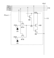
単位画素102の各々は、例えば図2に示す回路によって構成され得る。すなわち、単位画素102の各々は、図2に示すように、フォトダイオードPDA,PDBと、転送トランジスタM1A,M1Bと、リセットトランジスタM2と、増幅トランジスタM3と、選択トランジスタM4と、を含み得る。
Each
フォトダイオードPDA,PDBは、前述の光電変換部102A,102Bに対応している。1つの単位画素102のフォトダイオードPDA,PDBは、1つのマイクロレンズ(図示せず)を共有し、撮像レンズの射出瞳の異なる瞳領域を通過した光が入射するように構成されている。これにより、フォトダイオードPDAで生じた電荷に基づく信号と、フォトダイオードPDBで生じた電荷に基づく信号とを、焦点距離検出用の信号として使用することができる。また、フォトダイオードPDAで生じた電荷とフォトダイオードPDBで生じた電荷とを加えた総電荷に基づく信号は、画像取得用の信号として使用することができる。
The photodiodes PDA and PDB correspond to the
フォトダイオードPDAは、アノードが接地ノード(GND)に接続され、カソードが転送トランジスタM1Aのソースに接続されている。フォトダイオードPDBは、アノードが接地ノード(GND)に接続され、カソードが転送トランジスタM1Bのソースに接続されている。転送トランジスタM1A,M1Bのドレインは、リセットトランジスタM2のソース及び増幅トランジスタM3のゲートに接続されている。転送トランジスタM1A,M1Bのドレイン、リセットトランジスタM2のソース及び増幅トランジスタM3のゲートの接続ノードは、いわゆるフローティングディフュージョンFDである。フローティングディフュージョンFDは、容量成分を含み、電荷保持部として機能するとともに、この容量成分からなる電荷電圧変換部を構成する。リセットトランジスタM2のドレイン及び増幅トランジスタM3のドレインは、電源ノード(電圧VDD)に接続されている。増幅トランジスタM3のソースは、選択トランジスタM4のドレインに接続されている。選択トランジスタM4のソースは、垂直出力線111に接続されている。なお、トランジスタのソースとドレインの呼称は、トランジスタの導電型や着目する機能等に応じて異なることがあり、上述のソースとドレインとは逆の名称で呼ばれることもある。
The photodiode PDA has an anode connected to the ground node (GND) and a cathode connected to the source of the transfer transistor M1A. The photodiode PDB has an anode connected to the ground node (GND) and a cathode connected to the source of the transfer transistor M1B. The drains of the transfer transistors M1A and M1B are connected to the source of the reset transistor M2 and the gate of the amplification transistor M3. A connection node of the drains of the transfer transistors M1A and M1B, the source of the reset transistor M2, and the gate of the amplification transistor M3 is a so-called floating diffusion FD. The floating diffusion FD includes a capacitive component, functions as a charge holding section, and constitutes a charge-voltage converting section composed of this capacitive component. A drain of the reset transistor M2 and a drain of the amplification transistor M3 are connected to a power supply node (voltage VDD). The source of the amplification transistor M3 is connected to the drain of the selection transistor M4. The source of the selection transistor M4 is connected to the
各行の行選択線110は、転送トランジスタM1Aのゲートに接続された信号線と、転送トランジスタM1Bのゲートに接続された信号線と、リセットトランジスタM2のゲートに接続された信号線と、選択トランジスタM4のゲートに接続された信号線とを含む。転送トランジスタM1Aのゲートに接続された信号線には、垂直走査部103から、制御信号PTXAが供給される。転送トランジスタM1Bのゲートに接続された信号線には、垂直走査部103から、制御信号PTXBが供給される。リセットトランジスタM2のゲートに接続された信号線には、垂直走査部103から、制御信号PRESが供給される。選択トランジスタM4のゲートに接続された信号線には、垂直走査部103から、制御信号PSELが供給される。各トランジスタがN型トランジスタで構成される場合、垂直走査部103からハイレベルの制御信号が供給されると対応するトランジスタがオンとなり、垂直走査部103からローレベルの制御信号が供給されると対応するトランジスタがオフとなる。
The
画素部101に光が入射すると、各単位画素102のフォトダイオードPDA,PDBは、入射光をその光量に応じた量の電荷に変換(光電変換)するとともに、生じた電荷を蓄積する。転送トランジスタM1A,M1Bは、オンすることによりフォトダイオードPDA,PDBの電荷をフローティングディフュージョンFDに転送する。フローティングディフュージョンFDは、フォトダイオードPDA,PDBから転送された電荷を保持する。A像信号を読み出す際は、フォトダイオードPDAにて光電変換された電荷のみが転送トランジスタM1Aを介してフローティングディフュージョンFDに転送される。B像信号を読み出す際は、フォトダイオードPDBにて光電変換された電荷のみが転送トランジスタM1Bを介してフローティングディフュージョンFDに転送される。A+B像信号を読み出す際は、フォトダイオードPDA,PDBにて光電変換された総電荷が転送トランジスタM1A,M1Bを介してフローティングディフュージョンFDに転送される。これにより、フローティングディフュージョンFDは、その容量成分による電荷電圧変換によって、フォトダイオードPDA,PDBから転送された電荷の量に応じた電圧となる。
When light enters the
増幅トランジスタM3は、ドレインに電圧VDDが供給され、ソースに選択トランジスタM4を介して図示しない電流源からバイアス電流が供給される構成となっており、ゲートを入力ノードとする増幅部(ソースフォロワ回路)を構成する。これにより増幅トランジスタM3は、フローティングディフュージョンFDの電圧に基づく信号を、選択トランジスタM4を介して垂直出力線111に出力する。リセットトランジスタM2は、オンすることによりフローティングディフュージョンFDを電圧VDDに応じた電圧にリセットする。
The amplification transistor M3 has a drain supplied with the voltage VDD and a source supplied with a bias current from a current source (not shown) via the selection transistor M4. ). As a result, the amplification transistor M3 outputs a signal based on the voltage of the floating diffusion FD to the
単位画素102の転送トランジスタM1A,M1B、リセットトランジスタM2及び選択トランジスタM4は、垂直走査部103から供給される制御信号PTXA,PTXB,PRES,PSELにより、行単位で制御される。制御信号PSELにより選択された行(選択行)に属する複数の単位画素102の画素信号は、各列の垂直出力線111に同時に出力される。
The transfer transistors M1A, M1B, the reset transistor M2, and the selection transistor M4 of the
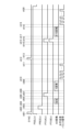
次に、本実施形態による撮像装置の画素部101の動作について、図3及び図4を用いて説明する。図3は、撮像画像用データ行に属する単位画素102から画素信号を読み出す場合のタイミングチャートである。図4は、焦点検出用データ行に属する単位画素102から画素信号の読み出す場合のタイミングチャートである。図3及び図4には一例として、垂直走査部103によってn行目の単位画素102が選択された際の読み出し動作を示している。なお、単位画素102の各トランジスタは、垂直走査部103からHighレベルの制御信号が供給されるとオンになり、垂直走査部103からLowレベルの制御信号が供給されるとオフになるものとする。
Next, the operation of the
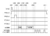
まず、撮像画像用データ行に対する読み出し動作について、図3を用いて説明する。図3には、水平同期信号SYNC、制御信号PSEL(n),PRES(n),PTXA(n),PTXB(n)、AD変換の期間、水平走査パルス信号を示している。 First, the readout operation for the captured image data row will be described with reference to FIG. FIG. 3 shows the horizontal synchronization signal SYNC, the control signals PSEL(n), PRES(n), PTXA(n), PTXB(n), AD conversion period, and horizontal scanning pulse signal.
撮像画像用データ行からのデータの読み出しは、フォトダイオードPDA,PDBで生成された電荷を合成することによって得られる合成電荷に応じた信号のみを読み出す駆動モードで行われる。 Data reading from the captured image data row is performed in a driving mode in which only a signal corresponding to the combined charge obtained by combining the charges generated by the photodiodes PDA and PDB is read.
時刻t301において、TG部104から垂直走査部103に供給される水平同期信号SYNCがLowレベルからHighレベルへと遷移する。この水平同期信号SYNCの立ち上がりに応じて、垂直走査部103は、第n行の制御信号PSEL(n)をLowレベルからHighレベルへと制御する。これにより、第n行に属する単位画素102は、選択トランジスタM4がオン状態となり、選択トランジスタM4を介して垂直出力線111に画素信号を出力可能な状態となる。すなわち、垂直走査部103からの制御信号PSEL(n)によって第n行が選択される。
At time t301, the horizontal synchronization signal SYNC supplied from the
続く時刻t302において、垂直走査部103は、選択された行、すなわち第n行の制御信号PRES(n)をLowレベルからHighレベルへと制御する。これにより、第n行に属する単位画素102は、リセットトランジスタM2がオン状態となり、フローティングディフュージョンFDが電圧VDDに応じた電位にリセットされる。
At subsequent time t302, the
続く時刻t303において、垂直走査部103は、第n行の制御信号PRES(n)をHighレベルからLowレベルへと制御する。これにより、第n行に属する単位画素102は、リセットトランジスタM2がオフ状態となり、フローティングディフュージョンFDのリセットが解除される。このとき、第n行に属する単位画素102の選択トランジスタM4はオン状態のままであるため、フローティングディフュージョンFDのリセットが解除された際の増幅トランジスタM3のゲートの電位に応じた出力信号が、垂直出力線111に出力される。このようにして単位画素102から出力されるリセットレベルの画素信号を、N信号(ノイズ信号)と称することとする。
At subsequent time t303, the
続く時刻t304から時刻t305の期間は、垂直出力線111に出力されたN信号に対してAD変換処理を行う期間である。垂直出力線111に出力されたN信号は、読み出し回路部105に読み出され、AD変換部106でデジタル信号に変換される。AD変換部106によって得られたN信号のデジタル信号は、メモリ部107に保持される。時刻t304から時刻t305において行われる動作、すなわちN信号をデジタル信号に変換する動作を、N変換と称することとする。
A period from time t304 to time t305 is a period in which the N signal output to the
続く時刻t306において、垂直走査部103は、第n行の制御信号PTXA(n),PTXB(n)をそれぞれLowレベルからHighレベルへと制御する。これにより、第n行に属する単位画素102は、転送トランジスタM1A,M1Bがオン状態となり、フォトダイオードPDA,PDBに蓄積されていた電荷がフローティングディフュージョンFDに転送される。これにより、フローティングディフュージョンFD、すなわち増幅トランジスタM3のゲートの電位が、フォトダイオードPDA,PDBから転送された電荷の量に応じた電位となる。このとき、第n行に属する単位画素102の選択トランジスタM4はオン状態のままであるため、垂直出力線111には、フォトダイオードPDA,PDBで発生した電荷の総量に応じた画素信号であるA+B像信号が出力される。
At subsequent time t306, the
続く時刻t307において、垂直走査部103は、第n行の制御信号PTXA(n),PTXB(n)をそれぞれHighレベルからLowレベルへと制御する。これにより、第n行に属する単位画素102の転送トランジスタM1A,M1Bがオフ状態となる。転送トランジスタM1A,M1Bがオフ状態となった後も、垂直出力線111にはA+B像信号が出力され続ける。
At subsequent time t307, the
続く時刻t308から時刻t309の期間は、垂直出力線111に出力されたA+B像信号に対してAD変換処理を行う期間である。垂直出力線111に出力されたA+B像信号は、読み出し回路部105に読み出され、AD変換部106でデジタル信号に変換される。AD変換部106によって得られたA+B像信号のデジタル信号は、メモリ部107のN信号が保持されたメモリとは異なるメモリに保持される。時刻t308から時刻t309において行われる動作、すなわちA+B像信号をデジタル信号に変換する動作を、A+B変換と称することとする。
A period from time t308 to time t309 is a period in which AD conversion processing is performed on the A+B image signal output to the
続く時刻t310から時刻t311の期間は、メモリ部107に保持されたN信号及びA+B像信号を信号処理部109へと転送する期間である。水平走査部108は、メモリ部107に水平走査パルス信号を出力する。メモリ部107は、水平走査パルス信号で選択されたアドレス(列)に対応するN信号及びA+B像信号を信号処理部109へと転送する。この動作を水平走査パルス信号が選択するアドレスを変えながら第0列から第m列まで繰り返し行う(水平走査を行う)ことにより、読み出し対象となっている行の1行分のN信号とA+B像信号とを読み出すことができる。信号処理部109は、A+B像信号から当該A+B像信号に対応するN信号を減算する処理を行い、A+B像信号に重畳する固定パターンノイズを除去する。
A period from time t310 to time t311 is a period during which the N signal and the A+B image signal held in the
その後、垂直走査部103は、第n行の制御信号PSEL(n)をHighレベルからLowレベルへと制御して第n行の選択を解除し、撮像画像用データ行の1行分の読み出し動作を完了し、次の行の読み出し動作へと移行する。
After that, the
次に、焦点検出用データ行に対する読み出し動作について、図4を用いて説明する。図4には、水平同期信号SYNC、制御信号PSEL(n),PRES(n),PTXA(n),PTXB(n)、AD変換の期間、水平走査パルス信号を示している。 Next, the readout operation for the focus detection data row will be described with reference to FIG. FIG. 4 shows the horizontal synchronizing signal SYNC, the control signals PSEL(n), PRES(n), PTXA(n), PTXB(n), the AD conversion period, and the horizontal scanning pulse signal.
焦点検出用データ行からの読み出しは、フォトダイオードPDAで生成された電荷に応じた信号と、フォトダイオードPDA,PDBで生成された電荷を合成することによって得られる合成電荷に応じた信号と、を読み出す駆動モードで行われる。 For reading from the focus detection data row, a signal corresponding to the charge generated by the photodiode PDA and a signal corresponding to the combined charge obtained by synthesizing the charges generated by the photodiodes PDA and PDB are used. This is done in read drive mode.
時刻t401において、TG部104から垂直走査部103に供給される水平同期信号SYNCがLowレベルからHighレベルへと遷移する。この水平同期信号SYNCの立ち上がりに応じて、垂直走査部103は、第n行の制御信号PSEL(n)をLowレベルからHighレベルへと制御する。これにより、第n行に属する単位画素102の選択トランジスタM4がオン状態となり、第n行が選択される。
At time t401, the horizontal synchronization signal SYNC supplied from the
続く時刻t402において、垂直走査部103は、第n行の制御信号PRES(n)をLowレベルからHighレベルへと制御する。これにより、第n行に属する単位画素102は、リセットトランジスタM2がオン状態となり、フローティングディフュージョンFDが電圧VDDに応じた電位にリセットされる。
At subsequent time t402, the
続く時刻t403において、垂直走査部103は、第n行の制御信号PRES(n)をHighレベルからLowレベルへと制御する。これにより、第n行に属する単位画素102は、リセットトランジスタM2がオフ状態となり、フローティングディフュージョンFDのリセットが解除される。このとき、第n行に属する単位画素102の選択トランジスタM4はオン状態のままであるため、リセットレベルの画素信号(N信号)が垂直出力線111に出力される。
At subsequent time t403, the
続く時刻t404から時刻t405の期間は、垂直出力線111に出力されたN信号に対してAD変換処理(N変換)を行う期間である。垂直出力線111に出力されたN信号は、読み出し回路部105に読み出され、AD変換部106でデジタル信号に変換される。AD変換部106によって得られたN信号のデジタル信号は、メモリ部107に保持される。
A period from time t404 to time t405 is a period in which the N signal output to the
続く時刻t406において、垂直走査部103は、第n行の制御信号PTXA(n)をLowレベルからHighレベルへと制御する。これにより、第n行に属する単位画素102は、転送トランジスタM1Aがオン状態となり、フォトダイオードPDAに蓄積されていた電荷がフローティングディフュージョンFDに転送される。これにより、フローティングディフュージョンFD、すなわち増幅トランジスタM3のゲートの電位が、フォトダイオードPDAから転送された電荷の量に応じた電位となる。このとき、第n行に属する単位画素102の選択トランジスタM4はオン状態のままであるため、垂直出力線111には、フォトダイオードPDAで発生した電荷の量に応じた画素信号であるA像信号が出力される。
At subsequent time t406, the
続く時刻t407において、垂直走査部103は、第n行の制御信号PTXA(n)をHighレベルからLowレベルへと制御する。これにより、第n行に属する単位画素102の転送トランジスタM1Aがオフ状態となる。転送トランジスタM1Aがオフ状態となった後も、垂直出力線111にはA像信号が出力され続ける。
At subsequent time t407, the
続く時刻t408から時刻t409の期間は、垂直出力線111に出力されたA像信号に対してAD変換処理を行う期間である。垂直出力線111に出力されたA像信号は、読み出し回路部105に読み出され、AD変換部106でデジタル信号に変換される。AD変換部106によって得られたA像信号のデジタル信号は、メモリ部107のN信号が保持されたメモリとは異なるメモリに保持される。時刻t408から時刻t409において行われる動作、すなわちA像信号をデジタル信号に変換する動作を、A変換と称することとする。
A period from time t408 to time t409 is a period in which AD conversion processing is performed on the A image signal output to the
続く時刻t410から時刻t411の期間は、メモリ部107に保持されたN信号及びA像信号を信号処理部109へと転送する期間である。水平走査部108は、メモリ部107に水平走査パルス信号を出力する。メモリ部107は、水平走査パルス信号で選択されたアドレス(列)に対応するN信号及びA像信号を信号処理部109へと転送する。この動作を水平走査パルス信号が選択するアドレスを変えながら第0列から第m列まで繰り返し行う(水平走査を行う)ことにより、読み出し対象となっている行の1行分のN信号とA像信号とを読み出すことができる。
A period from time t410 to time t411 is a period during which the N signal and the A image signal held in the
続く時刻t412において、TG部104から垂直走査部103に供給される水平同期信号SYNCが、再びLowレベルからHighレベルへと遷移する。このとき、第n行に属する単位画素102の選択トランジスタM4はオン状態のままであり、第n行が選択された状態が維持される。
At subsequent time t412, the horizontal synchronization signal SYNC supplied from the
続く時刻t413から時刻t414の期間において、垂直走査部103は、第n行の制御信号PRES(n)をLowレベルのまま維持する。すなわち、時刻t413から時刻t414の期間では、フローティングディフュージョンFDのリセット及びN変換を実施しない。フローティングディフュージョンFDには、時刻t406から時刻407の期間の間にフォトダイオードPDAから転送された電荷がそのまま保持された状態である。
During the subsequent period from time t413 to time t414, the
続く時刻t415において、垂直走査部103は、第n行の制御信号PTXA(n),PTXB(n)をLowレベルからHighレベルへと制御する。これにより、第n行に属する単位画素102は、転送トランジスタM1A,M1Bがオン状態となり、フォトダイオードPDBに蓄積されていた電荷がフローティングディフュージョンFDに転送される。これにより、フローティングディフュージョンFDでは、フォトダイオードPDAから転送された電荷に、フォトダイオードPDBから転送された電荷が加算される。フローティングディフュージョンFDの電位、すなわち増幅トランジスタM3のゲートの電位は、フォトダイオードPDA,PDBから転送された電荷の総量に応じた電位となる。このとき、第n行に属する単位画素102の選択トランジスタM4はオン状態のままであるため、垂直出力線111には、フォトダイオードPDA,PDBで発生した電荷の総量に応じた画素信号であるA+B像信号が出力される。
At subsequent time t415, the
続く時刻t416において、垂直走査部103は、第n行の制御信号PTXA(n),PTXB(n)をHighレベルからLowレベルへと制御する。これにより、第n行に属する単位画素102の転送トランジスタM1A,M1Bがオフ状態となる。転送トランジスタM1A,M1Bがオフ状態となった後も、垂直出力線111にはA+B像信号が出力され続ける。
At subsequent time t416, the
続く時刻t417から時刻t418の期間は、垂直出力線111に出力されたA+B像信号に対してAD変換処理(A+B変換)を行う期間である。垂直出力線111に出力されたA+B像信号は、読み出し回路部105に読み出され、AD変換部106でデジタル信号に変換される。AD変換部106によって得られたA+B像信号のデジタル信号は、メモリ部107のA像信号を保持していたメモリと同じメモリに保持される。
A period from time t417 to time t418 is a period in which AD conversion processing (A+B conversion) is performed on the A+B image signals output to the
続く時刻t419から時刻t420の期間は、メモリ部107に保持されたN信号及びA+B像信号を信号処理部109へと転送する期間である。水平走査部108は、メモリ部107に水平走査パルス信号を出力する。メモリ部107は、水平走査パルス信号で選択されたアドレス(列)に対応するN信号及びA+B像信号を信号処理部109へと転送する。この動作を水平走査パルス信号が選択するアドレスを変えながら第0列から第m列まで繰り返し行う(水平走査を行う)ことにより、読み出し対象となっている行の1行分のN信号とA+B像信号とを読み出すことができる。
A period from time t419 to time t420 is a period during which the N signal and the A+B image signal held in the
このようにして、読み出し対象となっている行の1行分のA像信号と、当該A像信号に対応するN信号と、A+B像信号と、当該A+B像信号に対応するN信号と、を読み出すことができる。 In this way, the A image signal for one row of the read target row, the N signal corresponding to the A image signal, the A+B image signal, and the N signal corresponding to the A+B image signal are obtained. can be read.
信号処理部109は、A像信号から当該A像信号に対応するN信号を減算する処理を行い、A像信号に重畳する固定パターンノイズを除去する。また、信号処理部109は、A+B像信号から当該A+B像信号に対応するN信号を減算する処理を行い、A+B像信号に重畳する固定パターンノイズを除去する。焦点検出を行うために必要となるB像信号は、A+B像信号からA像信号を減算することによって得ることができる。
The
その後、垂直走査部103は、第n行の制御信号PSEL(n)をHighレベルからLowレベルへと制御して第n行の選択を解除し、焦点検出用データ行の1行分の読み出し動作を完了し、次の行の読み出し動作へと移行する。
After that, the
撮像画像用データ行の単位画素102から画素信号を読み出す際には、図3に示したように、A+B像信号を読み出す。一方、焦点検出用データ行の単位画素102から画素信号を読み出す際には、図4に示すように、同じ行からA像信号とA+B像信号とを読み出す。そのため、上記駆動方法によれば、画素部101を構成する総ての行からA像信号とB像信号とを読み出す場合に比べて、読み出し時間を短縮することが可能となる。
When reading the pixel signal from the
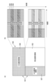
図5は、本実施形態の撮像装置における読み出し動作を概念的に説明する図である。図5(a)は、画素部101に配される画素アレイ500の構成例を示している。図5(b)は、撮像装置100から出力される信号を、水平同期信号SYNCを基準に改行しながら、出力される順番で左から順に並べた概念図である。図5(b)における水平方向の幅が、水平同期信号SYNCの間隔で規定される1水平期間の長さに対応している。
FIG. 5 is a diagram conceptually explaining the readout operation in the imaging apparatus of this embodiment. FIG. 5A shows a configuration example of a
画素部101を構成する複数の単位画素102は、フォトダイオードPDA,PDBが遮光されていない受光画素と、フォトダイオードPDA,PDBが遮光されたオプティカルブラック(OB)画素と、を含む画素アレイ500を構成する。画素アレイ500のうち、受光画素が配された領域が受光画素領域502であり、OB画素が配された領域が基準画素領域(OB画素領域とも言う)501である。図5では、基準画素領域501と受光画素領域502とを視覚的に区別しやすいように、基準画素領域501にドットパターンを付している。基準画素領域501には、任意の領域を設定することができ、設定した領域は受光画素の出力データに対する補正処理において用いられる補正値(クランプ値)を生成するために使用することができる。この領域をクランプ値取得領域と称することとする。
A plurality of
ここでは、基準画素領域501のうち、画素部101の上側の辺に接する領域をVOB画素領域506と称し、画素部101の左側の辺に接する領域をHOB画素領域507と称することとする。VOB画素領域506は、受光画素領域502の受光画素が配された行とは異なる行に配されたOB画素を含む領域である。HOB画素領域507は、受光画素領域502の受光画素が配された行と同じ行の異なる列に配されたOB画素を含む領域である。一例では、クランプ値取得領域は、VOB画素領域506のうちの一部の行に設定される。
Here, of the
図5(b)は、画素アレイ500から読み出された画素信号の内訳を示している。図5(b)では、撮像画像用データ行から読み出したデータと焦点検出用データ行から読み出したデータとを視覚的に区別しやすいように、焦点検出用データ行から読み出したデータに線影を付している。例えば、画素アレイ500のある撮像画像用データ行からは、図3のタイミングチャートに従って、水平期間503の間にA+B像信号が出力される。また、画素アレイ500のある焦点検出用データ行からは、図4のタイミングチャートに従って、水平期間504の間にA像信号が出力され、次の水平期間505の間にA+B像信号が出力される。
FIG. 5B shows the breakdown of pixel signals read out from the
このように、本実施形態による撮像装置の読み出し動作では、撮像画像用データの出力中に焦点検出用データが離散的に出力される。 As described above, in the readout operation of the imaging apparatus according to the present embodiment, the focus detection data is discretely output while the captured image data is being output.
次に、信号処理部109において行われる信号処理について説明する。信号処理部109では、まず、A+B像信号から当該A+B像信号に対応するN信号を減算する処理が行われる。これにより、A+B像信号から固定パターンノイズが除去される。次に、固定パターンノイズを除去したA+B像信号から、基準画素領域501に配された単位画素102の出力信号から生成されたクランプ値を減算する処理が行われる。この処理は、黒レベルを基準レベルに合わせる補正処理である。
Next, signal processing performed in the
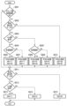
図6は、本実施形態の撮像装置におけるクランプ値の生成方法を示すフローチャートである。クランプ値を生成する際は、画素部101から出力されるデータ群から順次データを取り込み、単位画素102の各々から出力されるデータに対して、図6に示すフローチャートに従った処理を行う。単位画素102の各々に対するクランプ値は、図6に示すステップS601からステップS615に従って生成される。
FIG. 6 is a flow chart showing a clamp value generation method in the imaging apparatus of this embodiment. When generating the clamp value, data is sequentially captured from the data group output from the
まず、ステップS601において、対象データがクランプ値取得領域内のデータであるか否かを判別する。判別の結果、対象データがクランプ値取得領域内のデータである場合(Yes)にはステップS602に移行し、対象データがクランプ値取得領域内のデータではない場合(No)にはステップS611に移行する。 First, in step S601, it is determined whether or not the target data is data within the clamp value acquisition area. As a result of determination, if the target data is data within the clamp value acquisition area (Yes), the process proceeds to step S602, and if the target data is not data within the clamp value acquisition area (No), the process proceeds to step S611. do.
ステップS602では、対象データが焦点検出用データ行のデータであるか否かを判別する。判別の結果、対象データが焦点検出用データ行のデータである場合(Yes)にはステップS603に移行し、対象データが焦点検出用データ行のデータではない場合(No)にはステップS610に移行する。 In step S602, it is determined whether or not the target data is the data of the focus detection data row. As a result of determination, if the target data is the data of the data line for focus detection (Yes), the process proceeds to step S603, and if the target data is not the data of the data line for focus detection (No), the process proceeds to step S610. do.
ステップS603では、対象データが焦点検出用データ行のA+B像信号であるかA像信号であるかを判別する。判別の結果、対象データが焦点検出用データ行のA+B像信号である場合(Yes)にはステップS604に移行し、対象データが焦点検出用データ行のA像信号である場合(No)にはステップS605に移行する。 In step S603, it is determined whether the target data is the A+B image signal or the A image signal of the focus detection data row. As a result of determination, if the target data is the A+B image signal of the focus detection data row (Yes), the process proceeds to step S604, and if the target data is the A image signal of the focus detection data row (No), The process proceeds to step S605.
ステップS604では、対象データが焦点検出用データ行の先頭画素のA+B像信号であるか否かを判別する。ここで、先頭画素とは、クランプ値取得領域の各行において最初に処理する画素のことである。判別の結果、対象データが焦点検出用データ行の先頭画素のA+B像信号である場合(Yes)にはステップS606に移行し、対象データが焦点検出用データ行の先頭画素のA+B像信号ではない場合(No)にはステップS607に移行する。 In step S604, it is determined whether or not the target data is the A+B image signal of the top pixel of the focus detection data row. Here, the top pixel is the first pixel to be processed in each row of the clamp value acquisition area. As a result of determination, if the target data is the A+B image signal of the top pixel of the focus detection data row (Yes), the process proceeds to step S606, and the target data is not the A+B image signal of the top pixel of the focus detection data row. In the case (No), the process proceeds to step S607.
ステップS605では、対象のデータが焦点検出用データ行の先頭画素のA像信号であるか否かを判別する。判別の結果、対象データが焦点検出用データ行の先頭画素のA像信号である場合(Yes)にはステップS608に移行し、対象データが焦点検出用データ行の先頭画素のA像信号ではない場合(No)にはステップS609に移行する。 In step S605, it is determined whether or not the target data is the A image signal of the top pixel of the focus detection data row. As a result of determination, if the target data is the A image signal of the top pixel of the focus detection data row (Yes), the process proceeds to step S608, and the target data is not the A image signal of the top pixel of the focus detection data row. In the case (No), the process proceeds to step S609.
ステップS606~S610では、対象データの種類に応じた平均化処理を行う。対象データの平均化処理には、例えば図7に示すLPF(Low Pass Filter)回路が用いられる。図7は、本実施形態においてクランプ値の生成に用いるLPF回路の構成例を示すブロック図である。 In steps S606 to S610, averaging processing is performed according to the type of target data. An LPF (Low Pass Filter) circuit shown in FIG. 7, for example, is used for averaging the target data. FIG. 7 is a block diagram showing a configuration example of an LPF circuit used for generating clamp values in this embodiment.
本実施形態においてクランプ値の生成に用いるLPF回路は、図7に示すように、平均化回路700と、保持部704,705,706と、スイッチ707,708,709と、を有する。平均化回路700は、減算部701と、減衰部702と、加算部703と、を有する。
The LPF circuit used to generate the clamp value in this embodiment has an averaging
平均化回路700は、減算部701にて入力データと保持データとの差分を算出し、減衰部702にて差分データを所定のフィードバックゲインに従って減衰し、加算部703にて減衰データと保持データとを加算し、保持部704,705,706に保持する。平均化回路700は、データが入力される都度この処理を実行し、目標レベル、すなわち入力データの平均値との差分データを少しずつ加算していくことによって保持データを目標レベルに漸近させる。
Averaging
i行目のクランプ値OBC(i)を求める伝達関数は、以下の通りである。
OBC(i)=OBC(i-1)
+(Darklevel-OBC(i-1))×ATT
ここで、Darklevelは基準画素領域501から取得する基準黒レベルを示し、ATTはフィードバックゲインを示す。
A transfer function for obtaining the i-th clamp value OBC(i) is as follows.
OBC(i) = OBC(i-1)
+ (Darklevel - OBC (i - 1)) x ATT
Here, Darklevel indicates the reference black level obtained from the
保持部704,705,706は、クランプ値を保持するための保持部である。具体的には、保持部704は、撮像画像用データ行用のクランプ値を保持するための保持部である。保持部705は、焦点検出用データ行のA像信号用のクランプ値を保持するための保持部である。保持部706は、焦点検出用データ行のA+B像信号用のクランプ値を保持するための保持部である。
Holding
スイッチ707,708,709は、保持部704,705,706を選択するスイッチである。具体的には、スイッチ707は、平均化回路700により処理したデータを保持部704,705,706のうちのどの保持部に保持するのかを切り替えるスイッチである。スイッチ708は、平均化回路700で平均化処理をする際のフィードバックデータとして、保持部704,705,706のうちのどの保持部に保持されたクランプ値を用いるのかを切り替えるスイッチである。スイッチ709は、クランプ値として、保持部704,705,706のうちのどの保持部に保持されたデータを用いるのかを切り替えるスイッチである。
減算部701は、入力データINと、保持部704,705,706が保持する保持データのうちスイッチ708で選択された保持部に保持された保持データとの差分を算出し、減衰部702に差分データを出力する。スイッチ708は、制御信号SW2の値に応じて、保持部704,705,706のうちのいずれかを選択する。減衰部702は、差分データを所定のフィードバックゲインに従って減衰し、加算部703に減衰データを出力する。加算部703は、減衰データとスイッチ708で選択された保持データとを加算し、保持部704,705,706のうちスイッチ707で選択された保持部に、加算データを新たな保持データとして保持する。スイッチ707は、制御信号SW1の値に応じて、保持部704,705,706のうちのいずれかを選択する。スイッチ709は、制御信号SW3の値に応じて、保持部704,705,706が保持する保持データのうちのいずれかを選択し、出力データOUTとして出力する。この出力データOUTが、補正処理に用いられるクランプ値となる。
ステップS610では、撮像画像用データ行の画素データに対して、SW1=00,SW2=00として平均化処理を実施する。すなわち、対象データがクランプ値取得領域の撮像画像用データ行のデータであるときは、保持部704に保持された撮像画像用データ行用のクランプ値をフィードバックデータとしてクランプ値を生成し、保持部704に保持する。ステップS610の処理後は、ステップS611に移行する。
In step S610, averaging processing is performed on the pixel data of the captured image data row with SW1=00 and SW2=00. That is, when the target data is the data of the captured image data row in the clamp value acquisition area, the clamp value is generated using the clamp value for the captured image data row held in the holding
ステップS606では、焦点検出用データ行の先頭画素のA+B像信号に対して、SW1=11,SW2=00として平均化処理を実施する。すなわち、焦点検出用データ行の先頭画素のA+B像信号を処理する際は、保持部704に保持された撮像画像用データ行用のクランプ値をフィードバックデータとしてクランプ値を生成し、保持部706に保持する。つまり、撮像画像用データ行用のクランプ値を初期値としてA+B像信号に対するクランプ値を生成する。ステップS606の処理後は、ステップS611に移行する。
In step S606, averaging processing is performed with SW1=11 and SW2=00 on the A+B image signals of the top pixel of the focus detection data row. That is, when processing the A+B image signal of the leading pixel of the focus detection data row, the clamp value for the captured image data row held in the holding
ステップS607では、焦点検出用データ行の先頭画素以外の画素のA+B像信号に対して、SW1=11,SW2=11として平均化処理を実施する。すなわち、焦点検出用データ行の先頭画素以外の画素のA+B像信号を処理する際は、保持部706に保持された焦点検出用データ行のA+B像信号用のクランプ値をフィードバックデータとしてクランプ値を生成し、保持部706に保持する。ステップS607の処理後は、ステップS611に移行する。
In step S607, averaging processing is performed with SW1=11 and SW2=11 for the A+B image signals of pixels other than the first pixel of the focus detection data row. That is, when processing the A+B image signals of pixels other than the first pixel of the focus detection data row, the clamp value for the A+B image signals of the focus detection data row held in the holding
ステップS608では、焦点検出用データ行の先頭画素のA像信号に対して、SW1=01,SW2=00として平均化処理を実施する。すなわち、焦点検出用データ行の先頭画素のA像信号を処理する際は、保持部704に保持された撮像画像用データ行用のクランプ値をフィードバックデータとしてクランプ値を生成し、保持部705に保持する。つまり、撮像画像用データ行用のクランプ値を初期値としてA像信号に対するクランプ値を生成する。ステップS608の処理後は、ステップS611に移行する。
In step S608, averaging processing is performed with SW1=01 and SW2=00 on the A image signal of the top pixel of the data row for focus detection. That is, when processing the A image signal of the leading pixel of the focus detection data row, the clamp value for the captured image data row held in the holding
ステップS609では、焦点検出用データ行の先頭画素以外の画素のA像信号に対して、SW1=01,SW2=01として平均化処理を実施する。すなわち、焦点検出用データ行の先頭画素以外の画素のA像信号を処理する際は、保持部705に保持された焦点検出用データ行のA像信号用のクランプ値をフィードバックデータとしてクランプ値を生成し、保持部705に保持する。ステップS609の処理後は、ステップS611に移行する。
In step S609, averaging processing is performed with SW1=01 and SW2=01 for the A image signals of the pixels other than the top pixel of the focus detection data row. That is, when processing the A image signal of pixels other than the first pixel of the focus detection data row, the clamp value for the A image signal of the focus detection data row held in the holding
ステップS611では、対象データが焦点検出用データ行のデータであるか否かを判別する。判別の結果、対象データが焦点検出用データ行のデータである場合(Yes)にはステップS612に移行し、対象データが焦点検出用データ行のデータではない場合(No)にはステップS615に移行する。 In step S611, it is determined whether or not the target data is the data of the focus detection data row. As a result of determination, if the target data is the data of the focus detection data line (Yes), the process proceeds to step S612, and if the target data is not the data of the focus detection data line (No), the process proceeds to step S615. do.
ステップS612では、対象データが焦点検出用データ行のうちのA+B像信号であるかA像信号であるかを判別する。判別の結果、対象データが焦点検出用データ行のA+B像信号である場合(Yes)にはステップS613に移行し、対象データが焦点検出用データ行のA像信号である場合(No)にはステップS614に移行する。 In step S612, it is determined whether the target data is the A+B image signal or the A image signal in the focus detection data row. As a result of determination, if the target data is the A+B image signal of the focus detection data row (Yes), the process proceeds to step S613, and if the target data is the A image signal of the focus detection data row (No), The process proceeds to step S614.
ステップS613では、制御信号SW3をSW3=11として、LPF回路の出力端子に焦点検出用データ行のA+B像信号用の保持部706を接続する。すなわち、黒レベル補正処理を行う際には、保持部706に保持されている焦点検出用データ行のA+B像信号用のクランプ値を用いる。
In step S613, the control signal SW3 is set to SW3=11, and the holding
ステップS614では、制御信号SW3をSW3=01として、平均化回路700の出力端子に焦点検出用データ行のA像信号用の保持部705を接続する。すなわち、黒レベル補正処理を行う際には、保持部705に保持されている焦点検出用データ行のA像信号用のクランプ値を用いる。
In step S614, the control signal SW3 is set to SW3=01, and the output terminal of the averaging
ステップS615では、制御信号SW3をSW3=00として、平均化回路700の出力端子に撮像画像用データ行用の保持部704を接続する。すなわち、黒レベル補正処理を行う際には、保持部704に保持されている撮像画像用データ行用のクランプ値を用いる。
In step S615, the control signal SW3 is set to SW3=00, and the holding
本実施形態による撮像装置の効果について、図20を用いて説明する。図20は、本実施形態による撮像装置の効果を説明する概略図である。図20(a)は、VOB画素領域506に属する行の一部を抜き出した概略図である。図20(b)は、図20(a)の対応する行における信号レベルを示している。図20(b)において、縦軸は時間を表し、横軸は信号レベルを表している。
Effects of the imaging device according to this embodiment will be described with reference to FIG. 20 . FIG. 20 is a schematic diagram for explaining the effect of the imaging device according to this embodiment. FIG. 20(a) is a schematic diagram of a part of a row belonging to the
図20では、VOB画素領域506において、垂直方向に基準黒レベルが増加していくシェーディングが生じている場合を想定している。例えば、図20(b)の最上部に示す撮像画像用データ行における基準黒レベルは信号レベルL1であり、図20(b)の最下部に示す撮像画像用データ行における基準黒レベルは信号レベルL5である。信号レベルL1と信号レベルL5との間のこの信号レベル差が、垂直方向にシェーディングが生じていることを表している。
In FIG. 20, it is assumed that shading occurs in the
本実施形態の適用例として、垂直方向のシェーディングに追従した撮像画像用データ行用のクランプ値を、図20に直線2001として表している。本実施形態のLPF回路を用いることで、撮像画像用データ行のクランプ値を垂直方向のシェーディングに追従させることができる。これにより、垂直方向のシェーディングに追従した黒レベル補正が可能となる。
As an application example of this embodiment, the clamp value for the captured image data row that follows the shading in the vertical direction is represented as a
信号レベルL3は、信号レベルL1,L5とは異なる行における撮像画像用データ行の基準黒レベルを示している。また、信号レベルL2及び信号レベルL4は、それぞれ、VOB画素領域506の焦点検出用データ行におけるA像信号及びA+B像信号の基準黒レベルを示している。図20に示すVOB画素領域506においては、焦点検出用データ行のA像信号及びA+B像信号の基準黒レベルと、撮像画像用データ行の基準黒レベルとの間に、駆動の方法が異なることに由来するレベル差がある。すなわち、信号レベルL3と信号レベルL2との間のレベル差、並びに、信号レベルL3と信号レベルL4との間のレベル差が、これに該当する。
A signal level L3 indicates a reference black level of a captured image data row in a row different from the signal levels L1 and L5. A signal level L2 and a signal level L4 indicate the reference black levels of the A image signal and the A+B image signal in the focus detection data row of the
本実施形態の適用例として、図20には、焦点検出用データ行のA像信号用のクランプ値2002と、焦点検出用データ行のA+B像信号用のクランプ値2003と、を示している。本実施形態のLPF回路を用いることで、先頭画素の補正値の生成にのみ、既に垂直方向のシェーディングに追従している撮像画像用データ行用のクランプ値を基準として用いる。それ以外の画素に対しては、焦点検出用データ行用のクランプ値を基準としてクランプ値を生成していく。これによって、垂直方向のシェーディングに加えて、各焦点検出用データ行のレベル差にも追従した黒レベル補正が可能となる。
As an application example of this embodiment, FIG. 20 shows a
したがって、本実施形態によれば、撮像画像用データ行用の黒レベル補正だけではなく、焦点検出用データ行用の黒レベル補正も適切に行うことが可能になり、良好な画像を得ることができる撮像装置を提供することができる。 Therefore, according to this embodiment, not only the black level correction for the captured image data line but also the black level correction for the focus detection data line can be appropriately performed, and a good image can be obtained. It is possible to provide an imaging device capable of
[第2実施形態]
本発明の第2実施形態による撮像装置及びその駆動方法について、図8及び図9を用いて説明する。第1実施形態による撮像装置と同様の構成要素には同一の符号を付し、説明を省略し或いは簡潔にする。
[Second embodiment]
An imaging device and a driving method thereof according to a second embodiment of the present invention will be described with reference to FIGS. 8 and 9. FIG. Components similar to those of the imaging apparatus according to the first embodiment are denoted by the same reference numerals, and description thereof is omitted or simplified.
第1実施形態においては、焦点検出用データ行の先頭画素のデータの補正値を生成する際に、既に垂直方向のシェーディングに追従している撮像画像用データ行用のクランプ値を基準として用いた。この動作は、仮に焦点検出用データ行が2行以上連続する場合も同じであり、各行の先頭画素において撮像画像用データ行用のクランプ値を基準として補正値が生成され、その1行の中で焦点検出用データ行のレベル差にクランプ値を追従させていく。しかしながら、1行の中だけでは焦点検出用データ行のレベル差にクランプ値を十分に追従できない可能性があり、必ずしも適切な補正値を生成することができない場合も想定される。 In the first embodiment, when generating the correction value for the data of the first pixel of the focus detection data row, the clamp value for the captured image data row that already follows the shading in the vertical direction is used as a reference. . This operation is the same even if two or more focus detection data lines are continuous. At the head pixel of each line, a correction value is generated based on the clamp value for the captured image data line. The clamp value is made to follow the level difference of the data row for focus detection with . However, there is a possibility that the clamp value cannot sufficiently follow the level difference of the focus detection data line in only one line, and it is assumed that an appropriate correction value cannot always be generated.
本実施形態においては、焦点検出用データ行が2行以上連続する場合をも考慮してより適切な補正値を生成しうる撮像装置の駆動方法を示す。 In the present embodiment, a driving method of an image pickup apparatus that can generate a more appropriate correction value in consideration of two or more continuous focus detection data lines will be described.
図8は、本実施形態の撮像装置における読み出し動作を概念的に説明する図である。図8(a)は、図5(a)と同様、画素部101に配される画素アレイ500の構成例を示している。図8(b)は、撮像装置100から出力される信号を、水平同期信号SYNCを基準に改行しながら、出力される順番で左から順に並べた概念図である。図8(b)における水平方向の幅が、水平同期信号SYNCの間隔で規定される1水平期間の長さに対応している。
FIG. 8 is a diagram conceptually explaining the readout operation in the imaging device of this embodiment. FIG. 8A shows a configuration example of a
本実施形態においては、図8(b)に示すように、焦点検出用データ行が2行以上連続する場合を想定している。例えば、図8(b)のブロック801においては、焦点検出用データ行が2行連続して読み出される。すなわち、画素アレイ500の一の焦点検出用データ行からは、図4のタイミングチャートに従って、水平期間802の間にA像信号が出力され、次の水平期間803の間にA+B像信号が出力される。また、当該一の焦点検出用データ行に続く次の焦点検出用データ行からは、図4のタイミングチャートに従って、次の水平期間804の間にA像信号が出力され、次の水平期間805の間にA+B像信号が出力される。なお、図8(b)では焦点検出用データ行を2行連続して読み出す場合を示しているが、連続する焦点検出用データ行は3行以上であってもよい。
In this embodiment, as shown in FIG. 8B, it is assumed that two or more focus detection data lines are continuous. For example, in
図9は、本実施形態の撮像装置におけるクランプ値の生成方法を示すフローチャートである。クランプ値を生成する際は、画素部101から出力されるデータ群から順次データを取り込み、単位画素102の各々から出力されるデータに対して、図9に示すフローチャートに従った処理を行う。単位画素102の各々に対するクランプ値は、図9に示すステップS601からステップS615に従って生成される。
FIG. 9 is a flow chart showing a method of generating a clamp value in the imaging device of this embodiment. When generating the clamp value, data is sequentially captured from the data group output from the
図9に示す本実施形態のフローチャートは、ステップS603とステップS604との間にステップS901を、ステップS603とステップS605との間にステップS902を、更に有するほかは、図6に示した第1実施形態のフローチャートと同様である。ステップS601からステップS615までの動作は、第1実施形態において説明した動作と同様であるため、ここでは説明を省略する。 The flowchart of this embodiment shown in FIG. 9 further includes step S901 between steps S603 and S604, and step S902 between steps S603 and S605. It is similar to the flow chart of the form. Since the operation from step S601 to step S615 is the same as the operation described in the first embodiment, the description is omitted here.
ステップS603では、対象データが焦点検出用データ行のうちのA+B像信号であるかA像信号であるかを判別する。判別の結果、対象データが焦点検出用データ行のA+B像信号である場合(Yes)にはステップS901に移行し、対象データが焦点検出用データ行のA像信号である場合(No)にはステップS902に移行する。 In step S603, it is determined whether the target data is the A+B image signal or the A image signal in the focus detection data row. As a result of determination, if the target data is the A+B image signal of the focus detection data row (Yes), the process proceeds to step S901, and if the target data is the A image signal of the focus detection data row (No), The process proceeds to step S902.
ステップS901では、対象データが焦点検出用データ行の先頭行に属する画素のA+B像信号であるか否かを判別する。ここで、焦点検出用データ行の先頭行に属する画素のA+B像信号とは、クランプ値取得領域中、最初に処理する焦点検出用データ行に属する画素のA+B像信号である。対象データが焦点検出用データ行の先頭行に属する画素のA+B像信号である場合(Yes)にはステップS604に移行し、対象データが焦点検出用データ行の先頭行に属する画素のA+B像信号ではない場合(No)にはステップS607に移行する。 In step S901, it is determined whether or not the target data is the A+B image signals of the pixels belonging to the first row of the focus detection data rows. Here, the A+B image signal of the pixel belonging to the first row of the focus detection data row is the A+B image signal of the pixel belonging to the focus detection data row processed first in the clamp value acquisition area. If the target data is the A+B image signal of the pixel belonging to the first row of the focus detection data row (Yes), the process proceeds to step S604, and the target data is the A+B image signal of the pixel belonging to the first row of the focus detection data row. If not (No), the process proceeds to step S607.
ステップS902では、対象データが焦点検出用データ行の先頭行に属する画素のA像信号であるか否かを判別する。ここで、焦点検出用データ行の先頭行に属する画素のA像信号とは、クランプ値取得領域中、最初に処理する焦点検出用データ行に属する画素のA像信号である。対象データが焦点検出用データ行の先頭行に属する画素のA像信号である場合(Yes)にはステップS605に移行し、対象データが焦点検出用データ行の先頭行に属する画素のA像信号ではない場合(No)にはステップS609に移行する。 In step S902, it is determined whether or not the target data is the A image signal of the pixel belonging to the first row of the focus detection data rows. Here, the A image signal of the pixel belonging to the first row of the focus detection data row is the A image signal of the pixel belonging to the first focus detection data row to be processed in the clamp value acquisition region. If the target data is the A image signal of the pixel belonging to the first row of the focus detection data row (Yes), the process proceeds to step S605, and the target data is the A image signal of the pixel belonging to the first row of the focus detection data row. If not (No), the process proceeds to step S609.
このように、本実施形態では、焦点検出用データ行が2行以上(例えばN行)連続する場合に、1行目の先頭画素の補正値の生成にのみ、既に垂直方向のシェーディングに追従している撮像画像用データ行用のクランプ値を基準として用いる。その後、N行かけて焦点検出用データ行のレベル差にクランプ値を追従させていく。これによって、垂直方向のシェーディングに加えて、焦点検出用データ行のレベル差にも追従したより適切な黒レベル補正が可能となる。 As described above, in this embodiment, when two or more focus detection data lines (for example, N lines) continue, only the generation of the correction value for the top pixel of the first line already follows the shading in the vertical direction. The clamp value for the captured image data row is used as a reference. After that, the clamp value is made to follow the level difference of the data lines for focus detection over N lines. As a result, in addition to shading in the vertical direction, it is possible to perform more appropriate black level correction following the level difference of the focus detection data rows.
したがって、本実施形態によれば、撮像画像用データ行用の黒レベル補正だけではなく、焦点検出用データ行用の黒レベル補正も適切に行うことが可能になり、良好な画像を得ることができる撮像装置を提供することができる。 Therefore, according to this embodiment, not only the black level correction for the captured image data line but also the black level correction for the focus detection data line can be appropriately performed, and a good image can be obtained. It is possible to provide an imaging device capable of
[第3実施形態]
本発明の第3実施形態による撮像装置及びその駆動方法について、図10乃至図14を用いて説明する。第1及び第2実施形態による撮像装置と同様の構成要素には同一の符号を付し、説明を省略し或いは簡潔にする。
[Third embodiment]
An imaging device and a driving method thereof according to a third embodiment of the present invention will be described with reference to FIGS. 10 to 14. FIG. Components similar to those of the image capturing apparatus according to the first and second embodiments are denoted by the same reference numerals, and description thereof is omitted or simplified.
特許文献1では、VOB画素領域において焦点検出用データ行用の平均値と撮像画像用データ行用の平均値との差分を算出し、これをオフセット値として保持している。そして、HOB画素領域において、撮像画像用データ行用のクランプ値にオフセット値を加えたものを焦点検出用データ行用のクランプ値として補正することが示されている。しかしながら、例えば撮像画像用データ行と焦点検出用データ行とのシェーディング形状の差等によって、画面上部と画面下部とで撮像画像用データ行と焦点検出用データ行との差分が異なる場合がある。そのような場合、特許文献1の方法では、焦点検出用データ行のクランプ値が所望の値からずれてしまう虞があった。
In
本実施形態では、画面上部と画面下部とで撮像画像用データ行と焦点検出用データ行との差分が異なる場合にも焦点検出用データ行用の黒レベル補正を適切に行うことができる撮像装置及びその駆動方法を示す。 In the present embodiment, an imaging apparatus capable of appropriately performing black level correction for focus detection data lines even when the differences between the captured image data lines and the focus detection data lines differ between the upper portion of the screen and the lower portion of the screen. and its driving method.
図10は、本実施形態の撮像装置における読み出し動作を概念的に説明する図である。図10(a)は、図5(a)と同様、画素部101に配される画素アレイ500の構成例を示している。図10(b)は、撮像装置100から出力される信号を、水平同期信号SYNCを基準に改行しながら、出力される順番で左から順に並べた概念図である。図10(b)における水平方向の幅が、水平同期信号SYNCの間隔で規定される1水平期間の長さに対応している。
FIG. 10 is a diagram conceptually explaining the readout operation in the imaging device of this embodiment. FIG. 10A shows a configuration example of a
図10(b)では、図8(b)の場合と同様、焦点検出用データ行が2行以上連続する場合を想定している。例えば、図10(b)のブロック801においては、焦点検出用データ行が2行連続して読み出される。すなわち、画素アレイ500の一の焦点検出用データ行からは、図4のタイミングチャートに従って、水平期間802の間にA像信号が出力され、次の水平期間803の間にA+B像信号が出力される。また、当該一の焦点検出用データ行に続く次の焦点検出用データ行からは、図4のタイミングチャートに従って、次の水平期間804の間にA像信号が出力され、次の水平期間805の間にA+B像信号が出力される。なお、図10(b)では焦点検出用データ行を2行連続して読み出す場合を示しているが、連続する焦点検出用データ行は3行以上であってもよい。
In FIG. 10(b), as in the case of FIG. 8(b), it is assumed that two or more focus detection data lines are continuous. For example, in
本実施形態においては、基準画素領域501に、第1及び第2実施形態で設定したクランプ値取得領域に加え、オフセット値取得領域1001を設定する。なお、本実施形態ではオフセット値取得領域とクランプ値取得領域とが別の領域である場合を想定して説明するが、オフセット値取得領域とクランプ値取得領域とは同じ領域に設定してもよい。
In this embodiment, an offset
本実施形態では、焦点検出用データ行用の平均値と撮像画像用データ行用の平均値との差分をオフセット値として予め保持しておき、これら平均値を用いてクランプ値を生成する。 In this embodiment, the difference between the average value for the focus detection data row and the average value for the captured image data row is stored in advance as an offset value, and these average values are used to generate the clamp value.
まず、本実施形態の撮像装置におけるオフセット値の生成方法について、図13及び図14を用いて説明する。図13は、本実施形態の撮像装置におけるオフセット値の生成方法を示すフローチャートである。オフセット値を生成する際は、画素部101から出力されるデータ群から順次データを取り込み、単位画素102の各々のデータに対して、図13に示すフローチャートに従った処理を行う。単位画素102の各々に対するオフセット値は、図13に示すステップS1301からステップS1303に従って生成される。
First, a method of generating an offset value in the imaging apparatus of this embodiment will be described with reference to FIGS. 13 and 14. FIG. FIG. 13 is a flow chart showing a method of generating an offset value in the imaging device of this embodiment. When generating the offset value, the data is sequentially read from the data group output from the
まず、ステップS1301において、対象データがオフセット値取得領域内のデータであるか否かを判別する。判別の結果、対象データがオフセット値取得領域内のデータである場合(Yes)にはステップS602に移行し、対象データがオフセット値取得領域内のデータではない場合(No)には処理を終了する。 First, in step S1301, it is determined whether or not the target data is data within the offset value acquisition area. As a result of determination, if the target data is data within the offset value acquisition area (Yes), the process proceeds to step S602, and if the target data is not data within the offset value acquisition area (No), the process ends. .
ステップS602~S605,S901,S902における動作は、第1及び第2実施形態において図6及び図9を用いて説明したステップS602~S605,S901,S902の動作と同様であるため、ここでは説明を省略する。 The operations in steps S602 to S605, S901, and S902 are the same as the operations in steps S602 to S605, S901, and S902 described with reference to FIGS. 6 and 9 in the first and second embodiments. omitted.
ステップS606~S610では、対象データの種類に応じた平均化処理を行う。対象データの平均化処理には、例えば図14に示すLPF回路が用いられる。図14は、オフセット値の生成に用いられるLPF回路の構成例を示すブロック図である。 In steps S606 to S610, averaging processing is performed according to the type of target data. An LPF circuit shown in FIG. 14, for example, is used for the averaging process of the target data. FIG. 14 is a block diagram showing a configuration example of an LPF circuit used for generating offset values.
オフセット値の生成に用いられるLPF回路は、図14に示すように、平均化回路700と、保持部1401,1402,1403,1404,1405と、スイッチ707,708,1408と、減算部1406,1407と、を有する。平均化回路700は、減算部701と、減衰部702と、加算部703と、を有する。
As shown in FIG. 14, the LPF circuit used to generate the offset value includes an averaging
平均化回路700は、減算部701にて入力データと保持データとの差分を算出し、減衰部702にて差分データをフィードバックゲインに従って減衰し、加算部703にて減衰データと保持データとを加算し、保持部1401,1402,1403に保持する。平均化回路700は、データが入力される都度この処理を実行し、目標レベル、すなわち入力データの平均値との差分データを少しずつ加算していくことによって保持データを目標レベルに漸近させる。
Averaging
保持部1401,1402,1403は、オフセット値を保持するための保持部である。具体的には、保持部1401は、撮像画像用データ行用のオフセット値を保持するための保持部である。保持部1402は、焦点検出用データ行のA像信号用のオフセット値を保持するための保持部である。保持部1403は、焦点検出用データ行のA+B像信号用のオフセット値を保持するための保持部である。
Holding
スイッチ707,708は、保持部1401,1402,1403を選択するスイッチである。具体的には、スイッチ707は、平均化回路700により処理したデータを保持部1401,1402,1403のうちのどの保持部に保持するのかを切り替えるスイッチである。スイッチ708は、平均化回路700で平均化処理をする際のフィードバックデータとして、保持部1401,1402,1403のうちのどの保持部に保持されたオフセット値を用いるのかを切り替えるスイッチである。
減算部701は、入力データINと、保持部1401,1402,1403が保持する保持データのうちスイッチ708で選択された保持データとの差分を算出し、減衰部702に差分データを出力する。スイッチ708は、制御信号SW2の値に応じて、保持部1401,1402,1403のうちのいずれかを選択する。減衰部702は、差分データを所定のフィードバックゲインに従って減衰し、加算部703に減衰データを出力する。加算部703は、減衰データとスイッチ708で選択された保持データとを加算し、保持部1401,1402,1403のうちスイッチ707で選択された保持部に、加算データを新たな保持データとして保持する。スイッチ707は、制御信号SW1の値に応じて、保持部1401,1402,1403のうちのいずれかを選択する。
減算部1406は、保持部1401に保持されたデータと保持部1402に保持されたデータとの差分データを、スイッチ1408がオン状態になることに応じて、保持部1404に出力する。減算部1407は、保持部1401に保持されたデータと保持部1403に保持されたデータとの差分データを、スイッチ1408がオンになることに応じて保持部1405に出力する。スイッチ1408は、制御信号SW4によって制御される。保持部1404の出力がオフセット値OFFSET1となり、保持部1405の出力がオフセット値OFFSET2となる。
図14に示すLPF回路を用いて行われるステップS606~ステップS610の平均化処理は、第1実施形態において図6を用いて説明したステップS606~S610の動作と同様であるため、ここでは説明を省略する。ステップS606~S610の処理後は、ステップS1302に移行する。 The averaging processing of steps S606 to S610 performed using the LPF circuit shown in FIG. 14 is the same as the operation of steps S606 to S610 described using FIG. omitted. After the processing of steps S606 to S610, the process proceeds to step S1302.
ステップS1302では、対象データが焦点検出用データ行の最終画素のA+B像信号であるか否かを判別する。ここで、最終画素とは、オフセット値取得領域中、最後に処理する画素である。判別の結果、対象データが焦点検出用データ行の最終画素のA+B像信号である場合(Yes)にはステップS1303に移行し、焦点検出用データ行の最終画素のA+B像信号ではない場合(No)には処理を終了する。 In step S1302, it is determined whether or not the target data is the A+B image signal of the last pixel of the focus detection data row. Here, the last pixel is the last pixel to be processed in the offset value acquisition area. As a result of determination, if the target data is the A+B image signal of the last pixel of the focus detection data row (Yes), the process proceeds to step S1303, and if it is not the A+B image signal of the last pixel of the focus detection data row (No ), the process ends.
ステップS1303では、ステップS606~S610で処理した平均値を用いてオフセット値を取得するべく、スイッチ1408をオン状態とする。
At step S1303, the
スイッチ1408がオンになることにより、保持部1402に保持された焦点検出用データ行のA像信号の平均値と、保持部1401に保持された撮像画像用データの平均値との差分が、保持部1404に保持される。保持部1404に保持される差分データが、焦点検出用データ行のA像信号用のオフセット値OFFSET1となる。
When the
また、スイッチ1408がオンになることにより、保持部1403に保持された焦点検出用データ行のA+B像信号の平均値と、保持部1401に保持された撮像画像用データの平均値との差分が、保持部1405に保持される。保持部1404に保持される差分データが、焦点検出用データ行のA+B像信号用のオフセット値OFFSET2となる。
Also, when the
このようにして、焦点検出用データ行のA像信号用のオフセット値OFFSET1と、焦点検出用データ行のA+B像信号用のオフセット値OFFSET2と、を取得する。 In this way, the offset value OFFSET1 for the A image signal in the focus detection data row and the offset value OFFSET2 for the A+B image signal in the focus detection data row are obtained.
次に、本実施形態の撮像装置におけるクランプ値の生成方法について、図11及び図12を用いて説明する。 Next, a method of generating a clamp value in the imaging apparatus of this embodiment will be described with reference to FIGS. 11 and 12. FIG.
図11は、本実施形態の撮像装置におけるクランプ値の生成方法を示すフローチャートである。クランプ値を生成する際は、画素部101から出力されるデータ群から順次データを取り込み、単位画素102の各々から出力されるデータに対して、図11に示すフローチャートに従った処理を行う。単位画素102の各々に対するクランプ値は、図6に示すステップS1101からステップS615に従って生成される。
FIG. 11 is a flow chart showing a method of generating a clamp value in the imaging apparatus of this embodiment. When generating the clamp value, data is sequentially captured from the data group output from the
まず、ステップS1101において、焦点検出用データ行のA像信号用のオフセット値OFFSET1と、焦点検出用データ行のA+B像信号用のオフセット値OFFSET2と、を図13のフローチャートに従って生成する。ステップS1101の処理後は、ステップS601に移行する。 First, in step S1101, an offset value OFFSET1 for the A image signal in the focus detection data row and an offset value OFFSET2 for the A+B image signal in the focus detection data row are generated according to the flowchart of FIG. After the processing of step S1101, the process proceeds to step S601.
ステップS601~S605,S901,S902,S611~615における動作は、第1及び第2実施形態において図6及び図9を用いて説明した動作と同様であるため、ここでは説明を省略する。 The operations in steps S601 to S605, S901, S902, and S611 to S615 are the same as the operations described with reference to FIGS. 6 and 9 in the first and second embodiments, so descriptions thereof are omitted here.
ステップS606~ステップS610は、対象データの種類に応じた平均化処理を行う。対象データの平均化処理には、例えば図12に示すLPF回路が用いられる。図12は、本実施形態においてクランプ値の生成に用いるLPF回路の構成例を示すブロック図である。 Steps S606 to S610 perform averaging processing according to the type of target data. The LPF circuit shown in FIG. 12, for example, is used for the averaging process of the target data. FIG. 12 is a block diagram showing a configuration example of an LPF circuit used for generating clamp values in this embodiment.
本実施形態においてクランプ値の生成に用いるLPF回路は、図12に示すように、加算部1201,1202を更に有するほかは、第1実施形態で説明した図7に示すLPF回路と同様である。加算部1201は、保持部705とスイッチ708との間に配されている。これにより、保持部705に保持された保持データに対してオフセット値OFFSET1を加算してスイッチ708に入力することが可能となる。同様に、加算部1202は、保持部706とスイッチ708との間に配されている。これにより、保持部706に保持された保持データに対してオフセット値OFFSET2を加算してスイッチ708に入力することが可能となる。
The LPF circuit used to generate the clamp value in this embodiment is the same as the LPF circuit shown in FIG. 7 described in the first embodiment, except that it further includes
ステップS610では、撮像画像用データ行の画素データに対して、SW1=00,SW2=00として平均化処理を実施する。すなわち、対象データがクランプ値取得領域の撮像画像用データ行のデータであるときは、保持部704に保持された撮像画像用データ行用のクランプ値をフィードバックデータとしてクランプ値を生成し、保持部704に保持する。ステップS610の処理後は、ステップS611に移行する。
In step S610, averaging processing is performed on the pixel data of the captured image data row with SW1=00 and SW2=00. That is, when the target data is the data of the captured image data row in the clamp value acquisition area, the clamp value is generated using the clamp value for the captured image data row held in the holding
ステップS606では、焦点検出用データ行の先頭画素のA+B像信号に対して、SW1=11,SW2=00として平均化処理を実施する。すなわち、焦点検出用データ行の先頭画素のA+B像信号を処理する際は、保持部704に保持された撮像画像用データ行用のクランプ値にオフセット値OFFSET2を加算した値をフィードバックデータとしてクランプ値を生成し、保持部706に保持する。ステップS606の処理後は、ステップS611に移行する。
In step S606, averaging processing is performed with SW1=11 and SW2=00 on the A+B image signals of the top pixel of the focus detection data row. That is, when processing the A+B image signal of the first pixel of the focus detection data row, the value obtained by adding the offset value OFFSET2 to the clamp value for the captured image data row held in the holding
ステップS607では、焦点検出用データ行の先頭画素以外の画素のA+B像信号に対して、SW1=11,SW2=11として平均化処理を実施する。すなわち、焦点検出用データ行の先頭画素以外の画素のA+B像信号を処理する際は、保持部706に保持された焦点検出用データ行のA+B像信号用のクランプ値をフィードバックデータとしてクランプ値を生成し、保持部706に保持する。ステップS607の処理後は、ステップS611に移行する。
In step S607, averaging processing is performed with SW1=11 and SW2=11 for the A+B image signals of pixels other than the first pixel of the focus detection data row. That is, when processing the A+B image signals of pixels other than the first pixel of the focus detection data row, the clamp value for the A+B image signals of the focus detection data row held in the holding
ステップS608では、焦点検出用データ行の先頭画素のA像信号に対して、SW1=01,SW2=00として平均化処理を実施する。すなわち、焦点検出用データ行の先頭画素のA像信号を処理する際は、保持部704に保持された撮像画像用データ行用のクランプ値にオフセット値OFFSET1を加算した値をフィードバックデータとしてクランプ値を生成し、保持部705に保持する。ステップS608の処理後は、ステップS611に移行する。
In step S608, averaging processing is performed with SW1=01 and SW2=00 on the A image signal of the top pixel of the data row for focus detection. That is, when processing the A image signal of the first pixel of the focus detection data row, the value obtained by adding the offset value OFFSET1 to the clamp value for the captured image data row held in the holding
ステップS609では、焦点検出用データ行の先頭画素以外の画素のA像信号に対して、SW1=01,SW2=01として平均化処理を実施する。すなわち、焦点検出用データ行の先頭画素以外の画素のA像信号を処理する際は、保持部705に保持された焦点検出用データ行のA像信号用のクランプ値をフィードバックデータとしてクランプ値を生成し、保持部705に保持する。ステップS609の処理後は、ステップS611に移行する。
In step S609, averaging processing is performed with SW1=01 and SW2=01 for the A image signals of the pixels other than the top pixel of the focus detection data row. That is, when processing the A image signal of pixels other than the first pixel of the focus detection data row, the clamp value for the A image signal of the focus detection data row held in the holding
このように、本実施形態では、焦点検出用データ行が2行以上(例えばN行)連続する場合に、1行目の先頭画素の補正値の生成にのみ、撮像画像用データ行用のクランプ値にオフセット値を加算したデータを基準として用いる。その後、N行かけて各焦点検出用データ行のレベル差にクランプ値を追従させていく。したがって、画面上部と画面下部とで撮像画像用データ行と焦点検出用データ行との差分が異なる場合であっても、垂直方向のシェーディングに加えて、焦点検出用データ行のレベル差にも追従した黒レベル補正が可能となる。 As described above, in the present embodiment, when there are two or more consecutive focus detection data rows (for example, N rows), only the correction value for the first pixel in the first row is generated by clamping the captured image data row. The data obtained by adding the offset value to the value is used as the reference. After that, the clamp value is made to follow the level difference of each focus detection data line over N lines. Therefore, even if the difference between the captured image data row and the focus detection data row is different between the upper part of the screen and the lower part of the screen, the level difference of the focus detection data row is followed in addition to the shading in the vertical direction. black level correction can be performed.
したがって、本実施形態によれば、撮像画像用データ行用の黒レベル補正だけではなく、焦点検出用データ行用の黒レベル補正も適切に行うことが可能になり、良好な画像を得ることができる撮像装置を提供することができる。 Therefore, according to this embodiment, not only the black level correction for the captured image data line but also the black level correction for the focus detection data line can be appropriately performed, and a good image can be obtained. It is possible to provide an imaging device capable of
なお、本実施形態では、第2実施形態のように2行以上連続して焦点検出用データ行を読み出す場合に1行目の先頭画素に対してのみオフセット値を使用したが、第1実施形態のように焦点検出用データ行の各行の先頭画素に対してオフセット値を使用してもよい。この場合は、画面上部と画面下部とでの撮像画像用データ行と焦点検出用データ行との差分が異なる場合、その差分を1行で追従させることとなる。 In the present embodiment, when two or more focus detection data lines are continuously read out as in the second embodiment, the offset value is used only for the leading pixel of the first line. An offset value may be used for the leading pixel of each row of the data rows for focus detection as follows. In this case, if the difference between the captured image data row and the focus detection data row differs between the upper part of the screen and the lower part of the screen, the difference is followed by one line.
[第4実施形態]
本発明の第4実施形態による撮像装置及びその駆動方法について、図15及び図16を用いて説明する。第1乃至第3実施形態による撮像装置と同様の構成要素には同一の符号を付し、説明を省略し或いは簡潔にする。
[Fourth Embodiment]
An imaging device and a driving method thereof according to a fourth embodiment of the present invention will be described with reference to FIGS. 15 and 16. FIG. Components similar to those of the image pickup apparatus according to the first to third embodiments are denoted by the same reference numerals, and descriptions thereof are omitted or simplified.
第3実施形態では、焦点検出用データ行用のクランプ値を生成するために、撮像画像用データ行と焦点検出用データ行との差分をオフセット値として使用した。このオフセット値は異なる行のデータの差分として生成するため、例えば垂直シェーディング等が生じた場合に所望のオフセット値が得られない場合も想定される。 In the third embodiment, the difference between the captured image data row and the focus detection data row is used as the offset value in order to generate the clamp value for the focus detection data row. Since this offset value is generated as a difference between data in different rows, it is conceivable that a desired offset value may not be obtained when, for example, vertical shading occurs.
本実施形態では、垂直シェーディングなど、フォトダイオード起因の影響を抑制し、焦点検出用データ行用のクランプ値に使用するオフセット値の精度を向上しうる撮像装置及びその駆動方法を示す。 In this embodiment, an imaging device and a method of driving the imaging device capable of suppressing the influence caused by the photodiode such as vertical shading and improving the accuracy of the offset value used for the clamp value for the focus detection data row will be described.
はじめに、本実施形態による撮像装置の画素部101の動作について、図15及び図16を用いて説明する。図15は、オフセット値取得領域内の撮像画像用データ行に属する単位画素102から画素信号を読み出す場合のタイミングチャートである。図16は、オフセット値取得領域内の焦点検出用データ行に属する単位画素102から画素信号を読み出す場合のタイミングチャートである。図15及び図16には一例として、垂直走査部103によってn行目が選択された際の読み出し動作を示している。なお、単位画素102の各トランジスタは、垂直走査部103からHighレベルの制御信号が供給されるとオンになり、垂直走査部103からLowレベルの制御信号が供給されるとオフになるものとする。
First, the operation of the
まず、オフセット値取得領域内の撮像画像用データ行に対する読み出し動作について、図15を用いて説明する。図15には、水平同期信号SYNC、制御信号PSEL(n),PRES(n),PTXA(n),PTXB(n)、AD変換の期間、水平走査パルス信号を示している。 First, the readout operation for the captured image data row in the offset value acquisition area will be described with reference to FIG. 15 . FIG. 15 shows the horizontal synchronization signal SYNC, the control signals PSEL(n), PRES(n), PTXA(n), PTXB(n), AD conversion period, and horizontal scanning pulse signal.
時刻t301から時刻t305までの動作は、第1実施形態において図3を用いて説明した時刻t301から時刻t305までの動作と同様であるため、ここでは説明を省略する。 The operation from time t301 to time t305 is the same as the operation from time t301 to time t305 described with reference to FIG. 3 in the first embodiment, so the description is omitted here.
続く時刻t1501から時刻t1502の期間においては、図3の場合と異なり、第n行の制御信号PTXA(n),PTXB(n)をそれぞれLowレベルのまま維持する。これにより、第n行に属する単位画素102は、転送トランジスタM1A,M1Bがオフ状態のままであり、垂直出力線111にはN信号が出力され続ける。このときに垂直出力線111に出力されている信号を、N2信号と称することとする。
In the subsequent period from time t1501 to time t1502, unlike the case of FIG. 3, the control signals PTXA(n) and PTXB(n) of the n-th row are maintained at Low level. As a result, in the
続く時刻t308から時刻t309の期間は、垂直出力線111に出力されたN2信号に対してAD変換処理を行う期間である。垂直出力線111に出力されたN2信号は、読み出し回路部105に読み出され、AD変換部106でデジタル信号に変換される。AD変換部106によって得られたN2信号のデジタル信号は、メモリ部107のN信号が保持されたメモリとは異なるメモリに保持される。時刻t308から時刻t309において行われる動作、すなわちN2信号をデジタル信号に変換する動作を、N2変換と称することとする。
A period from time t308 to time t309 is a period in which AD conversion processing is performed on the N2 signal output to the
続く時刻t310から時刻t311の期間は、メモリ部107に保持されたN信号及びN2信号を信号処理部109へと転送する期間である。水平走査部108は、メモリ部107に水平走査パルス信号を出力する。メモリ部107は、水平走査パルス信号で選択されたアドレス(列)に対応するN信号及びN2信号を信号処理部109へと転送する。この動作を水平走査パルス信号が選択するアドレスを変えながら第0列から第m列まで繰り返し行う(水平走査を行う)ことにより、読み出し対象となっている行の1行分のN信号とN2信号とを読み出すことができる。信号処理部109は、N2信号から当該N2信号に対応するN信号を減算する処理を行い、N2信号に重畳する固定パターンノイズを除去する。
A period from time t310 to time t311 is a period during which the N signal and the N2 signal held in the
本駆動では、時刻t1501から時刻t1502の期間において転送トランジスタM1A,M1Bがオン状態になることはないため、フォトダイオードPDA,PDB起因の影響を受けない撮像画像用データを読み出すことが可能となる。 In this driving mode, the transfer transistors M1A and M1B are not turned on during the period from time t1501 to time t1502, so it is possible to read captured image data that is not affected by the photodiodes PDA and PDB.
次に、オフセット値取得領域内の焦点検出用データ行に対する読み出し動作について、図16を用いて説明する。図16には、水平同期信号SYNC、制御信号PSEL(n),PRES(n),PTXA(n),PTXB(n)、AD変換の期間、水平走査パルス信号を示している。 Next, the readout operation for the focus detection data rows in the offset value acquisition area will be described with reference to FIG. FIG. 16 shows the horizontal synchronization signal SYNC, the control signals PSEL(n), PRES(n), PTXA(n), PTXB(n), AD conversion period, and horizontal scanning pulse signal.
時刻t401から時刻t405まで及び時刻t412から時刻t414までの動作は、第1実施形態において図3及び図4を用いて説明した時刻t301から時刻t305までの動作と同様であるため、ここでは説明を省略する。 The operations from time t401 to time t405 and from time t412 to time t414 are the same as the operations from time t301 to time t305 described with reference to FIGS. 3 and 4 in the first embodiment. omitted.
時刻t1601から時刻t1602の期間においては、図4の場合と異なり、第n行の制御信号PTXA(n)をLowレベルのまま維持する。これにより、第n行に属する単位画素102は、転送トランジスタM1Aがオフ状態のままであり、垂直出力線111にはN信号が出力され続ける。このときに垂直出力線111に出力されている信号を、N2信号と称することとする。
During the period from time t1601 to time t1602, unlike the case of FIG. 4, the control signal PTXA(n) of the n-th row is maintained at Low level. As a result, in the
続く時刻t408から時刻t409の期間は、垂直出力線111に出力されたN2信号に対してAD変換処理を行う期間である。垂直出力線111に出力されたN2信号は、読み出し回路部105に読み出され、AD変換部106でデジタル信号に変換される。AD変換部106によって得られたN2信号のデジタル信号は、メモリ部107のN信号が保持されたメモリとは異なるメモリに保持される。時刻t408から時刻t409において行われる動作、すなわちN2信号をデジタル信号に変換する動作を、N2変換と称することとする。
A period from time t408 to time t409 is a period in which AD conversion processing is performed on the N2 signal output to the
続く時刻t410から時刻t411の期間は、メモリ部107に保持されたN信号及びN2信号を信号処理部109へと転送する期間である。水平走査部108は、メモリ部107に水平走査パルス信号を出力する。メモリ部107は、水平走査パルス信号で選択されたアドレス(列)に対応するN信号及びN2信号を信号処理部109へと転送する。この動作を水平走査パルス信号が選択するアドレスを変えながら第0列から第m列まで繰り返し行う(水平走査を行う)ことにより、読み出し対象となっている行の1行分のN信号とN2信号とを読み出すことができる。
A period from time t410 to time t411 is a period during which the N signal and the N2 signal held in the
時刻t1603から時刻t1604の期間においては、図4の場合と異なり、第n行の制御信号PTXA(n),PTXB(n)をそれぞれLowレベルのまま維持する。これにより、第n行に属する単位画素102は、転送トランジスタM1A,M1Bがオフ状態のままであり、垂直出力線111にはN信号が出力され続ける。このときに垂直出力線111に出力されている信号を、N3信号と称することとする。
During the period from time t1603 to time t1604, unlike the case of FIG. 4, the control signals PTXA(n) and PTXB(n) of the n-th row are maintained at Low level. As a result, in the
続く時刻t417から時刻t418の期間は、垂直出力線111に出力されたN3信号に対してAD変換処理を行う期間である。垂直出力線111に出力されたN3信号は、読み出し回路部105に読み出され、AD変換部106でデジタル信号に変換される。AD変換部106によって得られたN3信号のデジタル信号は、メモリ部107のN2信号を保持していたメモリと同じメモリに保持される。時刻t417から時刻t418において行われる動作、すなわちN3信号をデジタル信号に変換する動作を、N3変換と称することとする。
A period from time t417 to time t418 is a period in which the N3 signal output to the
続く時刻t419から時刻t420の期間は、メモリ部107に保持されたN信号及びN3信号を信号処理部109へと転送する期間である。水平走査部108は、メモリ部107に水平走査パルス信号を出力する。メモリ部107は、水平走査パルス信号で選択されたアドレス(列)に対応するN信号及びN3信号を信号処理部109へと転送する。この動作を水平走査パルス信号が選択するアドレスを変えながら第0列から第m列まで繰り返し行う(水平走査を行う)ことにより、読み出し対象となっている行の1行分のN信号とN3信号とを読み出すことができる。
A period from time t419 to time t420 is a period during which the N signal and the N3 signal held in the
このようにして、読み出し対象となっている行の1行分のN2信号と、当該N2信号に対応するN信号と、N3信号と、当該N3信号に対応するN信号と、を読み出すことができる。 In this way, the N2 signal for one row of the read target row, the N signal corresponding to the N2 signal, the N3 signal, and the N signal corresponding to the N3 signal can be read. .
本駆動では、時刻t1601から時刻t1602の期間及び時刻t1603から時刻t1604の期間において転送トランジスタM1A,M1Bがオン状態になることはない。したがって、本駆動によれば、フォトダイオードPDA,PDB起因の影響を受けない焦点検出用データを読み出すことが可能となる。 In this driving, the transfer transistors M1A and M1B are not turned on during the period from time t1601 to time t1602 and the period from time t1603 to time t1604. Therefore, according to this drive, it is possible to read focus detection data that is not affected by the photodiodes PDA and PDB.
上述の駆動をオフセット値取得領域に配された単位画素102の読み出しに適用し、第3実施形態のオフセット値生成方法を用いてオフセット値を生成することで、フォトダイオード起因の影響のないより適切なオフセット値を取得することができる。このように生成したオフセット値を用い、第3実施形態のクランプ値生成方法を用いてクランプ値を生成することで、フォトダイオード起因の影響のない焦点検出用データ行用のクランプ値を取得することができる。
By applying the above-described driving to the readout of the
そして、焦点検出用データ行の先頭行の先頭画素の補正値の生成においてのみ、撮像画像用データ行用のクランプ値に画面上部のオフセット値取得領域から取得したオフセット値を加算したデータを基準として用いる。このオフセット値は、フォトダイオード起因の影響のないオフセット値である。それ以外の画素の補正値の生成においては、焦点検出用データ行のクランプ値を基準として用いる。その後、N行かけて各焦点検出用データ行のレベル差にクランプ値を追従させていく。その結果、更に好適なクランプ値の生成が可能となり、より良好な画像を得ることができる撮像装置を提供することができる。 Only when generating the correction value for the first pixel in the first row of the focus detection data row, the data obtained by adding the offset value obtained from the offset value acquisition area at the top of the screen to the clamp value for the captured image data row is used as a reference. use. This offset value is an offset value that is not affected by photodiodes. In generating correction values for other pixels, the clamp value of the focus detection data row is used as a reference. After that, the clamp value is made to follow the level difference of each focus detection data line over N lines. As a result, it becomes possible to generate a more suitable clamp value, and it is possible to provide an imaging apparatus capable of obtaining a better image.
このように、本実施形態においては、フォトダイオード起因の影響を受けないデータからオフセット値を生成する。そして、焦点検出用データ行が2行以上(例えばN行)連続する場合に、1行目の先頭画素の補正値の生成にのみ、撮像画像用データ行用のクランプ値に上述のオフセット値を加算したデータを基準として用いる。その後、N行かけて焦点検出用データ行のレベル差にクランプ値を追従させていく。これにより、第3実施形態よりも更に精度の高いオフセット値を取得することができ、垂直方向のシェーディングに加えて、各焦点検出用データ行のレベル差にも追従した黒レベル補正が可能となる。 Thus, in this embodiment, an offset value is generated from data that is not affected by photodiodes. When there are two or more consecutive focus detection data rows (for example, N rows), the above-described offset value is added to the clamp value for the captured image data row only to generate the correction value for the top pixel of the first row. The added data is used as a reference. After that, the clamp value is made to follow the level difference of the data lines for focus detection over N lines. As a result, it is possible to obtain an offset value with higher accuracy than in the third embodiment, and black level correction that follows the level difference between each focus detection data row in addition to vertical shading is possible. .
したがって、本実施形態によれば、撮像画像用データ行用の黒レベル補正だけではなく、焦点検出用データ行用の黒レベル補正も適切に行うことが可能になり、良好な画像を得ることができる撮像装置を提供することができる。 Therefore, according to this embodiment, not only the black level correction for the captured image data line but also the black level correction for the focus detection data line can be appropriately performed, and a good image can be obtained. It is possible to provide an imaging device capable of
なお、本実施形態では、第2実施形態のように2行以上連続して焦点検出用データ行を読み出す場合に1行目の先頭画素に対してのみオフセット値を使用したが、第1実施形態のように焦点検出用データ行の各行の先頭画素に対してオフセット値を使用してもよい。この場合は、画面上部と画面下部とでの撮像画像用データ行と焦点検出用データ行との差分が異なる場合、その差分を1行で追従させることとなる。 In the present embodiment, when two or more focus detection data lines are continuously read out as in the second embodiment, the offset value is used only for the leading pixel of the first line. An offset value may be used for the leading pixel of each row of the data rows for focus detection as follows. In this case, if the difference between the captured image data row and the focus detection data row differs between the upper part of the screen and the lower part of the screen, the difference is followed by one line.
[第5実施形態]
本発明の第5実施形態による撮像装置及びその駆動方法について、図17A乃至図18を用いて説明する。第1乃至第4実施形態による撮像装置と同様の構成要素には同一の符号を付し、説明を省略し或いは簡潔にする。
[Fifth embodiment]
An imaging device and a driving method thereof according to a fifth embodiment of the present invention will be described with reference to FIGS. 17A to 18. FIG. Components similar to those of the imaging apparatuses according to the first to fourth embodiments are denoted by the same reference numerals, and descriptions thereof are omitted or simplified.
第1乃至第4実施形態では、図7又は図12に示したLPF回路を用いてクランプ値を生成した。この方法では、データが入力される都度、目標レベル、すなわち入力データの平均値との差分データを少しずつ加算していくことによってLPF回路の保持データを目標レベルに漸近させる。そのため、生成されるクランプ値は、最後に処理するデータの影響を一番大きく受けてしまい、例えば、最終データがキズデータのように平均値から大きくずれた値の場合、クランプ値が所望の平均値からずれてしまう虞がある。 In the first to fourth embodiments, the LPF circuit shown in FIG. 7 or 12 was used to generate the clamp value. In this method, the data held in the LPF circuit is asymptotically approached to the target level by gradually adding the difference data from the target level, that is, the average value of the input data, each time data is input. Therefore, the generated clamp value is most affected by the last processed data. There is a risk that the value will deviate.
本実施形態では、より適切なクランプ値に基づいて補正処理を行うことが可能な撮像装置及びその駆動方法を示す。 In this embodiment, an imaging apparatus capable of performing correction processing based on a more appropriate clamp value and a driving method thereof will be described.
本実施形態による撮像装置100の信号処理部109は、図18に示すように、図7に示したLPF回路の前段に、平均演算部1800を更に有している。
As shown in FIG. 18, the
平均演算部1800は、図18に示すように、積算用保持部1801,1802,1803と、ビットシフト部1804と、加算部1805と、スイッチ1806,1807,1808と、を有する。
As shown in FIG. 18, the
加算部1805は、入力データINと、積算用保持部1801,1802,1803のうちスイッチ1807により選択された積算用保持部に保持された保持データと、を加算した加算データを生成する。スイッチ1807は、制御信号SW7の値に応じて、積算用保持部1801,1802,1803のうちのいずれかを選択する。加算部1805で生成された加算データは、積算用保持部1801,1802,1803のうちスイッチ1806で選択された積算用保持部に保持される。スイッチ1806は、制御信号SW6の値に応じて、積算用保持部1801,1802,1803のうちのいずれかを選択する。スイッチ1807の出力端子は、スイッチ1808及びビットシフト部1804を介して平均化回路700の入力端子に接続されている。スイッチ1808は、制御信号SW8によって制御される。
LPF回路は、第1実施形態において図7を用いて説明したLPF回路と同様であるため、ここでは説明を省略する。LPF回路には、図12に示したLPF回路を用いてもよい。 Since the LPF circuit is the same as the LPF circuit described with reference to FIG. 7 in the first embodiment, description thereof is omitted here. The LPF circuit shown in FIG. 12 may be used as the LPF circuit.
図17A及び図17Bは、本実施形態の撮像装置におけるクランプ値の生成方法を示すフローチャートである。クランプ値を生成する際は、画素部101から出力されるデータ群から順次データを取り込み、単位画素102の各々のデータに対して、図17A及び図17Bに示すフローチャートに従った処理を行う。単位画素102の各々に対するクランプ値は、図17A及び図17Bに示すステップS601からステップS615に従って生成される。
17A and 17B are flowcharts showing a clamp value generation method in the imaging apparatus of this embodiment. When generating the clamp value, data is sequentially read from the data group output from the
まず、ステップS601において、対象データがクランプ値取得領域内のデータであるか否かを判別する。判別の結果、対象データがクランプ値取得領域内のデータである場合(Yes)にはステップS1701に移行し、対象データがクランプ値取得領域内のデータではない場合(No)にはステップS611に移行する。 First, in step S601, it is determined whether or not the target data is data within the clamp value acquisition area. As a result of determination, if the target data is data within the clamp value acquisition area (Yes), the process proceeds to step S1701, and if the target data is not data within the clamp value acquisition area (No), the process proceeds to step S611. do.
ステップS1701では、対象データが先頭画素のデータであるか否かを判別する。ここで、先頭画素とは、クランプ値取得領域の各行において最初に処理する画素のことである。対象データが先頭画素のデータである場合(Yes)にはステップS1702に移行し、対象データが先頭画素のデータではない場合(No)にはステップS1703に移行する。 In step S1701, it is determined whether or not the target data is the data of the leading pixel. Here, the top pixel is the first pixel to be processed in each row of the clamp value acquisition area. If the target data is the data of the leading pixel (Yes), the process proceeds to step S1702, and if the target data is not the data of the leading pixel (No), the process proceeds to step S1703.
ステップS1702では、積算用保持部1801,1802,1803の保持データの値をゼロにセットする。すなわち、TG部104は、積算用保持部1801,1802,1803のリセット端子RSTに入力される制御信号SW5をHighレベル(SW5=ON)とし、積算用保持部1801,1802,1803の保持データの値をゼロにセットする。この処理は、各行の先頭画素において行う初期化処理である。ステップS1702の処理後は、ステップS1703に移行する。
In step S1702, the values of the data held in the holding
ステップS1703では、対象データが焦点検出用データ行のデータであるか否かを判別する。判別の結果、対象データが焦点検出用データ行のデータである場合(Yes)にはステップS1704に移行し、対象データが焦点検出用データ行のデータではない場合(No)にはステップS1707に移行する。 In step S1703, it is determined whether or not the target data is the data of the focus detection data row. As a result of determination, if the target data is the data in the data line for focus detection (Yes), the process proceeds to step S1704, and if the target data is not the data in the data line for focus detection (No), the process proceeds to step S1707. do.
ステップS1704では、対象データが焦点検出用データ行のうちのA+B像信号であるかA像信号であるかを判別する。判別の結果、対象データが焦点検出用データ行のA+B像信号である場合(Yes)にはステップS1705に移行し、対象データが焦点検出用データ行のA像信号である場合(No)にはステップS1706に移行する。 In step S1704, it is determined whether the target data is the A+B image signal or the A image signal in the focus detection data row. As a result of determination, if the target data is the A+B image signal of the focus detection data row (Yes), the process proceeds to step S1705, and if the target data is the A image signal of the focus detection data row (No), The process moves to step S1706.
ステップS1707では、撮像画像用データ行の画素データに対して、SW6=00,SW7=00として積算処理を実施する。すなわち、対象データがクランプ値取得領域の撮像画像用データ行のデータであるときは、対象データを積算用保持部1801に保持された撮像画像用データ行用の積算データに加算し、積算用保持部1801に保持する。ステップS1707の処理後は、ステップS1708に移行する。
In step S1707, integration processing is performed on the pixel data of the captured image data row with SW6=00 and SW7=00. That is, when the target data is the data of the captured image data row in the clamp value acquisition area, the target data is added to the integrated data for the captured image data row held in the
ステップS1705では、焦点検出用データ行のA+B像信号に対して、SW6=11,SW7=11として積算処理を実施する。すなわち、焦点検出用データ行のA+B像信号を処理する際は、対象データを積算用保持部1803に保持された焦点検出用データ行のA+B像信号用の積算データに加算し、積算用保持部1803に保持する。ステップS1705の処理後は、ステップS1708に移行する。
In step S1705, integration processing is performed with SW6=11 and SW7=11 for the A+B image signals of the data row for focus detection. That is, when processing the A+B image signal in the focus detection data row, the target data is added to the integration data for the A+B image signal in the focus detection data row held in the
ステップS1706では、焦点検出用データ行のA像信号に対して、SW6=01,SW7=01として積算処理を実施する。すなわち、焦点検出用データ行のA像信号を処理する際は、対象データを積算用保持部1802に保持された焦点検出用データ行のA像信号用の積算データに加算し、積算用保持部1802に保持する。ステップS1706の処理後は、ステップS1708に移行する。
In step S1706, integration processing is performed on the A image signal of the focus detection data row with SW6=01 and SW7=01. That is, when processing the A image signal of the focus detection data row, the target data is added to the integration data for the A image signal of the focus detection data row held in the
ステップS1708では、対象データが最終画素であるか否かを判別する。ここで、最終画素とは、クランプ値取得領域の各行において最後に処理する画素のことである。判別の結果、対象データが最終画素である場合(Yes)にはステップS1709に移行し、対象データが最終画素ではない場合(No)にはステップS611に移行する。 In step S1708, it is determined whether or not the target data is the final pixel. Here, the final pixel is the last pixel to be processed in each row of the clamp value acquisition area. As a result of determination, if the target data is the final pixel (Yes), the process proceeds to step S1709, and if the target data is not the final pixel (No), the process proceeds to step S611.
ステップS1709において、TG部104は、制御信号SW8をHighレベルとしてスイッチ1808をオン状態(SW8=ON)にし、ステップS1705~S1707で処理した積算データをビットシフト部1804に入力する。ビットシフト部1804では、積算データに対して平均化処理が行われる。これによって、クランプ値取得領域の各行における平均演算値を算出することができる。ステップS1709の処理後は、ステップS602に移行する。
In step S 1709 , the
ステップS602~S605,S901,S902,S608~S615における動作は、第1及び第2実施形態において図6及び図9を用いて説明したステップS602~S605,S901,S902,S608~S615の動作と同様である。 The operations in steps S602 to S605, S901, S902, and S608 to S615 are the same as the operations in steps S602 to S605, S901, S902, and S608 to S615 described using FIGS. 6 and 9 in the first and second embodiments. is.
このように、本実施形態では、焦点検出用データ行がN行連続する場合に、1行目の先頭画素の補正値の生成にのみ、既に垂直方向のシェーディングに追従している撮像画像用データ行用のクランプ値を基準として用いる。その後、N行かけて焦点検出用データ行のレベル差にクランプ値を追従させていく。したがって、本実施形態によれば、垂直方向のシェーディングに加えて、各焦点検出用データ行のレベル差にも追従した黒レベル補正が可能となる。 As described above, in the present embodiment, when there are N consecutive focus detection data rows, only the generation of the correction value for the top pixel of the first row is performed using the captured image data that already follows the shading in the vertical direction. Use the clamp value for the row as a reference. After that, the clamp value is made to follow the level difference of the data lines for focus detection over N lines. Therefore, according to this embodiment, in addition to shading in the vertical direction, it is possible to perform black level correction following the level difference of each focus detection data row.
また、本実施形態は、第1乃至第4実施形態とは異なり、クランプ値生成手段としてLPFを使用しない構成である。したがって、最後に処理するデータの影響を一番大きく受けることがなくなるため、更に好適なクランプ値生成が可能となる。 Further, unlike the first to fourth embodiments, the present embodiment has a configuration in which the LPF is not used as clamp value generating means. Therefore, it is possible to generate a more suitable clamp value since the last data to be processed is not most affected.
したがって、本実施形態によれば、撮像画像用データ行用の黒レベル補正だけではなく、焦点検出用データ行用の黒レベル補正も適切に行うことが可能になり、良好な画像を得ることができる撮像装置を提供することができる。 Therefore, according to this embodiment, not only the black level correction for the captured image data line but also the black level correction for the focus detection data line can be appropriately performed, and a good image can be obtained. It is possible to provide an imaging device capable of
[第6実施形態]
本発明の第6実施形態による撮像装置について、図19を用いて説明する。第1乃至第5実施形態による撮像装置と同様の構成要素には同一の符号を付し、説明を省略し或いは簡潔にする。
[Sixth embodiment]
An imaging device according to a sixth embodiment of the present invention will be described with reference to FIG. Components similar to those of the imaging apparatuses according to the first to fifth embodiments are denoted by the same reference numerals, and descriptions thereof are omitted or simplified.
図19は、本実施形態による撮像装置の構成例を示す概略図である。図19には、図1に記載の各ブロックの半導体基板上における配置例を示している。図19に示す配置例では、図1に示す構成要素のうち、画素部101を基板201に配し、垂直走査部103、TG部104、読み出し回路部105、AD変換部106、メモリ部107、水平走査部108及び信号処理部109を基板202に配している。そして、基板201と基板202とを物理的・電気的に接合することにより、撮像装置100が構成されている。
FIG. 19 is a schematic diagram showing a configuration example of an imaging device according to this embodiment. FIG. 19 shows an arrangement example of each block shown in FIG. 1 on a semiconductor substrate. In the arrangement example shown in FIG. 19, among the components shown in FIG. A
撮像装置100をこのように構成する場合、垂直走査部103、TG部104、読み出し回路部105、AD変換部106、メモリ部107、水平走査部108及び信号処理部109が設けられた基板202は、それ自体を信号処理装置と考えることもできる。信号処理装置は、信号処理部109が有する機能のうち、少なくとも上述のクランプ値及びオフセット値を生成する機能を備えていればよい。
When the
撮像装置100をこのように構成することで、アナログ部とロジック部とで製造プロセスをそれぞれ選択できるようになるため、それぞれ良好な特性を得ることができるようになる。
By configuring the
[第7実施形態]
本発明の第7実施形態による撮像システムについて、図21を用いて説明する。図21は、本実施形態による撮像システムの概略構成を示すブロック図である。
[Seventh Embodiment]
An imaging system according to the seventh embodiment of the present invention will be described using FIG. FIG. 21 is a block diagram showing a schematic configuration of an imaging system according to this embodiment.
上記第1乃至第6実施形態で述べた撮像装置100は、種々の撮像システムに適用可能である。適用可能な撮像システムの例としては、デジタルスチルカメラ、デジタルカムコーダ、監視カメラ、複写機、ファックス、携帯電話、車載カメラ、観測衛星などが挙げられる。また、レンズなどの光学系と撮像装置とを備えるカメラモジュールも、撮像システムに含まれる。図21には、これらのうちの一例として、デジタルスチルカメラのブロック図を例示している。
The
図21に例示した撮像システム300は、撮像装置301、被写体の光学像を撮像装置301に結像させるレンズ302、レンズ302を通過する光量を可変にするための絞り304、レンズ302の保護のためのバリア306を有する。レンズ302及び絞り304は、撮像装置301に光を集光する光学系である。撮像装置301は、第1乃至第6実施形態のいずれかで説明した撮像装置100であって、レンズ302により結像された光学像を画像データに変換する。
An
撮像システム300は、また、撮像装置301より出力される出力信号の処理を行う信号処理部308を有する。信号処理部308は、第1乃至第6実施形態で説明した撮像装置100が備える機能の一部を実行するように構成されていてもよい。例えば、信号処理部308は、信号処理部109が実行する処理の少なくとも一部を実行するように構成することができる。また、撮像装置301がアナログ画素信号を出力する構成とし、信号処理部308においてAD変換処理を行うようにしてもよい。また、信号処理部308はその他、必要に応じて各種の補正、圧縮を行って画像データを出力する動作を行う。信号処理部308の一部であるAD変換部は、撮像装置301が設けられた半導体基板に形成されていてもよいし、撮像装置301とは別の半導体基板に形成されていてもよい。また、撮像装置301と信号処理部308とが同一の半導体基板に形成されていてもよい。
The
撮像システム300は、更に、画像データを一時的に記憶するためのメモリ部310、外部コンピュータ等と通信するための外部インターフェース部(外部I/F部)312を有する。更に撮像システム300は、撮像データの記録又は読み出しを行うための半導体メモリ等の記録媒体314、記録媒体314に記録又は読み出しを行うための記録媒体制御インターフェース部(記録媒体制御I/F部)316を有する。なお、記録媒体314は、撮像システム300に内蔵されていてもよく、着脱可能であってもよい。
The
更に撮像システム300は、各種演算とデジタルスチルカメラ全体を制御する全体制御・演算部318、撮像装置301と信号処理部308に各種タイミング信号を出力するタイミング発生部320を有する。ここで、タイミング信号などは外部から入力されてもよく、撮像システム300は少なくとも撮像装置301と、撮像装置301から出力された出力信号を処理する信号処理部308とを有すればよい。
The
撮像装置301は、撮像信号を信号処理部308に出力する。信号処理部308は、撮像装置301から出力される撮像信号に対して所定の信号処理を実施し、画像データを出力する。信号処理部308は、撮像信号を用いて、画像を生成する。
The
このように、本実施形態によれば、第1乃至第6実施形態による撮像装置100を適用した撮像システムを実現することができる。
As described above, according to this embodiment, it is possible to realize an imaging system to which the
[第8実施形態]
本発明の第8実施形態による撮像システム及び移動体について、図22を用いて説明する。図22は、本実施形態による撮像システム及び移動体の構成を示す図である。
[Eighth embodiment]
An imaging system and a moving body according to the eighth embodiment of the present invention will be described with reference to FIG. FIG. 22 is a diagram showing the configuration of an imaging system and a moving object according to this embodiment.
図22(a)は、車載カメラに関する撮像システムの一例を示したものである。撮像システム400は、撮像装置410を有する。撮像装置410は、上記第1乃至第6実施形態のいずれかに記載の撮像装置100である。撮像システム400は、撮像装置410により取得された複数の画像データに対し、画像処理を行う画像処理部412と、撮像システム400により取得された複数の画像データから視差(視差画像の位相差)の算出を行う視差取得部414を有する。また、撮像システム400は、算出された視差に基づいて対象物までの距離を算出する距離取得部416と、算出された距離に基づいて衝突可能性があるか否かを判定する衝突判定部418と、を有する。ここで、視差取得部414や距離取得部416は、対象物までの距離情報を取得する距離情報取得手段の一例である。すなわち、距離情報とは、視差、デフォーカス量、対象物までの距離等に関する情報である。衝突判定部418はこれらの距離情報のいずれかを用いて、衝突可能性を判定してもよい。距離情報取得手段は、専用に設計されたハードウェアによって実現されてもよいし、ソフトウェアモジュールによって実現されてもよい。また、FPGA(Field Programmable Gate Array)やASIC(Application Specific Integrated circuit)等によって実現されてもよいし、これらの組合せによって実現されてもよい。
FIG. 22(a) shows an example of an imaging system for an in-vehicle camera. The
撮像システム400は車両情報取得装置420と接続されており、車速、ヨーレート、舵角などの車両情報を取得することができる。また、撮像システム400は、衝突判定部418での判定結果に基づいて、車両に対して制動力を発生させる制御信号を出力する制御装置である制御ECU430が接続されている。また、撮像システム400は、衝突判定部418での判定結果に基づいて、ドライバーへ警報を発する警報装置440とも接続されている。例えば、衝突判定部418の判定結果として衝突可能性が高い場合、制御ECU430はブレーキをかける、アクセルを戻す、エンジン出力を抑制するなどして衝突を回避、被害を軽減する車両制御を行う。警報装置440は音等の警報を鳴らす、カーナビゲーションシステムなどの画面に警報情報を表示する、シートベルトやステアリングに振動を与えるなどしてユーザに警告を行う。
The
本実施形態では、車両の周囲、例えば前方又は後方を撮像システム400で撮像する。図22(b)に、車両前方(撮像範囲450)を撮像する場合の撮像システムを示した。車両情報取得装置420が、撮像システム400ないしは撮像装置410に指示を送る。このような構成により、測距の精度をより向上させることができる。
In this embodiment, the
上記では、他の車両と衝突しないように制御する例を説明したが、他の車両に追従して自動運転する制御や、車線からはみ出さないように自動運転する制御などにも適用可能である。更に、撮像システムは、自車両等の車両に限らず、例えば、船舶、航空機あるいは産業用ロボットなどの移動体(移動装置)に適用することができる。加えて、移動体に限らず、高度道路交通システム(ITS)等、広く物体認識を利用する機器に適用することができる。 In the above, an example of controlling the vehicle so that it does not collide with another vehicle has been explained, but it can also be applied to the control of automatically driving following another vehicle or the control of automatically driving so as not to stray from the lane. . Furthermore, the imaging system can be applied not only to vehicles such as the own vehicle, but also to moving bodies (moving devices) such as ships, aircraft, and industrial robots. In addition, the present invention can be applied not only to mobile objects but also to devices that widely use object recognition, such as intelligent transportation systems (ITS).
[変形実施形態]
本発明は、上記実施形態に限らず種々の変形が可能である。
例えば、いずれかの実施形態の一部の構成を他の実施形態に追加した例や、他の実施形態の一部の構成と置換した例も、本発明の実施形態である。
[Modified embodiment]
The present invention is not limited to the above embodiment, and various modifications are possible.
For example, an example in which a part of the configuration of one of the embodiments is added to another embodiment, or an example in which a part of the configuration of another embodiment is replaced is also an embodiment of the present invention.
また、上記第1乃至第6実施形態において説明した信号処理部109は、撮像装置100の内部に設けられていてもよいし、撮像装置100の外部に設けられていてもよい。撮像装置100を用いて撮像システムを構成する場合、例えば第7実施形態で説明したように、撮像装置100の外部に設けられた信号処理部に、信号処理部109の機能を持たせてもよい。
Further, the
また、本発明は、信号処理部109の機能を備えた信号処理装置として体現することもできる。この場合、信号処理装置は、複数の撮像画像用データを含む第1のデータ群と複数の焦点検出用データを含む第2のデータ群とが入力される入力部と、入力部に入力された第1のデータ群及び第2のデータ群を処理する処理部と、を含んで構成されうる。
Also, the present invention can be embodied as a signal processing device having the function of the
また、上記第1乃至第6実施形態では、単位画素として2つの光電変換部102A,102Bを有する単位画素102を例示したが、単位画素は3つ以上の光電変換部を有する構成としてもよい。
Further, in the first to sixth embodiments, the
また、上記第1乃至第6実施形態では、画像の取得を目的とした装置、すなわち撮像装置を例示したが、本発明の適用例は必ずしも撮像装置に限定されるものではない。例えば、上記第8実施形態で説明したような測距を目的とする装置に適用する場合にあっては、必ずしも画像を出力する必要はない。このような場合、当該装置は、光情報を所定の電気信号に変換する光電変換装置と言うことができる。撮像装置は、光電変換装置の1つである。 Further, in the first to sixth embodiments described above, a device intended to obtain an image, that is, an imaging device was exemplified, but application examples of the present invention are not necessarily limited to the imaging device. For example, in the case of application to a device aiming at distance measurement as described in the eighth embodiment, it is not always necessary to output an image. In such a case, the device can be said to be a photoelectric conversion device that converts optical information into a predetermined electrical signal. An imaging device is one of photoelectric conversion devices.
また、上記第7及び第8実施形態に示した撮像システムは、本発明の光電変換装置を適用しうる撮像システム例を示したものであり、本発明の光電変換装置を適用可能な撮像システムは図21及び図22に示した構成に限定されるものではない。 The imaging systems shown in the seventh and eighth embodiments are examples of imaging systems to which the photoelectric conversion device of the present invention can be applied. The configuration is not limited to that shown in FIGS. 21 and 22 .
また、本発明は、上記実施形態の1以上の機能を実現するプログラムを、ネットワーク又は記憶媒体を介してシステム又は装置に供給し、そのシステム又は装置のコンピュータにおける1以上のプロセッサーがプログラムを読出し実行する処理でも実現可能である。また、1以上の機能を実現する回路(例えば、ASIC)によっても実現可能である。 Further, the present invention supplies a program that implements one or more functions of the above embodiments to a system or device via a network or a storage medium, and one or more processors in the computer of the system or device reads and executes the program. It can also be realized by processing to It can also be implemented by a circuit (for example, ASIC) that implements one or more functions.
なお、上記実施形態は、いずれも本発明を実施するにあたっての具体化の例を示したものに過ぎず、これらによって本発明の技術的範囲が限定的に解釈されてはならないものである。すなわち、本発明はその技術思想、又はその主要な特徴から逸脱することなく、様々な形で実施することができる。 It should be noted that the above-described embodiments are merely examples of specific implementations of the present invention, and the technical scope of the present invention should not be construed to be limited by these. That is, the present invention can be embodied in various forms without departing from its technical concept or main features.
100,301,410…撮像装置
101…画素部
102…単位画素
103…垂直走査部
104…TG部
105…読み出し回路部
106…AD変換部
107…メモリ部
108…水平走査部
109,308…信号処理部
201…光電変換部
DESCRIPTION OF
Claims (15)
前記画素部は、
前記複数の光電変換部で生成された電荷を合成することによって得られる合成電荷に応じた信号を読み出す第1のモードで駆動される前記単位画素を含む第1の基準画素領域と、
少なくとも、前記複数の光電変換部のうちの一部の光電変換部で生成された電荷に応じた信号と、前記複数の光電変換部で生成された電荷を合成することによって得られる合成電荷に応じた信号と、を含む、前記第1のモードで読み出される信号の数よりも多い数の信号を読み出す第2のモードで駆動される前記単位画素を含む第2の基準画素領域と、を有し、
前記信号処理部は、
前記第1のモードで前記第1の基準画素領域から読み出された第1のデータ群の平均値に応じた第1の補正値を算出し、
前記第1の補正値を初期値として使用し、前記第2のモードで前記第2の基準画素領域から読み出された第2のデータ群の平均値に応じた第2の補正値を算出するように構成されている
ことを特徴とする撮像装置。 An imaging device comprising: a pixel section in which a plurality of unit pixels each including a plurality of photoelectric conversion sections are arranged in a matrix; and a signal processing section for processing a signal read from the pixel section,
The pixel portion is
a first reference pixel region including the unit pixel driven in a first mode for reading a signal corresponding to the combined charge obtained by combining the charges generated by the plurality of photoelectric conversion units;
At least a signal corresponding to charges generated by some of the plurality of photoelectric conversion units and a combined charge obtained by combining the charges generated by the plurality of photoelectric conversion units. and a second reference pixel region including the unit pixel driven in a second mode that reads out a larger number of signals than the number of signals read out in the first mode. ,
The signal processing unit is
calculating a first correction value according to an average value of the first data group read out from the first reference pixel region in the first mode;
calculating a second correction value according to an average value of a second data group read out from the second reference pixel area in the second mode, using the first correction value as an initial value; An imaging device characterized by being configured as follows.
前記保持部は、前記第2のデータ群のうち前記第2の基準画素領域の先頭の単位画素に対応するデータを処理する際に、前記初期値として前記第1の補正値を保持している
ことを特徴とする請求項1記載の撮像装置。 The signal processing unit has a data holding unit, and when calculating the second correction value, sequentially fetches data from the second data group, and each time data is fetched from the second data group. An average value is calculated from the data and the data read from the holding unit and held in the holding unit,
The holding unit holds the first correction value as the initial value when processing the data corresponding to the leading unit pixel of the second reference pixel region in the second data group. 2. The imaging apparatus according to claim 1, wherein:
前記信号処理部は、前記第1の補正値を算出する際に、前記第1のデータ群から順次データを取り込み、その都度、前記第1のデータ群から取り込んだデータと前記第1の保持部から読み出したデータとから平均値を算出して前記第1の保持部に保持するように構成されており、
前記信号処理部は、前記第2の補正値を算出する際に、前記第2のデータ群から順次データを取り込み、その都度、前記第2のデータ群から取り込んだデータと前記第2の保持部から読み出したデータとから平均値を算出して前記第2の保持部に保持するように構成されており、
前記信号処理部は、前記第2のデータ群のうち前記第2の基準画素領域の先頭の単位画素に対応するデータを処理する際には、前記初期値として前記第1の保持部から前記第1の補正値を読み出す
ことを特徴とする請求項1記載の撮像装置。 The signal processing unit has a first holding unit and a second holding unit,
The signal processing unit sequentially acquires data from the first data group when calculating the first correction value, and stores the data acquired from the first data group and the first holding unit each time. is configured to calculate an average value from the data read from and hold it in the first holding unit,
The signal processing unit sequentially acquires data from the second data group when calculating the second correction value, and stores the data acquired from the second data group and the second holding unit each time. is configured to calculate an average value from the data read from and hold it in the second holding unit,
When processing the data corresponding to the leading unit pixel of the second reference pixel region in the second data group, the signal processing unit sets the initial value from the first holding unit to the first unit pixel. 2. The imaging apparatus according to claim 1, wherein one correction value is read out.
前記信号処理部は、前記複数の行の各々の先頭の単位画素に対応するデータを処理する際に、前記第1の補正値を初期値として使用する
ことを特徴とする請求項1乃至3のいずれか1項に記載の撮像装置。 the second reference pixel region includes a plurality of rows;
4. The signal processing unit uses the first correction value as an initial value when processing data corresponding to the leading unit pixel of each of the plurality of rows. The imaging device according to any one of items 1 and 2.
前記信号処理部は、前記第1の群及び前記第2の群の各々に対して、前記第2の補正値を算出する
ことを特徴とする請求項1乃至4のいずれか1項に記載の撮像装置。 The second data group includes a first group corresponding to signals corresponding to charges generated by some of the plurality of photoelectric conversion units and generated by the plurality of photoelectric conversion units. a second group corresponding to a signal according to the combined charge obtained by combining the charges obtained from the
5. The signal processing unit according to any one of claims 1 to 4, wherein the signal processing unit calculates the second correction value for each of the first group and the second group. Imaging device.
前記信号処理部は、前記第1のモードで前記第3の基準画素領域から読み出された第3のデータ群の平均値と前記第2のモードで前記第4の基準画素領域から読み出された第4のデータ群の平均値との差分に応じたオフセット値を算出し、前記オフセット値を加算した前記第1の補正値を前記初期値として使用する
ことを特徴とする請求項1乃至5のいずれか1項に記載の撮像装置。 The pixel section includes a third reference pixel region including the unit pixels driven in the first mode, and a fourth reference pixel region including the unit pixels driven in the second mode. further have
The signal processing unit calculates the average value of the third data group read out from the third reference pixel area in the first mode and the average value of the third data group read out from the fourth reference pixel area in the second mode. 6. An offset value corresponding to a difference from the average value of the fourth data group is calculated, and the first correction value obtained by adding the offset value is used as the initial value. The imaging device according to any one of .
前記信号処理部は、前記第3のモードで前記第3の基準画素領域から読み出された第3のデータ群の平均値と前記第4のモードで前記第4の基準画素領域から読み出された第4のデータ群の平均値との差分に応じたオフセット値を算出し、前記オフセット値を加算した前記第1の補正値を前記初期値として使用する
ことを特徴とする請求項1乃至5のいずれか1項に記載の撮像装置。 The signal processing section is a third reference pixel including the unit pixel driven in a third mode for reading out only noise signals without transferring charges from the plurality of photoelectric conversion sections in the first mode. a fourth reference pixel region including the unit pixel driven in the fourth mode in which only noise signals are read without transferring charges from the plurality of photoelectric conversion units in the second mode; further having
The signal processing unit processes the average value of the third data group read out from the third reference pixel area in the third mode and the average value of the third data group read out from the fourth reference pixel area in the fourth mode. 6. An offset value corresponding to a difference from the average value of the fourth data group is calculated, and the first correction value obtained by adding the offset value is used as the initial value. The imaging device according to any one of .
前記信号処理部は、前記第1のデータ群の前記平均演算値を前記第1のデータ群の平均値を算出する際に使用し、前記第2のデータ群の前記平均演算値を前記第2のデータ群の平均値を算出する際に使用する
ことを特徴とする請求項1乃至7のいずれか1項に記載の撮像装置。 The signal processing unit further has an average calculation unit that calculates an average calculation value of each of the first data group and the second data group,
The signal processing unit uses the average calculated value of the first data group when calculating the average value of the first data group, and uses the average calculated value of the second data group to calculate the average value of the second data group. 8. The imaging apparatus according to any one of claims 1 to 7, which is used when calculating an average value of a data group of .
前記第2のデータ群は焦点検出用データである
ことを特徴とする請求項1乃至8のいずれか1項に記載の撮像装置。 The first data group is captured image data,
The imaging apparatus according to any one of claims 1 to 8, wherein the second data group is data for focus detection.
前記第2の補正値は、前記第2のモードで駆動される前記単位画素を含む第2の受光画素領域から読み出される信号を補正するための補正値である
ことを特徴とする請求項1乃至9のいずれか1項に記載の撮像装置。 The first correction value is a correction value for correcting a signal read from a first light-receiving pixel region including the unit pixel driven in the first mode,
1. The second correction value is a correction value for correcting a signal read from a second light-receiving pixel region including the unit pixel driven in the second mode. 10. The imaging device according to any one of 9.
前記第1の基板に接合され、前記信号処理部が設けられた第2の基板と
を有することを特徴とする請求項1乃至10のいずれか1項に記載の撮像装置。 a first substrate provided with the pixel portion;
The imaging device according to any one of claims 1 to 10, further comprising: a second substrate that is bonded to the first substrate and provided with the signal processing section.
前記入力部に入力された前記第1のデータ群及び前記第2のデータ群を処理する処理部と、を有し、
前記処理部は、
前記第1のデータ群の平均値に応じた第1の補正値を算出し、
前記第1の補正値を初期値として使用し、前記第2のデータ群の平均値に応じた第2の補正値を算出するように構成されている
ことを特徴とする信号処理装置。 an input unit into which a first data group including a plurality of captured image data and a second data group including a plurality of focus detection data are input;
a processing unit that processes the first data group and the second data group input to the input unit;
The processing unit is
Calculate a first correction value according to the average value of the first data group,
The signal processing device is configured to use the first correction value as an initial value and calculate a second correction value according to an average value of the second data group.
前記処理部は、前記第2の補正値を算出する際に、前記第2のデータ群から順次データを取り込み、その都度、前記第2のデータ群から取り込んだデータと前記保持部から読み出したデータとから平均値を算出して前記保持部に保持するように構成されており、
前記保持部は、前記第2のデータ群のうち先頭のデータを処理する際に、前記初期値として前記第1の補正値を保持している
ことを特徴とする請求項12記載の信号処理装置。 further comprising a data holding unit;
The processing unit sequentially fetches data from the second data group when calculating the second correction value, and each time the data fetched from the second data group and the data read from the holding unit is configured to calculate an average value from and hold it in the holding unit,
13. The signal processing device according to claim 12, wherein the holding unit holds the first correction value as the initial value when processing the first data in the second data group. .
前記撮像装置から出力される信号を処理する信号処理装置と
を有することを特徴とする撮像システム。 an imaging device according to any one of claims 1 to 11;
and a signal processing device that processes a signal output from the imaging device.
請求項1乃至11のいずれか1項に記載の撮像装置と、
前記撮像装置からの信号に基づく視差画像から、対象物までの距離情報を取得する距離情報取得手段と、
前記距離情報に基づいて前記移動体を制御する制御手段と
を有することを特徴とする移動体。 being mobile,
an imaging device according to any one of claims 1 to 11;
distance information acquisition means for acquiring distance information to an object from the parallax image based on the signal from the imaging device;
and control means for controlling the moving body based on the distance information.
Priority Applications (2)
| Application Number | Priority Date | Filing Date | Title |
|---|---|---|---|
| JP2019066818A JP7263080B2 (en) | 2019-03-29 | 2019-03-29 | Imaging device and signal processing device |
| US16/822,519 US11070755B2 (en) | 2019-03-29 | 2020-03-18 | Imaging device and signal processing device |
Applications Claiming Priority (1)
| Application Number | Priority Date | Filing Date | Title |
|---|---|---|---|
| JP2019066818A JP7263080B2 (en) | 2019-03-29 | 2019-03-29 | Imaging device and signal processing device |
Publications (3)
| Publication Number | Publication Date |
|---|---|
| JP2020167542A JP2020167542A (en) | 2020-10-08 |
| JP2020167542A5 JP2020167542A5 (en) | 2022-04-06 |
| JP7263080B2 true JP7263080B2 (en) | 2023-04-24 |
Family
ID=72605270
Family Applications (1)
| Application Number | Title | Priority Date | Filing Date |
|---|---|---|---|
| JP2019066818A Active JP7263080B2 (en) | 2019-03-29 | 2019-03-29 | Imaging device and signal processing device |
Country Status (2)
| Country | Link |
|---|---|
| US (1) | US11070755B2 (en) |
| JP (1) | JP7263080B2 (en) |
Families Citing this family (5)
| Publication number | Priority date | Publication date | Assignee | Title |
|---|---|---|---|---|
| US11582414B2 (en) * | 2020-09-24 | 2023-02-14 | Canon Kabushiki Kaisha | Signal processing apparatus, photoelectric conversion apparatus, photoelectric conversion system, control method of signal processing apparatus, and non-transitory computer-readable storage medium |
| JP7417560B2 (en) * | 2021-06-17 | 2024-01-18 | キヤノン株式会社 | Photoelectric conversion devices, photoelectric conversion systems, transportation equipment, and signal processing equipment |
| WO2023022331A1 (en) * | 2021-08-18 | 2023-02-23 | 삼성전자 주식회사 | Method for providing image, and electronic device for supporting same |
| US11706532B2 (en) | 2021-08-18 | 2023-07-18 | Samsung Electronics Co., Ltd. | Method for providing image and electronic device supporting the same |
| EP4277294A1 (en) * | 2022-05-10 | 2023-11-15 | Canon Kabushiki Kaisha | Photoelectric conversion device, imaging system, movable object, equipment, signal processing device and signal processing method |
Citations (4)
| Publication number | Priority date | Publication date | Assignee | Title |
|---|---|---|---|---|
| JP2017098931A (en) | 2015-11-12 | 2017-06-01 | キヤノン株式会社 | Imaging apparatus and imaging method |
| JP2018019140A (en) | 2016-07-25 | 2018-02-01 | キヤノン株式会社 | Imaging device and control method of imaging device |
| JP2018107555A (en) | 2016-12-26 | 2018-07-05 | キヤノン株式会社 | Imaging apparatus |
| JP2018160740A (en) | 2017-03-22 | 2018-10-11 | キヤノン株式会社 | Signal processing circuit, imaging device, and signal processing method |
Family Cites Families (8)
| Publication number | Priority date | Publication date | Assignee | Title |
|---|---|---|---|---|
| JP4281311B2 (en) * | 2001-09-11 | 2009-06-17 | セイコーエプソン株式会社 | Image processing using subject information |
| US20090077359A1 (en) * | 2007-09-18 | 2009-03-19 | Hari Chakravarthula | Architecture re-utilizing computational blocks for processing of heterogeneous data streams |
| JP5852324B2 (en) * | 2011-04-26 | 2016-02-03 | キヤノン株式会社 | Imaging apparatus, control method therefor, and program |
| JP6099373B2 (en) * | 2012-11-29 | 2017-03-22 | オリンパス株式会社 | Solid-state imaging device and electronic camera |
| CN103354599B (en) * | 2013-07-24 | 2016-08-10 | 浙江宇视科技有限公司 | A kind of auto focusing method being applied to dynamic light source scene and device |
| US9712720B2 (en) * | 2014-06-02 | 2017-07-18 | Intel Corporation | Image refocusing for camera arrays |
| US10136086B2 (en) * | 2015-11-12 | 2018-11-20 | Canon Kabushiki Kaisha | Image pickup apparatus and image pickup method |
| JP6735582B2 (en) * | 2016-03-17 | 2020-08-05 | キヤノン株式会社 | Imaging device, driving method thereof, and imaging device |
-
2019
- 2019-03-29 JP JP2019066818A patent/JP7263080B2/en active Active
-
2020
- 2020-03-18 US US16/822,519 patent/US11070755B2/en active Active
Patent Citations (4)
| Publication number | Priority date | Publication date | Assignee | Title |
|---|---|---|---|---|
| JP2017098931A (en) | 2015-11-12 | 2017-06-01 | キヤノン株式会社 | Imaging apparatus and imaging method |
| JP2018019140A (en) | 2016-07-25 | 2018-02-01 | キヤノン株式会社 | Imaging device and control method of imaging device |
| JP2018107555A (en) | 2016-12-26 | 2018-07-05 | キヤノン株式会社 | Imaging apparatus |
| JP2018160740A (en) | 2017-03-22 | 2018-10-11 | キヤノン株式会社 | Signal processing circuit, imaging device, and signal processing method |
Also Published As
| Publication number | Publication date |
|---|---|
| US11070755B2 (en) | 2021-07-20 |
| JP2020167542A (en) | 2020-10-08 |
| US20200314370A1 (en) | 2020-10-01 |
Similar Documents
| Publication | Publication Date | Title |
|---|---|---|
| JP7263080B2 (en) | Imaging device and signal processing device | |
| JP7303682B2 (en) | Photoelectric conversion device and imaging system | |
| US10645316B2 (en) | Imaging device and method of driving imaging device | |
| JP7374639B2 (en) | Photoelectric conversion device and imaging system | |
| JP6740067B2 (en) | Solid-state imaging device and driving method thereof | |
| JP6704893B2 (en) | Solid-state imaging device, imaging system, and method for driving solid-state imaging device | |
| JP6806553B2 (en) | Imaging device, driving method of imaging device and imaging system | |
| JP6929114B2 (en) | Photoelectric conversion device and imaging system | |
| JP2017184185A (en) | Imaging apparatus, imaging system, and moving body | |
| JP7353752B2 (en) | Photoelectric conversion device and imaging system | |
| JP2019047267A (en) | Solid state image sensor, imaging system, and mobile | |
| JP2019216394A (en) | Imaging apparatus, imaging system, and mobile body | |
| US11575868B2 (en) | Photoelectric conversion apparatus, method of driving photoelectric conversion apparatus, photoelectric conversion system, and moving body | |
| JP7077029B2 (en) | Photoelectric converter, imaging system, moving object | |
| JP2021097382A (en) | Imaging apparatus and imaging system | |
| JP7417560B2 (en) | Photoelectric conversion devices, photoelectric conversion systems, transportation equipment, and signal processing equipment | |
| US11700467B2 (en) | Photoelectric conversion device, photoelectric conversion system, and movable body | |
| JP7299711B2 (en) | Photoelectric conversion device and driving method thereof | |
| US11025849B2 (en) | Photoelectric conversion apparatus, signal processing circuit, image capturing system, and moving object | |
| US20230179751A1 (en) | Photoelectric conversion device, image processing method, imaging system, mobile body, and equipment | |
| US20230179893A1 (en) | Photoelectric conversion device | |
| JP2023166968A (en) | Signal processor and photoelectric conversion device | |
| JP2023042081A (en) | Photoelectric conversion device | |
| JP2023084272A (en) | Photoelectric conversion device | |
| JP2019097101A (en) | Solid state image pickup device and imaging system |
Legal Events
| Date | Code | Title | Description |
|---|---|---|---|
| A521 | Request for written amendment filed |
Free format text: JAPANESE INTERMEDIATE CODE: A523 Effective date: 20220329 |
|
| A621 | Written request for application examination |
Free format text: JAPANESE INTERMEDIATE CODE: A621 Effective date: 20220329 |
|
| RD01 | Notification of change of attorney |
Free format text: JAPANESE INTERMEDIATE CODE: A7421 Effective date: 20220630 |
|
| A977 | Report on retrieval |
Free format text: JAPANESE INTERMEDIATE CODE: A971007 Effective date: 20230209 |
|
| TRDD | Decision of grant or rejection written | ||
| A01 | Written decision to grant a patent or to grant a registration (utility model) |
Free format text: JAPANESE INTERMEDIATE CODE: A01 Effective date: 20230314 |
|
| A61 | First payment of annual fees (during grant procedure) |
Free format text: JAPANESE INTERMEDIATE CODE: A61 Effective date: 20230412 |
|
| R151 | Written notification of patent or utility model registration |
Ref document number: 7263080 Country of ref document: JP Free format text: JAPANESE INTERMEDIATE CODE: R151 |