JP7114607B2 - Methods of forming organic elements of electronic devices - Google Patents
Methods of forming organic elements of electronic devices Download PDFInfo
- Publication number
- JP7114607B2 JP7114607B2 JP2019541157A JP2019541157A JP7114607B2 JP 7114607 B2 JP7114607 B2 JP 7114607B2 JP 2019541157 A JP2019541157 A JP 2019541157A JP 2019541157 A JP2019541157 A JP 2019541157A JP 7114607 B2 JP7114607 B2 JP 7114607B2
- Authority
- JP
- Japan
- Prior art keywords
- pixel
- layer
- ink
- organic
- inks
- Prior art date
- Legal status (The legal status is an assumption and is not a legal conclusion. Google has not performed a legal analysis and makes no representation as to the accuracy of the status listed.)
- Active
Links
Images


Classifications
-
- H—ELECTRICITY
- H10—SEMICONDUCTOR DEVICES; ELECTRIC SOLID-STATE DEVICES NOT OTHERWISE PROVIDED FOR
- H10K—ORGANIC ELECTRIC SOLID-STATE DEVICES
- H10K71/00—Manufacture or treatment specially adapted for the organic devices covered by this subclass
- H10K71/10—Deposition of organic active material
- H10K71/12—Deposition of organic active material using liquid deposition, e.g. spin coating
- H10K71/13—Deposition of organic active material using liquid deposition, e.g. spin coating using printing techniques, e.g. ink-jet printing or screen printing
- H10K71/135—Deposition of organic active material using liquid deposition, e.g. spin coating using printing techniques, e.g. ink-jet printing or screen printing using ink-jet printing
-
- H—ELECTRICITY
- H10—SEMICONDUCTOR DEVICES; ELECTRIC SOLID-STATE DEVICES NOT OTHERWISE PROVIDED FOR
- H10K—ORGANIC ELECTRIC SOLID-STATE DEVICES
- H10K50/00—Organic light-emitting devices
- H10K50/10—OLEDs or polymer light-emitting diodes [PLED]
- H10K50/14—Carrier transporting layers
- H10K50/15—Hole transporting layers
- H10K50/155—Hole transporting layers comprising dopants
-
- H—ELECTRICITY
- H10—SEMICONDUCTOR DEVICES; ELECTRIC SOLID-STATE DEVICES NOT OTHERWISE PROVIDED FOR
- H10K—ORGANIC ELECTRIC SOLID-STATE DEVICES
- H10K50/00—Organic light-emitting devices
- H10K50/10—OLEDs or polymer light-emitting diodes [PLED]
- H10K50/14—Carrier transporting layers
- H10K50/16—Electron transporting layers
- H10K50/165—Electron transporting layers comprising dopants
-
- H—ELECTRICITY
- H10—SEMICONDUCTOR DEVICES; ELECTRIC SOLID-STATE DEVICES NOT OTHERWISE PROVIDED FOR
- H10K—ORGANIC ELECTRIC SOLID-STATE DEVICES
- H10K50/00—Organic light-emitting devices
- H10K50/10—OLEDs or polymer light-emitting diodes [PLED]
- H10K50/17—Carrier injection layers
- H10K50/171—Electron injection layers
-
- H—ELECTRICITY
- H10—SEMICONDUCTOR DEVICES; ELECTRIC SOLID-STATE DEVICES NOT OTHERWISE PROVIDED FOR
- H10K—ORGANIC ELECTRIC SOLID-STATE DEVICES
- H10K59/00—Integrated devices, or assemblies of multiple devices, comprising at least one organic light-emitting element covered by group H10K50/00
- H10K59/10—OLED displays
- H10K59/12—Active-matrix OLED [AMOLED] displays
-
- H—ELECTRICITY
- H10—SEMICONDUCTOR DEVICES; ELECTRIC SOLID-STATE DEVICES NOT OTHERWISE PROVIDED FOR
- H10K—ORGANIC ELECTRIC SOLID-STATE DEVICES
- H10K59/00—Integrated devices, or assemblies of multiple devices, comprising at least one organic light-emitting element covered by group H10K50/00
- H10K59/10—OLED displays
- H10K59/17—Passive-matrix OLED displays
-
- H—ELECTRICITY
- H10—SEMICONDUCTOR DEVICES; ELECTRIC SOLID-STATE DEVICES NOT OTHERWISE PROVIDED FOR
- H10K—ORGANIC ELECTRIC SOLID-STATE DEVICES
- H10K59/00—Integrated devices, or assemblies of multiple devices, comprising at least one organic light-emitting element covered by group H10K50/00
- H10K59/30—Devices specially adapted for multicolour light emission
- H10K59/35—Devices specially adapted for multicolour light emission comprising red-green-blue [RGB] subpixels
-
- H—ELECTRICITY
- H10—SEMICONDUCTOR DEVICES; ELECTRIC SOLID-STATE DEVICES NOT OTHERWISE PROVIDED FOR
- H10K—ORGANIC ELECTRIC SOLID-STATE DEVICES
- H10K71/00—Manufacture or treatment specially adapted for the organic devices covered by this subclass
-
- Y—GENERAL TAGGING OF NEW TECHNOLOGICAL DEVELOPMENTS; GENERAL TAGGING OF CROSS-SECTIONAL TECHNOLOGIES SPANNING OVER SEVERAL SECTIONS OF THE IPC; TECHNICAL SUBJECTS COVERED BY FORMER USPC CROSS-REFERENCE ART COLLECTIONS [XRACs] AND DIGESTS
- Y02—TECHNOLOGIES OR APPLICATIONS FOR MITIGATION OR ADAPTATION AGAINST CLIMATE CHANGE
- Y02E—REDUCTION OF GREENHOUSE GAS [GHG] EMISSIONS, RELATED TO ENERGY GENERATION, TRANSMISSION OR DISTRIBUTION
- Y02E10/00—Energy generation through renewable energy sources
- Y02E10/50—Photovoltaic [PV] energy
- Y02E10/549—Organic PV cells
Description
本発明は、電子デバイスの有機素子を形成する方法に関する。
背景技術
ディスプレイ製造業者は、ディスプレイ用途向けの有機発光ダイオード(OLED)に高い関心を持っている。特に、インクジェット印刷されたOLEDのTVには、その高い性能と潜在的な低製造コストに関する高い可能性から、関心がある。インクジェット印刷技法を使用することの利点は、高度に正確な位置およびインク体積の制御と、大量生産の場合の潜在的に高いスループットである。従来のパネルは、少なくとも赤色、緑色、および青色(R、G、およびB)を含んでいる。通常、各色は、多層デバイス構造を有する。好ましくは、多層デバイス構造は、アノード、正孔注入層(HIL)、正孔輸送層(HTL)、発光層(EML)、正孔阻止層(HBL)、電子輸送層(ETL)、およびカソードを含有する。
The present invention relates to methods of forming organic elements of electronic devices.
BACKGROUND OF THE INVENTION Display manufacturers have a high interest in organic light emitting diodes (OLEDs) for display applications. In particular, inkjet printed OLED TVs are of interest due to their high potential for high performance and potentially low manufacturing costs. The advantages of using inkjet printing techniques are highly accurate positional and ink volume control and potentially high throughput for high volume production. Conventional panels include at least red, green, and blue (R, G, and B). Each color typically has a multilayer device structure. Preferably, the multilayer device structure comprises an anode, a hole injection layer (HIL), a hole transport layer (HTL), an emissive layer (EML), a hole blocking layer (HBL), an electron transport layer (ETL), and a cathode. contains.
多層印刷における主な課題の1つは、良好なデバイス性能に結びつく基板上の均一なインク堆積を得るための関連するパラメータを特定し調整することである。特に、材料の溶解度、溶媒の物理的パラメータ(表面張力、粘度、沸点など)、印刷技法、加工条件(空気、窒素、温度など)、および乾燥パラメータが、画素パターンに著しく影響し、その結果デバイス性能に著しく影響する可能性のある特性である。
技術的課題および本発明の目的
有機電子デバイスにおいてインクジェット印刷用に数多くの溶媒が提案されている。しかし、堆積および乾燥のプロセス中に役割を果たす重要なパラメータの数が、溶媒の選択を非常に困難なものにしている。さらなる課題は、先行技術の堆積法が、低効率で短寿命のデバイスをもたらし得るという点である。
One of the main challenges in multilayer printing is to identify and tune the relevant parameters to obtain uniform ink deposition on the substrate which leads to good device performance. In particular, material solubility, solvent physical parameters (surface tension, viscosity, boiling point, etc.), printing techniques, processing conditions (air, nitrogen, temperature, etc.), and drying parameters significantly affect the pixel pattern, resulting in device It is a property that can significantly affect performance.
TECHNICAL PROBLEM AND OBJECT OF THE INVENTION A number of solvents have been proposed for inkjet printing in organic electronic devices. However, the number of important parameters that play a role during the deposition and drying process makes solvent selection very difficult. A further challenge is that prior art deposition methods can result in devices with low efficiency and short lifetimes.
したがって、本発明の目的は、上述のような先行技術の課題を解決することである。さらに、OEデバイス、とりわけ、有機半導体を含有する層の性能、たとえば効率、寿命、および酸化または水に対する感度を改善することは、不変的な要望である。 SUMMARY OF THE INVENTION It is therefore an object of the present invention to solve the problems of the prior art as described above. Furthermore, it is a constant desire to improve the performance of OE devices, especially layers containing organic semiconductors, such as efficiency, lifetime, and sensitivity to oxidation or water.
したがって、有機OE素子、たとえば半導体をインクジェット印刷により形成する方法は、依然として改善の必要がある。本発明の目的の1つは、良好な層特性および性能を有する有機半導体層を形成するための制御された堆積を可能とする、有機OE素子を形成する方法を提供することである。本発明のさらなる目的は、インクジェット印刷法に用いられる際に基板上へのインク小滴の均一な塗布を可能とし、それにより良好な層特性および性能を付与する、有機OE素子を形成する方法を提供することである。
発明の概要
本発明は、第1の画素タイプ(画素A)と第2の画素タイプ(画素B)を含む少なくとも2つの異なる画素タイプを有する電子デバイスの有機素子を形成する方法であって、少なくとも画素Aの1つの層と画素Bの1つの層とを、インクを同時に塗布することによって堆積させ、同時に堆積させる画素A用の層を製造するためのインクと画素B用の層を製造するためのインクとは異なるものであり、その後、画素A用の層を製造するためのインクを堆積させることによって得られる層と、画素B用の層を製造するためのインクを堆積させることによって得られる層とを乾燥させ、ここで、同時に堆積させ、画素A用の層と画素B用の層を製造するための2種の異なるインクによって得られる両層との乾燥時間の相対的差(t1-t2/t1)は0.5以下であり、式中、t1は、一方の画素タイプの層の乾燥時間であり、t2は、他方の画素タイプの層の乾燥時間であり、t1は、t2以上であることを特徴とする方法に関する。
Therefore, methods for forming organic OE devices, such as semiconductors, by inkjet printing still need improvement. One object of the present invention is to provide a method of forming an organic OE device that allows controlled deposition to form organic semiconductor layers with good layer properties and performance. It is a further object of the present invention to provide a method of forming an organic OE device that allows uniform application of ink droplets onto a substrate when used in inkjet printing methods, thereby imparting good layer properties and performance. to provide.
SUMMARY OF THE INVENTION The present invention is a method of forming an organic element of an electronic device having at least two different pixel types, including a first pixel type (pixel A) and a second pixel type (pixel B), comprising: One layer of pixel A and one layer of pixel B are deposited by co-applying the inks to produce a layer for pixel A and a layer for pixel B which are co-deposited. , which is then obtained by depositing an ink for making the layer for pixel A and a layer for making the layer for pixel B. drying the layers, where the relative difference in drying times (t 1 −t 2 /t 1 ) is less than or equal to 0.5, where t 1 is the drying time of one pixel type layer and t 2 is the drying time of the other pixel type layer; t 1 relates to the method characterized in that t 2 is greater than or equal to t 2 .
これに加え、本発明は、有機素子を形成する方法を遂行するためのインクのキットに関する。 In addition, the present invention relates to kits of inks for performing methods of forming organic devices.
本発明はさらに、上記または下記のような方法によって得ることができるOEデバイスに関する。 The invention further relates to an OE device obtainable by a method as described above or below.
OEデバイスとしては、有機電界効果トランジスタ(OFET)、集積回路(IC)、薄膜トランジスタ(TFT)、無線自動識別(RFID)タグ、有機発光ダイオード(OLED)、有機発光電気化学セル(OLEC)、有機発光トランジスタ(OLET)、エレクトロルミネッセントディスプレイ、有機光起電(OPV)セル、有機ソーラーセル(O-SC)、可撓性OPVおよびO-SC、有機レーザーダイオード(O-レーザー)、有機集積回路(O-IC)、照明デバイス、センサデバイス、電極材料、光導電体、光検出器、電子写真記録デバイス、コンデンサ、電荷注入層、ショットキーダイオード、平坦化層、帯電防止膜、導電性基板、導電パターン、光導電体、電子写真デバイス、有機メモリデバイス、バイオセンサ、ならびにバイオチップが挙げられるが、これらに限定されない。 OE devices include organic field effect transistors (OFETs), integrated circuits (ICs), thin film transistors (TFTs), radio frequency identification (RFID) tags, organic light emitting diodes (OLEDs), organic light emitting electrochemical cells (OLECs), organic light emitting Transistor (OLET), electroluminescent display, organic photovoltaic (OPV) cell, organic solar cell (O-SC), flexible OPV and O-SC, organic laser diode (O-laser), organic integrated circuit (O-IC), lighting device, sensor device, electrode material, photoconductor, photodetector, electrophotographic recording device, capacitor, charge injection layer, Schottky diode, planarizing layer, antistatic film, conductive substrate, Examples include, but are not limited to, conductive patterns, photoconductors, electrophotographic devices, organic memory devices, biosensors, and biochips.
好ましい態様によると、本発明は、有機発光ダイオード(OLED)を提供する。OLEDデバイスは、たとえば照明用に、医療用照明目的に、信号装置として、標識装置として、およびディスプレイにおいて使用することができる。ディスプレイは、パッシブマトリックス駆動、トータルマトリックスアドレッシング(total matrix addressing)、またはアクティブマトリックス駆動を使用してアドレッシングすることができる。透明OLEDは、光学的に透明な電極を使用することにより製造可能である。可撓性OLEDは、可撓性基板の使用を通じて評価可能である。
発明の効果
本発明者らは、驚くべきことに、第1の画素タイプ(画素A)と第2の画素タイプ(画素B)を含む少なくとも2つの異なる画素タイプを有する電子デバイスの有機素子を形成する方法であって、少なくとも画素Aの1つの層と画素Bの1つの層とを、インクを同時に塗布することによって堆積させ、同時に堆積させる画素A用の層を製造するためのインクと画素B用の層を製造するためのインクとは異なるものであり、その後、画素A用の層を製造するためのインクを堆積させることによって得られる層と、画素B用の層を製造するためのインクを堆積させることによって得られる層とを乾燥させ、ここで、同時に堆積させ、画素A用の層と画素B用の層を製造するための2種の異なるインクによって得られる両層との乾燥時間の相対的差(t1-t2/t1)は0.5以下であり、式中、t1は、一方の画素タイプの層の乾燥時間であり、t2は、他方の画素タイプの層の乾燥時間であり、t1は、t2以上であることを特徴とする方法が、良好な層特性および非常に良好な性能を有する均一かつ明確に画定された有機層を形成するための効果的なインクの堆積を可能とすることを発見した。
According to a preferred aspect, the invention provides an organic light emitting diode (OLED). OLED devices can be used, for example, for illumination, for medical lighting purposes, as signaling devices, as signage devices, and in displays. The display can be addressed using passive matrix addressing, total matrix addressing, or active matrix addressing. Transparent OLEDs can be produced by using optically transparent electrodes. Flexible OLEDs can be evaluated through the use of flexible substrates.
EFFECTS OF THE INVENTION The inventors have surprisingly formed an organic element of an electronic device having at least two different pixel types, including a first pixel type (pixel A) and a second pixel type (pixel B). wherein at least one layer of pixel A and one layer of pixel B are deposited by co-applying the ink and the co-deposited ink and pixel B to produce a layer for pixel A and then depositing the ink for making the layer for pixel A and the ink for making the layer for pixel B. where the drying time of both layers deposited simultaneously and obtained with two different inks to produce a layer for pixel A and a layer for pixel B (t 1 −t 2 /t 1 ) is less than or equal to 0.5, where t 1 is the drying time of one pixel type layer and t 2 is the other pixel type is the drying time of the layer and t1 is greater than or equal to t2 for the method to form a uniform and well-defined organic layer with good layer properties and very good performance It has been found to allow effective ink deposition.
本発明の方法およびデバイスは、OEデバイスおよびその製造の効率の驚くべき向上を提供する。予想外なことに、これらのデバイスが本発明の方法により達成されると、OEデバイスの性能、寿命および効率を改善することができる。 The methods and devices of the present invention provide surprising improvements in the efficiency of OE devices and their fabrication. Unexpectedly, the performance, lifetime and efficiency of OE devices can be improved when these devices are achieved by the method of the present invention.
これに加え、方法は、低コストで容易な印刷法を可能とする。この印刷法は、高速度での高品質印刷を可能とする。
発明の詳細な説明
第1の画素タイプ(画素A)と第2の画素タイプ(画素B)を含む少なくとも2つの異なる画素タイプを有する電子デバイスの有機素子を形成する方法であって、少なくとも画素Aの1つの層と画素Bの1つの層とが、インクを同時に塗布することによって堆積させる。素子は、上記および下記のような特定の機能を有する、たとえば、光を発することができ、好ましくは光を発するために制御可能な画素を有する、電子デバイスの一部である。
Additionally, the method allows for a low cost and easy printing method. This printing method allows high quality printing at high speeds.
DETAILED DESCRIPTION OF THE INVENTION A method of forming an organic element of an electronic device having at least two different pixel types, including a first pixel type (pixel A) and a second pixel type (pixel B), comprising at least pixel A and one layer of pixels B are deposited by applying inks simultaneously. An element is a part of an electronic device that has a specific function as described above and below, for example having pixels capable of emitting light and preferably controllable to emit light.
電子デバイスは、第1の画素タイプ(画素A)と第2の画素タイプ(画素B)を含む少なくとも2つの異なる画素タイプを含む。画素タイプは、同じ特性、たとえば同じ色を有する電子デバイスの一部である。好ましくは、少なくとも2つの画素タイプ(A)および(B)は、色が異なるものである。特定の態様において、電子デバイスは、好ましくは3つの異なる画素タイプを有する。これら3つの画素タイプは、好ましくは色が異なるものである。デバイスが3つの異なる画素タイプを含む場合、上記のような2つの画素についての乾燥時間の相対的差(t1-t2/t1)は、好ましくは同時に塗布される全てのインクについて当てはまる。 The electronic device includes at least two different pixel types, including a first pixel type (pixel A) and a second pixel type (pixel B). A pixel type is a part of an electronic device that has the same characteristics, such as the same color. Preferably, at least two pixel types (A) and (B) are of different colors. In certain aspects, the electronic device preferably has three different pixel types. These three pixel types preferably differ in color. If the device contains three different pixel types, the relative difference in drying times for two pixels (t 1 -t 2 /t 1 ) as above preferably applies for all inks applied simultaneously.
「インクを同時に塗布する」という表現は、異なるインクが1工程においてインクが塗布される基板または層に供給されることを意味する。好ましくは、インクは、たとえば2つ以上の印刷ヘッドを用いたインクジェット技法を使用することにより並行して塗布される。とりわけ、インクが同時に塗布される場合、2種の異なるインクの塗布間に乾燥は遂行されない。 The expression "coating the inks simultaneously" means that different inks are applied to the substrate or layer to be inked in one step. Preferably, the inks are applied in parallel, for example by using inkjet technology with two or more printheads. In particular, if the inks are applied simultaneously, no drying is performed between two different ink applications.
同時に堆積させる画素A用の層を製造するためのインクと画素B用の層を製造するためのインクとは、同じものとすることも異なるものとすることもできる。好ましくは、上記および下記のように、画素は、異なる層を含む。異なる画素の層の幾つかは、たとえば正孔注入層(HIL)を達成するために、同じインクを使用することによって得てもよい。 The inks for making the co-deposited layers for pixel A and the layers for pixel B can be the same or different. Preferably, the pixels comprise different layers, as described above and below. Some of the layers of different pixels may be obtained by using the same ink, for example to achieve the hole injection layer (HIL).
画素A用の層を製造するためのインクを堆積させることによって得られる層と、画素B用の層を製造するためのインクを堆積させることによって得られる層とを、同時に塗布される異なるインクを塗布した後に乾燥させる。ここで、乾燥とは、溶媒をその体積が画素中の初期インク体積の1%未満となるまで除去することを意味する。同時に堆積させ、画素A用の層と画素B用の層とを製造するための2種の異なるインクによって得られる両層の乾燥時間の相対的差(t1-t2/t1)は0.5以下であり、式中、t1は、一方の画素タイプの層の乾燥時間であり、t2は、他方の画素タイプの層の乾燥時間であり、t1はt2以上である。 A layer obtained by depositing an ink for producing a layer for pixel A and a layer obtained by depositing an ink for producing a layer for pixel B are coated with different inks at the same time. Dry after application. Here, drying means removing the solvent until its volume is less than 1% of the initial ink volume in the pixel. The relative difference in drying times of both layers (t 1 −t 2 /t 1 ) obtained with two different inks deposited simultaneously to produce a layer for pixel A and a layer for pixel B is 0. .5 or less, where t1 is the drying time of one pixel type layer, t2 is the drying time of the other pixel type layer, and t1 is greater than or equal to t2.
好ましくは、乾燥時間の相対的差(t1-t2/t1)は0.2以下、より好ましくは0.1以下、さらにより好ましくは0.05以下、最も好ましくは0.02以下である。 Preferably, the relative difference in drying times (t 1 −t 2 /t 1 ) is 0.2 or less, more preferably 0.1 or less, still more preferably 0.05 or less, most preferably 0.02 or less. be.
特定の態様において、乾燥時間の絶対差(t1-t2)は、好ましくは120秒以下、より好ましくは60秒以下、さらにより好ましくは30秒以下、最も好ましくは5秒以下、さらに最も好ましくは1秒以下であり、式中、t1は、一方の画素タイプの層の乾燥時間であり、t2は、他方の画素タイプの層の乾燥時間であり、t1はt2以上である。 In certain embodiments, the absolute difference in drying times (t 1 −t 2 ) is preferably 120 seconds or less, more preferably 60 seconds or less, even more preferably 30 seconds or less, most preferably 5 seconds or less, even most preferably is less than or equal to 1 second , where t1 is the drying time of one pixel type layer, t2 is the drying time of the other pixel type layer, and t1 is greater than or equal to t2 .
好ましくは、下記の関係: Preferably the following relationships:
![]()
![]()
(式中、同時に乾燥させる層についてそれぞれ、ApixelBは、画素Bの画素面積、TpixelBは、画素Bにおける層厚、CpixelBは、画素Bを得るためのインク濃度であり、ApixelAは、画素Aの画素面積、TpixelAは、画素Aにおける層厚、CpixelAは、画素Aを得るためのインク濃度である)
が満たされる。
where A pixelB is the pixel area of pixel B, T pixelB is the layer thickness at pixel B, C pixelB is the ink concentration to obtain pixel B, and A pixelA is pixel area of pixel A, T pixelA is the layer thickness in pixel A, C pixelA is the ink density for obtaining pixel A)
is satisfied.
より好ましくは、下記の関係: More preferably the following relationships:
![]()
![]()
(式中、符号は、上記の通りの意味を有する)
が満たされる。
(wherein the symbols have the meanings given above)
is satisfied.
好ましくは、絶対乾燥時間t1は300秒以下、より好ましくは150秒以下、さらにより好ましくは100秒以下、最も好ましくは60秒以下である。 Preferably, the absolute drying time t1 is 300 seconds or less, more preferably 150 seconds or less, still more preferably 100 seconds or less, most preferably 60 seconds or less.
特殊な態様において、絶対乾燥時間t2は好ましくは300秒以下、より好ましくは150秒以下、さらにより好ましくは100秒以下、最も好ましくは以下60秒以下である。 In a particular embodiment, the absolute drying time t2 is preferably no greater than 300 seconds, more preferably no greater than 150 seconds, even more preferably no greater than 100 seconds, most preferably no greater than 60 seconds.
なお、好ましくは、電子デバイスを達成するために、予め構造化された基板を使用する。デバイスの必要性および要求に応じて特定の画素構造を有する予め構造化された基板。したがって、異なる画素は面積が異なってもよく、各画素の異なる層は、厚さが異なってもよい。たとえば、赤色画素HTLの厚さは、青色画素HTLと異なっていてもよく、青色画素の面積は、緑色画素の面積より大きくてもよい。 It should be noted that preferably a pre-structured substrate is used to achieve the electronic device. A pre-structured substrate with a specific pixel structure according to the needs and requirements of the device. Thus, different pixels may have different areas, and different layers in each pixel may have different thicknesses. For example, the thickness of the red pixels HTL may be different than the blue pixels HTL, and the area of the blue pixels may be larger than the area of the green pixels.
同時に堆積させる画素A用の層を製造するためのインクと画素B用の層を製造するためのインクとは、同じものとすることも異なるものとすることもでき、インクの違いは、好ましくはインクに含まれる機能材料に基づくものである。好ましくは、機能材料に好ましくは基づくインクの違いは、機能材料の種類に関するものであり、たとえばEMLの色は、特定の色を達成するために使用されるインクの機能材料による。 The inks for making the co-deposited layers for pixel A and the layers for pixel B can be the same or different, and the difference in the inks is preferably It is based on the functional materials contained in the ink. Preferably, the differences in inks, which are preferably based on functional materials, relate to the type of functional material, eg EML color depends on the functional material of the ink used to achieve a particular color.
本発明のさらなる態様において、同時に堆積させる画素A用の層を製造するためのインクと画素B用の層を製造するためのインクとは、同じものとすることも異なるものとすることもでき、インクの違いは、好ましくはインクに含まれる機能材料の濃度に基づくものである。 In a further aspect of the invention, the inks for making the co-deposited layers for pixel A and the inks for making the layers for pixel B can be the same or different, The difference in inks is preferably based on the concentration of functional material contained in the inks.
さらに、画素A用の層を製造するためのインクと画素B用の層を製造するためのインクは、好ましくは同一の溶媒を含む。好ましい態様において、画素A用の層を製造するためのインクと画素B用の層を製造するためのインクとは、好ましくは少なくとも50重量%、より好ましくは少なくとも80重量%の1種以上の同一の溶媒を含む。 Furthermore, the ink for making the layer for pixel A and the ink for making the layer for pixel B preferably contain the same solvent. In a preferred embodiment, the ink for making the layer for pixel A and the ink for making the layer for pixel B are preferably at least 50% by weight, more preferably at least 80% by weight, of one or more of the same contains a solvent of
本発明のさらなる態様において、同時に堆積させる画素A用の層を製造するためのインクと画素B用の層を製造するためのインクは、同じものとすることも異なるものとすることもでき、インクの違いは、好ましくはインクに含まれる溶媒に基づくものである。 In a further aspect of the invention, the ink for making the layer for pixel A and the ink for making the layer for pixel B which are co-deposited can be the same or different, and the inks The difference in is preferably based on the solvent contained in the ink.
好ましくは、同時に堆積させる画素A用の層を製造するためのインクと画素B用の層を製造するためのインクは異なるものであり、インクの違いは溶媒に基づくものであり、ここで、画素Aの層を製造するためのインクは溶媒Aを含み、画素Bの層を製造するためのインクは溶媒Bを含む。特定の態様において、画素Aの層を得るためのインクは、好ましくは少なくとも50重量%の溶媒Aを含む。好ましくは、画素Bの層を得るためのインクは少なくとも50重量%の溶媒Bを含む。溶媒Aは、溶媒Bとは異なるものである。 Preferably, the inks for making the layers for pixel A and for making the layers for pixel B are co-deposited and the inks are different, the difference being based on the solvent, where the pixels The ink for making the A layer contains solvent A and the ink for making the pixel B layer contains solvent B. In a particular embodiment, the ink for obtaining the layer of pixels A preferably contains at least 50% by weight of solvent A. Preferably, the ink for obtaining the layer of pixel B contains at least 50% by weight of solvent B. Solvent A is different from solvent B.
さらなる好ましい態様において、溶媒Aの沸点と溶媒Bの沸点の差は、80℃未満、好ましくは60℃未満、最も好ましくは40℃未満である。 In a further preferred embodiment, the difference between the boiling points of solvent A and solvent B is less than 80°C, preferably less than 60°C, most preferably less than 40°C.
好ましくは、画素A用の層を製造するためのインクの印刷体積(VA)対画素B用の層を製造するためのインクの印刷体積(VB)の比(VA/VB)は、1:10~10:1の範囲、好ましくは1:5~5:1の範囲、より好ましくは1:2~2:1の範囲、最も好ましくは2:3~3:2の範囲である。 Preferably, the ratio (V A /V B ) of the printed volume of ink for making the layer for pixel A (V A ) to the printed volume of ink for making the layer for pixel B (V B ) is , in the range 1:10 to 10:1, preferably in the range 1:5 to 5:1, more preferably in the range 1:2 to 2:1, most preferably in the range 2:3 to 3:2 .
溶媒の粘度は、溶媒が上記および下記のような通常の印刷技法によって処理できるような範囲内である。したがって、上記および下記のような印刷温度(たとえばそれぞれ10℃、15℃、25℃、40℃、60℃および80℃)で0.1~2000mPasの範囲の粘度を含む溶媒は、液体とみなされる。粘度の値は、特に断らない限り、平行プレート回転式レオメータ(AR-G2またはDiscoveryHR-3 TA Instruments)を用い、500s-1のせん断速度で測定される。 The viscosity of the solvent is within a range such that the solvent can be processed by conventional printing techniques as described above and below. Solvents with viscosities ranging from 0.1 to 2000 mPas at printing temperatures such as those mentioned above and below (for example 10° C., 15° C., 25° C., 40° C., 60° C. and 80° C. respectively) are therefore considered liquids. . Viscosity values are measured using a parallel plate rotational rheometer (AR-G2 or Discovery HR-3 TA Instruments) at a shear rate of 500 s −1 unless otherwise stated.
層を製造するために堆積させるインクは、溶媒を含む。溶媒は、上記および下記のようにインクを塗布して層を形成した後に除去される化合物である。 The ink deposited to produce the layer contains a solvent. Solvents are compounds that are removed after the ink is applied to form a layer as described above and below.
好ましい態様において、溶媒は、25.0℃で0.5~50mPas、より好ましくは1~20mPas、さらにより好ましくは2~15mPas、最も好ましくは3~10mPasの範囲の粘度を呈する。 In a preferred embodiment, the solvent exhibits a viscosity at 25.0° C. in the range of 0.5-50 mPas, more preferably 1-20 mPas, even more preferably 2-15 mPas, most preferably 3-10 mPas.
溶媒の粘度は、Discovery HR3形式(TA Instruments)の平行プレート回転式レオメータを用いて測定される。この装置により、温度とせん断速度の正確な制御が可能である。粘度の測定は、25.0℃(+/-0.2℃)の温度および500s-1のせん断速度で行われる。各サンプルは3回測定され、得られた測定値を平均する。溶媒を測定する前に、認定標準粘度の油を測定する。 Solvent viscosities are measured using a Discovery HR3 model (TA Instruments) parallel plate rotational rheometer. This device allows precise control of temperature and shear rate. Viscosity measurements are made at a temperature of 25.0° C. (+/-0.2° C.) and a shear rate of 500 s −1 . Each sample is measured in triplicate and the resulting measurements are averaged. Measure an oil of certified standard viscosity before measuring the solvent.
好ましい有機溶媒は、15.5~22.0MPa0.5の範囲のHd、0.0~12.5MPa0.5の範囲のHp、および0.0~15.0MPa0.5の範囲のHhというハンセン溶解度パラメータを呈することができる。より好ましい第1の有機溶媒は、16.5~21.0MPa0.5の範囲のHd、0.0~6.0MPa0.5の範囲のHp、および0.0~6.0MPa0.5の範囲のHhというハンセン溶解度パラメータを呈する。 Preferred organic solvents are H d ranging from 15.5 to 22.0 MPa 0.5 , H p ranging from 0.0 to 12.5 MPa 0.5 , and H p ranging from 0.0 to 15.0 MPa 0.5 can exhibit a Hansen solubility parameter of H h . A more preferred first organic solvent is H d in the range of 16.5-21.0 MPa 0.5 , H p in the range of 0.0-6.0 MPa 0.5 , and 0.0-6.0 MPa 0 It exhibits a Hansen solubility parameter of H h in the range of 0.5.
ハンセン溶解度パラメータは、Hansen Solubility Parameters in Practice HSPiP 4th edition(Software version 4.0.7)に従い、HansonおよびAbbotらが提供するHansen Solubility Parameters:A User’s Handbook、Second Edition、C.M.Hansen(2007)、Taylor and Francis Group、LLC)を参照して決定することができる。 Hansen Solubility Parameters are provided by Hanson and Abbot et al. M. Hansen (2007), Taylor and Francis Group, LLC).
好ましくは、有機溶媒は、400℃以下、好ましくは150℃~400℃の範囲、より好ましくは200℃~350℃の範囲、最も好ましくは240℃~300℃の範囲の沸点を有し、ここで、沸点は、760mmHgにて与えられる。 Preferably, the organic solvent has a boiling point of 400° C. or less, preferably in the range of 150° C. to 400° C., more preferably in the range of 200° C. to 350° C., most preferably in the range of 240° C. to 300° C., wherein , the boiling point is given at 760 mm Hg.
好適な有機溶媒は、好ましくは、とりわけアルデヒド、ケトン、エーテル、エステル、アミド、たとえばジ-C1~2-アルキルホルムアミド、硫黄化合物、ニトロ化合物、炭化水素、ハロゲン化炭化水素(たとえば、塩素化炭化水素)、芳香族またはヘテロ芳香族炭化水素、ハロゲン化芳香族またはヘテロ芳香族炭化水素、好ましくは、ケトン、エーテルおよびエステルを含む溶媒である。 Suitable organic solvents are preferably inter alia aldehydes, ketones, ethers, esters, amides such as di-C 1-2 -alkylformamides, sulfur compounds, nitro compounds, hydrocarbons, halogenated hydrocarbons (eg chlorinated hydrocarbons). hydrogen), aromatic or heteroaromatic hydrocarbons, halogenated aromatic or heteroaromatic hydrocarbons, preferably ketones, ethers and esters.
好ましくは、有機溶媒は、置換および無置換の芳香族または直鎖状エステル、たとえばエチルベンゾアート、ブチルベンゾアート;置換および無置換の芳香族または直鎖状エーテル、たとえば3-フェノキシトルエンまたはアニソール誘導体;置換または無置換のアレーン誘導体、たとえばキシレン;インダン誘導体、たとえばヘキサメチルインダン;置換および無置換の芳香族または直鎖状ケトン;置換および無置換のヘテロ環式化合物、たとえばピロリジノン、ピリジン;フッ素化または塩素化炭化水素;ならびに直鎖状または環状シロキサンからなる群から選択される。 Preferably, the organic solvent is substituted and unsubstituted aromatic or linear esters such as ethyl benzoate, butyl benzoate; substituted and unsubstituted aromatic or linear ethers such as 3-phenoxytoluene or anisole derivatives substituted or unsubstituted arene derivatives such as xylene; indane derivatives such as hexamethylindane; substituted and unsubstituted aromatic or linear ketones; substituted and unsubstituted heterocyclic compounds such as pyrrolidinone, pyridine; or chlorinated hydrocarbons; and linear or cyclic siloxanes.
特に好ましい有機溶媒は、たとえば1,2,3,4-テトラメチルベンゼン、1,2,3,5-テトラメチルベンゼン、1,2,3-トリメチルベンゼン、1,2,4-トリクロロベンゼン、1,2,4-トリメチルベンゼン、1,2-ジヒドロナフタレン、1,2-ジメチルナフタレン、1,3-ベンゾジオキソラン、1,3-ジイソプロピルベンゼン、1,3-ジメチルナフタレン、1,4-ベンゾジオキサン、1,4-ジイソプロピルベンゼン、1,4-ジメチルナフタレン、1,5-ジメチルテトラリン、1-ベンゾチオフェン、1-ブロモナフタレン、1-クロロメチルナフタレン、1-エチルナフタレン、1-メトキシナフタレン、1-メチルナフタレン、1-メチルインドール、2,3-ベンゾフラン、2,3-ジヒドロベンゾフラン、2,3-ジメチルアニソール、2,4-ジメチルアニソール、2,5-ジメチルアニソール、2,6-ジメチルアニソール、2,6-ジメチルナフタレン、2-ブロモ-3-ブロモメチルナフタレン、2-ブロモメチルナフタレン、2-ブロモナフタレン、2-エトキシナフタレン、2-エチルナフタレン、2-イソプロピルアニソール、2-メチルアニソール、2-メチルインドール、3,4-ジメチルアニソール、3,5-ジメチルアニソール、3-ブロモキノリン、3-メチルアニソール、4-メチルアニソール、5-デカノリド、5-メトキシインダン、5-メトキシインドール、5-tert-ブチル-m-キシレン、6-メチルキノリン、8-メチルキノリン、アセトフェノン、アニソール、ベンゾニトリル、ベンゾチアゾール、ベンジルアセタート、ブロモベンゼン、ブチルベンゾアート、ブチルフェニルエーテル、シクロヘキシルベンゼン、デカヒドロナフトール、ジメトキシトルエン、3-フェノキシトルエン、ジフェニルエーテル、プロピオフェノン、エチルベンゼン、エチルベンゾアート、γ-テルピネン、ヘキシルベンゼン、インダン、ヘキサメチルインダン、インデン、イソクロマン、クメン、m-シメン、メシチレン、メチルベンゾアート、o-、m-、p-キシレン、プロピルベンゾアート、プロピルベンゼン、o-ジクロロベンゼン、ペンチルベンゼン、フェネトール、エトキシベンゼン、フェニルアセタート、p-シメン、プロピオフェノン、sec-ブチルベンゼン、t-ブチルベンゼン、チオフェン、トルエン、ベラトロール、モノクロロベンゼン、o-ジクロロベンゼン、ピリジン、ピラジン、ピリミジン、ピロリジノン、モルホリン、ジメチルアセトアミド、ジメチルスルホキシド、デカリンおよび/またはこれらの化合物の混合物である。 Particularly preferred organic solvents are, for example, 1,2,3,4-tetramethylbenzene, 1,2,3,5-tetramethylbenzene, 1,2,3-trimethylbenzene, 1,2,4-trichlorobenzene, 1 , 2,4-trimethylbenzene, 1,2-dihydronaphthalene, 1,2-dimethylnaphthalene, 1,3-benzodioxolane, 1,3-diisopropylbenzene, 1,3-dimethylnaphthalene, 1,4-benzodioxane, 1,4-diisopropylbenzene, 1,4-dimethylnaphthalene, 1,5-dimethyltetralin, 1-benzothiophene, 1-bromonaphthalene, 1-chloromethylnaphthalene, 1-ethylnaphthalene, 1-methoxynaphthalene, 1-methyl naphthalene, 1-methylindole, 2,3-benzofuran, 2,3-dihydrobenzofuran, 2,3-dimethylanisole, 2,4-dimethylanisole, 2,5-dimethylanisole, 2,6-dimethylanisole, 2, 6-dimethylnaphthalene, 2-bromo-3-bromomethylnaphthalene, 2-bromomethylnaphthalene, 2-bromonaphthalene, 2-ethoxynaphthalene, 2-ethylnaphthalene, 2-isopropylanisole, 2-methylanisole, 2-methylindole , 3,4-dimethylanisole, 3,5-dimethylanisole, 3-bromoquinoline, 3-methylanisole, 4-methylanisole, 5-decanolide, 5-methoxyindane, 5-methoxyindole, 5-tert-butyl- m-xylene, 6-methylquinoline, 8-methylquinoline, acetophenone, anisole, benzonitrile, benzothiazole, benzyl acetate, bromobenzene, butyl benzoate, butyl phenyl ether, cyclohexylbenzene, decahydronaphthol, dimethoxytoluene, 3 -phenoxytoluene, diphenyl ether, propiophenone, ethylbenzene, ethylbenzoate, γ-terpinene, hexylbenzene, indane, hexamethylindane, indene, isochroman, cumene, m-cymene, mesitylene, methylbenzoate, o-, m- , p-xylene, propylbenzoate, propylbenzene, o-dichlorobenzene, pentylbenzene, phenetole, ethoxybenzene, phenylacetate, p-cymene, propiophenone, sec-butylbenzene, t-butylbenzene, thiophene, toluene , veratrol, Nochlorobenzene, o-dichlorobenzene, pyridine, pyrazine, pyrimidine, pyrrolidinone, morpholine, dimethylacetamide, dimethylsulfoxide, decalin and/or mixtures of these compounds.
これらの有機溶媒は、個別に、または有機溶媒を形成する2種、3種またはそれ以上の混合物として利用することができる。 These organic solvents can be utilized individually or as mixtures of two, three or more to form an organic solvent.
好ましくは、インクは、1~70mN/mの範囲、好ましくは10~60mN/mの範囲、より好ましくは20~50mN/mの範囲、最も好ましくは30~45mN/mの範囲の表面張力を有する。 Preferably the ink has a surface tension in the range 1-70 mN/m, preferably in the range 10-60 mN/m, more preferably in the range 20-50 mN/m, most preferably in the range 30-45 mN/m .
本発明のインクの表面張力は、光学的方法であるペンダントドロップ特徴決定法により測定される。この測定技術は、バルク気相中のニードルから液滴を分注する。液滴の形状は、表面張力と重力と密度差との関係に由来する。ペンダントドロップ法を用い、drop shape analysisを使用して表面張力をペンダントドロップの影画像から計算する。一般に使用され市販されている高精度液滴形状分析ツール、即ちFirst Ten AngstromのFTA1000を使用して、全ての表面張力測定を遂行した。表面張力は、DIN55660-1(2011-12バージョン)に従うソフトウェアにより決定される。測定は全て、22℃乃至24℃、好ましくは23.4℃の範囲である室温で遂行した。標準的な操作手順は、新しい使い捨ての液滴分注システム(注射器およびニードル)を用いた各インクの表面張力の決定を含む。各液滴が測定され、各インクについて、最低3つの液滴が測定される。最終的な値が、前記測定を平均化したものである。ツールは、表面張力が周知の様々な液体に照らして定期的にクロスチェックされる。 The surface tension of the inks of the present invention is measured by pendant drop characterization, an optical method. This measurement technique dispenses droplets from a needle in the bulk gas phase. The droplet shape is derived from the relationship between surface tension, gravity, and density difference. Using the pendant drop method, surface tension is calculated from shadow images of pendant drops using drop shape analysis. All surface tension measurements were performed using a commonly used and commercially available high-precision drop shape analysis tool, First Ten Angstrom's FTA1000. The surface tension is determined by software according to DIN 55660-1 (version 2011-12). All measurements were performed at room temperature, which ranged from 22°C to 24°C, preferably 23.4°C. A standard operating procedure involves determination of the surface tension of each ink using a new disposable droplet dispensing system (syringe and needle). Each drop is measured and a minimum of three drops are measured for each ink. The final value is the average of the measurements. Tools are regularly cross-checked against various liquids with known surface tensions.
好ましくは、インクは、25℃で0.5~50mPasの範囲、より好ましくは1~20mPasの範囲、さらにより好ましくは2~15mPasの範囲、最も好ましくは3~10mPasの範囲の粘度を有する。 Preferably, the ink has a viscosity at 25° C. in the range 0.5-50 mPas, more preferably in the range 1-20 mPas, even more preferably in the range 2-15 mPas, most preferably in the range 3-10 mPas.
本発明において有用なインクの粘度は、Discovery HR3形式(TA Instruments)の平行プレート回転式レオメータを用いて測定される。この装置により、温度とせん断速度の正確な制御が可能である。粘度の測定は、DIN1342-2(2003-11バージョン)に従い、25.0℃(+/-0.2℃)の温度および500s-1のせん断速度で行われる。各サンプルは3回測定され、得られた測定値を平均する。溶媒を測定する前に、認定標準粘度の油を測定する。 The viscosity of the inks useful in the present invention is measured using a Discovery HR3 model (TA Instruments) parallel plate rotational rheometer. This device allows precise control of temperature and shear rate. Viscosity measurements are made according to DIN 1342-2 (version 2003-11) at a temperature of 25.0° C. (+/-0.2° C.) and a shear rate of 500 s −1 . Each sample is measured in triplicate and the resulting measurements are averaged. Measure an oil of certified standard viscosity before measuring the solvent.
本発明の一態様において、層を製造するために堆積させるインクは、溶媒と有機機能材料を含み、ここで、有機機能材料は、有機溶媒における溶解度が25℃で少なくとも1g/l、好ましくは25℃で少なくとも5g/lである。 In one aspect of the invention, the ink deposited to produce the layer comprises a solvent and an organic functional material, wherein the organic functional material has a solubility in the organic solvent of at least 1 g/l, preferably 25 g/l at 25°C. at least 5 g/l at °C.
好ましくは、インクは、少なくとも0.01重量%、より好ましくは0.1重量%、最も好ましくは少なくとも0.2重量%の前記有機機能材料を含む。 Preferably, the ink comprises at least 0.01 wt%, more preferably 0.1 wt%, most preferably at least 0.2 wt% of said organic functional material.
インク中の有機機能材料の含有量は、インクの全重量を基準として好ましくは0.01~25重量%の範囲、より好ましくは0.1~20重量%の範囲、最も好ましくは0.2~10重量%の範囲である。 The content of the organic functional material in the ink is preferably in the range of 0.01 to 25% by weight, more preferably in the range of 0.1 to 20% by weight, most preferably in the range of 0.2 to 25% by weight, based on the total weight of the ink. It is in the range of 10% by weight.
本発明に有用なインクは、電子デバイスの機能層の製造に利用できる少なくとも1種の有機機能材料を含む。有機機能材料は一般に、電子デバイスのアノードとカソードの間に導入される有機材料である。 Inks useful in the present invention comprise at least one organic functional material that can be utilized in the fabrication of functional layers of electronic devices. Organic functional materials are generally organic materials that are introduced between the anode and cathode of electronic devices.
有機機能材料は、好ましくは、有機導電体、有機半導体、有機蛍光化合物、有機リン光化合物、有機光吸収化合物、有機感光性化合物、有機光増感剤、ならびに遷移金属、希土類、ランタニドおよびアクチニドの有機金属錯体から選択される他の有機光活性化合物からなる群から選択される。 Organic functional materials are preferably organic conductors, organic semiconductors, organic fluorescent compounds, organic phosphorescent compounds, organic light-absorbing compounds, organic photosensitive compounds, organic photosensitizers, and transition metals, rare earths, lanthanides and actinides. It is selected from the group consisting of other organic photoactive compounds selected from organometallic complexes.
より好ましくは、有機機能材料は、蛍光発光体、リン光発光体、ホスト材料、マトリックス材料、励起子阻止材料、電子輸送材料、電子注入材料、正孔伝導材料、正孔注入材料、nドーパント、pドーパント、ワイドバンドギャップ材料、電子阻止材料、および正孔阻止材料からなる群から選択される。さらにより好ましくは、有機機能材料は、正孔注入、正孔輸送、発光、電子輸送および電子注入材料からなる群から選択される有機半導体である。最も好ましくは、有機機能材料は、正孔注入、正孔輸送、発光および電子輸送材料からなる群から選択される有機半導体である。 More preferably, the organic functional material is a fluorescent emitter, a phosphorescent emitter, a host material, a matrix material, an exciton blocking material, an electron transporting material, an electron injecting material, a hole conducting material, a hole injecting material, an n-dopant, selected from the group consisting of p-dopants, wide bandgap materials, electron blocking materials, and hole blocking materials; Even more preferably, the organic functional material is an organic semiconductor selected from the group consisting of hole-injecting, hole-transporting, luminescent, electron-transporting and electron-injecting materials. Most preferably, the organic functional material is an organic semiconductor selected from the group consisting of hole-injecting, hole-transporting, light-emitting and electron-transporting materials.
特定の態様において、1つの画素タイプの2つの層が、好ましくは2種のインクを堆積させることによって製造され、2つの層を製造するために堆積させるインクはそれぞれ有機機能材料を含み、第1のインクに含まれる有機機能材料と第2のインクに含まれる有機機能材料のエネルギー準位差は、0.5eV以下、好ましくは0.3eV以下である。 In a particular embodiment, two layers of one pixel type are preferably produced by depositing two inks, the inks deposited to produce the two layers each comprising an organic functional material, the first The energy level difference between the organic functional material contained in the first ink and the organic functional material contained in the second ink is 0.5 eV or less, preferably 0.3 eV or less.
好ましくは、1つの画素タイプの2つの層が、2種のインクを堆積させることによって製造され、2つの層を製造するために堆積させるインクはそれぞれ有機機能材料を含み、ここで、第1の層はHILであり、第2の層はHTLであり、第1のインクに含まれる正孔注入材料と第2のインクに含まれる正孔輸送材料のエネルギー準位差は、0.5eV以下、好ましくは0.3eV以下である。 Preferably, two layers of one pixel type are produced by depositing two inks, the inks deposited to produce the two layers each comprising an organic functional material, wherein the first The layer is HIL, the second layer is HTL, and the energy level difference between the hole-injecting material contained in the first ink and the hole-transporting material contained in the second ink is 0.5 eV or less; It is preferably 0.3 eV or less.
さらに、1つの画素タイプの2つの層が、好ましくは2種のインクを堆積させることによって製造され、2つの層を製造するために堆積させるインクはそれぞれ有機機能材料を含み、ここで、第2の層はHTLであり、第3の層はEMLであり、第2のインクに含まれる正孔輸送材料と第3のインクに含まれる発光材料のエネルギー準位差は、0.5eV以下、好ましくは0.3eV以下である。 Further, two layers of one pixel type are preferably produced by depositing two inks, the inks deposited to produce the two layers each comprising an organic functional material, wherein the second The layer is HTL, the third layer is EML, and the energy level difference between the hole-transporting material contained in the second ink and the light-emitting material contained in the third ink is 0.5 eV or less, preferably is 0.3 eV or less.
有機機能材料の好ましい態様は、参照により本願に組み込まれるWO2011/076314A1に詳細に開示されている。 Preferred aspects of organic functional materials are disclosed in detail in WO2011/076314A1, which is incorporated herein by reference.
好ましい態様において、有機機能材料は、蛍光発光体およびリン光発光体からなる群から選択される。 In preferred embodiments, the organic functional material is selected from the group consisting of fluorescent emitters and phosphorescent emitters.
有機機能材料は、低分子量を有する化合物、ポリマー、オリゴマーまたはデンドリマーとすることができ、ここで、有機機能材料は、混合物の形態であってもよい。好ましい態様において、本発明に有用なインクは、低分子量を有する2種の異なる有機機能材料、低分子量を有する1種の化合物と1種のポリマー、または2種のポリマー(ブレンド)を含んでもよい。さらなる好ましい態様において、本発明に有用なインクは、低分子量を有する化合物またはポリマーから選択される最大5種の異なる有機機能材料を含んでもよい。 The organic functional material can be a compound, polymer, oligomer or dendrimer with a low molecular weight, where the organic functional material can be in the form of a mixture. In preferred embodiments, inks useful in the present invention may comprise two different organic functional materials with low molecular weight, one compound and one polymer with low molecular weight, or two polymers (blends). . In a further preferred embodiment, inks useful in the present invention may comprise up to 5 different organic functional materials selected from compounds or polymers with low molecular weight.
好ましくは、有機機能材料は、低分子量を有する。低分子量は、5,000g/mol以下、好ましくは3,000g/mol以下、より好ましくは2,000g/mol以下、最も好ましくは1,800g/mol以下の分子量である。 Preferably, the organic functional material has a low molecular weight. A low molecular weight is a molecular weight of 5,000 g/mol or less, preferably 3,000 g/mol or less, more preferably 2,000 g/mol or less, most preferably 1,800 g/mol or less.
有機機能材料は多くの場合、そのフロンティア軌道の特性によって説明され、これを以下により詳細に記載する。分子軌道、特に最高被占分子軌道(HOMO)と最低空分子軌道(LUMO)、それらのエネルギー準位、および材料の最低三重項状態T1または最低励起一重項状態S1のエネルギーを、量子化学計算によって決定することができる。金属を含まない有機物質を計算するには、まず、「基底状態/半経験的/デフォルトスピン/AM1/電荷0/スピン一重項」法を用いて構造最適化が行われる。続いて、最適化された構造に基づきエネルギー計算が行われる。「6-31G(d)」基底集合(電荷0、スピン一重項)を伴う「TD-SCF/DFT/デフォルトスピン/B3PW91」法がここでは用いられる。金属含有化合物の場合、構造は「基底状態/ハートリーフォック/デフォルトスピン/LanL2MB/電荷0/スピン一重項」法により最適化される。エネルギー計算は上述の有機物質の場合の方法と同様に行われるが、金属原子の場合は「LanL2DZ」基底集合が用いられ、配位子の場合は「6-31G(d)」基底集合が用いられるという違いがある。エネルギー計算により、HOMOエネルギー準位HEhまたはLUMOエネルギー準位LEhがハートリー単位で得られる。サイクリックボルタンメトリ測定を参照して較正される電子ボルト単位のHOMOおよびLUMOエネルギー準位は、それから下記のように決定される:
HOMO(eV)=((HEh*27.212)-0.9899)/1.1206
LUMO(eV)=((LEh*27.212)-2.0041)/1.385
この出願の目的のため、これらの値をそれぞれ材料のHOMOおよびLUMOエネルギー準位とみなすこととする。
Organic functional materials are often described by their frontier orbital properties, which are described in more detail below. The molecular orbitals, in particular the highest occupied molecular orbital (HOMO) and the lowest unoccupied molecular orbital (LUMO), their energy levels and the energy of the lowest triplet state T 1 or lowest excited singlet state S 1 of a material are defined by quantum chemistry. It can be determined by calculation. To calculate the metal-free organic material, first a geometry optimization is performed using the "ground state/semi-empirical/default spin/AM1/zero charge/spin singlet" method. An energy calculation is then performed based on the optimized structure. The 'TD-SCF/DFT/default spin/B3PW91' method with the '6-31G(d)' basis set (zero charge, spin singlet) is used here. For metal-containing compounds, the structure is optimized by the "ground state/Hartley Fock/default spin/LanL2MB/zero charge/spin singlet" method. Energy calculations are performed in the same manner as for organic substances described above, but for metal atoms the 'LanL2DZ' basis set is used and for ligands the '6-31G(d)' basis set is used. There is a difference that Energy calculations yield the HOMO energy level HEh or the LUMO energy level LEh in Hartree units. The HOMO and LUMO energy levels in electron volts, calibrated with reference to cyclic voltammetry measurements, are then determined as follows:
HOMO (eV) = ((HEh * 27.212)-0.9899)/1.1206
LUMO (eV) = ((LEh * 27.212)-2.0041)/1.385
For the purposes of this application, these values will be considered the HOMO and LUMO energy levels of the material, respectively.
最低三重項状態T1は、記載の量子化学計算から生じる最低エネルギーを有する三重項状態のエネルギーと定義される。 The lowest triplet state T1 is defined as the energy of the triplet state with the lowest energy resulting from the described quantum chemical calculations.
最低励起一重項状態S1は、記載の量子化学計算から生じる最低エネルギーを有する励起一重項状態のエネルギーと定義される。 The lowest excited singlet state S1 is defined as the energy of the excited singlet state with the lowest energy resulting from the described quantum chemical calculations.
ここで記載される方法は、使用されるソフトウェアパッケージから独立しており、常に同じ結果を与える。この目的のために頻繁に使用されるプログラムの例は、「Gaussian09W」(Gaussian Inc.)とQ-Chem4.1(Q-Chem、Inc.)である。 The method described here is independent of the software package used and always gives the same result. Examples of programs frequently used for this purpose are "Gaussian09W" (Gaussian Inc.) and Q-Chem 4.1 (Q-Chem, Inc.).
ここで正孔注入材料とも呼ばれる正孔注入特性を有する材料は、正孔、即ち、正電荷のアノードから有機層への移動を単純化または促進する。正孔注入材料は、アノードFermi準位の領域以上にあるHOMO準位を有する。 A material with hole-injecting properties, also referred to herein as a hole-injecting material, simplifies or facilitates the transfer of holes, ie positive charges, from the anode to the organic layer. A hole-injecting material has a HOMO level that is above the region of the anode Fermi level.
ここで正孔輸送材料とも呼ばれる正孔輸送特性を有する化合物は、一般にはアノードまたは隣接層、たとえば正孔注入層から注入される正孔、即ち、正電荷を輸送することができる。正孔輸送材料は一般に、好ましくは少なくとも-5.4eVの高HOMO準位を有する。電子デバイスの構造によっては、正孔輸送材料を正孔注入材料として利用することも可能となり得る。 A compound with hole-transporting properties, also referred to herein as a hole-transporting material, is generally capable of transporting holes, ie positive charges, injected from the anode or an adjacent layer, such as a hole-injection layer. Hole-transporting materials generally have a high HOMO level, preferably at least -5.4 eV. Depending on the structure of the electronic device, it may also be possible to utilize the hole-transporting material as the hole-injecting material.
正孔注入および/または正孔輸送特性を有する好ましい化合物としては、たとえば、トリアリールアミン、ベンジジン、テトラアリール-パラ-フェニレンジアミン、トリアリールホスフィン、フェノチアジン、フェノキサジン、ジヒドロフェナジン、チアントレン、ジベンゾ-パラ-ジオキシン、フェノキサチイン、カルバゾール、アズレン、チオフェン、ピロールおよびフラン誘導体、ならびに高HOMO(HOMO=最高被占分子軌道)を有するさらなるO、SまたはN含有ヘテロ環式化合物が挙げられる。ポリマー、たとえばPEDOT:PSSも、正孔注入および/または正孔輸送特性を有する化合物として使用することができる。 Preferred compounds with hole-injecting and/or hole-transporting properties include, for example, triarylamines, benzidines, tetraaryl-para-phenylenediamines, triarylphosphines, phenothiazines, phenoxazines, dihydrophenazines, thianthrene, dibenzo-para - dioxin, phenoxathiin, carbazole, azulene, thiophene, pyrrole and furan derivatives and further O, S or N containing heterocyclic compounds with high HOMO (HOMO=highest occupied molecular orbital). Polymers such as PEDOT:PSS can also be used as compounds with hole-injection and/or hole-transport properties.
正孔注入および/または正孔輸送特性を有する化合物として、フェニレンジアミン誘導体(US3615404)、アリールアミン誘導体(US3567450)、アミノ置換カルコン誘導体(US3526501)、スチリルアントラセン誘導体(JP-A-56-46234)、多環式芳香族化合物(EP1009041)、ポリアリールアルカン誘導体(US3615402)、フルオレノン誘導体(JP-A-54-110837)、ヒドラゾン誘導体(US3717462)、アシルヒドラゾン、スチルベン誘導体(JP-A-61-210363)、シラザン誘導体(US4950950)、ポリシラン(JP-A-2-204996)、アニリンコポリマー(JP-A-2-282263)、チオフェンオリゴマー(特開平1(1989)-211399号)、ポリチオフェン、ポリ(N-ビニルカルバゾール)(PVK)、ポリピロール、ポリアニリン、および他の導電性高分子、ポルフィリン化合物(JP-A-63-2956965、US4720432)、芳香族ジメチリデン型化合物、カルバゾール化合物、たとえばCDBP、CBP、mCPなど、芳香族第3級アミンおよびスチリルアミン化合物(US4127412)、たとえば、ベンジジン型のトリフェニルアミン、スチリルアミン型のトリフェニルアミン、およびジアミン型のトリフェニルアミンなどに特に言及してもよい。アリールアミンデンドリマー(特開平8(1996)-193191号)、単量体トリアリールアミン(US3180730)、1以上のビニルラジカルおよび/または活性水素を含有する少なくとも1つの官能基を含有するトリアリールアミン(US3567450およびUS3658520)、またはテトラアリールジアミン(2つの第3級アミン単位はアリール基を介して結合されている)を使用することも可能である。より多くのトリアリールアミノ基が分子中に存在していてもよい。フタロシアニン誘導体、ナフタロシアニン誘導体、ブタジエン誘導体、およびキノリン誘導体、たとえばジピラジノ[2,3-f:2’,3’-h]キノキサリンヘキサカルボニトリルなども適切である。 As compounds with hole-injecting and/or hole-transporting properties, phenylenediamine derivatives (US3615404), arylamine derivatives (US3567450), amino-substituted chalcone derivatives (US3526501), styrylanthracene derivatives (JP-A-56-46234), Polycyclic aromatic compounds (EP1009041), polyarylalkane derivatives (US3615402), fluorenone derivatives (JP-A-54-110837), hydrazone derivatives (US3717462), acylhydrazones, stilbene derivatives (JP-A-61-210363) , silazane derivative (US4950950), polysilane (JP-A-2-204996), aniline copolymer (JP-A-2-282263), thiophene oligomer (JP-A-1 (1989)-211399), polythiophene, poly(N- vinylcarbazole) (PVK), polypyrrole, polyaniline, and other conductive polymers, porphyrin compounds (JP-A-63-2956965, US4720432), aromatic dimethylidene-type compounds, carbazole compounds such as CDBP, CBP, mCP, etc. Particular mention may be made of aromatic tertiary amine and styrylamine compounds (US Pat. No. 4,127,412), such as the benzidine type of triphenylamine, the styrylamine type of triphenylamine, and the diamine type of triphenylamine. Arylamine dendrimers (JP-A-8 (1996)-193191), monomeric triarylamines (US3180730), triarylamines containing one or more vinyl radicals and/or at least one functional group containing active hydrogen ( US 3,567,450 and US 3,658,520), or tetraaryldiamines (two tertiary amine units linked via an aryl group) can also be used. More triarylamino groups may be present in the molecule. Also suitable are phthalocyanine derivatives, naphthalocyanine derivatives, butadiene derivatives, and quinoline derivatives such as dipyrazino[2,3-f:2',3'-h]quinoxaline hexacarbonitrile.
少なくとも2つの第3級アミン単位を含有する芳香族第3級アミン(US2008/0102311A1、US4720432およびUS5061569)、たとえばNPD(α-NPD=4,4’-ビス[N-(1-ナフチル)-N-フェニル-アミノ]ビフェニル)(US5061569)、TPD232(=N,N’-ビス-(N,N’-ジフェニル-4-アミノフェニル)-N,N-ジフェニル-4,4’-ジアミノ-1,1’-ビフェニル)またはMTDATA(MTDATAまたはm-MTDATA=4,4’,4’’-トリス[3-メチルフェニル)フェニルアミノ]-トリフェニルアミン)(JP-A-4-308688)、TBDB(=N,N,N’,N’-テトラ(4-ビフェニル)-ジアミノビフェニレン)、TAPC(=1,1-ビス(4-ジ-p-トリルアミノフェニル)シクロ-ヘキサン)、TAPPP(=1,1-ビス(4-ジ-p-トリルアミノフェニル)-3-フェニルプロパン)、BDTAPVB(=1,4-ビス[2-[4-[N,N-ジ(p-トリル)アミノ]フェニル]ビニル]ベンゼン)、TTB(=N,N,N’,N’-テトラ-p-トリル-4,4’-ジアミノビフェニル)、TPD(=4,4’-ビス[N-3-メチルフェニル]-N-フェニルアミノ)-ビフェニル)、N,N,N’,N’-テトラフェニル-4,4’’’-ジアミノ-1,1’,4’,1’’,4’’,1’’’-クアテルフェニルなどが好ましく、同様に、カルバゾール単位を含有する第3級アミン、たとえばTCTA(=4-(9H-カルバゾール-9-イル)-N,N-ビス[4-(9H-カルバゾール-9-イル)フェニル]ベンゼンアミン)などが好ましい。同様に、US2007/0092755A1によるヘキサアザトリフェニレン化合物、およびフタロシアニン誘導体(たとえばH2Pc、CuPc(=銅フタロシアニン)、CoPc、NiPc、ZnPc、PdPc、FePc、MnPc、ClAlPc、ClGaPc、ClInPc、ClSnPc、Cl2SiPc、(HO)AlPc、(HO)GaPc、VOPc、TiOPc、MoOPc、GaPc-O-GaPc)が好ましい。 Aromatic tertiary amines containing at least two tertiary amine units (US2008/0102311A1, US4720432 and US5061569) such as NPD (α-NPD = 4,4'-bis[N-(1-naphthyl)-N -phenyl-amino]biphenyl) (US5061569), TPD232 (=N,N'-bis-(N,N'-diphenyl-4-aminophenyl)-N,N-diphenyl-4,4'-diamino-1, 1′-biphenyl) or MTDATA (MTDATA or m-MTDATA=4,4′,4″-tris[3-methylphenyl)phenylamino]-triphenylamine) (JP-A-4-308688), TBDB ( =N,N,N',N'-tetra(4-biphenyl)-diaminobiphenylene), TAPC (=1,1-bis(4-di-p-tolylaminophenyl)cyclo-hexane), TAPPP (=1 , 1-bis(4-di-p-tolylaminophenyl)-3-phenylpropane), BDTAPVB (= 1,4-bis[2-[4-[N,N-di(p-tolyl)amino]phenyl ]vinyl]benzene), TTB (=N,N,N′,N′-tetra-p-tolyl-4,4′-diaminobiphenyl), TPD (=4,4′-bis[N-3-methylphenyl ]-N-phenylamino)-biphenyl), N,N,N′,N′-tetraphenyl-4,4′″-diamino-1,1′,4′,1″,4″,1 '''-Quaterphenyl and the like are preferred, as well as tertiary amines containing carbazole units such as TCTA(=4-(9H-carbazol-9-yl)-N,N-bis[4-(9H -carbazol-9-yl)phenyl]benzenamine) and the like are preferred. Similarly, hexaazatriphenylene compounds according to US 2007/0092755 A1 and phthalocyanine derivatives (e.g. H 2 Pc, CuPc (=copper phthalocyanine), CoPc, NiPc, ZnPc, PdPc, FePc, MnPc, ClAlPc, ClGaPc, ClInPc, ClSnPc, Cl 2 SiPc, (HO)AlPc, (HO)GaPc, VOPc, TiOPc, MoOPc, GaPc--O--GaPc) are preferred.
下記の式(TA-1)~(TA-12)のトリアリールアミン化合物が特に好ましく、文献EP1162193B1、EP650955B1、Synth.Metals 1997、91(1-3)、209、DE19646119A1、WO2006/122630A1、EP1860097A1、EP1834945A1、JP08053397A、US6251531B1、US2005/0221124、JP08292586A、US7399537B2、US2006/0061265A1、EP1661888、およびWO2009/041635に開示されている。式(TA-1)~(TA-12)の前記化合物は、置換されていてもよい。 Triarylamine compounds of the following formulas (TA-1) to (TA-12) are particularly preferred and are described in the documents EP1162193B1, EP650955B1, Synth. Metals 1997、91(1-3)、209、DE19646119A1、WO2006/122630A1、EP1860097A1、EP1834945A1、JP08053397A、US6251531B1、US2005/0221124、JP08292586A、US7399537B2、US2006/0061265A1、EP1661888、およびWO2009/041635に開示されている。 Said compounds of formulas (TA-1) to (TA-12) may be optionally substituted.


正孔注入材料として利用できるさらなる化合物が、EP0891121A1およびEP1029909A1に記載され、注入層は一般に、US2004/0174116A1に記載されている。 Further compounds that can be used as hole injection materials are described in EP0891121A1 and EP1029909A1, injection layers are generally described in US2004/0174116A1.
正孔注入および/または正孔輸送材料として一般的に利用されるこれらのアリールアミンおよびヘテロ環式化合物は、ポリマー中で、好ましくは-5.8eV(対真空準位)を超え、特に好ましくは-5.5eVを超えるHOMOを生じる。 These arylamines and heterocyclic compounds commonly utilized as hole-injecting and/or hole-transporting materials preferably have >-5.8 eV (vs. vacuum level) in the polymer, particularly Resulting in a HOMO greater than -5.5 eV.
電子注入および/または電子輸送特性を有する化合物は、たとえば、ピリジン、ピリミジン、ピリダジン、ピラジン、オキサジアゾール、キノリン、キノキサリン、アントラセン、ベンゾアントラセン、ピレン、ペリレン、ベンゾイミダゾール、トリアジン、ケトン、ホスフィンオキシドおよびフェナジン誘導体、ならびにトリアリールボラン、および低LUMO(LUMO=最低空分子軌道)を有するさらなるO、SまたはN含有ヘテロ環式化合物である。 Compounds with electron-injecting and/or electron-transporting properties are, for example, pyridines, pyrimidines, pyridazines, pyrazines, oxadiazoles, quinolines, quinoxalines, anthracenes, benzanthracenes, pyrenes, perylenes, benzimidazoles, triazines, ketones, phosphine oxides and Phenazine derivatives, and triarylboranes and further O-, S- or N-containing heterocyclic compounds with low LUMO (LUMO=lowest unoccupied molecular orbital).
電子輸送および電子注入層に特に適する化合物は、8-ヒドロキシキノリンの金属キレート(たとえばLiQ、AlQ3、GaQ3、MgQ2、ZnQ2、InQ3、ZrQ4)、BAlQ、Gaオキシノイド錯体、4-アザフェナントレン-5-オール-Be錯体(US5529853A、式ET-1参照)、ブタジエン誘導体(US4356429)、ヘテロ環式光学的光沢剤(US4539507)、ベンゾイミダゾール誘導体(US2007/0273272A1)、たとえばTPBI(US5766779、式ET-2参照)など、1,3,5-トリアジン、たとえばスピロビフルオレニルトリアジン誘導体(たとえばDE102008064200による)、ピレン、アントラセン、テトラセン、フルオレン、スピロフルオレン、デンドリマー、テトラセン(たとえばルブレン誘導体)、1,10-フェナントロリン誘導体(JP2003-115387、JP2004-311184、JP2001-267080、WO02/043449)、シラシクロペンタジエン誘導体(EP1480280、EP1478032、EP1469533)、ボラン誘導体、たとえばSiを含有するトリアリールボラン誘導体(US2007/0087219A1、式ET-3参照)など、ピリジン誘導体(JP2004-200162)、フェナントロリン、とりわけ、1,10-フェナントロリン誘導体、たとえばBCPおよびBphenなど、さらにビフェニルまたは他の芳香族基を介して結合した幾つかのフェナントロリン(US2007-0252517A1)またはアントラセンに結合したフェナントロリン(US2007-0122656A1、式ET-4およびET-5参照)である。 Particularly suitable compounds for the electron-transporting and electron-injecting layers are metal chelates of 8-hydroxyquinoline (eg LiQ, AlQ 3 , GaQ 3 , MgQ 2 , ZnQ 2 , InQ 3 , ZrQ 4 ), BAlQ, Ga oxinoid complexes, 4- Azaphenanthrene-5-ol-Be complexes (US5529853A, see formula ET-1), butadiene derivatives (US4356429), heterocyclic optical brighteners (US4539507), benzimidazole derivatives (US2007/0273272A1) such as TPBI (US5766779, 1,3,5-triazines, for example spirobifluorenyltriazine derivatives (for example according to DE 102008064200), pyrenes, anthracenes, tetracenes, fluorenes, spirofluorenes, dendrimers, tetracenes (for example rubrene derivatives), 1,10-phenanthroline derivatives (JP2003-115387, JP2004-311184, JP2001-267080, WO02/043449), silacyclopentadiene derivatives (EP1480280, EP1478032, EP1469533), borane derivatives such as Si-containing triarylborane derivatives (US2007 /0087219A1, see Formula ET-3), pyridine derivatives (JP2004-200162), phenanthrolines, especially 1,10-phenanthroline derivatives such as BCP and Bphen, and also some bound via biphenyl or other aromatic groups. phenanthroline (US2007-0252517A1) or phenanthroline bound to anthracene (US2007-0122656A1, see formulas ET-4 and ET-5).

同様に適するのは、ヘテロ環式有機化合物、たとえばチオピランジオキシド、オキサゾール、トリアゾール、イミダゾールまたはオキサジアゾールなどである。Nを含有する五員環、たとえばオキサゾールなど、好ましくは1,3,4-オキサジアゾール、たとえばとりわけUS2007/0273272A1に開示されている式ET-6、ET-7、ET-8およびET-9の化合物;チアゾール、オキサジアゾール、チアジアゾール、トリアゾールの使用例は、とりわけUS2008/0102311A1、およびY.A.Levin、M.S.Skorobogatova、Khimiya Geterotsiklicheskikh Soedinenii 1967(2)、339-341を参照されたく、好ましくは式ET-10の化合物、シラシクロペンタジエン誘導体である。好ましい化合物は、下記の式(ET-6)~(ET-10)である: Also suitable are heterocyclic organic compounds such as thiopyran dioxide, oxazole, triazole, imidazole or oxadiazole. Five-membered rings containing N, such as oxazole, preferably 1,3,4-oxadiazoles, such as formulas ET-6, ET-7, ET-8 and ET-9 disclosed inter alia in US 2007/0273272 A1 compounds of; A. Levin, M. S. See Skorobogatova, Khimiya Geterotsiklicheskikh Soedinenii 1967(2), 339-341, preferably compounds of formula ET-10, silacyclopentadiene derivatives. Preferred compounds are the following formulas (ET-6) to (ET-10):

有機化合物、たとえばフルオレノン、フルオレニリデンメタン、ペリレンテトラ炭酸、アントラキノンジメタン、ジフェノキノン、アントロン、およびアントラキノンジエチレンジアミンの誘導体を利用することも同様に可能である。 Derivatives of organic compounds such as fluorenone, fluorenylidenemethane, perylenetetracarbonic acid, anthraquinonedimethane, diphenoquinone, anthrone, and anthraquinonediethylenediamine can be utilized as well.
2,9,10-置換アントラセン(1-もしくは2-ナフチル、および4-もしくは3-ビフェニルを有する)、または2つのアントラセン単位を含有する分子(US2008/0193796A1、式ET-11参照)が好ましい。また、非常に有利なのは、9,10-置換アントラセン単位のベンゾイミダゾール誘導体への結合(US2006 147747AおよびEP1551206A1、式ET-12およびET-13参照)である。 Preferred are 2,9,10-substituted anthracenes (with 1- or 2-naphthyl and 4- or 3-biphenyl) or molecules containing two anthracene units (see US2008/0193796A1, formula ET-11). Also very advantageous is the attachment of 9,10-substituted anthracene units to benzimidazole derivatives (see US2006 147747A and EP 1551206A1, formulas ET-12 and ET-13).

電子注入および/または電子輸送特性を生成できる化合物は、好ましくは-2.5eV未満(対真空準位)、特に好ましくは-2.7eV未満のLUMOを生じる。 Compounds capable of producing electron-injecting and/or electron-transporting properties preferably yield a LUMO of less than -2.5 eV (vs. vacuum level), particularly preferably less than -2.7 eV.
ここでnドーパントは、還元剤、即ち、電子供与体を意味するものと解釈される。nドーパントの好ましい例は、WO2005/086251A2によるW(hpp)4および他の電子リッチ金属錯体、P=N化合物(たとえばWO2012/175535A1、WO2012/175219A1)、ナフチレンカルボジイミド(たとえばWO2012/168358A1)、フルオレン(たとえばWO2012/031735A1)、フリーラジカルおよびジラジカル(たとえばEP1837926A1、WO2007/107306A1)、ピリジン(たとえばEP2452946A1、EP2463927A1)、N-ヘテロ環式化合物(たとえばWO2009/000237A1)、ならびにアクリジンおよびフェナジン(たとえばUS2007/145355A1)である。 An n-dopant here is taken to mean a reducing agent, ie an electron donor. Preferred examples of n-dopants are W(hpp) 4 and other electron-rich metal complexes according to WO2005/086251A2, P=N compounds (e.g. WO2012/175535A1, WO2012/175219A1), naphthylene carbodiimides (e.g. (eg WO2012/031735A1), free radicals and diradicals (eg EP1837926A1, WO2007/107306A1), pyridines (eg EP2452946A1, EP2463927A1), N-heterocyclic compounds (eg WO2009/000237A1), and acridine and phenazine (eg US2007/1433). ).
本インクは、発光体を含んでもよい。発光体という用語は、任意のタイプのエネルギーの移動により生じ得る励起後に、発光を伴う基底状態への放射遷移を許容する材料を意味する。一般に、2つのクラスの発光体、即ち、蛍光およびリン光発光体が公知である。蛍光発光体という用語は、励起一重項状態から基底状態へ放射遷移が生じる材料または化合物を意味する。リン光発光体という用語は、好ましくは遷移金属を含有するルミネッセンス材料または化合物を意味する。 The ink may contain a phosphor. The term emitter means a material that allows radiative transitions to the ground state with luminescence after excitation, which can occur by any type of energy transfer. Generally, two classes of emitters are known: fluorescent and phosphorescent emitters. The term fluorescent emitter means a material or compound that undergoes a radiative transition from an excited singlet state to the ground state. The term phosphorescent emitter means a luminescent material or compound that preferably contains a transition metal.
ドーパントが系中で上記特性を引き起こす場合、発光体は、ドーパントと呼ばれることも多い。マトリックス材料とドーパントを含む系中のドーパントは、混合物の割合が低い方の成分を意味すると解釈される。これに対応して、マトリックス材料とドーパントを含む系中のマトリックス材料は、混合物の割合が高い方の成分を意味すると解釈される。したがって、リン光発光体という用語は、たとえばリン光ドーパントを意味すると解釈することもできる。 Emitters are often referred to as dopants when the dopant induces the above properties in the system. Dopant in a system comprising matrix material and dopant is taken to mean the minor component of the mixture. Correspondingly, matrix material in a system comprising matrix material and dopant is taken to mean the higher proportion component of the mixture. The term phosphorescent emitter can thus also be taken to mean, for example, a phosphorescent dopant.
発光が可能な化合物は、とりわけ、蛍光発光体およびリン光発光体を含む。これらは、とりわけ、スチルベン、スチルベンアミン、スチリルアミン、クマリン、ルブレン、ローダミン、チアゾール、チアジアゾール、シアニン、チオフェン、パラフェニレン、ペリレン、フタロシアニン、ポルフィリン、ケトン、キノリン、イミン、アントラセンおよび/またはピレン構造を含有する化合物を含む。室温であっても高効率で三重項状態から発光できる、即ち、電気蛍光ではなく、多くの場合エネルギー効率の上昇をもたらす電気リン光を呈する化合物が特に好ましい。この目的に適するのは、まず、原子番号が36より大きい重い原子を含有する化合物である。上記の条件を満たすd-またはf-遷移金属を含有する化合物が好ましい。ここで、8~10族の元素(Ru、Os、Rh、Ir、Pd、Pt)を含有する対応する化合物が特に好ましい。ここで、適する機能性化合物は、たとえばWO02/068435A1、WO02/081488A1、EP1239526A2およびWO2004/026886A2などに記載の様々な錯体である。 Compounds capable of emitting light include, among others, fluorescent emitters and phosphorescent emitters. These contain inter alia stilbenes, stilbeneamines, styrylamines, coumarins, rubrenes, rhodamines, thiazoles, thiadiazoles, cyanines, thiophenes, paraphenylenes, perylenes, phthalocyanines, porphyrins, ketones, quinolines, imines, anthracenes and/or pyrene structures. Contains compounds that Particularly preferred are compounds that can emit from the triplet state with high efficiency even at room temperature, ie exhibit electrophosphorescence rather than electrofluorescence, which often leads to increased energy efficiency. Suitable for this purpose are primarily compounds containing heavy atoms with an atomic number greater than 36. Compounds containing d- or f-transition metals satisfying the above conditions are preferred. Corresponding compounds containing elements of groups 8-10 (Ru, Os, Rh, Ir, Pd, Pt) are particularly preferred here. Suitable functional compounds here are the various complexes described, for example, in WO 02/068435 A1, WO 02/081488 A1, EP 1239526 A2 and WO 2004/026886 A2.
蛍光発光体として機能できる好ましい化合物を、以下の例により記載する。好ましい蛍光発光体は、モノスチリルアミン、ジスチリルアミン、トリスチリルアミン、テトラスチリルアミン、スチリルホスフィン、スチリルエーテル、およびアリールアミンのクラスから選択される。 Preferred compounds that can function as fluorescent emitters are described by the following examples. Preferred fluorescent emitters are selected from the class of monostyrylamines, distyrylamines, tristyrylamines, tetrastyrylamines, styrylphosphines, styryl ethers, and arylamines.
モノスチリルアミンは、1つの置換または無置換スチリル基と、少なくとも1つの、好ましくは芳香族アミンを含有する化合物を意味するものと解釈される。ジスチリルアミンは、2つの置換または無置換スチリル基と、少なくとも1つの、好ましくは芳香族アミンを含有する化合物を意味するものと解釈される。トリスチリルアミンは、3つの置換または無置換スチリル基と、少なくとも1つの、好ましくは芳香族アミンを含有する化合物を意味するものと解釈される。テトラスチリルアミンは、4つの置換または無置換スチリル基と、少なくとも1つの、好ましく芳香族アミンを含有する化合物を意味するものと解釈される。スチリル基は、特に好ましくはスチルベンであり、さらに置換されていてもよい。対応するホスフィンとエーテルは、アミンと同様に定義される。本発明の意味でのアリールアミンまたは芳香族アミンは、窒素に直接結合した3つの置換または無置換の芳香族またはヘテロ芳香族環系を含有する化合物を意味するものと解釈される。好ましくは、これらの芳香族またはヘテロ芳香族環系のうちの少なくとも1つは、好ましくは少なくとも14個の芳香族環原子を有する縮合環系である。これらの好ましい例は、芳香族アントラセンアミン、芳香族アントラセンジアミン、芳香族ピレンアミン、芳香族ピレンジアミン、芳香族クリセンアミン、または芳香族クリセンジアミンである。芳香族アントラセンアミンは、1つのジアリールアミノ基が好ましくは9位でアントラセン基に直接結合している化合物を意味するものと解釈される。芳香族アントラセンジアミンは、2つのジアリールアミノ基が好ましくは2,6または9,10位でアントラセン基に直接結合している化合物を意味するものと解釈される。芳香族ピレンアミン、ピレンジアミン、クリセンアミン、およびクリセンジアミンはこれと同様に定義され、ここで、ジアリールアミノ基は好ましくはピレンに1位または1,6位で結合している。 A monostyrylamine is taken to mean a compound which contains one substituted or unsubstituted styryl group and at least one, preferably aromatic amine. A distyrylamine is taken to mean a compound which contains two substituted or unsubstituted styryl groups and at least one, preferably aromatic, amine. A tristyrylamine is taken to mean a compound containing three substituted or unsubstituted styryl groups and at least one, preferably aromatic amine. A tetrastyrylamine is taken to mean a compound which contains four substituted or unsubstituted styryl groups and at least one, preferably aromatic, amine. The styryl group is particularly preferably stilbene and may be further substituted. Corresponding phosphines and ethers are defined analogously to the amines. Arylamines or aromatic amines in the sense of the invention are taken to mean compounds containing three substituted or unsubstituted aromatic or heteroaromatic ring systems directly attached to the nitrogen. Preferably, at least one of these aromatic or heteroaromatic ring systems is a fused ring system, preferably having at least 14 aromatic ring atoms. Preferred examples of these are aromatic anthracenamines, aromatic anthracenediamines, aromatic pyrenamines, aromatic pyrenediamines, aromatic chrysenamines or aromatic chrysenediamines. An aromatic anthracenamine is taken to mean a compound in which one diarylamino group is bonded directly to an anthracene group, preferably in the 9-position. Aromatic anthracenediamines are taken to mean compounds in which two diarylamino groups are bonded directly to an anthracene group, preferably in the 2,6 or 9,10 positions. Aromatic pyrenamines, pyrenediamines, chrysenamines and chrysenediamines are defined analogously, wherein the diarylamino groups are preferably attached to the pyrene in the 1- or 1,6-position.
さらに好ましい蛍光発光体は、とりわけWO2006/122630に記載のインデノフルオレンアミンまたはインデノフルオレンジアミン;とりわけWO2008/006449に記載のベンゾインデノフルオレンアミンまたはベンゾインデノフルオレンジアミン;およびとりわけWO2007/140847に記載のジベンゾインデノフルオレンアミンまたはジベンゾインデノフルオレンジアミンから選択される。 Further preferred fluorescent emitters are indenofluorenamines or indenofluorenediamines, especially as described in WO2006/122630; benzoindenofluorenamines or benzoindenofluorenediamines, especially as described in WO2008/006449; dibenzoindenofluoreneamine or dibenzoindenofluorenediamine.
蛍光発光体として利用できるスチリルアミンのクラスからの化合物の例は、置換もしくは無置換トリスチルベンアミン、またはWO2006/000388、WO2006/058737、WO2006/000389、WO2007/065549およびWO2007/115610に記載のドーパントである。ジスチリルベンゼンおよびジスチリルビフェニル誘導体は、US5121029に記載されている。さらなるスチリルアミンを、US2007/0122656A1に見出すことができる。 Examples of compounds from the class of styrylamines that can be used as fluorescent emitters are substituted or unsubstituted tristilbenamines or dopants as described in WO2006/000388, WO2006/058737, WO2006/000389, WO2007/065549 and WO2007/115610. be. Distyrylbenzene and distyrylbiphenyl derivatives are described in US5121029. Additional styrylamines can be found in US2007/0122656A1.
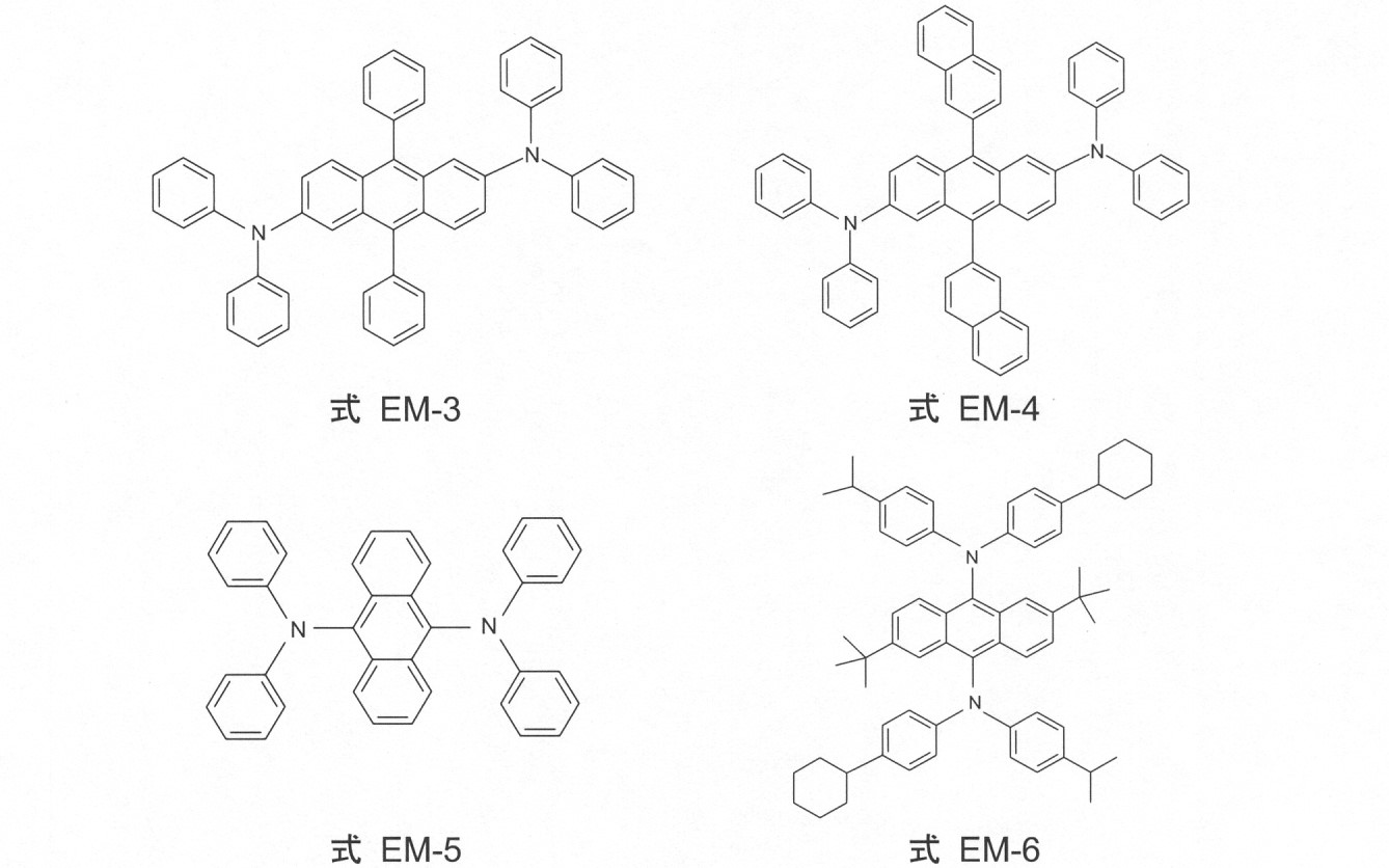
特に好ましいスチリルアミン化合物は、US7250532B2に記載の式EM-1の化合物、およびDE102005058557A1に記載の式EM-2の化合物である: Particularly preferred styrylamine compounds are the compound of formula EM-1 described in US7250532B2 and the compound of formula EM-2 described in DE102005058557A1:

特に好ましいトリアリールアミン化合物は、CN1583691A、JP08/053397AおよびUS6251531B1、EP1957606A1、US2008/0113101A1、US2006/210830A、WO2008/006449、ならびにDE102008035413に開示されている式EM-3~EM-15の化合物とその誘導体である: Particularly preferred triarylamine compounds are compounds of formula EM-3 to EM-15 and derivatives thereof disclosed in CN1583691A, JP08/053397A and US6251531B1, EP1957606A1, US2008/0113101A1, US2006/210830A, WO2008/006449 and DE102008035413. is:

蛍光発光体として利用できるさらなる好ましい化合物は、ナフタレン、アントラセン、テトラセン、ベンゾアントラセン、ベンゾフェナントレン(DE102009005746)、フルオレン、フルオランテン、ペリフランテン、インデノペリレン、フェナントレン、ペリレン(US2007/0252517A1)、ピレン、クリセン、デカシクレン、コロネン、テトラフェニルシクロペンタジエン、ペンタフェニルシクロペンタジエン、フルオレン、スピロフルオレン、ルブレン、クマリン(US4769292、US6020078、US2007/0252517A1)、ピラン、オキサゾール、ベンゾオキサゾール、ベンゾチアゾール、ベンゾイミダゾール、ピラジン、ケイ皮酸エステル、ジケトピロロピロール、アクリドン、およびキナクリドン(US2007/0252517A1)の誘導体から選択される。 Further preferred compounds that can be used as fluorescent emitters are naphthalene, anthracene, tetracene, benzanthracene, benzophenanthrene (DE 102009005746), fluorene, fluoranthene, periflanthene, indenoperylene, phenanthrene, perylene (US 2007/0252517 A1), pyrene, chrysene, decacyclene. , coronene, tetraphenylcyclopentadiene, pentaphenylcyclopentadiene, fluorene, spirofluorene, rubrene, coumarin (US4769292, US6020078, US2007/0252517A1), pyran, oxazole, benzoxazole, benzothiazole, benzimidazole, pyrazine, cinnamate , diketopyrrolopyrroles, acridones, and derivatives of quinacridones (US2007/0252517A1).
アントラセン化合物のうち、9,10-置換アントラセン、たとえば9,10-ジフェニルアントラセンおよび9,10-ビス(フェニルエチニル)アントラセンなどが特に好ましい。1,4-ビス(9’-エチニルアントラセニル)-ベンゼンも好ましいドーパントである。 Among anthracene compounds, 9,10-substituted anthracenes, such as 9,10-diphenylanthracene and 9,10-bis(phenylethynyl)anthracene, are particularly preferred. 1,4-bis(9'-ethynylanthracenyl)-benzene is also a preferred dopant.
同様に、ルブレン、クマリン、ローダミン、キナクリドンの誘導体、たとえばDMQA(=N,N’-ジメチルキナクリドン)など、ジシアノメチレンピラン、たとえばDCM(=4-(ジシアノエチレン)-6-(4-ジメチルアミノスチリル-2-メチル)-4H-ピラン)など、チオピラン、ポリメチン、ピリリウムおよびチアピリリウム塩、ペリフランテン、ならびにインデノペリレンが好ましい。 Similarly, derivatives of rubrene, coumarin, rhodamine, quinacridones such as DMQA (=N,N'-dimethylquinacridone), dicyanomethylenepyrans such as DCM (=4-(dicyanoethylene)-6-(4-dimethylaminostyryl) -2-methyl)-4H-pyran), thiopyrans, polymethines, pyrylium and thiapyrylium salts, periflanthenes, and indenoperylenes are preferred.
青色蛍光発光体は、好ましくはポリ芳香族化合物、たとえば9,10-ジ(2-ナフチルアントラセン)および他のアントラセン誘導体など、テトラセン、キサンテン、ペリレンの誘導体、たとえば2,5,8,11-テトラ-t-ブチルペリレンなど、フェニレン、たとえば4,4’-ビス(9-エチル-3-カルバゾビニレン)-1,1’-ビフェニル、フルオレン、フルオランテン、アリールピレン(US2006/0222886A1)、アリーレンビニレン(US5121029、US5130603)、ビス(アジニル)イミン-ホウ素化合物(US2007/0092753A1)、ビス(アジニル)メテン化合物、およびカルボスチリル化合物などである。 Blue fluorescent emitters are preferably polyaromatic compounds such as 9,10-di(2-naphthylanthracene) and other anthracene derivatives, derivatives of tetracene, xanthene, perylene such as 2,5,8,11-tetra -t-butylperylene and the like, phenylenes such as 4,4'-bis(9-ethyl-3-carbazovinylene)-1,1'-biphenyl, fluorene, fluoranthene, arylpyrene (US2006/0222886A1), arylenevinylene (US5121029, US5130603), bis(azinyl)imine-boron compounds (US2007/0092753A1), bis(azinyl)methene compounds, and carbostyryl compounds.
さらなる好ましい青色蛍光発光体は、C.H.Chenら:「Recent developments in organic electroluminescent materials」Macro-mol.Symp.125、(1997)1-48および「Recent progress of molecular organic electroluminescent materials and devices」Mat.Sci.and Eng.R、39(2002)、143-222に記載されている。 Further preferred blue fluorescent emitters are C.I. H. Chen et al.: "Recent developments in organic electroluminescent materials" Macro-mol. Symp. 125, (1997) 1-48 and "Recent progress of molecular organic electroluminescent materials and devices" Mat. Sci. and Eng. R, 39 (2002), 143-222.
さらなる好ましい青色蛍光発光体は、DE102008035413に開示されている炭化水素である。 Further preferred blue fluorescent emitters are the hydrocarbons disclosed in DE102008035413.
リン光発光体として機能することができる好ましい化合物を、以下の例により記載する。 Preferred compounds that can function as phosphorescent emitters are described by the following examples.
リン光発光体の例が、WO00/70655、WO01/41512、WO02/02714、WO02/15645、EP1191613、EP1191612、EP1191614、およびWO2005/033244によって明らかにされている。一般に、先行技術に従いリン光OLEDに使用され、有機エレクトロルミネッセンスの分野で当業者に公知であるようなリン光錯体は全て適切であり、当業者は、進歩性を要することなくさらなるリン光錯体を使用することができる。 Examples of phosphorescent emitters are disclosed by WO00/70655, WO01/41512, WO02/02714, WO02/15645, EP1191613, EP1191612, EP1191614 and WO2005/033244. In general, all phosphorescent complexes such as those used in phosphorescent OLEDs according to the prior art and known to the person skilled in the art in the field of organic electroluminescence are suitable, and the person skilled in the art will be able to formulate further phosphorescent complexes without inventive step. can be used.
リン光金属錯体は、好ましくはIr、Ru、Pd、Pt、OsまたはReを含有する。 The phosphorescent metal complex preferably contains Ir, Ru, Pd, Pt, Os or Re.
好ましい配位子は、2-フェニルピリジン誘導体、7,8-ベンゾキノリン誘導体、2-(2-チエニル)ピリジン誘導体、2-(1-ナフチル)ピリジン誘導体、1-フェニルイソキノリン誘導体、3-フェニルイソキノリン誘導体、または2-フェニルキノリン誘導体である。これらの化合物は全て、青色用に、たとえばフルオロ、シアノおよび/またはトリフルオロメチル置換基により置換されていてもよい。補助配位子は、好ましくはアセチルアセトナートまたはピコリン酸である。 Preferred ligands are 2-phenylpyridine derivatives, 7,8-benzoquinoline derivatives, 2-(2-thienyl)pyridine derivatives, 2-(1-naphthyl)pyridine derivatives, 1-phenylisoquinoline derivatives, 3-phenylisoquinoline derivatives, or 2-phenylquinoline derivatives. All these compounds may be substituted for the blue color, eg by fluoro, cyano and/or trifluoromethyl substituents. The ancillary ligand is preferably acetylacetonate or picolinic acid.
好ましくは、有機半導体化合物の少なくとも1種は、光を発し、加えて原子番号が38より大きい少なくとも1種の原子を含有する有機リン光化合物である。 Preferably, at least one of the organic semiconductor compounds is an organic phosphorescent compound that emits light and additionally contains at least one atom with an atomic number greater than 38.
好ましくは、リン光化合物は、式(EM-16)~(EM-19): Preferably, the phosphorescent compound has formulas (EM-16) to (EM-19):

(式中、
DCyは、出現する毎に同一であるかまたは異なり、少なくとも1個の供与体原子、好ましくは窒素、カルベンの形態の炭素、またはリンを含有する環状基であり、この環状基はこの供与体原子を介して金属に結合し、また、1つ以上の置換基Raを有していてもよく;基DCyとCCyは、共有結合を介して互いに結合しており;
CCyは、出現する毎に同一であるかまたは異なり、炭素原子を含有する環状基であり、この環状基はこの炭素原子を介して金属に結合しており、また、1つ以上の置換基Raを有していてもよく;
Aは、出現する毎に同一であるかまたは異なり、モノアニオン性二座キレート配位子、好ましくはジケトナート配位子であり;
Raは、それぞれの場合において同一であるかまたは異なり、F、Cl、Br、I、NO2、CN、1~20個の炭素原子を有する直鎖、分枝もしくは環状アルキルもしくはアルコキシ基(ここで、1つ以上の隣接していないCH2基は、-O-、-S-、-NRb-、-CONRb-、-CO-O-、-C=O-、-CH=CH-または-C≡C-によって置きかえられていてもよく、1個以上の水素原子は、Fによって置きかえられていてもよい)、または4~14個の炭素原子を有し、1つ以上のRcラジカルによって置換されていてもよいアリールもしくはヘテロアリール基であり、複数の置換基Raはまた、同じ環上または2つの異なる環上のいずれかで、一緒になって単環もしくは多環式の脂肪族もしくは芳香族環系を形成してもよく;
Rbは、それぞれの場合において同一であるかまたは異なり、1~20個の炭素原子を有する直鎖、分枝もしくは環状アルキルもしくはアルコキシ基(ここで、1つ以上の隣接していないCH2基は、-O-、-S-、-CO-O-、-C=O-、-CH=CH-または-C≡C-によって置きかえられていてもよく、1個以上の水素原子は、Fによって置きかえられていてもよい)、または4~14個の炭素原子を有し、1つ以上のRcラジカルによって置換されていてもよいアリールもしくはヘテロアリール基であり;
Rcは、それぞれの場合において同一であるかまたは異なり、1~20個の炭素原子を有する直鎖、分枝もしくは環状アルキルもしくはアルコキシ基(ここで、1つ以上の隣接していないCH2基は、-O-、-S-、-CO-O-、-C=O-、-CH=CH-または-C≡C-、によって置きかえられていてもよく、1個以上の水素原子は、Fによって置きかえられていてもよい)である)
の化合物である。
(In the formula,
DCy is a cyclic group, identical or different at each occurrence, containing at least one donor atom, preferably nitrogen, carbon in the form of a carbene, or phosphorus, which cyclic group is the donor atom and may also carry one or more substituents R a ; the groups DCy and CCy are linked to each other via a covalent bond;
CCy, which may be the same or different at each occurrence, is a cyclic group containing a carbon atom, which is attached to the metal through this carbon atom, and one or more substituents R a ;
A is, identical or different at each occurrence, a monoanionic bidentate chelating ligand, preferably a diketonate ligand;
R a is in each case the same or different and is F, Cl, Br, I, NO 2 , CN, a linear, branched or cyclic alkyl or alkoxy group having 1 to 20 carbon atoms (here and one or more non-adjacent CH 2 groups are -O-, -S-, -NR b -, -CONR b -, -CO-O-, -C=O-, -CH=CH- or -C≡C-, and one or more hydrogen atoms may be replaced by F), or having 4 to 14 carbon atoms and one or more R c an aryl or heteroaryl group optionally substituted by radicals, wherein multiple substituents R a also together, either on the same ring or on two different rings, are monocyclic or polycyclic may form an aliphatic or aromatic ring system;
R b is the same or different in each case and is a linear, branched or cyclic alkyl or alkoxy group having 1 to 20 carbon atoms (wherein one or more non-adjacent CH 2 groups may be replaced by -O-, -S-, -CO-O-, -C=O-, -CH=CH- or -C≡C- and one or more hydrogen atoms may be replaced by F or an aryl or heteroaryl group having 4 to 14 carbon atoms, optionally substituted by one or more R c radicals;
R c is the same or different in each case and is a linear, branched or cyclic alkyl or alkoxy group having 1 to 20 carbon atoms (wherein one or more non-adjacent CH 2 groups is optionally replaced by -O-, -S-, -CO-O-, -C=O-, -CH=CH- or -C≡C-, and one or more hydrogen atoms are may be replaced by F)
is a compound of
上述のような基は、当技術分野で公知である。追加の情報は、上記および下記のような明確な例によって提供される。さらに、基CCy、DCy、A、Ra、RbおよびRcの具体例は、たとえば文献WO2015018480A1において提供されており、この文献は、リン光化合物に関するその開示について、参照することによりここに明示的に組み込まれる。 Groups such as those described above are known in the art. Additional information is provided by specific examples such as those above and below. Further examples of the groups CCy, DCy , A , Ra, Rb and Rc are provided for example in the document WO2015018480A1, which is hereby incorporated by reference for its disclosure on phosphorescent compounds. incorporated into the system.
特に、式EM-20の四座配位子を有するPtまたはPdの錯体が適している。 Particularly suitable are complexes of Pt or Pd with tetradentate ligands of formula EM-20.

式EM-20の化合物は、US2007/0087219A1により詳細に記載されており、ここで、上記式中の置換基と添え字の説明のため、開示を目的としてこの明細書を参照する。さらに、拡張環系を有するPt-ポルフィリン錯体(US2009/0061681A1)およびIr錯体、たとえば2,3,7,8,12,13,17,18-オクタエチル-21H、23H-ポルフィリン-Pt(II)、テトラフェニル-Pt(II)テトラベンゾポルフィリン(US2009/0061681A1)、cis-ビス(2-フェニルピリジナト-N,C2’)Pt(II)、cis-ビス(2-(2’-チエニル)ピリジナト-N,C3’)Pt(II)、cis-ビス(2-(2’-チエニル)-キノリナト-N,C5’)Pt(II)、(2-(4,6-ジフルオロフェニル)ピリジナト-N,C2’)Pt(II)(アセチルアセトナート)、またはトリス(2-フェニルピリジナト-N,C2’)Ir(III)(=Ir(ppy)3、緑色)、ビス(2-フェニルピリジナト-N,C2)Ir(III)(アセチルアセトナート)(=Ir(ppy)2アセチルアセトナート、緑色、US2001/0053462A1、Baldo、Thompsonら、Nature 403、(2000)、750-753)、ビス(1-フェニルイソキノリナト-N,C2’)(2-フェニルピリジナト-N,C2’)イリジウム(III)、ビス(2-フェニルピリジナト-N,C2’)(1-フェニルイソキノリナト-N,C2’)イリジウム(III)、ビス(2-(2’-ベンゾチエニル)ピリジナト-N,C3’)イリジウム(III)(アセチルアセトナート)、ビス(2-(4’,6’-ジフルオロフェニル)ピリジナト-N,C2’)イリジウム(III)(ピコリナート)(FIrpic、青色)、ビス(2-(4’,6’-ジフルオロフェニル)ピリジナト-N,C2’)Ir(III)(テトラキス(1-ピラゾリル)ボラート)、トリス(2-(ビフェニル-3-イル)-4-tert-ブチルピリジン)イリジウム(III)、(ppz)2Ir(5phdpym)(US2009/0061681A1)、(45ooppz)2Ir(5phdpym)(US2009/0061681A1)、2-フェニルピリジン-Ir錯体の誘導体、たとえばPQIr(=イリジウム(III)ビス(2-フェニルキノリル-N,C2’)アセチルアセトナート)など、トリス(2-フェニルイソキノリナト-N,C)Ir(III)(赤色)、ビス(2-(2’-ベンゾ[4,5-a]チエニル)ピリジナト-N,C3)Ir(アセチルアセトナート)([Btp2Ir(acac)]、赤色、Adachiら、Appl.Phys.Lett.78(2001)、1622-1624)である。 The compound of formula EM-20 is described in more detail in US 2007/0087219 A1, to which reference is made herein for purposes of disclosure for the explanation of the substituents and subscripts in the above formula. Additionally, Pt-porphyrin complexes with extended ring systems (US2009/0061681A1) and Ir complexes such as 2,3,7,8,12,13,17,18-octaethyl-21H, 23H-porphyrin-Pt(II), Tetraphenyl-Pt(II) tetrabenzoporphyrin (US2009/0061681A1), cis-bis(2-phenylpyridinato-N,C 2 ')Pt(II), cis-bis(2-(2'-thienyl) pyridinato-N,C 3 ′)Pt(II), cis-bis(2-(2′-thienyl)-quinolinato-N,C 5 ′)Pt(II), (2-(4,6-difluorophenyl) pyridinato-N,C 2 ′)Pt(II) (acetylacetonate) or tris(2-phenylpyridinato-N,C 2 ′)Ir(III) (=Ir(ppy) 3 , green), bis (2-phenylpyridinato-N,C 2 )Ir(III) (acetylacetonate) (=Ir(ppy) 2 acetylacetonate, green, US2001/0053462A1, Baldo, Thompson et al., Nature 403, (2000) , 750-753), bis(1-phenylisoquinolinato-N,C 2 ′)(2-phenylpyridinato-N,C 2 ′)iridium(III), bis(2-phenylpyridinato-N ,C 2 ′)(1-phenylisoquinolinato-N,C 2 ′)iridium(III), bis(2-(2′-benzothienyl)pyridinato-N,C 3 ′)iridium(III) (acetylaceto nate), bis(2-(4′,6′-difluorophenyl)pyridinato-N,C 2 ′)iridium(III) (picolinate) (FIrpic, blue), bis(2-(4′,6′-difluoro Phenyl)pyridinato-N,C 2 ′)Ir(III) (tetrakis(1-pyrazolyl)borate), tris(2-(biphenyl-3-yl)-4-tert-butylpyridine)iridium(III), (ppz ) 2 Ir(5phdpym) (US2009/0061681A1), (45ooppz) 2Ir(5phdpym) (US2009/0061681A1), derivatives of 2 -phenylpyridine-Ir complexes such as PQIr (=iridium(III) bis(2-phenylquino lyl-N,C 2 ')acetylacetonate), tris(2-phenylisocyanate) Norinato-N,C)Ir(III) (red), bis(2-(2′-benzo[4,5-a]thienyl)pyridinato-N,C 3 )Ir (acetylacetonate) ([Btp 2 Ir (acac)], red, Adachi et al., Appl. Phys. Lett. 78 (2001), 1622-1624).
同様に適するのは、三価のランタニド、たとえばTb3+およびEu3+などの錯体(J.Kidoら、Appl.Phys.Lett.65(1994)、2124、Kidoら、Chem.Lett.657、1990、US2007/0252517A1)、またはマレオニトリルジチオレートを含むPt(II)、Ir(I)、Rh(I)のリン光錯体(Johnsonら、JACS105、1983、1795)、Re(I)トリカルボニル-ジイミン錯体(とりわけWrighton、JACS96、1974、998)、シアノ配位子とビピリジルまたはフェナントロリン配位子を有するOs(II)錯体(Maら、Synth.Metals94、1998、245)である。 Also suitable are complexes of trivalent lanthanides, such as Tb 3+ and Eu 3+ (J. Kido et al., Appl. Phys. Lett. 65 (1994), 2124; Kido et al., Chem. Lett. 657, 1990; US 2007/0252517 A1), or phosphorescent complexes of Pt(II), Ir(I), Rh(I) with maleonitrile dithiolate (Johnson et al., JACS 105, 1983, 1795), Re(I) tricarbonyl-diimine complexes (Inter alia Wrighton, JACS 96, 1974, 998), Os(II) complexes with cyano ligands and bipyridyl or phenanthroline ligands (Ma et al., Synth. Metals 94, 1998, 245).
三座配位子を有するさらなるリン光発光体が、US6824895およびUS10/729238に記載されている。赤色発光リン光錯体は、US6835469およびUS6830828に見出される。 Further phosphorescent emitters with tridentate ligands are described in US6824895 and US10/729238. Red-emitting phosphorescent complexes are found in US6835469 and US6830828.
リン光ドーパントとして使用される特に好ましい化合物は、とりわけUS2001/0053462A1およびInorg.Chem.2001、40(7)、1704-1711、JACS2001、123(18)、4304-4312に記載の式EM-21の化合物とその誘導体である。 Particularly preferred compounds for use as phosphorescent dopants are described inter alia in US 2001/0053462 A1 and Inorg. Chem. 2001, 40(7), 1704-1711, JACS 2001, 123(18), 4304-4312 and compounds of formula EM-21 and derivatives thereof.

誘導体は、US7378162B2、US6835469B2およびJP2003/253145Aに記載されている。 Derivatives are described in US7378162B2, US6835469B2 and JP2003/253145A.
さらに、US7238437B2、US2009/008607A1およびEP1348711に記載の式EM-22~EM-25の化合物とその誘導体を、発光体として利用できる。 Additionally, compounds of formulas EM-22 to EM-25 and their derivatives as described in US7238437B2, US2009/008607A1 and EP1348711 can be utilized as emitters.

同様に、量子ドットを発光体として利用することができ、これらの材料は、WO2011/076314A1に詳細に開示されている。 Quantum dots can likewise be used as emitters and these materials are disclosed in detail in WO2011/076314A1.
特に、発光化合物と共にホスト材料として利用される化合物は、物質の様々なクラスからの材料を含む。 In particular, compounds utilized as host materials in conjunction with emissive compounds include materials from various classes of substances.
ホスト材料は一般に、利用される発光体材料よりもHOMOとLUMOの間に大きいバンドギャップを有する。加えて、好ましいホスト材料は、正孔または電子輸送材料いずれかの特性を示す。さらに、ホスト材料は、電子および正孔輸送特性の両方を有することができる。 The host material generally has a larger bandgap between HOMO and LUMO than the emitter material utilized. In addition, preferred host materials exhibit the properties of either hole or electron transport materials. Additionally, the host material can have both electron and hole transport properties.
ホスト材料は、場合により、特にホスト材料がOLEDにおいてリン光発光体と組み合わせて利用される場合、マトリックス材料とも呼ばれる。 A host material is sometimes also called a matrix material, especially when the host material is used in combination with a phosphorescent emitter in an OLED.
特に蛍光ドーパントと共に利用される好ましいホスト材料またはコホスト材料は、オリゴアリーレン(たとえば、EP676461による2,2’,7,7’-テトラフェニルスピロビフルオレン、またはジナフチルアントラセン)、特に縮合芳香族基を含有するオリゴアリーレン、たとえばアントラセン、ベンゾアントラセン、ベンゾフェナントレン(DE102009005746、WO2009/069566)、フェナントレン、テトラセン、コロネン、クリセン、フルオレン、スピロフルオレン、ペリレン、フタロペリレン、ナフタロペリレン、デカシクレン、ルブレンなど、オリゴアリーレンビニレン(たとえばEP676461によるDPVBi=4,4’-ビス(2,2-ジフェニルエテニル)-1,1’-ビフェニルもしくはスピロ-DPVBi)、ポリポダル金属錯体(たとえばWO04/081017による)、特に8-ヒドロキシキノリンの金属錯体、たとえばAlQ3(=アルミニウム(III)トリス(8-ヒドロキシキノリン))もしくはビス(2-メチル-8-キノリノラト)-4-(フェニルフェノリノラト)アルミニウムの金属錯体であって、さらにイミダゾールキレートを含むもの(US2007/0092753A1)、およびキノリン金属錯体、アミノキノリン-金属錯体、ベンゾキノリン-金属錯体、正孔伝導化合物(たとえばWO2004/058911による)、電子伝導化合物、特にケトン、ホスフィンオキシド、スルホキシドなど(たとえばWO2005/084081およびWO2005/084082による)、アトロプ異性体(たとえばWO2006/048268による)、ボロン酸誘導体(たとえばWO2006/117052による)またはベンゾアントラセン(たとえばWO2008/145239による)のクラスから選択される。 Preferred host or co-host materials, especially for use with fluorescent dopants, are oligoarylenes (e.g. 2,2',7,7'-tetraphenylspirobifluorene or dinaphthylanthracene according to EP 676461), especially fused aromatic groups. containing oligoarylenes such as anthracene, benzoanthracene, benzophenanthrene (DE102009005746, WO2009/069566), phenanthrene, tetracene, coronene, chrysene, fluorene, spirofluorene, perylene, phthaloperylene, naphthaloperylene, decacyclene, rubrene, etc., oligoarylenevinylenes (for example DPVBi according to EP 676461 = 4,4′-bis(2,2-diphenylethenyl)-1,1′-biphenyl or spiro-DPVBi), polypodal metal complexes (for example according to WO 04/081017), especially metals of 8-hydroxyquinoline complexes, for example metal complexes of AlQ 3 (=aluminium(III) tris(8-hydroxyquinoline)) or bis(2-methyl-8-quinolinolato)-4-(phenylphenolato)aluminum, additionally imidazole chelates (US 2007/0092753 A1), and quinoline metal complexes, aminoquinoline-metal complexes, benzoquinoline-metal complexes, hole-conducting compounds (for example according to WO2004/058911), electron-conducting compounds, especially ketones, phosphine oxides, sulfoxides, etc. (eg according to WO2005/084081 and WO2005/084082), atropisomers (eg according to WO2006/048268), boronic acid derivatives (eg according to WO2006/117052) or benzanthracenes (eg according to WO2008/145239).
ホスト材料またはコホスト材料として機能できる特に好ましい化合物は、アントラセン、ベンゾアントラセンおよび/もしくはピレンを含むオリゴアリーレン、またはこれらの化合物のアトロプ異性体のクラスから選択される。本発明の意味でのオリゴアリーレンは、少なくとも3つのアリールまたはアリーレン基が互いに結合している化合物を意味するものと理解されることが意図される。 Particularly preferred compounds capable of functioning as host or co-host materials are selected from the class of oligoarylenes, including anthracene, benzanthracene and/or pyrene, or atropisomers of these compounds. An oligoarylene in the sense of the invention is intended to be understood as meaning a compound in which at least three aryl or arylene groups are attached to one another.
好ましいホスト材料は、特に式(H-1)の化合物から選択され、 Preferred host materials are selected especially from compounds of formula (H-1),
![]()
![]()
(式中、Ar4、Ar5、Ar6は、出現する毎に同一であるかまたは異なり、任意に置換されていてもよい5~30個の芳香族環原子を有するアリールまたはヘテロアリール基であり、pは、1~5の範囲の整数を表し;Ar4、Ar5およびAr6の中のπ電子の合計は、p=1ならば少なくとも30、p=2ならば少なくとも36、p=3ならば少なくとも42である)。 (wherein Ar 4 , Ar 5 and Ar 6 are the same or different at each occurrence and are optionally substituted aryl or heteroaryl groups having 5 to 30 aromatic ring atoms; and p represents an integer ranging from 1 to 5; the sum of π electrons in Ar 4 , Ar 5 and Ar 6 is at least 30 if p=1, at least 36 if p=2, p= 3 is at least 42).
式(H-1)の化合物において、Ar5基は、特に好ましくはアントラセンを表し、Ar4およびAr6基は、9および10位で結合しており、ここで、これらの基は、任意に置換されていてもよい。特に非常に好ましくは、Ar4および/またはAr6基の少なくとも一方が、1-もしくは2-ナフチル、2-、3-もしくは9-フェナントレニル、または2-、3-、4-、5-、6-もしくは7-ベンゾアントラセニルから選択される縮合アリール基である。アントラセン系化合物は、US2007/0092753A1およびUS2007/0252517A1に記載されており、たとえば2-(4-メチルフェニル)-9,10-ジ-(2-ナフチル)アントラセン、9-(2-ナフチル)-10-(1,1’-ビフェニル)アントラセンおよび9,10-ビス[4-(2,2-ジフェニルエテニル)フェニル]アントラセン、9,10-ジフェニルアントラセン、9,10-ビス(フェニルエチニル)アントラセン、ならびに1,4-ビス(9’-エチニルアントラセニル)ベンゼンである。2つのアントラセン単位を含有する化合物(US2008/0193796A1)、たとえば10,10’-ビス[1,1’,4’,1’’]テルフェニル-2-イル-9,9’-ビスアントラセニルも好ましい。 In compounds of formula (H-1), the Ar 5 group particularly preferably represents anthracene, the Ar 4 and Ar 6 groups are bonded at the 9 and 10 positions, wherein these groups optionally may be substituted. Very particularly preferably at least one of the Ar 4 and/or Ar 6 groups is 1- or 2-naphthyl, 2-, 3- or 9-phenanthrenyl or 2-, 3-, 4-, 5-, 6- is a condensed aryl group selected from - or 7-benzoanthracenyl. Anthracene-based compounds are described in US2007/0092753A1 and US2007/0252517A1, for example 2-(4-methylphenyl)-9,10-di-(2-naphthyl)anthracene, 9-(2-naphthyl)-10 -(1,1′-biphenyl)anthracene and 9,10-bis[4-(2,2-diphenylethenyl)phenyl]anthracene, 9,10-diphenylanthracene, 9,10-bis(phenylethynyl)anthracene, and 1,4-bis(9′-ethynylanthracenyl)benzene. Compounds containing two anthracene units (US2008/0193796A1) such as 10,10'-bis[1,1',4',1'']terphenyl-2-yl-9,9'-bisanthracenyl is also preferred.
さらなる好ましい化合物は、アリールアミン、スチリルアミン、フルオレセイン、ジフェニルブタジエン、テトラフェニルブタジエン、シクロペンタジエン、テトラフェニルシクロペンタジエン、ペンタフェニルシクロペンタジエン、クマリン、オキサジアゾール、ビスベンゾオキサゾリン、オキサゾール、ピリジン、ピラジン、イミン、ベンゾチアゾール、ベンゾオキサゾール、ベンゾイミダゾール(US2007/0092753A1)の誘導体、たとえば2,2’,2’’-(1,3,5-フェニレン)トリス[1-フェニル-1H-ベンゾイミダゾール]、アルダジン、スチルベン、スチリルアリーレン誘導体、たとえば9,10-ビス[4-(2,2-ジフェニルエテニル)-フェニル]アントラセン、およびジスチリルアリーレン誘導体(US5121029)、ジフェニルエチレン、ビニルアントラセン、ジアミノカルバゾール、ピラン、チオピラン、ジケトピロロピロール、ポリメチン、ケイ皮酸エステル、ならびに蛍光染料である。 Further preferred compounds are arylamines, styrylamines, fluoresceins, diphenylbutadiene, tetraphenylbutadiene, cyclopentadiene, tetraphenylcyclopentadiene, pentaphenylcyclopentadiene, coumarins, oxadiazoles, bisbenzoxazolines, oxazoles, pyridines, pyrazines, imines , benzothiazole, benzoxazole, derivatives of benzimidazole (US2007/0092753A1) such as 2,2′,2″-(1,3,5-phenylene)tris[1-phenyl-1H-benzimidazole], aldazine, Stilbene, styrylarylene derivatives such as 9,10-bis[4-(2,2-diphenylethenyl)-phenyl]anthracene and distyrylarylene derivatives (US5121029), diphenylethylene, vinylanthracene, diaminocarbazole, pyran, thiopyran , diketopyrrolopyrroles, polymethines, cinnamates, and fluorescent dyes.
アリールアミンおよびスチリルアミンの誘導体、たとえばTNB(=4,4’-ビス[N-(1-ナフチル)-N-(2-ナフチル)アミノ]ビフェニル)が特に好ましい。金属オキシノイド錯体、たとえばLiQまたはAlQ3をコホストとして使用することができる。 Derivatives of arylamines and styrylamines such as TNB (=4,4′-bis[N-(1-naphthyl)-N-(2-naphthyl)amino]biphenyl) are particularly preferred. Metal oxinoid complexes such as LiQ or AlQ3 can be used as cohosts.
オリゴアリーレンをマトリックスとして含む好ましい化合物が、US2003/0027016A1、US7326371B2、US2006/043858A、WO2007/114358、WO2008/145239、JP3148176B2、EP1009044、US2004/018383、WO2005/061656A1、EP0681019B1、WO2004/013073A1、US5077142、WO2007/065678、およびDE102009005746に開示されており、ここで、特に好ましい化合物を式H-2~H-8により記載する。 オリゴアリーレンをマトリックスとして含む好ましい化合物が、US2003/0027016A1、US7326371B2、US2006/043858A、WO2007/114358、WO2008/145239、JP3148176B2、EP1009044、US2004/018383、WO2005/061656A1、EP0681019B1、WO2004/013073A1、US5077142、WO2007/ 065678, and DE 102009005746, where particularly preferred compounds are described by formulas H-2 to H-8.

さらに、ホストまたはマトリックスとして利用できる化合物として、リン光発光体と共に利用される材料が挙げられる。 Additionally, compounds that can be used as hosts or matrices include materials that are used with phosphorescent emitters.
これらの化合物は、ポリマー中の構造要素として利用することもでき、CBP(N,N-ビスカルバゾリルビフェニル)、カルバゾール誘導体(たとえばWO2005/039246、US2005/0069729、JP2004/288381、EP1205527またはWO2008/086851による)、アザカルバゾール(たとえばEP1617710、EP1617711、EP1731584またはJP2005/347160による)、ケトン(たとえばWO2004/093207またはDE102008033943による)、ホスフィンオキシド、スルホキシドおよびスルホン(たとえばWO2005/003253による)、オリゴフェニレン、芳香族アミン(たとえばUS2005/0069729による)、双極性マトリックス材料(たとえばWO2007/137725による)、シラン(たとえばWO2005/111172による)、9,9-ジアリールフルオレン誘導体(たとえばDE102008017591による)、アザボロールまたはボロン酸エステル(たとえばWO2006/117052による)、トリアジン誘導体(たとえばDE102008036982による)、インドロカルバゾール誘導体(たとえばWO2007/063754またはWO2008/056746による)、インデノカルバゾール誘導体(たとえばDE102009023155およびDE102009031021による)、ジアザホスホール誘導体(たとえばDE102009022858による)、トリアゾール誘導体、オキサゾールおよびオキサゾール誘導体、イミダゾール誘導体、ポリアリールアルカン誘導体、ピラゾリン誘導体、ピラゾロン誘導体、ジスチリルピラジン誘導体、チオピランジオキシド誘導体、フェニレンジアミン誘導体、第3級芳香族アミン、スチリルアミン、アミノ置換カルコン誘導体、インドール、ヒドラゾン誘導体、スチルベン誘導体、シラザン誘導体、芳香族ジメチリデン化合物、カルボジイミド誘導体、トリアリールアミノフェノール配位子をさらに含有してもよい8-ヒドロキシキノリン誘導体の金属錯体、たとえばAlQ3(US2007/0134514A1)、金属錯体/ポリシラン化合物、ならびにチオフェン、ベンゾチオフェンおよびジベンゾチオフェン誘導体が挙げられる。 These compounds can also be utilized as structural elements in polymers, CBP (N,N-biscarbazolylbiphenyl), carbazole derivatives (eg WO2005/039246, US2005/0069729, JP2004/288381, EP1205527 or 086851), azacarbazoles (for example according to EP 1617710, EP 1617711, EP 1731584 or JP 2005/347160), ketones (for example according to WO 2004/093207 or DE 102008033943), phosphine oxides, sulfoxides and sulfones (for example according to WO 2005/003253, aromatics), oligophenylenes amines (for example according to US 2005/0069729), bipolar matrix materials (for example according to WO 2007/137725), silanes (for example according to WO 2005/111172), 9,9-diarylfluorene derivatives (for example according to DE 102008017591), azaborol or boronic esters (for example WO 2006/117052), triazine derivatives (e.g. according to DE 102008036982), indolocarbazole derivatives (e.g. according to WO 2007/063754 or WO 2008/056746), indenocarbazole derivatives (e.g. according to DE 102009023155 and DE 102009031021), diazaphosphole derivatives (e.g. 050D8021) triazole derivatives, oxazoles and oxazole derivatives, imidazole derivatives, polyarylalkane derivatives, pyrazoline derivatives, pyrazolone derivatives, distyrylpyrazine derivatives, thiopyran dioxide derivatives, phenylenediamine derivatives, tertiary aromatic amines, styrylamines, amino-substituted chalcone derivatives, indoles, hydrazone derivatives, stilbene derivatives, silazane derivatives, aromatic dimethylidene compounds, carbodiimide derivatives, metal complexes of 8-hydroxyquinoline derivatives which may further contain triarylaminophenol ligands, such as AlQ 3 (US2007/ 0134514 A1), metal complexes/polysilane compounds, and thiophene, benzothiophene and dibenzothiophene derivatives.
好ましいカルバゾール誘導体の例は、mCP(=1,3-N,N-ジ-カルバゾリルベンゼン(=9,9’-(1,3-フェニレン)ビス-9H-カルバゾール))(式H-9)、CDBP(=9,9’-(2,2’-ジメチル[1,1’-ビフェニル]-4,4’-ジイル)ビス-9H-カルバゾール)、1,3-ビス(N,N’-ジカルバゾリル)ベンゼン(=1,3-ビス(カルバゾール-9-イル)ベンゼン)、PVK(ポリビニルカルバゾール)、3,5-ジ(9H-カルバゾール-9-イル)ビフェニル、およびCMTTP(式H-10)である。特に言及される化合物は、US2007/0128467A1およびUS2005/0249976A1に開示されている(式H-11およびH-13)。 An example of a preferred carbazole derivative is mCP (=1,3-N,N-di-carbazolylbenzene (=9,9′-(1,3-phenylene)bis-9H-carbazole)) (formula H-9 ), CDBP (=9,9′-(2,2′-dimethyl[1,1′-biphenyl]-4,4′-diyl)bis-9H-carbazole), 1,3-bis(N,N′ -dicarbazolyl)benzene (=1,3-bis(carbazol-9-yl)benzene), PVK (polyvinylcarbazole), 3,5-di(9H-carbazol-9-yl)biphenyl, and CMTTP (formula H-10) ). Compounds of particular mention are disclosed in US2007/0128467A1 and US2005/0249976A1 (formulas H-11 and H-13).

好ましいテトラアリール-Si化合物が、たとえばUS2004/0209115、US2004/0209116、US2007/0087219A1、およびH.Gilman、E.A.Zuech、Chemistry & Industry(London、United Kingdom)、1960、120に開示されている。 Preferred tetraaryl-Si compounds are described, for example, in US2004/0209115, US2004/0209116, US2007/0087219A1, and H.I. Gilman, E. A. Zuech, Chemistry & Industry (London, United Kingdom), 1960, 120.
特に好ましいテトラアリール-Si化合物を、式H-14~H-20により記載する。 Particularly preferred tetraaryl-Si compounds are described by formulas H-14 to H-20.

リン光ドーパント用のマトリックスの調製に特に好ましい群4からの化合物が、とりわけDE102009022858、DE102009023155、EP652273B1、WO2007/063754およびWO2008/056746に開示されており、ここで、特に好ましい化合物を式H-22~H-25により記載する。 Particularly preferred compounds from group 4 for the preparation of matrices for phosphorescent dopants are disclosed inter alia in DE102009022858, DE102009023155, EP652273B1, WO2007/063754 and WO2008/056746, wherein particularly preferred compounds are of formulas H-22 to Described by H-25.

本発明に従い利用でき、ホスト材料として機能できる機能性化合物に関し、少なくとも1個の窒素原子を含有する物質が特に好ましい。これらは、好ましくは芳香族アミン、トリアジン誘導体およびカルバゾール誘導体を含む。したがって、カルバゾール誘導体は、特に、驚くべき高効率を示す。トリアジン誘導体は、電子デバイスの予期しないほどの長寿命をもたらす。 With respect to functional compounds that can be utilized according to the present invention and that can serve as host materials, materials containing at least one nitrogen atom are particularly preferred. These preferably include aromatic amines, triazine derivatives and carbazole derivatives. Therefore, carbazole derivatives in particular show surprisingly high efficiency. Triazine derivatives provide unexpectedly long lifetimes for electronic devices.
複数の異なるマトリックス材料、特に少なくとも1種の電子伝導マトリックス材料と少なくとも1種の正孔伝導マトリックス材料を混合物として利用することも好ましい場合がある。たとえばWO2010/108579に記載されているような、電荷輸送マトリックス材料と、電荷輸送には関与するとしても顕著な程度には関与しない電気的に不活性なマトリックス材料との混合物の使用も同様に好ましい。 It may also be preferred to utilize a plurality of different matrix materials, in particular at least one electron-conducting matrix material and at least one hole-conducting matrix material, as a mixture. Equally preferred is the use of mixtures of charge transporting matrix materials and electrically inert matrix materials which, if not to a significant extent, participate in charge transport, as described for example in WO 2010/108579. .
一重項状態から三重項状態への移行を改善し、発光体特性を有する機能性化合物の支持に利用され、これらの化合物のリン光特性を改善する化合物を利用することがさらに可能である。この目的に適するのは特に、たとえばWO2004/070772A2およびWO2004/113468A1に記載されているような、カルバゾールおよび架橋カルバゾール二量体単位である。この目的に同じく適切なのは、たとえばWO2005/040302A1に記載されているような、ケトン、ホスフィンオキシド、スルホキシド、スルホン、シラン誘導体および類似の化合物である。 It is further possible to employ compounds that improve the transition from the singlet state to the triplet state, are used to support functional compounds with emissive properties, and improve the phosphorescent properties of these compounds. Suitable for this purpose are in particular carbazole and bridged carbazole dimer units, as described for example in WO2004/070772A2 and WO2004/113468A1. Also suitable for this purpose are ketones, phosphine oxides, sulfoxides, sulfones, silane derivatives and similar compounds, as described, for example, in WO2005/040302A1.
さらに、インクは、ワイドバンドギャップ材料を機能材料として含んでもよい。ワイドバンドギャップ材料は、US7,294,849の開示内容の意味の材料を意味するものと解釈される。これらの系は、エレクトロルミネッセントデバイスにおいて特に有利な性能データを呈する。 Furthermore, the ink may contain a wide bandgap material as a functional material. A wide bandgap material is taken to mean a material within the meaning of the disclosure of US 7,294,849. These systems exhibit particularly advantageous performance data in electroluminescent devices.
ワイドバンドギャップ材料として利用される化合物は、2.5eV以上、より好ましくは3.0eV以上、最も好ましくは3.5eV以上のバンドギャップを好ましくは有することができる。バンドギャップは、とりわけ最高被占分子軌道(HOMO)と最低空分子軌道(LUMO)のエネルギー準位によって計算できる。 Compounds utilized as wide bandgap materials can preferably have a bandgap of 2.5 eV or greater, more preferably 3.0 eV or greater, and most preferably 3.5 eV or greater. The bandgap can be calculated by, among other things, the energy levels of the highest occupied molecular orbital (HOMO) and the lowest unoccupied molecular orbital (LUMO).
さらに、インクは、正孔阻止材料(HBM)を機能材料として含んでもよい。正孔阻止材料は、特にこの材料が発光層または正孔伝導層に隣接する層の形態で配置される場合、多層系において正孔(正電荷)の伝達を防止または最小化する材料を意味する。一般に、正孔阻止材料は、隣接層の中の正孔輸送材料よりも低いHOMO準位を有する。正孔阻止層は多くの場合、OLEDにおいて発光層と電子輸送層の間に配置される。 Additionally, the ink may include a hole blocking material (HBM) as a functional material. By hole-blocking material is meant a material that prevents or minimizes the transport of holes (positive charges) in multilayer systems, especially when this material is arranged in the form of a layer adjacent to the light-emitting layer or the hole-conducting layer. . Generally, hole-blocking materials have a lower HOMO level than hole-transporting materials in adjacent layers. A hole-blocking layer is often placed between the light-emitting layer and the electron-transporting layer in an OLED.
原則として、任意公知の正孔阻止材料を利用することが可能である。本願の他の場所に記載される他の正孔阻止材料に加え、有利な正孔阻止材料は、金属錯体(US2003/0068528)、たとえばビス(2-メチル-8-キノリノラト)(4-フェニルフェノラト)アルミニウム(III)(BAlQ)などである。Fac-トリス(1-フェニルピラゾラト-N,C2)-イリジウム(III)(Ir(ppz)3)がこの目的のために同様に利用されている(US2003/0175553A1)。フェナントロリン誘導体、たとえばBCPなど、またはフタルイミド、たとえばTMPPなども同様に利用できる。 In principle, any known hole blocking material can be used. In addition to other hole-blocking materials described elsewhere in this application, advantageous hole-blocking materials include metal complexes (US2003/0068528) such as bis(2-methyl-8-quinolinolato)(4-phenylpheno Rath)aluminum (III) (BAlQ) and the like. Fac-tris(1-phenylpyrazolato-N,C2)-iridium(III) (Ir(ppz) 3 ) has also been utilized for this purpose (US2003/0175553A1). Phenanthroline derivatives, such as BCP, or phthalimides, such as TMPP, are likewise available.
さらに、有利な正孔阻止材料が、WO00/70655A2、WO01/41512およびWO01/93642A1に記載されている。 Further advantageous hole blocking materials are described in WO00/70655A2, WO01/41512 and WO01/93642A1.
さらに、インクは、電子阻止材料(EBM)を機能材料として含んでもよい。電子阻止材料は、特にこの材料が発光層または電子伝導層に隣接する層の形態で配置される場合、多層系において電子の伝達を防止または最小化する材料を意味する。一般に、電子阻止材料は、隣接層の中の電子輸送材料よりも高いLUMO準位を有する。 Additionally, the ink may include an electron blocking material (EBM) as a functional material. Electron-blocking material means a material that prevents or minimizes the transport of electrons in a multilayer system, especially if this material is arranged in the form of a layer adjacent to the light-emitting layer or the electron-conducting layer. Generally, electron blocking materials have a higher LUMO level than electron transporting materials in adjacent layers.
原則として、任意公知の電子阻止材料を利用することが可能である。本願の他の場所に記載される他の電子阻止材料に加え、有利な電子阻止材料は、遷移金属錯体、たとえばIr(ppz)3(US2003/0175553)などである。 In principle, any known electron blocking material can be used. Advantageous electron blocking materials, in addition to other electron blocking materials described elsewhere in this application, are transition metal complexes such as Ir(ppz) 3 (US 2003/0175553).
電子阻止材料は、好ましくはアミン、トリアリールアミン、およびその誘導体から選択することができる。 Electron blocking materials can preferably be selected from amines, triarylamines and derivatives thereof.
さらに、インクに有機機能材料として利用できる機能性化合物は、低分子量化合物である場合、5,000g/mol以下、好ましくは3,000g/mol以下、より好ましくは2,000g/mol以下、最も好ましくは1,800g/mol以下の分子量を有する。 Furthermore, when the functional compound that can be used as an organic functional material for the ink is a low-molecular-weight compound, it is 5,000 g/mol or less, preferably 3,000 g/mol or less, more preferably 2,000 g/mol or less, most preferably 2,000 g/mol or less. has a molecular weight of 1,800 g/mol or less.
特に興味深いのは、さらに、高いガラス転移温度により特徴付けられる機能性化合物である。これに関連し、インクに有機機能材料として利用できる特に好ましい機能性化合物は、DIN51005(2005-08バージョン)に従い判定されるガラス転移温度が70℃以上、好ましくは100℃以上、より好ましくは125℃以上、最も好ましくは150℃以上のものである。 Also of particular interest are functional compounds characterized by a high glass transition temperature. In this connection, particularly preferred functional compounds that can be used as organic functional materials in inks have a glass transition temperature of 70° C. or higher, preferably 100° C. or higher, more preferably 125° C., determined according to DIN 51005 (2005-08 version). above, most preferably 150° C. or higher.
インクは、ポリマーを有機機能材料としてさらに含んでもよい。有機機能材料として上に記載される化合物は、比較的低分子量を有することが多く、ポリマーと混合することもできる。これらの化合物を共有結合的にポリマーに組み込むことが同様に可能である。これは、特に、反応性脱離基、たとえば臭素、ヨウ素、塩素、ボロン酸もしくはボロン酸エステル、または反応性重合可能基、たとえばオレフィンもしくはオキセタンによって置換された化合物により可能である。これらは、対応するオリゴマー、デンドリマーまたはポリマー製造用のモノマーとして使用することができる。ここでのオリゴマー化または重合は、好ましくは、ハロゲン官能基もしくはボロン酸官能基により、または重合可能基により起きる。さらに、この種の基を介してポリマーを架橋させることが可能である。本発明に有用な化合物とポリマーを、架橋または非架橋層として利用することができる。 The ink may further contain a polymer as an organic functional material. The compounds described above as organic functional materials often have relatively low molecular weights and can also be mixed with polymers. It is likewise possible to incorporate these compounds covalently into polymers. This is possible in particular with compounds substituted by reactive leaving groups such as bromine, iodine, chlorine, boronic acid or boronate esters, or by reactive polymerizable groups such as olefins or oxetanes. They can be used as monomers for the preparation of corresponding oligomers, dendrimers or polymers. Oligomerization or polymerization here preferably takes place via halogen or boronic acid functionalities or via polymerizable groups. Furthermore, it is possible to crosslink the polymer via groups of this type. Compounds and polymers useful in the present invention can be utilized as crosslinked or non-crosslinked layers.
有機機能材料として利用できるポリマーは多くの場合、上記の化合物の文脈において記載した単位または構造要素、とりわけWO02/077060A1、WO2005/014689A2およびWO2011/076314A1において開示され広く記載されたものを含有する。これらは、参照することにより本願に組み込まれる。機能材料は、たとえば下記のクラスに由来するものとすることができる:
群1:正孔注入および/または正孔輸送特性を生成することができる構造要素;
群2:電子注入および/または電子輸送特性を生成することができる構造要素;
群3:群1および群2に関連して記載される特性を併せ持つ構造要素;
群4:発光特性、特にリン光基を有する構造要素;
群5:いわゆる一重項状態から三重項状態への移行を改善する構造要素;
群6:結果として得られるポリマーの形態または発光色に影響を与える構造要素;
群7:典型的には骨格として使用される構造要素。
Polymers that can be used as organic functional materials often contain the units or structural elements described in the context of the above compounds, inter alia those disclosed and extensively described in WO02/077060A1, WO2005/014689A2 and WO2011/076314A1. These are incorporated herein by reference. Functional materials can originate, for example, from the following classes:
Group 1: Structural elements capable of producing hole-injection and/or hole-transport properties;
Group 2: Structural elements capable of producing electron-injection and/or electron-transport properties;
Group 3: Structural elements that combine the properties described in relation to Groups 1 and 2;
Group 4: Structural elements with luminescent properties, in particular phosphorescent groups;
Group 5: Structural elements that improve the transition from the so-called singlet state to the triplet state;
Group 6: Structural elements that influence the morphology or emission color of the resulting polymer;
Group 7: Structural elements typically used as scaffolds.
ここでの構造要素は、さらに様々な機能を有していてもよく、明確な割り当てが有利である必要はない。たとえば、群1の構造要素が同様に骨格として機能してもよい。 Structural elements here may also have different functions, and no clear assignment need be advantageous. For example, Group 1 structural elements may function as scaffolds as well.
群1からの構造要素を含有する有機機能材料として利用される正孔輸送または正孔注入特性を有するポリマーは、好ましくは上記の正孔輸送または正孔注入材料に対応する単位を含有してもよい。 Polymers with hole-transporting or hole-injecting properties that are used as organic functional materials containing structural elements from group 1 may preferably contain units corresponding to the hole-transporting or hole-injecting materials described above. good.
群1のさらなる好ましい構造要素は、たとえば、トリアリールアミン、ベンジジン、テトラアリール-パラ-フェニレンジアミン、カルバゾール、アズレン、チオフェン、ピロールおよびフラン誘導体、ならびに高HOMOを有するさらなるO、SまたはN含有ヘテロ環式化合物である。これらのアリールアミンおよびヘテロ環式化合物は、好ましくは-5.8eV(対真空準位)を超え、より好ましくは-5.5eVを超えるHOMOを有する。 Further preferred structural elements of group 1 are, for example, triarylamines, benzidines, tetraaryl-para-phenylenediamines, carbazoles, azulenes, thiophenes, pyrrole and furan derivatives, and further O-, S- or N-containing heterocycles with high HOMO is a compound of the formula These arylamines and heterocyclic compounds preferably have a HOMO above -5.8 eV (vs. vacuum level), more preferably above -5.5 eV.
とりわけ、下記の式HTP-1の反復単位の少なくとも1つを含有する正孔輸送または正孔注入特性を有するポリマーが好ましい: Especially preferred are polymers with hole-transporting or hole-injecting properties containing at least one repeat unit of the formula HTP-1 below:

(式中、符号は下記の意味を有する:
Ar1は、各場合において、異なる反復単位に対して同一であるかまたは異なり、単結合、または任意に置換されていてもよい単環式もしくは多環式アリール基であり;
Ar2は、各場合において、異なる反復単位に対して同一であるかまたは異なり、任意に置換されていてもよい単環式または多環式アリール基であり;
Ar3は、各場合において、異なる反復単位に対して同一であるかまたは異なり、任意に置換されていてもよい単環式または多環式アリール基であり;
mは、1、2または3である)。
(Wherein the symbols have the following meanings:
Ar 1 is in each case the same or different for different repeating units and is a single bond or an optionally substituted monocyclic or polycyclic aryl group;
Ar 2 is in each case the same or different for different repeat units and is an optionally substituted monocyclic or polycyclic aryl group;
Ar 3 is in each case the same or different for different repeat units and is an optionally substituted monocyclic or polycyclic aryl group;
m is 1, 2 or 3).
式HTP-1A~HTP-1Cの単位からなる群から選択されるHTP-1の反復単位が特に好ましい: Particularly preferred are repeating units of HTP-1 selected from the group consisting of units of the formulas HTP-1A to HTP-1C:

(式中、符号は下記の意味を有する:
Raは、出現する毎に同一であるかまたは異なり、H、置換もしくは無置換芳香族もしくはヘテロ芳香族基、アルキル、シクロアルキル、アルコキシ、アラルキル、アリールオキシ、アリールチオ、アルコキシカルボニル、シリルもしくはカルボキシル基、ハロゲン原子、シアノ基、ニトロ基、またはヒドロキシ基であり;
rは、0、1、2、3または4であり、
sは、0、1、2、3、4または5である)。
(Wherein the symbols have the following meanings:
R a is the same or different at each occurrence and is H, substituted or unsubstituted aromatic or heteroaromatic group, alkyl, cycloalkyl, alkoxy, aralkyl, aryloxy, arylthio, alkoxycarbonyl, silyl or carboxyl group , a halogen atom, a cyano group, a nitro group, or a hydroxy group;
r is 0, 1, 2, 3 or 4;
s is 0, 1, 2, 3, 4 or 5).
とりわけ、下記の式HTP-2の反復単位の少なくとも1つを含有する正孔輸送または正孔注入特性を有するポリマーが好ましい: Especially preferred are polymers with hole-transporting or hole-injecting properties containing at least one repeat unit of formula HTP-2:
![]()
![]()
(式中、符号は下記の意味を有する:
T1およびT2は、チオフェン、セレノフェン、チエノ[2,3-b]チオフェン、チエノ[3,2-b]チオフェン、ジチエノチオフェン、ピロールおよびアニリンから独立して選択され、ここで、これらの基は1つ以上のラジカルRbによって置換されていてもよく;
Rbは、出現する毎にハロゲン、-CN、-NC、-NCO、-NCS、-OCN、-SCN、-C(=O)NR0R00、-C(=O)X、-C(=O)R0、-NH2、-NR0R00、-SH、-SR0、-SO3H、-SO2R0、-OH、-NO2、-CF3、-SF5、任意に置換されていてもよく任意に1個以上のヘテロ原子を含有していてもよい、1~40個の炭素原子を有する任意に置換されていてもよいシリル、カルビルまたはヒドロカルビル基から独立して選択され;
R0およびR00は、それぞれ独立してH、または任意に置換されていてもよく任意に1個以上のヘテロ原子を含有していてもよい、1~40個の炭素原子を有する任意に置換されていてもよいカルビルもしくはヒドロカルビル基であり;
Ar7およびAr8は、互いに独立して、任意に置換されていてもよく任意に隣接するチオフェンまたはセレノフェン基の一方または両方の2,3位に結合していてもよい、単環式または多環式アリールまたはヘテロアリール基を表し;
cおよびeは、互いに独立して0、1、2、3または4であり、ここで、1<c+e≦6であり;
dおよびfは、互いに独立して0、1、2、3または4である)。
(Wherein the symbols have the following meanings:
T 1 and T 2 are independently selected from thiophene, selenophene, thieno[2,3-b]thiophene, thieno[3,2-b]thiophene, dithienothiophene, pyrrole and aniline, wherein these the group may be substituted by one or more radicals R b ;
R b is halogen, -CN, -NC, -NCO, -NCS, -OCN, -SCN, -C(=O)NR 0 R 00 , -C(=O)X, -C( ═O) R 0 , —NH 2 , —NR 0 R 00 , —SH, —SR 0 , —SO 3 H, —SO 2 R 0 , —OH, —NO 2 , —CF 3 , —SF 5 , optional independently from an optionally substituted silyl, carbyl or hydrocarbyl group having from 1 to 40 carbon atoms, optionally substituted with and optionally containing one or more heteroatoms selected;
R 0 and R 00 are each independently H or optionally substituted and optionally substituted having 1 to 40 carbon atoms, optionally containing one or more heteroatoms a carbyl or hydrocarbyl group which may be
Ar 7 and Ar 8 are, independently of each other, optionally substituted and optionally bonded at the 2,3-position of one or both of the adjacent thiophene or selenophene groups, monocyclic or polycyclic represents a cyclic aryl or heteroaryl group;
c and e are independently of each other 0, 1, 2, 3 or 4, where 1<c+e≦6;
d and f are independently of each other 0, 1, 2, 3 or 4).
正孔輸送または正孔注入特性を有するポリマーの好ましい例が、とりわけWO2007/131582A1およびWO2008/009343A1に記載されている。 Preferred examples of polymers with hole-transporting or hole-injecting properties are described inter alia in WO2007/131582A1 and WO2008/009343A1.
群2からの構造要素を含有する有機機能材料として利用される電子注入および/または電子輸送特性を有するポリマーは、好ましくは上記の電子注入および/または電子輸送材料に対応する単位を含有してもよい。 Polymers with electron-injecting and/or electron-transporting properties used as organic functional materials containing structural elements from group 2 may preferably contain units corresponding to the electron-injecting and/or electron-transporting materials described above. good.
電子注入および/または電子輸送特性を有する群2のさらなる好ましい構造要素は、たとえば、ピリジン、ピリミジン、ピリダジン、ピラジン、オキサジアゾール、キノリン、キノキサリンおよびフェナジン基、ならびにトリアリールボラン基または低LUMO準位を有するさらなるO、SもしくはN含有ヘテロ環式化合物から誘導される。これらの群2の構造要素は、好ましくは-2.7eV未満(対真空準位)、より好ましくは-2.8eV未満のLUMOを有する。 Further preferred structural elements of group 2 with electron-injecting and/or electron-transporting properties are, for example, pyridine, pyrimidine, pyridazine, pyrazine, oxadiazole, quinoline, quinoxaline and phenazine groups, and triarylborane groups or low LUMO levels. derived from a further O-, S- or N-containing heterocyclic compound having These group 2 structural elements preferably have a LUMO of less than -2.7 eV (vs. vacuum level), more preferably less than -2.8 eV.
有機機能材料は、好ましくは群3からの構造要素を含有するポリマーとすることができ、ここで、正孔および電子移動性を改善する構造要素(即ち、群1および2からの構造要素)は、互いに直接結合している。これらの構造要素の一部は、発光体として機能でき、ここで、発光色は、たとえば緑色、赤色または黄色にシフトされてもよい。したがって、それらの使用は、たとえば、元来青色に発光するポリマーによる他の発光色または広帯域発光の生成にとって有利である。 The organic functional material can preferably be a polymer containing structural elements from group 3, wherein structural elements improving hole and electron mobility (i.e. structural elements from groups 1 and 2) are , are directly coupled to each other. Some of these structural elements can act as emitters, where the emission color can be shifted to green, red or yellow, for example. Their use is therefore advantageous, for example, for the production of other emission colors or broadband emission by naturally blue-emitting polymers.
群4からの構造要素を含有する有機機能材料として利用される発光特性を有するポリマーは、好ましくは上記の発光体材料に対応する単位を含有していてもよい。ここで、リン光基、特に8~10族の元素(Ru、Os、Rh、Ir、Pd、Pt)を含有する対応する単位を含有する上記の発光金属錯体を含有するポリマーが好ましい。 Polymers with luminescent properties which are used as organic functional materials containing structural elements from group 4 may preferably contain units corresponding to the emitter materials described above. Preference is given here to polymers containing the aforementioned luminescent metal complexes containing corresponding units containing phosphorescent groups, in particular elements of groups 8-10 (Ru, Os, Rh, Ir, Pd, Pt).
いわゆる一重項状態から三重項状態への移行を改善する群5の単位を含有する有機機能材料として利用されるポリマーは、好ましくはリン光化合物の支持に利用することができ、好ましくは上記の群4の構造要素を含有するポリマーである。ここでは、高分子三重項マトリックスを使用することができる。 Polymers used as organic functional materials containing units of group 5 that improve the transition from the so-called singlet state to the triplet state can preferably be used to support phosphorescent compounds, preferably those of the above groups It is a polymer containing 4 structural elements. A polymeric triplet matrix can be used here.
この目的に適するのは、特に、たとえばDE10304819A1およびDE10328627A1に記載されているような、カルバゾールおよび連結カルバゾール二量体単位である。同じくこの目的に適するのは、たとえばDE10349033A1に記載されているようなケトン、ホスフィンオキシド、スルホキシド、スルホンおよびシラン誘導体、ならびに類似の化合物である。さらに、好ましい構造単位は、リン光化合物と共に利用されるマトリックス材料に関連して上に記載した化合物に由来するものとすることができる。 Suitable for this purpose are, in particular, carbazole and linked carbazole dimer units as described, for example, in DE 103 04 819 A1 and DE 103 28 627 A1. Also suitable for this purpose are ketones, phosphine oxides, sulfoxides, sulfones and silane derivatives, as described, for example, in DE 103 49 033 A1, and similar compounds. Additionally, preferred structural units can be derived from the compounds described above in connection with the matrix material utilized with the phosphorescent compound.
さらなる有機機能材料は、好ましくはポリマーの形態または発光色に影響を与える群6の単位を含有するポリマーである。上に言及されたポリマーの他に、これらは、上記の基にカウントされない少なくとも1つのさらなる芳香族または別の共役構造を有するものである。したがって、これらの基は、電荷担体移動性、非有機金属錯体、または一重項-三重項移行に対して効果がほとんどないか、全くない。 Further organic functional materials are preferably polymers containing units of group 6 which influence the morphology or emission color of the polymer. Besides the polymers mentioned above, these are those which have at least one further aromatic or another conjugated structure not counted in the above groups. Thus, these groups have little or no effect on charge carrier mobility, non-organometallic complexes, or singlet-triplet transitions.
ポリマーは、架橋性基、たとえばスチレン、ベンゾシクロブテン、エポキシドおよびオキセタン部分をさらに含んでもよい。 The polymer may further comprise crosslinkable groups such as styrene, benzocyclobutene, epoxide and oxetane moieties.
この種の構造単位は、結果として得られるポリマーの形態または発光色に影響を与えることができる。したがって、構造単位によっては、これらのポリマーは、発光体として使用することもできる。 Structural units of this type can influence the morphology or emission color of the resulting polymer. Depending on the structural units, these polymers can therefore also be used as emitters.
したがって、蛍光OLEDの場合、6~40個のC原子を有する芳香族構造要素、またはトラン、スチルベンもしくはビススチリルアリーレン誘導体単位が好ましく、そのそれぞれは、1つ以上のラジカルによって置換されていてもよい。ここでは、1,4-フェニレン、1,4-ナフチレン、1,4-もしくは9,10-アントリレン、1,6-、2,7-もしくは4,9-ピレニレン、3,9-もしくは3,10-ペリレニレン、4,4’-ビフェニレン、4,4’’-テルフェニリレン、4,4’-ビ-1,1’-ナフチリレン、4,4’-トラニレン、4,4’-スチルベニレン、または4,4’’-ビススチリルアリーレン誘導体から誘導される基の使用が特に好ましい。 For fluorescent OLEDs, therefore, aromatic structural elements with 6 to 40 C atoms or trans-, stilbene- or bisstyrylarylene derivative units are preferred, each of which may be substituted by one or more radicals. . Here, 1,4-phenylene, 1,4-naphthylene, 1,4- or 9,10-anthrylene, 1,6-, 2,7- or 4,9-pyrenylene, 3,9- or 3,10 -perylenylene, 4,4'-biphenylene, 4,4''-terphenylylene, 4,4'-bi-1,1'-naphthylene, 4,4'-tranylene, 4,4'-stilbenylene, or 4,4 Particular preference is given to using groups derived from ''-bisstyrylarylene derivatives.
有機機能材料として利用されるポリマーは、好ましくは群7の単位を含有し、好ましくは、多くの場合骨格として使用される6~40個のC原子を有する芳香族構造を含有する。 Polymers used as organic functional materials preferably contain units of group 7 and preferably aromatic structures with 6 to 40 C atoms which are often used as backbones.
これらは、とりわけ、たとえばUS5962631、WO2006/052457A2およびWO2006/118345A1に開示されている4,5-ジヒドロピレン誘導体、4,5,9,10-テトラ-ヒドロピレン誘導体、フルオレン誘導体、たとえばWO2003/020790A1に開示されている9,9-スピロビフルオレン誘導体、たとえばWO2005/104264A1に開示されている9,10-フェナントレン誘導体、たとえばWO2005/014689A2に開示されている9,10-ジヒドロフェナントレン誘導体、たとえばWO2004/041901A1およびWO2004/113412A2に開示されている5,7-ジヒドロジベンゾオキセピン誘導体とcis-およびtrans-インデノフルオレン誘導体、ならびにたとえばWO2006/063852A1に開示されているビナフチレン誘導体、ならびにたとえばWO2005/056633A1、EP1344788A1、WO2007/043495A1、WO2005/033174A1、WO2003/099901A1およびDE102006003710に開示されているさらなる単位を含む。 These are inter alia 4,5-dihydropyrene derivatives, 4,5,9,10-tetra-hydropyrene derivatives, fluorene derivatives, for example disclosed in WO2003/020790A1, for example in US5962631, WO2006/052457A2 and WO2006/118345A1. 9,9-spirobifluorene derivatives such as those disclosed in WO2005/104264A1, such as 9,10-phenanthrene derivatives disclosed in WO2005/014689A2, such as 9,10-dihydrophenanthrene derivatives disclosed in WO2004/041901A1 and 5,7-dihydrodibenzoxepine derivatives and cis- and trans-indenofluorene derivatives disclosed in WO2004/113412A2 and binaphthylene derivatives disclosed for example in WO2006/063852A1 and for example WO2005/056633A1, EP1344788A1, Including further units disclosed in WO2007/043495A1, WO2005/033174A1, WO2003/099901A1 and DE102006003710.
たとえばUS5,962,631、WO2006/052457A2およびWO2006/118345A1に開示されているフルオレン誘導体、たとえばWO2003/020790A1に開示されているスピロビフルオレン誘導体、たとえばWO2005/056633A1、EP1344788A1およびWO2007/043495A1に開示されているベンゾフルオレン、ジベンゾフルオレン、ベンゾチオフェンおよびジベンゾフルオレン基とその誘導体から選択される群7の構造単位が特に好ましい。 Fluorene derivatives disclosed for example in US 5,962,631, WO2006/052457A2 and WO2006/118345A1, e.g. spirobifluorene derivatives disclosed in WO2003/020790A1, e.g. Structural units of group 7 selected from benzofluorene, dibenzofluorene, benzothiophene and dibenzofluorene groups and their derivatives are particularly preferred.
特に好ましい群7の構造要素は、一般式PB-1で表される: A particularly preferred group 7 structural element is represented by the general formula PB-1:

(式中、符号と添え字は、下記の意味を有する:
A、BおよびB’はそれぞれ、また、異なる反復単位に対して同一であるかまたは異なっており、好ましくは-CRcRd-、-NRc-、-PRc-、-O-、-S-、-SO-、-SO2-、-CO-、-CS-、-CSe-、-P(=O)Rc-、-P(=S)Rc-および-SiRcRd-から選択される二価基であり;
RcおよびRdは、出現する毎にH、ハロゲン、-CN、-NC、-NCO、-NCS、-OCN、-SCN、-C(=O)NR0R00、-C(=O)X、-C(=O)R0、-NH2、-NR0R00、-SH、-SR0、-SO3H、-SO2R0、-OH、-NO2、-CF3、-SF5、任意に置換されていてもよく任意に1個以上のヘテロ原子を含有していてもよい1~40個の炭素原子を有する任意に置換されていてもよいシリル、カルビルまたはヒドロカルビル基から独立して選択され、ここで、RcおよびRdは、任意にそれらが結合しているフルオレンラジカルと共にスピロ基を形成してもよく;
Xは、ハロゲンであり;
R0およびR00はそれぞれ独立して、H、または任意に置換されていてもよく任意に1個以上のヘテロ原子を含有していてもよい、1~40個の炭素原子を有する任意に置換されていてもよいカルビルもしくはヒドロカルビル基であり;
gは、各場合において、独立して0または1であり、hは、各場合において、独立して0または1であり、ここで、副単位中のgとhの合計は好ましくは1であり;
mは、1以上の整数であり;
Ar1およびAr2は、互いに独立して任意に置換されていてもよく任意にインデノフルオレンの7,8位または8,9位に結合されていてもよい単環式または多環式アリールまたはヘテロアリール基を表し;
aおよびbは、互いに独立して0または1である)。
(wherein the signs and subscripts have the following meanings:
A, B and B' are each also the same or different for different repeating units, preferably -CR c R d -, -NR c -, -PR c -, -O-, - S-, -SO-, -SO 2- , -CO-, -CS-, -CSe-, -P(=O)R c -, -P(=S)R c - and -SiR c R d - is a divalent group selected from;
R c and R d at each occurrence are H, halogen, —CN, —NC, —NCO, —NCS, —OCN, —SCN, —C(=O)NR 0 R 00 , —C(=O) X, —C(=O)R 0 , —NH 2 , —NR 0 R 00 , —SH, —SR 0 , —SO 3 H, —SO 2 R 0 , —OH, —NO 2 , —CF 3 , —SF 5 , an optionally substituted silyl, carbyl or hydrocarbyl group having from 1 to 40 carbon atoms, optionally substituted and optionally containing one or more heteroatoms wherein R c and R d may optionally form a spiro group with the fluorene radical to which they are attached;
X is halogen;
R 0 and R 00 are each independently H or optionally substituted and optionally substituted and optionally containing one or more heteroatoms having 1 to 40 carbon atoms a carbyl or hydrocarbyl group which may be
g is independently 0 or 1 at each occurrence and h is independently 0 or 1 at each occurrence, wherein the sum of g and h in the subunit is preferably 1 ;
m is an integer of 1 or more;
Ar 1 and Ar 2 independently of each other are optionally substituted monocyclic or polycyclic aryl optionally bonded to the 7,8- or 8,9-position of the indenofluorene or representing a heteroaryl group;
a and b are 0 or 1 independently of each other).
RcおよびRd基がこれらの基が結合しているフルオレン群と共にスピロ基を形成する場合、この基は好ましくはスピロビフルオレンを表す。 When the R c and R d groups form a spiro group with the fluorene group to which they are attached, this group preferably represents spirobifluorene.
式PB-1A~PB-1Eの単位からなる群から選択される式PB-1の反復単位が特に好ましい: Particularly preferred are repeat units of formula PB-1 selected from the group consisting of units of formulas PB-1A to PB-1E:

(式中、Rcは、式PB-1について上に記載した意味を有し、rは、0、1、2、3または4であり、Reは、ラジカルRcと同じ意味を有する)。 (wherein R c has the meaning given above for formula PB-1, r is 0, 1, 2, 3 or 4 and R e has the same meaning as the radical R c ) .
Reは、好ましくは-F、-Cl、-Br、-I、-CN、-NO2、-NCO、-NCS、-OCN、-SCN、-C(=O)NR0R00、-C(=O)X、-C(=O)R0、-NR0R00、4~40個、好ましくは6~20個のC原子を有する任意に置換されていてもよいシリル、アリールもしくはヘテロアリール基、または1~20個、好ましくは1~12個のC原子を有する直鎖、分枝もしくは環状アルキル、アルコキシ、アルキルカルボニル、アルコキシカルボニル、アルキルカルボニルオキシもしくはアルコキシカルボニルオキシ基であり、ここで、1個以上の水素原子は任意にFまたはClによって置換されていてもよく、R0、R00基およびXは、式PB-1について上に記載した意味を有する。 R e is preferably -F, -Cl, -Br, -I, -CN, -NO 2 , -NCO, -NCS, -OCN, -SCN, -C(=O)NR 0 R 00 , -C (=O)X, -C(=O)R 0 , -NR 0 R 00 , optionally substituted silyl, aryl or hetero with 4 to 40, preferably 6 to 20 C atoms an aryl group or a linear, branched or cyclic alkyl, alkoxy, alkylcarbonyl, alkoxycarbonyl, alkylcarbonyloxy or alkoxycarbonyloxy group having 1 to 20, preferably 1 to 12 C atoms, wherein , one or more hydrogen atoms may optionally be replaced by F or Cl, and the R 0 , R 00 groups and X have the meanings given above for formula PB-1.
式PB-1F~PB-1Iの単位からなる群から選択される式PB-1の反復単位が特に好ましい: Particularly preferred are repeat units of formula PB-1 selected from the group consisting of units of formulas PB-1F to PB-1I:

(式中、符号は下記の意味を有する:
Lは、H、ハロゲン、または1~12個のC原子を有する任意にフッ素化されていてもよい直鎖状もしくは分枝アルキルもしくはアルコキシ基であり、好ましくはメチル、i-プロピル、t-ブチル、n-ペントキシまたはトリフルオロメチルを表し;
L’は、1~12個のC原子を有する任意にフッ素化されていてもよい直鎖状または分枝アルキルまたはアルコキシ基であり、好ましくはn-オクチルまたはn-オクチルオキシを表す)。
(Wherein the symbols have the following meanings:
L is H, halogen or an optionally fluorinated linear or branched alkyl or alkoxy group with 1 to 12 C atoms, preferably methyl, i-propyl, t-butyl , representing n-pentoxy or trifluoromethyl;
L′ is an optionally fluorinated linear or branched alkyl or alkoxy group with 1 to 12 C atoms, preferably representing n-octyl or n-octyloxy).
本発明を実施するには、上記群1~7の構造要素の2種以上を含有するポリマーが好ましい。さらに、ポリマーは、好ましくは上記の1つの群からの構造要素の2種以上を含有する、即ち、1つの群から選択される構造要素の混合物を含むことが規定されてもよい。 Polymers containing two or more of the structural elements of groups 1-7 above are preferred for the practice of this invention. Furthermore, it may be provided that the polymer preferably contains two or more of the structural elements from one group above, ie comprises a mixture of structural elements selected from one group.
特に、発光特性、好ましくは少なくとも1種のリン光基を有する少なくとも1種の構造要素(群4)の他に、少なくとも1種のさらなる上記群1~3、5または6の構造要素を追加で含有するポリマーが特に好ましく、ここで、これらは好ましくは群1~3から選択される。 In particular, besides at least one structural element (group 4) having luminescent properties, preferably at least one phosphorescent group, at least one further structural element of groups 1 to 3, 5 or 6 above can be added. Particular preference is given to polymers containing, wherein these are preferably selected from groups 1-3.
様々なクラスの基の割合は、ポリマー中に存在する場合、広い範囲内とすることができ、ここで、これらは、当業者には公知である。各場合において、上記群1~7の構造要素から選択される、ポリマー中に存在する1つのクラスの割合が、好ましくは各場合において5mol%以上、より好ましくは各場合において10mol%以上である場合、驚くべき利点を達成することができる。
The proportions of the various classes of groups, when present in the polymer, can be within wide ranges, where these are known to those skilled in the art. If in each case the proportion of one class present in the polymer, selected from structural elements of groups 1 to 7 above, is preferably in each case 5 mol % or more, more preferably in each
白色発光コポリマーの調製が、とりわけDE10343606A1に詳細に記載されている。 The preparation of white-emitting copolymers is described in detail inter alia in DE 103 43 606 A1.
溶解度を向上させるため、ポリマーは、対応する基を含有してもよい。好ましくは、ポリマーが置換基を含有し、その結果反復単位1つ当たり平均で少なくとも2個の非芳香族炭素原子、特に好ましくは少なくとも4個、とりわけ好ましくは少なくとも8個の非芳香族炭素原子が存在し、ここで、平均は数平均に関することが規定されてもよい。ここで、個々の炭素原子は、たとえば、OまたはSによって置きかえられていてもよい。ただし、特定の割合の、任意に全ての反復単位が、非芳香族炭素原子を含有する置換基を含有しないことも可能である。ここでは、長鎖置換基は、有機機能材料を用いて得ることができる層に悪影響を及ぼす可能性があるため、短鎖置換基が好ましい。置換基は、好ましくは直鎖中に12個以下の炭素原子、好ましくは8個以下の炭素原子、特に好ましくは6個以下の炭素原子を含有する。 To improve solubility, the polymer may contain corresponding groups. Preferably, the polymer contains substituents so that an average of at least 2 non-aromatic carbon atoms, particularly preferably at least 4 and especially preferably at least 8 non-aromatic carbon atoms per repeat unit It may be specified that there is, where the average relates to the number average. Here individual carbon atoms can be replaced by O or S, for example. However, it is possible that a certain proportion, optionally all repeat units, do not contain substituents containing non-aromatic carbon atoms. Short-chain substituents are preferred here, since long-chain substituents can adversely affect the layers obtainable with organic functional materials. The substituents preferably contain up to 12 carbon atoms, preferably up to 8 carbon atoms, particularly preferably up to 6 carbon atoms in the straight chain.
発明に従い有機機能材料として利用されるポリマーは、ランダム、交互もしくはレジオ規則性コポリマー、ブロックコポリマー、またはこれらのコポリマー形態の組合せとすることができる。 Polymers utilized as organic functional materials according to the invention can be random, alternating or regioregular copolymers, block copolymers, or combinations of these copolymer morphologies.
さらなる態様において、有機機能材料として利用されるポリマーは、側鎖を有する非共役ポリマーとすることができ、ここで、この態様は、ポリマーに基づくリン光OLEDの場合に特に重要である。一般に、リン光ポリマーは、ビニル化合物のフリーラジカル共重合によって得ることができ、ここで、これらのビニル化合物は、とりわけUS7250226B2に開示されているように、リン光発光体を有する少なくとも1つの単位および/または少なくとも1つの電荷輸送単位を含有する。さらなるリン光ポリマーが、とりわけJP2007/211243A2、JP2007/197574A2、US7250226B2およびJP2007/059939Aに記載されている。 In a further aspect, the polymer utilized as the organic functional material can be a non-conjugated polymer with side chains, where this aspect is particularly important for polymer-based phosphorescent OLEDs. In general, phosphorescent polymers can be obtained by free-radical copolymerization of vinyl compounds, wherein these vinyl compounds have at least one unit with a phosphorescent emitter and /or contain at least one charge transport unit. Further phosphorescent polymers are described inter alia in JP2007/211243A2, JP2007/197574A2, US7250226B2 and JP2007/059939A.
さらなる好ましい態様において、非共役のポリマーは、スペーサー単位により互いに連結された骨格単位を含有する。骨格単位に基づく非共役のポリマーに基づくこうした三重項発光体の例が、たとえばDE102009023154に開示されている。
In a further preferred embodiment, the non-conjugated polymer contains backbone units linked together by spacer units. Examples of such triplet emitters based on non-conjugated polymers based on backbone units are disclosed in
さらなる好ましい態様において、非共役ポリマーは、蛍光発光体として設計することができる。側鎖を有する非共役ポリマーに基づく好ましい蛍光発光体は、アントラセンもしくはベンゾアントラセン基、またはこれらの基の誘導体を側鎖に含有し、ここで、これらのポリマーは、たとえばJP2005/108556、JP2005/285661およびJP2003/338375に開示されている。 In a further preferred embodiment, non-conjugated polymers can be designed as fluorescent emitters. Preferred fluorescent emitters based on non-conjugated polymers with side chains contain anthracene or benzoanthracene groups, or derivatives of these groups, in side chains, where these polymers are for example JP 2005/108556, JP 2005/285661 and JP2003/338375.
これらのポリマーは多くの場合、電子または正孔輸送材料として利用することができ、ここで、これらのポリマーは、好ましくは非共役ポリマーとして設計される。 These polymers can often be utilized as electron or hole transport materials, where they are preferably designed as non-conjugated polymers.
さらに、インクに有機機能材料として利用される機能性化合物は、高分子化合物の場合、10,000g/mol以上、より好ましくは20,000g/mol以上、最も好ましくは50,000g/mol以上の分子量Mwを有する。 Furthermore, the functional compound used as the organic functional material for the ink has a molecular weight of 10,000 g/mol or more, more preferably 20,000 g/mol or more, and most preferably 50,000 g/mol or more in the case of a polymer compound. has Mw .
ここで、ポリマーの分子量Mwは、好ましくは10,000~2,000,000g/molの範囲、より好ましくは20,000~1,000,000g/molの範囲、最も好ましくは50,000~300,000g/molの範囲である。分子量Mwは、内部ポリスチレン標準に対してGPC(=ゲル浸透クロマトグラフィー)により決定される。 Here, the molecular weight Mw of the polymer is preferably in the range from 10,000 to 2,000,000 g/mol, more preferably in the range from 20,000 to 1,000,000 g/mol, most preferably from 50,000 to It is in the range of 300,000 g/mol. The molecular weight Mw is determined by GPC (=gel permeation chromatography) against internal polystyrene standards.
機能性化合物の説明のための上記に引用した出版物は、開示を目的として参照することにより本願に組み込まれる。 The publications cited above for descriptions of functional compounds are hereby incorporated by reference for the purpose of disclosure.
本発明に有用なインクは、電子デバイスのそれぞれの機能層の製造に必要な有機機能材料を全て含んでもよい。たとえば、正孔輸送、正孔注入、電子輸送または電子注入層が1種の機能性化合物から正確に構築される場合、インクは、この化合物を有機機能材料として正確に含む。たとえば、発光層が発光体をマトリックスまたはホスト材料と組み合わせて含む場合、本願において他の場所でより詳細に説明したように、インクは、有機機能材料として発光体とマトリックスまたはホスト材料の混合物を正確に含む。 Inks useful in the present invention may contain all of the organic functional materials necessary to fabricate each functional layer of the electronic device. For example, if the hole-transporting, hole-injecting, electron-transporting or electron-injecting layer is constructed precisely from one functional compound, the ink contains precisely this compound as the organic functional material. For example, if the emissive layer comprises a light emitter in combination with a matrix or host material, the ink may accurately incorporate a mixture of the light emitter and the matrix or host material as the organic functional material, as described in more detail elsewhere in this application. Included in
前記成分の他に、本発明に有用なインクは、さらなる添加剤および加工助剤を含んでもよい。これらは、とりわけ、表面活性物質(界面活性剤)、滑沢剤およびグリース、粘度を調整する添加剤、伝導性を増加させる添加剤、分散剤、疎水化剤、接着促進剤、流動性向上剤、消泡剤、脱気剤、反応性または非反応性であってもよい希釈剤、充填剤、補助剤、加工助剤、染料、顔料、安定剤、増感剤、ナノ粒子、ならびに阻害剤を含む。 In addition to the aforementioned ingredients, the inks useful in the present invention may contain additional additives and processing aids. These are, inter alia, surface-active substances (surfactants), lubricants and greases, viscosity-regulating additives, conductivity-increasing additives, dispersants, hydrophobizing agents, adhesion promoters, flow improvers , defoamers, deaerators, diluents which may be reactive or non-reactive, fillers, adjuvants, processing aids, dyes, pigments, stabilizers, sensitizers, nanoparticles, and inhibitors including.
さらに、混合された低分子量のオリゴマー状、樹枝状、直鎖状または分枝および/または高分子有機および/または有機金属半導体を含む非導電性の電子的に不活性なポリマー(マトリックスポリマー;不活性高分子結合剤)の溶液も好ましい。好ましくは、インクは、インクの全重量を基準として0.1~10重量%、より好ましくは0.25~5重量%、最も好ましくは0.3~3重量%の不活性高分子結合剤を含んでもよい。 In addition, non-conducting electronically inactive polymers (matrix polymers; inert Also preferred are solutions of active polymeric binders). Preferably, the ink contains 0.1 to 10 weight percent, more preferably 0.25 to 5 weight percent, and most preferably 0.3 to 3 weight percent inert polymeric binder, based on the total weight of the ink. may contain.
揮発性湿潤剤を用いて改良を達成することができる。上記および下記に使用されるような「揮発性」という用語は、これらの材料をOEデバイスの基板上に堆積させた後、これらの材料またはOEデバイスを著しく損傷しない条件(たとえば温度および/または減圧)下で、薬剤を有機半導体材料から蒸発により除去できることを意味する。好ましくは、これは、湿潤剤が、利用される圧力、非常に好ましくは大気圧(1013hPa)にて、350℃未満、より好ましくは300℃以下、最も好ましくは250℃以下の沸点または昇華温度を有することを意味する。蒸発は、たとえば熱および/または減圧を適用することにより加速させることもできる。好ましくは、湿潤剤は、機能材料と化学的に反応することができない。特に、湿潤剤は、機能材料に対して恒久的なドーピング効果を及ぼす(たとえば、酸化させるか、そうでなければ機能材料と化学的に反応することにより)化合物から選択される。したがって、インクは好ましくは、たとえばイオン性生成物を形成することによって機能材料と反応する酸化剤またはプロトン酸もしくはルイス酸のような添加剤を含有すべきではない。 Improvement can be achieved with volatile wetting agents. The term "volatile" as used above and below refers to conditions (e.g., temperature and/or vacuum ), it means that the agent can be removed from the organic semiconductor material by evaporation. Preferably, this means that the wetting agent has a boiling point or sublimation temperature of less than 350°C, more preferably less than 300°C, most preferably less than 250°C at the pressure employed, very preferably atmospheric pressure (1013 hPa). means to have Evaporation can also be accelerated, for example, by applying heat and/or reduced pressure. Preferably, the wetting agent cannot chemically react with the functional material. In particular, the wetting agent is selected from compounds that exert a permanent doping effect on the functional material (eg by oxidizing or otherwise chemically reacting with the functional material). Therefore, the ink should preferably not contain additives such as oxidizing agents or protonic or Lewis acids that react with the functional material, for example by forming ionic products.
プラスの効果は、同様の沸点を有する揮発性成分を含むインクによって達成することができる。好ましくは、湿潤剤と第1の有機溶媒の沸点の差は、-100℃~100℃の範囲、より好ましくは-70℃~70℃の範囲、最も好ましくは-50℃~50℃の範囲である。第1の有機溶媒の説明に関して上述した要件を満たす2種以上の第1の有機溶媒の混合物を使用する場合、沸点が最も低い第1の有機溶媒の沸点が決定的な影響力を持つ。 A positive effect can be achieved with inks containing volatile components with similar boiling points. Preferably, the difference in boiling points between the wetting agent and the first organic solvent is in the range of -100°C to 100°C, more preferably in the range of -70°C to 70°C, most preferably in the range of -50°C to 50°C. be. When using mixtures of two or more first organic solvents that satisfy the requirements mentioned above with respect to the description of the first organic solvent, the boiling point of the first organic solvent with the lowest boiling point has a decisive influence.
好ましい湿潤剤は、芳香族とすることも非芳香族化合物とすることもできる。さらに好ましくは、湿潤剤は非イオン性化合物である。特に有用な湿潤剤は、35mN/m以下、好ましくは30mN/m以下、より好ましくは25mN/m以下の表面張力を含む。表面張力は、FTA(First Ten Angstrom)1000接触角測角器を用いて25℃で測定できる。方法の詳細は、Roger P.Woodward、Ph.D.「Surface Tension Measurements Using the Drop Shape Method」により発表されているように、First Ten Angstromから入手可能である。好ましくは、ペンダントドロップ法を用いて表面張力を判定することができる。 Preferred wetting agents can be aromatic or non-aromatic. More preferably, the wetting agent is a nonionic compound. Particularly useful wetting agents include surface tensions of 35 mN/m or less, preferably 30 mN/m or less, more preferably 25 mN/m or less. Surface tension can be measured at 25° C. using an FTA (First Ten Angstrom) 1000 contact angle goniometer. Details of the method can be found in Roger P.; Woodward, Ph.D. D. Available from First Ten Angstrom as published by "Surface Tension Measurements Using the Drop Shape Method". Preferably, surface tension can be determined using the pendant drop method.
本発明の特殊な側面によると、有機溶媒と湿潤剤の表面張力の差は、好ましくは少なくとも1mN/m、より好ましくは少なくとも5mN/m、最も好ましくは少なくとも10mN/mである。 According to a particular aspect of the invention, the difference in surface tension between the organic solvent and the wetting agent is preferably at least 1 mN/m, more preferably at least 5 mN/m and most preferably at least 10 mN/m.
少なくとも100g/mol、好ましくは少なくとも150g/mol、より好ましくは少なくとも180g/mol、最も好ましくは少なくとも200g/molの分子量を含む湿潤剤によって改良を達成することができる。 Improvements can be achieved by wetting agents comprising a molecular weight of at least 100 g/mol, preferably at least 150 g/mol, more preferably at least 180 g/mol, most preferably at least 200 g/mol.
有機機能材料、好ましくは有機半導体材料を酸化せず、あるいはそれらとその他の形で化学的に反応しない好適で好ましい湿潤剤は、シロキサン、アルカン、アミン、アルケン、アルキン、アルコールおよび/またはこれらの化合物のハロゲン化誘導体からなる群から選択される。さらに、フルオロエーテル、フルオロエステルおよび/またはフルオロケトンを使用することができる。より好ましくは、これらの化合物は、6~20個の炭素原子、とりわけ8~16個の炭素原子を有する環状シロキサンおよびメチルシロキサン;C7~C14アルカン、C7~C14アルケン、C7~C14アルキン、7~14個の炭素原子を有するアルコール、7~14個の炭素原子を有するフルオロエーテル、7~14個の炭素原子を有するフルオロエステル、および7~14個の炭素原子を有するフルオロケトンから選択される。最も好ましい湿潤剤は、8~14個の炭素原子を有する環状シロキサンおよびメチルシロキサンである。 Suitable and preferred wetting agents that do not oxidize or otherwise chemically react with organic functional materials, preferably organic semiconducting materials, are siloxanes, alkanes, amines, alkenes, alkynes, alcohols and/or compounds thereof. is selected from the group consisting of halogenated derivatives of Additionally, fluoroethers, fluoroesters and/or fluoroketones can be used. More preferably, these compounds are cyclic siloxanes and methylsiloxanes having 6 to 20 carbon atoms, especially 8 to 16 carbon atoms; C 7 to C 14 alkanes, C 7 to C 14 alkenes, C 7 to C 14 alkynes, alcohols with 7 to 14 carbon atoms, fluoroethers with 7 to 14 carbon atoms, fluoroesters with 7 to 14 carbon atoms, and fluoro with 7 to 14 carbon atoms selected from ketones; Most preferred wetting agents are cyclic siloxanes and methyl siloxanes having 8 to 14 carbon atoms.
7~14個の炭素原子を有する有用で好ましいアルカンとしては、ヘプタン、オクタン、ノナン、デカン、ウンデカン、ドデカン、トリデカン、テトラデカン、3-メチルヘプタン、4-エチルヘプタン、5-プロピルデカン、トリメチルシクロヘキサンおよびデカリンが挙げられる。 Useful and preferred alkanes having 7 to 14 carbon atoms include heptane, octane, nonane, decane, undecane, dodecane, tridecane, tetradecane, 3-methylheptane, 4-ethylheptane, 5-propyldecane, trimethylcyclohexane and decalin.
7~14個の炭素原子を有するハロゲン化アルカンとしては、1-クロロヘプタン、1,2-ジクロロオクタン、テトラフルオロオクタン、デカフルオロドデカン、ペルフルオロノナン、1,1,1-トリフルオロメチルデカンおよびペルフルオロメチルデカリンが挙げられる。 Halogenated alkanes having 7 to 14 carbon atoms include 1-chloroheptane, 1,2-dichlorooctane, tetrafluorooctane, decafluorododecane, perfluorononane, 1,1,1-trifluoromethyldecane and perfluoro and methyl decalin.
7~14個の炭素原子を有する有用で好ましいアルケンとしては、ヘプテン、オクテン、ノネン、1-デセン、4-デセン、ウンデセン、ドデセン、トリデセン、テトラデセン、3-メチルヘプテン、4-エチルヘプテン、5-プロピルデセン、およびトリメチルシクロヘキセンが挙げられる。 Useful and preferred alkenes having 7 to 14 carbon atoms include heptene, octene, nonene, 1-decene, 4-decene, undecene, dodecene, tridecene, tetradecene, 3-methylheptene, 4-ethylheptene, 5-propyldecene. , and trimethylcyclohexene.
7~14個の炭素原子有するハロゲン化アルケンとしては、1,2-ジクロロオクテン、テトラフルオロオクテン、デカフルオロドデセン、ペルフルオロノネン、および1,1,1-トリフルオロメチルデセンが挙げられる。 Halogenated alkenes having 7 to 14 carbon atoms include 1,2-dichlorooctene, tetrafluorooctene, decafluorododecene, perfluorononene, and 1,1,1-trifluoromethyldecene.
7~14個の炭素原子を有する有用で好ましいアルキンとしては、オクチン、ノニン、1-デシン、4-デシン、ドデシン、テトラデシン、3-メチルヘプチン、4-エチルヘプチン、5-プロピルデシンおよびトリメチルシクロヘキシンが挙げられる。 Useful and preferred alkynes having 7 to 14 carbon atoms include octyne, nonine, 1-decyne, 4-decyne, dodecyne, tetradecyne, 3-methylheptyne, 4-ethylheptyne, 5-propyldecyne and trimethylcyclohexyne. be done.
7~14個の炭素原子を有するハロゲン化アルキンとしては、1,2-ジクロロオクチン、テトラフルオロオクチン、デカフルオロドデシン、ペルフルオロノニンおよび1,1,1-トリフルオロメチルデシンが挙げられる。 Halogenated alkynes having 7 to 14 carbon atoms include 1,2-dichlorooctyne, tetrafluorooctyne, decafluorododecyne, perfluorononyne and 1,1,1-trifluoromethyldecyne.
7~14個の炭素原子を有する有用で好ましいアルカノールとしては、ヘプタノール、オクタノール、ノナノール、デカノール、ウンデカノール、ドデカノール、トリデカノール、テトラデカノール、3-メチルヘプタノール、3,5-ジメチル-1-ヘキシン-3-オール、4-エチルヘプタノール、5-プロピルデカノール、トリメチルシクロヘキサノールおよびヒドロキシルデカリンが挙げられる。 Useful and preferred alkanols having 7 to 14 carbon atoms include heptanol, octanol, nonanol, decanol, undecanol, dodecanol, tridecanol, tetradecanol, 3-methylheptanol, 3,5-dimethyl-1-hexyne- 3-ol, 4-ethylheptanol, 5-propyldecanol, trimethylcyclohexanol and hydroxyl decalin.
7~14個の炭素原子を有するハロゲン化アルカノールとしては、1-クロロヘプタノール、1,2-ジクロロオクタノール、テトラフルオロオクタノール、デカフルオロドデカノール、ペルフルオロノナノール、1,1,1-トリフルオロメチルデカノールおよび2-トリフルオロメチル-1-ヒドロキシデカリンが挙げられる。 Halogenated alkanols having 7 to 14 carbon atoms include 1-chloroheptanol, 1,2-dichlorooctanol, tetrafluorooctanol, decafluorododecanol, perfluorononanol, 1,1,1-trifluoromethyl decanol and 2-trifluoromethyl-1-hydroxydecalin.
7~14個の炭素原子を有する有用で好ましいフルオロエーテルとしては、3-エトキシ-1,1,1,2,3,4,4,5,5,6,6,6ドデカフルオロ-2-トリフルオロメチル-ヘキサン、3-プロポキシ-1,1,1,2,3,4,4,5,5,6,6,6ドデカフルオロ-2-トリフルオロメチル-ヘキサンおよび3-プロポキシ-1,1,1,2,3,4,4,5,5,5デカフルオロ-2-トリフルオロメチル-ペンタンが挙げられる。 Useful and preferred fluoroethers having 7 to 14 carbon atoms include 3-ethoxy-1,1,1,2,3,4,4,5,5,6,6,6 dodecafluoro-2-tri Fluoromethyl-hexane, 3-propoxy-1,1,1,2,3,4,4,5,5,6,6,6 dodecafluoro-2-trifluoromethyl-hexane and 3-propoxy-1,1 , 1,2,3,4,4,5,5,5 decafluoro-2-trifluoromethyl-pentane.
7~14個の炭素原子を有する有用で好ましいフルオロエステルとしては、3-(1,1,1,2,3,4,4,5,5,6,6,6ドデカフルオロ-2-トリフルオロメチル-ヘキシル)エタノアートおよび3-(1,1,1,2,3,4,4,5,5,5デカフルオロ-2-トリフルオロメチル-ペンチル)プロパノアートが挙げられる。 Useful and preferred fluoroesters having 7 to 14 carbon atoms include 3-(1,1,1,2,3,4,4,5,5,6,6,6 dodecafluoro-2-trifluoro methyl-hexyl)ethanoate and 3-(1,1,1,2,3,4,4,5,5,5 decafluoro-2-trifluoromethyl-pentyl)propanoate.
7~14個の炭素原子を有する有用で好ましいフルオロケトンとしては、3-(1,1,1,2,3,4,4,5,5,6,6,6ドデカフルオロ-2-トリフルオロメチル-ヘキシル)エチルケトンおよび3-(1,1,1,2,3,4,4,5,5,5デカフルオロ-2-トリフルオロメチル-ペンチル)プロピルケトンが挙げられる。 Useful and preferred fluoroketones having 7 to 14 carbon atoms include 3-(1,1,1,2,3,4,4,5,5,6,6,6 dodecafluoro-2-trifluoro methyl-hexyl)ethyl ketone and 3-(1,1,1,2,3,4,4,5,5,5 decafluoro-2-trifluoromethyl-pentyl)propyl ketone.
有用で好ましいシロキサンとしては、ヘキサメチルジシロキサン、オクタメチルトリシロキサン、デカメチルテトラシロキサン、ドデカメチルペンタシロキサン、テトラデカメチルヘキサシロキサン、オクタメチルシクロテトラシロキサン(CAS:556-67-2)、デカメチルシクロペンタシロキサン(CAS:541-02-6)、ドデカメチルシクロヘキサシロキサン(CAS:540-97-6)、テトラデカメチルシクロヘプタシロキサン(CAS:107-50-6)、ヘキサエチルシクロトリシロキサン(CAS:2031-79-0)、オクタエチルシクロテトラシロキサン(CAS:1451-99-6)、2,4,6,8,10-ペンタエチル-2,4,6,8,10-ペンタメチルシクロペンタシロキサン(CAS:17940-63-5)および2,4,6-トリエチル-2,4,6-トリメチルシクロトリシロキサン(CAS:15901-49-2)が挙げられる。 Useful and preferred siloxanes include hexamethyldisiloxane, octamethyltrisiloxane, decamethyltetrasiloxane, dodecamethylpentasiloxane, tetradecamethylhexasiloxane, octamethylcyclotetrasiloxane (CAS: 556-67-2), decamethyl Cyclopentasiloxane (CAS: 541-02-6), dodecamethylcyclohexasiloxane (CAS: 540-97-6), tetradecamethylcycloheptasiloxane (CAS: 107-50-6), hexaethylcyclotrisiloxane ( CAS: 2031-79-0), octaethylcyclotetrasiloxane (CAS: 1451-99-6), 2,4,6,8,10-pentaethyl-2,4,6,8,10-pentamethylcyclopenta siloxane (CAS: 17940-63-5) and 2,4,6-triethyl-2,4,6-trimethylcyclotrisiloxane (CAS: 15901-49-2).
好ましくは、インクは、5重量%以下、より好ましくは2重量%以下の湿潤添加剤を含んでもよい。好ましくは、インクは、インク全重量を基準として0.01~5重量%、より好ましくは0.1~2重量%の湿潤剤を含む。 Preferably, the ink may contain no more than 5 wt%, more preferably no more than 2 wt% of a wetting additive. Preferably, the ink contains 0.01 to 5 weight percent, more preferably 0.1 to 2 weight percent humectant, based on the total weight of the ink.
本発明に有用なインクは、エマルション、分散液または溶液として設計することができる。好ましくは、本発明のインクは、相当量の第2の相を含まない溶液(均一な混合物)である。 Inks useful in the present invention can be designed as emulsions, dispersions or solutions. Preferably, the inks of the present invention are solutions (homogeneous mixtures) that do not contain significant amounts of second phases.
本発明の好ましい態様において、第1の工程においてHILが形成され、第2の工程においてHTLが形成され、第3の工程においてEMLが形成され、ここで、HILはHTLの前に形成され、HTLはEMLの前に形成される。 In a preferred embodiment of the invention, the HIL is formed in the first step, the HTL is formed in the second step, and the EML is formed in the third step, wherein the HIL is formed before the HTL, and the HTL is formed in the third step. is formed before EML.
機能層の調製に有用なインクは、たとえば、スロットダイコーティング、カーテンコーティング、フラッドコーティング、ディップコーティング、スプレーコーティング、スピンコーティング、スクリーン印刷、凸版印刷、グラビア印刷、輪転印刷、ローラーコーティング、フレキソ印刷、オフセット印刷またはノズル印刷、好ましくはインクジェット印刷により、基板または基板に施された層のうちの1つの層の上に塗布することができる。好ましくは、インクを堆積させることによって得られる少なくとも1つの層がインクジェット印刷され、より好ましくは、インクを堆積させることによって得られる少なくとも2つの層がインクジェット印刷される。インクジェット印刷が最も好ましい。好ましくは、インクジェット印刷される層は、発光材料および/または正孔輸送材料を含む。 Inks useful for preparing the functional layer include, for example, slot die coating, curtain coating, flood coating, dip coating, spray coating, spin coating, screen printing, letterpress printing, gravure printing, rotary printing, roller coating, flexographic printing, offset printing. It can be applied onto the substrate or one of the layers applied to the substrate by printing or nozzle printing, preferably inkjet printing. Preferably, at least one layer obtained by depositing an ink is inkjet printed, more preferably at least two layers obtained by depositing an ink are inkjet printed. Inkjet printing is most preferred. Preferably, the inkjet printed layer comprises a light emitting material and/or a hole transporting material.
インクを基板またはすでに施された機能層の上に塗布した後、塗布された、好ましくはインクジェット印刷されたインクから溶媒を除去するために乾燥工程を実施することができる。好ましくは、アニーリング工程を遂行する前に、インクを乾燥させ、乾燥工程は、減圧下で遂行する。好ましくは、乾燥温度は150℃未満、より好ましくは100℃未満、さらにより好ましくは70℃未満、最も好ましくは40℃未満である。 After applying the ink onto the substrate or already applied functional layer, a drying step can be carried out to remove the solvent from the applied, preferably inkjet printed, ink. Preferably, the ink is dried before performing the annealing process, and the drying process is performed under reduced pressure. Preferably, the drying temperature is below 150°C, more preferably below 100°C, even more preferably below 70°C, most preferably below 40°C.
乾燥は好ましくは、気泡形成を回避し均一なコーティングを得るため、比較的低温、たとえば室温で、比較的長時間をかけて実施することができる。好ましくは、乾燥は、10-6mbar~1barの範囲、特に好ましくは10-6mbar~100mbarの範囲、とりわけ好ましくは10-6mbar~10mbarの範囲の圧力で実施される。乾燥時間は、達成すべき乾燥の程度に依存し、ここで、焼結と組み合わせて少量の残存溶媒および/または他の揮発性成分を比較的高温度で任意に除去することができ、好ましくはこれを実施すべきである。 Drying can preferably be carried out at relatively low temperatures, such as room temperature, over a relatively long period of time to avoid bubble formation and to obtain a uniform coating. Drying is preferably carried out at a pressure in the range from 10 −6 mbar to 1 bar, particularly preferably in the range from 10 −6 mbar to 100 mbar, particularly preferably in the range from 10 −6 mbar to 10 mbar. The drying time depends on the degree of drying to be achieved, where small amounts of residual solvent and/or other volatile components can optionally be removed at relatively high temperatures in combination with sintering, preferably This should be done.
特殊な態様において、乾燥工程の後に好ましくはアニーリング工程が行われる。好ましくは層の少なくとも1つが乾燥工程後にアニーリングされ、好ましくは層の2つが乾燥工程後にアニーリングされる。 In a particular embodiment, the drying step is preferably followed by an annealing step. Preferably at least one of the layers is annealed after the drying step and preferably two of the layers are annealed after the drying step.
好ましくは、アニーリング温度の少なくとも1つが少なくとも180℃、より好ましくは少なくとも190℃である。好ましくは、アニーリング温度は260℃以下、より好ましくは250℃以下である。好ましくは、アニーリング工程は、80~300℃、より好ましくは150~250℃、最も好ましくは160~230℃の範囲の高温で実施される。乾燥とアニーリングの工程を組み合わせて単一の工程として遂行することができる。 Preferably, at least one of the annealing temperatures is at least 180°C, more preferably at least 190°C. Preferably, the annealing temperature is 260°C or lower, more preferably 250°C or lower. Preferably, the annealing step is carried out at an elevated temperature in the range of 80-300°C, more preferably 150-250°C, most preferably 160-230°C. The drying and annealing steps can be combined and performed as a single step.
好ましくは、正孔注入層(HIL)、正孔輸送層(HTL)および発光層(EML)を含む少なくとも3つの異なる層を含む少なくとも1つの画素タイプを有する有機電子デバイスが製造される。これらの層は先行技術において周知であり、上記および下記に記載される。 Preferably, organic electronic devices are fabricated having at least one pixel type comprising at least three different layers, including a hole injection layer (HIL), a hole transport layer (HTL) and an emissive layer (EML). These layers are well known in the prior art and are described above and below.
好ましくは、正孔注入層(HIL)、正孔輸送層(HTL)および発光層(EML)を有するデバイスであって、少なくとも1つの画素タイプのHIL、HTLおよびEMLが、インクを堆積させることによって得られ、層は、前記堆積工程後に第1、第2および第3のアニーリング工程においてアニーリングされ、第1および第2のアニーリング工程のアニーリング温度の差は、35℃未満、好ましくは30℃未満、より好ましくは25℃未満であり、第3のアニーリング工程のアニーリング温度は、第1および/または第2のアニーリング工程のアニーリング温度を5℃以上超えず、好ましくは、第3のアニーリング工程のアニーリング温度は、第1および第2のアニーリング工程のアニーリング温度以下であり、第1のアニーリング工程は、第2のアニーリング工程の前に遂行され、第2のアニーリング工程は、第3のアニーリング工程の前に遂行される、デバイス。 Preferably a device having a hole injection layer (HIL), a hole transport layer (HTL) and an emissive layer (EML), wherein at least one pixel type HIL, HTL and EML is formed by depositing an ink. obtained, the layer is annealed in a first, second and third annealing step after said deposition step, the difference between the annealing temperatures of the first and second annealing step being less than 35°C, preferably less than 30°C, More preferably less than 25°C, the annealing temperature of the third annealing step does not exceed the annealing temperature of the first and/or second annealing step by more than 5°C, preferably the annealing temperature of the third annealing step is less than or equal to the annealing temperatures of the first and second annealing steps, the first annealing step being performed before the second annealing step, and the second annealing step before the third annealing step. Device to be carried out.
なお、第2の堆積工程は、第1のアニーリング工程の後であるが第2のアニーリング工程の前に行われ、第3の堆積工程は、第2のアニーリング工程の後に行われる。 Note that the second deposition step is performed after the first annealing step but before the second annealing step, and the third deposition step is performed after the second annealing step.
上記のような35℃未満、好ましくは30℃未満、より好ましくは25℃未満である第1および第2のアニーリング工程のアニーリング温度の差は、絶対値に関するものである。したがって、第2のアニーリング工程のアニーリング温度が第1のアニーリング工程のアニーリング温度より高い場合、第2と第1のアニーリング工程のアニーリング温度の差は、35℃未満、好ましくは30℃未満、より好ましくは25℃未満である。 The difference between the annealing temperatures of the first and second annealing steps, which is below 35°C, preferably below 30°C, more preferably below 25°C, as described above, relates to absolute values. Therefore, if the annealing temperature of the second annealing step is higher than the annealing temperature of the first annealing step, the difference between the annealing temperatures of the second and first annealing steps is less than 35°C, preferably less than 30°C, more preferably is less than 25°C.
好ましくは、第1の画素タイプと第2の画素タイプを含む少なくとも2つの異なる画素タイプを有する有機電子デバイスが製造され、両画素タイプのHILおよびHTLと少なくとも1つの画素タイプのEMLがインクを堆積させることによって得られ、両画素タイプの少なくとも1つの層は、インクを同時に塗布することによって堆積させ、好ましくは、少なくとも3つの異なる画素タイプを有する有機電子デバイスが製造され、全ての画素タイプのHILおよびHTLと少なくとも1つの画素タイプのEMLがインクを堆積させることによって得られ、全ての画素タイプの少なくとも1つの層は、インクを同時に塗布することによって堆積させる。 Preferably, an organic electronic device is fabricated having at least two different pixel types, including a first pixel type and a second pixel type, with both pixel types HIL and HTL and at least one pixel type EML depositing ink. wherein at least one layer of both pixel types is deposited by applying inks simultaneously, preferably an organic electronic device having at least three different pixel types is produced, HIL of all pixel types and HTL and EML of at least one pixel type are obtained by depositing ink, and at least one layer of all pixel types are deposited by applying ink simultaneously.
「インクを同時に塗布する」という表現は、異なるインクが1工程においてインクが塗布される基板または層に供給されることを意味する。好ましくは、インクは、たとえば2つ以上の印刷ヘッドを用いたインクジェット技法を使用することにより並行して塗布される。とりわけ、インクが同時に塗布される場合、2種の異なるインクの塗布間に乾燥は遂行されない。好ましくは、少なくとも2つの画素タイプは、色が異なるものである。 The expression "coating the inks simultaneously" means that different inks are applied to the substrate or layer to be inked in one step. Preferably, the inks are applied in parallel, for example by using inkjet technology with two or more printheads. In particular, if the inks are applied simultaneously, no drying is performed between two different ink applications. Preferably, at least two pixel types are of different colors.
特殊な態様において、画素タイプは、好ましくはHILを含み、HILを得るためのインクは有機溶媒を含み、好ましくは、HILを得るためのインクは、少なくとも50重量%の1種以上の有機溶媒を含む。 In a particular embodiment, the pixel type preferably comprises a HIL, the ink for obtaining the HIL comprises an organic solvent, preferably the ink for obtaining the HIL contains at least 50% by weight of one or more organic solvents. include.
さらに、全ての画素タイプが好ましくはHILを含んでもよく、全ての画素タイプのHILは、同時にインクを堆積させ、乾燥し、アニーリングすることによって製造され、ここで、アニーリング工程は、アニーリング温度T1で遂行される。 Further, all pixel types may preferably contain HILs, and HILs for all pixel types are manufactured by simultaneously depositing, drying and annealing inks, where the annealing step is at annealing temperature T1. carried out.
好ましい態様において、OE素子は好ましくは、第1の画素タイプ、第2の画素タイプおよび第3の画素タイプを含む3つの異なる画素タイプを有し、第2の画素タイプと第3の画素タイプのHTLは、同時にインクを堆積させ、乾燥し、アニーリングすることによって製造され、ここで、アニーリング工程は、アニーリング温度T2で遂行される。 In a preferred embodiment, the OE element preferably has three different pixel types including a first pixel type, a second pixel type and a third pixel type, and the second pixel type and the third pixel type. The HTL is fabricated by simultaneously depositing, drying and annealing the ink, where the annealing step is performed at annealing temperature T2.
本発明の特定の態様において、好ましくは、第2の画素タイプのHTLが製造されている間、第1の画素タイプに関するインクは堆積させない。 In certain aspects of the present invention, ink for a first pixel type is preferably not deposited while HTL for a second pixel type is being manufactured.
好ましくは、第1の画素タイプのHTLと第2の画素タイプのEMLは、同時にインクを堆積させ、乾燥し、アニーリングすることによって製造され、ここで、アニーリング工程は、アニーリング温度T3で遂行される。 Preferably, the HTL of the first pixel type and the EML of the second pixel type are manufactured by simultaneously depositing, drying and annealing the inks, wherein the annealing step is performed at the annealing temperature T3. .
好ましくは、下記の等式が満たされる:
T1-T2≦35℃、好ましくは≦30℃、より好ましくは≦25℃;
T2-T1≦35℃、好ましくは≦30℃、より好ましくは≦25℃;
T3-T1≦5℃、好ましくは≦0℃、より好ましくは≦-5℃;
T3-T2≦5℃、好ましくは≦0℃、より好ましくは≦-5℃.
好ましい態様において、第1の堆積工程のアニーリング温度は好ましくは少なくとも180℃、より好ましくは少なくとも190℃、最も好ましくは少なくとも200℃である。
Preferably the following equations are satisfied:
T1-T2≦35° C., preferably ≦30° C., more preferably ≦25° C.;
T2-T1≤35°C, preferably ≤30°C, more preferably ≤25°C;
T3-T1≤5°C, preferably ≤0°C, more preferably ≤-5°C;
T3-T2≤5°C, preferably ≤0°C, more preferably ≤-5°C.
In preferred embodiments, the annealing temperature of the first deposition step is preferably at least 180°C, more preferably at least 190°C, and most preferably at least 200°C.
好ましいさらなる態様において、第2の堆積工程のアニーリング温度は好ましくは少なくとも180℃、より好ましくは少なくとも190℃、最も好ましくは少なくとも200℃である。 In a further preferred embodiment, the annealing temperature of the second deposition step is preferably at least 180°C, more preferably at least 190°C and most preferably at least 200°C.
さらに、第3の堆積工程のアニーリング温度は好ましくは少なくとも120℃、より好ましくは少なくとも140℃、さらにより好ましくは少なくとも150℃、最も好ましくは少なくとも160℃である。 Furthermore, the annealing temperature of the third deposition step is preferably at least 120°C, more preferably at least 140°C, even more preferably at least 150°C, most preferably at least 160°C.
第1の堆積工程のアニーリング温度は、好ましくは250℃以下、より好ましくは240℃以下、最も好ましくは230℃以下である。 The annealing temperature of the first deposition step is preferably 250°C or less, more preferably 240°C or less, most preferably 230°C or less.
具体的には、第2の堆積工程のアニーリング温度は、好ましくは250℃以下、より好ましくは240℃以下、最も好ましくは230℃以下である。 Specifically, the annealing temperature of the second deposition step is preferably 250° C. or less, more preferably 240° C. or less, and most preferably 230° C. or less.
好ましい態様において、第3の堆積工程のアニーリング温度は、好ましくは200℃以下、より好ましくは190℃以下、最も好ましくは180℃以下である。 In a preferred embodiment, the annealing temperature of the third deposition step is preferably 200°C or less, more preferably 190°C or less, most preferably 180°C or less.
好ましくは、アニーリング時間は1~60分の範囲、より好ましくは10~30分の範囲である。乾燥とアニーリングの工程を組み合わせて単一の工程として遂行することができる。 Preferably, the annealing time ranges from 1 to 60 minutes, more preferably from 10 to 30 minutes. The drying and annealing steps can be combined and performed as a single step.
好ましくは、少なくとも1つの層が、堆積工程におけるアニーリング中に架橋され;より好ましくは、少なくとも2つの層が、堆積工程におけるアニーリング中に架橋される。 Preferably, at least one layer is crosslinked during annealing in the deposition step; more preferably at least two layers are crosslinked during annealing in the deposition step.
さらに、印刷法によって先に達成された層に塗布されるインクは、機能材料が塗布される層の溶解を防止するために直交溶媒を使用してもよい。 Additionally, inks applied to layers previously achieved by printing methods may use orthogonal solvents to prevent dissolution of the layers to which the functional materials are applied.
上述したように、本発明の方法において、少なくとも1つの画素タイプのHTLおよびEMLは、インクを堆積させることによって得られる。インクは、溶媒と、たとえば上述のようなHTLまたはEMLを得るために有用な少なくとも1種の機能性有機材料とを含む組成物である。 As mentioned above, in the method of the present invention, at least one pixel type HTL and EML is obtained by depositing ink. An ink is a composition comprising a solvent and at least one functional organic material useful for obtaining HTLs or EMLs, for example as described above.
異なるまたは同一の機能層の形成と共に、プロセスが数回繰り返されることがさらに規定されてもよい。ここで、形成される機能層の架橋をたとえばEP0637899A1に開示されているように行い、その分解を防止することができる。
It may further be provided that the process is repeated several times with formation of different or identical functional layers. Here, the functional layer formed can be cross-linked, for example as disclosed in
好ましい態様において、堆積させるインクは、好ましくは基板または層上に堆積させ、塗布温度、好ましくは25℃で液滴の輪郭と表面の基線との交点を測定することにより判定されるインクと対象表面との接触角は、45°以下、好ましくは20°以下、より好ましくは15°以下、最も好ましくは10°以下である。 In a preferred embodiment, the ink to be deposited is preferably deposited on a substrate or layer and the ink and target surface are determined by measuring the intersection of the droplet profile and the surface baseline at the application temperature, preferably 25°C. is 45° or less, preferably 20° or less, more preferably 15° or less, and most preferably 10° or less.
さらに、本発明は、有機素子を形成する方法を遂行するためのインクのキットに関する。パーツのキットは、2つの異なる画素の層を達成するように設計されている少なくとも2種の異なるインクを含み、各インクは、同時に堆積され、各画素用の層を製造するための2種の異なるインクによって得られる両層の乾燥時間の相対的差(t1-t2/t1)が0.5以下となるような濃度の機能材料を含み、式中、t1は、一方の画素タイプの層の乾燥時間であり、t2は、他方の画素タイプの層の乾燥時間であり、t1は、t2以上である。好ましくは、乾燥時間は、25℃の乾燥温度と500mbar未満、好ましくは約100mbarの減圧に基づくものである。 Additionally, the present invention relates to kits of inks for performing methods of forming organic devices. The kit of parts contains at least two different inks designed to achieve two different pixel layers, each ink being deposited simultaneously and two inks to produce a layer for each pixel. Containing a concentration of functional material such that the relative difference in drying times of both layers obtained with different inks (t 1 −t 2 /t 1 ) is 0.5 or less, where t 1 is one pixel is the drying time of the layer of the type, t2 is the drying time of the layer of the other pixel type, and t1 is greater than or equal to t2. Preferably, the drying time is based on a drying temperature of 25° C. and a reduced pressure of less than 500 mbar, preferably about 100 mbar.
本発明はまた、電子デバイスの製造方法によって得ることができる電子デバイスに関する。 The invention also relates to an electronic device obtainable by the method for manufacturing an electronic device.
図1に、青色共通層(BCL)構造を有する好ましいデバイスの概略図を示す。デバイスは、基板と、電子注入層(EIL)を設けてもよいカソードを含み、さらにデバイスは、青色を有する1つの画素タイプ、緑色を有する1つの画素タイプ、および赤色を有する1つの画素タイプである3つの画素タイプを含む。全ての画素タイプがHIL、HTL、発光層および電子輸送層(ETL)を有する。図示するように、全ての画素タイプは分離されており、特定の層、たとえば赤色用正孔注入層(R-HIL)、緑色用正孔注入層(G-HIL)、青色用正孔注入層(B-HIL)、赤色用正孔輸送層(R-HTL)、緑色用正孔輸送層(G-HTL)、青色用正孔輸送層(B-HTL)、緑色発光層(G-EML)、および赤色発光層(R-EML)を有する。青色画素用の発光層は、緑色および赤色画素にも設けられている青色共通層(BCL)として形成されている。好ましくは、共通の青色層は、上記および下記で検討するように、真空蒸着法により堆積させる。 FIG. 1 shows a schematic diagram of a preferred device having a blue common layer (BCL) structure. The device includes a substrate and a cathode that may be provided with an electron injection layer (EIL), and the device includes one pixel type with blue color, one pixel type with green color, and one pixel type with red color. Contains three pixel types. All pixel types have a HIL, HTL, emissive layer and electron transport layer (ETL). As shown, all pixel types are separated into specific layers such as red hole injection layer (R-HIL), green hole injection layer (G-HIL), blue hole injection layer. (B-HIL), red hole transport layer (R-HTL), green hole transport layer (G-HTL), blue hole transport layer (B-HTL), green emitting layer (G-EML) , and a red-emitting layer (R-EML). The light-emitting layer for the blue pixel is formed as a blue common layer (BCL) that is also provided for the green and red pixels. Preferably, the common blue layer is deposited by a vacuum deposition method, as discussed above and below.
図2は、並列構造を有するさらなる好ましいデバイスの概略図を示す。デバイスは、基板と、電子注入層(EIL)を設けてもよいカソードを含み、さらにデバイスは、青色を有する1つの画素タイプ、緑色を有する1つの画素タイプ、および赤色を有する1つの画素タイプである3つの画素タイプを含む。全ての画素タイプがHIL、HTL、発光層および電子輸送層(ETL)を有する。図示するように、全ての画素タイプは分離されており、特定の層、たとえば赤色用正孔注入層(R-HIL)、緑色用正孔注入層(G-HIL)、青色用正孔注入層(B-HIL)、赤色用正孔輸送層(R-HTL)、緑色用正孔輸送層(G-HTL)、青色用正孔輸送層(B-HTL)、緑色発光層(G-EML)、赤色発光層(R-EML)、および青色発光層(B-EML)を有する。 FIG. 2 shows a schematic diagram of a further preferred device with a parallel structure. The device includes a substrate and a cathode that may be provided with an electron injection layer (EIL), and the device includes one pixel type with blue color, one pixel type with green color, and one pixel type with red color. Contains three pixel types. All pixel types have a HIL, HTL, emissive layer and electron transport layer (ETL). As shown, all pixel types are separated into specific layers such as red hole injection layer (R-HIL), green hole injection layer (G-HIL), blue hole injection layer. (B-HIL), red hole transport layer (R-HTL), green hole transport layer (G-HTL), blue hole transport layer (B-HTL), green emitting layer (G-EML) , a red-emitting layer (R-EML), and a blue-emitting layer (B-EML).
本発明はさらに、上記の電子デバイスを製造する方法によって得ることができる少なくとも1種の有機機能材料を含む少なくとも1つの機能層を有する電子デバイスに関する。 The invention further relates to an electronic device having at least one functional layer comprising at least one organic functional material obtainable by the method for manufacturing an electronic device described above.
電子デバイスは、2つの電極、およびその間の少なくとも1つの機能層を含むデバイスを意味するものと解釈され、ここで、この機能層は、少なくとも1種の有機または有機金属化合物を含む。 An electronic device is taken to mean a device comprising two electrodes and at least one functional layer therebetween, wherein the functional layer comprises at least one organic or organometallic compound.
有機電子デバイスは、好ましくは有機エレクトロルミネッセンスデバイス(OLED)、高分子エレクトロルミネッセンスデバイス(PLED)、有機集積回路(O-IC)、有機電界効果トランジスタ(O-FET)、有機薄膜トランジスタ(O-TFT)、有機発光トランジスタ(O-LET)、有機ソーラーセル(O-SC)、有機光学検出器、有機光受容器、有機電場消光デバイス(O-FQD)、有機電気センサ、発光電気化学セル(LEC)、または有機レーザーダイオード(O-レーザー)である。 The organic electronic device is preferably an organic electroluminescent device (OLED), a polymer electroluminescent device (PLED), an organic integrated circuit (O-IC), an organic field effect transistor (O-FET), an organic thin film transistor (O-TFT) , Organic Light Emitting Transistor (O-LET), Organic Solar Cell (O-SC), Organic Optical Detector, Organic Photoreceptor, Organic Field Quenching Device (O-FQD), Organic Electrical Sensor, Luminescent Electrochemical Cell (LEC) , or an organic laser diode (O-laser).
活性成分は一般に、アノードとカソードの間に導入される有機または無機の材料であり、ここで、これらの活性成分は、電子デバイスの特性、たとえばその性能および/またはその寿命を実現、維持および/または向上させるもので、たとえば電荷注入、電荷輸送または電荷阻止材料であるが、特に発光材料とマトリックス材料である。したがって、電子デバイスの機能層の製造に利用できる有機機能材料は、好ましくは電子デバイスの活性成分を含む。 Active ingredients are generally organic or inorganic materials introduced between the anode and cathode, where these active ingredients achieve, maintain and/or achieve the properties of the electronic device, such as its performance and/or its lifetime. or enhance, for example, charge injection, charge transport or charge blocking materials, but especially luminescent materials and matrix materials. Therefore, the organic functional materials that can be used for the production of functional layers of electronic devices preferably comprise active ingredients of electronic devices.
有機エレクトロルミネッセントデバイス(OLED)は、本発明の好ましい態様である。OLEDは、カソード、アノード、および少なくとも1つの発光層を含む。 Organic electroluminescent devices (OLEDs) are a preferred embodiment of the invention. OLEDs include a cathode, an anode, and at least one emissive layer.
2種以上の三重項発光体の混合物をマトリックスと共に利用することがさらに好ましい。ここで、短波長発光スペクトルを有する三重項発光体は、より長波長の発光スペクトルを有する三重項発光体のためのコマトリックスとして機能する。 It is further preferred to utilize a mixture of two or more triplet emitters with the matrix. Here, triplet emitters with short wavelength emission spectra act as a comatrix for triplet emitters with longer wavelength emission spectra.
この場合、発光層中のマトリックス材料の割合は、蛍光発光層の場合、好ましくは50乃至99.9体積%、より好ましくは80乃至99.5体積%、最も好ましくは92乃至99.5体積%であり、リン光発光層の場合、70乃至97体積%である。 In this case, the proportion of the matrix material in the light-emitting layer is preferably 50 to 99.9% by volume, more preferably 80 to 99.5% by volume, most preferably 92 to 99.5% by volume for the fluorescent light-emitting layer. and 70 to 97% by volume in the case of the phosphorescent emitting layer.
これに対応して、ドーパントの割合は、蛍光発光層の場合、好ましくは0.1乃至50体積%、より好ましくは0.5乃至20体積%、最も好ましくは0.5乃至8体積%であり、リン光発光層の場合、3乃至15体積%である。 Correspondingly, the dopant proportion is preferably 0.1 to 50% by volume, more preferably 0.5 to 20% by volume, most preferably 0.5 to 8% by volume for the fluorescent emitting layer. , 3 to 15% by volume in the case of the phosphorescent emitting layer.
有機エレクトロルミネッセントデバイスの発光層は、複数のマトリックス材料を含む系(混合マトリックス系)および/または複数のドーパントをさらに包含してもよい。この場合も、ドーパントは一般に、系中での割合が低い方の材料であり、マトリックス材料は、系中での割合が高い方の材料である。ただし、個々の場合、系中での個々のマトリックス材料の割合は、個々のドーパントの割合より低くてもよい。 The light-emitting layer of an organic electroluminescent device may further comprise a system comprising multiple matrix materials (mixed matrix system) and/or multiple dopants. Again, the dopant is generally the material with the lower proportion in the system and the matrix material is the material with the higher proportion in the system. However, in individual cases, the proportion of individual matrix materials in the system may be lower than the proportion of individual dopants.
混合マトリックス系は、好ましくは2または3種の異なるマトリックス材料、より好ましくは2種の異なるマトリックス材料を含む。ここで、好ましくは、2種の材料の一方は、正孔輸送特性を有する材料またはワイドバンドギャップ材料であり、他方の材料は、電子輸送特性を有する材料である。ただし、混合マトリックス成分の所望の電子輸送および正孔輸送特性は、単一の混合マトリックス成分が主として、あるいは完全に併せ持っていてもよく、この場合、さらなる混合マトリックス成分(複数可)は、他の機能を果たす。ここで、2種の異なるマトリックス材料は、1:50~1:1、好ましくは1:20~1:1、より好ましくは1:10~1:1、最も好ましくは1:4~1:1の比で存在してもよい。混合マトリックス系は、好ましくはリン光有機エレクトロルミネッセントデバイスで利用される。混合マトリックス系に関するさらなる詳細は、たとえばWO2010/108579に見出すことができる。 Mixed matrix systems preferably comprise two or three different matrix materials, more preferably two different matrix materials. Here, preferably one of the two materials is a material with hole transport properties or a wide bandgap material and the other material is a material with electron transport properties. However, the desired electron-transporting and hole-transporting properties of the mixed matrix component may be combined primarily or completely by a single mixed matrix component, in which case the further mixed matrix component(s) may be combined with other fulfill a function. wherein the two different matrix materials are 1:50 to 1:1, preferably 1:20 to 1:1, more preferably 1:10 to 1:1, most preferably 1:4 to 1:1 may be present in the ratio of Mixed matrix systems are preferably utilized in phosphorescent organic electroluminescent devices. Further details regarding mixed matrix systems can be found, for example, in WO2010/108579.
これらの層とは別に、有機エレクトロルミネッセントデバイスは、さらなる層、たとえば各場合において、1つ以上の正孔注入層、正孔輸送層、正孔阻止層、電子輸送層、電子注入層、励起子阻止層、電子阻止層、電荷生成層(IDMC 2003、Taiwan;Session 21 OLED(5)、T.Matsumoto、T.Nakada、J.Endo、K.Mori、N.Kawamura、A.Yokoi、J.Kido、Multiphoton Organic EL Device Having Charge Generation Layer)および/または有機もしくは無機p/n接合をさらに含んでもよい。ここで、1つ以上の正孔輸送層をたとえば金属酸化物、たとえばMoO3もしくはWO3などで、または(過)フッ素化電子不足芳香族化合物でpドープすること、および/または1つ以上の電子輸送層をnドープすることが可能である。たとえば励起子阻止機能を有する、および/またはエレクトロルミネッセントデバイスにおける電荷バランスを制御する中間層を2つの発光層の間に導入することが同様に可能である。ただし、指摘すべきことであるが、これらの層のそれぞれは、必ずしも存在する必要があるとは限らない。 Apart from these layers, the organic electroluminescent device may comprise further layers, for example in each case one or more hole-injection layers, hole-transport layers, hole-blocking layers, electron-transport layers, electron-injection layers, Exciton blocking layer, electron blocking layer, charge generating layer (IDMC 2003, Taiwan; Session 21 OLED (5), T. Matsumoto, T. Nakada, J. Endo, K. Mori, N. Kawamura, A. Yokoi, J. .Kido, Multiphoton Organic EL Device Having Charge Generation Layer) and/or organic or inorganic p/n junctions. Here, p - doping one or more hole - transporting layers with e.g. It is possible to n-dope the electron transport layer. It is likewise possible to introduce an intermediate layer between the two emitting layers, for example having an exciton blocking function and/or controlling the charge balance in the electroluminescent device. However, it should be pointed out that each of these layers need not necessarily be present.
層、たとえば正孔輸送および/または正孔注入層の厚さは、好ましくは1~500nmの範囲、より好ましくは2~200nmの範囲とすることができる。 The thickness of a layer, eg a hole-transporting and/or hole-injecting layer, may preferably be in the range 1-500 nm, more preferably in the range 2-200 nm.
本発明のさらなる態様において、デバイスは、複数の層を含む。ここで、本発明に有用なインクは、好ましくは正孔輸送、正孔注入、電子輸送、電子注入および/または発光層の製造に利用することができる。 In a further aspect of the invention, the device comprises multiple layers. Here, the inks useful in the present invention can preferably be utilized for hole-transporting, hole-injecting, electron-transporting, electron-injecting and/or producing light-emitting layers.
したがって、本発明はさらに、正孔注入、正孔輸送、発光、電子輸送、電子注入、電荷阻止および/または電荷生成層のうちの少なくとも3つの層を含み、好ましい態様においては前記層の全てを含むが、少なくとも1つの層が本発明に従い利用すべきインクにより得られたものである電子デバイスに関する。 Accordingly, the present invention further comprises at least three layers of hole-injecting, hole-transporting, light-emitting, electron-transporting, electron-injecting, charge blocking and/or charge generating layers, and in preferred embodiments all of said layers. Electronic devices in which at least one layer is obtained with the ink to be used according to the invention, including but not limited to.
デバイスは、本発明によるインクの使用により施されたものではない、低分子量化合物またはポリマーから構築される層をさらに含んでもよい。これらは、高真空中での低分子量化合物の蒸発により製造することができる。 The device may further comprise layers built up from low molecular weight compounds or polymers which have not been applied by use of the inks according to the invention. They can be prepared by evaporation of low molecular weight compounds in high vacuum.
加えて、利用すべき化合物を純粋な物質としてではなく、代わりに任意所望のタイプのさらなる高分子、オリゴマー、樹状または低分子量物質と共に混合物(ブレンド)として使用することも好ましい可能性がある。これらは、たとえば層の電子特性または発光特性を改善してもよい。 In addition, it may be preferable to use the compounds to be utilized not as pure substances, but instead as mixtures (blends) with further polymeric, oligomeric, dendritic or low molecular weight substances of any desired type. These may, for example, improve the electronic or luminescent properties of the layer.
本発明の好ましい態様において、有機エレクトロルミネッセントデバイスは、1つ以上の発光層を含んでもよい。複数の発光層が存在する場合、好ましくは、これらは380nm乃至750nmに複数の発光極大を有して全体として白色発光を生じる、即ち、蛍光またはリン光を発することができる様々な発光化合物が発光層に使用される。3層系が非常に特に好ましく、ここで、3層は、青色、緑色、およびオレンジ色または赤色発光を呈する(基本的構造については、たとえばWO2005/011013を参照されたい)。白色発光デバイスは、たとえばLCDディスプレイの背面照明として、または一般的な照明用途に適している。 In preferred embodiments of the present invention, the organic electroluminescent device may comprise one or more emissive layers. When multiple emissive layers are present, they preferably have multiple emission maxima between 380 nm and 750 nm to produce an overall white emission, i.e., various emissive compounds capable of fluorescence or phosphorescence emit light. Used for layers. Very particular preference is given to three-layer systems, wherein the three layers exhibit blue, green and orange or red emission (for the basic structure see eg WO2005/011013). White light emitting devices are suitable, for example, as backlighting for LCD displays or for general lighting applications.
複数のOLEDを上下に配置し、実現すべき光収率に関してさらなる効率上昇を可能にすることもできる。 Multiple OLEDs can also be arranged one above the other, allowing a further increase in efficiency with respect to the light yield to be achieved.
光のアウトカップリング(out-coupling)を改善するため、OLEDにおける光出力側の最終有機層を、たとえば、ナノ発泡体の形態として全反射の割合の低下をもたらすこともできる。 To improve light out-coupling, the final organic layer on the light output side in the OLED can also be in the form of a nanofoam, for example, to provide a lower percentage of total internal reflection.
本発明の特定の態様において、共通層は、真空蒸着技法により堆積させる。共通層とは、全ての異なる画素タイプに適用される層を意味する。好ましくは、真空蒸着技法により堆積させる共通層は、発光材料を含む。 In certain aspects of the invention, the common layer is deposited by vacuum deposition techniques. By common layer is meant a layer that applies to all different pixel types. Preferably, the common layer, deposited by vacuum deposition techniques, contains the luminescent material.
1つ以上の層が昇華プロセスにより施されるOLEDがさらに好ましく、ここで、材料は、真空昇華ユニットの中で10-5mbar未満、好ましくは10-6mbar未満、より好ましくは10-7mbar未満の圧力で蒸着により施される。 Further preferred are OLEDs in which one or more layers are applied by a sublimation process, wherein the material is at less than 10 −5 mbar, preferably less than 10 −6 mbar, more preferably 10 −7 mbar in a vacuum sublimation unit. applied by vapor deposition at a pressure of less than
さらに、本発明による電子デバイスの1つ以上の層が、OVPD(有機気相堆積)プロセスによって、またはキャリアガス昇華を活用して施されることが規定されてもよく、ここで、材料は、10-5mbar乃至1barの圧力で施される。 Further, it may be provided that one or more layers of the electronic device according to the invention are applied by an OVPD (organic vapor phase deposition) process or with the aid of carrier gas sublimation, wherein the material is It is applied at a pressure of 10 −5 mbar to 1 bar.
さらに、本発明による電子デバイスの1つ以上の層が、溶液から、たとえば、スピンコーティングなどにより、または任意所望の印刷プロセス、たとえばスクリーン印刷、フレキソ印刷もしくはオフセット印刷などであるが、特に好ましくはLITI(光誘起熱イメージング、熱転写印刷)もしくはインクジェット印刷により製造されることが規定されてもよい。 Furthermore, one or more layers of the electronic device according to the invention can be produced from solution, such as by spin coating, or by any desired printing process, such as screen printing, flexographic printing or offset printing, but particularly preferably LITI (light-induced thermal imaging, thermal transfer printing) or manufactured by inkjet printing.
ここでは、直交溶媒を好ましくは使用することができ、それは、塗布すべき層の機能材料を溶解するが、機能材料が塗布される層を溶解しないものである。 Orthogonal solvents can preferably be used here, which dissolve the functional material of the layer to be applied, but not the layer to which the functional material is applied.
デバイスは通常、カソードとアノード(電極)を含む。電極(カソード、アノード)は、本発明の目的のために、高度に効率的な電子または正孔注入を確保するため、それらのバンドエネルギーが隣接する有機層のバンドエネルギーに可能な限り近くなるように選択される。 A device typically includes a cathode and an anode (electrodes). The electrodes (cathode, anode) are, for the purposes of the present invention, such that their band energies are as close as possible to the band energies of the adjacent organic layers in order to ensure highly efficient electron or hole injection. selected for
カソードは、好ましくは金属錯体、低い仕事関数を有する金属、金属合金または様々な金属、たとえば、アルカリ土類金属、アルカリ金属、主族金属もしくはランタノイド(たとえばCa、Ba、Mg、Al、In、Mg、Yb、Smなど)などを含む多層構造を含む。多層構造の場合、比較的高い仕事関数を有するさらなる金属、たとえばAgを前記金属に加えて使用することもでき、この場合、金属の組合せ、たとえばCa/AgまたはBa/Agなどが一般に用いられる。高誘電率を有する材料の薄い中間層を金属製カソードと有機半導体の間に導入することも好ましい可能性がある。この目的に適するのは、たとえば、アルカリ金属またはアルカリ土類金属フッ化物、さらに対応する酸化物(たとえばLiF、Li2O、BaF2、MgO、NaFなど)である。この層の層厚は、好ましくは0.1乃至10nm、より好ましくは0.2乃至8nm、最も好ましくは0.5乃至5nmである。 The cathode preferably comprises a metal complex, a metal with a low work function, a metal alloy or various metals such as alkaline earth metals, alkali metals, main group metals or lanthanides (e.g. Ca, Ba, Mg, Al, In, Mg , Yb, Sm, etc.). In the case of multilayer structures, a further metal with a relatively high work function, such as Ag, can also be used in addition to said metal, in which case metal combinations such as Ca/Ag or Ba/Ag are commonly used. It may also be preferable to introduce a thin intermediate layer of material with a high dielectric constant between the metallic cathode and the organic semiconductor. Suitable for this purpose are, for example, alkali metal or alkaline earth metal fluorides, as well as the corresponding oxides (eg LiF, Li 2 O, BaF 2 , MgO, NaF, etc.). The layer thickness of this layer is preferably 0.1 to 10 nm, more preferably 0.2 to 8 nm, most preferably 0.5 to 5 nm.
アノードは、好ましくは高い仕事関数を有する材料を含む。アノードは、好ましくは対真空で4.5eVを超える電位を有する。この目的に適するのは、一方で高い酸化還元電位を有する金属、たとえばAg、PtまたはAuなどである。他方、金属/金属酸化物電極(たとえばAl/Ni/NiOx、Al/PtOx)も好ましい可能性がある。用途によっては、電極の少なくとも一方は、有機材料の照射(O-SC)または光のカップリングアウト(OLED/PLED、O-lasers)のいずれかを促進するため、透明でなければならない。好ましい構造は、透明なアノードを使用する。ここで、好ましいアノード材料は、伝導性混合金属酸化物である。インジウムスズ酸化物(ITO)またはインジウム亜鉛酸化物(IZO)が特に好ましい。伝導性のドープされた有機材料、特に伝導性のドープされたポリマー、たとえばポリ(エチレンジオキシチオフェン)(PEDOT)およびポリアニリン(PANI)など、またはこれらのポリマーの誘導体がさらに好ましい。pドープされた正孔輸送材料を正孔注入層としてアノードに適用することがさらに好ましく、ここで、適切なpドーパントは、金属酸化物、たとえばMoO3もしくはWO3、または(過)フッ素化電子不足芳香族化合物である。さらなる適切なpドーパントは、HAT-CN(ヘキサシアノヘキサアザトリフェニレン)またはNovaled製の化合物NPD9である。この種の層は、低いHOMOエネルギー、即ち、高い負の値のHOMOエネルギーを有する材料における正孔注入を単純化する。 The anode preferably comprises a material with a high work function. The anode preferably has a potential of greater than 4.5 eV versus vacuum. Suitable for this purpose are metals which on the one hand have a high redox potential, such as Ag, Pt or Au. On the other hand, metal/metal oxide electrodes (eg Al/Ni/NiO x , Al/PtO x ) may also be preferred. Depending on the application, at least one of the electrodes must be transparent to facilitate either irradiation of organic materials (O-SC) or coupling out of light (OLED/PLED, O-lasers). A preferred construction uses a transparent anode. Preferred anode materials herein are conductive mixed metal oxides. Indium tin oxide (ITO) or indium zinc oxide (IZO) are particularly preferred. Further preferred are conductive doped organic materials, especially conductive doped polymers such as poly(ethylenedioxythiophene) (PEDOT) and polyaniline (PANI), or derivatives of these polymers. It is further preferred to apply a p-doped hole-transporting material as hole-injecting layer to the anode, where suitable p-dopants are metal oxides such as MoO3 or WO3 , or (per)fluorinated electron It is a deficient aromatic compound. Further suitable p-dopants are HAT-CN (hexacyanohexaazatriphenylene) or the compound NPD9 from Novaled. A layer of this kind simplifies hole injection in materials with low HOMO energies, ie high negative HOMO energies.
一般に、先行技術に従い層に使用される材料は全て、電子デバイスのさらなる層に使用できる。 In general, all materials used for layers according to the prior art can be used for further layers of the electronic device.
これに対応し、電子デバイスは、それ自体公知の方法で構築され、用途によっては、接点が設けられ、こうしたデバイスの寿命は水および/または空気の存在下では大幅に短くなるため、最終的に密閉される。 Correspondingly, electronic devices are constructed in a manner known per se and, depending on the application, are provided with contacts, the lifetime of such devices being greatly reduced in the presence of water and/or air, and finally sealed.
本発明に有用なインクと、それから得ることができる電子デバイス、特に有機エレクトロルミネッセントデバイスは、下記の驚くべき利点の1つ以上によって先行技術とは区別される:
1.本発明による方法を用いて得ることができる電子デバイスは、従来の方法を用いて得られる電子デバイスと比較して、非常に高い安定性と非常に長い寿命を呈する。
2.本発明による方法を用いることにより得ることができる電子デバイスは、高効率、とりわけ高い輝度効率と高い外部量子効率を呈する。
3.本発明に有用なインクは、従来の方法を用いて加工することができ、その結果、費用優位性を実現することができる。
4.本発明による方法に利用される有機機能材料は、特定の制約を何ら受けることなく、本発明の方法を包括的に利用することを可能とする。
5.本発明の方法を用いて得ることができる層は、特に層の均一性に関して優れた品質を呈する。
6.本発明に有用なインクは、従来の方法を用いて非常に迅速かつ簡便な方法で製造することができ、そのため、コスト上の利点も達成することができる。
Inks useful in the present invention, and electronic devices, particularly organic electroluminescent devices, obtainable therefrom are distinguished from the prior art by one or more of the following surprising advantages:
1. The electronic devices obtainable using the method according to the invention exhibit a very high stability and a very long lifetime compared to electronic devices obtained using conventional methods.
2. The electronic devices obtainable by using the method according to the invention exhibit high efficiencies, in particular high luminance efficiencies and high external quantum efficiencies.
3. Inks useful in the present invention can be processed using conventional methods, resulting in cost advantages.
4. The organic functional material used in the method according to the invention makes it possible to comprehensively apply the method according to the invention without any particular restrictions.
5. The layers obtainable using the method of the invention exhibit excellent quality, especially with regard to layer uniformity.
6. Inks useful in the present invention can be manufactured in a very rapid and convenient manner using conventional methods, and thus cost advantages can also be achieved.
これら上記の利点は、他の電子的特性の低下を伴わない。 These above advantages are not accompanied by a reduction in other electronic properties.
指摘すべきことであるが、本発明に記載の態様の変形は、本発明の範囲内に含まれる。
本発明において開示されるそれぞれの特徴は、明確に排除されない限り、同一、同等または類似の目的を果たす代替的特徴によって置きかえることができる。したがって、本発明において開示されるそれぞれの特徴は、特に断らない限り、包括的シリーズの一例、または同等もしくは類似の特徴とみなすべきである。
It should be pointed out that variations of the described aspects of the invention are included within the scope of the invention.
Each feature disclosed in this invention, unless expressly excluded, may be replaced by alternative features serving the same, equivalent or similar purpose. Therefore, each feature disclosed in the present invention should be considered an example of a generic series or equivalent or similar features unless otherwise specified.
本発明の特徴は全て、特定の特徴および/または工程が相互に排他的でない限り、任意の方法で互いに組み合わせることができる。これは、特に、本発明の好ましい特徴に当てはまる。同様に、必須ではない組合せの特徴は、個別に(かつ組み合わせることなく)使用することができる。 All features of the invention may be combined with each other in any manner, unless specific features and/or steps are mutually exclusive. This applies in particular to preferred features of the invention. Similarly, non-essential combination features may be used individually (and not in combination).
さらに指摘すべきことであるが、多くの特徴、特に本発明の好ましい態様の特徴は、それ自体進歩性があり、本発明の態様の一部分に過ぎないとみなすべきではない。これらの特徴について、本発明で請求されているそれぞれの発明に加えて、あるいはその代替として、独立した保護を求めることができる。 It should also be pointed out that many features, particularly those of preferred embodiments of the invention, are inventive in themselves and should not be considered as part of the embodiments of the invention. Independent protection may be sought for these features in addition to or alternative to each invention claimed in the present invention.
本発明において開示される技術的行為についての教示を抽出し、他の例と組み合わせることができる。 The teachings of the technical acts disclosed in the present invention can be extracted and combined with other examples.
以下に例を参照して本発明をより詳細に説明するが、それにより限定するものではない。 The invention is explained in more detail below with reference to the examples, without it being restricted thereby.
例1
隣接画素(画素B)からの膜形成(画素Aにおける)に対する乾燥遅延効果を明らかにする。総乾燥時間は1.5分~6分の間で変化し、1秒~5分の乾燥遅延時間が実証されている。溶媒系も表に記載されている。真空乾燥曲線を図4に示す。画素Aにおけるフォトルミネッセンス(PL)の結果を表1に見ることができる:1秒および5秒の遅延乾燥時間は、非常に均一な膜形成に繋がる(条件1および条件2)。これは、乾燥遅延がほとんどないことを示している。他方、1分以上の大幅な乾燥遅延は、画素Aにおける膜形成不良の原因となる(条件4および条件5)。これは、乾燥遅延が長くなると画素Bからの溶媒蒸気が画素A中の膜を損傷する可能性があることを示している。
Example 1
Reveal the drying retardation effect on film formation (in pixel A) from a neighboring pixel (pixel B). Total drying times vary between 1.5 minutes and 6 minutes, with drying delay times of 1 second to 5 minutes demonstrated. Solvent systems are also listed in the table. A vacuum drying curve is shown in FIG. Photoluminescence (PL) results for pixel A can be seen in Table 1: delayed drying times of 1 and 5 seconds lead to very uniform film formation (conditions 1 and 2). This indicates almost no drying delay. On the other hand, a significant drying delay of 1 minute or more causes poor film formation in pixel A (Conditions 4 and 5). This indicates that solvent vapor from pixel B can damage the film in pixel A with longer drying delays.

例2
緑色EMLに対する検討
BCL構造の場合、G-EMLはB-HTLと共に印刷される。B-HTLインクは、3-フェノキシトルエン(8g/L)中にHIL-12を含有し、G-EMLインクは、3-フェノキシトルエン(16g/L)中にTH-123:TH-105:DG-T001(20:50:30)を含有する。(a)160pLのB-HTLインクと60pLのG-EMLを印刷、(b)B-HTLとG-EMLの両方について60pL、および(c)60pLのG-EMLのみ(G-EMLの隣接画素はG-EML)という3種の異なる条件を実施した。実験(c)は、隣接画素中の材料がプロファイルに影響するか否かを明確にするためのものである。各条件の概略図を図5に見ることができる。
Example 2
Considerations for Green EML For BCL structure, G-EML is printed with B-HTL. B-HTL ink contains HIL-12 in 3-phenoxytoluene (8 g/L) and G-EML ink contains TH-123:TH-105:DG in 3-phenoxytoluene (16 g/L). - contains T001 (20:50:30). (a) 160 pL of B-HTL ink and 60 pL of G-EML printed, (b) 60 pL for both B-HTL and G-EML, and (c) 60 pL of G-EML only (adjacent pixels of G-EML (G-EML) were performed under three different conditions. Experiment (c) is to clarify whether the material in adjacent pixels affects the profile. A schematic diagram of each condition can be seen in FIG.
この例のインクに使用する材料は、Merck KGaAの市販品である。 The material used in the inks of this example is a commercial product from Merck KGaA.
膜プロファイルを図6に示す。G-EMLの膜プロファイルは、B-HTL/G-EML(破線)およびG-EML/G-EML(点線)に関してインク体積が同じ場合、遙かに平坦となる。隣接画素がB-HTLでもG-EMLでも、G-EMLプロファイルに違いはみられない。これは、膜プロファイルがインク体積と隣接画素からの乾燥時間遅延にのみ強く影響されること示している。 The film profile is shown in FIG. The G-EML film profile is much flatter for the same ink volume for B-HTL/G-EML (dashed line) and G-EML/G-EML (dotted line). There is no difference in the G-EML profile whether the adjacent pixels are B-HTL or G-EML. This indicates that the film profile is strongly influenced only by ink volume and drying time delay from neighboring pixels.
例3
赤色EMLに対する検討
さらに、R-EMLインクをB-HTLと共に印刷し、一緒に乾燥させる。B-HTLは、例1と同じ材料を含有し、R-EMLは、3-フェノキシトルエン(16g/L)中にTH-118:TH-102:DG-T001:DR-T058(30:44:20:6)を含有する。この例において、(a)160pLのB-HTLインクと60pLのR-EML、(b)60pLのB-HTLと60pLのR-EML、および(c)260pLのB-HTLインクと60pLのR-EMLという3種の条件を実施した。各条件の概略図を図7に見ることができる。
Example 3
Considerations for Red EML Additionally, the R-EML ink is printed with the B-HTL and dried together. B-HTL contains the same materials as in Example 1, R-EML is TH-118:TH-102:DG-T001:DR-T058 (30:44: 20:6). In this example, (a) 160 pL of B-HTL ink and 60 pL of R-EML, (b) 60 pL of B-HTL and 60 pL of R-EML, and (c) 260 pL of B-HTL ink and 60 pL of R-EML Three conditions of EML were performed. A schematic diagram of each condition can be seen in FIG.
この例のインクに使用する材料は、Merck KGaAの市販品である。 The material used in the inks of this example is a commercial product from Merck KGaA.
R-EMLの膜プロファイルの結果を図8に見ることができる。例2におけるG-EMLと同様の傾向として、B-HTLと同じインク体積を印刷すると、R-EMLは、遙かに平坦となる。B-HTLのインク体積の増加と共にR-EMLプロファイルがきついU字形になることが明らかであり、これは、良好なデバイス性能および寿命にとって好ましくない。ここでも、膜プロファイルがインク体積と隣接画素からの乾燥時間遅延に強く影響されることが示されている。 The film profile results for R-EML can be seen in FIG. Similar to the G-EML in Example 2, when printing the same ink volume as the B-HTL, the R-EML is much flatter. It is evident that the R-EML profile becomes a tight U-shape with increasing ink volume of B-HTL, which is not favorable for good device performance and lifetime. Again, the film profile is shown to be strongly influenced by ink volume and drying time delay from adjacent pixels.
当業者は、この記載を使用して創作技術を利用することなく本発明によるさらなるインクおよび電子デバイスを製造することができ、したがって、請求された範囲全体を通じて本発明を実施することができる。 One of ordinary skill in the art can use this description to produce additional inks and electronic devices according to the invention without the use of creative techniques, and thus practice the invention throughout the scope of the claims.
Claims (16)
下記の関係:
前記画素A用の層を製造するためのインクと前記画素B用の層を製造するためのインクは、少なくとも1種の有機機能材料を含み;
両インク中の少なくとも1種の有機機能材料それぞれの含有量は、インクの全重量を基準として0.1~20重量%の範囲であり;
前記画素A用の層を製造するためのインク中の少なくとも1種の有機機能材料は、3,000g/mol以下の分子量を有する低分子量材料であり;
前記画素B用の層を製造するためのインク中の少なくとも1種の有機機能材料は、20,000g/mol以上の分子量Mwを有する高分子材料であることを特徴とする、有機素子を形成する方法。 1. A method of forming an organic element of an electronic device having at least two different pixel types, including a first pixel type (pixel A) and a second pixel type (pixel B), wherein at least one layer of said pixel A. and one layer of pixel B are deposited by simultaneously applying the inks to make the layer for pixel A and the ink to make the layer for pixel B. a layer obtained by depositing said ink for making the layer for said pixel A, and a layer obtained by depositing said ink for making the layer for said pixel B. drying the layers, where the relative difference in drying time between both layers obtained by two different inks for producing the layer for pixel A and the layer for pixel B, which are deposited at the same time ( (t 1 −t 2 )/t 1 ) is less than or equal to 0.5, where t 1 is the drying time of one pixel type layer and t 2 is the drying time of the other pixel type layer. is time, t 1 is greater than or equal to t 2 , and
The following relations:
the ink for making the layer for pixel A and the ink for making the layer for pixel B comprise at least one organic functional material;
The content of each of the at least one organic functional material in both inks ranges from 0.1 to 20% by weight based on the total weight of the inks;
at least one organic functional material in the ink for making the layer for pixel A is a low molecular weight material with a molecular weight of 3,000 g/mol or less;
At least one organic functional material in the ink for manufacturing the layer for the pixel B is a polymeric material having a molecular weight Mw of 20,000 g/mol or more, forming an organic element. Method.
が満たされることを特徴とする、請求項3に記載の有機素子を形成する方法。 The following relations:
4. A method of forming an organic device according to claim 3, wherein is satisfied.
Applications Claiming Priority (3)
| Application Number | Priority Date | Filing Date | Title |
|---|---|---|---|
| EP17153711 | 2017-01-30 | ||
| EP17153711.1 | 2017-01-30 | ||
| PCT/EP2018/052098 WO2018138318A1 (en) | 2017-01-30 | 2018-01-29 | Method for forming an organic element of an electronic device |
Publications (2)
| Publication Number | Publication Date |
|---|---|
| JP2020505743A JP2020505743A (en) | 2020-02-20 |
| JP7114607B2 true JP7114607B2 (en) | 2022-08-08 |
Family
ID=57956120
Family Applications (1)
| Application Number | Title | Priority Date | Filing Date |
|---|---|---|---|
| JP2019541157A Active JP7114607B2 (en) | 2017-01-30 | 2018-01-29 | Methods of forming organic elements of electronic devices |
Country Status (7)
| Country | Link |
|---|---|
| US (1) | US10879465B2 (en) |
| EP (1) | EP3574533A1 (en) |
| JP (1) | JP7114607B2 (en) |
| KR (1) | KR102515195B1 (en) |
| CN (1) | CN110168764B (en) |
| TW (1) | TWI763772B (en) |
| WO (1) | WO2018138318A1 (en) |
Cited By (1)
| Publication number | Priority date | Publication date | Assignee | Title |
|---|---|---|---|---|
| JP7278237B2 (en) | 2020-04-02 | 2023-05-19 | 住友ゴム工業株式会社 | Plant body manufacturing method, natural rubber manufacturing method, pneumatic tire manufacturing method, and rubber product manufacturing method |
Families Citing this family (1)
| Publication number | Priority date | Publication date | Assignee | Title |
|---|---|---|---|---|
| TW202034551A (en) * | 2018-11-06 | 2020-09-16 | 德商麥克專利有限公司 | Method for forming an organic element of an electronic device |
Citations (7)
| Publication number | Priority date | Publication date | Assignee | Title |
|---|---|---|---|---|
| WO2000059267A1 (en) | 1999-03-29 | 2000-10-05 | Seiko Epson Corporation | Composition, method for preparing film, and functional element and method for preparing the same |
| JP2006012762A (en) | 2004-05-27 | 2006-01-12 | Seiko Epson Corp | Manufacturing method of color filter substrate, manufacturing method of electro-optical device, electro-optical device and electronic apparatus |
| JP2008108570A (en) | 2006-10-25 | 2008-05-08 | Sharp Corp | Manufacturing method of display device substrate, manufacturing method of display device, and injection device |
| JP2008243543A (en) | 2007-03-27 | 2008-10-09 | Seiko Epson Corp | Manufacturing method of organic el device |
| JP2009277578A (en) | 2008-05-16 | 2009-11-26 | Panasonic Corp | Manufacturing method of light-emitting device |
| JP2011054513A (en) | 2009-09-04 | 2011-03-17 | Seiko Epson Corp | Method for manufacturing optical device |
| WO2013088744A1 (en) | 2011-12-15 | 2013-06-20 | パナソニック株式会社 | Method for producing organic el display panel |
Family Cites Families (209)
| Publication number | Priority date | Publication date | Assignee | Title |
|---|---|---|---|---|
| NL250330A (en) | 1959-04-09 | |||
| US3526501A (en) | 1967-02-03 | 1970-09-01 | Eastman Kodak Co | 4-diarylamino-substituted chalcone containing photoconductive compositions for use in electrophotography |
| US3567450A (en) | 1968-02-20 | 1971-03-02 | Eastman Kodak Co | Photoconductive elements containing substituted triarylamine photoconductors |
| US3658520A (en) | 1968-02-20 | 1972-04-25 | Eastman Kodak Co | Photoconductive elements containing as photoconductors triarylamines substituted by active hydrogen-containing groups |
| US3615404A (en) | 1968-04-25 | 1971-10-26 | Scott Paper Co | 1 3-phenylenediamine containing photoconductive materials |
| US3717462A (en) | 1969-07-28 | 1973-02-20 | Canon Kk | Heat treatment of an electrophotographic photosensitive member |
| BE756943A (en) | 1969-10-01 | 1971-03-16 | Eastman Kodak Co | NEW PHOTOCONDUCTIVE COMPOSITIONS AND PRODUCTS CONTAINING THEM, USED IN PARTICULAR IN ELECTROPHOTOGRAPHY |
| US4127412A (en) | 1975-12-09 | 1978-11-28 | Eastman Kodak Company | Photoconductive compositions and elements |
| JPS54110837A (en) | 1978-02-17 | 1979-08-30 | Ricoh Co Ltd | Electrophotographic photoreceptor |
| JPS5646234A (en) | 1979-09-21 | 1981-04-27 | Ricoh Co Ltd | Electrophotographic receptor |
| US4356429A (en) | 1980-07-17 | 1982-10-26 | Eastman Kodak Company | Organic electroluminescent cell |
| US4539507A (en) | 1983-03-25 | 1985-09-03 | Eastman Kodak Company | Organic electroluminescent devices having improved power conversion efficiencies |
| JPS61210363A (en) | 1985-03-15 | 1986-09-18 | Canon Inc | Electrophotographic sensitive body |
| US4720432A (en) | 1987-02-11 | 1988-01-19 | Eastman Kodak Company | Electroluminescent device with organic luminescent medium |
| US4769292A (en) | 1987-03-02 | 1988-09-06 | Eastman Kodak Company | Electroluminescent device with modified thin film luminescent zone |
| US5121029A (en) | 1987-12-11 | 1992-06-09 | Idemitsu Kosan Co., Ltd. | Electroluminescence device having an organic electroluminescent element |
| JPH01211399A (en) | 1988-02-19 | 1989-08-24 | Toshiba Corp | Dynamic shift register with scanning function |
| JPH02282263A (en) | 1988-12-09 | 1990-11-19 | Nippon Oil Co Ltd | Hole transferring material |
| JP2727620B2 (en) | 1989-02-01 | 1998-03-11 | 日本電気株式会社 | Organic thin film EL device |
| US5130603A (en) | 1989-03-20 | 1992-07-14 | Idemitsu Kosan Co., Ltd. | Organic electroluminescence device |
| US5077142A (en) | 1989-04-20 | 1991-12-31 | Ricoh Company, Ltd. | Electroluminescent devices |
| US4950950A (en) | 1989-05-18 | 1990-08-21 | Eastman Kodak Company | Electroluminescent device with silazane-containing luminescent zone |
| US5547839A (en) | 1989-06-07 | 1996-08-20 | Affymax Technologies N.V. | Sequencing of surface immobilized polymers utilizing microflourescence detection |
| US5061569A (en) | 1990-07-26 | 1991-10-29 | Eastman Kodak Company | Electroluminescent device with organic electroluminescent medium |
| JP3016896B2 (en) | 1991-04-08 | 2000-03-06 | パイオニア株式会社 | Organic electroluminescence device |
| US5529853A (en) | 1993-03-17 | 1996-06-25 | Sanyo Electric Co., Ltd. | Organic electroluminescent element |
| EP0721935B1 (en) | 1993-09-29 | 2003-01-22 | Idemitsu Kosan Company Limited | Organic electroluminescent element and arylenediamine derivative |
| EP0650955B1 (en) | 1993-11-01 | 1998-08-19 | Hodogaya Chemical Co., Ltd. | Amine compound and electro-luminescence device comprising same |
| JPH07133483A (en) | 1993-11-09 | 1995-05-23 | Shinko Electric Ind Co Ltd | Organic luminescent material for el element and el element |
| DE59510315D1 (en) | 1994-04-07 | 2002-09-19 | Covion Organic Semiconductors | Spiro compounds and their use as electroluminescent materials |
| EP0681019B1 (en) | 1994-04-26 | 1999-09-01 | TDK Corporation | Phenylanthracene derivative and organic EL element |
| JP2686418B2 (en) | 1994-08-12 | 1997-12-08 | 東洋インキ製造株式会社 | Diarylamine derivative, production method and use thereof |
| JP3306735B2 (en) | 1995-01-19 | 2002-07-24 | 出光興産株式会社 | Organic electroluminescent device and organic thin film |
| JPH08292586A (en) | 1995-04-21 | 1996-11-05 | Hodogaya Chem Co Ltd | Electrophotographic photoreceptor |
| US5708130A (en) | 1995-07-28 | 1998-01-13 | The Dow Chemical Company | 2,7-aryl-9-substituted fluorenes and 9-substituted fluorene oligomers and polymers |
| EP1146034A1 (en) | 1995-09-25 | 2001-10-17 | Toyo Ink Manufacturing Co., Ltd. | Light-emitting material for organic electroluminescence device, and organic electroluminescence device for which the light-emitting material is adapted |
| US5766779A (en) | 1996-08-20 | 1998-06-16 | Eastman Kodak Company | Electron transporting materials for organic electroluminescent devices |
| DE19646119A1 (en) | 1996-11-08 | 1998-05-14 | Hoechst Ag | Electroluminescent device |
| EP0891121B8 (en) | 1996-12-28 | 2013-01-02 | Futaba Corporation | Organic electroluminescent elements |
| JP3148176B2 (en) | 1998-04-15 | 2001-03-19 | 日本電気株式会社 | Organic electroluminescence device |
| EP1029909A4 (en) | 1998-09-09 | 2007-01-10 | Idemitsu Kosan Co | Organic electroluminescence device and phenylenediamine derivative |
| US6830828B2 (en) | 1998-09-14 | 2004-12-14 | The Trustees Of Princeton University | Organometallic complexes as phosphorescent emitters in organic LEDs |
| US6361886B2 (en) | 1998-12-09 | 2002-03-26 | Eastman Kodak Company | Electroluminescent device with improved hole transport layer |
| US6465115B2 (en) | 1998-12-09 | 2002-10-15 | Eastman Kodak Company | Electroluminescent device with anthracene derivatives hole transport layer |
| US6020078A (en) | 1998-12-18 | 2000-02-01 | Eastman Kodak Company | Green organic electroluminescent devices |
| AU5004700A (en) | 1999-05-13 | 2000-12-05 | Trustees Of Princeton University, The | Very high efficiency organic light emitting devices based on electrophosphorescence |
| CN1840607B (en) | 1999-12-01 | 2010-06-09 | 普林斯顿大学理事会 | Complexes of form l2mx as phosphorescent dopants for organic LEDs |
| US6821645B2 (en) | 1999-12-27 | 2004-11-23 | Fuji Photo Film Co., Ltd. | Light-emitting material comprising orthometalated iridium complex, light-emitting device, high efficiency red light-emitting device, and novel iridium complex |
| JP4876311B2 (en) | 2000-01-14 | 2012-02-15 | 東レ株式会社 | Light emitting element |
| DE60116955T2 (en) * | 2000-02-17 | 2006-09-14 | Sharp K.K. | Method and apparatus for ink jet imaging |
| US6660410B2 (en) | 2000-03-27 | 2003-12-09 | Idemitsu Kosan Co., Ltd. | Organic electroluminescence element |
| JP4048521B2 (en) | 2000-05-02 | 2008-02-20 | 富士フイルム株式会社 | Light emitting element |
| US6645645B1 (en) | 2000-05-30 | 2003-11-11 | The Trustees Of Princeton University | Phosphorescent organic light emitting devices |
| US20020121638A1 (en) | 2000-06-30 | 2002-09-05 | Vladimir Grushin | Electroluminescent iridium compounds with fluorinated phenylpyridines, phenylpyrimidines, and phenylquinolines and devices made with such compounds |
| CN101924190B (en) | 2000-08-11 | 2012-07-04 | 普林斯顿大学理事会 | Organometallic compounds and emission-shifting organic electrophosphorescence |
| JP4154140B2 (en) | 2000-09-26 | 2008-09-24 | キヤノン株式会社 | Metal coordination compounds |
| JP4154139B2 (en) | 2000-09-26 | 2008-09-24 | キヤノン株式会社 | Light emitting element |
| JP4154138B2 (en) | 2000-09-26 | 2008-09-24 | キヤノン株式会社 | Light emitting element, display device and metal coordination compound |
| US6450632B1 (en) * | 2000-10-12 | 2002-09-17 | Hewlett-Packard Company | Underprinting fluid compositions to improve inkjet printer image color and stability |
| CN100481571C (en) | 2000-11-24 | 2009-04-22 | 东丽株式会社 | Luminescent element material and luminescent element comprising the same |
| KR100798562B1 (en) | 2000-11-30 | 2008-01-31 | 캐논 가부시끼가이샤 | Luminescent Element and Display |
| DE10109027A1 (en) | 2001-02-24 | 2002-09-05 | Covion Organic Semiconductors | Rhodium and iridium complexes |
| JP4438042B2 (en) | 2001-03-08 | 2010-03-24 | キヤノン株式会社 | Metal coordination compound, electroluminescent element and display device |
| US7294849B2 (en) | 2001-03-14 | 2007-11-13 | The Trustees Of Princeton University | Materials and devices for blue phosphorescence based organic light emitting diodes |
| JPWO2002076922A1 (en) | 2001-03-16 | 2004-07-15 | 出光興産株式会社 | Method for producing aromatic amino compound |
| WO2002077060A1 (en) | 2001-03-24 | 2002-10-03 | Covion Organic Semiconductors Gmbh | Conjugated polymers containing spirobifluorene units and fluorene units, and the use thereof |
| DE10116962A1 (en) | 2001-04-05 | 2002-10-10 | Covion Organic Semiconductors | Rhodium and iridium complexes |
| US7071615B2 (en) | 2001-08-20 | 2006-07-04 | Universal Display Corporation | Transparent electrodes |
| ATE546844T1 (en) | 2001-08-29 | 2012-03-15 | Univ Princeton | ORGANIC LIGHT EMITTING DEVICES WITH SUPPORT BLOCKING LAYERS WITH METAL COMPLEXES |
| US7250226B2 (en) | 2001-08-31 | 2007-07-31 | Nippon Hoso Kyokai | Phosphorescent compound, a phosphorescent composition and an organic light-emitting device |
| JP4629643B2 (en) | 2001-08-31 | 2011-02-09 | 日本放送協会 | Organic light emitting device and display device |
| DE10143353A1 (en) | 2001-09-04 | 2003-03-20 | Covion Organic Semiconductors | Conjugated polymers containing spirobifluorene units and their use |
| JP2003115387A (en) | 2001-10-04 | 2003-04-18 | Junji Kido | Organic light emitting element and its manufacturing method |
| US6835469B2 (en) | 2001-10-17 | 2004-12-28 | The University Of Southern California | Phosphorescent compounds and devices comprising the same |
| JP4030748B2 (en) * | 2001-11-20 | 2008-01-09 | シャープ株式会社 | Image forming apparatus |
| JP3823916B2 (en) * | 2001-12-18 | 2006-09-20 | セイコーエプソン株式会社 | Display device, electronic apparatus, and display device manufacturing method |
| US6863997B2 (en) | 2001-12-28 | 2005-03-08 | The Trustees Of Princeton University | White light emitting OLEDs from combined monomer and aggregate emission |
| JP2003253145A (en) | 2002-02-28 | 2003-09-10 | Jsr Corp | Light-emitting composition |
| JP4256182B2 (en) | 2002-03-14 | 2009-04-22 | Tdk株式会社 | Organic EL device |
| SG128438A1 (en) | 2002-03-15 | 2007-01-30 | Sumitomo Chemical Co | Polymer compound and polymer light emitting deviceusing the same |
| JP4316387B2 (en) | 2002-03-22 | 2009-08-19 | 出光興産株式会社 | Material for organic electroluminescence device and organic electroluminescence device using the same |
| TWI287570B (en) | 2002-05-28 | 2007-10-01 | Sumitomo Chemical Co | Polymer compound and polymer luminescent element using the same |
| DE10229255A1 (en) * | 2002-06-28 | 2004-01-29 | Merck Patent Gmbh | Formulation, used e.g. as lacquer or printing ink, contains pale or transparent semiconductor as particles or coating on substrate particles as hardening and drying additive and to increase thermal conductivity |
| US7169482B2 (en) | 2002-07-26 | 2007-01-30 | Lg.Philips Lcd Co., Ltd. | Display device with anthracene and triazine derivatives |
| JP4025137B2 (en) | 2002-08-02 | 2007-12-19 | 出光興産株式会社 | Anthracene derivative and organic electroluminescence device using the same |
| TWI284485B (en) | 2002-08-23 | 2007-07-21 | Idemitsu Kosan Co | Organic electroluminescence device and anthracene derivative |
| DE10238903A1 (en) | 2002-08-24 | 2004-03-04 | Covion Organic Semiconductors Gmbh | New heteroaromatic rhodium and iridium complexes, useful in electroluminescent and/or phosphorescent devices as the emission layer and for use in solar cells, photovoltaic devices and organic photodetectors |
| US20060257684A1 (en) | 2002-10-09 | 2006-11-16 | Idemitsu Kosan Co., Ltd. | Organic electroluminescent device |
| JP4142404B2 (en) | 2002-11-06 | 2008-09-03 | 出光興産株式会社 | Aromatic amine derivative and organic electroluminescence device using the same |
| GB0226010D0 (en) | 2002-11-08 | 2002-12-18 | Cambridge Display Tech Ltd | Polymers for use in organic electroluminescent devices |
| JP2004200162A (en) | 2002-12-05 | 2004-07-15 | Toray Ind Inc | Light emitting element |
| KR101030158B1 (en) | 2002-12-23 | 2011-04-18 | 메르크 파텐트 게엠베하 | Organic electroluminescent element |
| DE10304819A1 (en) | 2003-02-06 | 2004-08-19 | Covion Organic Semiconductors Gmbh | Carbazole-containing conjugated polymers and blends, their preparation and use |
| DE10310887A1 (en) | 2003-03-11 | 2004-09-30 | Covion Organic Semiconductors Gmbh | Matallkomplexe |
| CN101812021B (en) | 2003-03-13 | 2012-12-26 | 出光兴产株式会社 | Nitrogen-containing heterocyclic derivative and organic electroluminescent element using same |
| JP4411851B2 (en) | 2003-03-19 | 2010-02-10 | コニカミノルタホールディングス株式会社 | Organic electroluminescence device |
| JP2004311957A (en) * | 2003-03-26 | 2004-11-04 | Seiko Epson Corp | Device, its manufacturing method, electro-optical device, and electronic apparatus |
| JP2004311184A (en) | 2003-04-04 | 2004-11-04 | Junji Kido | Electron transportation material formed of multinucleate phenanthroline derivative, charge control material, and organic luminescent element using them |
| KR20040089567A (en) | 2003-04-14 | 2004-10-21 | 가부시키가이샤 도요다 지도숏키 | Organic electroluminescent element that suppresses generation of ultraviolet light and lighting system that has organic electroluminescent element |
| JP5318347B2 (en) | 2003-04-15 | 2013-10-16 | メルク パテント ゲーエムベーハー | Mixture of matrix material and organic semiconductor capable of emitting light, use thereof, and electronic component comprising said mixture |
| US20040209116A1 (en) | 2003-04-21 | 2004-10-21 | Xiaofan Ren | Organic light emitting devices with wide gap host materials |
| JP4626515B2 (en) | 2003-04-23 | 2011-02-09 | コニカミノルタホールディングス株式会社 | Organic electroluminescence element and display device |
| US7122958B2 (en) | 2003-05-16 | 2006-10-17 | Kabushiki Kaisha Toyota Jidoshokki | Light-emitting apparatus and method for forming the same |
| JP2004349138A (en) | 2003-05-23 | 2004-12-09 | Toyota Industries Corp | Organic electroluminescent element and its manufacturing method |
| EP1491568A1 (en) | 2003-06-23 | 2004-12-29 | Covion Organic Semiconductors GmbH | Semiconductive Polymers |
| DE10328627A1 (en) | 2003-06-26 | 2005-02-17 | Covion Organic Semiconductors Gmbh | New materials for electroluminescence |
| WO2005003253A2 (en) | 2003-07-07 | 2005-01-13 | Covion Organic Semiconductors Gmbh | Mixtures of organic emissive semiconductors and matrix materials, their use and electronic components comprising said materials |
| DE10333232A1 (en) | 2003-07-21 | 2007-10-11 | Merck Patent Gmbh | Organic electroluminescent element |
| DE10337346A1 (en) | 2003-08-12 | 2005-03-31 | Covion Organic Semiconductors Gmbh | Conjugated polymers containing dihydrophenanthrene units and their use |
| DE10343606A1 (en) | 2003-09-20 | 2005-04-14 | Covion Organic Semiconductors Gmbh | White-emitting copolymers, their preparation and use |
| DE10345572A1 (en) | 2003-09-29 | 2005-05-19 | Covion Organic Semiconductors Gmbh | metal complexes |
| JP2005108556A (en) | 2003-09-29 | 2005-04-21 | Tdk Corp | Organic el element and organic el display |
| US7795801B2 (en) | 2003-09-30 | 2010-09-14 | Konica Minolta Holdings, Inc. | Organic electroluminescent element, illuminator, display and compound |
| US8142908B2 (en) | 2003-10-01 | 2012-03-27 | Sumitomo Chemical Company, Limited | Polymer light-emitting material comprising a conjugated polymer and compound exhibiting light emission from the triplet excited state and polymer light-emitting device using the same |
| DE10349033A1 (en) | 2003-10-22 | 2005-05-25 | Covion Organic Semiconductors Gmbh | Organic semiconductor, for use in organic LEDs and solar cells and laser diodes, contains a polymer and structural units which emit light from the triplet state and a triplet emitter |
| US7659540B2 (en) | 2003-10-22 | 2010-02-09 | Merck Patent Gmbh | Materials for electroluminescence and the utilization thereof |
| US6824895B1 (en) | 2003-12-05 | 2004-11-30 | Eastman Kodak Company | Electroluminescent device containing organometallic compound with tridentate ligand |
| TW201235442A (en) | 2003-12-12 | 2012-09-01 | Sumitomo Chemical Co | Polymer and light-emitting element using said polymer |
| CN1914293B (en) | 2003-12-19 | 2010-12-01 | 出光兴产株式会社 | Light-emitting material for organic electroluminescent device, organic electroluminescent device using same, and material for organic electroluminescent device |
| ATE504639T1 (en) | 2003-12-26 | 2011-04-15 | Idemitsu Kosan Co | MATERIAL FOR ORGANIC ELECTROLUMINESCENCE DEVICE AND ORGANIC ELECTROLUMINESCENCE DEVICE BASED THEREOF |
| DE102004008304A1 (en) | 2004-02-20 | 2005-09-08 | Covion Organic Semiconductors Gmbh | Organic electronic devices |
| DE102004010954A1 (en) | 2004-03-03 | 2005-10-06 | Novaled Gmbh | Use of a metal complex as an n-dopant for an organic semiconductive matrix material, organic semiconductor material and electronic component |
| US7326371B2 (en) | 2004-03-25 | 2008-02-05 | Eastman Kodak Company | Electroluminescent device with anthracene derivative host |
| JP4466160B2 (en) | 2004-03-30 | 2010-05-26 | Tdk株式会社 | Organic EL element and organic EL display |
| US7790890B2 (en) | 2004-03-31 | 2010-09-07 | Konica Minolta Holdings, Inc. | Organic electroluminescence element material, organic electroluminescence element, display device and illumination device |
| KR100573137B1 (en) | 2004-04-02 | 2006-04-24 | 삼성에스디아이 주식회사 | Fluorene-based compound and organic electroluminescent display device using the same |
| KR100787425B1 (en) | 2004-11-29 | 2007-12-26 | 삼성에스디아이 주식회사 | Phenylcarbazole-based compound and Organic electroluminescence display employing the same |
| DE102004020298A1 (en) | 2004-04-26 | 2005-11-10 | Covion Organic Semiconductors Gmbh | Electroluminescent polymers and their use |
| DE102004023277A1 (en) | 2004-05-11 | 2005-12-01 | Covion Organic Semiconductors Gmbh | New material mixtures for electroluminescence |
| JP4862248B2 (en) | 2004-06-04 | 2012-01-25 | コニカミノルタホールディングス株式会社 | Organic electroluminescence element, lighting device and display device |
| CN100368363C (en) | 2004-06-04 | 2008-02-13 | 友达光电股份有限公司 | Anthracene compound and organic electroluminescent apparatus containing it |
| DE102004031000A1 (en) | 2004-06-26 | 2006-01-12 | Covion Organic Semiconductors Gmbh | Organic electroluminescent devices |
| TW200613515A (en) | 2004-06-26 | 2006-05-01 | Merck Patent Gmbh | Compounds for organic electronic devices |
| US20060094859A1 (en) | 2004-11-03 | 2006-05-04 | Marrocco Matthew L Iii | Class of bridged biphenylene polymers |
| EP1655359A1 (en) | 2004-11-06 | 2006-05-10 | Covion Organic Semiconductors GmbH | Organic electroluminescent device |
| TW200639140A (en) | 2004-12-01 | 2006-11-16 | Merck Patent Gmbh | Compounds for organic electronic devices |
| TW200639193A (en) | 2004-12-18 | 2006-11-16 | Merck Patent Gmbh | Electroluminescent polymers and their use |
| CN102633656A (en) | 2005-01-05 | 2012-08-15 | 出光兴产株式会社 | Aromatic amine derivative and organic electroluminescent element using same |
| KR100803125B1 (en) | 2005-03-08 | 2008-02-14 | 엘지전자 주식회사 | Red phosphorescent compounds and organic electroluminescence devices using the same |
| JP4263700B2 (en) | 2005-03-15 | 2009-05-13 | 出光興産株式会社 | Aromatic amine derivative and organic electroluminescence device using the same |
| CN101142170B (en) | 2005-03-18 | 2011-04-13 | 出光兴产株式会社 | Aromatic amine derivative and organic electroluminescent element using the same |
| US20060222886A1 (en) | 2005-04-04 | 2006-10-05 | Raymond Kwong | Arylpyrene compounds |
| CN101184789B (en) | 2005-04-28 | 2012-05-30 | 住友化学株式会社 | High-molecular compound and high-molecular luminescent device using the same |
| JP5242380B2 (en) | 2005-05-03 | 2013-07-24 | メルク パテント ゲーエムベーハー | Organic electroluminescence device |
| DE102005023437A1 (en) | 2005-05-20 | 2006-11-30 | Merck Patent Gmbh | Connections for organic electronic devices |
| GB2445519B (en) | 2005-10-07 | 2010-11-24 | Sumitomo Chemical Co | Copolymer and polymer light emitting device using the same |
| US7588839B2 (en) | 2005-10-19 | 2009-09-15 | Eastman Kodak Company | Electroluminescent device |
| US20070092755A1 (en) | 2005-10-26 | 2007-04-26 | Eastman Kodak Company | Organic element for low voltage electroluminescent devices |
| US20070092753A1 (en) | 2005-10-26 | 2007-04-26 | Eastman Kodak Company | Organic element for low voltage electroluminescent devices |
| US7553558B2 (en) | 2005-11-30 | 2009-06-30 | Eastman Kodak Company | Electroluminescent device containing an anthracene derivative |
| EP1956022B1 (en) | 2005-12-01 | 2012-07-25 | Nippon Steel Chemical Co., Ltd. | Compound for organic electroluminescent element and organic electroluminescent element |
| DE102005058543A1 (en) | 2005-12-08 | 2007-06-14 | Merck Patent Gmbh | Organic electroluminescent devices |
| DE102005058557A1 (en) | 2005-12-08 | 2007-06-14 | Merck Patent Gmbh | Organic electroluminescent device |
| US7709105B2 (en) | 2005-12-14 | 2010-05-04 | Global Oled Technology Llc | Electroluminescent host material |
| US7919010B2 (en) | 2005-12-22 | 2011-04-05 | Novaled Ag | Doped organic semiconductor material |
| JP4879591B2 (en) | 2006-01-26 | 2012-02-22 | 昭和電工株式会社 | Polymer light-emitting material, organic electroluminescence element, and display device |
| DE102006003710A1 (en) | 2006-01-26 | 2007-08-02 | Merck Patent Gmbh | New polymer containing an unit exhibiting electron injection and -conducting characteristics, useful for the preparation of a solution and formulation, and in an organic electronic devices, preferably organic optoelectronic device |
| DE502006000749D1 (en) | 2006-03-21 | 2008-06-19 | Novaled Ag | Heterocyclic radical or diradical, their dimers, oligomers, polymers, dispiro compounds and polycycles, their use, organic semiconducting material and electronic component |
| EP1837927A1 (en) | 2006-03-22 | 2007-09-26 | Novaled AG | Use of heterocyclic radicals for doping of organic semiconductors |
| DE102006015183A1 (en) | 2006-04-01 | 2007-10-04 | Merck Patent Gmbh | New benzocycloheptene compound useful in organic electronic devices e.g. organic electroluminescent device, polymer electroluminescent device and organic field-effect-transistors |
| JP4995475B2 (en) | 2006-04-03 | 2012-08-08 | 出光興産株式会社 | Benzanthracene derivative and organic electroluminescence device using the same |
| US20070252517A1 (en) | 2006-04-27 | 2007-11-01 | Eastman Kodak Company | Electroluminescent device including an anthracene derivative |
| JP2009536981A (en) | 2006-05-12 | 2009-10-22 | メルク パテント ゲーエムベーハー | Indenofluorene polymer organic semiconductor materials |
| DE102006025777A1 (en) | 2006-05-31 | 2007-12-06 | Merck Patent Gmbh | New materials for organic electroluminescent devices |
| DE102006025846A1 (en) | 2006-06-02 | 2007-12-06 | Merck Patent Gmbh | New materials for organic electroluminescent devices |
| DE102006031990A1 (en) | 2006-07-11 | 2008-01-17 | Merck Patent Gmbh | New materials for organic electroluminescent devices |
| CN101495535B (en) | 2006-07-21 | 2012-06-20 | 默克专利有限公司 | Copolymers of indenofluorene and thiophene |
| WO2008016018A1 (en) | 2006-08-04 | 2008-02-07 | Idemitsu Kosan Co., Ltd. | Organic electroluminescent device material and organic electroluminescent device using the same |
| JP2008124156A (en) | 2006-11-09 | 2008-05-29 | Idemitsu Kosan Co Ltd | Organic el material-containing solution, method for forming thin film of organic el material, thin film of organic el material, and organic el device |
| JP4388590B2 (en) | 2006-11-09 | 2009-12-24 | 新日鐵化学株式会社 | Compound for organic electroluminescence device and organic electroluminescence device |
| TW200840110A (en) | 2006-11-20 | 2008-10-01 | Idemitsu Kosan Co | Organic electroluminescent device |
| DE102007002714A1 (en) | 2007-01-18 | 2008-07-31 | Merck Patent Gmbh | New materials for organic electroluminescent devices |
| JP4902381B2 (en) | 2007-02-07 | 2012-03-21 | 昭和電工株式会社 | Polymer of polymerizable compound |
| JP4998008B2 (en) * | 2007-02-20 | 2012-08-15 | 凸版印刷株式会社 | Organic electroluminescence device and method for manufacturing the same |
| DE102007024850A1 (en) | 2007-05-29 | 2008-12-04 | Merck Patent Gmbh | New materials for organic electroluminescent devices |
| EP2009014B1 (en) | 2007-06-22 | 2018-10-24 | Novaled GmbH | Application of a precursor of an n-dopant for doping an organic semi-conducting material, precursor and electronic or optoelectronic component |
| TW200911730A (en) | 2007-07-07 | 2009-03-16 | Idemitsu Kosan Co | Naphthalene derivative, material for organic electroluminescence device, and organic electroluminescence device using the same |
| US7645142B2 (en) | 2007-09-05 | 2010-01-12 | Vivant Medical, Inc. | Electrical receptacle assembly |
| EP2202818B1 (en) | 2007-09-28 | 2014-11-12 | Idemitsu Kosan Co., Ltd. | Organic el device |
| KR101408504B1 (en) | 2007-11-29 | 2014-06-17 | 이데미쓰 고산 가부시키가이샤 | Benzophenanthrene derivative and organic electroluminescent device employing the same |
| DE102008017591A1 (en) | 2008-04-07 | 2009-10-08 | Merck Patent Gmbh | New materials for organic electroluminescent devices |
| DE102008033943A1 (en) | 2008-07-18 | 2010-01-21 | Merck Patent Gmbh | New materials for organic electroluminescent devices |
| DE102008035413A1 (en) | 2008-07-29 | 2010-02-04 | Merck Patent Gmbh | Connections for organic electronic devices |
| DE102008036982A1 (en) | 2008-08-08 | 2010-02-11 | Merck Patent Gmbh | Organic electroluminescent device |
| GB2462688B (en) * | 2008-08-22 | 2012-03-07 | Cambridge Display Tech Ltd | Opto-electrical devices and methods of manufacturing the same |
| DE102009022858A1 (en) | 2009-05-27 | 2011-12-15 | Merck Patent Gmbh | Organic electroluminescent devices |
| DE102008064200A1 (en) | 2008-12-22 | 2010-07-01 | Merck Patent Gmbh | Organic electroluminescent device |
| DE102009005746A1 (en) | 2009-01-23 | 2010-07-29 | Merck Patent Gmbh | Materials for organic electroluminescent devices |
| DE102009014513A1 (en) | 2009-03-23 | 2010-09-30 | Merck Patent Gmbh | Organic electroluminescent device |
| DE102009023154A1 (en) | 2009-05-29 | 2011-06-16 | Merck Patent Gmbh | A composition comprising at least one emitter compound and at least one polymer having conjugation-interrupting units |
| DE102009023155A1 (en) | 2009-05-29 | 2010-12-02 | Merck Patent Gmbh | Materials for organic electroluminescent devices |
| DE102009031021A1 (en) | 2009-06-30 | 2011-01-05 | Merck Patent Gmbh | Materials for organic electroluminescent devices |
| JP5778148B2 (en) | 2009-08-04 | 2015-09-16 | メルク パテント ゲーエムベーハー | Electronic devices containing polycyclic carbohydrates |
| JP5968786B2 (en) | 2009-12-22 | 2016-08-10 | メルク パテント ゲーエムベーハー | Electroluminescence formulation |
| WO2012031735A1 (en) | 2010-09-10 | 2012-03-15 | Novaled Ag | Compounds for organic photovoltaic devices |
| JP5766422B2 (en) * | 2010-10-05 | 2015-08-19 | 株式会社Joled | Organic EL display device and manufacturing method thereof |
| EP2452946B1 (en) | 2010-11-16 | 2014-05-07 | Novaled AG | Pyridylphosphinoxides for organic electronic device and organic electronic device |
| EP2463927B1 (en) | 2010-12-08 | 2013-08-21 | Novaled AG | Material for organic electronic device and organic electronic device |
| US9142781B2 (en) | 2011-06-09 | 2015-09-22 | Novaled Ag | Compound for organic electronic device |
| KR101747059B1 (en) * | 2011-06-21 | 2017-07-11 | 카티바, 인크. | Materials and methods for oled microcavities and buffer layers |
| WO2012175535A1 (en) | 2011-06-22 | 2012-12-27 | Novaled Ag | Organic electronic component |
| EP2724388B1 (en) | 2011-06-22 | 2020-03-11 | Novaled GmbH | Electronic device |
| US20130220159A1 (en) * | 2012-02-28 | 2013-08-29 | Sony Corporation | Offset printing blanket cleaning liquid, method of cleaning offset printing blanket, method of manufacturing display unit, method of manufacturing printed material, and ink composition and printing method using the same |
| KR101990116B1 (en) * | 2012-10-22 | 2019-10-01 | 삼성디스플레이 주식회사 | Organic light emitting device and manufacture method thereof |
| GB2509497B (en) * | 2013-01-02 | 2017-09-13 | Cambridge Display Tech Ltd | Organic electronic device fabrication methods |
| KR102135320B1 (en) * | 2013-07-17 | 2020-07-20 | 삼성디스플레이 주식회사 | Manufaturing device of organic light emitting diode display and method for manufacturing organic light emitting diode display using the same |
| EP3030627B1 (en) | 2013-08-07 | 2018-01-03 | Merck Patent GmbH | Formulation for the preparation of organic electronic (oe) devices comprising a polymeric binder |
| US10734587B2 (en) | 2014-03-13 | 2020-08-04 | Merck Patent Gmbh | Formulations of luminescent compounds |
| KR102456654B1 (en) * | 2014-11-26 | 2022-10-18 | 가부시키가이샤 한도오따이 에네루기 켄큐쇼 | Display device and electronic device |
-
2018
- 2018-01-25 TW TW107102639A patent/TWI763772B/en active
- 2018-01-29 KR KR1020197024772A patent/KR102515195B1/en active IP Right Grant
- 2018-01-29 EP EP18701362.8A patent/EP3574533A1/en active Pending
- 2018-01-29 WO PCT/EP2018/052098 patent/WO2018138318A1/en unknown
- 2018-01-29 JP JP2019541157A patent/JP7114607B2/en active Active
- 2018-01-29 CN CN201880006574.6A patent/CN110168764B/en active Active
- 2018-01-29 US US16/481,616 patent/US10879465B2/en active Active
Patent Citations (7)
| Publication number | Priority date | Publication date | Assignee | Title |
|---|---|---|---|---|
| WO2000059267A1 (en) | 1999-03-29 | 2000-10-05 | Seiko Epson Corporation | Composition, method for preparing film, and functional element and method for preparing the same |
| JP2006012762A (en) | 2004-05-27 | 2006-01-12 | Seiko Epson Corp | Manufacturing method of color filter substrate, manufacturing method of electro-optical device, electro-optical device and electronic apparatus |
| JP2008108570A (en) | 2006-10-25 | 2008-05-08 | Sharp Corp | Manufacturing method of display device substrate, manufacturing method of display device, and injection device |
| JP2008243543A (en) | 2007-03-27 | 2008-10-09 | Seiko Epson Corp | Manufacturing method of organic el device |
| JP2009277578A (en) | 2008-05-16 | 2009-11-26 | Panasonic Corp | Manufacturing method of light-emitting device |
| JP2011054513A (en) | 2009-09-04 | 2011-03-17 | Seiko Epson Corp | Method for manufacturing optical device |
| WO2013088744A1 (en) | 2011-12-15 | 2013-06-20 | パナソニック株式会社 | Method for producing organic el display panel |
Cited By (1)
| Publication number | Priority date | Publication date | Assignee | Title |
|---|---|---|---|---|
| JP7278237B2 (en) | 2020-04-02 | 2023-05-19 | 住友ゴム工業株式会社 | Plant body manufacturing method, natural rubber manufacturing method, pneumatic tire manufacturing method, and rubber product manufacturing method |
Also Published As
| Publication number | Publication date |
|---|---|
| TW201843855A (en) | 2018-12-16 |
| KR20190110598A (en) | 2019-09-30 |
| US10879465B2 (en) | 2020-12-29 |
| CN110168764B (en) | 2023-04-04 |
| KR102515195B1 (en) | 2023-03-28 |
| TWI763772B (en) | 2022-05-11 |
| US20190386218A1 (en) | 2019-12-19 |
| CN110168764A (en) | 2019-08-23 |
| EP3574533A1 (en) | 2019-12-04 |
| WO2018138318A1 (en) | 2018-08-02 |
| JP2020505743A (en) | 2020-02-20 |
Similar Documents
| Publication | Publication Date | Title |
|---|---|---|
| JP7358544B2 (en) | Esters containing aromatic groups as solvents for organic electronic formulations | |
| JP7309778B2 (en) | Esters containing non-aromatic rings as solvents for OLED formulations | |
| KR20180095028A (en) | A formulation containing a mixture of two or more different solvents | |
| JP7293298B2 (en) | Formulation of organic functional material containing epoxy group-containing solvent | |
| JP6907197B2 (en) | Formulation containing N, N-dialkylaniline solvent | |
| CN107431139B (en) | Formulations of organic functional materials comprising siloxane solvents | |
| JP2019527257A (en) | Formulation of organic functional materials | |
| JP7051877B2 (en) | How to Form Organic Electroluminescence (EL) Devices | |
| JP7196072B2 (en) | Electronic device preparation method | |
| JP2022037020A (en) | Formulation containing ketone with non-aromatic ring | |
| JP2022088439A (en) | Formulation containing solid solvent | |
| JP7247231B2 (en) | Formulation of organic functional material | |
| JP7114607B2 (en) | Methods of forming organic elements of electronic devices | |
| JP2019523998A (en) | Formulation of organic functional materials | |
| JP7293229B2 (en) | Formulation of organic functional material | |
| US20220013724A1 (en) | Method for forming an organic element of an electronic device | |
| JP7330898B2 (en) | Formulation of organic functional material | |
| JP7200128B2 (en) | Formulation of organic functional material | |
| JP2019523997A (en) | Formulation of organic functional materials | |
| WO2023057327A1 (en) | Method for forming an organic element of an electronic device | |
| JP2020501330A (en) | Formulation of organic functional materials |
Legal Events
| Date | Code | Title | Description |
|---|---|---|---|
| A621 | Written request for application examination |
Free format text: JAPANESE INTERMEDIATE CODE: A621 Effective date: 20210127 |
|
| A977 | Report on retrieval |
Free format text: JAPANESE INTERMEDIATE CODE: A971007 Effective date: 20210825 |
|
| A131 | Notification of reasons for refusal |
Free format text: JAPANESE INTERMEDIATE CODE: A131 Effective date: 20210831 |
|
| A521 | Request for written amendment filed |
Free format text: JAPANESE INTERMEDIATE CODE: A523 Effective date: 20211129 |
|
| A131 | Notification of reasons for refusal |
Free format text: JAPANESE INTERMEDIATE CODE: A131 Effective date: 20220322 |
|
| A521 | Request for written amendment filed |
Free format text: JAPANESE INTERMEDIATE CODE: A523 Effective date: 20220607 |
|
| TRDD | Decision of grant or rejection written | ||
| A01 | Written decision to grant a patent or to grant a registration (utility model) |
Free format text: JAPANESE INTERMEDIATE CODE: A01 Effective date: 20220628 |
|
| A61 | First payment of annual fees (during grant procedure) |
Free format text: JAPANESE INTERMEDIATE CODE: A61 Effective date: 20220727 |
|
| R150 | Certificate of patent or registration of utility model |
Ref document number: 7114607 Country of ref document: JP Free format text: JAPANESE INTERMEDIATE CODE: R150 |