JP7112330B2 - Method for producing hard material layers on substrates, hard material layers, cutting tools and coating sources - Google Patents
Method for producing hard material layers on substrates, hard material layers, cutting tools and coating sources Download PDFInfo
- Publication number
- JP7112330B2 JP7112330B2 JP2018546658A JP2018546658A JP7112330B2 JP 7112330 B2 JP7112330 B2 JP 7112330B2 JP 2018546658 A JP2018546658 A JP 2018546658A JP 2018546658 A JP2018546658 A JP 2018546658A JP 7112330 B2 JP7112330 B2 JP 7112330B2
- Authority
- JP
- Japan
- Prior art keywords
- crtan
- altin
- substrate
- layer
- deposited
- Prior art date
- Legal status (The legal status is an assumption and is not a legal conclusion. Google has not performed a legal analysis and makes no representation as to the accuracy of the status listed.)
- Active
Links
- 238000000576 coating method Methods 0.000 title claims description 109
- 239000011248 coating agent Substances 0.000 title claims description 92
- 239000000758 substrate Substances 0.000 title claims description 65
- 239000000463 material Substances 0.000 title claims description 54
- 238000005520 cutting process Methods 0.000 title claims description 36
- 238000004519 manufacturing process Methods 0.000 title claims description 24
- 239000010410 layer Substances 0.000 claims description 142
- 238000000034 method Methods 0.000 claims description 48
- 239000000203 mixture Substances 0.000 claims description 42
- 238000005240 physical vapour deposition Methods 0.000 claims description 41
- 239000002131 composite material Substances 0.000 claims description 38
- 239000000843 powder Substances 0.000 claims description 23
- 238000000151 deposition Methods 0.000 claims description 21
- 229910052751 metal Inorganic materials 0.000 claims description 18
- 239000002184 metal Substances 0.000 claims description 18
- 230000008021 deposition Effects 0.000 claims description 16
- 239000013078 crystal Substances 0.000 claims description 15
- 229910052715 tantalum Inorganic materials 0.000 claims description 14
- 229910052804 chromium Inorganic materials 0.000 claims description 10
- 238000000280 densification Methods 0.000 claims description 8
- 238000007731 hot pressing Methods 0.000 claims description 7
- 239000011247 coating layer Substances 0.000 claims description 6
- 229910004525 TaCr Inorganic materials 0.000 claims description 5
- 239000002245 particle Substances 0.000 claims description 5
- ATJFFYVFTNAWJD-UHFFFAOYSA-N Tin Chemical compound [Sn] ATJFFYVFTNAWJD-UHFFFAOYSA-N 0.000 claims description 4
- 238000001513 hot isostatic pressing Methods 0.000 claims description 3
- 238000003825 pressing Methods 0.000 claims description 3
- 239000011651 chromium Substances 0.000 description 22
- 239000002356 single layer Substances 0.000 description 12
- IJGRMHOSHXDMSA-UHFFFAOYSA-N Atomic nitrogen Chemical compound N#N IJGRMHOSHXDMSA-UHFFFAOYSA-N 0.000 description 10
- 239000010936 titanium Substances 0.000 description 9
- 238000005259 measurement Methods 0.000 description 7
- 238000005245 sintering Methods 0.000 description 7
- 239000000126 substance Substances 0.000 description 7
- 229910052757 nitrogen Inorganic materials 0.000 description 6
- 230000015572 biosynthetic process Effects 0.000 description 5
- 238000002149 energy-dispersive X-ray emission spectroscopy Methods 0.000 description 5
- 238000010438 heat treatment Methods 0.000 description 5
- 238000003801 milling Methods 0.000 description 5
- 229910052710 silicon Inorganic materials 0.000 description 5
- 238000012360 testing method Methods 0.000 description 5
- PXHVJJICTQNCMI-UHFFFAOYSA-N Nickel Chemical compound [Ni] PXHVJJICTQNCMI-UHFFFAOYSA-N 0.000 description 4
- 229910000831 Steel Inorganic materials 0.000 description 4
- 229910052735 hafnium Inorganic materials 0.000 description 4
- 230000003647 oxidation Effects 0.000 description 4
- 238000007254 oxidation reaction Methods 0.000 description 4
- 238000004544 sputter deposition Methods 0.000 description 4
- 239000010959 steel Substances 0.000 description 4
- GUVRBAGPIYLISA-UHFFFAOYSA-N tantalum atom Chemical compound [Ta] GUVRBAGPIYLISA-UHFFFAOYSA-N 0.000 description 4
- 229910052720 vanadium Inorganic materials 0.000 description 4
- 238000007740 vapor deposition Methods 0.000 description 4
- 238000004040 coloring Methods 0.000 description 3
- 230000001419 dependent effect Effects 0.000 description 3
- 239000011521 glass Substances 0.000 description 3
- 238000002844 melting Methods 0.000 description 3
- 230000008018 melting Effects 0.000 description 3
- 150000001247 metal acetylides Chemical class 0.000 description 3
- 150000002739 metals Chemical class 0.000 description 3
- 229910052750 molybdenum Inorganic materials 0.000 description 3
- 238000002490 spark plasma sintering Methods 0.000 description 3
- 230000003746 surface roughness Effects 0.000 description 3
- 238000005979 thermal decomposition reaction Methods 0.000 description 3
- VYZAMTAEIAYCRO-UHFFFAOYSA-N Chromium Chemical group [Cr] VYZAMTAEIAYCRO-UHFFFAOYSA-N 0.000 description 2
- XEEYBQQBJWHFJM-UHFFFAOYSA-N Iron Chemical compound [Fe] XEEYBQQBJWHFJM-UHFFFAOYSA-N 0.000 description 2
- XUIMIQQOPSSXEZ-UHFFFAOYSA-N Silicon Chemical compound [Si] XUIMIQQOPSSXEZ-UHFFFAOYSA-N 0.000 description 2
- 239000008186 active pharmaceutical agent Substances 0.000 description 2
- 239000011230 binding agent Substances 0.000 description 2
- 239000011195 cermet Substances 0.000 description 2
- 238000005229 chemical vapour deposition Methods 0.000 description 2
- 239000010941 cobalt Substances 0.000 description 2
- 229910017052 cobalt Inorganic materials 0.000 description 2
- GUTLYIVDDKVIGB-UHFFFAOYSA-N cobalt atom Chemical compound [Co] GUTLYIVDDKVIGB-UHFFFAOYSA-N 0.000 description 2
- 239000004020 conductor Substances 0.000 description 2
- 238000010276 construction Methods 0.000 description 2
- 238000009792 diffusion process Methods 0.000 description 2
- 238000005530 etching Methods 0.000 description 2
- 239000007789 gas Substances 0.000 description 2
- 230000006698 induction Effects 0.000 description 2
- 150000002500 ions Chemical class 0.000 description 2
- 238000001755 magnetron sputter deposition Methods 0.000 description 2
- 229910052759 nickel Inorganic materials 0.000 description 2
- 238000010587 phase diagram Methods 0.000 description 2
- 238000012545 processing Methods 0.000 description 2
- 238000001953 recrystallisation Methods 0.000 description 2
- 239000010703 silicon Substances 0.000 description 2
- 238000005507 spraying Methods 0.000 description 2
- 238000011282 treatment Methods 0.000 description 2
- UONOETXJSWQNOL-UHFFFAOYSA-N tungsten carbide Chemical compound [W+]#[C-] UONOETXJSWQNOL-UHFFFAOYSA-N 0.000 description 2
- 239000011364 vaporized material Substances 0.000 description 2
- 239000002347 wear-protection layer Substances 0.000 description 2
- 229910018072 Al 2 O 3 Inorganic materials 0.000 description 1
- OKTJSMMVPCPJKN-UHFFFAOYSA-N Carbon Chemical compound [C] OKTJSMMVPCPJKN-UHFFFAOYSA-N 0.000 description 1
- 229910004479 Ta2N Inorganic materials 0.000 description 1
- RTAQQCXQSZGOHL-UHFFFAOYSA-N Titanium Chemical group [Ti] RTAQQCXQSZGOHL-UHFFFAOYSA-N 0.000 description 1
- 229910001315 Tool steel Inorganic materials 0.000 description 1
- 238000004026 adhesive bonding Methods 0.000 description 1
- QVGXLLKOCUKJST-UHFFFAOYSA-N atomic oxygen Chemical compound [O] QVGXLLKOCUKJST-UHFFFAOYSA-N 0.000 description 1
- 230000009286 beneficial effect Effects 0.000 description 1
- 238000005219 brazing Methods 0.000 description 1
- 229910052799 carbon Inorganic materials 0.000 description 1
- 238000006243 chemical reaction Methods 0.000 description 1
- 239000008199 coating composition Substances 0.000 description 1
- 238000009833 condensation Methods 0.000 description 1
- 230000005494 condensation Effects 0.000 description 1
- 239000000470 constituent Substances 0.000 description 1
- 238000011161 development Methods 0.000 description 1
- 230000018109 developmental process Effects 0.000 description 1
- 229910003460 diamond Inorganic materials 0.000 description 1
- 239000010432 diamond Substances 0.000 description 1
- 238000009826 distribution Methods 0.000 description 1
- 230000000694 effects Effects 0.000 description 1
- 238000010891 electric arc Methods 0.000 description 1
- 230000005684 electric field Effects 0.000 description 1
- 238000010894 electron beam technology Methods 0.000 description 1
- 238000005516 engineering process Methods 0.000 description 1
- 238000002474 experimental method Methods 0.000 description 1
- 238000001336 glow discharge atomic emission spectroscopy Methods 0.000 description 1
- VBJZVLUMGGDVMO-UHFFFAOYSA-N hafnium atom Chemical compound [Hf] VBJZVLUMGGDVMO-UHFFFAOYSA-N 0.000 description 1
- 238000000168 high power impulse magnetron sputter deposition Methods 0.000 description 1
- 239000008240 homogeneous mixture Substances 0.000 description 1
- 229930195733 hydrocarbon Natural products 0.000 description 1
- 150000002430 hydrocarbons Chemical class 0.000 description 1
- 238000007373 indentation Methods 0.000 description 1
- 229910052742 iron Inorganic materials 0.000 description 1
- 239000011159 matrix material Substances 0.000 description 1
- 238000002156 mixing Methods 0.000 description 1
- 229910052758 niobium Inorganic materials 0.000 description 1
- 239000010955 niobium Substances 0.000 description 1
- GUCVJGMIXFAOAE-UHFFFAOYSA-N niobium atom Chemical compound [Nb] GUCVJGMIXFAOAE-UHFFFAOYSA-N 0.000 description 1
- 150000004767 nitrides Chemical class 0.000 description 1
- 230000003287 optical effect Effects 0.000 description 1
- 229910052760 oxygen Inorganic materials 0.000 description 1
- 239000001301 oxygen Substances 0.000 description 1
- 238000000053 physical method Methods 0.000 description 1
- 238000004663 powder metallurgy Methods 0.000 description 1
- 239000002994 raw material Substances 0.000 description 1
- 239000003870 refractory metal Substances 0.000 description 1
- 239000007787 solid Substances 0.000 description 1
- 230000006641 stabilisation Effects 0.000 description 1
- 238000011105 stabilization Methods 0.000 description 1
- 230000000087 stabilizing effect Effects 0.000 description 1
- 230000001360 synchronised effect Effects 0.000 description 1
- 229910052719 titanium Inorganic materials 0.000 description 1
- 230000007704 transition Effects 0.000 description 1
- MTPVUVINMAGMJL-UHFFFAOYSA-N trimethyl(1,1,2,2,2-pentafluoroethyl)silane Chemical compound C[Si](C)(C)C(F)(F)C(F)(F)F MTPVUVINMAGMJL-UHFFFAOYSA-N 0.000 description 1
- LEONUFNNVUYDNQ-UHFFFAOYSA-N vanadium atom Chemical group [V] LEONUFNNVUYDNQ-UHFFFAOYSA-N 0.000 description 1
- 238000001238 wet grinding Methods 0.000 description 1
- 229910052845 zircon Inorganic materials 0.000 description 1
- GFQYVLUOOAAOGM-UHFFFAOYSA-N zirconium(iv) silicate Chemical compound [Zr+4].[O-][Si]([O-])([O-])[O-] GFQYVLUOOAAOGM-UHFFFAOYSA-N 0.000 description 1
Images


Classifications
-
- B—PERFORMING OPERATIONS; TRANSPORTING
- B22—CASTING; POWDER METALLURGY
- B22F—WORKING METALLIC POWDER; MANUFACTURE OF ARTICLES FROM METALLIC POWDER; MAKING METALLIC POWDER; APPARATUS OR DEVICES SPECIALLY ADAPTED FOR METALLIC POWDER
- B22F3/00—Manufacture of workpieces or articles from metallic powder characterised by the manner of compacting or sintering; Apparatus specially adapted therefor ; Presses and furnaces
- B22F3/12—Both compacting and sintering
- B22F3/14—Both compacting and sintering simultaneously
- B22F3/15—Hot isostatic pressing
-
- C—CHEMISTRY; METALLURGY
- C23—COATING METALLIC MATERIAL; COATING MATERIAL WITH METALLIC MATERIAL; CHEMICAL SURFACE TREATMENT; DIFFUSION TREATMENT OF METALLIC MATERIAL; COATING BY VACUUM EVAPORATION, BY SPUTTERING, BY ION IMPLANTATION OR BY CHEMICAL VAPOUR DEPOSITION, IN GENERAL; INHIBITING CORROSION OF METALLIC MATERIAL OR INCRUSTATION IN GENERAL
- C23C—COATING METALLIC MATERIAL; COATING MATERIAL WITH METALLIC MATERIAL; SURFACE TREATMENT OF METALLIC MATERIAL BY DIFFUSION INTO THE SURFACE, BY CHEMICAL CONVERSION OR SUBSTITUTION; COATING BY VACUUM EVAPORATION, BY SPUTTERING, BY ION IMPLANTATION OR BY CHEMICAL VAPOUR DEPOSITION, IN GENERAL
- C23C14/00—Coating by vacuum evaporation, by sputtering or by ion implantation of the coating forming material
- C23C14/22—Coating by vacuum evaporation, by sputtering or by ion implantation of the coating forming material characterised by the process of coating
-
- C—CHEMISTRY; METALLURGY
- C23—COATING METALLIC MATERIAL; COATING MATERIAL WITH METALLIC MATERIAL; CHEMICAL SURFACE TREATMENT; DIFFUSION TREATMENT OF METALLIC MATERIAL; COATING BY VACUUM EVAPORATION, BY SPUTTERING, BY ION IMPLANTATION OR BY CHEMICAL VAPOUR DEPOSITION, IN GENERAL; INHIBITING CORROSION OF METALLIC MATERIAL OR INCRUSTATION IN GENERAL
- C23C—COATING METALLIC MATERIAL; COATING MATERIAL WITH METALLIC MATERIAL; SURFACE TREATMENT OF METALLIC MATERIAL BY DIFFUSION INTO THE SURFACE, BY CHEMICAL CONVERSION OR SUBSTITUTION; COATING BY VACUUM EVAPORATION, BY SPUTTERING, BY ION IMPLANTATION OR BY CHEMICAL VAPOUR DEPOSITION, IN GENERAL
- C23C28/00—Coating for obtaining at least two superposed coatings either by methods not provided for in a single one of groups C23C2/00 - C23C26/00 or by combinations of methods provided for in subclasses C23C and C25C or C25D
- C23C28/30—Coatings combining at least one metallic layer and at least one inorganic non-metallic layer
- C23C28/34—Coatings combining at least one metallic layer and at least one inorganic non-metallic layer including at least one inorganic non-metallic material layer, e.g. metal carbide, nitride, boride, silicide layer and their mixtures, enamels, phosphates and sulphates
- C23C28/347—Coatings combining at least one metallic layer and at least one inorganic non-metallic layer including at least one inorganic non-metallic material layer, e.g. metal carbide, nitride, boride, silicide layer and their mixtures, enamels, phosphates and sulphates with layers adapted for cutting tools or wear applications
-
- B—PERFORMING OPERATIONS; TRANSPORTING
- B22—CASTING; POWDER METALLURGY
- B22F—WORKING METALLIC POWDER; MANUFACTURE OF ARTICLES FROM METALLIC POWDER; MAKING METALLIC POWDER; APPARATUS OR DEVICES SPECIALLY ADAPTED FOR METALLIC POWDER
- B22F3/00—Manufacture of workpieces or articles from metallic powder characterised by the manner of compacting or sintering; Apparatus specially adapted therefor ; Presses and furnaces
- B22F3/10—Sintering only
- B22F3/105—Sintering only by using electric current other than for infrared radiant energy, laser radiation or plasma ; by ultrasonic bonding
-
- B—PERFORMING OPERATIONS; TRANSPORTING
- B23—MACHINE TOOLS; METAL-WORKING NOT OTHERWISE PROVIDED FOR
- B23B—TURNING; BORING
- B23B27/00—Tools for turning or boring machines; Tools of a similar kind in general; Accessories therefor
- B23B27/14—Cutting tools of which the bits or tips or cutting inserts are of special material
- B23B27/148—Composition of the cutting inserts
-
- C—CHEMISTRY; METALLURGY
- C22—METALLURGY; FERROUS OR NON-FERROUS ALLOYS; TREATMENT OF ALLOYS OR NON-FERROUS METALS
- C22C—ALLOYS
- C22C1/00—Making non-ferrous alloys
- C22C1/04—Making non-ferrous alloys by powder metallurgy
- C22C1/045—Alloys based on refractory metals
-
- C—CHEMISTRY; METALLURGY
- C23—COATING METALLIC MATERIAL; COATING MATERIAL WITH METALLIC MATERIAL; CHEMICAL SURFACE TREATMENT; DIFFUSION TREATMENT OF METALLIC MATERIAL; COATING BY VACUUM EVAPORATION, BY SPUTTERING, BY ION IMPLANTATION OR BY CHEMICAL VAPOUR DEPOSITION, IN GENERAL; INHIBITING CORROSION OF METALLIC MATERIAL OR INCRUSTATION IN GENERAL
- C23C—COATING METALLIC MATERIAL; COATING MATERIAL WITH METALLIC MATERIAL; SURFACE TREATMENT OF METALLIC MATERIAL BY DIFFUSION INTO THE SURFACE, BY CHEMICAL CONVERSION OR SUBSTITUTION; COATING BY VACUUM EVAPORATION, BY SPUTTERING, BY ION IMPLANTATION OR BY CHEMICAL VAPOUR DEPOSITION, IN GENERAL
- C23C14/00—Coating by vacuum evaporation, by sputtering or by ion implantation of the coating forming material
- C23C14/06—Coating by vacuum evaporation, by sputtering or by ion implantation of the coating forming material characterised by the coating material
- C23C14/0635—Carbides
-
- C—CHEMISTRY; METALLURGY
- C23—COATING METALLIC MATERIAL; COATING MATERIAL WITH METALLIC MATERIAL; CHEMICAL SURFACE TREATMENT; DIFFUSION TREATMENT OF METALLIC MATERIAL; COATING BY VACUUM EVAPORATION, BY SPUTTERING, BY ION IMPLANTATION OR BY CHEMICAL VAPOUR DEPOSITION, IN GENERAL; INHIBITING CORROSION OF METALLIC MATERIAL OR INCRUSTATION IN GENERAL
- C23C—COATING METALLIC MATERIAL; COATING MATERIAL WITH METALLIC MATERIAL; SURFACE TREATMENT OF METALLIC MATERIAL BY DIFFUSION INTO THE SURFACE, BY CHEMICAL CONVERSION OR SUBSTITUTION; COATING BY VACUUM EVAPORATION, BY SPUTTERING, BY ION IMPLANTATION OR BY CHEMICAL VAPOUR DEPOSITION, IN GENERAL
- C23C14/00—Coating by vacuum evaporation, by sputtering or by ion implantation of the coating forming material
- C23C14/06—Coating by vacuum evaporation, by sputtering or by ion implantation of the coating forming material characterised by the coating material
- C23C14/0641—Nitrides
-
- C—CHEMISTRY; METALLURGY
- C23—COATING METALLIC MATERIAL; COATING MATERIAL WITH METALLIC MATERIAL; CHEMICAL SURFACE TREATMENT; DIFFUSION TREATMENT OF METALLIC MATERIAL; COATING BY VACUUM EVAPORATION, BY SPUTTERING, BY ION IMPLANTATION OR BY CHEMICAL VAPOUR DEPOSITION, IN GENERAL; INHIBITING CORROSION OF METALLIC MATERIAL OR INCRUSTATION IN GENERAL
- C23C—COATING METALLIC MATERIAL; COATING MATERIAL WITH METALLIC MATERIAL; SURFACE TREATMENT OF METALLIC MATERIAL BY DIFFUSION INTO THE SURFACE, BY CHEMICAL CONVERSION OR SUBSTITUTION; COATING BY VACUUM EVAPORATION, BY SPUTTERING, BY ION IMPLANTATION OR BY CHEMICAL VAPOUR DEPOSITION, IN GENERAL
- C23C14/00—Coating by vacuum evaporation, by sputtering or by ion implantation of the coating forming material
- C23C14/06—Coating by vacuum evaporation, by sputtering or by ion implantation of the coating forming material characterised by the coating material
- C23C14/0688—Cermets, e.g. mixtures of metal and one or more of carbides, nitrides, oxides or borides
-
- C—CHEMISTRY; METALLURGY
- C23—COATING METALLIC MATERIAL; COATING MATERIAL WITH METALLIC MATERIAL; CHEMICAL SURFACE TREATMENT; DIFFUSION TREATMENT OF METALLIC MATERIAL; COATING BY VACUUM EVAPORATION, BY SPUTTERING, BY ION IMPLANTATION OR BY CHEMICAL VAPOUR DEPOSITION, IN GENERAL; INHIBITING CORROSION OF METALLIC MATERIAL OR INCRUSTATION IN GENERAL
- C23C—COATING METALLIC MATERIAL; COATING MATERIAL WITH METALLIC MATERIAL; SURFACE TREATMENT OF METALLIC MATERIAL BY DIFFUSION INTO THE SURFACE, BY CHEMICAL CONVERSION OR SUBSTITUTION; COATING BY VACUUM EVAPORATION, BY SPUTTERING, BY ION IMPLANTATION OR BY CHEMICAL VAPOUR DEPOSITION, IN GENERAL
- C23C14/00—Coating by vacuum evaporation, by sputtering or by ion implantation of the coating forming material
- C23C14/22—Coating by vacuum evaporation, by sputtering or by ion implantation of the coating forming material characterised by the process of coating
- C23C14/34—Sputtering
- C23C14/3407—Cathode assembly for sputtering apparatus, e.g. Target
- C23C14/3414—Metallurgical or chemical aspects of target preparation, e.g. casting, powder metallurgy
-
- C—CHEMISTRY; METALLURGY
- C23—COATING METALLIC MATERIAL; COATING MATERIAL WITH METALLIC MATERIAL; CHEMICAL SURFACE TREATMENT; DIFFUSION TREATMENT OF METALLIC MATERIAL; COATING BY VACUUM EVAPORATION, BY SPUTTERING, BY ION IMPLANTATION OR BY CHEMICAL VAPOUR DEPOSITION, IN GENERAL; INHIBITING CORROSION OF METALLIC MATERIAL OR INCRUSTATION IN GENERAL
- C23C—COATING METALLIC MATERIAL; COATING MATERIAL WITH METALLIC MATERIAL; SURFACE TREATMENT OF METALLIC MATERIAL BY DIFFUSION INTO THE SURFACE, BY CHEMICAL CONVERSION OR SUBSTITUTION; COATING BY VACUUM EVAPORATION, BY SPUTTERING, BY ION IMPLANTATION OR BY CHEMICAL VAPOUR DEPOSITION, IN GENERAL
- C23C28/00—Coating for obtaining at least two superposed coatings either by methods not provided for in a single one of groups C23C2/00 - C23C26/00 or by combinations of methods provided for in subclasses C23C and C25C or C25D
- C23C28/04—Coating for obtaining at least two superposed coatings either by methods not provided for in a single one of groups C23C2/00 - C23C26/00 or by combinations of methods provided for in subclasses C23C and C25C or C25D only coatings of inorganic non-metallic material
- C23C28/042—Coating for obtaining at least two superposed coatings either by methods not provided for in a single one of groups C23C2/00 - C23C26/00 or by combinations of methods provided for in subclasses C23C and C25C or C25D only coatings of inorganic non-metallic material including a refractory ceramic layer, e.g. refractory metal oxides, ZrO2, rare earth oxides
-
- C—CHEMISTRY; METALLURGY
- C23—COATING METALLIC MATERIAL; COATING MATERIAL WITH METALLIC MATERIAL; CHEMICAL SURFACE TREATMENT; DIFFUSION TREATMENT OF METALLIC MATERIAL; COATING BY VACUUM EVAPORATION, BY SPUTTERING, BY ION IMPLANTATION OR BY CHEMICAL VAPOUR DEPOSITION, IN GENERAL; INHIBITING CORROSION OF METALLIC MATERIAL OR INCRUSTATION IN GENERAL
- C23C—COATING METALLIC MATERIAL; COATING MATERIAL WITH METALLIC MATERIAL; SURFACE TREATMENT OF METALLIC MATERIAL BY DIFFUSION INTO THE SURFACE, BY CHEMICAL CONVERSION OR SUBSTITUTION; COATING BY VACUUM EVAPORATION, BY SPUTTERING, BY ION IMPLANTATION OR BY CHEMICAL VAPOUR DEPOSITION, IN GENERAL
- C23C28/00—Coating for obtaining at least two superposed coatings either by methods not provided for in a single one of groups C23C2/00 - C23C26/00 or by combinations of methods provided for in subclasses C23C and C25C or C25D
- C23C28/04—Coating for obtaining at least two superposed coatings either by methods not provided for in a single one of groups C23C2/00 - C23C26/00 or by combinations of methods provided for in subclasses C23C and C25C or C25D only coatings of inorganic non-metallic material
- C23C28/044—Coating for obtaining at least two superposed coatings either by methods not provided for in a single one of groups C23C2/00 - C23C26/00 or by combinations of methods provided for in subclasses C23C and C25C or C25D only coatings of inorganic non-metallic material coatings specially adapted for cutting tools or wear applications
-
- C—CHEMISTRY; METALLURGY
- C23—COATING METALLIC MATERIAL; COATING MATERIAL WITH METALLIC MATERIAL; CHEMICAL SURFACE TREATMENT; DIFFUSION TREATMENT OF METALLIC MATERIAL; COATING BY VACUUM EVAPORATION, BY SPUTTERING, BY ION IMPLANTATION OR BY CHEMICAL VAPOUR DEPOSITION, IN GENERAL; INHIBITING CORROSION OF METALLIC MATERIAL OR INCRUSTATION IN GENERAL
- C23C—COATING METALLIC MATERIAL; COATING MATERIAL WITH METALLIC MATERIAL; SURFACE TREATMENT OF METALLIC MATERIAL BY DIFFUSION INTO THE SURFACE, BY CHEMICAL CONVERSION OR SUBSTITUTION; COATING BY VACUUM EVAPORATION, BY SPUTTERING, BY ION IMPLANTATION OR BY CHEMICAL VAPOUR DEPOSITION, IN GENERAL
- C23C28/00—Coating for obtaining at least two superposed coatings either by methods not provided for in a single one of groups C23C2/00 - C23C26/00 or by combinations of methods provided for in subclasses C23C and C25C or C25D
- C23C28/04—Coating for obtaining at least two superposed coatings either by methods not provided for in a single one of groups C23C2/00 - C23C26/00 or by combinations of methods provided for in subclasses C23C and C25C or C25D only coatings of inorganic non-metallic material
- C23C28/048—Coating for obtaining at least two superposed coatings either by methods not provided for in a single one of groups C23C2/00 - C23C26/00 or by combinations of methods provided for in subclasses C23C and C25C or C25D only coatings of inorganic non-metallic material with layers graded in composition or physical properties
-
- C—CHEMISTRY; METALLURGY
- C23—COATING METALLIC MATERIAL; COATING MATERIAL WITH METALLIC MATERIAL; CHEMICAL SURFACE TREATMENT; DIFFUSION TREATMENT OF METALLIC MATERIAL; COATING BY VACUUM EVAPORATION, BY SPUTTERING, BY ION IMPLANTATION OR BY CHEMICAL VAPOUR DEPOSITION, IN GENERAL; INHIBITING CORROSION OF METALLIC MATERIAL OR INCRUSTATION IN GENERAL
- C23C—COATING METALLIC MATERIAL; COATING MATERIAL WITH METALLIC MATERIAL; SURFACE TREATMENT OF METALLIC MATERIAL BY DIFFUSION INTO THE SURFACE, BY CHEMICAL CONVERSION OR SUBSTITUTION; COATING BY VACUUM EVAPORATION, BY SPUTTERING, BY ION IMPLANTATION OR BY CHEMICAL VAPOUR DEPOSITION, IN GENERAL
- C23C28/00—Coating for obtaining at least two superposed coatings either by methods not provided for in a single one of groups C23C2/00 - C23C26/00 or by combinations of methods provided for in subclasses C23C and C25C or C25D
- C23C28/30—Coatings combining at least one metallic layer and at least one inorganic non-metallic layer
- C23C28/34—Coatings combining at least one metallic layer and at least one inorganic non-metallic layer including at least one inorganic non-metallic material layer, e.g. metal carbide, nitride, boride, silicide layer and their mixtures, enamels, phosphates and sulphates
- C23C28/341—Coatings combining at least one metallic layer and at least one inorganic non-metallic layer including at least one inorganic non-metallic material layer, e.g. metal carbide, nitride, boride, silicide layer and their mixtures, enamels, phosphates and sulphates with at least one carbide layer
-
- C—CHEMISTRY; METALLURGY
- C23—COATING METALLIC MATERIAL; COATING MATERIAL WITH METALLIC MATERIAL; CHEMICAL SURFACE TREATMENT; DIFFUSION TREATMENT OF METALLIC MATERIAL; COATING BY VACUUM EVAPORATION, BY SPUTTERING, BY ION IMPLANTATION OR BY CHEMICAL VAPOUR DEPOSITION, IN GENERAL; INHIBITING CORROSION OF METALLIC MATERIAL OR INCRUSTATION IN GENERAL
- C23C—COATING METALLIC MATERIAL; COATING MATERIAL WITH METALLIC MATERIAL; SURFACE TREATMENT OF METALLIC MATERIAL BY DIFFUSION INTO THE SURFACE, BY CHEMICAL CONVERSION OR SUBSTITUTION; COATING BY VACUUM EVAPORATION, BY SPUTTERING, BY ION IMPLANTATION OR BY CHEMICAL VAPOUR DEPOSITION, IN GENERAL
- C23C28/00—Coating for obtaining at least two superposed coatings either by methods not provided for in a single one of groups C23C2/00 - C23C26/00 or by combinations of methods provided for in subclasses C23C and C25C or C25D
- C23C28/40—Coatings including alternating layers following a pattern, a periodic or defined repetition
- C23C28/42—Coatings including alternating layers following a pattern, a periodic or defined repetition characterized by the composition of the alternating layers
-
- B—PERFORMING OPERATIONS; TRANSPORTING
- B22—CASTING; POWDER METALLURGY
- B22F—WORKING METALLIC POWDER; MANUFACTURE OF ARTICLES FROM METALLIC POWDER; MAKING METALLIC POWDER; APPARATUS OR DEVICES SPECIALLY ADAPTED FOR METALLIC POWDER
- B22F3/00—Manufacture of workpieces or articles from metallic powder characterised by the manner of compacting or sintering; Apparatus specially adapted therefor ; Presses and furnaces
- B22F3/10—Sintering only
- B22F3/105—Sintering only by using electric current other than for infrared radiant energy, laser radiation or plasma ; by ultrasonic bonding
- B22F2003/1051—Sintering only by using electric current other than for infrared radiant energy, laser radiation or plasma ; by ultrasonic bonding by electric discharge
-
- B—PERFORMING OPERATIONS; TRANSPORTING
- B23—MACHINE TOOLS; METAL-WORKING NOT OTHERWISE PROVIDED FOR
- B23B—TURNING; BORING
- B23B2224/00—Materials of tools or workpieces composed of a compound including a metal
- B23B2224/24—Titanium aluminium nitride
Description
本発明は、PVD法により基材上に多層被膜系を堆積して、基材上に硬質材料層を製造するための方法に関する。この方法は、好適には、旋盤、フライス又は他の切削加工法用の切削工具の製造に用いられる。 The present invention relates to a method for producing hard material layers on substrates by depositing multilayer coating systems on substrates by PVD methods. The method is preferably used to manufacture cutting tools for lathes, milling or other cutting processes.
更に、本発明は、硬質材料層及び切削工具、好適には切断具又はスローアウェイチップ又は超硬合金工具、に関する。 Furthermore, the invention relates to hard material layers and cutting tools, preferably cutting tools or indexable inserts or cemented carbide tools.
本発明は、更に、被膜源の製造方法及び基材上に硬質材料層を製造する方法を実施するための被膜源に関する。 The invention further relates to a method for producing a coating source and a coating source for carrying out the method for producing a hard material layer on a substrate.
摩耗に曝される切削工具などの部材の耐摩耗性の向上のために、各部材の耐摩耗性を更に向上させる硬質材料層を施すことは公知である。 In order to improve the wear resistance of parts, such as cutting tools, which are exposed to wear, it is known to apply a hard material layer which further improves the wear resistance of the respective part.
この場合、各硬質材料層は、通常、気相からの物理的又は化学的な層堆積により同様に耐摩耗性の基材上に堆積される。ここで基材材料としては、硬質金属、サーメット、硬質材料又は工具鋼が使用される。 In this case, each hard material layer is usually deposited on the likewise wear-resistant substrate by physical or chemical layer deposition from the gas phase. As substrate material here hard metals, cermets, hard materials or tool steels are used.
硬質金属とは、一般に、炭化タングステン(WC)からなる主相並びに場合によってはその他の炭化物相及び金属バインダ又は相応する金属マトリックスを含有する複合材料を意味する。金属マトリックスとしては、一般にコバルト、ニッケル及び/又は鉄が使用される。他の炭化物としては、第4族(チタン族)、第5族(バナジウム族)及び第6族(クロム族)、即ち、例えばタンタル、ニオブ、ハフニウム、ジルコンなど、の炭化物を使用することができる。 Hard metal generally means a composite material containing a main phase consisting of tungsten carbide (WC) and possibly other carbide phases and a metal binder or a corresponding metal matrix. Cobalt, nickel and/or iron are generally used as metal matrices. Other carbides that can be used include carbides of Groups 4 (titanium group), 5 (vanadium group) and 6 (chromium group), i.e., tantalum, niobium, hafnium, zircon, etc. .
サーメットとは、炭化物として、炭化チタンを主相として含む複合材料を意味する。典型的にはバインダの主成分は、ニッケル及び/又はコバルトにより形成される。 By cermet is meant a composite material containing, as a carbide, titanium carbide as the main phase. Typically, the main component of the binder is nickel and/or cobalt.
硬質材料とは10GPa以上の硬度を有する材料を意味する。 A hard material means a material having a hardness of 10 GPa or more.
同様に、工具鋼はドイツ工業規格DIN17300に従う鋼であり、工具の用途により規定されている。 Similarly, tool steel is steel according to German Industrial Standard DIN 17300, which is defined by the application of the tool.
被着法では、切削工具を製造するための対応する基材の被着を化学的又は物理的方法で行なうことができる。対応する被着法は、化学気相蒸着(英語chemical vapour deposition)としても知られているCVD法及び物理気相蒸着(英語physical vapour deposition)としても知られているPVD法である。以下ではPVD法だけを考察する。 In the application method, the application of the corresponding substrate for manufacturing the cutting tool can be carried out by chemical or physical methods. Corresponding deposition methods are the CVD method, also known as chemical vapor deposition, and the PVD method, also known as physical vapor deposition. Only the PVD method will be considered below.
PVD法としては、とりわけ加熱蒸着、電子ビーム蒸着、マグネトロンスパッタリング、レーザービーム蒸着及びアーク蒸着が知られている。全てのPVD法に共通するのは、堆積すべき材料が排気された被着室内で固体の形にあることである。被膜源又はターゲットと呼ばれる材料が、例えばレーザービーム、磁気的に誘導されるイオン若しくは電子の照射により又はアーク放電によるボンバードメントにより、蒸発させられる。蒸気中における原子、イオン又はそれより大きいクラスタなどの成分がどの程度あるかは方法毎に異なっている。 Among PVD processes known are thermal vapor deposition, electron beam vapor deposition, magnetron sputtering, laser beam vapor deposition and arc vapor deposition. Common to all PVD methods is that the material to be deposited is in solid form within the evacuated deposition chamber. A material, called a coating source or target, is vaporized, for example by irradiation with a laser beam, magnetically induced ions or electrons, or by bombardment by arc discharge. The extent to which there are constituents such as atoms, ions or larger clusters in the vapor varies from method to method.
蒸発させられた材料は、弾道的に又は電界により方向づけられて室中を移動し、被着すべき部分に衝突し、そこに被膜が形成される。 The vaporized material moves ballistically or directed by an electric field through the chamber and impinges on the part to be coated, where a coating is formed.
蒸発された材料が基材にぶつかると、材料は凝縮により基材の表面に堆積し始める。粒子は、その際、基材にぶつかった箇所には留まらず、エネルギーの大きさ次第で表面に沿って動き(表面拡散)、エネルギー的により好適な箇所を見付ける。これは、できるだけ多くの原子が隣接している(より高い結合エネルギーを有する)結晶表面上の箇所である。 As the vaporized material hits the substrate, it begins to deposit on the surface of the substrate by condensation. At that time, the particles do not stay where they hit the substrate, but move along the surface (surface diffusion) depending on the magnitude of the energy to find an energetically more suitable spot. This is the point on the crystal surface where as many atoms as possible are adjacent (having higher binding energy).
ほとんど全ての金属及び炭素を、種々のPVD変法により、極めて純粋な形で堆積させることができる。このプロセス中に、酸素、窒素又は炭化水素のような反応性ガスを導入すると、酸化物、窒化物又は炭化物も、また、堆積されることになる。 Almost all metals and carbon can be deposited in very pure form by various PVD variants. Introduction of reactive gases such as oxygen, nitrogen or hydrocarbons during this process will also deposit oxides, nitrides or carbides.
チェカダら(非特許文献1)により、Cr0.58Ta0.42N又はCr0.17Ta0.83Nの組成を有するCrTaN硬質材料層を、PVDにより、基材上に施すことが知られている。この被膜は、立方晶構造及び良好な耐酸化性を示す。この刊行物には、クロムに富んだCr0.58Ta0.42N被膜もタンタルに富んだCr0.17Ta0.83N被膜も、従来のCrN又はTaN二元被膜に比して何等の利点も示さないという結論が示されている。 [1 ] it is known to apply a CrTaN hard material layer with a composition of Cr0.58Ta0.42N or Cr0.17Ta0.83N onto a substrate by PVD. It is This coating exhibits a cubic crystal structure and good oxidation resistance. This publication shows that neither the chromium-rich Cr 0.58 Ta 0.42 N coating nor the tantalum-rich Cr 0.17 Ta 0.83 N coating has any advantages over conventional CrN or TaN binary coatings. It has been concluded that it does not show any advantage of
チェンら(非特許文献2)は、コスパッタリングプロセスを利用してシリコン基材上に施された単層の結晶性のTa48N52及びCr23Ta27N50被膜並びにほぼ非晶質のTa22Si19N59及びCr6Ta25Si11N58被膜を研究している。 Chen et al. (2) reported single-layer crystalline Ta 48 N 52 and Cr 23 Ta 27 N 50 coatings and nearly amorphous Ta deposited on silicon substrates using a co-sputtering process. 22 Si 19 N 59 and Cr 6 Ta 25 Si 11 N 58 coatings are being investigated.
チェンら(非特許文献3)は、更に、単層のCrTaN被膜を、WC基材上に、基材を加熱せずに反応性マグネトロンスパッタリングを利用して堆積している。CrTaN層は、(111)優先配向を有する立方晶(fcc)構造を示した。この刊行物によれば、このような層は、ガラス溶融槽又は切削工具用の酸化保護膜として好適である。 Chen et al. (3) also deposited a single-layer CrTaN coating on a WC substrate using reactive magnetron sputtering without heating the substrate. The CrTaN layer exhibited a cubic (fcc) structure with (111) preferred orientation. According to this publication, such layers are suitable as oxidation protection coatings for glass melting baths or cutting tools.
公知の先行技術から出発して、本発明の課題は、基材上の硬質材料層の製造方法、硬質材料層並びに耐摩耗性及び硬度に関して更に良好な特性を有する切削工具を提供することにある。 Starting from the known prior art, the object of the present invention is to provide a method for producing a hard-material layer on a substrate, a hard-material layer and a cutting tool with even better properties with respect to wear resistance and hardness. .
この課題は請求項1の特徴を有する方法により解決される。有利な発展形態は従属請求項に示されている。
This task is solved by a method with the features of
従って、本発明によれば、基材上に硬質材料層を製造する方法であって、物理気相蒸着(PVD)によるCrTaN及びAlTiNの交互堆積により基材上に多層被膜系が施される方法が提案される。 Thus, according to the invention, there is provided a method for producing a hard material layer on a substrate, wherein a multilayer coating system is applied onto the substrate by alternating deposition of CrTaN and AlTiN by physical vapor deposition (PVD). is proposed.
硬質材料層、特にCrTaN硬質材料層、を製造するための先行技術により公知の方法に比して、CrTaN及びAlTiNを交互に堆積して形成された多層被膜系により、このようにして堆積された硬質材料層の硬度の顕著な向上が達成される。これは先行技術で論じられたCrTaNの単層に比して、摩耗特性に良好な効果をもたらす。CrTaN及びAlTiNからなる二層被膜系に対しても顕著な硬度の向上が達成される。 Compared to the methods known from the prior art for producing hard material layers, in particular CrTaN hard material layers, the multi-layer coating system formed by alternately depositing CrTaN and AlTiN thus deposited A significant increase in the hardness of the hard material layer is achieved. This has a better effect on wear properties than the single layer of CrTaN discussed in the prior art. Significant hardness improvements are also achieved for bilayer coating systems consisting of CrTaN and AlTiN.
純CrTaNから成る単層の硬質材料層は、低い摩擦値を有するので、基本的に切断及び切削工具に適していることが知られている。しかしながら、純CrTaNから成る硬質材料層の耐摩耗性があまり高くないことも知られている。 Single-layer hard material layers of pure CrTaN are known to have low friction values and are therefore basically suitable for cutting and cutting tools. However, it is also known that hard material layers consisting of pure CrTaN are not very wear resistant.
これに対して、CrTaN及びAlTiNからの提案された多層被膜系構造により硬度の顕著な向上が達成されるので、このようにして作られた硬質材料層の切断及び切削工具への適性は顕著に改良される。更に、CrTaN及びAlTiNからなる多層被膜系により、純AlTiN被膜に比べて摩擦値が減少するので、切断及び切削工具に使用する際に改良された特性が得られる。 In contrast, the proposed multi-layer coating system structure from CrTaN and AlTiN achieves a significant increase in hardness, so that the suitability of the hard material layers thus produced for cutting and cutting tools is outstanding. Improved. In addition, the multi-layer coating system consisting of CrTaN and AlTiN provides improved properties when used in cutting and cutting tools due to reduced friction values compared to pure AlTiN coatings.
更に、単層の場合に生じるような、文献に記載されているCrTaNのCr2N又はTa2Nへの熱分解が、多層被膜系の堆積により著しく抑制されることが判明している。これにより、上述の方法で製造された硬質材料層が高温での使用に特に適することになる。従って提案された方法は、硬質材料層の製造に適しており、これから生じる硬質材料層は、工具、例えば硬質金属スローアウェイ工具又は超硬合金工具の摩耗保護層として適しているだけでなく、例えばガラス溶融槽の部材の酸化保護としても利用することができる。 Furthermore, it has been found that the thermal decomposition of CrTaN to Cr 2 N or Ta 2 N described in the literature, as occurs in the case of single layers, is significantly suppressed by the deposition of multilayer coating systems. This makes the hard material layer produced by the method described above particularly suitable for use at high temperatures. The proposed method is therefore suitable not only for the production of hard-material layers, the resulting hard-material layers being suitable as wear protection layers for tools, for example hard metal indexable tools or cemented carbide tools, but also for example It can also be used as oxidation protection for members of glass melting tanks.
更に、交互に施されたCrTaN層によりAlTiN層の立方晶結晶構造が安定化されるので、上述の多層被膜系の製造により、著しく安定した立方晶結晶構造が形成できることが判明している。 Furthermore, it has been found that the fabrication of the above-described multi-layer coating system allows the formation of a significantly more stable cubic crystal structure, since the alternating CrTaN layers stabilize the cubic crystal structure of the AlTiN layer.
この方法は、有利には、CrTaNが、窒素の添加のもとに、複合ターゲット、有利にはTa含有量が1~60原子%、特に有利にはTa含有量が20~30原子%、更に有利にはTa含有量が25原子%の複合ターゲット、から堆積されるように、構成される。 The method preferably comprises CrTaN, with the addition of nitrogen, a composite target, preferably with a Ta content of preferably 1 to 60 atomic %, particularly preferably with a Ta content of 20 to 30 atomic %, and also Advantageously, it is configured to be deposited from a composite target having a Ta content of 25 atomic percent.
この方法の更に有利な実施形態では、AlTiNが、窒素の添加のもとに、複合ターゲット、有利にはTi含有量が10~80原子%、特に有利にはTi含有量が25~50原子%、更に有利にはTi含有量が40原子%の複合ターゲット、から堆積されるようにされる。 In a further preferred embodiment of the method, AlTiN is added with nitrogen to form a composite target, preferably with a Ti content of 10-80 atomic %, particularly preferably with a Ti content of 25-50 atomic %. , and more preferably from a composite target with a Ti content of 40 atomic %.
このような複合ターゲットからのCrTaN及び/又はAlTiNの堆積により、安定した立方晶結晶構造の形成ばかりでなく、各CrTaN及び/又はAlTiN被膜の単層の堆積も達成できるので、動作寿命に有利に作用する。 Deposition of CrTaN and/or AlTiN from such a composite target not only achieves the formation of a stable cubic crystal structure, but also the deposition of a single layer of each CrTaN and/or AlTiN coating, which is advantageous for operational lifetime. works.
複合ターゲットの使用により、複数のターゲットを使用する費用の掛かるコスパッタリングもなしで済ませるので、より効率的な被膜工程を達成することができる。 The use of composite targets also avoids the costly co-sputtering of multiple targets, thereby achieving a more efficient coating process.
多層被膜系において、AlTiNは、AlxTi1-xN(ここで、0.2≦x≦0.9、有利には0.4≦x≦0.8、特に有利には0.5≦x≦0.7である。)の原子組成で、基材上に施される。被膜の組成は、有利にはグロー放電発光分析法(英語Glow Discharge Optical Emission Spectroscopy-以下「GDOES」と表示する。)又はエネルギー分散型X線分析法(英語Energy Dispersive X-ray Spectroscopy-以下「EDX」と表示する。)で測定される。 In the multilayer system, AlTiN is represented by Al x Ti 1-x N, where 0.2≦x≦0.9, preferably 0.4≦x≦0.8, particularly preferably 0.5≦ x≦0.7). The composition of the coating is preferably determined by Glow Discharge Optical Emission Spectroscopy (English: Glow Discharge Optical Emission Spectroscopy—hereinafter referred to as “GDOES”) or Energy Dispersive X-ray Spectroscopy (English: Energy Dispersive X-ray Spectroscopy—hereinafter “EDX”). ”).
多層被膜系において、CrTaNは、GDOES又はEDXで測定して、Cr1-yTayN(ここで、0.01≦y≦0.65、有利には0.2≦y≦0.4、特に有利には0.25≦y≦0.35である。)の原子組成で、基材上に施される。 In multilayer systems, CrTaN is Cr 1-y Ta y N, where 0.01≦y≦0.65, preferably 0.2≦y≦0.4, as measured by GDOES or EDX. 0.25≦y≦0.35) is applied onto the substrate.
上述のCrTaN及びAlTiNの組成は、安定した立方晶結晶構造を形成して硬質材料層を形成する特に固い多層被膜系を生じる。 The CrTaN and AlTiN compositions described above result in a particularly hard multi-layer coating system that forms a stable cubic crystal structure to form a hard material layer.
ここで多層被膜系とは、PVDにより、CrTaN層及びAlTiN層が交互に基材上に施される系を意味する。この場合、多層被膜系の個々の層は、5~200ナノメータ、有利には10~100ナノメータ、特に有利には15ナノメータ、の厚さで堆積されると有利である。 A multilayer system here means a system in which alternating layers of CrTaN and AlTiN are applied to a substrate by means of PVD. In this case, the individual layers of the multilayer coating system are preferably deposited with a thickness of 5 to 200 nanometers, preferably 10 to 100 nanometers, particularly preferably 15 nanometers.
多層被膜系において10~5,000、有利には20~1,000、特に有利には50~250の数の層が交互に堆積されると有利である。このようにすれば、安定した硬質材料層が堆積されるが、これは同時に硬質材料層全体の効率的な製造を可能にする。 It is advantageous if a number of layers from 10 to 5,000, preferably from 20 to 1,000, particularly preferably from 50 to 250, are alternately deposited in the multilayer coating system. In this way a stable hard material layer is deposited which at the same time allows efficient production of the entire hard material layer.
上述の層厚及び層の数により、一方では硬質材料層の硬度、安定性、耐摩耗性及び動作寿命間の良好な関係が与えられ、他方では硬質材料層の短いプロセス時間、従って、コスト効率的な製造に対する要求が叶えられる。 The above-mentioned layer thicknesses and number of layers give on the one hand a good relationship between hardness, stability, wear resistance and working life of the hard material layer and on the other hand short process times of the hard material layer and thus cost efficiency. The demand for the typical manufacturing can be fulfilled.
基材材料としては、硬質金属、サーメット又は工具鋼が使用されると有利であり、この際、基材は各被膜の取り付け前に前処理されると有利である。 As substrate material, preferably hard metals, cermets or tool steels are used, the substrate being preferably pretreated before the application of the respective coating.
方法の別の実施形態では、多層被膜系においてAlTiNの代わりに少なくとも1つのAlTiXN層(ここで、XはTa、V、Si、Mo又はHfである。)がCrTaNと交互に堆積され、AlTiXNは、有利には、複合ターゲットから堆積される。 In another embodiment of the method, instead of AlTiN in the multilayer system, at least one AlTiXN layer (where X is Ta, V, Si, Mo or Hf) is alternately deposited with CrTaN, and AlTiXN is is advantageously deposited from a composite target.
Ta、V、Si、Mo又はHfの付加的な導入により、硬質材料層の材料特性が更に変更されるが、その際、上述の基本的に有利な特性は引き続き維持される。 Additional introduction of Ta, V, Si, Mo or Hf further modifies the material properties of the hard material layer, while still maintaining the fundamentally advantageous properties described above.
有利には、先ず、AlTiN基層が、基材上に、物理気相蒸着(PVD)により、好適には0.5~10μm、特に好適には1~5μm、更に特に好適には2μm、の厚さで堆積され、このAlTiN基層上にCrTaN及びAlTiNの交互堆積により多層被膜系が施される。 Advantageously, first of all, an AlTiN base layer is deposited on the substrate by physical vapor deposition (PVD) with a thickness of preferably 0.5 to 10 μm, particularly preferably 1 to 5 μm, very particularly preferably 2 μm. A multilayer coating system is applied on this AlTiN base layer by alternating deposition of CrTaN and AlTiN.
基層被膜は、基材と多層被膜系との間の結合層を提供し、このようにして、硬質材料層の基材への更に良好な固着を可能にする。 The base coat provides a bonding layer between the substrate and the multilayer coating system, thus allowing better adhesion of the hard material layer to the substrate.
代替的に、AlTiNに代えてAlTiXN(ここで、Xは、Ta、V、Si、Mo又はHfである。)から成る基層を堆積することができ、この場合、AlTiXNは有利には複合ターゲットから堆積される。 Alternatively, instead of AlTiN, a base layer of AlTiXN, where X is Ta, V, Si, Mo or Hf, can be deposited, in which case the AlTiXN is preferably deposited from a composite target. deposited.
更に、多層被膜系に、物理気相蒸着(PVD)により、TiN又はCrTaNから成る被覆層を、有利には、0.1~10μm、有利には0.5~5μm、特に有利には1μmの厚さで、施すことができる。被覆層を施すことにより、例えばヤング率の向上の形で、硬質材料層の特性を更に有利に適合させることができる。 Furthermore, a coating layer of TiN or CrTaN of preferably 0.1 to 10 μm, preferably 0.5 to 5 μm, particularly preferably 1 μm, is applied to the multilayer system by physical vapor deposition (PVD). Can be applied in thickness. By applying a covering layer, the properties of the hard material layer can be adapted further advantageously, for example in the form of an increase in the Young's modulus.
好適にはそれぞれ被覆層と結合した形の多層被膜系は、例えば湿式噴射、乾式噴射又は着色により、好適に後処理することができ、これにより、有利には表面構造及び/又は表面粗さがそれぞれの応用分野に適合させられる。 The multilayer coating system, preferably each in the form of a combined coating layer, can be suitably after-treated, for example by wet-spraying, dry-spraying or coloring, whereby the surface structure and/or the surface roughness are preferably modified. adapted to the respective field of application.
CrTaN層の堆積は、CrTa複合ターゲット、有利には原子組成が75/25のCrTa複合ターゲット、から行なうと有利である。例えば、この場合、EDX法により、堆積されたCrTaNの化学組成Cr0.71Ta0.29Nが、測定される。 Advantageously, the CrTaN layer is deposited from a CrTa composite target, preferably a CrTa composite target with an atomic composition of 75/25. For example, in this case the EDX method measures the chemical composition Cr 0.71 Ta 0.29 N of the deposited CrTaN.
上述の課題は、また、請求項12に記載の硬質材料層によって解決されるが、この場合、硬質材料層は、前述の方法により基材上に形成される。 The above-mentioned problem is also solved by a hard-material layer according to claim 12, but in this case the hard-material layer is formed on the substrate by the method described above.
更に、上述の課題は、また、請求項13に記載した硬質金属から成る基材を有する切削工具によって解決される。有利な実施態様は、従属請求項に示されている。 Furthermore, the above-mentioned object is also solved by a cutting tool with a substrate made of hard metal according to claim 13 . Advantageous embodiments are indicated in the dependent claims.
これによれば、硬質金属からなる基材を有する切削工具が提案される。本発明によれば、物理気相蒸着(PVD)により、CrTaNとAlTiNとを交互に堆積することにより、基材上に多層被膜系が施される。 According to this, a cutting tool is proposed which has a substrate made of a hard metal. According to the present invention, a multilayer coating system is applied onto a substrate by alternately depositing CrTaN and AlTiN by physical vapor deposition (PVD).
これから切削工具を形成するため基材上にこの硬質材料層を形成する方法に関して上記した利点が生じる。特に有利なのは摩擦値が比較的低いのと同時に硬質材料層の硬度が高いことである。 The advantages described above arise with respect to the method of forming this hard material layer on the substrate to form a cutting tool therefrom. A particular advantage is the relatively low friction value and at the same time the high hardness of the hard material layer.
基材とCrTaN/AlTiN多層被膜系との間に、AlTiN基層を、0.5~10μm、特に有利には1~5μm、更に特に有利には2μm、の厚さで、設けると有利である。 Between the substrate and the CrTaN/AlTiN multilayer coating system, an AlTiN base layer is preferably provided with a thickness of 0.5 to 10 μm, particularly preferably 1 to 5 μm, very particularly preferably 2 μm.
更に有利なことは、CrTaN/AlTiN多層被膜系の上に、TiN又はCrTaNから成る少なくとも1つの被覆層を、有利には0.1~10μm、より有利には0.5~5μm、特に有利には1μmの厚さで、施すことである。 It is furthermore advantageous if, on the CrTaN/AlTiN multilayer system, at least one covering layer of TiN or CrTaN is preferably 0.1-10 μm, more preferably 0.5-5 μm, particularly preferably 0.5-5 μm. is applied at a thickness of 1 μm.
切削工具の基材を、それぞれ被膜を施す前に、前処理、有利には研磨、すると有利である。 Advantageously, the substrate of the cutting tool is pretreated, preferably ground, before each coating is applied.
切削工具の特に有利な適応性を達成するためには、CrTaN/AlTiN多層被膜系が後処理されると有利であり、表面構造及び/又は表面粗さが、特に有利には湿式噴射、乾式噴射及び/又は着色により、それぞれの用途に適合させられる。 In order to achieve a particularly advantageous adaptability of the cutting tool, the CrTaN/AlTiN multilayer system is preferably post-treated, the surface structure and/or the surface roughness of which is particularly preferably wet-blasted, dry-blasted. and/or by coloring to suit the respective application.
硬質材料層の上述の製造方法において、CrTaNの堆積のために複合ターゲットが使用されると有利である。相応して、更に本発明の課題は、硬質材料層の製造方法を実施するための被膜源の製造方法並びに被膜源を提供することにある。 Advantageously, a composite target is used for the deposition of CrTaN in the above-described method for producing the hard material layer. Accordingly, a further object of the present invention is to provide a method for producing a coating source and a coating source for carrying out the method for producing a hard-material layer.
この課題は、請求項16の特徴を有する被膜源の製造方法により達成される。有利な実施態様は従属請求項に示されている。 This object is achieved by a method for manufacturing a coating source with the features of claim 16 . Advantageous embodiments are indicated in the dependent claims.
従って、CrTaNの物理気相蒸着(PVD)のための被膜源の製造方法が提案される。ここで、本発明によれば、純Cr粉末及び純Ta粉末から成る粉末混合物が用意され、被膜源が粉末混合物の熱間高密度化により賦形される。 Therefore, a method for manufacturing a coating source for physical vapor deposition (PVD) of CrTaN is proposed. Here, according to the invention, a powder mixture consisting of pure Cr powder and pure Ta powder is provided and the coating source is shaped by hot densification of the powder mixture.
このようにして、PVD設備におけるCrTaNの堆積のための被膜源が簡単に用意され、これにより所定の原子組成を有するCrTaNの堆積が達成され、その結果得られた層は、安定した立方晶結晶構造を有し単相で形成されている。 In this way, a coating source is easily prepared for the deposition of CrTaN in a PVD facility, whereby the deposition of CrTaN having a given atomic composition is achieved, the resulting layer being a stable cubic crystal. It has a structure and is formed of a single phase.
粉末混合物は、熱間高密度化の前に、1~60原子%のTa含有量、特に有利には20~30原子%のTa含有量、更に特に有利には25原子%のTa含有量、を有すると有利である。このようにして、堆積層において有利と認識された組成が達成できることになる。 The powder mixture, before hot densification, has a Ta content of 1 to 60 atomic %, particularly preferably a Ta content of 20 to 30 atomic %, more preferably a Ta content of 25 atomic %, It is advantageous to have In this way, a composition recognized as advantageous in the deposited layer can be achieved.
粉末混合物の特に均質な混合を達成し熱間高密度化の際にCr2Ta相の特に緻密な分布を得るためには、Cr粉末及び/又はTa粉末の粒径が45μm以下であるのが有利である。 In order to achieve particularly homogeneous mixing of the powder mixture and to obtain a particularly dense distribution of the Cr 2 Ta phase during hot densification, the particle size of the Cr powder and/or Ta powder should be less than or equal to 45 μm. Advantageous.
熱間高密度化は、ホットプレス、スパーク・プラズマ焼結(SPS)又は熱間等方圧プレス(HIP)により実施すると有利であり、粉末は、好適には、プレス中に、加熱導体により及び/又は直接電流を印加されるか及び/又は誘導加熱により加熱される。 Hot densification is advantageously carried out by hot pressing, spark plasma sintering (SPS) or hot isostatic pressing (HIP), the powder preferably being pressed by a heating conductor and /or directly applied with electric current and/or heated by induction heating.
被膜源の有利な構造を得るには、有利には1,100~1,750℃の温度範囲、特に有利には1,300~1,500℃の温度範囲、でホットプレスが行なわれる。 Hot pressing is preferably carried out in a temperature range of 1100 to 1750.degree. C., particularly preferably in a temperature range of 1300 to 1500.degree.
処理時間は、再結晶化を回避し組成の微粒性を維持するために、1時間以内が有利である。更に、焼結時間が短いとCr2Ta相へのTaの完全な変換が行なわれないので、生じた被膜源の組成には3つの相、即ち純Ta相、純Cr相及びCr2Ta相が存在することになる。 Treatment times are advantageously less than 1 hour to avoid recrystallization and maintain the fine-grained nature of the composition. Furthermore, since the short sintering time does not result in complete conversion of Ta to the Cr 2 Ta phase, the composition of the resulting coating source contains three phases: pure Ta, pure Cr and Cr 2 Ta. will exist.
本発明の有利な実施形態及び側面を以下図面により詳述する。 Advantageous embodiments and aspects of the invention are explained in more detail below with reference to the drawings.
以下に図面に基づき有利な実施形態を述べる。この場合、同一の部材、類似の部材又は同一作用をする部材は、同一の参照符号で表し、これらの部材の説明の繰り返しは、明細書の冗長化を回避するために省略する。 Advantageous embodiments are described below with reference to the drawings. In this case, identical, similar or identically acting members are denoted by the same reference numerals, and a repeated description of these members is omitted to avoid duplication of the specification.
物理気相蒸着(PVD)により硬質材料層を形成するため、基材上に多層被膜系がCrTaNとAlTiNの交互堆積により施される。硬質材料層は、例えば切断又は切削工具の摩耗保護被膜として、役立つ。 To form a hard material layer by physical vapor deposition (PVD), a multilayer coating system is applied by alternating deposition of CrTaN and AlTiN onto a substrate. The hard material layer serves, for example, as a wear protection coating for cutting or cutting tools.
上述のPVD被膜用の基材としては、ほぼ全ての入手可能な硬質金属基材並びにサーメット基材が対象となり、更に全ての耐熱金属が使用できるが、ここで述べる層系は、例えばガラス溶融槽における部材の酸化保護としても、想定できる。基材は、硬質材料層の以後の形成及び完成部材の寸法安定性を支援するために、前処理、特に研磨、研削又はブラストすることができる。 Substrates for the above-mentioned PVD coatings include almost all available hard metal substrates as well as cermet substrates, and even all refractory metals, but the layer systems mentioned here are, for example, glass melting baths It can also be assumed as oxidation protection of members in The substrate may be pre-treated, in particular polished, ground or blasted, to aid in subsequent formation of hard material layers and dimensional stability of the finished part.
複合ターゲット、即ち多数の異なる相から成る構成を有するターゲット、により層を形成すると、特に有利である。この場合、例えば粉末冶金法で作られた複合ターゲットが使用される。CrTa複合ターゲットの可能な製造方法を、以下に図4及び図5を参照して、説明する。 It is particularly advantageous to form the layer with a composite target, ie a target having a composition of a number of different phases. In this case, composite targets are used, for example made by powder metallurgy. A possible method of manufacturing a CrTa composite target is described below with reference to FIGS. 4 and 5. FIG.
被膜は、例えばPVD法により400~600℃の温度で、硬質金属基材上に施される。これは、例えばARC-PVD被膜設備、スパッタリング設備又はHIPIMS設備内で、行なうことができる。 The coating is applied to a hard metal substrate, for example by PVD method at a temperature of 400-600°C. This can be done, for example, in an ARC-PVD coating facility, a sputtering facility or a HIPIMS facility.
以下に例示として、CrTaN層及びAlTiN層が基材上に施される層系を示すが、この場合、種々の層配列が適用され、各場合において多数の関連パラメータが測定された。 By way of illustration below, layer systems in which CrTaN and AlTiN layers are applied to a substrate are shown, in which different layer sequences were applied and a number of relevant parameters were measured in each case.
AlTiN層及びCrTaN層を有する試料の層配列の例を表1に示す。 Table 1 shows an example of the layer arrangement of samples with AlTiN and CrTaN layers.
表1:基材、層及び後処理の例示的組み合わせ

層を堆積できるようにするために、例えば、下記の表2に示したターゲットの組成がPVD設備において使用された。単層被膜が設けられた場合、これらの被膜は、化学組成を調べるために別々に堆積され、組成はGDOESにより調べられた。ターゲット組成との比較性を良くするために、窒素は下記の表では示されていない。従って、最初の二重列に示されたターゲット組成では、GDOESにより調べた結果、第2の二重列に示された被膜組成が生じた。CDOES測定の代わりに又はこれに付加して、EDX測定も実施することができる。 For example, the target compositions shown in Table 2 below were used in PVD equipment to enable the layers to be deposited. When single layer coatings were applied, these coatings were deposited separately to investigate the chemical composition, which was examined by GDOES. Nitrogen is not shown in the table below for better comparability with the target composition. Thus, the target compositions shown in the first double row produced the coating compositions shown in the second double row as examined by GDOES. EDX measurements can also be performed instead of or in addition to CDOES measurements.
表2:例示的ターゲット組成及び層組成(それぞれ原子組成)

層の堆積に際しては、窒素の添加のもとに、CrTaNを複合ターゲット、有利にはTa含有量が1~60原子%、特に有利にはタンタル含有量が20~30原子%、特に有利にはタンタル含有量が25原子%の複合ターゲット、から堆積すると有利であることが判明している。 For the deposition of the layers, with the addition of nitrogen, a composite CrTaN target, preferably with a Ta content of 1 to 60 atomic %, particularly preferably with a tantalum content of 20 to 30 atomic %, particularly preferably It has been found to be advantageous to deposit from a composite target with a tantalum content of 25 atomic percent.
Cr1-yTayN層の特に有利な組成範囲は、0.01≦y≦0.65、有利には0.2≦y≦0.4、特に有利には0.25≦y≦0.35である。 A particularly preferred composition range for the Cr 1-y Ta y N layer is 0.01≦y≦0.65, preferably 0.2≦y≦0.4, particularly preferably 0.25≦y≦0. .35.
CrTaN被膜はCrTa複合ターゲットから堆積させることができるが、これは複数の金属ターゲットのコスパッタリングに対して、単相の立方晶構造が堆積されるという利点を有し、これは例えばXRDにより確認することができる。従って、複合ターゲットの使用の結果、立方晶結晶構造の安定化により達成される硬質材料層の改良された構造が生じる。 CrTaN coatings can be deposited from CrTa composite targets, which have the advantage over co-sputtering of multiple metal targets that a single-phase cubic structure is deposited, which is confirmed by, for example, XRD. be able to. The use of a composite target therefore results in an improved structure of the hard material layer achieved by stabilizing the cubic crystal structure.
AlTiN被膜の堆積には、窒素雰囲気下で、複合ターゲット、有利にはTi含有量が10~80原子%、特に有利にはTi含有量が25~50原子%、特に有利にはTi含有量が40原子%である複合ターゲット、から堆積するのが有利であることが判明している。 For the deposition of AlTiN coatings, a composite target, preferably with a Ti content of 10-80 atomic %, particularly preferably with a Ti content of 25-50 atomic %, particularly preferably with a Ti content of It has been found to be advantageous to deposit from a composite target, which is 40 atomic percent.
これにより、0.2≦x≦0.9、有利には0.4≦x≦0.8、特に有利には0.5≦y≦0.7、のAlxTi1-xNの組成範囲が生じるので有利である。 This gives an Al x Ti 1-x N composition of 0.2≦x≦0.9, preferably 0.4≦x≦0.8, particularly preferably 0.5≦y≦0.7 This is advantageous because it creates a range.
ここでも複合ターゲットからの堆積により、少なくともほぼ単相の立方晶構造が生じ、これは例えばXRDにより確認することができる。 Again, deposition from a composite target results in at least a near-single-phase cubic structure, which can be confirmed by, for example, XRD.
多層被膜系の形成には、多層被膜系の個々の層が、5~200ナノメータ、有利には10~100ナノメータ、特に有利には15ナノメータ、の範囲の厚さで堆積されると有利である。ここで例示的に形成された試料では、個々の層の厚さは約15ナノメータであった。 For the formation of multilayer coating systems, it is advantageous if the individual layers of the multilayer coating system are deposited with a thickness in the range from 5 to 200 nanometers, preferably from 10 to 100 nanometers, particularly preferably from 15 nanometers. . In the sample formed here illustratively, the individual layer thickness was about 15 nanometers.
更に、多層被膜系の構築には、10~5,000、有利には25~1,000、特に有利には50~250の数の層が交互に堆積されると有利である。ここで構築された試料では、多層被膜系として約100の層が交互に堆積された。 Furthermore, it is advantageous for the construction of multilayer coating systems if a number of layers from 10 to 5,000, preferably from 25 to 1,000, particularly preferably from 50 to 250 layers are deposited alternately. In the samples constructed here, approximately 100 layers were alternately deposited as a multilayer coating system.
このような背景のもとに、以下の層系が例示的に形成され、次いで測定された。
BL: AlTiN/CrTaN二重層。ここで、基材上に厚さ2μmのAlTiNが堆積され、その上に厚さ2.9μmのCrTaNが堆積された。
ML: AlTiNの基層被膜とその上に構築されたCrTaN/AlTiN多層被膜系。ここで、AlTiN基層は厚さ1.8μmに、CrTaN/AlTiN多層被膜系は厚さが3μmに施された。多層被膜系の個々の被膜は厚さが約15nmであった。
ML+DS: AlTiN基層の上にAlTiN/CrTaN多層被膜系が構築され、その上にCrTaN被覆層が堆積された。CrTAN被覆層の厚さは1.1μm、AlTiN/CrTaN多層被膜系の厚さは2μm、AlTiN基層の厚さは1.9μmであった。多層被膜系の個々の被膜の厚さは約15nmであった。
SL: 層厚が2.5μmのCrTaN単層
Ref.1-PM: 厚さ2.8μmの60Al/40Ti複合ターゲットから堆積されたAlTiN単層から成る参照被膜
Ref.2-CC: 厚さ3μmの60Al/40TiNプラグターゲットから堆積されたAlTiN単層から成る参照被膜
Against this background, the following layer system was exemplarily formed and then measured.
BL: AlTiN/CrTaN bilayer. Here, a 2 μm thick AlTiN was deposited on the substrate and a 2.9 μm thick CrTaN was deposited thereon.
ML: A CrTaN/AlTiN multilayer coating system built on top of an AlTiN basecoat. Here, the AlTiN base layer was applied to a thickness of 1.8 μm and the CrTaN/AlTiN multilayer coating system to a thickness of 3 μm. The individual coatings of the multilayer coating system were approximately 15 nm thick.
ML+DS: An AlTiN/CrTaN multilayer system was constructed on an AlTiN base layer, on which a CrTaN coating layer was deposited. The thickness of the CrTAN coating layer was 1.1 μm, the thickness of the AlTiN/CrTaN multilayer system was 2 μm, and the thickness of the AlTiN base layer was 1.9 μm. The thickness of each individual coating in the multilayer coating system was approximately 15 nm.
SL: CrTaN single layer Ref. with a layer thickness of 2.5 μm. 1-PM: Reference coating consisting of a single AlTiN layer deposited from a 2.8 μm thick 60Al/40Ti composite target Ref. 2-CC: Reference coating consisting of a single AlTiN layer deposited from a 3 μm thick 60Al/40TiN plug target.
下記の表3には、AlTiN基層被膜の上にCrTaN単層が施された系の層配列が示されており、従って、ここでは多層被膜系は選ばれていない。この構造は、上記のBLで示された試料に相当する。 Table 3 below shows the layer sequence for a system in which a CrTaN single layer is applied over an AlTiN basecoat, so a multi-layer coating system is not chosen here. This structure corresponds to the sample indicated by BL above.
表3:基材から始まる例示的層配列、層厚及び層の化学組成

下記の表4には、多層被膜系がAlTiN基層の上に施され、多層被膜系の個々の層厚が約15nmであった例が示されている。この構造は、上記のML試料に相当する。 Table 4 below shows an example in which the multilayer coating system was applied over an AlTiN substrate and the individual layer thickness of the multilayer coating system was about 15 nm. This structure corresponds to the ML sample described above.
表4:基材から始まる例示的層配列、層厚及び層の化学組成

最後に、硬質金属基材の上に、CrTaN被覆層、CrTaN/AlTiN多層被膜系及びAlTiN基層を有する硬質材料層が構築された。この構成を下記の表5に示す。この構造は、上記の試料ML+DSに相当する。 Finally, a hard material layer with a CrTaN coating, a CrTaN/AlTiN multilayer system and an AlTiN base layer was built up on the hard metal substrate. This configuration is shown in Table 5 below. This structure corresponds to the above sample ML+DS.
表5:基材から始まる例示的層配列、層厚及び層の化学組成

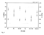
図1は、少なくとも1つのCrTaN層を有する種々の層系のナノ硬度Hとヤング率Eの値を示す。 FIG. 1 shows the values of nanohardness H and Young's modulus E for various layer systems with at least one CrTaN layer.
ここで、ナノ硬度は、バーコヴィッチダイアモンド圧子を有するナノインデンター(ウルトラ マイクロ インデンテーション システム‐UMIS)で測定された。各試料当たり16個の圧子が測定ごとに使用され、ナノ硬度及びヤング率が求められた。 Here, the nanohardness was measured with a nanoindenter (Ultra Micro Indentation System - UMIS) with a Berkovich diamond indenter. Sixteen indenters per sample were used per measurement to determine nanohardness and Young's modulus.
図1から直ちに判ることは、それぞれCrTaN層を含む単層SL及び二重層BLに比して、多層被膜系MLを使用することにより顕著な硬度の上昇が生じることである。16.0~15.5GPaのナノ硬度を有するSL及びBL試料から出発して、ML試料におけるナノ硬度は約25~30GPaに上昇する。 It can be readily seen from FIG. 1 that a significant increase in hardness occurs by using the multi-layer coating system ML compared to the single-layer SL and double-layer BL, each containing a CrTaN layer. Starting from SL and BL samples with nanohardness of 16.0-15.5 GPa, the nanohardness in ML samples increases to about 25-30 GPa.
図1に示した結果から判明するのは、多層被膜系MLが単層SL及び二重層BLに比して、より高い硬度と従って改良された耐摩耗性を有することである。 It can be seen from the results shown in FIG. 1 that the multilayer coating system ML has a higher hardness and thus improved wear resistance compared to the single-layer SL and double-layer BL.
また、AlTiN被膜、特にRef.1-PM層及びRef.2-CC層に比して、同様に図1に示すように、より高いナノ硬度を達成できる。 AlTiN coatings, especially Ref. 1-PM layer and Ref. Compared to the 2-CC layer, a higher nanohardness can be achieved, also shown in FIG.
CrTaN及びAlTiNから成る多層被膜系の構造は、これらの材料から成る単層又は二重層に比して硬度の向上を生じる。 The construction of multilayer coating systems consisting of CrTaN and AlTiN results in improved hardness compared to single or double layers of these materials.
更に、多層被膜系では、例えば単層被膜に見られるような、また、文献に記載されているような、CrTaNのCr2N及びTa2Nへの熱分解が大幅に抑制されることが分かる。従って、提案された多層被膜系から高温使用に特に適した被膜系が生じる。多層被膜系では、立方晶結晶構造の安定化に基づき熱分解が防止されるので、形成された層は熱的に安定でもあり、これにより比較的長い動作寿命が可能となる。この特性プロフィルは、従って、硬質金属スローアウェイチップ並びに超硬合金工具においても、摩耗保護層としての使用に適切である。 Furthermore, it can be seen that the multilayer coating system greatly inhibits the thermal decomposition of CrTaN to Cr2N and Ta2N , as seen for example in monolayer coatings and described in the literature. . The proposed multilayer coating system thus results in a coating system that is particularly suitable for high temperature applications. In multilayer coating systems, the layers formed are also thermally stable, since thermal decomposition is prevented due to the stabilization of the cubic crystal structure, which allows a relatively long operating life. This property profile is therefore suitable for use as a wear protection layer in hard metal indexable inserts as well as in cemented carbide tools.
更にトライボメーター試験(室温、500℃、700℃)において多層被膜系MLの摩擦値がより小さいことが確認された。 Furthermore, tribometer tests (room temperature, 500° C., 700° C.) confirmed lower friction values for the multilayer system ML.
このためCSM インスツルメンツ社のピン・ディスクタイプの直径6mmのAl2O3製の対向体を有するトライボメーターが使用され、室温、500℃及び700℃で測定が行なわれた。設定負荷は5N、滑動行程300m、速度10cm/秒であった。摩耗溝の半径は5mmであった。摩耗溝の測定はヴィーコ社の白光プロフィロメータにより行なわれ、2D横断面及び3D表示が設定された。 For this purpose a tribometer of the pin-disc type from CSM Instruments with a 6 mm diameter Al 2 O 3 counterbody was used and measurements were carried out at room temperature, 500°C and 700°C. The set load was 5 N, the sliding stroke was 300 m, and the speed was 10 cm/sec. The radius of the wear groove was 5 mm. Wear groove measurements were made with a white light profilometer from Vico, setting up a 2D cross-section and a 3D representation.
上述の試料の測定結果は下記の表6に示されている。すぐに判ることは、多層被覆系MLの達成可能な摩擦値(摩擦係数μ)は≦0.7であり、最良の場合は≦0.6ですらあることである。従って、多層被覆系MLを有する試料は、摩擦値が低くなければならない工具、例えば、ねじ用工具、リーマー及び超硬合金工具、に対して特に好適である。 The measurement results of the above samples are shown in Table 6 below. It is readily apparent that the achievable friction values (coefficient of friction μ) of multilayer coating systems ML are ≤0.7 and even ≤0.6 in the best case. Samples with the multilayer coating system ML are therefore particularly suitable for tools which must have low friction values, such as screw tools, reamers and cemented carbide tools.
表6:測定された摩擦係数及び摩耗係数

更に層系の固有応力値が下記の表7にリストアップされている。この場合、応力は、「成膜直後」の状態でシリコン試料のウエハ曲率法で求められた。被膜の製法次第でこれらの値は勿論変化し得る。 Further intrinsic stress values for the layer system are listed in Table 7 below. In this case, the stress was determined by the wafer curvature method on silicon samples in the "as-deposited" state. These values can of course vary depending on the method of manufacturing the coating.
表7:Si試料におけるウエハ曲率法で測定された層固有応力

多層被覆系は比較的低い被膜固有応力を有することも判明しており、これにより動作寿命及び稼働期間にも更に有利な影響が生じる。 Multi-layer coating systems have also been found to have relatively low intrinsic coating stresses, which also has a more beneficial impact on operational life and duration.
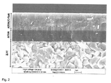
多層被覆系MLの構造の一例を図2の破断図に示すが、ここでは硬質金属基材の上にAlTiN基層が設けられており、この上にAlTiN/CrTaN多層被覆系が施されている。 An example of the structure of the multilayer coating system ML is shown in the cutaway view of FIG. 2, where a hard metal substrate is provided with an AlTiN substrate, on which the AlTiN/CrTaN multilayer coating system is applied.
従って、上述の多層被覆系MLの場合、かなりの硬度の向上が見られ、同時に摩擦値が低く耐久時間が長い。 Thus, in the case of the multilayer coating system ML described above, a considerable increase in hardness is observed, while at the same time the friction values are low and the service life is long.
多層被膜系MLの使用時の切削実験では、被膜は、摩擦値が低くなければならず同時に高い硬度が要求されるねじ用工具、リーマー及び超硬合金工具に特に有利であることが実証されている。 Cutting experiments when using the multilayer coating system ML have demonstrated that the coating is particularly advantageous for screw tools, reamers and cemented carbide tools where low friction values are required and at the same time high hardness is required. there is
図3には種々の多層被膜系についての切削試験の測定結果が示されている。この場合、湿式フライスにおけるフライス機の切削インサートの動作寿命が分単位で示されている。切削試験は具体的には以下の試験パラメータで実施された。 FIG. 3 shows the results of cutting test measurements for various multilayer coating systems. In this case, the working life of the cutting insert of the milling machine in wet milling is given in minutes. Specifically, the cutting test was performed with the following test parameters.
単歯による同期フライス、ブロック面をスパイラル上に行送り。材料としてSP300高張力鋼を使用し、工具はスローアウェイチップの収容用にISCAR F45ST D050-22で、SK50工具ホルダに入れられた。被加工材は、寸法が400x200x96mmで強度は1,000N/mm2であった。フライス機は、直径50mm、迎角45°、切削速度Vc=250m/min(乾式)、150m/min(湿式)、1刃当り送りfz=0.25mm、切込み深さap=32mmで推進した。 Synchronous milling with single tooth, spiral feed on block face. SP300 high-strength steel was used as the material and the tool was ISCAR F45ST D050-22 to accommodate the indexable insert and was placed in an SK50 tool holder. The workpiece had dimensions of 400×200×96 mm and a strength of 1,000 N/mm 2 . The milling machine was propelled with a diameter of 50 mm, angle of attack of 45°, cutting speed Vc = 250 m/min (dry), 150 m/min (wet), feed per tooth fz = 0.25 mm, depth of cut ap = 32 mm.
図3から直ちに判明することは、多層被覆系MLが最良の動作寿命を有することである。湿式加工では参照層系に対し動作寿命が約20%改良されたことが判明している。図示していない乾式加工では、多層被覆系MLは、参照層系に対しそれほど改良されていない。 It is immediately apparent from FIG. 3 that the multilayer coating system ML has the best operating lifetime. Wet processing has been found to improve operating life by about 20% over the reference layer system. In dry processing, not shown, the multilayer coating system ML is not significantly improved over the reference layer system.
更に、適当な基材、有利には所定の形状の硬質金属基材を有する切削装置用の切削工具を作ることもできる。この切削工具は、例えば旋盤及びフライス装置用の刃体の形で又はスローアウェイチップの形で使用することができる。 Furthermore, it is also possible to make cutting tools for cutting machines with a suitable substrate, preferably a hard metal substrate of predetermined shape. The cutting tool can be used, for example, in the form of cutting bodies for lathes and milling machines or in the form of indexable inserts.
この基材上に、交互にCrTaNとAlTiNとから成る多層被覆系を有する硬質材料層が、上述のやり方で、僅かな層厚で施される。 A hard material layer with a multilayer coating system consisting of alternating CrTaN and AlTiN is applied to this substrate in the manner described above with a low layer thickness.
更に、表面構造及び/又は表面粗さを各用途に適合させるために、硬質材料層を後処理することができる。この後処理は、例えば湿式噴射、乾式噴射及び/又は着色により実施することができる。被覆層及び/又は機能被膜を施す場合には、これらの被膜をも後処理することができる。 Furthermore, the hard material layer can be post-treated in order to adapt the surface structure and/or surface roughness to the respective application. This aftertreatment can be carried out, for example, by wet-jetting, dry-jetting and/or coloring. If cover layers and/or functional coatings are applied, these coatings can also be post-treated.
以下にCrTa複合ターゲットの形の被膜源の製造について説明するが、この被膜源は、上述の硬質材料層の製造方法においてCrTaN被膜をPVDにより堆積するのに有利に使用された。 The following describes the production of a coating source in the form of a CrTa composite target, which was advantageously used to deposit a CrTaN coating by PVD in the method for producing the hard material layer described above.
複合ターゲットの製造のため、まず純Crと純Ta粉末が原材料として用意される。粉末の粒径は、それぞれ45μm以下であると有利である。両粉末は、粉末から作られるCrTa複合ターゲットの所望の比で且つできるだけ互いに均質に混合される。小さい粒径のおかげで、両粉末の混合は特に均質に用意することができ、これに続く高密度化工程ではターゲット中に微細分布したTaCr2相を形成させることができる。 To manufacture the composite target, pure Cr and pure Ta powders are first prepared as raw materials. Advantageously, the particle sizes of the powders are each less than or equal to 45 μm. Both powders are mixed with each other as homogeneously as possible in the desired ratio of the CrTa composite target made from the powders. Thanks to the small particle size, a particularly homogeneous mixture of both powders can be prepared and the subsequent densification step can lead to the formation of a finely distributed TaCr 2 phase in the target.
上述のように、製造すべきCrTa複合ターゲットの混合物中において、Ta含有量が1~60原子%、特に有利には20~30原子%、更に特に有利には25原子%とされる。 As mentioned above, the mixture of the CrTa composite target to be produced has a Ta content of 1 to 60 atomic %, particularly preferably 20 to 30 atomic %, very particularly preferably 25 atomic %.
次いで、ほぼ均質の粉末混合物からプレス型内で焼結工程により、CrTa複合ターゲットが作られる。焼結工程は、例えばホットプレス、直接通電型プレス(例えば、スパーク・プラズマ焼結(SPS))、又は熱間等圧プレス(HIP)により、実施される。この場合、粉末は、室内で、プレス中に、加熱導体により又は直接電流により及び/又は誘導加熱により、処理できる。 A CrTa composite target is then made from the substantially homogeneous powder mixture by a sintering process in a press die. The sintering process is performed, for example, by hot pressing, direct current pressing (eg, spark plasma sintering (SPS) ), or hot isostatic pressing (HIP). In this case, the powder can be treated indoors, during pressing, by heating conductors or by direct electric current and/or by induction heating.
CrTa複合ターゲットを作るためのSPS又はホットプレスによる焼結は、1,100~1,750℃の温度範囲、有利には1,300~1,500℃の温度範囲、で行なわれる。焼結時間は、再結晶を回避し組成の微粒性を維持するためにできるだけ短く、有利には1時間未満とされる。 The sintering by SPS or hot pressing to make CrTa composite targets is carried out in a temperature range of 1,100-1,750°C, preferably in a temperature range of 1,300-1,500°C. The sintering time is kept as short as possible, preferably less than 1 hour, to avoid recrystallization and maintain the fine-grained nature of the composition.
図4は、このようにして作られた複合ターゲットによる粒界エッチングによる金属組織断面図を示す。焼結工程後の組成は3つの相、即ち純Cr又はCr混合結晶の相1、純Ta又はTa混合結晶の相2、及びTaCr2の相3から成る。TaCr2相3は、TaからCrへの移行の境界面にある。CrTa複合ターゲットを提案されたように用意するためには、上述の3つの相が全て存在しなければならない。対応する相ダイアグラムは図5に示されている。
FIG. 4 shows a cross-sectional view of the metallographic structure by grain boundary etching with a composite target thus produced. The composition after the sintering process consists of three phases:
焼結後に測定された密度は、理論密度の少なくとも90%、有利には95%又は98%である。 The density measured after sintering is at least 90%, preferably 95% or 98% of the theoretical density.
このようにして作られたCrTa複合ターゲットは、直接使用するか又は操作性を良くするために、その裏面でバッキングプレートに、例えば接着、硬ろう付け又は拡散接着により、固定することができ、これによりターゲットはPVD設備においてCrTaNの堆積のために固定することができる。また複数のCrTa複合ターゲットを単一のバッキングプレートに固定し、例えばPVD設備中の所望の配置を考慮することができる。 The CrTa composite target thus made can be used directly or fixed on its underside to a backing plate for better handling, for example by gluing, hard brazing or diffusion bonding, which allows the target to be fixed for the deposition of CrTaN in a PVD facility. Also, multiple CrTa composite targets can be secured to a single backing plate to allow for desired placement in, for example, a PVD facility.
個々の実施例で説明した全ての個々の特徴は、適用可能であれば、本発明の範囲を逸脱することなしに互いに組み合わせるか交換することができる。 All individual features described in individual embodiments, where applicable, can be combined or exchanged with one another without departing from the scope of the invention.
1 Cr又はCr混合結晶相
2 Ta又はTa混合結晶相
3 TaCr2相
1 Cr or Cr
Claims (20)
AlTiNが、原子組成AlxTi1-xN(0.2≦x≦0.9)で基材上に施され、
CrTaNが原子組成Cr1-yTayN(0.01≦y≦0.65)で基材上に施され、
前記多層被膜系の個々の層が、5~200ナノメータの厚さで堆積され、ここで、10~5,000の数の層が交互に堆積される、
方法。 A method for producing a hard material layer on a substrate, characterized in that a multilayer coating system is applied on the substrate by alternately depositing CrTaN and AlTiN by physical vapor deposition (PVD). hand,
AlTiN is applied onto the substrate with an atomic composition Al x Ti 1-x N (0.2≦x≦0.9);
CrTaN is applied onto the substrate with an atomic composition Cr 1-y Ta y N (0.01≦y≦0.65);
The individual layers of said multilayer coating system are deposited with a thickness of 5 to 200 nanometers, wherein the layers are alternately deposited with a number of 10 to 5,000.
Method.
前記AlTiN層の原子組成はAl The atomic composition of the AlTiN layer is Al xx TiTi 1-x1-x N(0.2≦x≦0.9)であり、N (0.2 ≤ x ≤ 0.9),
前記CrTaN層の原子組成はCr The atomic composition of the CrTaN layer is Cr 1-y1-y TaTa yy N(0.01≦y≦0.65)であり、N (0.01 ≤ y ≤ 0.65),
前記CrTaN層および前記AlTiN層の個々の層が、5~200ナノメータの厚さであり、10~5,000の数の層が交互に堆積されている、 The individual layers of said CrTaN layer and said AlTiN layer are between 5 and 200 nanometers thick, and the number of layers between 10 and 5,000 are alternately deposited.
硬質材料層。Hard material layer.
AlTiNが、原子組成AlxTi1-xN(0.2≦x≦0.9)であり、
CrTaNが、原子組成Cr1-yTayN(0.01≦y≦0.65)であり、
前記多層被膜系の個々の層が、5~200ナノメータの厚さであり、ここで、10~5,000の数の層が交互に堆積されている、
切削工具。 A cutting tool with a substrate made of a hard metal, characterized in that the multilayer coating system comprises alternating CrTaN and AlTiN layers deposited on the substrate by physical vapor deposition (PVD), ,
AlTiN has an atomic composition Al x Ti 1-x N (0.2≦x≦0.9),
CrTaN has an atomic composition Cr 1-y Ta y N (0.01≦y≦0.65),
the individual layers of said multilayer coating system are between 5 and 200 nanometers thick, wherein the number of layers between 10 and 5,000 are alternately deposited;
Cutting tools.
Applications Claiming Priority (3)
| Application Number | Priority Date | Filing Date | Title |
|---|---|---|---|
| ATGM49/2016U AT15220U1 (en) | 2016-03-07 | 2016-03-07 | Process for producing a hard material layer on a substrate, hard material layer, cutting tool and coating source |
| ATGM49/2016 | 2016-03-07 | ||
| PCT/AT2017/000010 WO2017152196A1 (en) | 2016-03-07 | 2017-03-03 | Method for producing a hard material layer on a substrate, hard material layer, machining tool and coating source |
Publications (3)
| Publication Number | Publication Date |
|---|---|
| JP2019509399A JP2019509399A (en) | 2019-04-04 |
| JP2019509399A5 JP2019509399A5 (en) | 2020-03-05 |
| JP7112330B2 true JP7112330B2 (en) | 2022-08-03 |
Family
ID=58264126
Family Applications (1)
| Application Number | Title | Priority Date | Filing Date |
|---|---|---|---|
| JP2018546658A Active JP7112330B2 (en) | 2016-03-07 | 2017-03-03 | Method for producing hard material layers on substrates, hard material layers, cutting tools and coating sources |
Country Status (6)
| Country | Link |
|---|---|
| US (1) | US10920325B2 (en) |
| EP (2) | EP3929325A1 (en) |
| JP (1) | JP7112330B2 (en) |
| CN (1) | CN108884551A (en) |
| AT (1) | AT15220U1 (en) |
| WO (1) | WO2017152196A1 (en) |
Families Citing this family (8)
| Publication number | Priority date | Publication date | Assignee | Title |
|---|---|---|---|---|
| JP6814758B2 (en) * | 2018-02-19 | 2021-01-20 | 山陽特殊製鋼株式会社 | Sputtering target |
| JP7274121B2 (en) * | 2019-03-05 | 2023-05-16 | 三菱マテリアル株式会社 | A surface-coated cutting tool with a hard coating layer that exhibits excellent wear resistance and peeling resistance. |
| US10484940B1 (en) * | 2019-05-21 | 2019-11-19 | Motorola Mobility Llc | Network association based on network performance capabilities |
| CN111441024A (en) * | 2020-04-29 | 2020-07-24 | 金堆城钼业股份有限公司 | Tungsten surface oxygen-blocking film and preparation method thereof |
| CN112296356B (en) * | 2020-10-28 | 2022-11-04 | 湖南华曙高科技股份有限公司 | High-rise thick sintering method and equipment for selective laser sintering |
| CN112276111B (en) * | 2020-10-28 | 2022-11-01 | 湖南华曙高科技股份有限公司 | High-layer thick low-temperature sintering method and equipment for selective laser sintering |
| CN112247145B (en) * | 2020-10-28 | 2022-11-04 | 湖南华曙高科技股份有限公司 | Indirect forming method and device for preparing metal parts |
| CN112264619B (en) * | 2020-10-28 | 2022-11-01 | 湖南华曙高科技股份有限公司 | Indirect forming method for preparing metal product |
Citations (7)
| Publication number | Priority date | Publication date | Assignee | Title |
|---|---|---|---|---|
| JP2001277010A (en) | 2000-03-29 | 2001-10-09 | Ngk Spark Plug Co Ltd | Coated tool |
| JP2003326415A (en) | 2002-03-20 | 2003-11-18 | Seco Tools Ab | Cutting tool insert, method for manufacturing the insert, and milling method using the insert |
| JP2008093760A (en) | 2006-10-10 | 2008-04-24 | Nachi Fujikoshi Corp | Hard coating exhibiting excellent performance in dry machining |
| JP2008279563A (en) | 2007-05-11 | 2008-11-20 | Sumitomo Electric Ind Ltd | Surface-coated cutting tool |
| JP2012130948A (en) | 2010-12-22 | 2012-07-12 | Sumitomo Electric Ind Ltd | Rotating tool |
| CN102978576A (en) | 2012-12-03 | 2013-03-20 | 苏州晶纯新材料有限公司 | Production method for high-compactness chromium alloy target |
| JP2014077201A (en) | 2006-10-10 | 2014-05-01 | Oerlikon Trading Truebbach | Coating system having at least one double oxide mixed crystal coating |
Family Cites Families (13)
| Publication number | Priority date | Publication date | Assignee | Title |
|---|---|---|---|---|
| JPH10133216A (en) | 1996-11-01 | 1998-05-22 | Hitachi Ltd | Active matrix type liquid crystal display device |
| KR100846384B1 (en) * | 2002-06-29 | 2008-07-15 | 주식회사 하이닉스반도체 | Method for fabricating semiconductor device |
| US20090186230A1 (en) * | 2007-10-24 | 2009-07-23 | H.C. Starck Inc. | Refractory metal-doped sputtering targets, thin films prepared therewith and electronic device elements containing such films |
| US7947363B2 (en) * | 2007-12-14 | 2011-05-24 | Kennametal Inc. | Coated article with nanolayered coating scheme |
| WO2010007958A1 (en) | 2008-07-14 | 2010-01-21 | 株式会社タンガロイ | Coated member |
| IT1397559B1 (en) * | 2010-01-15 | 2013-01-16 | Scattolon | PERFECTED MOLD FOR BENDING THE SHEET |
| WO2011131460A2 (en) * | 2010-04-23 | 2011-10-27 | Sulzer Metaplas Gmbh | Pvd coating for metal machining |
| CN102560344A (en) * | 2010-12-24 | 2012-07-11 | 鸿富锦精密工业(深圳)有限公司 | Hard thin film, product provided with same, and production method of product |
| JP2013221215A (en) * | 2012-04-19 | 2013-10-28 | Ihi Corp | Surface coated member and method for manufacturing the same, and method for coating the surface coated member |
| US9103036B2 (en) * | 2013-03-15 | 2015-08-11 | Kennametal Inc. | Hard coatings comprising cubic phase forming compositions |
| WO2015034203A1 (en) | 2013-09-09 | 2015-03-12 | 한국야금 주식회사 | Hard coating film for cutting tools |
| CN115094390A (en) * | 2014-09-30 | 2022-09-23 | 捷客斯金属株式会社 | Master alloy for sputtering target and method for producing sputtering target |
| JP6814758B2 (en) * | 2018-02-19 | 2021-01-20 | 山陽特殊製鋼株式会社 | Sputtering target |
-
2016
- 2016-03-07 AT ATGM49/2016U patent/AT15220U1/en unknown
-
2017
- 2017-03-03 WO PCT/AT2017/000010 patent/WO2017152196A1/en active Application Filing
- 2017-03-03 CN CN201780015393.5A patent/CN108884551A/en active Pending
- 2017-03-03 EP EP21189586.7A patent/EP3929325A1/en active Pending
- 2017-03-03 US US16/083,058 patent/US10920325B2/en active Active
- 2017-03-03 EP EP17718326.6A patent/EP3426816A1/en active Pending
- 2017-03-03 JP JP2018546658A patent/JP7112330B2/en active Active
Patent Citations (7)
| Publication number | Priority date | Publication date | Assignee | Title |
|---|---|---|---|---|
| JP2001277010A (en) | 2000-03-29 | 2001-10-09 | Ngk Spark Plug Co Ltd | Coated tool |
| JP2003326415A (en) | 2002-03-20 | 2003-11-18 | Seco Tools Ab | Cutting tool insert, method for manufacturing the insert, and milling method using the insert |
| JP2008093760A (en) | 2006-10-10 | 2008-04-24 | Nachi Fujikoshi Corp | Hard coating exhibiting excellent performance in dry machining |
| JP2014077201A (en) | 2006-10-10 | 2014-05-01 | Oerlikon Trading Truebbach | Coating system having at least one double oxide mixed crystal coating |
| JP2008279563A (en) | 2007-05-11 | 2008-11-20 | Sumitomo Electric Ind Ltd | Surface-coated cutting tool |
| JP2012130948A (en) | 2010-12-22 | 2012-07-12 | Sumitomo Electric Ind Ltd | Rotating tool |
| CN102978576A (en) | 2012-12-03 | 2013-03-20 | 苏州晶纯新材料有限公司 | Production method for high-compactness chromium alloy target |
Non-Patent Citations (1)
| Title |
|---|
| Yung -I Chen, 他,Preparation and annealing study of CrTaN coatings Technology on WC-Co,Surface & Coatings Technology,vol.206,2011年06月17日,p.1640 - p.1647,doi:10.1016/j.surfcoat.2011.06.012 |
Also Published As
| Publication number | Publication date |
|---|---|
| WO2017152196A1 (en) | 2017-09-14 |
| EP3929325A1 (en) | 2021-12-29 |
| JP2019509399A (en) | 2019-04-04 |
| US20190062924A1 (en) | 2019-02-28 |
| EP3426816A1 (en) | 2019-01-16 |
| US10920325B2 (en) | 2021-02-16 |
| CN108884551A (en) | 2018-11-23 |
| AT15220U1 (en) | 2017-03-15 |
Similar Documents
| Publication | Publication Date | Title |
|---|---|---|
| JP7112330B2 (en) | Method for producing hard material layers on substrates, hard material layers, cutting tools and coating sources | |
| EP3269479B1 (en) | Surface-coated cutting tool and method for manufacturing same | |
| KR101685446B1 (en) | Cutting tool | |
| KR20150045425A (en) | Surface-coated cutting tool | |
| JP4748450B2 (en) | A surface-coated cutting tool that exhibits excellent chipping resistance with a hard coating layer in high-speed intermittent cutting | |
| JP2010099735A (en) | Coated die for plastic working | |
| CN108998758A (en) | Has cated drill bit | |
| JP3460288B2 (en) | Surface coating member with excellent wear resistance | |
| JP4793750B2 (en) | Surface coated cermet cutting tool with excellent chipping resistance in high-speed intermittent cutting of hard steel with excellent hard coating layer | |
| CN112055632B (en) | Coated cutting tool and method for manufacturing same | |
| JP5035980B2 (en) | Surface-coated cutting tool that exhibits high wear resistance with a hard coating layer in high-speed milling and a method for producing the same | |
| CN114761606B (en) | Cutting tool with hard coating film formed thereon | |
| JP5035979B2 (en) | Surface-coated cutting tool that exhibits high wear resistance with a hard coating layer in high-speed milling and a method for producing the same | |
| JP2008229759A (en) | Surface-coated cutting tool having hard coat layer exhibiting excellent chipping resistance and wear resistance during high-speed cutting, and its manufacturing method | |
| JP4645820B2 (en) | Cutting tool made of surface-coated cemented carbide that provides excellent wear resistance with a hard coating layer in high-speed cutting of hardened steel | |
| JP4244379B2 (en) | Surface coated cemented carbide cutting tool with excellent wear resistance with high surface coating layer in high speed cutting | |
| JP2008049454A (en) | Surface coated cutting tool having hard coating layer showing superior chipping resistance and wear resistance | |
| CN112805109A (en) | Cutting tool and method for manufacturing same | |
| CN112262007B (en) | Cutting tool | |
| JP2009279694A (en) | Surface-coated cutting tool having hard coating layer exhibiting excellent chipping resistance and wear resistance in high-speed heavy cutting | |
| JP2010105137A (en) | Surface-coated cutting tool | |
| JP2008260097A (en) | Surface-coated cutting tool | |
| JP2008173750A (en) | Surface-coated cutting tool provided with hard coated layer achieving excellent wear resistance in high speed cutting | |
| JP2008049455A (en) | Surface coated cutting tool having hard coating layer showing superior chipping resistance and wear resistance | |
| CN112262006A (en) | Cutting tool |
Legal Events
| Date | Code | Title | Description |
|---|---|---|---|
| A521 | Request for written amendment filed |
Free format text: JAPANESE INTERMEDIATE CODE: A523 Effective date: 20200120 |
|
| A621 | Written request for application examination |
Free format text: JAPANESE INTERMEDIATE CODE: A621 Effective date: 20200120 |
|
| A977 | Report on retrieval |
Free format text: JAPANESE INTERMEDIATE CODE: A971007 Effective date: 20210120 |
|
| A131 | Notification of reasons for refusal |
Free format text: JAPANESE INTERMEDIATE CODE: A131 Effective date: 20210216 |
|
| A601 | Written request for extension of time |
Free format text: JAPANESE INTERMEDIATE CODE: A601 Effective date: 20210517 |
|
| RD03 | Notification of appointment of power of attorney |
Free format text: JAPANESE INTERMEDIATE CODE: A7423 Effective date: 20210517 |
|
| A601 | Written request for extension of time |
Free format text: JAPANESE INTERMEDIATE CODE: A601 Effective date: 20210715 |
|
| A521 | Request for written amendment filed |
Free format text: JAPANESE INTERMEDIATE CODE: A523 Effective date: 20210816 |
|
| A131 | Notification of reasons for refusal |
Free format text: JAPANESE INTERMEDIATE CODE: A131 Effective date: 20220118 |
|
| A521 | Request for written amendment filed |
Free format text: JAPANESE INTERMEDIATE CODE: A523 Effective date: 20220414 |
|
| TRDD | Decision of grant or rejection written | ||
| A01 | Written decision to grant a patent or to grant a registration (utility model) |
Free format text: JAPANESE INTERMEDIATE CODE: A01 Effective date: 20220712 |
|
| A61 | First payment of annual fees (during grant procedure) |
Free format text: JAPANESE INTERMEDIATE CODE: A61 Effective date: 20220722 |
|
| R150 | Certificate of patent or registration of utility model |
Ref document number: 7112330 Country of ref document: JP Free format text: JAPANESE INTERMEDIATE CODE: R150 |