JP7111140B2 - semiconductor equipment - Google Patents

semiconductor equipment Download PDF

Info

Publication number
JP7111140B2
JP7111140B2 JP2020158041A JP2020158041A JP7111140B2 JP 7111140 B2 JP7111140 B2 JP 7111140B2 JP 2020158041 A JP2020158041 A JP 2020158041A JP 2020158041 A JP2020158041 A JP 2020158041A JP 7111140 B2 JP7111140 B2 JP 7111140B2
Authority
JP
Japan
Prior art keywords
wire
electrode
semiconductor element
bonding
wiring member
Prior art date
Legal status (The legal status is an assumption and is not a legal conclusion. Google has not performed a legal analysis and makes no representation as to the accuracy of the status listed.)
Active
Application number
JP2020158041A
Other languages
Japanese (ja)
Other versions
JP2021061393A5 (en
JP2021061393A (en
Inventor
大輔 福岡
知巳 奥村
祐司 大谷
渉 小林
匠 野村
智明 満永
敬洋 平野
孝充 坂井
賢吾 岡
Current Assignee (The listed assignees may be inaccurate. Google has not performed a legal analysis and makes no representation or warranty as to the accuracy of the list.)
Denso Corp
Original Assignee
Denso Corp
Priority date (The priority date is an assumption and is not a legal conclusion. Google has not performed a legal analysis and makes no representation as to the accuracy of the date listed.)
Filing date
Publication date
Application filed by Denso Corp filed Critical Denso Corp
Priority to PCT/JP2020/036372 priority Critical patent/WO2021065736A1/en
Priority to CN202080069629.5A priority patent/CN114503255A/en
Publication of JP2021061393A publication Critical patent/JP2021061393A/en
Publication of JP2021061393A5 publication Critical patent/JP2021061393A5/ja
Priority to US17/708,525 priority patent/US20220223544A1/en
Application granted granted Critical
Publication of JP7111140B2 publication Critical patent/JP7111140B2/en
Active legal-status Critical Current
Anticipated expiration legal-status Critical

Links

Images

Classifications

    • HELECTRICITY
    • H01ELECTRIC ELEMENTS
    • H01LSEMICONDUCTOR DEVICES NOT COVERED BY CLASS H10
    • H01L2224/00Indexing scheme for arrangements for connecting or disconnecting semiconductor or solid-state bodies and methods related thereto as covered by H01L24/00
    • H01L2224/01Means for bonding being attached to, or being formed on, the surface to be connected, e.g. chip-to-package, die-attach, "first-level" interconnects; Manufacturing methods related thereto
    • H01L2224/02Bonding areas; Manufacturing methods related thereto
    • H01L2224/04Structure, shape, material or disposition of the bonding areas prior to the connecting process
    • H01L2224/06Structure, shape, material or disposition of the bonding areas prior to the connecting process of a plurality of bonding areas
    • H01L2224/0601Structure
    • H01L2224/0603Bonding areas having different sizes, e.g. different heights or widths
    • HELECTRICITY
    • H01ELECTRIC ELEMENTS
    • H01LSEMICONDUCTOR DEVICES NOT COVERED BY CLASS H10
    • H01L2224/00Indexing scheme for arrangements for connecting or disconnecting semiconductor or solid-state bodies and methods related thereto as covered by H01L24/00
    • H01L2224/01Means for bonding being attached to, or being formed on, the surface to be connected, e.g. chip-to-package, die-attach, "first-level" interconnects; Manufacturing methods related thereto
    • H01L2224/26Layer connectors, e.g. plate connectors, solder or adhesive layers; Manufacturing methods related thereto
    • H01L2224/31Structure, shape, material or disposition of the layer connectors after the connecting process
    • H01L2224/32Structure, shape, material or disposition of the layer connectors after the connecting process of an individual layer connector
    • H01L2224/321Disposition
    • H01L2224/32151Disposition the layer connector connecting between a semiconductor or solid-state body and an item not being a semiconductor or solid-state body, e.g. chip-to-substrate, chip-to-passive
    • H01L2224/32221Disposition the layer connector connecting between a semiconductor or solid-state body and an item not being a semiconductor or solid-state body, e.g. chip-to-substrate, chip-to-passive the body and the item being stacked
    • H01L2224/32245Disposition the layer connector connecting between a semiconductor or solid-state body and an item not being a semiconductor or solid-state body, e.g. chip-to-substrate, chip-to-passive the body and the item being stacked the item being metallic
    • HELECTRICITY
    • H01ELECTRIC ELEMENTS
    • H01LSEMICONDUCTOR DEVICES NOT COVERED BY CLASS H10
    • H01L2224/00Indexing scheme for arrangements for connecting or disconnecting semiconductor or solid-state bodies and methods related thereto as covered by H01L24/00
    • H01L2224/73Means for bonding being of different types provided for in two or more of groups H01L2224/10, H01L2224/18, H01L2224/26, H01L2224/34, H01L2224/42, H01L2224/50, H01L2224/63, H01L2224/71
    • H01L2224/732Location after the connecting process
    • H01L2224/73251Location after the connecting process on different surfaces
    • H01L2224/73265Layer and wire connectors
    • HELECTRICITY
    • H01ELECTRIC ELEMENTS
    • H01LSEMICONDUCTOR DEVICES NOT COVERED BY CLASS H10
    • H01L2224/00Indexing scheme for arrangements for connecting or disconnecting semiconductor or solid-state bodies and methods related thereto as covered by H01L24/00
    • H01L2224/80Methods for connecting semiconductor or other solid state bodies using means for bonding being attached to, or being formed on, the surface to be connected
    • H01L2224/83Methods for connecting semiconductor or other solid state bodies using means for bonding being attached to, or being formed on, the surface to be connected using a layer connector
    • H01L2224/8312Aligning
    • H01L2224/83136Aligning involving guiding structures, e.g. spacers or supporting members
    • H01L2224/83138Aligning involving guiding structures, e.g. spacers or supporting members the guiding structures being at least partially left in the finished device
    • H01L2224/8314Guiding structures outside the body
    • HELECTRICITY
    • H01ELECTRIC ELEMENTS
    • H01LSEMICONDUCTOR DEVICES NOT COVERED BY CLASS H10
    • H01L2224/00Indexing scheme for arrangements for connecting or disconnecting semiconductor or solid-state bodies and methods related thereto as covered by H01L24/00
    • H01L2224/80Methods for connecting semiconductor or other solid state bodies using means for bonding being attached to, or being formed on, the surface to be connected
    • H01L2224/83Methods for connecting semiconductor or other solid state bodies using means for bonding being attached to, or being formed on, the surface to be connected using a layer connector
    • H01L2224/8319Arrangement of the layer connectors prior to mounting
    • H01L2224/83192Arrangement of the layer connectors prior to mounting wherein the layer connectors are disposed only on another item or body to be connected to the semiconductor or solid-state body
    • HELECTRICITY
    • H01ELECTRIC ELEMENTS
    • H01LSEMICONDUCTOR DEVICES NOT COVERED BY CLASS H10
    • H01L2924/00Indexing scheme for arrangements or methods for connecting or disconnecting semiconductor or solid-state bodies as covered by H01L24/00
    • H01L2924/15Details of package parts other than the semiconductor or other solid state devices to be connected
    • H01L2924/181Encapsulation

Description

この明細書における開示は、半導体装置に関する。 The disclosure in this specification relates to semiconductor devices.

特許文献1は、はんだ厚を確保するNiボールを開示する。先行技術文献の記載内容は、この明細書における技術的要素の説明として、参照により援用される。 Patent Literature 1 discloses a Ni ball that ensures solder thickness. The contents of the prior art documents are incorporated by reference as descriptions of technical elements in this specification.

特許第5510623号公報Japanese Patent No. 5510623

Niボールは、適用対象が限定される。たとえばソルダダイボンドの場合、Niボールは、はんだの溶融炉内において少なからず溶ける。よって、はんだ(接合部材)の最低保証厚みを確保できない虞がある。上述の観点において、または言及されていない他の観点において、半導体装置にはさらなる改良が求められている。 Ni balls are limited in application. For example, in the case of solder die bonding, Ni balls are not a little melted in a solder melting furnace. Therefore, there is a possibility that the minimum guaranteed thickness of the solder (joining member) cannot be ensured. In view of the above or in other aspects not mentioned, semiconductor devices are desired to be further improved.

開示されるひとつの目的は、信頼性の高い半導体装置を提供することにある。 One object of the disclosure is to provide a highly reliable semiconductor device.

ここに開示された半導体装置は、主電極として、表面に形成された表面電極(31)と、板厚方向において表面とは反対の裏面に形成され、表面電極よりも面積の大きい裏面電極(32)と、を有する半導体素子(30)と、第1対向面と第2対向面との間に介在して接合部を形成する接合部材と、接合部材を介して主電極と電気的に接続された配線部材と、接合部材内に配置され、第1対向面に固定されて第1対向面から突起する複数のワイヤ片(90)と、を備え、配線部材は、裏面側に配置され、裏面電極と接続された裏側配線部材(40)を含み、接合部材は、裏面電極と裏側配線部材との接合部を形成し、複数のワイヤ片が配置された裏側接合部材(80)を含み、裏側接合部材は、板厚方向の平面視において、素子中心を含む半導体素子の中央部分と重なる中央領域(80a)と、中央部分を取り囲む半導体素子の外周部分と重なる部分を含み、中央領域を取り囲む外周領域(80b)と、を有し、外周領域には、4つ以上のワイヤ片が少なくとも半導体素子の四隅のそれぞれに対応して配置され、ワイヤ片の少なくともひとつが、平面視において素子中心に向けて延びている。そして、半導体装置のひとつにおいて、ワイヤ片は、主電極と配線部材との接合部において配線部材に固定されており、板厚方向において主電極と対向する側に、配線部材における固定面と平行な平坦部(92)を有し、板厚方向において配線部材と対向する側に、配線部材との固定部(91)と、固定部に連なり、配線部材に固定されていない部分である非固定部(93)と、を有している。半導体装置の他のひとつにおいて、ワイヤ片は、主電極と配線部材との接合部において配線部材に固定されており、ワイヤ片それぞれの体積が、1.0×10 μm 以下であり、ワイヤ片は、配線部材に接合された部分である接合部(94)と、接合部に連なるとともにワイヤ片の延設方向の両端にそれぞれ設けられ、配線部材に接合されていない部分である非接合部(95、96)と、を有する。半導体装置の他のひとつにおいて、中央領域には、3つ以上のワイヤ片が素子中心を取り囲むように配置されている。半導体装置の他のひとつにおいて、配線部材は、表面側に配置され、表面電極と電気的に接続された表側配線部材(50、55)を含み、接合部材は、表面電極と表側配線部材との接合部を形成し、複数のワイヤ片が配置された表側接合部材(81)を含み、半導体素子は、表面に形成されたゲートパッド(33g)と、表面側に形成され、ゲートパッドに連なるゲート配線(34)と、表面に形成された保護膜の一部分であり、ゲート配線を保護するゲート配線保護部(35)と、を有し、表側接合部材において、ワイヤ片は、ゲート配線保護部と重ならない位置に配置されている。半導体装置の他のひとつにおいて、配線部材は、表面側に配置され、表面電極と電気的に接続された表側配線部材(50、55)を含み、接合部材は、表面電極と表側配線部材との接合部を形成し、複数のワイヤ片が配置された表側接合部材(81)を含み、表側接合部材内のワイヤ片は、裏側接合部材内のワイヤ片と重ならない位置に配置されている。半導体装置の他のひとつにおいて、配線部材は、表面側に配置され、表面電極と電気的に接続された表側配線部材(50、55)を含み、接合部材は、表面電極と表側配線部材との接合部を形成し、複数のワイヤ片が配置された表側接合部材(81)を含み、表側配線部材は、第1配線部材(55)と、第1配線部材を介して表面電極と接続された第2配線部材(50)と、を含み、接合部材は、表面側に配置された接合部材として、表側接合部材である第1接合部材(81)と、第2配線部材と第1配線部材との接合部を形成し、複数のワイヤ片が配置された第2接合部材(82)と、を含み、ワイヤ片の数が、裏側接合部材、第1接合部材、および第2接合部材において互いに異なり、裏側接合部材が最も多く、第2接合部材が最も少ない。 The semiconductor device disclosed herein includes, as main electrodes, a front electrode (31) formed on the front surface and a rear electrode (32) formed on the rear surface opposite to the front surface in the plate thickness direction and having a larger area than the front electrode. ), a bonding member interposed between the first opposing surface and the second opposing surface to form a bonding portion, and electrically connected to the main electrode via the bonding member. and a plurality of wire pieces (90) arranged in the joining member, fixed to the first opposing surface and protruding from the first opposing surface, the wiring member being arranged on the back surface side and a back side wiring member (40) connected to the electrode, the joint member forming a joint between the back electrode and the back side wiring member, and comprising a back side joint member (80) in which a plurality of wire pieces are arranged; The bonding member includes a central region (80a) that overlaps with the central portion of the semiconductor element including the element center and a portion that overlaps with the outer peripheral portion of the semiconductor element surrounding the central portion in plan view in the plate thickness direction, and has an outer circumference surrounding the central region. and a region (80b), in which four or more wire pieces are arranged corresponding to at least four corners of the semiconductor element in the outer peripheral region, and at least one of the wire pieces is oriented toward the center of the element in plan view. extended. In one semiconductor device, the wire piece is fixed to the wiring member at the junction between the main electrode and the wiring member, and is provided on the side facing the main electrode in the plate thickness direction parallel to the fixing surface of the wiring member. It has a flat portion (92), and on the side facing the wiring member in the plate thickness direction, a fixed portion (91) with the wiring member, and a non-fixed portion that is a portion that is connected to the fixed portion and is not fixed to the wiring member. (93). In another semiconductor device, the wire piece is fixed to the wiring member at the junction between the main electrode and the wiring member, the volume of each wire piece is 1.0×10 7 μm 3 or less, and the wire The piece includes a joint portion (94) that is a portion joined to the wiring member, and a non-joint portion that is a portion that is connected to the joint portion and provided at each end in the extending direction of the wire piece and is not joined to the wiring member. (95, 96) and In another semiconductor device, the central region has three or more wire pieces arranged to surround the center of the device. In another semiconductor device, the wiring members include front wiring members (50, 55) arranged on the front surface side and electrically connected to the surface electrodes, and the joining member is a connection member between the front electrodes and the front wiring members. The semiconductor element includes a front side bonding member (81) forming a bonding portion and having a plurality of wire pieces arranged thereon, the semiconductor element having a gate pad (33g) formed on the surface side and a gate formed on the surface side and connected to the gate pad. a wire (34) and a gate wire protection portion (35) which is a part of a protective film formed on the surface and protects the gate wire; placed in a non-overlapping position. In another semiconductor device, the wiring members include front wiring members (50, 55) arranged on the front surface side and electrically connected to the surface electrodes, and the joining member is a connection member between the front electrodes and the front wiring members. It includes a front side joint member (81) forming a joint and having a plurality of wire pieces arranged thereon, the wire pieces in the front side joint member being arranged so as not to overlap the wire pieces in the back side joint member. In another semiconductor device, the wiring members include front wiring members (50, 55) arranged on the front surface side and electrically connected to the surface electrodes, and the joining member is a connection member between the front electrodes and the front wiring members. A front side joint member (81) forming a joint portion and having a plurality of wire pieces arranged therein is included, and the front side wiring member is connected to a first wiring member (55) and a surface electrode via the first wiring member. a second wiring member (50), wherein the bonding members include a first bonding member (81) which is a front side bonding member, the second wiring member, and the first wiring member as bonding members arranged on the front side; and a second joint member (82) having a plurality of wire pieces arranged thereon, the number of wire pieces being different from each other in the back joint member, the first joint member and the second joint member. , the back side joint member is the most and the second joint member is the least.

開示の半導体装置によると、ワイヤ片は、第1対向面に固定されている。第1対向面から突起するワイヤ片により、接合部材の厚みを確保することができる。両面に主電極を有する半導体素子に反りが生じていても、外周領域に設けたワイヤ片によって、接合部材の厚みを確保することができる。また、素子中心に向けて延びるワイヤ片は、はんだが濡れ拡がる際に流れを阻害し難い。以上より、信頼性の高い半導体装置を提供することができる。 According to the disclosed semiconductor device, the wire piece is fixed to the first opposing surface. The wire piece protruding from the first opposing surface can ensure the thickness of the joining member. Even if the semiconductor element having the main electrodes on both sides is warped, the wire piece provided in the outer peripheral region can ensure the thickness of the joining member. Also, the wire pieces extending toward the center of the element are less likely to block the flow of the solder when it spreads. As described above, a highly reliable semiconductor device can be provided.

この明細書における開示された複数の態様は、それぞれの目的を達成するために、互いに異なる技術的手段を採用する。請求の範囲およびこの項に記載した括弧内の符号は、後述する実施形態の部分との対応関係を例示的に示すものであって、技術的範囲を限定することを意図するものではない。この明細書に開示される目的、特徴、および効果は、後続の詳細な説明、および添付の図面を参照することによってより明確になる。 The multiple aspects disclosed in this specification employ different technical means to achieve their respective objectives. Reference numerals in parentheses described in the claims and this section are intended to exemplify the correspondence with portions of the embodiments described later, and are not intended to limit the technical scope. Objects, features, and advantages disclosed in this specification will become clearer with reference to the following detailed description and accompanying drawings.

第1実施形態に係る半導体装置が適用される電力変換装置の回路図である。1 is a circuit diagram of a power conversion device to which a semiconductor device according to a first embodiment is applied; FIG. 半導体装置の平面図である。1 is a plan view of a semiconductor device; FIG. 図2のIII-III線に沿う断面図である。3 is a cross-sectional view taken along line III-III of FIG. 2; FIG. 図2のIV-IV線に沿う断面図である。3 is a cross-sectional view taken along line IV-IV of FIG. 2; FIG. 封止樹脂体を省略した平面図である。FIG. 3 is a plan view omitting a sealing resin body; エミッタ電極側のヒートシンクを省略した平面図である。FIG. 3 is a plan view omitting a heat sink on the emitter electrode side; 半導体素子とワイヤ片との位置関係を示す平面図である。FIG. 4 is a plan view showing the positional relationship between the semiconductor element and the wire piece; ワイヤ片の配置を示す斜視図である。FIG. 4 is a perspective view showing the arrangement of wire pieces; 図7のIX-IX線に沿う断面図である。FIG. 8 is a cross-sectional view taken along line IX-IX of FIG. 7; 半導体素子の反りとワイヤ片の効果を示す斜視図である。It is a perspective view which shows the warp of a semiconductor element, and the effect of a wire piece. 第2実施形態に係る半導体装置において、ワイヤ片の高さを示す平面図である。FIG. 10 is a plan view showing the height of wire pieces in the semiconductor device according to the second embodiment; 第3実施形態に係る半導体装置において、半導体素子とワイヤ片の位置関係を示す平面図である。FIG. 11 is a plan view showing the positional relationship between a semiconductor element and wire pieces in a semiconductor device according to a third embodiment; 図12のXIII-XIII線に沿う断面図である。13 is a cross-sectional view taken along line XIII-XIII of FIG. 12; FIG. 半導体素子が傾いて配置されたときの断面図である。FIG. 4 is a cross-sectional view when the semiconductor element is arranged in a tilted manner; 第4実施形態に係る半導体装置において、ワイヤ片の配置を示す平面図である。FIG. 11 is a plan view showing the arrangement of wire pieces in a semiconductor device according to a fourth embodiment; 変形例を示す平面図である。It is a top view which shows a modification. 第5実施形態に係る半導体装置において、半導体素子とワイヤ片との位置関係を示す平面図である。FIG. 20 is a plan view showing the positional relationship between the semiconductor element and the wire piece in the semiconductor device according to the fifth embodiment; ワイヤ片の配置を示す平面図である。FIG. 4 is a plan view showing the arrangement of wire pieces; 図17のXIX-XIX線に沿う断面図である。18 is a cross-sectional view along line XIX-XIX of FIG. 17; FIG. 変形例を示す平面図である。It is a top view which shows a modification. 第6実施形態に係る半導体装置において、半導体素子とワイヤ片との位置関係を示す平面図である。FIG. 20 is a plan view showing the positional relationship between the semiconductor element and the wire pieces in the semiconductor device according to the sixth embodiment; 上下でのワイヤ片の位置関係による影響を示す模式的な断面図である。FIG. 4 is a schematic cross-sectional view showing the influence of the positional relationship of wire pieces in the vertical direction; 第7実施形態に係る半導体装置において、一方のアームの積層構造を示す模式的な断面図である。FIG. 21 is a schematic cross-sectional view showing a laminated structure of one arm in a semiconductor device according to a seventh embodiment; 各はんだにおけるワイヤ片の配置を示す平面図である。FIG. 4 is a plan view showing the arrangement of wire pieces in each solder; 第8実施形態に係る半導体装置と比較例との、ターミナルの違いを示す図である。FIG. 20 is a diagram showing the difference in terminals between the semiconductor device according to the eighth embodiment and the comparative example; 第9実施形態に係る半導体装置において、半導体素子とヒートシンクとの接続構造の一例を示す斜視図である。FIG. 21 is a perspective view showing an example of a connection structure between a semiconductor element and a heat sink in a semiconductor device according to a ninth embodiment; 図26のXXVII-XXVII線に沿う断面図である。FIG. 27 is a cross-sectional view along line XXVII-XXVII of FIG. 26; ワイヤ片を示す斜視図である。It is a perspective view which shows a wire piece. ワイヤ片の別例を示す断面図である。FIG. 10 is a cross-sectional view showing another example of the wire piece; 半導体装置の製造方法を示す断面図である。It is sectional drawing which shows the manufacturing method of a semiconductor device. 半導体装置の製造方法を示す断面図である。It is sectional drawing which shows the manufacturing method of a semiconductor device. 半導体装置の製造方法を示す断面図である。It is sectional drawing which shows the manufacturing method of a semiconductor device. 半導体装置の製造方法を示す断面図である。It is sectional drawing which shows the manufacturing method of a semiconductor device. 半導体装置の製造方法を示す断面図である。It is sectional drawing which shows the manufacturing method of a semiconductor device. 反りなしの半導体素子の例を示す断面図である。FIG. 4 is a cross-sectional view showing an example of a warp-free semiconductor element; 上に凸の反りが生じた半導体素子の例を示す断面図である。FIG. 10 is a cross-sectional view showing an example of a semiconductor element warped upwardly; 下に凸の反りが生じた半導体素子の例を示す断面図である。FIG. 10 is a cross-sectional view showing an example of a semiconductor element with a downward convex warp; 両端に平坦部を有する効果を示す断面図である。FIG. 5 is a cross-sectional view showing the effect of having flat portions on both ends; 半導体装置の別例を示す断面図である。It is a sectional view showing another example of a semiconductor device. 第10実施形態に係る半導体装置において、ワイヤ片の体積とはんだ歪との関係を示すシミュレーション結果である。FIG. 11 is a simulation result showing the relationship between the volume of a wire piece and solder strain in the semiconductor device according to the tenth embodiment; FIG. ワイヤ片の構造を示す図である。It is a figure which shows the structure of a wire piece. コレクタ電極とヒートシンクとの間において、ワイヤ片の高さを説明するための断面図である。FIG. 5 is a cross-sectional view for explaining the height of wire pieces between a collector electrode and a heat sink; エミッタ電極とターミナルとの間において、ワイヤ片の高さを説明するための断面図である。FIG. 4 is a cross-sectional view for explaining the height of a wire piece between an emitter electrode and a terminal; ワイヤ片の製造方法を示す断面図である。It is sectional drawing which shows the manufacturing method of a wire piece. ワイヤ片の製造方法を示す断面図である。It is sectional drawing which shows the manufacturing method of a wire piece. ワイヤ片の製造方法を示す断面図である。It is sectional drawing which shows the manufacturing method of a wire piece. ワイヤ片の製造方法を示す断面図である。It is sectional drawing which shows the manufacturing method of a wire piece. ワイヤ片の製造方法を示す断面図である。It is sectional drawing which shows the manufacturing method of a wire piece.

以下、図面に基づいて複数の実施形態を説明する。複数の実施形態において、機能的におよび/または構造的に対応する部分および/または関連付けられる部分には同一の参照符号が付される場合がある。対応する部分および/または関連付けられる部分については、他の実施形態の説明を参照することができる。 A plurality of embodiments will be described below based on the drawings. In several embodiments, functionally and/or structurally corresponding and/or related parts may be labeled with the same reference numerals. For corresponding and/or associated parts, reference can be made to the description of other embodiments.

(第1実施形態)
先ず、図1に基づき、半導体装置が適用される電力変換装置について説明する。
(First embodiment)
First, based on FIG. 1, a power conversion device to which a semiconductor device is applied will be described.

<電力変換装置>
図1に示す電力変換装置1は、たとえば電気自動車やハイブリッド自動車に搭載される。電力変換装置1は、直流電源2とモータジェネレータ3との間で電力変換を行う。電力変換装置1は、直流電源2およびモータジェネレータ3とともに、車両の駆動システムを構成する。
<Power converter>
A power conversion device 1 shown in FIG. 1 is mounted, for example, in an electric vehicle or a hybrid vehicle. The power converter 1 performs power conversion between a DC power supply 2 and a motor generator 3 . The power converter 1 configures a vehicle drive system together with the DC power supply 2 and the motor generator 3 .

直流電源2は、リチウムイオン電池やニッケル水素電池などの充放電可能な二次電池である。モータジェネレータ3は、三相交流方式の回転電機である。モータジェネレータ3は、車両の走行駆動源、すなわち電動機として機能する。モータジェネレータ3は、回生時に発電機として機能する。 The DC power supply 2 is a chargeable/dischargeable secondary battery such as a lithium ion battery or a nickel hydrogen battery. The motor generator 3 is a three-phase alternating-current rotating electric machine. The motor generator 3 functions as a vehicle drive source, that is, as an electric motor. The motor generator 3 functions as a generator during regeneration.

電力変換装置1は、平滑コンデンサ4と、電力変換器であるインバータ5を備えている。平滑コンデンサ4の正極側端子は、直流電源2の高電位側の電極である正極に接続され、負極側端子は、直流電源2の低電位側の電極である負極に接続されている。インバータ5は、入力された直流電力を所定周波数の三相交流に変換し、モータジェネレータ3に出力する。インバータ5は、モータジェネレータ3により発電された交流電力を、直流電力に変換する。インバータ5は、DC-AC変換部である。 The power conversion device 1 includes a smoothing capacitor 4 and an inverter 5 that is a power converter. The positive terminal of the smoothing capacitor 4 is connected to the positive electrode of the DC power supply 2 on the high potential side, and the negative terminal of the smoothing capacitor 4 is connected to the negative electrode of the DC power supply 2 on the low potential side. Inverter 5 converts the input DC power into three-phase AC power of a predetermined frequency and outputs the same to motor generator 3 . Inverter 5 converts AC power generated by motor generator 3 into DC power. The inverter 5 is a DC-AC converter.

インバータ5は、三相分の上下アーム回路6を備えて構成されている。上下アーム回路6は、レグと称されることがある。各相の上下アーム回路6は、正極側の電源ラインである高電位電源ライン7と、負極側の電源ラインである低電位電源ライン8の間で、2つのアーム6H、6Lが直列に接続されてなる。各相の上下アーム回路6において、上アーム6Hと下アーム6Lの接続点は、モータジェネレータ3への出力ライン9に接続されている。 The inverter 5 includes upper and lower arm circuits 6 for three phases. The upper and lower arm circuits 6 are sometimes called legs. In the upper and lower arm circuit 6 of each phase, two arms 6H and 6L are connected in series between a high potential power line 7 that is a power line on the positive side and a low potential power line 8 that is a power line on the negative side. It becomes In the upper and lower arm circuits 6 of each phase, a connection point between the upper arm 6H and the lower arm 6L is connected to an output line 9 to the motor generator 3. As shown in FIG.

本実施形態では、各アームを構成するスイッチング素子として、nチャネル型の絶縁ゲートバイポーラトランジスタ6i(以下、IGBT6iと示す)を採用している。IGBT6iのそれぞれには、還流用のダイオードであるFWD6dが逆並列に接続されている。一相分の上下アーム回路6は、2つのIGBT6iを有している。上アーム6Hにおいて、IGBT6iのコレクタ電極が、高電位電源ライン7に接続されている。下アーム6Lにおいて、IGBT6iのエミッタ電極が、低電位電源ライン8に接続されている。そして、上アーム6HにおけるIGBT6iのエミッタ電極と、下アーム6LにおけるIGBT6iのコレクタ電極が相互に接続されている。 In this embodiment, an n-channel insulated gate bipolar transistor 6i (hereinafter referred to as IGBT 6i) is employed as a switching element forming each arm. FWD 6d, which is a freewheeling diode, is connected in anti-parallel to each of the IGBTs 6i. The upper and lower arm circuits 6 for one phase have two IGBTs 6i. A collector electrode of the IGBT 6i is connected to the high potential power supply line 7 in the upper arm 6H. The emitter electrode of the IGBT 6i is connected to the low potential power supply line 8 in the lower arm 6L. The emitter electrode of the IGBT 6i on the upper arm 6H and the collector electrode of the IGBT 6i on the lower arm 6L are connected to each other.

電力変換装置1は、上記した平滑コンデンサ4およびインバータ5に加えて、インバータ5とは別の電力変換器であるコンバータ、インバータ5やコンバータを構成するスイッチング素子の駆動回路、フィルタコンデンサなどを備えてもよい。コンバータは、直流電圧を異なる値の直流電圧に変換するDC-DC変換部である。コンバータは、直流電源2と平滑コンデンサ4との間に設けられる。フィルタコンデンサは、直流電源2に並列に接続される。フィルタコンデンサは、たとえば直流電源2からの電源ノイズを除去する。 In addition to the smoothing capacitor 4 and the inverter 5 described above, the power converter 1 includes a converter that is a power converter different from the inverter 5, a drive circuit for switching elements that constitute the inverter 5 and the converter, a filter capacitor, and the like. good too. A converter is a DC-DC converter that converts a DC voltage into DC voltages of different values. The converter is provided between the DC power supply 2 and the smoothing capacitor 4 . A filter capacitor is connected in parallel with the DC power supply 2 . The filter capacitor removes power noise from the DC power supply 2, for example.

<半導体装置>
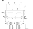
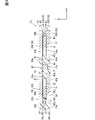
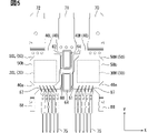
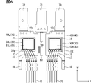
次に、図2~図6に基づき、半導体装置の一例について説明する。図3、図4は、図2のIII-III線、IV-IV線に沿う断面図である。図5は、図2に対して封止樹脂体を省略した図である。図6は、図5に対してエミッタ電極側のヒートシンクを省略した図である。半導体装置を構成する要素の一部について、符号末尾に上アーム6H側を示す「H」を付与し、下アーム6L側を示す「L」を付与している。要素の他の一部について、便宜上、上アーム6Hと下アーム6Lとで共通の符号を付与している。
<Semiconductor device>
Next, an example of a semiconductor device will be described with reference to FIGS. 2 to 6. FIG. 3 and 4 are cross-sectional views taken along lines III-III and IV-IV in FIG. FIG. 5 is a diagram in which a sealing resin body is omitted from FIG. FIG. 6 is a diagram in which the heat sink on the emitter electrode side is omitted from FIG. Some of the elements constituting the semiconductor device are suffixed with "H" indicating the upper arm 6H side and "L" indicating the lower arm 6L side. Other parts of the elements are given common reference numerals for the upper arm 6H and the lower arm 6L for convenience.

以下では、半導体素子の板厚方向をZ方向、Z方向に直交する一方向、具体的には2つの半導体素子の並び方向をX方向と示す。また、Z方向およびX方向の両方向に直交する方向をY方向と示す。特に断わりのない限り、Z方向から平面視した形状、換言すればX方向およびY方向により規定されるXY面に沿う形状を平面形状とする。また、Z方向からの平面視を単に平面視と示す。 Hereinafter, the plate thickness direction of a semiconductor element is referred to as the Z direction, and one direction orthogonal to the Z direction, specifically, the direction in which two semiconductor elements are arranged is referred to as the X direction. A direction orthogonal to both the Z direction and the X direction is indicated as the Y direction. Unless otherwise specified, a planar shape is defined as a planar shape viewed from the Z direction, in other words, a planar shape along the XY plane defined by the X and Y directions. A plan view from the Z direction is simply referred to as a plan view.

図2~図6に示すように、半導体装置10は、封止樹脂体20と、半導体素子30と、ヒートシンク40と、ヒートシンク50およびターミナル55と、継手部60~62と、主端子70~72および信号端子75を備えている。半導体装置10は、上記した一相分の上下アーム回路6を構成する。 As shown in FIGS. 2 to 6, the semiconductor device 10 includes a sealing resin body 20, a semiconductor element 30, a heat sink 40, a heat sink 50 and terminals 55, joint portions 60 to 62, and main terminals 70 to 72. and a signal terminal 75 . The semiconductor device 10 constitutes the upper and lower arm circuits 6 for one phase described above.

封止樹脂体20は、半導体装置10を構成する他の要素の一部を封止している。他の要素の残りの部分は、封止樹脂体20の外に露出している。封止樹脂体20は、たとえばエポキシ系樹脂を材料とする。封止樹脂体20は、たとえばトランスファモールド法により成形されている。図2~図4に示すように、封止樹脂体20は平面略矩形状をなしている。封止樹脂体20は、表面20aと、Z方向において表面20aとは反対の裏面20bを有している。表面20aおよび裏面20bは、たとえば平坦面となっている。 The encapsulating resin body 20 encapsulates a part of other elements constituting the semiconductor device 10 . The rest of the other elements are exposed outside the sealing resin body 20 . The encapsulating resin body 20 is made of, for example, an epoxy resin. The encapsulating resin body 20 is molded by, for example, a transfer molding method. As shown in FIGS. 2 to 4, the sealing resin body 20 has a substantially rectangular planar shape. The sealing resin body 20 has a front surface 20a and a back surface 20b opposite to the front surface 20a in the Z direction. The front surface 20a and the rear surface 20b are, for example, flat surfaces.

半導体素子30は、シリコン(Si)、シリコンよりもバンドギャップが広いワイドバンドギャップ半導体などを材料とする半導体基板に、素子が形成されてなる。ワイドバンドギャップ半導体としては、たとえばシリコンカーバイド(SiC)、窒化ガリウム(GaN)、酸化ガリウム(Ga)、ダイヤモンドがある。半導体素子30は、半導体チップと称されることがある。 The semiconductor element 30 is formed on a semiconductor substrate made of silicon (Si), a wide bandgap semiconductor having a wider bandgap than silicon, or the like. Wide bandgap semiconductors include, for example, silicon carbide (SiC), gallium nitride (GaN), gallium oxide (Ga 2 O 3 ), and diamond. The semiconductor element 30 is sometimes called a semiconductor chip.

素子は、Z方向に主電流が流れるように縦型構造をなしている。縦型素子として、IGBT、MOSFET、ダイオードなどを採用することができる。本実施形態では、縦型素子として、ひとつのアームを構成するIGBT6iおよびFWD6dが形成されている。縦型素子は、RC(Reverse Conducting)-IGBTである。半導体素子30は、図示しないゲート電極を有している。ゲート電極は、たとえばトレンチ構造をなしている。半導体素子30は、自身の板厚方向、すなわちZ方向における両面に、素子の主電極を有している。具体的には、主電極として、表面側にエミッタ電極31を有し、裏面側にコレクタ電極32を有している。エミッタ電極31は、FWD6dのアノード電極を兼ねている。コレクタ電極32は、FWD6dのカソード電極を兼ねている。エミッタ電極31が表面電極に相当し、コレクタ電極32が裏面電極に相当する。 The device has a vertical structure so that the main current flows in the Z direction. IGBTs, MOSFETs, diodes, and the like can be employed as vertical devices. In this embodiment, the IGBT 6i and the FWD 6d forming one arm are formed as vertical elements. The vertical element is RC (Reverse Conducting)-IGBT. The semiconductor element 30 has a gate electrode (not shown). The gate electrode has, for example, a trench structure. The semiconductor element 30 has main electrodes of the element on both sides in the plate thickness direction, that is, in the Z direction. Specifically, as main electrodes, it has an emitter electrode 31 on the front side and a collector electrode 32 on the back side. The emitter electrode 31 also serves as the anode electrode of the FWD 6d. The collector electrode 32 also serves as the cathode electrode of the FWD 6d. The emitter electrode 31 corresponds to the surface electrode, and the collector electrode 32 corresponds to the back electrode.

半導体素子30は、平面略矩形状をなしている。図6に示すように、半導体素子30は、表面においてエミッタ電極31とは異なる位置に形成されたパッド33を有している。エミッタ電極31およびパッド33は、半導体基板の表面の図示しない保護膜からそれぞれ露出している。エミッタ電極31は、半導体素子30の表面の一部分に形成されている。コレクタ電極32は、裏面のほぼ全面に形成されている。平面視において、コレクタ電極32は、エミッタ電極31よりも面積が大きい。 The semiconductor element 30 has a substantially rectangular planar shape. As shown in FIG. 6, the semiconductor element 30 has a pad 33 formed at a different position from the emitter electrode 31 on the surface. Emitter electrode 31 and pad 33 are exposed from a protective film (not shown) on the surface of the semiconductor substrate. Emitter electrode 31 is formed on a portion of the surface of semiconductor element 30 . The collector electrode 32 is formed almost all over the back surface. In plan view, the collector electrode 32 has a larger area than the emitter electrode 31 .

パッド33は、信号用の電極である。パッド33は、エミッタ電極31と電気的に分離されている。パッド33は、Y方向において、エミッタ電極31の形成領域とは反対側の端部に形成されている。パッド33は、ゲート電極用のゲートパッド33gを含む。本実施形態において、半導体素子30は、5つのパッド33を有している。具体的には、上記したゲートパッド33g、エミッタ電極31の電位を検出するケルビンエミッタ用、電流センス用、半導体素子30の温度を検出する温度センサ(感温ダイオード)のアノード電位用、同じくカソード電位用を有している。5つのパッド33は、平面略矩形状の半導体素子30において、Y方向の一端側にまとめて形成されるとともに、X方向に並んで形成されている。 The pads 33 are electrodes for signals. Pad 33 is electrically isolated from emitter electrode 31 . The pad 33 is formed at the end opposite to the region where the emitter electrode 31 is formed in the Y direction. Pads 33 include a gate pad 33g for a gate electrode. In this embodiment, the semiconductor element 30 has five pads 33 . Specifically, the gate pad 33g, the Kelvin emitter for detecting the potential of the emitter electrode 31, the current sensing, the anode potential of the temperature sensor (temperature sensitive diode) for detecting the temperature of the semiconductor element 30, and the cathode potential have a use. The five pads 33 are collectively formed on one end side in the Y direction of the semiconductor element 30 having a substantially rectangular planar shape, and are formed side by side in the X direction.

半導体装置10は、2つの半導体素子30を備えている。具体的には、上アーム6Hを構成する半導体素子30Hと、下アーム6Lを構成する半導体素子30Lを備えている。半導体素子30H、30Lは、互いに同様の構成を有している。半導体素子30H、30Lは、X方向に並んでいる。半導体素子30H、30Lは、Z方向において互いにほぼ同じ位置に配置されている。 The semiconductor device 10 has two semiconductor elements 30 . Specifically, it includes a semiconductor element 30H forming the upper arm 6H and a semiconductor element 30L forming the lower arm 6L. The semiconductor elements 30H and 30L have mutually similar configurations. The semiconductor elements 30H and 30L are arranged in the X direction. The semiconductor elements 30H and 30L are arranged at substantially the same positions in the Z direction.

ヒートシンク40は、Z方向において半導体素子30の裏面側に配置され、はんだ80を介して、コレクタ電極32と電気的に接続された配線部材である。はんだ80は、ヒートシンク40とコレクタ電極32とを接続(接合)している。ヒートシンク40が裏側配線部材に相当し、はんだ80が裏側接合部材に相当する。ヒートシンク40は、半導体素子30との対向面である実装面40aと、実装面40aとは反対の面である裏面40bを有している。ヒートシンク40の実装面40aと半導体素子30のコレクタ電極32との間にはんだ80が介在し、はんだ接合部が形成されている。 The heat sink 40 is a wiring member arranged on the back side of the semiconductor element 30 in the Z direction and electrically connected to the collector electrode 32 via solder 80 . The solder 80 connects (joins) the heat sink 40 and the collector electrode 32 . The heat sink 40 corresponds to the back wiring member, and the solder 80 corresponds to the back bonding member. The heat sink 40 has a mounting surface 40a facing the semiconductor element 30 and a back surface 40b opposite to the mounting surface 40a. Solder 80 is interposed between the mounting surface 40a of the heat sink 40 and the collector electrode 32 of the semiconductor element 30 to form a solder joint.

ヒートシンク40は、半導体素子30の熱を外部に放熱する。ヒートシンク40としては、たとえばCu、Cu合金などを材料とする金属板、DBC(Direct Bonded Copper)基板などを採用することができる。表面に、NiやAuなどのめっき膜を備えてもよい。本実施形態において、ヒートシンク40は、Cuを材料とする金属板である。ヒートシンク40は、放熱部材、導電部材、リードフレームと称されることがある。半導体装置10は、2つのヒートシンク40を備えている。具体的には、上アーム6Hを構成するヒートシンク40Hと、下アーム6Lを構成するヒートシンク40Lを備えている。 The heat sink 40 radiates the heat of the semiconductor element 30 to the outside. As the heat sink 40, for example, a metal plate made of Cu, a Cu alloy, or the like, a DBC (Direct Bonded Copper) substrate, or the like can be used. A plated film of Ni, Au, or the like may be provided on the surface. In this embodiment, the heat sink 40 is a metal plate made of Cu. The heat sink 40 may be called a heat dissipation member, a conductive member, or a lead frame. The semiconductor device 10 has two heat sinks 40 . Specifically, a heat sink 40H forming the upper arm 6H and a heat sink 40L forming the lower arm 6L are provided.

図6に示すように、ヒートシンク40H、40Lは、平面略矩形状をなしている。ヒートシンク40H、40Lは、X方向に並んでいる。図3および図4に示すように、ヒートシンク40H、40Lは、互いにほぼ同じ厚みを有し、Z方向において互いにほぼ同じ位置に配置されている。ヒートシンク40Hの実装面40aと半導体素子30Hのコレクタ電極32との間、および、ヒートシンク40Lの実装面40aと半導体素子30Lのコレクタ電極32との間のそれぞれに、はんだ接合部が形成されている。 As shown in FIG. 6, the heat sinks 40H and 40L are substantially rectangular in plan view. The heat sinks 40H and 40L are arranged in the X direction. As shown in FIGS. 3 and 4, the heat sinks 40H and 40L have approximately the same thickness and are arranged at approximately the same position in the Z direction. Solder joints are formed between the mounting surface 40a of the heat sink 40H and the collector electrode 32 of the semiconductor element 30H and between the mounting surface 40a of the heat sink 40L and the collector electrode 32 of the semiconductor element 30L.

ヒートシンク40H、40Lは、Z方向からの平面視において、対応する半導体素子30を内包している。ヒートシンク40H、40Lの裏面40bは、封止樹脂体20から露出している。裏面40bは、放熱面、露出面と称されることがある。裏面40bは、封止樹脂体20の裏面20bと略面一である。ヒートシンク40H、40Lの裏面40bは、X方向に並んでいる。 The heat sinks 40H and 40L enclose the corresponding semiconductor elements 30 in plan view from the Z direction. The back surfaces 40b of the heat sinks 40H and 40L are exposed from the sealing resin body 20. As shown in FIG. The back surface 40b is sometimes called a heat dissipation surface or an exposed surface. The back surface 40 b is substantially flush with the back surface 20 b of the sealing resin body 20 . The back surfaces 40b of the heat sinks 40H and 40L are arranged in the X direction.

ヒートシンク50およびターミナル55は、Z方向において半導体素子30の表面側に配置され、はんだ81、82を介して、エミッタ電極31と電気的に接続された配線部材である。ターミナル55は、Z方向において半導体素子30とヒートシンク50との間に介在している。はんだ81は、ターミナル55とエミッタ電極31とを接続(接合)している。はんだ82は、ヒートシンク50とターミナル55とを接続(接合)している。 The heat sink 50 and the terminal 55 are wiring members arranged on the surface side of the semiconductor element 30 in the Z direction and electrically connected to the emitter electrode 31 via solders 81 and 82 . Terminal 55 is interposed between semiconductor element 30 and heat sink 50 in the Z direction. The solder 81 connects (joins) the terminal 55 and the emitter electrode 31 . The solder 82 connects (joins) the heat sink 50 and the terminal 55 .

ターミナル55は、半導体素子30との対向面である第1端面55aと、第1端面55aとは反対の面である第2端面55bを有している。ヒートシンク50は、第2端面55bとの対向面である実装面50aと、実装面50aとは反対の面である裏面50bを有している。実装面50aは、ヒートシンク50において半導体素子30側の面である。ターミナル55の第1端面55aと半導体素子30のエミッタ電極31との間にはんだ81が介在し、はんだ接合部が形成されている。ターミナル55の第2端面55bとヒートシンク50の実装面50aとの間にはんだ82が介在し、はんだ接合部が形成されている。ヒートシンク50およびターミナル55が、表側配線部材に相当する。はんだ81が、表側接合部材に相当する。 The terminal 55 has a first end surface 55a facing the semiconductor element 30 and a second end surface 55b opposite to the first end surface 55a. The heat sink 50 has a mounting surface 50a facing the second end surface 55b and a back surface 50b opposite to the mounting surface 50a. The mounting surface 50 a is the surface of the heat sink 50 on the semiconductor element 30 side. Solder 81 is interposed between the first end surface 55a of the terminal 55 and the emitter electrode 31 of the semiconductor element 30 to form a solder joint. Solder 82 is interposed between the second end surface 55b of the terminal 55 and the mounting surface 50a of the heat sink 50 to form a solder joint. The heat sink 50 and the terminals 55 correspond to front side wiring members. The solder 81 corresponds to the front joint member.

ターミナル55は、半導体素子30(エミッタ電極31)とヒートシンク50との電気伝導、熱伝導経路の途中に位置する。ターミナル55は、Cu、Cu合金などの金属材料を含んでいる。表面に、めっき膜を備えてもよい。ターミナル55H、55Lは、平面視においてエミッタ電極31とほぼ同じ大きさを有する平面略矩形状の柱状体である。ターミナル55は、金属ブロック体、中継部材と称されることがある。半導体装置10は、2つのターミナル55を備えている。具体的には、上アーム6Hを構成するターミナル55Hと、下アーム6Lを構成するターミナル55Lを備えている。ターミナル55Hの第1端面55aと半導体素子30Hのエミッタ電極31との間、および、ターミナル55Lの第1端面55aと半導体素子30Lのエミッタ電極31との間に、はんだ接合部がそれぞれ形成されている。 The terminal 55 is located in the middle of the electrical and thermal conduction paths between the semiconductor element 30 (emitter electrode 31 ) and the heat sink 50 . The terminal 55 contains a metallic material such as Cu or Cu alloy. A plating film may be provided on the surface. The terminals 55H and 55L are substantially rectangular columnar bodies having substantially the same size as the emitter electrode 31 in plan view. The terminal 55 is sometimes called a metal block or relay member. The semiconductor device 10 has two terminals 55 . Specifically, a terminal 55H forming the upper arm 6H and a terminal 55L forming the lower arm 6L are provided. Solder joints are formed between the first end surface 55a of the terminal 55H and the emitter electrode 31 of the semiconductor element 30H and between the first end surface 55a of the terminal 55L and the emitter electrode 31 of the semiconductor element 30L. .

ヒートシンク50は、半導体素子30の熱を外部に放熱する。ヒートシンク50は、ヒートシンク40と同様の構成を有している。本実施形態において、ヒートシンク50は、Cuを材料とする金属板である。半導体装置10は、2つのヒートシンク50を備えている。具体的には、上アーム6Hを構成するヒートシンク50Hと、下アーム6Lを構成するヒートシンク50Lを備えている。 The heat sink 50 radiates the heat of the semiconductor element 30 to the outside. The heat sink 50 has a configuration similar to that of the heat sink 40 . In this embodiment, the heat sink 50 is a metal plate made of Cu. The semiconductor device 10 has two heat sinks 50 . Specifically, a heat sink 50H forming the upper arm 6H and a heat sink 50L forming the lower arm 6L are provided.

図5に示すように、ヒートシンク50H、50Lは、平面略矩形状をなしている。ヒートシンク50H、50Lは、X方向に並んでいる。図3および図4に示すように、ヒートシンク50H、50Lは、互いにほぼ同じ厚みを有し、Z方向において互いにほぼ同じ位置に配置されている。ヒートシンク50Hの実装面50aとターミナル55Hの第2端面55bとの間、および、ヒートシンク50Lの実装面50aとターミナル55Lの第2端面55bとの間のそれぞれに、はんだ接合部が形成されている。 As shown in FIG. 5, the heat sinks 50H and 50L are substantially rectangular in plan view. The heat sinks 50H and 50L are arranged in the X direction. As shown in FIGS. 3 and 4, the heat sinks 50H and 50L have approximately the same thickness and are arranged at approximately the same position in the Z direction. Solder joints are formed between the mounting surface 50a of the heat sink 50H and the second end surfaces 55b of the terminals 55H and between the mounting surface 50a of the heat sink 50L and the second end surfaces 55b of the terminals 55L.

ヒートシンク50H、50Lは、Z方向からの平面視において、対応する半導体素子30およびターミナル55を内包している。ヒートシンク50H、50Lの実装面50aには、溢れたはんだ82を収容する溝51が形成されている。溝51は、実装面50aにおいてはんだ接合部を取り囲んでいる。溝51は、たとえば環状に形成されている。ヒートシンク50H、50Lの裏面50bは、封止樹脂体20から露出している。裏面50bは、放熱面、露出面と称されることがある。裏面50bは、封止樹脂体20の表面20aと略面一である。ヒートシンク50H、50Lの裏面50bは、X方向に並んでいる。 The heat sinks 50H and 50L enclose the corresponding semiconductor elements 30 and terminals 55 in plan view from the Z direction. A groove 51 is formed in the mounting surface 50a of the heat sinks 50H and 50L to accommodate the overflowing solder 82. As shown in FIG. The groove 51 surrounds the solder joint on the mounting surface 50a. Groove 51 is formed, for example, in an annular shape. The back surfaces 50b of the heat sinks 50H and 50L are exposed from the sealing resin body 20. As shown in FIG. The back surface 50b is sometimes called a heat dissipation surface or an exposed surface. The back surface 50b is substantially flush with the front surface 20a of the sealing resin body 20. As shown in FIG. The back surfaces 50b of the heat sinks 50H and 50L are arranged in the X direction.

継手部60~62は、上下アーム回路6を構成する要素間をつないでいる。継手部は、半導体装置10を構成する要素間をつないでいる。図3および図6に示すように、継手部60は、ヒートシンク40Lに連なっている。継手部60の厚みは、ヒートシンク40Lよりも薄い。継手部60は、ヒートシンク40Lの実装面40aと略面一の状態で、ヒートシンク40Hとの対向面(側面)に連なっている。継手部60は、2つの屈曲部を有することで、ZX平面において略クランク状をなしている。継手部60は、封止樹脂体20によって覆われている。継手部60は、ヒートシンク40Lに対して一体的に設けられることで連なってもよいし、別部材として設けられ、接続により連なってもよい。本実施形態において、継手部60は、リードフレームの一部として、ヒートシンク40Lと一体的に設けられている。 The joints 60 to 62 connect the elements forming the upper and lower arm circuits 6 . The joint section connects elements constituting the semiconductor device 10 . As shown in FIGS. 3 and 6, the joint portion 60 continues to the heat sink 40L. The joint portion 60 is thinner than the heat sink 40L. The joint portion 60 is connected to a surface (side surface) facing the heat sink 40H while being substantially flush with the mounting surface 40a of the heat sink 40L. The joint portion 60 has a substantially crank shape in the ZX plane by having two bent portions. The joint portion 60 is covered with the sealing resin body 20 . The joint part 60 may be connected to the heat sink 40L by being provided integrally with the heat sink 40L, or may be provided as a separate member and connected to the heat sink 40L. In this embodiment, the joint portion 60 is provided integrally with the heat sink 40L as part of the lead frame.

図3および図5に示すように、継手部61、62は、対応するヒートシンク50に連なっている。継手部61は、ヒートシンク50Hに連なっている。継手部62は、ヒートシンク50Lに連なっている。継手部61、62の厚みは、対応するヒートシンク50よりも薄い。継手部61、62は、封止樹脂体20によって覆われている。継手部61、62は、ヒートシンク50に対して一体的に設けられることで連なってもよいし、別部材として設けられ、接続により連なってもよい。本実施形態において、継手部61、62は、対応するヒートシンク50H、50Lに対して一体的に設けられている。継手部61、62は、2つのヒートシンク50H、50Lにおいて、互いに対向する側面からX方向に延設されている。 As shown in FIGS. 3 and 5 , the joints 61 and 62 are connected to the corresponding heat sinks 50 . The joint portion 61 continues to the heat sink 50H. The joint portion 62 continues to the heat sink 50L. The joint portions 61 , 62 are thinner than the corresponding heat sink 50 . The joint portions 61 and 62 are covered with the sealing resin body 20 . The joint portions 61 and 62 may be connected by being provided integrally with the heat sink 50, or may be provided as separate members and connected by connection. In this embodiment, the joint portions 61 and 62 are provided integrally with the corresponding heat sinks 50H and 50L. The joint portions 61 and 62 extend in the X direction from the side surfaces facing each other in the two heat sinks 50H and 50L.

継手部61を含むヒートシンク50Hと、継手部62を含むヒートシンク50Lとが共通部材となっている。継手部61を含むヒートシンク50Hと、継手部62を含むヒートシンク50Lとの配置は、Z軸を回転軸とする2回対称となっている。継手部60と継手部61との対向面間にはんだ83が介在し、はんだ接合部が形成されている。 The heat sink 50H including the joint portion 61 and the heat sink 50L including the joint portion 62 are common members. The arrangement of the heat sink 50H including the joint portion 61 and the heat sink 50L including the joint portion 62 is two-fold symmetrical about the Z-axis as the rotation axis. Solder 83 is interposed between the facing surfaces of joint portion 60 and joint portion 61 to form a solder joint.

継手部61の接合面には、溢れたはんだ83を収容する溝63が形成されている。溝63は、はんだ接合部を取り囲むように環状に形成されている。同様に、継手部62の接合面にも、溢れたはんだを収容する溝63が形成されている。本実施形態において、溝63がプレス加工により形成されている。このため、継手部61、62は、溝63の裏面側に凸部64を有している。 A groove 63 is formed in the joint surface of the joint portion 61 to accommodate the overflowing solder 83 . The groove 63 is annularly formed so as to surround the solder joint. Similarly, grooves 63 are also formed on the joint surface of the joint portion 62 to accommodate overflowing solder. In this embodiment, the grooves 63 are formed by pressing. For this reason, the joint portions 61 and 62 have a convex portion 64 on the back side of the groove 63 .

主端子70~72および信号端子75は、外部接続端子である。主端子70、71は、電源端子である。主端子70は、平滑コンデンサ4の正極端子と電気的に接続される。主端子71は、平滑コンデンサ4の負極端子と電気的に接続される。このため、主端子70はP端子、主端子71はN端子と称されることがある。 The main terminals 70 to 72 and the signal terminal 75 are external connection terminals. The main terminals 70 and 71 are power supply terminals. Main terminal 70 is electrically connected to the positive terminal of smoothing capacitor 4 . Main terminal 71 is electrically connected to the negative terminal of smoothing capacitor 4 . Therefore, the main terminal 70 is sometimes called the P terminal, and the main terminal 71 is sometimes called the N terminal.

図5および図6に示すように、主端子70は、ヒートシンク40HにおけるY方向の一端に連なっている。主端子70の厚みは、ヒートシンク40Hよりも薄い。主端子70は、実装面40aと略面一でヒートシンク40Hに連なっている。主端子70は、ヒートシンク40HからY方向に延設され、封止樹脂体20の側面20cから外部に突出している。主端子70は、封止樹脂体20により覆われる部分の途中に屈曲部を有し、側面20cにおいてZ方向の中央付近から突出している。 As shown in FIGS. 5 and 6, the main terminal 70 continues to one end of the heat sink 40H in the Y direction. The thickness of the main terminal 70 is thinner than the heat sink 40H. The main terminal 70 is substantially flush with the mounting surface 40a and continues to the heat sink 40H. The main terminal 70 extends in the Y direction from the heat sink 40H and protrudes from the side surface 20c of the sealing resin body 20 to the outside. The main terminal 70 has a bent portion in the middle of the portion covered with the sealing resin body 20, and protrudes from the vicinity of the center in the Z direction on the side surface 20c.

図4および図5に示すように、主端子71は、継手部62に接続されている。主端子71と継手部62との対向面間にはんだ84が介在し、はんだ接合部が形成されている。主端子71は、Y方向に延設されて、主端子70と同じ側面20cから封止樹脂体20の外に突出している。主端子71は、Y方向の一端付近に継手部62との接続部71aを有している。主端子71のうち、接続部71aを含む一部分が封止樹脂体20により覆われ、残りの部分が封止樹脂体20から突出している。接続部71aは、封止樹脂体20から突出した部分よりも板厚が厚い。接続部71aの板厚は、たとえばヒートシンク40とほぼ同じ厚みである。主端子71も、主端子同様に屈曲部を有し、側面20cにおいてZ方向の中央付近から突出している。 As shown in FIGS. 4 and 5, the main terminal 71 is connected to the joint portion 62 . Solder 84 is interposed between the facing surfaces of the main terminal 71 and the joint portion 62 to form a solder joint. The main terminal 71 extends in the Y direction and protrudes outside the sealing resin body 20 from the same side surface 20 c as the main terminal 70 . The main terminal 71 has a connecting portion 71a connected to the joint portion 62 near one end in the Y direction. A portion of the main terminal 71 including the connection portion 71 a is covered with the sealing resin body 20 , and the remaining portion protrudes from the sealing resin body 20 . The connecting portion 71 a is thicker than the portion protruding from the sealing resin body 20 . The plate thickness of the connecting portion 71a is substantially the same as that of the heat sink 40, for example. The main terminal 71 also has a bent portion similarly to the main terminal, and protrudes from the vicinity of the center in the Z direction on the side surface 20c.

主端子72は、上アーム6Hと下アーム6Lとの接続点に接続されている。主端子72は、モータジェネレータ3の対応する相の巻線(固定子コイル)と電気的に接続される。主端子72は、出力端子、交流端子、O端子とも称される。主端子72は、ヒートシンク40LにおけるY方向の一端に連なっている。主端子72の厚みは、ヒートシンク40Lよりも薄い。主端子72は、実装面40aと略面一でヒートシンク40Lに連なっている。主端子72は、ヒートシンク40LからY方向に延設され、主端子70と同じ側面20cから封止樹脂体20の外に突出している。主端子72も、主端子71同様に屈曲部を有し、側面20cにおいてZ方向の中央付近から突出している。3本の主端子70~72は、X方向において主端子70、主端子71、主端子72の順に配置されている。 The main terminal 72 is connected to a connection point between the upper arm 6H and the lower arm 6L. Main terminal 72 is electrically connected to a corresponding phase winding (stator coil) of motor generator 3 . The main terminal 72 is also called an output terminal, an AC terminal, or an O terminal. The main terminal 72 continues to one end of the heat sink 40L in the Y direction. The thickness of the main terminals 72 is thinner than the heat sink 40L. The main terminal 72 is substantially flush with the mounting surface 40a and continues to the heat sink 40L. The main terminals 72 extend from the heat sink 40</b>L in the Y direction and protrude out of the sealing resin body 20 from the same side surface 20 c as the main terminals 70 . Like the main terminal 71, the main terminal 72 also has a bent portion and protrudes from the vicinity of the center in the Z direction on the side surface 20c. The three main terminals 70 to 72 are arranged in the order of main terminal 70, main terminal 71, and main terminal 72 in the X direction.

信号端子75は、対応する半導体素子30のパッド33に電気的に接続されている。本実施形態では、ボンディングワイヤ87を介して電気的に接続されている。信号端子75は、Y方向に延設されており、封止樹脂体20の側面20dから外部に突出している。側面20dは、Y方向において側面20cとは反対の面である。本実施形態では、ひとつの半導体素子30に対して5本の信号端子75が設けられている。 The signal terminals 75 are electrically connected to the pads 33 of the corresponding semiconductor element 30 . In this embodiment, they are electrically connected via bonding wires 87 . The signal terminal 75 extends in the Y direction and protrudes from the side surface 20d of the sealing resin body 20 to the outside. The side surface 20d is a surface opposite to the side surface 20c in the Y direction. In this embodiment, five signal terminals 75 are provided for one semiconductor element 30 .

なお、図2、図5、および図6に示す符号88は、吊りリードである。ヒートシンク40(40H、40L)と、継手部60と、主端子70~72と、信号端子75は、共通部材であるリードフレームに構成されている。このリードフレームは部分的に厚みが異なる異形条である。信号端子75は、カット前の状態で、タイバーを介して吊りリード88に接続される。タイバーなど、リードフレームの不要部分は、封止樹脂体20の成形後にカット(除去)されている。 Reference numeral 88 shown in FIGS. 2, 5, and 6 is a suspension lead. The heat sink 40 (40H, 40L), the joint portion 60, the main terminals 70 to 72, and the signal terminal 75 are configured in a lead frame as a common member. This lead frame is a multi-gauge strip with partially different thicknesses. The signal terminal 75 is connected to the suspension lead 88 through a tie bar before being cut. Unnecessary portions of the lead frame such as tie bars are cut (removed) after the sealing resin body 20 is molded.

上記したように、半導体装置10では、封止樹脂体20によって一相分の上下アーム回路6を構成する複数の半導体素子30が封止されている。封止樹脂体20は、複数の半導体素子30、ヒートシンク40それぞれの一部、ヒートシンク50それぞれの一部、ターミナル55、継手部60~62、主端子70~72および信号端子75それぞれの一部を、一体的に封止している。 As described above, in the semiconductor device 10 , the plurality of semiconductor elements 30 forming the upper and lower arm circuits 6 for one phase are sealed with the sealing resin body 20 . The sealing resin body 20 partially covers the semiconductor elements 30, the heat sinks 40, the heat sinks 50, the terminals 55, the joints 60 to 62, the main terminals 70 to 72, and the signal terminals 75. , integrally sealed.

Z方向において、ヒートシンク40、50の間に、半導体素子30が配置されている。これにより、半導体素子30の熱を、Z方向において両側に放熱することができる。半導体装置10は、両面放熱構造をなしている。ヒートシンク40の裏面40bは、封止樹脂体20の裏面20bと略面一となっている。ヒートシンク50の裏面50bは、封止樹脂体20の表面20aと略面一となっている。裏面40b、50bが露出面であるため、放熱性を高めることができる。 A semiconductor element 30 is arranged between the heat sinks 40 and 50 in the Z direction. Thereby, the heat of the semiconductor element 30 can be dissipated to both sides in the Z direction. The semiconductor device 10 has a double-sided heat dissipation structure. The back surface 40 b of the heat sink 40 is substantially flush with the back surface 20 b of the sealing resin body 20 . The back surface 50 b of the heat sink 50 is substantially flush with the front surface 20 a of the sealing resin body 20 . Since the back surfaces 40b and 50b are exposed surfaces, heat dissipation can be enhanced.

<ワイヤ片>
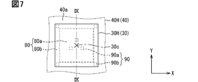
次に、図7~図9に基づき、ワイヤ片について説明する。図7は、図6において上アーム6H側の半導体素子30H周辺を拡大した平面図である。図7は、半導体素子とワイヤ片との位置関係を示している。図7では、便宜上、ターミナル55H、はんだ81、エミッタ電極31、パッド33、およびボンディングワイヤ87を省略して図示している。図8は、ワイヤ片の配置を示す斜視図である。図9は、図7のIX-IX線に沿う断面図である。
<Wire piece>
Next, the wire piece will be described with reference to FIGS. 7 to 9. FIG. FIG. 7 is an enlarged plan view of the periphery of the semiconductor element 30H on the upper arm 6H side in FIG. FIG. 7 shows the positional relationship between the semiconductor element and the wire piece. In FIG. 7, the terminal 55H, the solder 81, the emitter electrode 31, the pad 33, and the bonding wire 87 are omitted for convenience. FIG. 8 is a perspective view showing the arrangement of wire pieces. 9 is a cross-sectional view taken along line IX-IX in FIG. 7. FIG.

図7~図9に示すように、半導体装置10は、ワイヤ片90をさらに備えている。ワイヤ片90は、主電極と配線部材とを電気的に接続するはんだ接合部の少なくともひとつに設けられている。ワイヤ片90は、はんだ内に配置されている。ひとつ(単一)のはんだに対して、複数のワイヤ片90が分散配置されている。複数のワイヤ片90は、はんだ接合部を構成する対向面のひとつである第1対向面に固定(接合)され、対向面の他のひとつである第2対向面に向けて突起している。 As shown in FIGS. 7-9, the semiconductor device 10 further includes a wire piece 90. FIG. A wire piece 90 is provided in at least one of the solder joints that electrically connect the main electrode and the wiring member. A piece of wire 90 is placed in the solder. A plurality of wire pieces 90 are distributed for one (single) solder. The plurality of wire pieces 90 are fixed (joined) to a first opposing surface, which is one of the opposing surfaces that form the solder joint, and protrude toward a second opposing surface, which is the other one of the opposing surfaces.

ワイヤ片90は、はんだの最低膜厚を確保すべく、所定高さを有している。複数のワイヤ片90が第2対向面に接触した状態においても、第1対向面と第2対向面との最短距離が最低膜厚以上となるように、ワイヤ片90の高さが設定されている。最低膜厚とは、所望の接続信頼性を確保するために必要な最低限の厚みである。ワイヤ片90の高さは、たとえば最低膜厚にマージンを加味した値である。ワイヤ片90は、ボンディングワイヤの小片部である。ワイヤ片90は、突起部、スタッドボンディングと称されることがある。 The wire piece 90 has a predetermined height in order to ensure the minimum film thickness of the solder. The height of the wire pieces 90 is set so that the shortest distance between the first opposing surface and the second opposing surface is equal to or greater than the minimum film thickness even when the plurality of wire pieces 90 are in contact with the second opposing surface. there is The minimum film thickness is the minimum thickness required to ensure desired connection reliability. The height of the wire piece 90 is, for example, a value obtained by adding a margin to the minimum film thickness. Wire piece 90 is a small piece of bonding wire. Wire pieces 90 are sometimes referred to as protrusions or stud bonds.

本実施形態では、複数のワイヤ片90が、半導体素子30Hのコレクタ電極32とヒートシンク40Hの実装面40aとの間のはんだ80に配置されている。複数のワイヤ片90は、そのすべてがヒートシンク40Hの実装面40aに固定(接合)されており、半導体素子30Hの裏面、すなわちコレクタ電極32上には固定されていない。ヒートシンク40Hの実装面40aが第1対向面に相当し、半導体素子30Hの裏面が第2対向面に相当する。実装面40aには、複数のワイヤ片90が固定されている。ワイヤ片90は、アルミニウムやアルミニウム合金を材料とするボンディングワイヤの小片部である。実装面40aに固定されたすべてのワイヤ片90が、はんだ80内に配置されている。 In this embodiment, a plurality of wire pieces 90 are arranged in the solder 80 between the collector electrode 32 of the semiconductor element 30H and the mounting surface 40a of the heat sink 40H. All of the plurality of wire pieces 90 are fixed (bonded) to the mounting surface 40a of the heat sink 40H, and are not fixed to the back surface of the semiconductor element 30H, that is, the collector electrode 32. FIG. The mounting surface 40a of the heat sink 40H corresponds to the first facing surface, and the back surface of the semiconductor element 30H corresponds to the second facing surface. A plurality of wire pieces 90 are fixed to the mounting surface 40a. The wire piece 90 is a small piece of bonding wire made of aluminum or an aluminum alloy. All the wire pieces 90 fixed to the mounting surface 40a are arranged in the solder 80. FIG.

はんだ80は、平面視において、半導体素子30Hの中央部分と重なる中央領域80aと、中央領域80aを取り囲む外周領域80bを有している。半導体素子30Hの中央部分は、素子中心30cとその周囲部分である。半導体素子30Hは、中央部分を取り囲む外周部分を有している。外周部分は、たとえば平面矩形状の4辺のそれぞれから所定範囲の部分である。たとえば中央部分は素子が形成されたアクティブ領域であり、外周部分はアクティブ領域を取り囲む外周耐圧領域である。外周領域80bは、半導体素子30Hの外周部分と重なる部分を含んでいる。中央領域80aおよび外周領域80bのそれぞれに、複数のワイヤ片90が配置されている。 The solder 80 has a central region 80a overlapping the central portion of the semiconductor element 30H and an outer peripheral region 80b surrounding the central region 80a in plan view. The central portion of the semiconductor element 30H is the element center 30c and its peripheral portion. The semiconductor element 30H has an outer peripheral portion surrounding the central portion. The outer peripheral portion is, for example, a portion within a predetermined range from each of the four sides of the flat rectangular shape. For example, the central portion is an active region in which elements are formed, and the peripheral portion is a peripheral breakdown voltage region surrounding the active region. The peripheral region 80b includes a portion that overlaps the peripheral portion of the semiconductor element 30H. A plurality of wire pieces 90 are arranged in each of the central region 80a and the outer peripheral region 80b.

実装面40aに固定されたワイヤ片90の一部である複数のワイヤ片90aは、平面視において素子中心30cを取り囲むように、中央領域80aに配置されている。図7に示す中心線CLは、素子中心30cを通り、Z方向に延びる仮想線である。中央領域80aのワイヤ片90aは、この中心線CLを取り囲んでいる。素子中心30cを取り囲むために、中央領域80aには3つ以上のワイヤ片90aが配置されている。本実施形態では、中央領域80aに3つのワイヤ片90aが配置されている。3つのワイヤ片90aは、素子中心30cに対して3回対称の位置関係となっている。 A plurality of wire pieces 90a, which are part of the wire pieces 90 fixed to the mounting surface 40a, are arranged in the central region 80a so as to surround the element center 30c in plan view. A center line CL shown in FIG. 7 is a virtual line passing through the element center 30c and extending in the Z direction. The wire piece 90a of the central region 80a surrounds this centerline CL. Three or more wire strips 90a are arranged in the central region 80a to surround the element center 30c. In this embodiment, three wire pieces 90a are arranged in the central region 80a. The three wire pieces 90a have a positional relationship of three-fold symmetry with respect to the element center 30c.

実装面40aに固定されたワイヤ片90の他の一部である複数のワイヤ片90bは、平面視において素子中心30cを取り囲むように、外周領域80bに配置されている。複数のワイヤ片90bは、少なくとも平面矩形状をなす半導体素子30Hの四隅のそれぞれに対応して配置されている。このため、外周領域80bには、4つ以上のワイヤ片90bが配置されている。本実施形態では、外周領域80bに4つのワイヤ片90bが配置されている。ワイヤ片90bは、半導体素子30Hの四隅と重なる部分に配置されている。なお、四隅とは、平面矩形状の4つの角(頂点)を指すのではなく、頂点を含む所定範囲の部分(角周辺の部分)である。 A plurality of wire pieces 90b, which are other parts of the wire piece 90 fixed to the mounting surface 40a, are arranged in the outer peripheral region 80b so as to surround the element center 30c in plan view. The plurality of wire pieces 90b are arranged corresponding to each of the four corners of at least the planar rectangular semiconductor element 30H. Therefore, four or more wire pieces 90b are arranged in the outer peripheral region 80b. In this embodiment, four wire pieces 90b are arranged in the outer peripheral region 80b. The wire pieces 90b are arranged at portions overlapping the four corners of the semiconductor element 30H. Note that the four corners do not refer to four corners (vertices) of a flat rectangular shape, but to portions within a predetermined range (portions around the corners) including the vertices.

なお、下アーム6L側も同様の構成を有している。すなわち、半導体素子30Lのコレクタ電極32とヒートシンク40Lの実装面40aとの間のはんだ80に、複数のワイヤ片90が配置されている。複数のワイヤ片90は、実装面40aに固定されている。このため、説明を省略する。 The lower arm 6L side also has a similar configuration. That is, a plurality of wire pieces 90 are arranged on the solder 80 between the collector electrode 32 of the semiconductor element 30L and the mounting surface 40a of the heat sink 40L. A plurality of wire pieces 90 are fixed to the mounting surface 40a. Therefore, the description is omitted.

<半導体装置の製造方法>
次に、上記した半導体装置10の製造方法について説明する。本実施形態では、ソルダダイボンド法を用いて、半導体装置10を形成する。
<Method for manufacturing a semiconductor device>
Next, a method for manufacturing the semiconductor device 10 described above will be described. In this embodiment, the semiconductor device 10 is formed using the solder die bonding method.

先ず、ワイヤ片90を形成する。リードフレームにおけるヒートシンク40の実装面40aに、アルミニウム系のボンディングワイヤを超音波接合する。ボンディングワイヤは通常、2つの部分を電気的に接続すべく、1stボンド部と2ndボンド部を有する。ここでは、1stボンド部を形成した時点でワイヤをカットし、ワイヤ片90とする。 First, a piece of wire 90 is formed. An aluminum-based bonding wire is ultrasonically bonded to the mounting surface 40a of the heat sink 40 in the lead frame. A bonding wire usually has a 1st bond portion and a 2nd bond portion to electrically connect the two portions. Here, the wire is cut to form a wire piece 90 when the 1st bond portion is formed.

次いで、溶融はんだを塗布して積層体を形成する。先ず、実装面40a上に溶融はんだ(はんだ80)を塗布し、コレクタ電極32が実装面40a側となるように、溶融はんだ上に半導体素子30を配置する。次いで、半導体素子30のエミッタ電極31上に溶融はんだ(はんだ81)を塗布し、第1端面55aが半導体素子30側となるように、溶融はんだ上にターミナル55を配置する。さらにターミナル55の第2端面55b上に溶融はんだ(はんだ82)を塗布する。また、継手部60および接続部71a上にも溶融はんだ(はんだ83、84)を塗布する。溶融はんだは、たとえば転写法を用いて塗布することができる。塗布した溶融はんだが固化(凝固)することで、ヒートシンク40、半導体素子30、およびターミナル55の積層体が得られる。 Molten solder is then applied to form a laminate. First, molten solder (solder 80) is applied onto the mounting surface 40a, and the semiconductor element 30 is placed on the molten solder so that the collector electrode 32 faces the mounting surface 40a. Next, molten solder (solder 81) is applied onto the emitter electrode 31 of the semiconductor element 30, and the terminal 55 is arranged on the molten solder so that the first end face 55a faces the semiconductor element 30 side. Further, molten solder (solder 82) is applied onto the second end face 55b of the terminal 55. Then, as shown in FIG. Molten solder (solders 83 and 84) is also applied onto the joint portion 60 and the connection portion 71a. Molten solder can be applied, for example, using a transfer method. By solidifying (solidifying) the applied molten solder, a laminate of the heat sink 40, the semiconductor element 30, and the terminals 55 is obtained.

すべてのはんだ80~84を一括で固化(凝固)させてもよいし、積層順に固化(凝固)させてもよい。一括で行うことで、製造工程を簡素化(たとえば製造時間を短縮)することができる。ボンディングワイヤ87の接続は、積層体の状態で行ってもよいし、はんだ80が固化した状態で、はんだ81を塗布する前に行ってもよい。すべてのはんだ80~84の塗布が完了した積層体の状態でのボンディングのほうが、塗布装置の接触等による不良を抑制できるため好ましい。 All the solders 80 to 84 may be solidified (solidified) at once, or may be solidified (solidified) in the order of lamination. By carrying out collectively, the manufacturing process can be simplified (for example, the manufacturing time can be shortened). The connection of the bonding wire 87 may be performed in the state of the laminate, or may be performed in the state of the solidified solder 80 before the solder 81 is applied. Bonding in the state of the laminated body in which all the solders 80 to 84 have been applied is preferable because it is possible to suppress defects due to contact with the application device.

両面放熱構造の半導体装置10は、たとえば図示しない冷却器によってZ方向の両面側から挟まれる。よって、Z方向において表面の高い平行度と表面間の高い寸法精度が求められる。このため、はんだ82については、半導体装置10の高さばらつきを吸収可能な量を配置する。すなわち、多めのはんだ82を配置する。たとえば、はんだ82は、はんだ80、81よりも厚くなる。 A semiconductor device 10 having a double-sided heat dissipation structure is sandwiched from both sides in the Z direction by coolers (not shown), for example. Therefore, high parallelism of the surfaces in the Z direction and high dimensional accuracy between the surfaces are required. For this reason, the solder 82 is arranged in an amount capable of absorbing the height variation of the semiconductor device 10 . That is, a large amount of solder 82 is arranged. For example, solder 82 will be thicker than solders 80,81.

次いで、実装面50aが上になるように、ヒートシンク50を図示しない台座上に配置する。そして、はんだ82がヒートシンク50の実装面50aと対向するように、積層体をヒートシンク50上に配置し、リフローを実施する。リフローでは、ヒートシンク40側からZ方向に荷重(白抜き矢印)を加えることで、半導体装置10の高さが所定高さとなるようにする。詳しくは、荷重を加えることで、図示しないスペーサを、ヒートシンク40の実装面40aと台座の載置面との両方に接触させる。このようにして、半導体装置10の高さが所定高さとなるようにする。 Next, the heat sink 50 is placed on a pedestal (not shown) so that the mounting surface 50a faces upward. Then, the laminate is placed on the heat sink 50 so that the solder 82 faces the mounting surface 50a of the heat sink 50, and reflow is performed. In the reflow, a load (white arrow) is applied from the heat sink 40 side in the Z direction so that the height of the semiconductor device 10 reaches a predetermined height. Specifically, by applying a load, a spacer (not shown) is brought into contact with both the mounting surface 40a of the heat sink 40 and the mounting surface of the pedestal. In this manner, the height of the semiconductor device 10 is set to a predetermined height.

リフローにより、はんだ82を介して、ターミナル55とヒートシンク50が接続(接合)される。すなわち、エミッタ電極31とヒートシンク50とが電気的に接続される。はんだ82は、半導体装置10を構成する要素の寸法公差や組み付け公差による高さばらつきを吸収する。たとえば、半導体装置10の高さを所定高さにするために、はんだ82の全量が必要な場合には、はんだ82の全量が溝51よりも内側の接続領域に留まる。一方、所定高さにするために、はんだ82の一部が溢れた場合、溢れたはんだ82は溝51内に収容される。はんだ83、84についても同様であるため、説明を省略する。 The terminal 55 and the heat sink 50 are connected (bonded) via the solder 82 by reflow. That is, the emitter electrode 31 and the heat sink 50 are electrically connected. The solder 82 absorbs height variations due to dimensional tolerances and assembly tolerances of the elements forming the semiconductor device 10 . For example, if the entire amount of solder 82 is required to make semiconductor device 10 have a predetermined height, the entire amount of solder 82 remains in the connection region inside trench 51 . On the other hand, if a portion of the solder 82 overflows in order to obtain the predetermined height, the overflowed solder 82 is accommodated in the groove 51 . The same applies to the solders 83 and 84, so the description is omitted.

次いで、トランスファモールド法により封止樹脂体20の成形を行う。図示を省略するが、本実施形態では、ヒートシンク40、50が完全に被覆されるように封止樹脂体20を成形し、成形後に切削を行う。封止樹脂体20をヒートシンク40、50の一部ごと切削する。これにより、裏面40b、50bを露出させる。裏面40bは裏面20bと略面一となり、裏面50bは表面20aと略面一となる。なお、裏面40b、50bを成形金型のキャビティ壁面に押し当て、密着させた状態で、封止樹脂体20を成形してもよい。この場合、封止樹脂体20を成形した時点で、裏面40b、50bが封止樹脂体20から露出する。このため、成形後の切削が不要となる。 Next, molding of the sealing resin body 20 is performed by a transfer molding method. Although illustration is omitted, in the present embodiment, the sealing resin body 20 is molded so as to completely cover the heat sinks 40 and 50, and is cut after molding. The encapsulating resin body 20 is cut together with the heat sinks 40 and 50 in part. Thereby, the rear surfaces 40b and 50b are exposed. The back surface 40b is substantially flush with the back surface 20b, and the back surface 50b is substantially flush with the front surface 20a. The sealing resin body 20 may be molded in a state in which the back surfaces 40b and 50b are pressed against the wall surface of the cavity of the molding die so as to be in close contact with each other. In this case, the rear surfaces 40b and 50b are exposed from the sealing resin body 20 when the sealing resin body 20 is molded. This eliminates the need for cutting after molding.

次いで、図示しないタイバーなどを除去することで、半導体装置10を得ることができる。 Then, the semiconductor device 10 can be obtained by removing tie bars and the like (not shown).

なお、積層体を形成後に、ヒートシンク50を配置し、リフローを実施する例を示したが、これに限定されない。ターミナル55の第2端面55b上に溶融はんだ(はんだ82)を塗布した後、溶融はんだ上にヒートシンク50を配置してもよい。また、すべてのはんだ80~84を一括で固化(凝固)させ、ヒートシンク50まで含む積層体を一括で形成してもよい。すなわち、リフローを実施せずに、半導体装置10を得ることもできる。 Although an example in which the heat sink 50 is arranged and reflow is performed after forming the laminate has been described, the present invention is not limited to this. After applying molten solder (solder 82) onto the second end surface 55b of the terminal 55, the heat sink 50 may be placed on the molten solder. Alternatively, all the solders 80 to 84 may be solidified (solidified) at once to form a laminate including the heat sink 50 at once. That is, it is possible to obtain the semiconductor device 10 without performing reflow.

<第1実施形態のまとめ>
ヒートシンク40を、種々(複数品番)の半導体素子30に対する共通部品とすることで、部品点数の削減、コストの低減等を図ることがある。半導体素子30は、表面にエミッタ電極31を有し、裏面にコレクタ電極32を有しており、エミッタ電極31とコレクタ電極32の面積が異なる。このような構成では、膜厚、成膜方法、チップサイズ、電極面積等により、品種によって異なる方向に反りが生じ得る。たとえば、ある品種ではヒートシンク40側に凸、すなわち下に凸の反りを生じ、別の品種ではヒートシンク40とは反対側に凸、すなわち上に凸の反りを生じる。同等の素子サイズ(チップサイズ)でも、たとえば成膜方法(膜構成)が異なることで、反りの方向が異なることがある。さらには、製造条件のばらつきにより、同一品種において反りの方向が異なることがある。
<Summary of the first embodiment>
By using the heat sink 40 as a common component for various (multiple product numbers) semiconductor devices 30, the number of components can be reduced, the cost can be reduced, and the like. The semiconductor element 30 has an emitter electrode 31 on the front surface and a collector electrode 32 on the back surface, and the areas of the emitter electrode 31 and the collector electrode 32 are different. In such a configuration, warpage may occur in different directions depending on the product type, depending on the film thickness, film formation method, chip size, electrode area, and the like. For example, one type has a convex warp toward the heat sink 40 side, that is, a downward convex warp, and another type has a convex upward warp toward the side opposite to the heat sink 40 . Even if the element size (chip size) is the same, the direction of warpage may differ due to, for example, different film formation methods (film configurations). Furthermore, due to variations in manufacturing conditions, the direction of warpage may differ in the same product type.

これに対し、本実施形態では、半導体素子30のコレクタ電極32とヒートシンク40との間のはんだ接合部に、複数のワイヤ片90を設けている。ワイヤ片90は、第1対向面であるヒートシンク40の実装面40aに固定されており、第2対向面である半導体素子30の裏面側に突起している。はんだ80の中央領域80aには、素子中心30cを取り囲むように3つ以上のワイヤ片90aが配置されている。はんだ80の外周領域80bには、少なくとも半導体素子30の四隅のそれぞれに対応するように、4つ以上のワイヤ片90bが配置されている。 In contrast, in this embodiment, a plurality of wire pieces 90 are provided at the solder joint between the collector electrode 32 of the semiconductor element 30 and the heat sink 40 . The wire piece 90 is fixed to the mounting surface 40a of the heat sink 40, which is the first opposing surface, and protrudes toward the back surface of the semiconductor element 30, which is the second opposing surface. Three or more wire pieces 90a are arranged in the central region 80a of the solder 80 so as to surround the element center 30c. Four or more wire pieces 90b are arranged in the outer peripheral region 80b of the solder 80 so as to correspond to at least the four corners of the semiconductor element 30 respectively.

よって、図10に示すように、半導体素子30が下に凸の反りを生じている場合、素子中心30cを取り囲むように配置されたワイヤ片90aにより、はんだ80の最低膜厚を確保することができる。たとえば、素子中心30cを取り囲むように配置された3つ以上のワイヤ片90aにより半導体素子30を支持することができる。これにより半導体素子30の傾きを抑制し、全面において最低膜厚を確保することができる。 Therefore, as shown in FIG. 10, when the semiconductor element 30 is warped downwardly, the minimum film thickness of the solder 80 can be ensured by the wire pieces 90a arranged so as to surround the element center 30c. can. For example, semiconductor device 30 can be supported by three or more wire pieces 90a arranged to surround device center 30c. As a result, tilting of the semiconductor element 30 can be suppressed, and a minimum film thickness can be ensured over the entire surface.

また、半導体素子30が上に凸の反りを生じている場合、少なくとも半導体素子30の四隅に対応して配置されたワイヤ片90bにより、はんだ80の最低膜厚を確保することができる。たとえば、少なくとも四隅に配置されたワイヤ片90bにより半導体素子30を支持することができる。これにより半導体素子30の傾きを抑制し、全面において最低膜厚を確保することができる。このように、ワイヤ片90がコレクタ電極32に接触する場合でも、ワイヤ片90の高さによってはんだ80の最低膜厚を確保することができる。 Moreover, when the semiconductor element 30 is warped upwardly, the wire pieces 90b arranged corresponding to at least the four corners of the semiconductor element 30 can ensure the minimum film thickness of the solder 80 . For example, the semiconductor element 30 can be supported by the wire pieces 90b arranged at least at the four corners. As a result, tilting of the semiconductor element 30 can be suppressed, and a minimum film thickness can be ensured over the entire surface. Thus, even when the wire piece 90 contacts the collector electrode 32 , the minimum film thickness of the solder 80 can be ensured by the height of the wire piece 90 .

さらに、ワイヤ片90は、ヒートシンク40に固定されている。すなわち、はんだの溶融炉内に投入し、溶融はんだとともに塗布するものではない。ワイヤ片90は、溶融はんだが塗布されても、その形状を維持できる。 Additionally, the wire piece 90 is fixed to the heat sink 40 . In other words, it is not applied in a solder melting furnace and applied together with molten solder. The wire piece 90 can maintain its shape even when molten solder is applied.

以上より、半導体素子30に下に凸、上に凸のいずれの反りが生じても、はんだ80の膜厚を保証することができる。種々の半導体素子30を用いても、はんだ80の膜厚を保証することができる。これにより、信頼性の高い半導体装置10を提供することができる。また、はんだ厚を確保できるため超音波探傷装置(SAT:Scanning Acoustic Tomograph)によるボイドの検出精度を高めることもできる。さらに、Niボールを用いる方法に較べて、コストを低減することもできる。なお、図10では、便宜上、はんだ80を省略して図示している。 As described above, the film thickness of the solder 80 can be guaranteed regardless of whether the semiconductor element 30 is warped downwardly or upwardly. Even if various semiconductor elements 30 are used, the film thickness of the solder 80 can be guaranteed. Thereby, a highly reliable semiconductor device 10 can be provided. Moreover, since the thickness of the solder can be ensured, the detection accuracy of voids by an ultrasonic flaw detector (SAT: Scanning Acoustic Tomograph) can be improved. Furthermore, the cost can be reduced as compared with the method using Ni balls. In addition, in FIG. 10, the solder 80 is omitted for the sake of convenience.

ワイヤ片90を、ヒートシンク40の実装面40aに固定する例を示したがこれに限定されない。ワイヤ片90を、半導体素子30のコレクタ電極32に固定してもよい。すなわち、半導体素子30の裏面を第1対向面としてもよい。しかしながら、ワイヤ片90をヒートシンク40(裏側配線部材)に固定する構造のほうが、ワイヤ片90を接合する際の影響が小さいため、好ましい。 Although an example in which the wire piece 90 is fixed to the mounting surface 40a of the heat sink 40 is shown, the present invention is not limited to this. A piece of wire 90 may be fixed to the collector electrode 32 of the semiconductor device 30 . That is, the back surface of the semiconductor element 30 may be used as the first opposing surface. However, the structure in which the wire piece 90 is fixed to the heat sink 40 (back side wiring member) is preferable because the influence when the wire piece 90 is joined is small.

ワイヤ片90の個数および配置は、上記した例に限定されない。半導体素子30の反りに応じて、中央領域80aのみにワイヤ片90を配置してもよいし、外周領域80bのみにワイヤ片90を配置してもよい。また、中央領域80aに、素子中心30cを取り囲むように4つ以上のワイヤ片90aを配置してもよい。また、外周領域80bにおいて、四隅とともに、四隅以外の部分にもワイヤ片90bを配置してもよい。すなわち、素子中心30cを取り囲むように5つ以上のワイヤ片90bを配置してもよい。ワイヤ片90の位置を、半導体素子30の大きさ(サイズ)に合わせて、ワイヤ片90を設ける際に調整してもよい。 The number and arrangement of wire pieces 90 are not limited to the above example. Depending on the warpage of the semiconductor element 30, the wire pieces 90 may be arranged only in the central region 80a, or may be arranged only in the outer peripheral region 80b. Also, four or more wire pieces 90a may be arranged in the central region 80a so as to surround the element center 30c. Moreover, in the outer peripheral region 80b, the wire pieces 90b may be arranged not only at the four corners but also at portions other than the four corners. That is, five or more wire pieces 90b may be arranged to surround the element center 30c. The position of the wire piece 90 may be adjusted according to the size of the semiconductor element 30 when the wire piece 90 is provided.

半導体装置10の構成は、上記した例に限定されない。たとえばターミナル55を備えない構成としてもよい。この場合、エミッタ電極31とヒートシンク50の実装面50aとを接続すればよい。ヒートシンク50の実装面50aに凸部を設け、凸部の先端とエミッタ電極31との間に、はんだ接合部を形成してもよい。 The configuration of the semiconductor device 10 is not limited to the above example. For example, a configuration without the terminal 55 may be used. In this case, the emitter electrode 31 and the mounting surface 50a of the heat sink 50 should be connected. A protrusion may be provided on the mounting surface 50 a of the heat sink 50 and a solder joint may be formed between the tip of the protrusion and the emitter electrode 31 .

表側配線部材、すなわちターミナル55およびヒートシンク50を備えない構成にも適用が可能である。たとえばエミッタ電極31にボンディングワイヤを接続し、上アーム6Hと下アーム6Lとの接続、主端子との接続を行ってもよい。ワイヤ片90を、上アーム6H側のはんだ80および下アーム6L側のはんだ80の一方のみに設けてもよい。 It can also be applied to a configuration that does not include front wiring members, that is, terminals 55 and heat sinks 50 . For example, a bonding wire may be connected to the emitter electrode 31 to connect the upper arm 6H and the lower arm 6L and to the main terminal. The wire piece 90 may be provided on only one of the solder 80 on the upper arm 6H side and the solder 80 on the lower arm 6L side.

(第2実施形態)
この実施形態は、先行する実施形態を基礎的形態とする変形例であり、先行実施形態の記載を援用できる。
(Second embodiment)
This embodiment is a modification based on the preceding embodiment, and the description of the preceding embodiment can be used.

先行実施形態に示したように、半導体装置10において、ワイヤ片90は第2対向面に接触していてもよいし、非接触でもよい。好ましくは、図11に示すように、ワイヤ片90を第2対向面であるコレクタ電極32に対して非接触するとよい。図11は、本実施形態の半導体装置10において、半導体素子とヒートシンクとの接続部周辺を示す断面図である。図11は、図9に対応している。図11では、便宜上、半導体素子30の表面側の電極を省略して図示している。半導体装置10の構成は、たとえば第1実施形態と同様である。図11に示す構成は、上アーム6H側と下アーム6L側とで同じである。 As shown in the previous embodiment, in the semiconductor device 10, the wire piece 90 may be in contact with the second opposing surface, or may not be in contact therewith. Preferably, as shown in FIG. 11, the wire piece 90 is kept out of contact with the collector electrode 32, which is the second opposing surface. FIG. 11 is a cross-sectional view showing the vicinity of the connecting portion between the semiconductor element and the heat sink in the semiconductor device 10 of this embodiment. FIG. 11 corresponds to FIG. For the sake of convenience, FIG. 11 omits the electrodes on the surface side of the semiconductor element 30 . The configuration of the semiconductor device 10 is similar to that of the first embodiment, for example. The configuration shown in FIG. 11 is the same on the upper arm 6H side and the lower arm 6L side.

ワイヤ片90は、ヒートシンク40の実装面40aに固定され、はんだ80内に配置されている。はんだ80による接合部において、実装面40aが第1対向面をなし、コレクタ電極32の表面が第2対向面をなしている。そして、実装面40aを基準とするワイヤ片90の突起高さH1が、はんだ80の厚みT1未満となっている。ワイヤ片90は、コレクタ電極32に接触しておらず、コレクタ電極32との間には間隙がある。突起高さH1は、上記したように最低膜厚を確保できる高さである。突起高さH1は、たとえば50~100μm程度である。はんだ80の狙い値は、たとえば150μm程度である。 The wire piece 90 is fixed to the mounting surface 40 a of the heat sink 40 and arranged in the solder 80 . At the junction by the solder 80, the mounting surface 40a forms the first facing surface, and the surface of the collector electrode 32 forms the second facing surface. A protrusion height H1 of the wire piece 90 with respect to the mounting surface 40 a is less than the thickness T1 of the solder 80 . The wire piece 90 is not in contact with the collector electrode 32 and has a gap between it and the collector electrode 32 . The protrusion height H1 is a height that can ensure the minimum film thickness as described above. The protrusion height H1 is, for example, about 50 to 100 μm. A target value of the solder 80 is, for example, about 150 μm.

<第2実施形態のまとめ>
本実施形態によれば、ワイヤ片90の突起高さH1がはんだ80の厚みT1未満である。よって、半導体装置10の形成時において、ワイヤ片90が第2対向面に接触しない。接触によるワイヤ片90の潰れを抑制し、ひいては、所定のはんだ厚を確保することができる。
<Summary of Second Embodiment>
According to this embodiment, the protrusion height H1 of the wire piece 90 is less than the thickness T1 of the solder 80 . Therefore, when the semiconductor device 10 is formed, the wire piece 90 does not come into contact with the second opposing surface. It is possible to suppress the crushing of the wire piece 90 due to contact and, in turn, ensure a predetermined solder thickness.

また、本実施形態では、主電極が第2対向面となっている。すなわち主電極と対向する面にワイヤ片90が固定されている。このため、突起高さH1がはんだ80の厚みT1未満との条件を満たすことで、ワイヤ片90がコレクタ電極32に接触し、コレクタ電極32を傷つけるのを抑制することもできる。 Moreover, in this embodiment, the main electrode is the second facing surface. That is, the wire piece 90 is fixed to the surface facing the main electrode. Therefore, by satisfying the condition that the projection height H1 is less than the thickness T1 of the solder 80, it is possible to prevent the wire piece 90 from contacting the collector electrode 32 and damaging the collector electrode 32. FIG.

上記した関係を、第1実施形態の構成に適用する例を示したが、これに限定されない。たとえば、はんだ80に配置されるワイヤ片90の個数が、第1実施形態とは異なる個数(たとえば総数3個)の構成にも適用することができる。なお、はんだ80内に配置するワイヤ片90は、複数、好ましくは3つ以上とするとよい。より好ましくは第1実施形態に記載の構成である。 Although an example in which the relationship described above is applied to the configuration of the first embodiment has been shown, the present invention is not limited to this. For example, a configuration in which the number of wire pieces 90 arranged on solder 80 is different from that of the first embodiment (for example, three in total) can also be applied. It should be noted that the number of wire pieces 90 arranged in the solder 80 should be plural, preferably three or more. More preferably, it is the configuration described in the first embodiment.

また、はんだ80内のワイヤ片90に限定されない。ワイヤ片90が配置されるはんだであれば適用が可能である。特に主電極のはんだ接合部に好適である。たとえば、はんだ81内にワイヤ片90を設け、ターミナル55にワイヤ片90を固定する構成に適用すると、所定のはんだ厚を確保するとともに、エミッタ電極31を傷つけるのを抑制することができる。なお、上記した関係を、上アーム6H側および下アーム6L側の一方のみで満たすようにしてもよい。 Also, it is not limited to the wire piece 90 in the solder 80 . Any solder on which the wire piece 90 is arranged can be applied. It is particularly suitable for solder joints of main electrodes. For example, when wire piece 90 is provided in solder 81 and wire piece 90 is fixed to terminal 55, a predetermined solder thickness can be secured and emitter electrode 31 can be prevented from being damaged. It should be noted that the above relationship may be satisfied by only one of the upper arm 6H side and the lower arm 6L side.

(第3実施形態)
この実施形態は、先行する実施形態を基礎的形態とする変形例であり、先行実施形態の記載を援用できる。
(Third Embodiment)
This embodiment is a modification based on the preceding embodiment, and the description of the preceding embodiment can be used.

本実施形態において、ワイヤ片90は、図12に示すように外周領域80bのみに配置されている。図12は、本実施形態の半導体装置10において、半導体素子30とワイヤ片90との位置関係を示す平面図である。図12は、図7に対応している。ワイヤ片90は、外周領域80bにおいて、少なくとも半導体素子30の四隅のそれぞれに対応する位置に配置されている。図12では、ワイヤ片90が、四隅のみに配置されている。ワイヤ片90は、中央領域80aには配置されていない。図12に示す構成は、上アーム6H側と下アーム6L側とで同じである。 In this embodiment, the wire piece 90 is arranged only in the outer peripheral region 80b as shown in FIG. FIG. 12 is a plan view showing the positional relationship between the semiconductor element 30 and the wire piece 90 in the semiconductor device 10 of this embodiment. FIG. 12 corresponds to FIG. The wire pieces 90 are arranged at positions corresponding to at least four corners of the semiconductor element 30 in the outer peripheral region 80b. In FIG. 12, wire pieces 90 are arranged only at the four corners. Wire piece 90 is not located in central region 80a. The configuration shown in FIG. 12 is the same on the upper arm 6H side and the lower arm 6L side.

図示を省略するが、半導体素子30のエミッタ電極31は、AlSiなどのAl系材料を用いて半導体基板の表面上に形成された下地電極部と、下地電極部上に形成された接続電極部を有している。下地電極部は、たとえばスパッタ法により形成されている。接続電極部は、めっき法により形成されている。接続電極部は、たとえば下地電極部上に形成されたNi層と、Ni層上に形成されたAu層を含む。コレクタ電極32は、スパッタ法により形成されている。コレクタ電極32は、AlSiなどのAl系材料を用いて半導体基板の裏面上に形成されたAl層と、Al層上に形成されたNi層を含む。めっき法を用いるエミッタ電極31のほうがコレクタ電極32よりも厚い。 Although illustration is omitted, the emitter electrode 31 of the semiconductor element 30 includes a base electrode portion formed on the surface of the semiconductor substrate using an Al-based material such as AlSi, and a connection electrode portion formed on the base electrode portion. have. The underlying electrode portion is formed by, for example, a sputtering method. The connection electrode portion is formed by plating. The connection electrode portion includes, for example, a Ni layer formed on the base electrode portion and an Au layer formed on the Ni layer. The collector electrode 32 is formed by sputtering. The collector electrode 32 includes an Al layer formed on the back surface of the semiconductor substrate using an Al-based material such as AlSi, and a Ni layer formed on the Al layer. The emitter electrode 31 using the plating method is thicker than the collector electrode 32 .

<第3実施形態のまとめ>
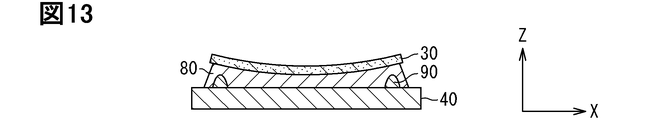
図13は、図12のXIII-XIII線に沿う断面図であり、半導体素子30とヒートシンク40との接続構造を示している。上記した電極構成において、半導体素子30は、図13に示すように下に凸の反りを生じうる。本実施形態では、はんだ80の最低膜厚を確保するように、はんだ80の供給量が設定されている。はんだ80は、半導体素子30(コレクタ電極32)とヒートシンク40との接合部を濡れ拡がった状態で、最低膜厚以上の所定の厚みを確保できるように供給される。図13に示すように、半導体素子30は、はんだ80に支持され、ワイヤ片90に対して非接触である。はんだ付け時において、半導体素子30は、溶融はんだに浮いている。はんだ80は、半導体素子30の凸先端、つまり素子中心と、ヒートシンク40との間のはんだ厚が最低膜厚を確保できるように、供給されている。図13は、ヒートシンク40に対する半導体素子30の配置に傾きのない理想的な状態を示している。
<Summary of Third Embodiment>
FIG. 13 is a cross-sectional view taken along line XIII-XIII of FIG. 12 and shows the connection structure between the semiconductor element 30 and the heat sink 40. As shown in FIG. In the electrode configuration described above, the semiconductor element 30 may warp downward as shown in FIG. In this embodiment, the supply amount of the solder 80 is set so as to ensure the minimum film thickness of the solder 80 . The solder 80 is supplied so as to ensure a predetermined thickness equal to or greater than the minimum film thickness while wetting and spreading the joint between the semiconductor element 30 (collector electrode 32 ) and the heat sink 40 . As shown in FIG. 13, semiconductor element 30 is supported by solder 80 and is not in contact with wire piece 90 . During soldering, the semiconductor element 30 floats on the molten solder. The solder 80 is supplied such that the solder thickness between the convex tip of the semiconductor element 30, that is, the center of the element, and the heat sink 40 can ensure a minimum film thickness. FIG. 13 shows an ideal state in which the semiconductor element 30 is arranged with respect to the heat sink 40 without inclination.

図14は、半導体素子30が傾いて配置されたときの断面図である。図14に示すように、下に凸の反りを生じた半導体素子30が傾いて配置された場合、半導体素子30は、複数のワイヤ片90の一部に接触する。ワイヤ片90が半導体素子30を支持することで、はんだ80の最低膜厚が確保される。ワイヤ片90は、反りが生じた半導体素子30が傾いて配置された場合に、はんだ80の最低膜厚を確保できる高さを有している。ワイヤ片90を外周領域80bの少なくとも四隅に配置しているため、半導体素子30がいずれの方向に傾いても、ワイヤ片90の少なくともひとつにより支持することができる。以上より、本実施形態の半導体装置10によれば、半導体素子30に下に凸の反りが生じても、はんだ80の膜厚を保証することができる。これにより、信頼性(接続信頼性)の高い半導体装置10を提供することができる。 FIG. 14 is a cross-sectional view when the semiconductor element 30 is tilted. As shown in FIG. 14 , when the semiconductor element 30 that is warped downward is tilted, the semiconductor element 30 comes into contact with part of the plurality of wire pieces 90 . By supporting the semiconductor element 30 with the wire piece 90, the minimum film thickness of the solder 80 is ensured. The wire piece 90 has a height that ensures the minimum film thickness of the solder 80 when the warped semiconductor element 30 is tilted. Since the wire pieces 90 are arranged at least at the four corners of the outer peripheral region 80b, the semiconductor element 30 can be supported by at least one of the wire pieces 90 even if it is tilted in any direction. As described above, according to the semiconductor device 10 of the present embodiment, the film thickness of the solder 80 can be guaranteed even if the semiconductor element 30 is warped downwardly. Thereby, the semiconductor device 10 with high reliability (connection reliability) can be provided.

半導体素子30が下に凸の反りを生じる電極構成は、上記した例に限定されない。 The electrode configuration that causes the semiconductor element 30 to warp downward is not limited to the above example.

外周領域80bにおいて、四隅とともに、四隅以外の部分にもワイヤ片90を配置してもよい。すなわち、素子中心30cを取り囲むように5つ以上のワイヤ片90bを配置してもよい。 In the outer peripheral region 80b, wire pieces 90 may be arranged not only at the four corners but also at portions other than the four corners. That is, five or more wire pieces 90b may be arranged to surround the element center 30c.

(第4実施形態)
この実施形態は、先行する実施形態を基礎的形態とする変形例であり、先行実施形態の記載を援用できる。
(Fourth embodiment)
This embodiment is a modification based on the preceding embodiment, and the description of the preceding embodiment can be used.

ワイヤ片90の延設方向は、第1対向面において特に制限されない。任意の方向に延設することができる。好ましくは、図15に示す所定の方向に、ワイヤ片90を延設するのとよい。図15は、本実施形態の半導体装置10において、半導体素子とヒートシンクとの接続部周辺を示す平面図である。図15は、図7に対応している。図15では、ワイヤ片90の明確化のため、半導体素子30を一点鎖線で示し、ワイヤ片90を実線で示している。半導体装置10の構成は、たとえば第1実施形態と同様である。図15に示す構成は、上アーム6H側と下アーム6L側とで同じである。 The extending direction of the wire piece 90 is not particularly limited on the first opposing surface. It can extend in any direction. Preferably, the wire piece 90 extends in the predetermined direction shown in FIG. FIG. 15 is a plan view showing the periphery of the connecting portion between the semiconductor element and the heat sink in the semiconductor device 10 of this embodiment. FIG. 15 corresponds to FIG. In FIG. 15, for clarity of wire piece 90, semiconductor element 30 is indicated by a dashed line, and wire piece 90 is indicated by a solid line. The configuration of the semiconductor device 10 is similar to that of the first embodiment, for example. The configuration shown in FIG. 15 is the same on the upper arm 6H side and the lower arm 6L side.

ワイヤ片90は、ヒートシンク40の実装面40aに固定されている。ワイヤ片90の個数および配置は、第1実施形態(図7参照)と同様である。本実施形態では、ワイヤ片90が、平面視において素子中心30cに向けて延びている。すなわち、ワイヤ片90の延設方向(長手方向)が、該ワイヤ片90と素子中心30cとを結ぶ仮想線に略平行である。ワイヤ片90は、この仮想線に沿って延びている。ワイヤ片90のうち、はんだ80の中央領域80aに配置された3つのワイヤ片90aは、いずれも素子中心30cに向けて延びている。はんだ80の外周領域80bに配置された4つのワイヤ片90bは、いずれも素子中心30cに向けて延びている。 The wire piece 90 is fixed to the mounting surface 40 a of the heat sink 40 . The number and arrangement of wire pieces 90 are the same as in the first embodiment (see FIG. 7). In this embodiment, the wire piece 90 extends toward the element center 30c in plan view. That is, the extending direction (longitudinal direction) of the wire piece 90 is substantially parallel to the imaginary line connecting the wire piece 90 and the element center 30c. Wire piece 90 extends along this imaginary line. Of the wire pieces 90, the three wire pieces 90a arranged in the central region 80a of the solder 80 all extend toward the element center 30c. All four wire pieces 90b arranged in the outer peripheral region 80b of the solder 80 extend toward the element center 30c.

<第4実施形態のまとめ>
本実施形態によれば、ワイヤ片90が素子中心30cに向けて延びているため、塗布した溶融はんだが濡れ拡がる際に、ワイヤ片90がその流れを阻害し難い。これにより、はんだ80にボイドが生じたり、対向面間に未充填部分が生じるのを抑制することができる。なお、複数のワイヤ片90の少なくともひとつを上記した延設方向とすることで、少なからず効果を奏することができる。本実施形態では、はんだ80に配置されたすべてのワイヤ片90が、素子中心30cに向けて延びている。これにより、上記した効果を高め、ひいては接続信頼性を高めることができる。
<Summary of the fourth embodiment>
According to this embodiment, since the wire piece 90 extends toward the element center 30c, the wire piece 90 is less likely to block the flow of the applied molten solder when it spreads. As a result, it is possible to suppress the occurrence of voids in the solder 80 and the occurrence of unfilled portions between the opposing surfaces. By setting at least one of the plurality of wire pieces 90 in the extending direction described above, not a little effect can be obtained. In this embodiment, all wire pieces 90 placed on solder 80 extend toward element center 30c. As a result, the above effects can be enhanced, and the connection reliability can be enhanced.

上記した関係を、第1実施形態の構成に適用する例を示したが、これに限定されない。たとえば、はんだ80に配置されるワイヤ片90の個数や配置が、第1実施形態とは異なる構成にも適用することができる。たとえば図16に示す変形例のように、第3実施形態(図12参照)の構成に適用してもよい。はんだ80の外周領域80bに配置されたワイヤ片90は、素子中心30cに向けて延びている。よって、第3実施形態に記載した効果を奏しつつ、接続信頼性を高めることができる。なお、複数のワイヤ片90の少なくともひとつを上記した延設方向とすることで、少なからず効果を奏することができる。図16では、外周領域80bに配置されたすべてのワイヤ片90が、素子中心30cに向けて延びている。よって、接続信頼性をより高めることができる。 Although an example in which the relationship described above is applied to the configuration of the first embodiment has been shown, the present invention is not limited to this. For example, the number and arrangement of the wire pieces 90 arranged on the solder 80 can be applied to a configuration different from that of the first embodiment. For example, like the modification shown in FIG. 16, it may be applied to the configuration of the third embodiment (see FIG. 12). A wire piece 90 arranged in the outer peripheral region 80b of the solder 80 extends toward the element center 30c. Therefore, connection reliability can be improved while exhibiting the effects described in the third embodiment. By setting at least one of the plurality of wire pieces 90 in the extending direction described above, not a little effect can be obtained. In FIG. 16, all wire segments 90 located in outer peripheral region 80b extend toward element center 30c. Therefore, connection reliability can be further improved.

また、延設方向の制御は、はんだ80内のワイヤ片90に限定されない。ワイヤ片90が配置されるはんだであれば適用が可能である。たとえば、はんだ81にワイヤ片90を配置する場合、このワイヤ片90に適用してもよい。はんだ82にワイヤ片90を配置する場合、このワイヤ片90に適用してもよい。また、上記した延設方向を、上アーム6H側および下アーム6L側の一方のみで満たすようにしてもよい。 Also, control of the extension direction is not limited to the wire piece 90 in the solder 80 . Any solder on which the wire piece 90 is arranged can be applied. For example, when a wire piece 90 is arranged on the solder 81, it may be applied to this wire piece 90. When a wire piece 90 is arranged on the solder 82, it may be applied to this wire piece 90. Also, the extension direction described above may be satisfied by only one of the upper arm 6H side and the lower arm 6L side.

また、はんだ歪を考慮すると、延設長さを以下のように設定するとよい。平面視において、ワイヤ片90の延設長さが所定長さ以下では、はんだ80の端部(外周端)においてはんだ歪が最大となる。一方、延設長さが所定長さを超えると、ワイヤ片90の端部においてはんだ歪が最大となる。延設長さが長くなるとワイヤ片端部のはんだ歪が増加し、所定長さを超えるとワイヤ片端部とはんだ端部とのはんだ歪の大小関係が逆転する。よって、ワイヤ片90の端部のはんだ歪が、はんだ80の端部のはんだ歪を超えない範囲で、延設長さを設定するのが好ましい。たとえばワイヤ片90を形成するアルミニウム系のボンディングワイヤの直径80μmに対し、ワイヤ片90の長さを350μm以下にするとよい。具体的には、200~350μmの範囲内で設定するとよい。 Considering solder distortion, the extension length should be set as follows. In a plan view, when the extension length of the wire piece 90 is equal to or less than a predetermined length, solder distortion is maximized at the end (peripheral end) of the solder 80 . On the other hand, when the extended length exceeds the predetermined length, the solder strain becomes maximum at the end of the wire piece 90 . As the extension length increases, the solder strain on the wire end increases, and when the length exceeds a predetermined length, the magnitude relationship of the solder strain between the wire end and the solder end is reversed. Therefore, it is preferable to set the extension length within a range in which the solder strain at the end of the wire piece 90 does not exceed the solder strain at the end of the solder 80 . For example, the length of the wire piece 90 should be 350 μm or less, while the aluminum-based bonding wire forming the wire piece 90 has a diameter of 80 μm. Specifically, it should be set within the range of 200 to 350 μm.

(第5実施形態)
この実施形態は、先行する実施形態を基礎的形態とする変形例であり、先行実施形態の記載を援用できる。
(Fifth embodiment)
This embodiment is a modification based on the preceding embodiment, and the description of the preceding embodiment can be used.

図17~図19に示すように、ワイヤ片90を、表面電極と表側配線部材とを接合するはんだ81に配置してもよい。その際、図17~図19に示す位置にワイヤ片90を配置するとよい。図17は、本実施形態の半導体装置10において、はんだ81に配置されたワイヤ片90と半導体素子30との位置関係を示している。図18は、ターミナル55におけるワイヤ片90の配置を示している。図19は、図17のXIX-XIX線に沿う断面図である。図19では、便宜上、ゲート配線34を省略して図示している。本実施形態の半導体装置10の構成は、たとえば第1実施形態と同様である。はんだ81に配置されたワイヤ片90の構成は、上アーム6H側と下アーム6L側とで同じである。 As shown in FIGS. 17-19, a piece of wire 90 may be placed in the solder 81 that joins the surface electrode and the front side wiring member. At that time, the wire piece 90 should be arranged at the positions shown in FIGS. FIG. 17 shows the positional relationship between the wire piece 90 arranged on the solder 81 and the semiconductor element 30 in the semiconductor device 10 of this embodiment. FIG. 18 shows the arrangement of wire pieces 90 in terminal 55. FIG. 19 is a cross-sectional view taken along line XIX-XIX in FIG. 17. FIG. In FIG. 19, the gate wiring 34 is omitted for the sake of convenience. The configuration of the semiconductor device 10 of this embodiment is similar to that of the first embodiment, for example. The configuration of the wire piece 90 arranged on the solder 81 is the same between the upper arm 6H side and the lower arm 6L side.

複数のワイヤ片90は、半導体素子30のエミッタ電極31とターミナル55の第1端面55aとの間のはんだ接合部に設けられている。複数のワイヤ片90は、そのすべてがターミナル55の第1端面55aに固定(接合)されており、半導体素子30のエミッタ電極31上、すなわち表面には固定されていない。ターミナル55の第1端面55aが第1対向面に相当し、半導体素子30の表面が第2対向面に相当する。第1端面55aには、複数のワイヤ片90が固定されている。第1端面55aに固定されたすべてのワイヤ片90が、はんだ81内に配置されている。 A plurality of wire pieces 90 are provided at the solder joint between the emitter electrode 31 of the semiconductor element 30 and the first end surface 55 a of the terminal 55 . All of the plurality of wire pieces 90 are fixed (bonded) to the first end surface 55a of the terminal 55, and are not fixed onto the emitter electrode 31 of the semiconductor element 30, that is, on the surface. The first end surface 55a of the terminal 55 corresponds to the first facing surface, and the surface of the semiconductor element 30 corresponds to the second facing surface. A plurality of wire pieces 90 are fixed to the first end face 55a. All wire pieces 90 fixed to the first end face 55a are arranged in the solder 81. As shown in FIG.

半導体素子30は、上記したようにゲートパッド33gを有している。半導体素子30は、表面側に形成され、ゲートパッド33gに連なるゲート配線34と、表面に形成された保護膜の一部分であり、ゲート配線34を保護するゲート配線保護部35を有している。エミッタ電極31はX方向において二分割され、隣り合うエミッタ電極31の間に、アルミニウム等を材料としてゲート配線34が形成されている。 The semiconductor element 30 has the gate pad 33g as described above. The semiconductor element 30 has a gate wiring 34 formed on the surface side and connected to a gate pad 33g, and a gate wiring protection portion 35 which is a part of a protective film formed on the surface and which protects the gate wiring 34 . The emitter electrode 31 is divided into two in the X direction, and a gate wiring 34 made of aluminum or the like is formed between the adjacent emitter electrodes 31 .

半導体素子30の表面には、ポリイミドなどを材料とする保護膜が形成されており、エミッタ電極31およびパッド33は保護膜から露出している。ゲート配線保護部35は、この保護膜の一部分であり、ゲート配線34を覆う部分である。図17では、ゲート配線保護部35のうち、平面視においてターミナル55と重なる部分を、破線の領域として示している。図18では、位置関係を示すため、ターミナル55の第1端面55aに、ゲート配線保護部35を一点鎖線の領域として示している。 A protective film made of polyimide or the like is formed on the surface of the semiconductor element 30, and the emitter electrode 31 and the pad 33 are exposed from the protective film. The gate wire protection portion 35 is a portion of this protective film and covers the gate wire 34 . In FIG. 17, the portion of the gate line protection portion 35 that overlaps with the terminal 55 in plan view is shown as a broken line region. In FIG. 18, in order to show the positional relationship, the gate line protection portion 35 is shown as a chain-dotted area on the first end surface 55a of the terminal 55. As shown in FIG.

ワイヤ片90は、平面視においてゲート配線保護部35と重ならない位置に配置されている。図17および図18に示すように、第1端面55aの中心付近であって、ゲート配線保護部35と重ならない位置に、ひとつのワイヤ片90が固定されている。また、平面略矩形状をなす第1端面55aの四隅のそれぞれに、ワイヤ片90が固定されている。このように、5つのワイヤ片90が第1端面55aに固定されている。 The wire piece 90 is arranged at a position not overlapping the gate wire protection portion 35 in plan view. As shown in FIGS. 17 and 18, one wire piece 90 is fixed near the center of the first end face 55a at a position that does not overlap the gate wire protection portion 35. As shown in FIGS. A wire piece 90 is fixed to each of the four corners of the first end face 55a, which has a substantially rectangular planar shape. Thus, five wire pieces 90 are fixed to the first end surface 55a.

<第5実施形態のまとめ>
本実施形態では、はんだ81内に複数のワイヤ片90を配置している。これにより、はんだ81の最低膜厚を確保することができる。
<Summary of the fifth embodiment>
In this embodiment, a plurality of wire pieces 90 are arranged within solder 81 . Thereby, the minimum film thickness of the solder 81 can be secured.

また、はんだ81内のワイヤ片90のすべてを、平面視においてゲート配線保護部35と重ならない位置に設けている。これにより、半導体装置10を形成する際に、ワイヤ片90がゲート配線保護部35に接触して保護膜を傷つけるのを抑制することができる。よって、保護膜の傷ついた部分からはんだ81がゲート配線34側に侵入し、ゲート電極とエミッタ電極31とのショート、すなわちゲートリーク不良が生じるのを抑制することができる。 Moreover, all of the wire pieces 90 in the solder 81 are provided at positions not overlapping the gate wiring protection portion 35 in plan view. As a result, when the semiconductor device 10 is formed, it is possible to prevent the wire piece 90 from contacting the gate wiring protection portion 35 and damaging the protection film. Therefore, it is possible to prevent the solder 81 from entering the gate wiring 34 side from the damaged portion of the protective film, thereby preventing the gate electrode and the emitter electrode 31 from short-circuiting, that is, gate leak failure.

エミッタ電極31はコレクタ電極32よりも面積が小さい。換言すれば、はんだ81の接合部は、平面視においてはんだ80の接合部よりも小さい。よって、半導体素子30に上に凸の反りが生じても、第1端面55aの中心付近に設けたひとつのワイヤ片90により、半導体素子30を支持することができる。これにより、はんだ81の最低膜厚を確保することができる。また、半導体素子30に下に凸の反りが生じても、四隅に配置されたワイヤ片90により半導体素子30を支持することができる。これにより、はんだ81の最低膜厚を確保することができる。以上より、信頼性の高い半導体装置10を提供することができる。 The emitter electrode 31 has a smaller area than the collector electrode 32 . In other words, the joint of solder 81 is smaller than the joint of solder 80 in plan view. Therefore, even if the semiconductor element 30 is warped upwardly, the semiconductor element 30 can be supported by the single wire piece 90 provided near the center of the first end surface 55a. Thereby, the minimum film thickness of the solder 81 can be secured. Further, even if the semiconductor element 30 is warped downwardly, the semiconductor element 30 can be supported by the wire pieces 90 arranged at the four corners. Thereby, the minimum film thickness of the solder 81 can be secured. As described above, a highly reliable semiconductor device 10 can be provided.

ワイヤ片90を、ターミナル55の第1端面55aに固定する例を示したがこれに限定されない。ワイヤ片90を、半導体素子30のエミッタ電極31に固定してもよい。すなわち、半導体素子30の表面を第1対向面としてもよい。しかしながら、ワイヤ片90をターミナル55(表側配線部材)に固定する構造のほうが、ワイヤ片90を接合する際の影響が小さいため、好ましい。 Although an example in which the wire piece 90 is fixed to the first end surface 55a of the terminal 55 is shown, the present invention is not limited to this. A piece of wire 90 may be fixed to the emitter electrode 31 of the semiconductor device 30 . That is, the surface of the semiconductor element 30 may be used as the first facing surface. However, the structure in which the wire piece 90 is fixed to the terminal 55 (front side wiring member) is preferable because the influence when the wire piece 90 is joined is small.

はんだ81におけるワイヤ片90の個数および配置は、上記した例に限定されない。平面視においてゲート配線保護部35と重ならない条件を満たす範囲で配置できる。たとえば第1端面55aの中心付近に複数のワイヤ片90を配置してもよい。また、第1端面55aの外周端近傍において、四隅とともに、四隅以外の部分にもワイヤ片90を配置してもよい。また、上記した配置を、上アーム6H側および下アーム6L側の一方のみで満たすようにしてもよい。 The number and arrangement of wire pieces 90 in solder 81 are not limited to the above example. It can be arranged within a range that satisfies the condition that it does not overlap with the gate wiring protection portion 35 in plan view. For example, a plurality of wire pieces 90 may be arranged near the center of the first end face 55a. Moreover, in the vicinity of the outer peripheral end of the first end surface 55a, the wire pieces 90 may be arranged not only at the four corners but also at portions other than the four corners. Also, the above-described arrangement may be satisfied with only one of the upper arm 6H side and the lower arm 6L side.

上記した関係を、第1実施形態の構成に適用する例を示したが、これに限定されない。はんだ81に配置されるワイヤ片90に、第2実施形態の構成、第3実施形態の構成、および第4実施形態の構成の少なくともひとつを組み合わせてもよい。たとえば、はんだ80に配置されるワイヤ片90の個数が、第1実施形態とは異なる個数の構成にも適用することができる。たとえば、はんだ80、81に配置されるワイヤ片90の数を同数としてもよい。 Although an example in which the relationship described above is applied to the configuration of the first embodiment has been shown, the present invention is not limited to this. At least one of the configuration of the second embodiment, the configuration of the third embodiment, and the configuration of the fourth embodiment may be combined with the wire piece 90 arranged on the solder 81 . For example, a configuration in which the number of wire pieces 90 arranged on the solder 80 is different from that of the first embodiment can also be applied. For example, the number of wire pieces 90 arranged on solders 80 and 81 may be the same.

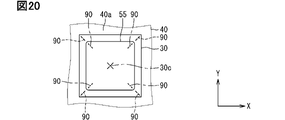
図20に示す変形例では、はんだ80における外周領域80bの四隅にワイヤ片90が配置され、はんだ81における四隅にワイヤ片90が配置されている。つまり、はんだ80、81にそれぞれ4つのワイヤ片90が配置されている。半導体素子30に下に凸の反りが生じても、はんだ81に配置されたワイヤ片90により半導体素子30を支持することができる。これにより、はんだ81の最低膜厚を確保することができる。はんだ81におけるワイヤ片90は、ゲート配線保護部35と重ならない位置に配置されている。はんだ80、81に配置された各ワイヤ片90は、図16に示した構成同様、素子中心30cに向けて延びている。図20は、ターミナル55を第2端面側から見た平面図である。図20では、はんだ80に配置されるワイヤ片90を破線、はんだ81に配置されるワイヤ片90を一点鎖線で示している。 In the modification shown in FIG. 20 , wire pieces 90 are arranged at the four corners of the outer peripheral region 80 b of the solder 80 and wire pieces 90 are arranged at the four corners of the solder 81 . That is, four wire pieces 90 are arranged on each of the solders 80 and 81 . Even if the semiconductor element 30 is warped downwardly, the semiconductor element 30 can be supported by the wire pieces 90 arranged on the solder 81 . Thereby, the minimum film thickness of the solder 81 can be secured. The wire piece 90 in the solder 81 is arranged at a position not overlapping the gate wiring protection portion 35 . Each wire piece 90 disposed on the solders 80, 81 extends toward the element center 30c as in the configuration shown in FIG. FIG. 20 is a plan view of the terminal 55 viewed from the second end face side. In FIG. 20, the wire piece 90 arranged on the solder 80 is indicated by a dashed line, and the wire piece 90 arranged on the solder 81 is indicated by a dashed line.

また、はんだ80にワイヤ片90を配置せず、上記したようにはんだ81にワイヤ片90を配置してもよい。本実施形態の構成は、裏側配線部材、すなわちヒートシンク40を備えない構成にも適用が可能である。 Further, the wire piece 90 may be arranged on the solder 81 as described above without arranging the wire piece 90 on the solder 80 . The configuration of this embodiment can also be applied to a configuration that does not include the back wiring member, that is, the heat sink 40 .

半導体装置10がターミナル55を備える例を示したが、これに限定されない。ターミナル55を備えない構成においても適用が可能である。たとえば、エミッタ電極31とヒートシンク50の実装面50aとのはんだ接合部において、ヒートシンク50の実装面50aにワイヤ片90を固定してもよい。 Although an example in which the semiconductor device 10 includes the terminals 55 has been shown, the present invention is not limited to this. A configuration without the terminal 55 is also applicable. For example, the wire piece 90 may be fixed to the mounting surface 50a of the heat sink 50 at the solder joint between the emitter electrode 31 and the mounting surface 50a of the heat sink 50. FIG.

(第6実施形態)
この実施形態は、先行する実施形態を基礎的形態とする変形例であり、先行実施形態の記載を援用できる。
(Sixth embodiment)
This embodiment is a modification based on the preceding embodiment, and the description of the preceding embodiment can be used.

はんだ80、81の両方にワイヤ片90を配置する場合、ワイヤ片90の配置は特に制限されない。図21に示すようにワイヤ片90を配置してもよい。図21は、本実施形態の半導体装置10において、ターミナルを第2端面側から見た平面図である。図21は、図7に対応している。半導体装置10の構成は、たとえば第1実施形態と同様である。図21に示す構成は、上アーム6H側と下アーム6L側とで同じである。 When the wire piece 90 is arranged on both solders 80 and 81, the arrangement of the wire piece 90 is not particularly limited. Wire pieces 90 may be arranged as shown in FIG. FIG. 21 is a plan view of the terminals of the semiconductor device 10 of the present embodiment as seen from the second end face side. FIG. 21 corresponds to FIG. The configuration of the semiconductor device 10 is similar to that of the first embodiment, for example. The configuration shown in FIG. 21 is the same on the upper arm 6H side and the lower arm 6L side.

半導体装置10は、はんだ80に配置された複数のワイヤ片90と、はんだ81に配置された複数のワイヤ片90を備えている。以下では、はんだ80に配置されたワイヤ片90をワイヤ片900、はんだ81に配置されたワイヤ片90をワイヤ片901と示すことがある。図21では、ワイヤ片900を破線、ワイヤ片901を一点鎖線で示している。 The semiconductor device 10 includes a plurality of wire pieces 90 arranged in solder 80 and a plurality of wire pieces 90 arranged in solder 81 . Hereinafter, the wire piece 90 arranged on the solder 80 may be referred to as a wire piece 900 , and the wire piece 90 arranged on the solder 81 may be referred to as a wire piece 901 . In FIG. 21, the wire piece 900 is indicated by a dashed line, and the wire piece 901 is indicated by a dashed line.

ワイヤ片900は、第1実施形態に記載のワイヤ片90(図7参照)と同様の配置となっている。ワイヤ片900は、たとえばヒートシンク40の実装面40aに固定されている。はんだ80の中央領域80aには、素子中心30cを取り囲むように3つのワイヤ片900が配置されている。外周領域80bには、半導体素子30の四隅のそれぞれに対応して4つのワイヤ片900が配置されている。 The wire piece 900 has the same arrangement as the wire piece 90 (see FIG. 7) described in the first embodiment. The wire piece 900 is fixed to the mounting surface 40a of the heat sink 40, for example. Three wire pieces 900 are arranged in the central region 80a of the solder 80 so as to surround the element center 30c. Four wire pieces 900 are arranged corresponding to the four corners of the semiconductor element 30 in the outer peripheral region 80b.

ワイヤ片901は、第5実施形態に記載のワイヤ片90(図17参照)と同様の配置となっている。ワイヤ片901は、たとえばターミナル55の第1端面55aに固定されている。第1端面55aの中心付近にひとつのワイヤ片901が配置されている。第1端面55aの四隅にワイヤ片901が配置されている。図21に示すように、ワイヤ片900とワイヤ片901とは、平面視において互いに重ならない位置に配置されている。 The wire piece 901 has the same arrangement as the wire piece 90 (see FIG. 17) described in the fifth embodiment. The wire piece 901 is fixed to the first end face 55a of the terminal 55, for example. One wire piece 901 is arranged near the center of the first end face 55a. Wire pieces 901 are arranged at the four corners of the first end face 55a. As shown in FIG. 21, the wire piece 900 and the wire piece 901 are arranged so as not to overlap each other in plan view.

<第6実施形態のまとめ>
図22は、比較例と本例(本実施形態)との違いを示す模式的な図である。比較例において、本実施形態(本例)の要素と同一又は関連する要素について、本実施形態の符号の末尾にrを付け加えて示している。図22では、便宜上、半導体素子の主電極を省略して図示している。
<Summary of the sixth embodiment>
FIG. 22 is a schematic diagram showing the difference between the comparative example and this example (this embodiment). In the comparative example, elements that are the same as or related to elements of this embodiment (this example) are indicated by adding r to the end of the reference numerals of this embodiment. For the sake of convenience, FIG. 22 omits the main electrodes of the semiconductor elements.

ワイヤ片900r、901rは、上記したようにアルミニウム系の材料を用いて形成されており、はんだ80r、81rに対する濡れ性が、半導体素子30rの図示しない主電極、ヒートシンク40r、およびターミナル55rよりも低い。このため、ワイヤ片900r、901rとはんだ80r、81rとの間に、空隙86rが形成される。空隙86rは熱伝導を妨げる。比較例のように、平面視においてワイヤ片900r、901rが重なると、空隙86rも重なる。半導体素子30rに対してZ方向の両側に空隙86rが存在するため、空隙86r(ワイヤ片900r、901r)と重なる半導体素子30rの部分からZ方向へ熱を逃がしにくい。よって、熱抵抗が増加する。 The wire pieces 900r and 901r are formed using an aluminum-based material as described above, and have lower wettability to the solders 80r and 81r than the main electrodes (not shown) of the semiconductor element 30r, the heat sink 40r, and the terminals 55r. . Therefore, gaps 86r are formed between the wire pieces 900r, 901r and the solders 80r, 81r. Air gap 86r impedes heat conduction. As in the comparative example, when the wire pieces 900r and 901r overlap in plan view, the gap 86r also overlaps. Since the gaps 86r exist on both sides of the semiconductor element 30r in the Z direction, it is difficult for heat to escape in the Z direction from the portions of the semiconductor element 30r overlapping the gaps 86r (wire pieces 900r and 901r). Therefore, thermal resistance increases.

本実施形態(本例)でも、比較例同様、ワイヤ片900とはんだ80との間、ワイヤ片901とはんだ81との間に、空隙86がそれぞれ形成される。しかしながら、ワイヤ片900、901が、平面視において互いに重ならない位置に配置されているため、はんだ80、81中の空隙86が、平面視において互いに重ならない、若しくは、重なってもごく一部である。よって、半導体素子30の熱をZ方向における少なくとも一方へ逃がすことができる。これにより、比較例に較べて熱抵抗を小さくし、放熱性を高めることができる。なお、他の実施形態では、空隙86を省略して図示している。 In this embodiment (this example) as well, gaps 86 are formed between the wire piece 900 and the solder 80 and between the wire piece 901 and the solder 81, respectively, as in the comparative example. However, since the wire pieces 900 and 901 are arranged at positions that do not overlap each other in plan view, the voids 86 in the solders 80 and 81 do not overlap each other in plan view, or if they do overlap, they are very small. . Therefore, the heat of the semiconductor element 30 can be released in at least one direction in the Z direction. As a result, the heat resistance can be reduced and the heat dissipation can be improved as compared with the comparative example. Note that in other embodiments, the air gap 86 is omitted in the illustration.

本実施形態では、ワイヤ片900が、第1実施形態と同様の構成となっている。このため、本実施形態に記載の効果に加え、第1実施形態に記載の効果も奏することができる。また、ワイヤ片901が、第5実施形態と同様の構成配置となっている。このため、本実施形態に記載の効果に加え、第5実施形態に記載の効果も奏することができる。しかしながら、ワイヤ片900、901の個数、配置は、平面視においてワイヤ片900、901が互いに重ならない条件を満たす範囲内で選択が可能である。すなわち、個数および配置は、上記した例に限定されない。 In this embodiment, the wire piece 900 has the same configuration as in the first embodiment. Therefore, in addition to the effects described in this embodiment, the effects described in the first embodiment can also be achieved. Also, the wire piece 901 has the same configuration and arrangement as in the fifth embodiment. Therefore, in addition to the effects described in this embodiment, the effects described in the fifth embodiment can also be achieved. However, the number and arrangement of the wire pieces 900 and 901 can be selected within a range that satisfies the condition that the wire pieces 900 and 901 do not overlap each other in plan view. That is, the number and arrangement are not limited to the above examples.

たとえば、ワイヤ片900のみ第1実施形態同様の構成とし、ワイヤ片901は第5実施形態とは異なる構成としてもよい。ワイヤ片901のみ第4実施形態同様の構成とし、ワイヤ片900は第1実施形態とは異なる構成としてもよい。また、ワイヤ片900、901を同数としてもよい。図20に示した構成では、はんだ80、81のワイヤ片90が同数である。ワイヤ片900に相当するはんだ80側のワイヤ片90と、ワイヤ片901に相当するはんだ81側のワイヤ片90とが、平面視において互いに重ならない位置に配置されている。 For example, only the wire piece 900 may have the same configuration as in the first embodiment, and the wire piece 901 may have a different configuration from that in the fifth embodiment. Only the wire piece 901 may have the same configuration as in the fourth embodiment, and the wire piece 900 may have a different configuration from that in the first embodiment. Alternatively, the same number of wire pieces 900 and 901 may be used. In the configuration shown in FIG. 20, the solders 80, 81 have the same number of wire segments 90. In the configuration shown in FIG. The wire piece 90 on the solder 80 side corresponding to the wire piece 900 and the wire piece 90 on the solder 81 side corresponding to the wire piece 901 are arranged at positions that do not overlap each other in plan view.

ワイヤ片900をヒートシンク40に固定する例を示したが、半導体素子30の裏面(コレクタ電極32)に固定してもよい。ワイヤ片901をターミナル55に固定する例を示したが、半導体素子30の表面(エミッタ電極31)に固定してもよい。ワイヤ片900をヒートシンク40に固定し、ワイヤ片901を半導体素子30に固定してもよい。また、ワイヤ片900を半導体素子30に固定し、ワイヤ片901をターミナル55に固定してもよい。また、ターミナル55を備えない構成としてもよい。この場合、ワイヤ片901は、ヒートシンク50と半導体素子30(エミッタ電極31)とのはんだ接合部に設けられる。 Although an example in which the wire piece 900 is fixed to the heat sink 40 is shown, it may be fixed to the back surface of the semiconductor element 30 (collector electrode 32). Although an example of fixing the wire piece 901 to the terminal 55 has been shown, it may be fixed to the surface of the semiconductor element 30 (emitter electrode 31). Wire piece 900 may be fixed to heat sink 40 and wire piece 901 may be fixed to semiconductor device 30 . Alternatively, the wire piece 900 may be fixed to the semiconductor element 30 and the wire piece 901 may be fixed to the terminal 55 . Alternatively, a configuration without the terminal 55 may be employed. In this case, the wire piece 901 is provided at the solder joint between the heat sink 50 and the semiconductor element 30 (emitter electrode 31).

本実施形態の構成と、第2実施形態の構成、第3実施形態の構成、および第4実施形態の構成の少なくともひとつを組み合わせてもよい。ワイヤ片900、901の少なくとも一方に、第2実施形態の構成を組み合わせてもよい。ワイヤ片900、901の少なくとも一方に、第3実施形態の構成を組み合わせてもよい。ワイヤ片900、901の少なくとも一方に、第4実施形態の構成を組み合わせてもよい。また、本実施形態の構成を、上アーム6H側および下アーム6L側の一方のみで満たすようにしてもよい。 At least one of the configuration of this embodiment, the configuration of the second embodiment, the configuration of the third embodiment, and the configuration of the fourth embodiment may be combined. At least one of the wire pieces 900 and 901 may be combined with the configuration of the second embodiment. At least one of the wire pieces 900 and 901 may be combined with the configuration of the third embodiment. At least one of the wire pieces 900 and 901 may be combined with the configuration of the fourth embodiment. Also, the configuration of this embodiment may be satisfied with only one of the upper arm 6H side and the lower arm 6L side.

(第7実施形態)
この実施形態は、先行する実施形態を基礎的形態とする変形例であり、先行実施形態の記載を援用できる。
(Seventh embodiment)
This embodiment is a modification based on the preceding embodiment, and the description of the preceding embodiment can be used.

図23に示すように、ワイヤ片90を、はんだ82に配置してもよい。その際、各はんだ80、81、82のワイヤ片90を、図24に示すように配置するとよい。図23は、本実施形態の半導体装置10において、ヒートシンク40、50間の積層体を示す模式的な断面図である。図24は、各はんだ80、81、82におけるワイヤ片90の好ましい配置の一例を示す平面図である。図24は、図21に対応している。図24では、ワイヤ片900を破線、ワイヤ片901を一点鎖線で示している。本実施形態の半導体装置10の構成は、たとえば第1実施形態と同様である。図23および図24に示す構成は、上アーム6H側と下アーム6L側とでほぼ同じである。 A piece of wire 90 may be placed on the solder 82 as shown in FIG. At that time, the wire pieces 90 of each solder 80, 81, 82 should be arranged as shown in FIG. FIG. 23 is a schematic cross-sectional view showing a laminate between heat sinks 40 and 50 in the semiconductor device 10 of this embodiment. FIG. 24 is a plan view showing an example of preferred arrangement of wire pieces 90 in each solder 80, 81, 82. FIG. FIG. 24 corresponds to FIG. In FIG. 24, the wire piece 900 is indicated by a dashed line, and the wire piece 901 is indicated by a one-dot chain line. The configuration of the semiconductor device 10 of this embodiment is similar to that of the first embodiment, for example. The configurations shown in FIGS. 23 and 24 are substantially the same on the upper arm 6H side and the lower arm 6L side.

図23に示すように、はんだ80、81、82のそれぞれに複数のワイヤ片90が配置されている。以下では、はんだ80に配置されたワイヤ片90をワイヤ片900、はんだ81に配置されたワイヤ片90をワイヤ片901、はんだ82に配置されたワイヤ片90をワイヤ片902と示すことがある。ワイヤ片90の個数は、はんだ80、81、82において互いに異なっている。ワイヤ片900が最も多く、ワイヤ片902が最も少ない。ワイヤ片901は、ワイヤ片900よりも少なく、ワイヤ片902よりも多い。 As shown in FIG. 23, a plurality of wire pieces 90 are arranged on each of the solders 80, 81, 82. As shown in FIG. Hereinafter, the wire piece 90 arranged on the solder 80 may be referred to as a wire piece 900, the wire piece 90 arranged on the solder 81 as a wire piece 901, and the wire piece 90 arranged on the solder 82 as a wire piece 902. The number of wire pieces 90 differs in solders 80 , 81 , 82 . Wire pieces 900 are the most and wire pieces 902 are the least. Wire segments 901 are less than wire segments 900 and more than wire segments 902 .

図23では、ワイヤ片900がヒートシンク40に固定されている。また、ワイヤ片901がターミナル55の第1端面55aに固定され、ワイヤ片902が第2端面55bに固定されている。 In FIG. 23, a piece of wire 900 is secured to heat sink 40 . A wire piece 901 is fixed to the first end face 55a of the terminal 55, and a wire piece 902 is fixed to the second end face 55b.

図24に示すように、ワイヤ片900は、第1実施形態に記載のワイヤ片90(図7参照)と同様の配置となっている。ワイヤ片900は、ヒートシンク40の実装面40aに固定されている。はんだ80の中央領域80aには、素子中心30cを取り囲むように3つのワイヤ片900が配置されている。外周領域80bには、半導体素子30の四隅のそれぞれに対応して4つのワイヤ片900が配置されている。 As shown in FIG. 24, the wire piece 900 has the same arrangement as the wire piece 90 (see FIG. 7) described in the first embodiment. The wire piece 900 is fixed to the mounting surface 40 a of the heat sink 40 . Three wire pieces 900 are arranged in the central region 80a of the solder 80 so as to surround the element center 30c. Four wire pieces 900 are arranged corresponding to the four corners of the semiconductor element 30 in the outer peripheral region 80b.

ワイヤ片901は、第5実施形態に記載のワイヤ片90(図17参照)と同様の配置となっている。ワイヤ片901は、ターミナル55の第1端面55aに固定されている。第1端面55aの中心付近にひとつのワイヤ片901が配置されている。第1端面55aの四隅にワイヤ片901が配置されている。 The wire piece 901 has the same arrangement as the wire piece 90 (see FIG. 17) described in the fifth embodiment. A wire piece 901 is fixed to the first end surface 55 a of the terminal 55 . One wire piece 901 is arranged near the center of the first end face 55a. Wire pieces 901 are arranged at the four corners of the first end face 55a.

ワイヤ片902は、ターミナル55の第2端面55bに固定されている。第2端面55bには、3つのワイヤ片902が固定されている。複数のワイヤ片902は、素子中心30cを取り囲むように配置されている。図24に示すように、ワイヤ片900、901、902は、平面視において互いに重ならない位置に配置されている。なお、ターミナル55が第1配線部材に相当し、ヒートシンク50が第2配線部材に相当する。はんだ81が、表側接合部材である第1接合部材に相当し、はんだ82が第2接合部材に相当する。 Wire piece 902 is fixed to second end surface 55 b of terminal 55 . Three wire pieces 902 are fixed to the second end face 55b. A plurality of wire pieces 902 are arranged to surround the element center 30c. As shown in FIG. 24, wire pieces 900, 901, and 902 are arranged at positions that do not overlap each other in plan view. The terminal 55 corresponds to the first wiring member, and the heat sink 50 corresponds to the second wiring member. The solder 81 corresponds to the first joint member, which is the front joint member, and the solder 82 corresponds to the second joint member.

<第7実施形態のまとめ>
本実施形態では、はんだ82に複数のワイヤ片90が配置されている。これにより、はんだ82の最低膜厚を確保することができる。また、はんだ80、81、82のそれぞれに、複数のワイヤ片90が配置されている。これにより、半導体素子30からZ方向両側のヒートシンク40、50までの電気伝導経路、熱伝導経路を構成するはんだ80、81、82のすべてについて、最低膜厚を確保することができる。
<Summary of the seventh embodiment>
In this embodiment, a plurality of wire pieces 90 are arranged on the solder 82 . Thereby, the minimum film thickness of the solder 82 can be secured. A plurality of wire pieces 90 are arranged on each of the solders 80 , 81 , 82 . As a result, the minimum film thickness can be ensured for all of the solders 80, 81, 82 forming the electrical and thermal conduction paths from the semiconductor element 30 to the heat sinks 40, 50 on both sides in the Z direction.

本実施形態では、はんだ80、81、82ごとにワイヤ片90の配置数が異なっている。電極面積の大きいコレクタ電極32側のはんだ80に、最も多いワイヤ片90(ワイヤ片900)が配置されている。また、コレクタ電極32よりも電極面積が小さいエミッタ電極31側において、半導体素子30に近い側のはんだ81に、ワイヤ片900よりも少ない数のワイヤ片90(ワイヤ片901)が配置されている。また、半導体素子30に対して遠い側のはんだ82には、最も少ないワイヤ片90(ワイヤ片902)が配置されている。具体的には、半導体装置10が、ワイヤ片90として、7つのワイヤ片900と、5つのワイヤ片901と、3つのワイヤ片902を備えている。 In this embodiment, the number of wire pieces 90 arranged is different for each solder 80 , 81 , 82 . The largest number of wire pieces 90 (wire pieces 900) are arranged on the solder 80 on the side of the collector electrode 32 having a large electrode area. Further, wire pieces 90 (wire pieces 901 ) less than the wire pieces 900 are arranged on the solder 81 closer to the semiconductor element 30 on the side of the emitter electrode 31 having an electrode area smaller than that of the collector electrode 32 . In addition, the smallest number of wire pieces 90 (wire pieces 902 ) are arranged on the solder 82 on the far side from the semiconductor element 30 . Specifically, the semiconductor device 10 includes seven wire pieces 900 , five wire pieces 901 and three wire pieces 902 as the wire pieces 90 .

はんだ80、81は、半導体素子30の反りの影響がある。コレクタ電極32に接続されることで平面視の面積が最も大きいはんだ80に、最も多いワイヤ片90を配置するため、はんだ80の最低膜厚を確保することができる。ワイヤ片900の配置を第1実施形態と同様とすることで、半導体素子30の反りに対しても最低膜厚を確保することができる。はんだ81は、コレクタ電極32よりも面積の小さいエミッタ電極31と、金属ブロック体であるターミナル55とを接続している。中心付近にひとつのワイヤ片90を設けることで、半導体素子30の上に凸の反りに対応することができる。はんだ80よりも少ないワイヤ片90の配置にて、はんだ81の最低膜厚を確保することができる。ワイヤ片901の配置を第5実施形態と同様とすることで、半導体素子30の反りに対しても最低膜厚を確保することができる。 Solders 80 and 81 are affected by warpage of semiconductor element 30 . Since the largest number of wire pieces 90 are arranged on the solder 80 that is connected to the collector electrode 32 and has the largest area in plan view, the minimum film thickness of the solder 80 can be ensured. By arranging the wire pieces 900 in the same manner as in the first embodiment, the minimum film thickness can be ensured against warpage of the semiconductor element 30 . The solder 81 connects the emitter electrode 31 having an area smaller than that of the collector electrode 32 and the terminal 55 which is a metal block. By providing one wire piece 90 in the vicinity of the center, it is possible to cope with the upwardly convex warp of the semiconductor element 30 . The minimum film thickness of the solder 81 can be ensured by arranging the wire pieces 90 less than the solder 80 . By arranging the wire pieces 901 in the same manner as in the fifth embodiment, the minimum film thickness can be ensured against warpage of the semiconductor element 30 .

はんだ82は、ターミナル55とヒートシンク50とを接続している。ターミナル55およびヒートシンク50には、半導体素子30のような反りは生じない。また、半導体素子30との間にターミナル55が存在するため、半導体素子30の反りの影響を受けない。よって、最も少ないワイヤ片90にて、はんだ82の最低膜厚を確保することができる。ワイヤ片901、902の数をワイヤ片900よりも少なくすることで、ワイヤ片900と同数の構成に較べて、はんだ81、82中の空隙86を低減することができる。よって、最低膜厚を確保しつつ、放熱性を高めることができる。さらに、ワイヤ片902の数をワイヤ片901よりも少なくするため、ワイヤ片901と同数の構成に較べて、放熱性を高めることができる。また、半導体装置10全体のワイヤ片90の個数を低減することもできる。 Solder 82 connects terminal 55 and heat sink 50 . Terminals 55 and heat sink 50 do not warp like semiconductor element 30 . In addition, since the terminal 55 exists between the semiconductor element 30 and the semiconductor element 30, the semiconductor element 30 is not affected by warping. Therefore, the minimum film thickness of the solder 82 can be ensured with the smallest number of wire pieces 90 . By using fewer wire pieces 901 and 902 than wire pieces 900 , voids 86 in solders 81 and 82 can be reduced compared to a configuration with the same number of wire pieces 900 . Therefore, heat dissipation can be improved while ensuring the minimum film thickness. Furthermore, since the number of wire pieces 902 is smaller than that of wire pieces 901, heat dissipation can be improved compared to a configuration in which the number of wire pieces 901 is the same. Also, the number of wire pieces 90 in the entire semiconductor device 10 can be reduced.

また、ワイヤ片900、901、902は、平面視において互いに重ならない位置に配置されている。Z方向において空隙86が互いに重ならない、若しくは、重なってもごく一部であるため、放熱性を高めることができる。 Also, the wire pieces 900, 901, and 902 are arranged at positions that do not overlap each other in plan view. Since the air gaps 86 do not overlap each other in the Z direction, or even if they overlap only partially, the heat dissipation can be improved.

はんだ80、81、82においてワイヤ片90の数を互いに異ならせる場合、その個数は上記した例に限定されない。ワイヤ片900の数>ワイヤ片901の数>ワイヤ片902の数、の関係を満たせばよい。なお、ワイヤ片900の数>ワイヤ片901の数=ワイヤ片902の数としてもよい。ワイヤ片900の数=ワイヤ片901の数>ワイヤ片902の数としてもよい。はんだ80、81、82の一部のワイヤ片90を、残りのワイヤ片90と異ならせることにより、効果は弱まるが、放熱性の向上およびワイヤ片90の低減を図ることができる。 When the solders 80, 81, 82 have different numbers of wire pieces 90, the number is not limited to the above example. The relationship of the number of wire pieces 900>the number of wire pieces 901>the number of wire pieces 902 should be satisfied. Alternatively, the number of wire pieces 900 > the number of wire pieces 901 = the number of wire pieces 902 may be satisfied. The number of wire pieces 900 may be equal to the number of wire pieces 901 >the number of wire pieces 902 . By making the wire pieces 90 of some of the solders 80, 81, 82 different from the remaining wire pieces 90, heat dissipation can be improved and the wire pieces 90 can be reduced, although the effect is weakened.

各はんだ80、81、82において最低膜厚を確保するのであれば、ワイヤ片90の数はより自由に設定できる。はんだ80、81、82においてワイヤ片90を同数としてもよい。それぞれに複数、好ましくは3つ以上のワイヤ片90を配置することで、はんだ厚を確保しやすくなる。 The number of wire pieces 90 can be set more freely if the minimum film thickness is ensured for each solder 80, 81, 82. FIG. The same number of wire pieces 90 may be used in the solders 80 , 81 , 82 . By arranging a plurality of wire pieces 90, preferably three or more wire pieces 90, it becomes easier to secure the solder thickness.

また、本実施形態の構成を、上アーム6H側および下アーム6L側の一方のみで満たすようにしてもよい。ワイヤ片90を、はんだ80、81、82に配置する例を示したが、さらにはんだ83、84の少なくとも一方に配置してもよい。 Also, the configuration of this embodiment may be satisfied with only one of the upper arm 6H side and the lower arm 6L side. Although an example in which the wire piece 90 is arranged on the solders 80, 81, 82 has been shown, it may be arranged on at least one of the solders 83, 84 as well.

(第8実施形態)
この実施形態は、先行する実施形態を基礎的形態とする変形例であり、先行実施形態の記載を援用できる。
(Eighth embodiment)
This embodiment is a modification based on the preceding embodiment, and the description of the preceding embodiment can be used.

ターミナル55の形状は特に限定されない。好ましくは、ワイヤ片90を、図25に本例として示す形状にするとよい。図25は、ターミナルについて比較例と本例(本実施形態)との違いを示す模式的な図である。比較例において、本実施形態(本例)の要素と同一又は関連する要素について、本実施形態の符号の末尾にrを付け加えて示している。比較例、本例ともに紙面上方が側面図、A面視の平面図である。本実施形態の半導体装置10は、たとえば第1実施形態と同様である。図25に示す構成は、上アーム6H側と下アーム6L側とでほぼ同じである。 The shape of the terminal 55 is not particularly limited. Preferably, the wire piece 90 has the shape shown in FIG. 25 as an example. FIG. 25 is a schematic diagram showing the difference between the comparative example and the present example (present embodiment) of the terminal. In the comparative example, elements that are the same as or related to elements of this embodiment (this example) are indicated by adding r to the end of the reference numerals of this embodiment. In both the comparative example and the present example, the upper side of the paper surface is a side view, and the plan view as viewed from the A side. The semiconductor device 10 of this embodiment is similar to, for example, the first embodiment. The configuration shown in FIG. 25 is substantially the same on the upper arm 6H side and the lower arm 6L side.

ターミナルは、プレス加工により金属板から打ち抜いて形成される。ワイヤ片は、ターミナルの端面をカメラで撮像して端面の角部を認識し、角部を位置基準として所定位置にボンディングワイヤを超音波接合することで形成される。比較例のターミナル55rは、Z方向における一方の端面の角に、打ち抜きによるR部550rを有する。このため、R部550r側の端面にワイヤ片90rを形成する際、R部550rがない側の端面に較べて、ワイヤ片90rの形成位置の精度が低くなる虞がある。 The terminal is formed by punching out from a metal plate by press working. The wire piece is formed by imaging the end face of the terminal with a camera, recognizing the corner of the end face, and ultrasonically bonding the bonding wire to a predetermined position using the corner as a position reference. A terminal 55r of the comparative example has a punched R portion 550r at a corner of one end face in the Z direction. Therefore, when the wire piece 90r is formed on the end face on the side of the R portion 550r, there is a possibility that the positional accuracy of forming the wire piece 90r may be lower than that on the end face on the side without the R portion 550r.

本実施形態(本例)でも、打ち抜いた状態のターミナル55は、比較例同様、一方の端面の角に図示しないR部を有する。しかしながら、打ち抜き後に、R部の面取り、たとえばC面取りを行う。C面取りとは、面取り角度が略45度の面取りである。ターミナル55は、面取り部550を有する。 In this embodiment (this example) as well, the punched terminal 55 has an R portion (not shown) at the corner of one end face, as in the comparative example. However, after punching, the R portion is chamfered, for example, C-chamfered. C-chamfering is chamfering with a chamfering angle of approximately 45 degrees. Terminal 55 has a chamfered portion 550 .

<第8実施形態のまとめ>
上記したように、本実施形態のターミナル55は、面取り部550を有している。このため、打ち抜き時にR部が形成される側の端面にワイヤ片90を形成する際、撮像により角部を精度よく認識することができる。よって、ワイヤ片90を位置精度よく形成することができる。
<Summary of the eighth embodiment>
As described above, the terminal 55 of this embodiment has the chamfered portion 550 . Therefore, when the wire piece 90 is formed on the end surface on which the R portion is formed during punching, the corner portion can be accurately recognized by imaging. Therefore, the wire piece 90 can be formed with high positional accuracy.

本実施形態の構成は、ターミナル55を備える構成において適用が可能である。先行実施形態のそれぞれとの組み合わせが可能である。また、ワイヤ片90の接続対象は、ターミナル55に限定されない。金属板を打ち抜いて形成され、打ち抜き時にR部が形成される部材について適用が可能である。打ち抜き後にR部を面取りすることで、打ち抜き時にR部が形成される側の面に、ワイヤ片90を位置精度よく形成することができる。 The configuration of this embodiment can be applied to a configuration including terminals 55 . Combinations with each of the preceding embodiments are possible. Also, the connection target of the wire piece 90 is not limited to the terminal 55 . It can be applied to a member that is formed by punching a metal plate and that has an R portion formed during the punching. By chamfering the R portion after punching, the wire piece 90 can be formed with high positional accuracy on the surface on which the R portion is formed during punching.

(第9実施形態)
この実施形態は、先行する実施形態を基礎的形態とする変形例であり、先行実施形態の記載を援用できる。この実施形態では、ワイヤ片90の構造および製造方法に特徴がある。
(Ninth embodiment)
This embodiment is a modification based on the preceding embodiment, and the description of the preceding embodiment can be used. This embodiment is characterized by the structure and manufacturing method of the wire piece 90 .

ワイヤ片90は、上記したように、アルミニウム系のボンディングワイヤを超音波接合し、1stボンドを行った時点でワイヤカットすることで形成される。このようなワイヤ片90として、好ましい形態のひとつを、図26~図29に示す。 As described above, the wire piece 90 is formed by ultrasonically bonding an aluminum-based bonding wire and cutting the wire when the 1st bond is performed. One preferred form of such a wire piece 90 is shown in FIGS. 26 to 29. FIG.

図26は、本実施形態の半導体装置10において、半導体素子30とヒートシンク40との接続構造を示している。図27は、図26のXXVII-XXVII線に沿う断面図である。図28は、図26および図27に適用しているワイヤ片90を示す斜視図である。図29は、ワイヤ片90の別例を示している。図26および図27では、ワイヤ片90の数を3つにしている。図26、図27、および図28では、便宜上、主電極の図示を省略している。本実施形態の半導体装置10は、たとえば第1実施形態と同様である。図26~図28に示す構成は、上アーム6H側と下アーム6L側とでほぼ同じである。 FIG. 26 shows a connection structure between the semiconductor element 30 and the heat sink 40 in the semiconductor device 10 of this embodiment. 27 is a cross-sectional view taken along line XXVII-XXVII of FIG. 26. FIG. FIG. 28 is a perspective view showing the wire piece 90 applied to FIGS. 26 and 27. FIG. FIG. 29 shows another example of wire piece 90 . 26 and 27, the number of wire pieces 90 is three. 26, 27 and 28 omit illustration of the main electrode for convenience. The semiconductor device 10 of this embodiment is similar to, for example, the first embodiment. The configurations shown in FIGS. 26 to 28 are substantially the same on the upper arm 6H side and the lower arm 6L side.

半導体素子30は、図示しないエミッタ電極31が形成された表面30aと、図示しないコレクタ電極32が形成された裏面30bを有している。コレクタ電極32が裏面30bをなしている。図21および図22に示すように、はんだ80に複数のワイヤ片90が配置されている。ワイヤ片90は、ヒートシンク40の実装面40aに接合(固定)されている。実装面40aが、配線部材における固定面に相当する。ワイヤ片90は、実装面40aから裏面30bに向けて突起している。ワイヤ片90は、ヒートシンク40に保持されている。このため、ヒートシンク40は、保持体と称されることがある。ワイヤ片90は、固定部91と、平坦部92と、非固定部93を有している。固定部91は、ワイヤ片90のヒートシンク40と対向する側において、ヒートシンク40との固定部分(接合箇所)である。 The semiconductor element 30 has a front surface 30a formed with an emitter electrode 31 (not shown) and a rear surface 30b formed with a collector electrode 32 (not shown). A collector electrode 32 forms the back surface 30b. As shown in FIGS. 21 and 22, solder 80 has a plurality of wire pieces 90 disposed thereon. The wire piece 90 is joined (fixed) to the mounting surface 40 a of the heat sink 40 . The mounting surface 40a corresponds to the fixing surface of the wiring member. The wire piece 90 protrudes from the mounting surface 40a toward the back surface 30b. Wire piece 90 is held by heat sink 40 . For this reason, the heat sink 40 is sometimes called a holder. The wire piece 90 has a fixed portion 91 , a flat portion 92 and a non-fixed portion 93 . The fixed portion 91 is a fixed portion (joint portion) to the heat sink 40 on the side of the wire piece 90 facing the heat sink 40 .

平坦部92は、ワイヤ片90において、半導体素子30の裏面30bと対向する側に形成され、ヒートシンクの実装面40aと略平行な部分である。非固定部93は、ワイヤ片90のヒートシンク40と対向する側において、固定部91に連なり、ヒートシンク40に固定されていない部分である。非固定部93は、Z方向において実装面40aから離れている。非固定部93は、固定部91を基準として浮いている。ワイヤ片90は、Z方向に弾性変形可能に設けられている。非固定部93と実装面40aとの隙間には、はんだ80が入り込んでいる。ワイヤ片90は、Z方向においてヒートシンク40側に固定部91および非固定部93を有し、固定部91および非固定部93とは反対側に平坦部92を有している。 The flat portion 92 is a portion of the wire piece 90 formed on the side facing the back surface 30b of the semiconductor element 30 and substantially parallel to the mounting surface 40a of the heat sink. The non-fixed portion 93 is a portion that continues to the fixed portion 91 and is not fixed to the heat sink 40 on the side of the wire piece 90 facing the heat sink 40 . The non-fixed portion 93 is separated from the mounting surface 40a in the Z direction. The non-fixed portion 93 floats on the basis of the fixed portion 91 . The wire piece 90 is provided so as to be elastically deformable in the Z direction. Solder 80 enters the gap between the non-fixed portion 93 and the mounting surface 40a. The wire piece 90 has a fixed portion 91 and a non-fixed portion 93 on the side of the heat sink 40 in the Z direction, and a flat portion 92 on the side opposite to the fixed portion 91 and the non-fixed portion 93 .

ワイヤ片90は、X方向に延設されている。図27および図28に示すワイヤ片90は、延設方向の両端に、平坦部92および非固定部93を有している。平坦部92は、平面視において非固定部93と重なる位置に設けられている。実装面40aから両端の平坦部92までの高さは、互いに略等しい。ワイヤ片90は、ZX平面において略U字状、若しくは、略C字状をなしている。両端の平坦部92は、半導体素子30の裏面30bにそれぞれ接触している。 The wire piece 90 extends in the X direction. A wire piece 90 shown in FIGS. 27 and 28 has flat portions 92 and non-fixed portions 93 at both ends in the extending direction. The flat portion 92 is provided at a position overlapping the non-fixed portion 93 in plan view. The heights from the mounting surface 40a to the flat portions 92 at both ends are substantially equal. The wire piece 90 is substantially U-shaped or substantially C-shaped in the ZX plane. The flat portions 92 at both ends are in contact with the rear surface 30b of the semiconductor element 30, respectively.

図29は、ワイヤ片90の別例を示している。このワイヤ片90は、両端ではなく、延設方向の一端にのみ平坦部92を有している。非固定部93は、延設方向の両端に設けられている。ワイヤ片90において、実装面40aから両端の上部までの高さが異なっている。平坦部92は、実装面40aからの突起高さが高い側の端部に形成されている。ワイヤ片90は、ZX平面において略J字状をなしている。平坦部92、図示しない素子中心30cに対して遠い側の端部に形成されている。 FIG. 29 shows another example of wire piece 90 . This wire piece 90 has a flat portion 92 only at one end in the extending direction, not at both ends. The non-fixed portions 93 are provided at both ends in the extending direction. In the wire piece 90, heights from the mounting surface 40a to the top of both ends are different. The flat portion 92 is formed at the end of the side where the height of the protrusion from the mounting surface 40a is high. The wire piece 90 is substantially J-shaped in the ZX plane. A flat portion 92 is formed at the far end of the element center 30c (not shown).

<製造方法>
次に、半導体装置10の製造方法、特に半導体素子30とヒートシンク40との接続体の製造方法について説明する。ここでは、図29に示したワイヤ片90の例を示す。
<Manufacturing method>
Next, a method for manufacturing the semiconductor device 10, particularly a method for manufacturing a connecting body between the semiconductor element 30 and the heat sink 40 will be described. Here, an example of the wire piece 90 shown in FIG. 29 is shown.

先ず、図30に示すように、ヒートシンク40の実装面40aにワイヤ片90を形成する。図示しないツールからの超音波により、ボンディングワイヤをヒートシンク40に接合し、固定部91を形成する。この固定部91は、1stボンド部である。そして、超音波の印加完了後に、固定部91に対して延設方向前後に非固定部93が残るようにボンディングワイヤを切断する。このように、2ndボンド部を形成せずに、ボンディングワイヤを切断する。1stボンド側のみを用いてワイヤ片90を形成するため、2点の接合体、すなわち1stボンド部と2ndボンド部を有する構造に較べて、形成時間を短縮することができる。また、ワイヤ片90の体格を小型化、たとえば延設長さを短くすることができる。よって、上記したはんだ歪の観点でも有利である。 First, as shown in FIG. 30, a wire piece 90 is formed on the mounting surface 40a of the heat sink 40. Then, as shown in FIG. A bonding wire is bonded to the heat sink 40 by ultrasonic waves from a tool (not shown) to form a fixing portion 91 . This fixed portion 91 is the 1st bond portion. After the application of the ultrasonic wave is completed, the bonding wire is cut so that the non-fixed portion 93 remains before and after the fixed portion 91 in the extending direction. Thus, the bonding wire is cut without forming the second bond portion. Since the wire piece 90 is formed using only the 1st bond side, the formation time can be shortened compared to a structure having two joints, that is, a 1st bond portion and a 2nd bond portion. Also, the size of the wire piece 90 can be reduced, for example, the extension length can be shortened. Therefore, it is advantageous from the viewpoint of solder distortion as described above.

なお、ボンディングワイヤは、上記したようにアルミニウム、アルミニウム合金を材料とするワイヤであり、半導体素子30のサイズやはんだ80の厚みに応じて選択することができる。ここでは、直径80μmのボンディングワイヤを用い、実装面40aからの突起高さが110μm、延設長さが350μmのワイヤ片90を形成した。 The bonding wires are wires made of aluminum or aluminum alloy as described above, and can be selected according to the size of the semiconductor element 30 and the thickness of the solder 80 . Here, using a bonding wire with a diameter of 80 μm, a wire piece 90 with a projection height of 110 μm from the mounting surface 40a and an extended length of 350 μm was formed.

次に、図31および図32に示すように、ワイヤ片90に平坦部92を形成する。つまり、レベリング加工を行う。具体的には、実装面40aと平行な面(以下、接触面と示す)を有する治具98を用いて、図31の白抜き矢印で示すようにワイヤ片90に荷重をかける。たとえばプレス機に治具98を取り付け、ワイヤ片90に荷重をかける。接触面と実装面40aとの平行状態を維持して治具98をワイヤ片90に押し付ける。治具98は、略J字状をなすワイヤ片90の一端に接触する。また、ワイヤ片90が弾性変形し、非固定部93の少なくとも一部が実装面40aに接触する。さらに治具98を押し込むと、ワイヤ片90が塑性変形し、平坦部92が形成される。ワイヤ片90は、押し込み量に応じて塑性変形する。平坦部92は、治具98と最初に接触する一端側に平坦部92が形成される。 Next, as shown in FIGS. 31 and 32, a flat portion 92 is formed on the wire piece 90 . That is, leveling processing is performed. Specifically, a jig 98 having a surface (hereinafter referred to as a contact surface) parallel to the mounting surface 40a is used to apply a load to the wire piece 90 as indicated by the hollow arrow in FIG. For example, a jig 98 is attached to a press and a load is applied to the wire piece 90 . The jig 98 is pressed against the wire piece 90 while maintaining the parallel state between the contact surface and the mounting surface 40a. The jig 98 contacts one end of the wire piece 90 having a substantially J shape. Also, the wire piece 90 is elastically deformed, and at least a portion of the non-fixed portion 93 contacts the mounting surface 40a. When the jig 98 is pushed further, the wire piece 90 is plastically deformed and a flat portion 92 is formed. The wire piece 90 is plastically deformed according to the pushing amount. The flat portion 92 is formed on one end side that comes into first contact with the jig 98 .

平坦部92の形成後、荷重の開放によりワイヤ片90が弾性変形状態から復元し、接触していた非固定部93の部分が実装面40aから離れる。これにより、図32に示すように、平面視において非固定部93と重なる位置に平坦部92を備えたワイヤ片90が得られる。平坦化により、ワイヤ片90の高さは図30の状態に対して低くなる。ここでは、75μm程度とした。上記した工程により、複数のワイヤ片90を実装面40a上に形成する。半導体素子30の傾きを抑制するためには、複数、より好ましくは3つ以上のワイヤ片90を形成するとよい。さらに好ましくは、先行実施形態に記載の構成とするとよい。 After the flat portion 92 is formed, the wire piece 90 is restored from the elastically deformed state by releasing the load, and the portion of the non-fixed portion 93 that has been in contact separates from the mounting surface 40a. As a result, as shown in FIG. 32, a wire piece 90 having a flat portion 92 overlapping the non-fixed portion 93 in plan view is obtained. Flattening reduces the height of wire piece 90 relative to the state of FIG. Here, it is set to about 75 μm. Through the steps described above, a plurality of wire pieces 90 are formed on the mounting surface 40a. In order to suppress tilting of the semiconductor element 30, it is preferable to form a plurality of wire pieces 90, more preferably three or more. More preferably, the configuration described in the preceding embodiment may be used.

次に、図33に示すように、溶融はんだ80Sを塗布する。ヒートシンク40の実装面40a上に、溶融はんだ80Sを塗布する。ワイヤ片90は、塗布された溶融はんだ80Sにより覆われる。溶融はんだ80Sに対して半導体素子30を配置する必要があるため、必要に応じてヒートシンク40を加熱(加温)する。ここでは、転写法により、溶融はんだ80Sを塗布した。 Next, as shown in FIG. 33, molten solder 80S is applied. Molten solder 80S is applied onto the mounting surface 40a of the heat sink 40. As shown in FIG. The wire piece 90 is covered with the applied molten solder 80S. Since it is necessary to arrange the semiconductor element 30 with respect to the molten solder 80S, the heat sink 40 is heated (heated) as necessary. Here, molten solder 80S was applied by a transfer method.

次に、図34に示すように、半導体素子30を搭載する。半導体素子30を図示しない治具にて保持し、実装面40aの上方から溶融はんだ80Sに向けて下降させる。下降により、半導体素子30の裏面30bが溶融はんだ80Sに接触し、溶融はんだ80Sを押し拡げる。所定位置まで下降すると、治具による保持状態が解除される。溶融はんだ80Sは、裏面30bおよび実装面40aを濡れ拡がる。ヒートシンク40の厚み、半導体素子30の厚みおよび反り、搭載精度のばらつきなどにより、半導体素子30はワイヤ片90に押し当てられることがある。 Next, as shown in FIG. 34, the semiconductor element 30 is mounted. The semiconductor element 30 is held by a jig (not shown) and lowered from above the mounting surface 40a toward the molten solder 80S. Due to the descent, the back surface 30b of the semiconductor element 30 comes into contact with the molten solder 80S and spreads the molten solder 80S. When it descends to a predetermined position, the holding state by the jig is released. The molten solder 80S wets and spreads on the back surface 30b and the mounting surface 40a. The semiconductor element 30 may be pressed against the wire piece 90 due to the thickness of the heat sink 40, the thickness and warpage of the semiconductor element 30, variations in mounting accuracy, and the like.

そして、図示しない冷却を経て、図29に示す接続構造体を得ることができる。なお、図27および図28に示したワイヤ片90についても同様の方法にて形成することができる。具体的には、固定部91の形成後、両端の高さがほぼ等しくなるようにボンディングワイヤを切断してワイヤ片90を形成し、治具98にて両端に平坦部92を形成すればよい。 After cooling (not shown), the connection structure shown in FIG. 29 can be obtained. The wire piece 90 shown in FIGS. 27 and 28 can also be formed by the same method. Specifically, after the fixing portion 91 is formed, the wire piece 90 is formed by cutting the bonding wire so that the heights of both ends are substantially equal, and flat portions 92 are formed at both ends by a jig 98 . .

<第9実施形態のまとめ>
平坦部を有さないワイヤ片90、すなわち図30に示した状態のワイヤ片90を用いると、半導体素子30がワイヤ片90に接触した際に、半導体素子30に応力が集中する。特に、ワイヤ片90の高さばらつきが大きいと、半導体素子30がワイヤ片90に接触する可能性が高まる。これに対し、本実施形態のワイヤ片90によれば、半導体素子30が平坦部92に接触するため、応力集中を抑制することができる。また、平坦部92を形成することで、ワイヤ片90の高さばらつきが小さくなる。これにより、はんだ80の厚みが安定し、接続信頼性を高めることができる。たとえば、温度サイクル環境下でのはんだクラック寿命を確保することができる。平坦部92を有するワイヤ片90は、ワイヤボンディング技術と簡単な押し込みで形成することができるため、コストを低減することもできる。
<Summary of the ninth embodiment>
If the wire piece 90 having no flat portion, that is, the wire piece 90 in the state shown in FIG. In particular, if the wire piece 90 has a large height variation, the semiconductor element 30 is more likely to come into contact with the wire piece 90 . In contrast, according to the wire piece 90 of the present embodiment, the semiconductor element 30 is in contact with the flat portion 92, so stress concentration can be suppressed. Further, by forming the flat portion 92, the height variation of the wire piece 90 is reduced. Thereby, the thickness of the solder 80 is stabilized, and the connection reliability can be improved. For example, it is possible to secure solder crack life under temperature cycle environment. The wire piece 90 with the flat portion 92 can also be formed with wire bonding techniques and simple stamping, thus reducing costs.

さらに、ワイヤ片90は、非固定部93を有している。これにより、ワイヤ片90は、弾性変形が可能である。よって、半導体素子30がワイヤ片90に接触しても、ワイヤ片90が弾性変化することにより、半導体素子30の応力集中を抑制することができる。特に本実施形態では、平面視において非固定部93と重なる位置に平坦部92が形成されている。これにより、半導体素子30と接触する平坦部92が、応力を逃がす方向に変形しやすい。したがって、応力集中の抑制により効果的である。 Furthermore, the wire piece 90 has a non-fixed portion 93 . Thereby, the wire piece 90 can be elastically deformed. Therefore, even if the semiconductor element 30 comes into contact with the wire piece 90 , stress concentration on the semiconductor element 30 can be suppressed by the elastic change of the wire piece 90 . Particularly in this embodiment, the flat portion 92 is formed at a position overlapping the non-fixed portion 93 in plan view. As a result, the flat portion 92 in contact with the semiconductor element 30 is easily deformed in the direction of releasing the stress. Therefore, it is more effective in suppressing stress concentration.

ワイヤ片90の配置は、上記した例に限定されない。他の例を、図35~図38に示す。図35~図38に示す例は、いずれも、Z方向を含む一断面に、2つのワイヤ片90を配置している。また、ワイヤ片90が半導体素子30に接触する。 The arrangement of the wire piece 90 is not limited to the above example. Other examples are shown in FIGS. 35-38. In the examples shown in FIGS. 35 to 38, two wire pieces 90 are arranged in one section including the Z direction. Also, the wire piece 90 contacts the semiconductor element 30 .

図35~図37に示す例では、2つのワイヤ片90が、図29に示したワイヤ片90同様、平坦部92をそれぞれひとつのみ有している。平坦部92は、2つのワイヤ片90の並び方向(X方向)において、外側の端部にそれぞれ形成されている。図35に示すように、半導体素子30の反りが生じていない場合、いずれのワイヤ片90も、平坦部92が半導体素子30に接触する。よって、半導体素子の応力集中を抑制することができる。 In the example shown in FIGS. 35-37, two wire pieces 90 each have only one flat portion 92, like the wire piece 90 shown in FIG. The flat portions 92 are formed at the outer ends in the direction in which the two wire pieces 90 are arranged (X direction). As shown in FIG. 35 , when the semiconductor element 30 is not warped, the flat portion 92 of each wire piece 90 is in contact with the semiconductor element 30 . Therefore, stress concentration in the semiconductor element can be suppressed.

図36に示すように、半導体素子30に上に凸の反りが生じている場合も、ワイヤ片90の平坦部92が半導体素子30にそれぞれ接触する。よって、半導体素子の応力集中を抑制することができる。一方、図37に示すように、半導体素子30に下に凸の反りが生じている場合、図中に実線矢印で示すように、ワイヤ片90の内側の端部が半導体素子30に接触してしまう。このように、反り量によっては、平坦部92が形成されていない側の端部に半導体素子30が当たる虞がある。 As shown in FIG. 36 , even when the semiconductor element 30 is warped upwardly, the flat portions 92 of the wire pieces 90 are in contact with the semiconductor element 30 . Therefore, stress concentration in the semiconductor element can be suppressed. On the other hand, as shown in FIG. 37, when the semiconductor element 30 is warped downward, the inner end of the wire piece 90 contacts the semiconductor element 30 as indicated by the solid arrow in the figure. put away. As described above, depending on the amount of warpage, the semiconductor element 30 may come into contact with the end portion on the side where the flat portion 92 is not formed.

なお、平坦部92をワイヤ片90の端部に形成してもよい。これによれば、図37に示す反りが生じていても、内側端部に設けた平坦部92が半導体素子30に接触するため、応力集中を抑制することができる。しかしながら、同一の組み付けロット内に、上に凸の半導体素子30と下に凸の半導体素子30が混在する場合、たとえば上に凸の半導体素子30に平坦部92の位置を合わせると、下に凸の半導体素子30において応力が集中する虞がある。 Note that the flat portion 92 may be formed at the end of the wire piece 90 . According to this, even if the warp shown in FIG. 37 occurs, the flat portion 92 provided at the inner end portion contacts the semiconductor element 30, so stress concentration can be suppressed. However, in the case where the same assembly lot includes a mixture of upwardly projecting semiconductor elements 30 and downwardly projecting semiconductor elements 30, for example, if the flat portion 92 is aligned with the upwardly projecting semiconductor element 30, the downwardly projecting semiconductor element 30 will not be projected. There is a possibility that stress concentrates in the semiconductor element 30 of .

これに対し、図38に示す例では、2つのワイヤ片90が、図27および図28に示したワイヤ片90同様、両端に平坦部92を有している。よって、半導体素子30に下に凸の反りが生じている場合、内側の平坦部92が半導体素子30に接触する。図示しないが、半導体素子30に上に凸の反りが生じている場合、外側の平坦部92が半導体素子30に接触する。したがって、半導体素子30の反りがいずれの方向であっても、応力集中を抑制することができる。 On the other hand, in the example shown in FIG. 38, two wire pieces 90 have flat portions 92 at both ends like the wire pieces 90 shown in FIGS. Therefore, when the semiconductor element 30 is warped downward, the inner flat portion 92 contacts the semiconductor element 30 . Although not shown, when the semiconductor element 30 is warped upwardly, the outer flat portion 92 contacts the semiconductor element 30 . Therefore, stress concentration can be suppressed regardless of the direction in which the semiconductor element 30 warps.

本実施形態のワイヤ片90の構成は、はんだ80に配置されたワイヤ片90に限定されない。主電極と配線部材とのはんだ接合部に設けられるワイヤ片90であれば適用が可能である。たとえば図39に示す例では、図示しないエミッタ電極31とターミナル55との間のはんだ81にワイヤ片90が配置されており、このワイヤ片90にも平坦部92が形成されている。なお、図39では、ワイヤ片90の一端のみに平坦部92を形成しているが、両端に平坦部92を形成してもよいのは言うまでもない。 The configuration of the wire piece 90 of this embodiment is not limited to the wire piece 90 arranged on the solder 80 . Any wire piece 90 provided at the solder joint between the main electrode and the wiring member can be applied. For example, in the example shown in FIG. 39, a wire piece 90 is arranged on the solder 81 between the emitter electrode 31 and the terminal 55 (not shown), and the wire piece 90 is also formed with a flat portion 92 . In FIG. 39, the flat portion 92 is formed only at one end of the wire piece 90, but it goes without saying that the flat portion 92 may be formed at both ends.

ターミナル55を備えず、ヒートシンク50とエミッタ電極31との間にはんだ接合部が形成される構成にも適用することができる。この場合、実装面50aに接合されたワイヤ片90が平坦部92を有せばよい。また、表側配線部材および裏側配線部材のうち、一方のみを備える構成にも適用することができる。 A configuration in which the terminal 55 is not provided and a solder joint is formed between the heat sink 50 and the emitter electrode 31 can also be applied. In this case, the wire piece 90 joined to the mounting surface 50a should have a flat portion 92. FIG. Moreover, it can be applied to a configuration in which only one of the front side wiring member and the back side wiring member is provided.

本実施形態に記載のワイヤ片90の構造は、先行実施形態のワイヤ片90との組み合わせが可能である。また、本実施形態に記載のワイヤ片90の製造方法を、先行実施形態に記載のワイヤ片90の形成に適用することができる。ワイヤ片90が、非固定部93を有する例を示したが、これに限定されない。少なくとも平坦部92を有せばよい。また、平坦部92を、平面視において非固定部93と重ならない位置に設けてもよい。本実施形態は、半導体素子の主電極と配線部材との接合部に配置されるワイヤ片に適用が可能である。ワイヤ片の配置は、先行実施形態に示した配置に限定されない。 The structure of the wire piece 90 described in this embodiment can be combined with the wire piece 90 of the previous embodiment. Also, the method for manufacturing the wire piece 90 described in this embodiment can be applied to the formation of the wire piece 90 described in the previous embodiment. Although an example in which the wire piece 90 has the non-fixed portion 93 is shown, the present invention is not limited to this. It is sufficient to have at least the flat portion 92 . Further, the flat portion 92 may be provided at a position not overlapping the non-fixed portion 93 in plan view. This embodiment can be applied to a wire piece arranged at a junction between a main electrode of a semiconductor element and a wiring member. The arrangement of the wire pieces is not limited to the arrangement shown in the preceding embodiments.

(第10実施形態)
この実施形態は、先行する実施形態を基礎的形態とする変形例であり、先行実施形態の記載を援用できる。本実施形態でも、ワイヤ片90の好ましい形態について示す。
(Tenth embodiment)
This embodiment is a modification based on the preceding embodiment, and the description of the preceding embodiment can be used. This embodiment also shows a preferred form of the wire piece 90 .

<ワイヤ片の大きさ>
先ず、図40~図43に基づき、ワイヤ片90の好ましい大きさについて説明する。ワイヤ片90は、半導体素子30の主電極と配線部材とを接続するはんだに配置されている。ここでのはんだとは、たとえばはんだ80、81である。
<Size of wire piece>
First, the preferred size of the wire piece 90 will be described with reference to FIGS. 40 to 43. FIG. The wire piece 90 is arranged on the solder connecting the main electrode of the semiconductor element 30 and the wiring member. The solder here is solder 80, 81, for example.

図40は、ワイヤ片90の体積と、はんだ歪との関係を示すシミュレーション結果である。横軸は、ワイヤ片90の体積(×10μm)を示し、縦軸は、はんだ歪(任意単位)を示している。横軸は、対数軸である。図41は、本実施形態のワイヤ片90を示す図である。図41において、紙面上方が側面図、紙面下方が上面視平面図である。図42は、はんだ80に配置されるワイヤ片90の最大高さを説明するための断面図である。図43は、はんだ81に配置されるワイヤ片90の最大高さを説明するための断面図である。 FIG. 40 shows simulation results showing the relationship between the volume of the wire piece 90 and solder strain. The horizontal axis indicates the volume (×10 7 μm 3 ) of the wire piece 90, and the vertical axis indicates the solder strain (arbitrary unit). The horizontal axis is a logarithmic axis. FIG. 41 is a diagram showing the wire piece 90 of this embodiment. In FIG. 41, the upper part of the paper surface is a side view, and the lower part of the paper surface is a top plan view. FIG. 42 is a cross-sectional view for explaining the maximum height of the wire piece 90 arranged on the solder 80. FIG. FIG. 43 is a cross-sectional view for explaining the maximum height of the wire piece 90 arranged on the solder 81. FIG.

図40に示すシミュレーション結果より、ワイヤ片90の体積が大きいと、ワイヤ片90とはんだとの線膨張係数差に基づく熱応力、つまりはんだ歪が増大し、所定の体積を超えると、クラックなどの素子ダメージが生じることが明らかとなった。はんだ歪が図40に示す破線以上の値になると、素子ダメージが生じる。よって、素子ダメージを抑制するには、ワイヤ片90の体積を、1.0×10μm以下にすることが好ましい。本実施形態の半導体装置10において、各ワイヤ片90の体積は、1.0×10μm以下に設定されている。 According to the simulation results shown in FIG. 40, when the wire piece 90 has a large volume, the thermal stress based on the difference in linear expansion coefficient between the wire piece 90 and the solder, that is, the solder strain increases. It was found that element damage occurred. If the solder strain exceeds the dashed line shown in FIG. 40, element damage occurs. Therefore, in order to suppress element damage, it is preferable to set the volume of the wire piece 90 to 1.0×10 7 μm 3 or less. In the semiconductor device 10 of this embodiment, the volume of each wire piece 90 is set to 1.0×10 7 μm 3 or less.

次に、上記した体積の関係を満たしつつ、レベリング加工をせずにワイヤ片90の高さばらつきを抑制できる構成について説明する。以下では、ヒートシンク40に接続されるワイヤ片90について例示する。 Next, a description will be given of a configuration capable of suppressing variations in the height of the wire piece 90 without performing leveling while satisfying the above-described volume relationship. The wire piece 90 connected to the heat sink 40 will be exemplified below.

図41に示すように、ワイヤ片90は、延設方向において3つの部分に分けられる。ワイヤ片90は、ボンド部94と、フィード部95と、テール部96を有している。ボンド部94は、ワイヤ片90の延設方向において、フィード部95とテール部96の間に位置する。ボンド部94は、ヒートシンク40に接合された部分である。ボンド部94は、ヒートシンク40と対向する側に固定部91を有している。ボンド部94は、固定部91を含み、平面視において固定部91と重なる部分である。つまり、ボンド部94は、固定部91、および、固定部91の直上部分である。ボンド部94が、接合部に相当する。ボンド部94は、超音波接合時にツールからの荷重を受けて潰れている。このため、ボンド部94は、フィード部95およびテール部96よりも幅が広い。 As shown in FIG. 41, the wire piece 90 is divided into three parts in the extending direction. Wire piece 90 has a bond portion 94 , a feed portion 95 and a tail portion 96 . The bond portion 94 is located between the feed portion 95 and the tail portion 96 in the extending direction of the wire piece 90 . The bond portion 94 is a portion bonded to the heat sink 40 . The bonding portion 94 has a fixing portion 91 on the side facing the heat sink 40 . The bonding portion 94 is a portion that includes the fixing portion 91 and overlaps with the fixing portion 91 in plan view. In other words, the bond portion 94 is the fixing portion 91 and the portion directly above the fixing portion 91 . The bonding portion 94 corresponds to the bonding portion. The bond portion 94 is crushed by the load from the tool during ultrasonic bonding. Therefore, the bond portion 94 is wider than the feed portion 95 and the tail portion 96 .

フィード部95は、ワイヤ片90の先端側において、ボンド部94に連なっている。フィード部95は、ヒートシンク40に接合されていない部分である。フィード部95は、ヒートシンク40と対向する側に、非固定部93を有している。フィード部95は、先端側において、非固定部93を含み、平面視において非固定部93と重なる部分である。つまり、フィード部95は、先端側の非固定部93、および、該非固定部93の直上部分である。フィード部95は、図示しない半導体素子30と対向する側に、平坦部92を有していない。 The feed portion 95 continues to the bond portion 94 on the tip side of the wire piece 90 . The feed portion 95 is a portion that is not joined to the heat sink 40 . The feed portion 95 has a non-fixed portion 93 on the side facing the heat sink 40 . The feed portion 95 is a portion that includes the unfixed portion 93 on the distal end side and overlaps the unfixed portion 93 in plan view. That is, the feed portion 95 is the non-fixed portion 93 on the distal end side and the portion directly above the non-fixed portion 93 . The feed portion 95 does not have the flat portion 92 on the side facing the semiconductor element 30 (not shown).

テール部96は、ワイヤ片90の後端側において、ボンド部94に連なっている。テール部96も、フィード部95同様、ヒートシンク40に接合されていない部分である。テール部96は、ヒートシンク40と対向する側に、非固定部93を有している。テール部96は、後端側において、非固定部93を含み、平面視において非固定部93と重なる部分である。つまり、テール部96は、後端側の非固定部93、および、該非固定部93の直上部分である。テール部96は、図示しない半導体素子30と対向する側に、平坦部92を有していない。 The tail portion 96 continues to the bond portion 94 on the rear end side of the wire piece 90 . Like the feed portion 95, the tail portion 96 is also a portion that is not joined to the heat sink 40. As shown in FIG. The tail portion 96 has a non-fixed portion 93 on the side facing the heat sink 40 . The tail portion 96 is a portion that includes the non-fixed portion 93 on the rear end side and overlaps the non-fixed portion 93 in plan view. That is, the tail portion 96 is the non-fixed portion 93 on the rear end side and the portion directly above the non-fixed portion 93 . The tail portion 96 does not have the flat portion 92 on the side facing the semiconductor element 30 (not shown).

フィード部95およびテール部96が、非接合部に相当する。先端側とは、超音波接合する前に端部(カット端)を有している側である。後端側とは、超音波接合後にボンディングワイヤの切断で形成される端部側である。図示を省略するが、ヒートシンク40は、ボンディングワイヤを切断する際に生じるカッター痕を、ワイヤ片90の後端の直下に有している。 The feed portion 95 and the tail portion 96 correspond to the non-joining portion. The tip side is the side having the end (cut end) before ultrasonic bonding. The rear end side is the end side formed by cutting the bonding wire after ultrasonic bonding. Although illustration is omitted, the heat sink 40 has a cutter mark formed when cutting the bonding wire directly below the rear end of the wire piece 90 .

以下では、ボンド部94の延設方向の長さをLB、フィード部95の延設方向の長さをLF、テール部96の延設方向の長さをLTと示すことがある。ワイヤ片90の延設方向の長さ(全長)をLW、ボンド部94の幅をWBと示すことがある。幅WBは、ボンド部94において延設方向に直交する方向の長さである。また、ボンド部94の高さをHB、フィード部95の高さをHF、テール部96の高さをHTと示すことがある。なお、フィード部95の長さLFとテール部96の長さLTは、図41に示すように、ヒートシンク40との対向側(下面側)ではなく、半導体素子30との対向側(上面側)の長さである。高さとは、接合面である第1対向面からZ方向にもっとも離れた部分の高さである。 Hereinafter, the length in the extending direction of the bond portion 94 may be indicated as LB, the length in the extending direction of the feed portion 95 as LF, and the length in the extending direction of the tail portion 96 as LT. In some cases, the length (total length) of the wire piece 90 in the extending direction is indicated by LW, and the width of the bond portion 94 is indicated by WB. The width WB is the length of the bonding portion 94 in the direction orthogonal to the extending direction. Also, the height of the bond portion 94 may be indicated as HB, the height of the feed portion 95 as HF, and the height of the tail portion 96 as HT. 41, the length LF of the feed portion 95 and the length LT of the tail portion 96 are not on the side facing the heat sink 40 (bottom side) but on the side facing the semiconductor element 30 (top side). is the length of The height is the height of the part farthest in the Z direction from the first opposing surface, which is the joint surface.

直径80μmのボンディングワイヤを用いてワイヤ片90を形成する場合、ボンド部94の長さLBは、平坦部92を備える構成と本実施形態とで互いにほぼ同じである。たとえば、長さLBは、260μm±100μmである。ワイヤ片90の体積を1.0×10μm以下にするには、ワイヤ片90の全長LWを400μm以上、450μm以下、フィード部95およびテール部96の長さLF、LTを100μm以下にするとよい。 When the wire piece 90 is formed using a bonding wire with a diameter of 80 μm, the length LB of the bond portion 94 is substantially the same between the configuration including the flat portion 92 and the present embodiment. For example, length LB is 260 μm±100 μm. To reduce the volume of the wire piece 90 to 1.0×10 7 μm 3 or less, the total length LW of the wire piece 90 should be 400 μm or more and 450 μm or less, and the lengths LF and LT of the feed portion 95 and the tail portion 96 should be 100 μm or less. do it.

平坦部92を設ける構成では、延設方向において平坦部92を確保するための長さが必要である。両端側に平坦部92を設けるとワイヤ片90の全長は450μmを超え、たとえば500μm程度となる。本実施形態では、平坦部92を設けないため、非接合部であるフィード部95とテール部96の長さLF、LTのそれぞれを、100μm以下と短くすることができる。このため、長さLBがばらついても、ワイヤ片90の全長LWを450μm以下にすることができる。つまり、ワイヤ片90を小型化することができる。したがって、ワイヤ片90の体積を1.0×10μm以下にしやすい。また、長さLF、LTが短いため、高さHF、HTのばらつきを抑制することができる。 In the configuration in which the flat portion 92 is provided, a length is required to secure the flat portion 92 in the extending direction. If the flat portions 92 are provided on both ends, the total length of the wire piece 90 exceeds 450 μm, for example, about 500 μm. In this embodiment, since the flat portion 92 is not provided, the lengths LF and LT of the feed portion 95 and the tail portion 96, which are non-bonded portions, can be reduced to 100 μm or less. Therefore, even if the length LB varies, the total length LW of the wire piece 90 can be 450 μm or less. In other words, the size of the wire piece 90 can be reduced. Therefore, the volume of the wire piece 90 can be easily reduced to 1.0×10 7 μm 3 or less. Moreover, since the lengths LF and LT are short, variations in the heights HF and HT can be suppressed.

さらに、フィード部95の高さHFおよびテール部96の高さHTを、80μm以上、100μm以下とするとよい。高さ80μmはワイヤ径と等しい。この場合、フィード部95およびテール部96は、ヒートシンク40の実装面40aに接触するものの、接合していない。 Further, it is preferable that the height HF of the feed portion 95 and the height HT of the tail portion 96 are 80 μm or more and 100 μm or less. A height of 80 μm is equal to the wire diameter. In this case, the feed portion 95 and the tail portion 96 are in contact with the mounting surface 40a of the heat sink 40, but are not joined.

半導体素子30が下に凸の反りを生じ得る場合、図42に示すように反りが生じていない半導体素子30とヒートシンク40との対向空間の体積が最大となる。対向空間の体積が最大のとき、コレクタ電極32のほぼ全面にはんだが濡れ拡がる接合面積を確保するためのはんだ80として、もっとも多くのはんだを必要とする。この必要はんだの体積は、半導体素子30がワイヤ片90に支持された状態で最小となる。必要はんだ体積の最小値は、はんだ80の厚みが高さHF、HTに等しいときの、平面視において半導体素子30(コレクタ電極32)と重なる部分の体積から、はんだ80のひけ分を除外した値である。 When the semiconductor element 30 can warp downwardly, the volume of the facing space between the unwarped semiconductor element 30 and the heat sink 40 becomes maximum as shown in FIG. When the volume of the facing space is maximum, the largest amount of solder is required as the solder 80 for ensuring a bonding area where the solder spreads over substantially the entire surface of the collector electrode 32 . This required solder volume is minimized with the semiconductor device 30 supported by the wire piece 90 . The minimum required solder volume is the value obtained by excluding the shrinkage of the solder 80 from the volume of the portion overlapping the semiconductor element 30 (collector electrode 32) in plan view when the thickness of the solder 80 is equal to the heights HF and HT. is.

高さHF、HTを110μm以上にすると、はんだ80の所定供給量が、必要はんだ体積の最小値を下回る虞がある。このことは、シミュレーション結果より明らかである。この場合、コレクタ電極32の一部にしか、はんだ80が濡れ拡がらない虞がある。はんだ高さHF、HTを100μm以下にすると、はんだ80の所定供給量が、必要はんだ体積の最小値を上回る。これにより、コレクタ電極32のほぼ全面をはんだ80が濡れ拡がり、接続信頼性を確保することができる。 If the heights HF and HT are set to 110 μm or more, there is a risk that the predetermined supply amount of the solder 80 will fall below the minimum required solder volume. This is clear from the simulation results. In this case, there is a possibility that the solder 80 will wet and spread only on a part of the collector electrode 32 . If the solder heights HF and HT are set to 100 μm or less, the predetermined supply amount of solder 80 exceeds the minimum required solder volume. As a result, the solder 80 wets and spreads over substantially the entire surface of the collector electrode 32, and connection reliability can be ensured.

エミッタ電極31側のはんだ81についても同様である。半導体素子30が下に凸の反りを生じ得る場合、図43に示すように反りが最大(たとえば0.1μm)のときに半導体素子30とターミナル55との対向空間の体積が最大となる。対向空間の体積が最大のとき、エミッタ電極31のほぼ全面にはんだが濡れ拡がる接合面積を確保するためのはんだ81として、もっとも多くのはんだを必要とする。この必要はんだの体積は、半導体素子30がワイヤ片90に支持された状態で最小となる。 The same applies to the solder 81 on the emitter electrode 31 side. When semiconductor element 30 can warp downwardly, the volume of the facing space between semiconductor element 30 and terminal 55 becomes maximum when the warp is maximum (for example, 0.1 μm) as shown in FIG. When the volume of the facing space is maximum, the largest amount of solder is required as the solder 81 for ensuring the bonding area where the solder spreads over almost the entire surface of the emitter electrode 31 . This required solder volume is minimized with the semiconductor device 30 supported by the wire piece 90 .

高さHF、HTを110μm以上にすると、はんだ80の所定供給量が、必要はんだ体積の最小値を下回る虞がある。このことは、シミュレーション結果より明らかである。この場合、エミッタ電極31の一部にしか、はんだ81が濡れ拡がらない虞がある。はんだ高さHF、HTを100μm以下にすると、はんだ81の所定供給量が、必要はんだ体積の最小値を上回る。これにより、エミッタ電極31のほぼ全面をはんだ81を濡れ拡がり、接続信頼性を確保することができる。 If the heights HF and HT are set to 110 μm or more, there is a risk that the predetermined supply amount of the solder 80 will fall below the minimum required solder volume. This is clear from the simulation results. In this case, the solder 81 may wet and spread only on a part of the emitter electrode 31 . When the solder heights HF and HT are set to 100 μm or less, the predetermined supply amount of the solder 81 exceeds the minimum required solder volume. As a result, the solder 81 is spread over substantially the entire surface of the emitter electrode 31, and connection reliability can be ensured.

なお、先行実施形態(図14参照)に示したように、下に凸の半導体素子30が傾いて配置された場合でも、高さHF、HTが70μm以上であれば、少なくとも四隅に配置したワイヤ片90(図12および図20参照)によって、はんだ80、81の最低膜厚を保証することができる。接続信頼性を確保できる最低膜厚は、たとえば43μmである。本実施形態では、ワイヤ直径が80μmであり、高さHF、HTの最小値が80μmである。よって、下に凸の半導体素子30が傾いて配置された場合でも、接続信頼性を確保することができる。 As shown in the preceding embodiment (see FIG. 14), even when the downwardly convex semiconductor element 30 is arranged with an inclination, if the heights HF and HT are 70 μm or more, the wires are arranged at least at the four corners. A strip 90 (see FIGS. 12 and 20) makes it possible to ensure a minimum thickness of the solders 80,81. The minimum film thickness that can ensure connection reliability is, for example, 43 μm. In this embodiment, the wire diameter is 80 μm and the minimum heights HF and HT are 80 μm. Therefore, connection reliability can be ensured even when the downwardly convex semiconductor element 30 is inclined.

上記したように長さLF、LTを短くすると、ボンド部94の長さLBに対するフィード部95またはテール部96の長さLF、LTの比(LF/LB、LT/LB)は、平坦部92を設ける構成よりも小さくなる。ワイヤ片90の体積を1.0×10μm以下にするには、LF/LB、LT/LBを0.1以上、0.65以下にするとよい。この関係を満たすことで、ボンド部94に対してフィード部95、テール部96の長さをおさえ、ワイヤ片90を小型化することができる。また、高さHF、HTのばらつきを抑制することができる。 When the lengths LF and LT are shortened as described above, the ratios (LF/LB, LT/LB) of the lengths LF and LT of the feed portion 95 or the tail portion 96 to the length LB of the bond portion 94 are is smaller than the configuration in which In order to make the volume of the wire piece 90 1.0×10 7 μm 3 or less, LF/LB and LT/LB should be 0.1 or more and 0.65 or less. By satisfying this relationship, the length of the feed portion 95 and the tail portion 96 can be reduced with respect to the bond portion 94, and the size of the wire piece 90 can be reduced. In addition, variations in heights HF and HT can be suppressed.

また、ボンド部94の長さLBに対するボンド部94の幅WBの比(WB/LB)を、0.2以上、0,7以下にするとよい。つまり、幅WBを狭くするとよい。これにより、ワイヤ片90の体積を小さくすることができる。また、高さHF,HTのばらつきを抑制することができる。 Also, the ratio of the width WB of the bond portion 94 to the length LB of the bond portion 94 (WB/LB) is preferably 0.2 or more and 0.7 or less. That is, it is preferable to narrow the width WB. Thereby, the volume of the wire piece 90 can be reduced. Also, variations in the heights HF and HT can be suppressed.

より具体的には、下記寸法を満たすように、ワイヤ片90を形成するとよい。ワイヤ片90の全長LWを420μm±20μm、フィード部95の長さLFを85μm±15μm、テール部96の長さLTを70±30μmにするとよい。ボンド部94の長さLBを、260μm±100μm、ボンド部の高さHBを70μm±5μm、ボンド部94の幅WBを90μm+15μm-5μmにするとよい。フィード部95の高さHFを85μm+15μm-5μm、テール部96の高さHTを85μm±5μmにするとよい。 More specifically, it is preferable to form the wire piece 90 so as to satisfy the following dimensions. It is preferable to set the total length LW of the wire piece 90 to 420 μm±20 μm, the length LF of the feed portion 95 to 85 μm±15 μm, and the length LT of the tail portion 96 to 70±30 μm. The length LB of the bonding portion 94 should be 260 μm±100 μm, the height HB of the bonding portion 94 should be 70 μm±5 μm, and the width WB of the bonding portion 94 should be 90 μm+15 μm−5 μm. It is preferable to set the height HF of the feed portion 95 to 85 μm+15 μm−5 μm and the height HT of the tail portion 96 to 85 μm±5 μm.

<ワイヤ片の製造方法>
次に、図44~図48に基づき、上記した体積、寸法を満たすワイヤ片90の製造方法について説明する。以下では、ワイヤ片90をヒートシンク40上に設ける例を示すが、ターミナル55上についても同様である。
<Method for manufacturing wire piece>
Next, a method of manufacturing the wire piece 90 that satisfies the above volume and dimensions will be described with reference to FIGS. 44 to 48. FIG. An example in which the wire piece 90 is provided on the heat sink 40 will be described below, but the same applies to the terminal 55 as well.

図44に示すように、超音波接合装置は、ワイヤガイド100、ツール101、およびカッター102を有している。先ず、ワイヤガイド100から引き出したボンディングワイヤ99を、ヒートシンク40の実装面40aの所定位置に配置する。このとき、ツール101による接合箇所を基準として、上記した所定長さのフィード部95を確保できるように、ボンディングワイヤ99を配置する。 As shown in FIG. 44, the ultrasonic bonding apparatus has a wire guide 100, a tool 101 and a cutter 102. First, the bonding wires 99 pulled out from the wire guide 100 are arranged at predetermined positions on the mounting surface 40 a of the heat sink 40 . At this time, the bonding wire 99 is arranged so that the feed portion 95 having the above-described predetermined length can be secured on the basis of the bonding portion by the tool 101 .

次いで図45に示すように、ツール101により超音波接合を行う。超音波接合により、ボンド部94を形成する。ボンディングワイヤ99は、超音波接合のパワー、ツール101による荷重によって、少なからず潰れる。これにより、ボンド部94の幅が広がる。本実施形態では、ボンド部94の幅WBが広がりすぎず、90μm+15μm-5μm、つまり85μm~105μmの範囲内に入るように、パワーおよび荷重を調整する。 Next, as shown in FIG. 45, ultrasonic bonding is performed using a tool 101. FIG. A bonding portion 94 is formed by ultrasonic bonding. The bonding wire 99 is crushed to some extent by the power of ultrasonic bonding and the load of the tool 101 . Thereby, the width of the bonding portion 94 is increased. In this embodiment, the power and load are adjusted so that the width WB of the bond portion 94 does not become too wide and falls within the range of 90 μm+15 μm−5 μm, that is, 85 μm to 105 μm.

超音波接合によって、図45に矢印で示すように、フィード部95の上面側には圧縮応力が作用する。一方、フィード部95の下面側、つまりヒートシンク40側には、引張応力が作用する。これにより、フィード部95は、ヒートシンク40の実装面40aに対してはね上がる。接触していた非固定部93の部分が実装面40aから離れる。 Due to the ultrasonic bonding, a compressive stress acts on the upper surface side of the feed portion 95 as indicated by arrows in FIG. 45 . On the other hand, tensile stress acts on the lower surface side of the feed portion 95, that is, on the heat sink 40 side. As a result, the feed portion 95 springs up from the mounting surface 40 a of the heat sink 40 . The portion of the non-fixed portion 93 that has been in contact is separated from the mounting surface 40a.

超音波接合の終了後、図46に示すように、ツール101(超音波接合装置)を後退させる。図46に白抜き矢印で示すツール101の後退量は、カッター102の切断位置、すなわちテール部96の長さに応じて決定される。具体的には、テール部96の長さLTおよびワイヤ片90の全長がそれぞれ所定長さとなるように、後退量を決定する。 After completing the ultrasonic bonding, as shown in FIG. 46, the tool 101 (ultrasonic bonding apparatus) is retracted. 46 is determined according to the cutting position of the cutter 102, that is, the length of the tail portion 96. As shown in FIG. Specifically, the amount of retraction is determined so that the length LT of the tail portion 96 and the total length of the wire piece 90 are each predetermined lengths.

次いで、図47に示すように、ワイヤカットを行う。上記した後退位置でツール101がボンディングワイヤ99を押さえた状態で、カッター102により、ボンディングワイヤ99を切断する。ワイヤカットにより、ワイヤ片90が形成される。ワイヤカット後、図48に示すように、ツール101を含む超音波接合装置を退避させる。カットにより荷重が解放され、ワイヤ片90のテール部96が弾性変形状態から復元し、ヒートシンク40の実装面40aに対してはね上がる。接触していた非固定部93の部分が実装面40aから離れる。 Then, as shown in FIG. 47, wire cutting is performed. The bonding wire 99 is cut by the cutter 102 while the tool 101 is holding the bonding wire 99 at the retracted position. Wire pieces 90 are formed by wire cutting. After wire cutting, as shown in FIG. 48, the ultrasonic bonding apparatus including the tool 101 is retracted. The load is released by the cutting, and the tail portion 96 of the wire piece 90 recovers from the elastically deformed state and springs up against the mounting surface 40 a of the heat sink 40 . The portion of the non-fixed portion 93 that has been in contact is separated from the mounting surface 40a.

ワイヤカットにより、ヒートシンク40には、図48に示すようにカッター痕41が形成される。カッター痕41は、ワイヤ片90の延設方向の両端のうち、テール部96の直下に形成される。 By wire cutting, a cutter mark 41 is formed on the heat sink 40 as shown in FIG. The cutter marks 41 are formed directly under the tail portion 96 on both ends of the wire piece 90 in the extending direction.

<第10実施形態のまとめ>
本実施形態では、ワイヤ片90の体積を、1.0×10μm以下に設定している。これにより、熱応力を低減し、ひいては素子ダメージを抑制することができる。つまり、半導体装置10の信頼性を向上することができる。
<Summary of the tenth embodiment>
In this embodiment, the volume of the wire piece 90 is set to 1.0×10 7 μm 3 or less. As a result, thermal stress can be reduced, and device damage can be suppressed. That is, reliability of the semiconductor device 10 can be improved.

なお、先行実施形態(図28参照)において、上記した体積の関係を満たすようにしてもよい。ただし、両端側に平坦部92を設けると、ワイヤ片90の全長LWが長くなる。また、レベリング加工しないと、ワイヤ高さ、つまり高さHF、HTのばらつきが大きい。レベリング加工が必要な分、工程数、ひいては製造工ストが増加する。 Note that in the preceding embodiment (see FIG. 28), the above-described volume relationship may be satisfied. However, if the flat portions 92 are provided on both end sides, the total length LW of the wire piece 90 is increased. Moreover, if the leveling process is not performed, the wire heights, that is, the heights HF and HT will vary greatly. The required leveling process increases the number of processes and thus the manufacturing cost.

本実施形態では、上記した体積の関係を満たすために、ワイヤ片90の全長LWを400μm以上、450μm以下にし、フィード部95およびテール部96の長さLF、LTを100μm以下にする。平坦部92を設けないため、フィード部95およびテール部96の長さLF、LTおよびワイヤ片90の全長LWを短くすることができる。また、レベリング加工が不要であり、たとえば製造コストを低減することができる。 In this embodiment, in order to satisfy the above volume relationship, the total length LW of the wire piece 90 is set to 400 μm or more and 450 μm or less, and the lengths LF and LT of the feed portion 95 and the tail portion 96 are set to 100 μm or less. Since the flat portion 92 is not provided, the lengths LF and LT of the feed portion 95 and the tail portion 96 and the total length LW of the wire piece 90 can be shortened. Moreover, leveling processing is not required, and for example, manufacturing costs can be reduced.

特に、ボンド部94の長さLBに対してフィード部95およびテール部96の長さLF、LTを短くする。具体的には、LF/LB、LT/LBを0.1以上、0.65以下にする。これにより、高さHF、HTのばらつきを抑制することができる。 In particular, the lengths LF and LT of the feed portion 95 and the tail portion 96 are made shorter than the length LB of the bond portion 94 . Specifically, LF/LB and LT/LB are set to 0.1 or more and 0.65 or less. Thereby, variations in the heights HF and HT can be suppressed.

本実施形態では、フィード部95の高さHFおよびテール部96の高さHTを、80μm以上、100μm以下にする。これにより、接続信頼性を確保することができる。 In this embodiment, the height HF of the feed portion 95 and the height HT of the tail portion 96 are set to 80 μm or more and 100 μm or less. Thereby, connection reliability can be ensured.

本実施形態では、ボンド部94の長さLBに対するボンド部94の幅WBの比(WB/LB)を、0.2以上、0,7以下にする。幅WBを狭くするため、ワイヤ片90の体積を小さくすることができる。また、幅WBを狭くするために、超音波接合時のパワーや荷重を、接合強度が確保できる範囲で抑える。これにより、潰し量を低減し、ひいては高さHF、HTのばらつきを抑制することができる。 In the present embodiment, the ratio of the width WB of the bond portion 94 to the length LB of the bond portion 94 (WB/LB) is set to 0.2 or more and 0.7 or less. Since the width WB is narrowed, the volume of the wire piece 90 can be reduced. Also, in order to narrow the width WB, the power and load during ultrasonic bonding are suppressed within a range in which the bonding strength can be secured. As a result, the amount of crushing can be reduced, and variations in the heights HF and HT can be suppressed.

本実施形態に示した平坦部92を有さないワイヤ片90については、第1実施形態~第8実施形態との組み合わせが可能である。たとえば、図12や図20に示した四隅にのみワイヤ片90を配置する構成に好適である。本実施形態は、半導体素子の主電極と配線部材との接合部に配置されるワイヤ片に適用が可能である。ワイヤ片の配置は、先行実施形態に示した配置に限定されない。 The wire piece 90 without the flat portion 92 shown in this embodiment can be combined with the first to eighth embodiments. For example, it is suitable for the configuration shown in FIGS. 12 and 20 in which the wire pieces 90 are arranged only at the four corners. This embodiment can be applied to a wire piece arranged at a junction between a main electrode of a semiconductor element and a wiring member. The arrangement of the wire pieces is not limited to the arrangement shown in the preceding embodiments.

(他の実施形態)
この明細書及び図面等における開示は、例示された実施形態に制限されない。開示は、例示された実施形態と、それらに基づく当業者による変形態様を包含する。たとえば、開示は、実施形態において示された部品及び/又は要素の組み合わせに限定されない。開示は、多様な組み合わせによって実施可能である。開示は、実施形態に追加可能な追加的な部分をもつことができる。開示は、実施形態の部品及び/又は要素が省略されたものを包含する。開示は、ひとつの実施形態と他の実施形態との間における部品及び/又は要素の置き換え、又は組み合わせを包含する。開示される技術的範囲は、実施形態の記載に限定されない。開示されるいくつかの技術的範囲は、請求の範囲の記載によって示され、さらに請求の範囲の記載と均等の意味及び範囲内でのすべての変更を含むものと解されるべきである。
(Other embodiments)
The disclosure in this specification, drawings, etc. is not limited to the illustrated embodiments. The disclosure encompasses the illustrated embodiments and variations thereon by those skilled in the art. For example, the disclosure is not limited to the combinations of parts and/or elements shown in the embodiments. The disclosure can be implemented in various combinations. The disclosure can have additional parts that can be added to the embodiments. The disclosure encompasses omitting parts and/or elements of the embodiments. The disclosure encompasses permutations or combinations of parts and/or elements between one embodiment and another. The disclosed technical scope is not limited to the description of the embodiments. The disclosed technical scope is indicated by the description of the claims, and should be understood to include all modifications within the meaning and range of equivalents to the description of the claims.

明細書及び図面等における開示は、請求の範囲の記載によって限定されない。明細書及び図面等における開示は、請求の範囲に記載された技術的思想を包含し、さらに請求の範囲に記載された技術的思想より多様で広範な技術的思想に及んでいる。よって、請求の範囲の記載に拘束されることなく、明細書及び図面等の開示から、多様な技術的思想を抽出することができる。 The disclosure in the specification, drawings, etc. is not limited by the description in the claims. The disclosure in the specification, drawings, etc. encompasses the technical ideas described in the claims, and further extends to technical ideas that are more diverse and broader than the technical ideas described in the claims. Therefore, various technical ideas can be extracted from the disclosure of the specification, drawings, etc., without being bound by the scope of claims.

半導体装置10をインバータ5に適用する例を示したが、これに限定されない。たとえばコンバータに適用することもできる。また、インバータ5およびコンバータの両方に適用することもできる。 Although an example in which the semiconductor device 10 is applied to the inverter 5 has been shown, the present invention is not limited to this. For example, it can also be applied to a converter. Also, it can be applied to both the inverter 5 and the converter.

半導体素子30が、ひとつのアームを構成するIGBT6iおよびFWD6dを有する例を示したが、これに限定されない。IGBT6iおよびFWD6dを別チップ(別の素子)としてもよい。スイッチング素子としてIGBT6iの例を示したが、これに限定されない。たとえばMOSFETを採用することもできる。また、両面に主電極を有する縦型構造の素子としてダイオードを採用することもできる。 Although an example in which the semiconductor element 30 has the IGBT 6i and the FWD 6d forming one arm is shown, the present invention is not limited to this. The IGBT 6i and FWD 6d may be separate chips (separate elements). Although an example of IGBT 6i is shown as a switching element, it is not limited to this. For example, MOSFETs can also be employed. A diode can also be employed as a vertically structured element having main electrodes on both sides.

半導体素子30Hを複数備え、複数の半導体素子30Hが並列接続されて上アーム6Hのひとつを構成してもよい。半導体素子30Lを複数備え、複数の半導体素子30Lが並列接続されて下アーム6Lのひとつを構成してもよい。 A plurality of semiconductor elements 30H may be provided, and the plurality of semiconductor elements 30H may be connected in parallel to constitute one of the upper arms 6H. A plurality of semiconductor elements 30L may be provided, and the plurality of semiconductor elements 30L may be connected in parallel to constitute one of the lower arms 6L.

ヒートシンク40、50の裏面40b、50bが、封止樹脂体20から露出する例を示したが、これに限定されない。裏面40b、50bの少なくとも一方が、封止樹脂体20によって覆われた構成としてもよい。裏面40b、50bの少なくとも一方が、封止樹脂体20とは別の図示しない絶縁部材によって覆われた構成としてもよい。半導体装置10が封止樹脂体20を備える例を示したが、これに限定されない。封止樹脂体20を備えない構成としてもよい。 Although an example in which the back surfaces 40b, 50b of the heat sinks 40, 50 are exposed from the sealing resin body 20 has been shown, the present invention is not limited to this. At least one of the back surfaces 40 b and 50 b may be covered with the sealing resin body 20 . At least one of the back surfaces 40b and 50b may be covered with an insulating member (not shown) separate from the sealing resin body 20. FIG. Although an example in which the semiconductor device 10 includes the sealing resin body 20 has been shown, the present invention is not limited to this. A configuration without the sealing resin body 20 may be employed.

半導体装置10が、一相分の上下アーム回路6を構成する複数の半導体素子30を備える例を示したが、これに限定されない。ひとつのアームを構成する半導体素子のみを備えてもよい。半導体装置10は、たとえば、ひとつのアームを構成する半導体素子30と、半導体素子30を挟むように配置された一対のヒートシンク40、50を備えればよい。また、三相分の上下アーム回路6を構成する半導体素子をひとつのパッケージとして備えてもよい。 Although an example in which the semiconductor device 10 includes a plurality of semiconductor elements 30 forming the upper and lower arm circuits 6 for one phase has been shown, the present invention is not limited to this. You may provide only the semiconductor element which comprises one arm. The semiconductor device 10 may include, for example, a semiconductor element 30 forming one arm and a pair of heat sinks 40 and 50 arranged to sandwich the semiconductor element 30 . Also, the semiconductor elements forming the upper and lower arm circuits 6 for three phases may be provided as one package.

信号端子75がボンディングワイヤ87を介してパッド33に接続される例を示したが、これに限定されない。たとえば信号端子75を、はんだを介してパッド33に接続してもよい。ボンディングワイヤ87のスペースが不要となるため、ターミナル55を備えない構成とすることが可能である。 Although an example in which the signal terminal 75 is connected to the pad 33 via the bonding wire 87 has been shown, the present invention is not limited to this. For example, signal terminal 75 may be connected to pad 33 via solder. Since a space for the bonding wire 87 is not required, a configuration without the terminal 55 is possible.

ヒートシンク50に溝51を設け、継手部61、62に溝63を設ける例を示したが、これに限定されない。溝51、63の少なくとも一方を排除した構成としてもよい。上アーム6Hと下アーム6Lとをつなぐ連結部分を、2つの継手部60、61の接続構造により実現する例を示したが、これに限定されない。ヒートシンク40L、50Hの一方に連なる継手部が、他方に接続される構成としてもよい。また、継手部62を備える例を示したが、これに限定されない。主端子71が、継手部62を介さず、ヒートシンク50Lに連なる構成としてもよい。 Although an example in which the heat sink 50 is provided with the groove 51 and the joint portions 61 and 62 are provided with the groove 63 is shown, the present invention is not limited to this. At least one of the grooves 51 and 63 may be eliminated. Although an example has been shown in which the connecting portion that connects the upper arm 6H and the lower arm 6L is realized by the connection structure of the two joint portions 60 and 61, it is not limited to this. A joint portion connected to one of the heat sinks 40L and 50H may be connected to the other. Moreover, although the example provided with the joint part 62 was shown, it is not limited to this. The main terminal 71 may be connected to the heat sink 50L without the joint portion 62 interposed therebetween.

1…電力変換装置、2…直流電源、3…モータジェネレータ、4…平滑コンデンサ、5…インバータ、6…上下アーム回路、6H…上アーム、6L…下アーム、6i…IGBT、6d…FWD、7…高電位電源ライン、8…低電位電源ライン、9…出力ライン、10…半導体装置、20…封止樹脂体、20a…表面、20b…裏面、20c、20d…側面、30、30H、30L…半導体素子、30a…表面、30b…裏面、30c…素子中心、31…エミッタ電極、32…コレクタ電極、33…パッド、33g…ゲートパッド、34…ゲート配線、35…ゲート配線保護部、40、40H、40L…ヒートシンク、40a…実装面、40b…裏面、41…カッター痕、50、50H、50L…ヒートシンク、50a…実装面、50b…裏面、51…溝、55、55H、55L…ターミナル、55a…第1端面、55b…第2端面、550…面取り部、60、61、62…継手部、63…溝、64…凸部、70、71、72…主端子、71a…接続部、75…信号端子、80、81、82、83、84…はんだ、80a…中央領域、80b…外周領域、80S…溶融はんだ、86…空隙、87…ボンディングワイヤ、88…吊りリード、90、90a、90b、900、901、902…ワイヤ片、91…固定部、92…平坦部、93…非固定部、94…ボンド部、95…フィード部、96…テール部、98…治具、99…ボンディングワイヤ、100…ワイヤガイド、101…ツール、102…カッター DESCRIPTION OF SYMBOLS 1... Power converter, 2... DC power supply, 3... Motor generator, 4... Smoothing capacitor, 5... Inverter, 6... Upper and lower arm circuit, 6H... Upper arm, 6L... Lower arm, 6i... IGBT, 6d... FWD, 7 High-potential power supply line 8 Low-potential power supply line 9 Output line 10 Semiconductor device 20 Sealing resin body 20a Front surface 20b Back surface 20c, 20d Side surface 30, 30H, 30L Semiconductor element 30a front surface 30b rear surface 30c element center 31 emitter electrode 32 collector electrode 33 pad 33g gate pad 34 gate wiring 35 gate wiring protection portion 40, 40H , 40L...Heat sink 40a...Mounting surface 40b...Back surface 41...Cutter mark 50, 50H, 50L...Heat sink 50a...Mounting surface 50b...Back surface 51...Groove 55, 55H, 55L...Terminal 55a... First end face 55b Second end face 550 Chamfered portion 60, 61, 62 Joint portion 63 Groove 64 Convex portion 70, 71, 72 Main terminal 71a Connecting portion 75 Signal Terminals 80, 81, 82, 83, 84 Solder 80a Central region 80b Peripheral region 80S Molten solder 86 Gap 87 Bonding wire 88 Hanging lead 90, 90a, 90b, 900 , 901, 902 wire piece 91 fixed part 92 flat part 93 non-fixed part 94 bond part 95 feed part 96 tail part 98 jig 99 bonding wire 100 ... wire guide, 101 ... tool, 102 ... cutter

Claims (16)

主電極として、表面に形成された表面電極(31)と、板厚方向において前記表面とは反対の裏面に形成され、前記表面電極よりも面積の大きい裏面電極(32)と、を有する半導体素子(30)と、
第1対向面と第2対向面との間に介在して接合部を形成する接合部材と、
前記接合部材を介して前記主電極と電気的に接続された配線部材と、
前記接合部材内に配置され、前記第1対向面に固定されて前記第1対向面から突起する複数のワイヤ片(90)と、を備え、
前記配線部材は、前記裏面側に配置され、前記裏面電極と接続された裏側配線部材(40)を含み、
前記接合部材は、前記裏面電極と前記裏側配線部材との接合部を形成し、複数の前記ワイヤ片が配置された裏側接合部材(80)を含み、
前記裏側接合部材は、前記板厚方向の平面視において、素子中心を含む前記半導体素子の中央部分と重なる中央領域(80a)と、前記中央部分を取り囲む前記半導体素子の外周部分と重なる部分を含み、前記中央領域を取り囲む外周領域(80b)と、を有し、
前記外周領域には、4つ以上の前記ワイヤ片が少なくとも前記半導体素子の四隅のそれぞれに対応して配置され、
前記ワイヤ片の少なくともひとつが、前記平面視において前記素子中心に向けて延びており、
前記ワイヤ片は、
前記主電極と前記配線部材との接合部において前記配線部材に固定されており、
前記板厚方向において前記主電極と対向する側に、前記配線部材における固定面と平行な平坦部(92)を有し、
前記板厚方向において前記配線部材と対向する側に、前記配線部材との固定部(91)と、前記固定部に連なり、前記配線部材に固定されていない部分である非固定部(93)と、を有している半導体装置。
A semiconductor element having, as main electrodes, a front electrode (31) formed on the front surface and a rear electrode (32) formed on the rear surface opposite to the front surface in the plate thickness direction and having a larger area than the front electrode. (30) and
a joining member interposed between the first opposing surface and the second opposing surface to form a joint;
a wiring member electrically connected to the main electrode via the bonding member;
a plurality of wire pieces (90) arranged in the joining member, fixed to the first opposing surface and protruding from the first opposing surface;
The wiring member includes a back side wiring member (40) arranged on the back side and connected to the back electrode,
The bonding member includes a back side bonding member (80) forming a bonding portion between the back electrode and the back side wiring member and having a plurality of wire pieces arranged thereon,
The back side bonding member includes a central region (80a) that overlaps the central portion of the semiconductor element including the element center and a portion that overlaps the outer peripheral portion of the semiconductor element surrounding the central portion in a plan view in the plate thickness direction. , and a peripheral region (80b) surrounding the central region,
Four or more wire pieces are arranged in the outer peripheral region corresponding to at least four corners of the semiconductor element,
at least one of the wire pieces extends toward the center of the element in the plan view ;
The piece of wire is
fixed to the wiring member at a junction between the main electrode and the wiring member,
A flat portion (92) parallel to the fixing surface of the wiring member is provided on the side facing the main electrode in the plate thickness direction,
A fixed portion (91) to the wiring member and a non-fixed portion (93) connected to the fixed portion and not fixed to the wiring member are provided on the side facing the wiring member in the plate thickness direction. A semiconductor device comprising:
前記平坦部は、前記平面視において前記非固定部と重なる位置に設けられている請求項1に記載の半導体装置。 2. The semiconductor device according to claim 1 , wherein the flat portion is provided at a position overlapping with the non-fixed portion in plan view. 主電極として、表面に形成された表面電極(31)と、板厚方向において前記表面とは反対の裏面に形成され、前記表面電極よりも面積の大きい裏面電極(32)と、を有する半導体素子(30)と、
第1対向面と第2対向面との間に介在して接合部を形成する接合部材と、
前記接合部材を介して前記主電極と電気的に接続された配線部材と、
前記接合部材内に配置され、前記第1対向面に固定されて前記第1対向面から突起する複数のワイヤ片(90)と、を備え、
前記配線部材は、前記裏面側に配置され、前記裏面電極と接続された裏側配線部材(40)を含み、
前記接合部材は、前記裏面電極と前記裏側配線部材との接合部を形成し、複数の前記ワイヤ片が配置された裏側接合部材(80)を含み、
前記裏側接合部材は、前記板厚方向の平面視において、素子中心を含む前記半導体素子の中央部分と重なる中央領域(80a)と、前記中央部分を取り囲む前記半導体素子の外周部分と重なる部分を含み、前記中央領域を取り囲む外周領域(80b)と、を有し、
前記外周領域には、4つ以上の前記ワイヤ片が少なくとも前記半導体素子の四隅のそれぞれに対応して配置され、
前記ワイヤ片の少なくともひとつが、前記平面視において前記素子中心に向けて延びており、
前記ワイヤ片は、前記主電極と前記配線部材との接合部において前記配線部材に固定されており、
前記ワイヤ片それぞれの体積が、1.0×10 μm 以下であり、
前記ワイヤ片は、前記配線部材に接合された部分である接合部(94)と、前記接合部に連なるとともに前記ワイヤ片の延設方向の両端にそれぞれ設けられ、前記配線部材に接合されていない部分である非接合部(95、96)と、を有する半導体装置。
A semiconductor element having, as main electrodes, a front electrode (31) formed on the front surface and a rear electrode (32) formed on the rear surface opposite to the front surface in the plate thickness direction and having a larger area than the front electrode. (30) and
a joining member interposed between the first opposing surface and the second opposing surface to form a joint;
a wiring member electrically connected to the main electrode via the bonding member;
a plurality of wire pieces (90) arranged in the joining member, fixed to the first opposing surface and protruding from the first opposing surface;
The wiring member includes a back side wiring member (40) arranged on the back side and connected to the back electrode,
The bonding member includes a back side bonding member (80) forming a bonding portion between the back electrode and the back side wiring member and having a plurality of wire pieces arranged thereon,
The back side bonding member includes a central region (80a) that overlaps the central portion of the semiconductor element including the element center and a portion that overlaps the outer peripheral portion of the semiconductor element surrounding the central portion in a plan view in the plate thickness direction. , and a peripheral region (80b) surrounding the central region,
Four or more wire pieces are arranged in the outer peripheral region corresponding to at least four corners of the semiconductor element,
at least one of the wire pieces extends toward the center of the element in the plan view ;
The wire piece is fixed to the wiring member at a junction between the main electrode and the wiring member,
The volume of each wire piece is 1.0×10 7 μm 3 or less,
The wire piece has a joint portion (94) which is a portion joined to the wiring member, and a joint portion (94) connected to the joint portion and provided at both ends in the extending direction of the wire piece, and is not joined to the wiring member. and a non-junction portion (95, 96) .
前記延設方向において、前記ワイヤ片の長さが400μm以上、450μm以下であり、前記非接合部それぞれの長さが100μm以下である請求項3に記載の半導体装置。 4. The semiconductor device according to claim 3 , wherein said wire piece has a length of 400 [mu]m or more and 450 [mu]m or less, and each of said non-bonding portions has a length of 100 [mu]m or less in said extension direction. 前記配線部材の接合面からの前記非接合部の高さが、80μm以上、100μm以下である請求項4に記載の半導体装置。 5. The semiconductor device according to claim 4 , wherein the height of said non-bonded portion from said bonding surface of said wiring member is 80 [mu]m or more and 100 [mu]m or less. 前記延設方向において、前記接合部の長さに対する前記非接合部の長さの比が、0.1以上、0.65以下である請求項3~5いずれか1項に記載の半導体装置。 6. The semiconductor device according to claim 3 , wherein a ratio of the length of said non-bonding portion to the length of said bonding portion in said extending direction is 0.1 or more and 0.65 or less. 前記接合部の前記延設方向の長さに対する前記接合部の幅の比が、0.2以上、0.7以下である請求項3~6いずれか1項に記載の半導体装置。 7. The semiconductor device according to claim 3 , wherein a ratio of the width of said joint portion to the length of said joint portion in said extending direction is 0.2 or more and 0.7 or less. 主電極として、表面に形成された表面電極(31)と、板厚方向において前記表面とは反対の裏面に形成され、前記表面電極よりも面積の大きい裏面電極(32)と、を有する半導体素子(30)と、
第1対向面と第2対向面との間に介在して接合部を形成する接合部材と、
前記接合部材を介して前記主電極と電気的に接続された配線部材と、
前記接合部材内に配置され、前記第1対向面に固定されて前記第1対向面から突起する複数のワイヤ片(90)と、を備え、
前記配線部材は、前記裏面側に配置され、前記裏面電極と接続された裏側配線部材(40)を含み、
前記接合部材は、前記裏面電極と前記裏側配線部材との接合部を形成し、複数の前記ワイヤ片が配置された裏側接合部材(80)を含み、
前記裏側接合部材は、前記板厚方向の平面視において、素子中心を含む前記半導体素子の中央部分と重なる中央領域(80a)と、前記中央部分を取り囲む前記半導体素子の外周部分と重なる部分を含み、前記中央領域を取り囲む外周領域(80b)と、を有し、
前記外周領域には、4つ以上の前記ワイヤ片が少なくとも前記半導体素子の四隅のそれぞれに対応して配置され、
前記ワイヤ片の少なくともひとつが、前記平面視において前記素子中心に向けて延びており、
前記中央領域には、3つ以上の前記ワイヤ片が前記素子中心を取り囲むように配置されている半導体装置。
A semiconductor element having, as main electrodes, a front electrode (31) formed on the front surface and a rear electrode (32) formed on the rear surface opposite to the front surface in the plate thickness direction and having a larger area than the front electrode. (30) and
a joining member interposed between the first opposing surface and the second opposing surface to form a joint;
a wiring member electrically connected to the main electrode via the bonding member;
a plurality of wire pieces (90) arranged in the joining member, fixed to the first opposing surface and protruding from the first opposing surface;
The wiring member includes a back side wiring member (40) arranged on the back side and connected to the back electrode,
The bonding member includes a back side bonding member (80) forming a bonding portion between the back electrode and the back side wiring member and having a plurality of wire pieces arranged thereon,
The back side bonding member includes a central region (80a) that overlaps the central portion of the semiconductor element including the element center and a portion that overlaps the outer peripheral portion of the semiconductor element surrounding the central portion in a plan view in the plate thickness direction. , and a peripheral region (80b) surrounding the central region,
Four or more wire pieces are arranged in the outer peripheral region corresponding to at least four corners of the semiconductor element,
at least one of the wire pieces extends toward the center of the element in the plan view ;
A semiconductor device , wherein three or more wire pieces are arranged in the central region so as to surround the center of the element .
前記配線部材は、前記表面側に配置され、前記表面電極と電気的に接続された表側配線部材(50、55)を含み、
前記接合部材は、前記表面電極と前記表側配線部材との接合部を形成し、複数の前記ワイヤ片が配置された表側接合部材(81)を含む請求項1~8いずれか1項に記載の半導体装置。
The wiring member includes a front side wiring member (50, 55) arranged on the front side and electrically connected to the surface electrode,
9. The bonding member according to any one of claims 1 to 8 , wherein the bonding member includes a front bonding member (81) forming a bonding portion between the surface electrode and the front wiring member and having a plurality of the wire pieces arranged therein. semiconductor device.
前記半導体素子は、前記表面に形成されたゲートパッド(33g)と、前記表面側に形成され、前記ゲートパッドに連なるゲート配線(34)と、前記表面に形成された保護膜の一部分であり、前記ゲート配線を保護するゲート配線保護部(35)と、を有し、
前記表側接合部材において、前記ワイヤ片は、前記ゲート配線保護部と重ならない位置に配置されている請求項9に記載の半導体装置。
The semiconductor element includes a gate pad (33g) formed on the surface, a gate wiring (34) formed on the surface side and connected to the gate pad, and a part of a protective film formed on the surface, a gate wiring protection part (35) for protecting the gate wiring,
10. The semiconductor device according to claim 9 , wherein said wire piece is arranged at a position not overlapping with said gate wiring protection portion in said front side bonding member.
主電極として、表面に形成された表面電極(31)と、板厚方向において前記表面とは反対の裏面に形成され、前記表面電極よりも面積の大きい裏面電極(32)と、を有する半導体素子(30)と、
第1対向面と第2対向面との間に介在して接合部を形成する接合部材と、
前記接合部材を介して前記主電極と電気的に接続された配線部材と、
前記接合部材内に配置され、前記第1対向面に固定されて前記第1対向面から突起する複数のワイヤ片(90)と、を備え、
前記配線部材は、前記裏面側に配置され、前記裏面電極と接続された裏側配線部材(40)を含み、
前記接合部材は、前記裏面電極と前記裏側配線部材との接合部を形成し、複数の前記ワイヤ片が配置された裏側接合部材(80)を含み、
前記裏側接合部材は、前記板厚方向の平面視において、素子中心を含む前記半導体素子の中央部分と重なる中央領域(80a)と、前記中央部分を取り囲む前記半導体素子の外周部分と重なる部分を含み、前記中央領域を取り囲む外周領域(80b)と、を有し、
前記外周領域には、4つ以上の前記ワイヤ片が少なくとも前記半導体素子の四隅のそれぞれに対応して配置され、
前記ワイヤ片の少なくともひとつが、前記平面視において前記素子中心に向けて延びており、
前記配線部材は、前記表面側に配置され、前記表面電極と電気的に接続された表側配線部材(50、55)を含み、
前記接合部材は、前記表面電極と前記表側配線部材との接合部を形成し、複数の前記ワイヤ片が配置された表側接合部材(81)を含み、
前記半導体素子は、前記表面に形成されたゲートパッド(33g)と、前記表面側に形成され、前記ゲートパッドに連なるゲート配線(34)と、前記表面に形成された保護膜の一部分であり、前記ゲート配線を保護するゲート配線保護部(35)と、を有し、
前記表側接合部材において、前記ワイヤ片は、前記ゲート配線保護部と重ならない位置に配置されている半導体装置。
A semiconductor element having, as main electrodes, a front electrode (31) formed on the front surface and a rear electrode (32) formed on the rear surface opposite to the front surface in the plate thickness direction and having a larger area than the front electrode. (30) and
a joining member interposed between the first opposing surface and the second opposing surface to form a joint;
a wiring member electrically connected to the main electrode via the bonding member;
a plurality of wire pieces (90) arranged in the joining member, fixed to the first opposing surface and protruding from the first opposing surface;
The wiring member includes a back side wiring member (40) arranged on the back side and connected to the back electrode,
The bonding member includes a back side bonding member (80) forming a bonding portion between the back electrode and the back side wiring member and having a plurality of wire pieces arranged thereon,
The back side bonding member includes a central region (80a) that overlaps the central portion of the semiconductor element including the element center and a portion that overlaps the outer peripheral portion of the semiconductor element surrounding the central portion in a plan view in the plate thickness direction. , and a peripheral region (80b) surrounding the central region,
Four or more wire pieces are arranged in the outer peripheral region corresponding to at least four corners of the semiconductor element,
at least one of the wire pieces extends toward the center of the element in the plan view ;
The wiring member includes a front side wiring member (50, 55) arranged on the front side and electrically connected to the surface electrode,
The joining member includes a front joining member (81) forming a joining portion between the surface electrode and the front wiring member and having a plurality of wire pieces arranged thereon,
The semiconductor element includes a gate pad (33g) formed on the surface, a gate wiring (34) formed on the surface side and connected to the gate pad, and a part of a protective film formed on the surface, a gate wiring protection part (35) for protecting the gate wiring,
The semiconductor device according to claim 1, wherein the wire piece is arranged at a position not overlapping with the gate wiring protection portion in the front side bonding member .
前記表側接合部材内の前記ワイヤ片は、前記裏側接合部材内の前記ワイヤ片と重ならない位置に配置されている請求項9~11いずれか1項に記載の半導体装置。 12. The semiconductor device according to claim 9 , wherein said wire piece in said front side joint member is arranged at a position not overlapping said wire piece in said back side joint member. 主電極として、表面に形成された表面電極(31)と、板厚方向において前記表面とは反対の裏面に形成され、前記表面電極よりも面積の大きい裏面電極(32)と、を有する半導体素子(30)と、
第1対向面と第2対向面との間に介在して接合部を形成する接合部材と、
前記接合部材を介して前記主電極と電気的に接続された配線部材と、
前記接合部材内に配置され、前記第1対向面に固定されて前記第1対向面から突起する複数のワイヤ片(90)と、を備え、
前記配線部材は、前記裏面側に配置され、前記裏面電極と接続された裏側配線部材(40)を含み、
前記接合部材は、前記裏面電極と前記裏側配線部材との接合部を形成し、複数の前記ワイヤ片が配置された裏側接合部材(80)を含み、
前記裏側接合部材は、前記板厚方向の平面視において、素子中心を含む前記半導体素子の中央部分と重なる中央領域(80a)と、前記中央部分を取り囲む前記半導体素子の外周部分と重なる部分を含み、前記中央領域を取り囲む外周領域(80b)と、を有し、
前記外周領域には、4つ以上の前記ワイヤ片が少なくとも前記半導体素子の四隅のそれぞれに対応して配置され、
前記ワイヤ片の少なくともひとつが、前記平面視において前記素子中心に向けて延びており、
前記配線部材は、前記表面側に配置され、前記表面電極と電気的に接続された表側配線部材(50、55)を含み、
前記接合部材は、前記表面電極と前記表側配線部材との接合部を形成し、複数の前記ワイヤ片が配置された表側接合部材(81)を含み、
前記表側接合部材内の前記ワイヤ片は、前記裏側接合部材内の前記ワイヤ片と重ならない位置に配置されている半導体装置。
A semiconductor element having, as main electrodes, a front electrode (31) formed on the front surface and a rear electrode (32) formed on the rear surface opposite to the front surface in the plate thickness direction and having a larger area than the front electrode. (30) and
a joining member interposed between the first opposing surface and the second opposing surface to form a joint;
a wiring member electrically connected to the main electrode via the bonding member;
a plurality of wire pieces (90) arranged in the joining member, fixed to the first opposing surface and protruding from the first opposing surface;
The wiring member includes a back side wiring member (40) arranged on the back side and connected to the back electrode,
The bonding member includes a back side bonding member (80) forming a bonding portion between the back electrode and the back side wiring member and having a plurality of wire pieces arranged thereon,
The back side bonding member includes a central region (80a) that overlaps the central portion of the semiconductor element including the element center and a portion that overlaps the outer peripheral portion of the semiconductor element surrounding the central portion in a plan view in the plate thickness direction. , and a peripheral region (80b) surrounding the central region,
Four or more wire pieces are arranged in the outer peripheral region corresponding to at least four corners of the semiconductor element,
at least one of the wire pieces extends toward the center of the element in the plan view ;
The wiring member includes a front side wiring member (50, 55) arranged on the front side and electrically connected to the surface electrode,
The joining member includes a front joining member (81) forming a joining portion between the surface electrode and the front wiring member and having a plurality of wire pieces arranged thereon,
The semiconductor device according to claim 1, wherein the wire piece in the front side joint member is arranged at a position not overlapping the wire piece in the back side joint member .
前記表側配線部材は、第1配線部材(55)と、前記第1配線部材を介して前記表面電極と接続された第2配線部材(50)と、を含み、
前記接合部材は、前記表面側に配置された接合部材として、前記表側接合部材である第1接合部材(81)と、前記第2配線部材と前記第1配線部材との接合部を形成し、複数の前記ワイヤ片が配置された第2接合部材(82)と、を含み、
前記ワイヤ片の数が、前記裏側接合部材、前記第1接合部材、および前記第2接合部材において互いに異なり、前記裏側接合部材が最も多く、前記第2接合部材が最も少ない請求項9~13いずれか1項に記載の半導体装置。
The front wiring member includes a first wiring member (55) and a second wiring member (50) connected to the surface electrode via the first wiring member,
The joining member forms a joining portion between the first joining member (81), which is the front joining member, and the second wiring member and the first wiring member, as the joining member arranged on the front side, a second joint member (82) in which the plurality of wire pieces are arranged;
14. Any one of claims 9 to 13 , wherein the numbers of said wire pieces are different in said back side joint member, said first joint member, and said second joint member, and said back side joint member has the largest number and said second joint member has the smallest number. 1. The semiconductor device according to claim 1.
主電極として、表面に形成された表面電極(31)と、板厚方向において前記表面とは反対の裏面に形成され、前記表面電極よりも面積の大きい裏面電極(32)と、を有する半導体素子(30)と、
第1対向面と第2対向面との間に介在して接合部を形成する接合部材と、
前記接合部材を介して前記主電極と電気的に接続された配線部材と、
前記接合部材内に配置され、前記第1対向面に固定されて前記第1対向面から突起する複数のワイヤ片(90)と、を備え、
前記配線部材は、前記裏面側に配置され、前記裏面電極と接続された裏側配線部材(40)を含み、
前記接合部材は、前記裏面電極と前記裏側配線部材との接合部を形成し、複数の前記ワイヤ片が配置された裏側接合部材(80)を含み、
前記裏側接合部材は、前記板厚方向の平面視において、素子中心を含む前記半導体素子の中央部分と重なる中央領域(80a)と、前記中央部分を取り囲む前記半導体素子の外周部分と重なる部分を含み、前記中央領域を取り囲む外周領域(80b)と、を有し、
前記外周領域には、4つ以上の前記ワイヤ片が少なくとも前記半導体素子の四隅のそれぞれに対応して配置され、
前記ワイヤ片の少なくともひとつが、前記平面視において前記素子中心に向けて延びており、
前記配線部材は、前記表面側に配置され、前記表面電極と電気的に接続された表側配線部材(50、55)を含み、
前記接合部材は、前記表面電極と前記表側配線部材との接合部を形成し、複数の前記ワイヤ片が配置された表側接合部材(81)を含み、
前記表側配線部材は、第1配線部材(55)と、前記第1配線部材を介して前記表面電極と接続された第2配線部材(50)と、を含み、
前記接合部材は、前記表面側に配置された接合部材として、前記表側接合部材である第1接合部材(81)と、前記第2配線部材と前記第1配線部材との接合部を形成し、複数の前記ワイヤ片が配置された第2接合部材(82)と、を含み、
前記ワイヤ片の数が、前記裏側接合部材、前記第1接合部材、および前記第2接合部材において互いに異なり、前記裏側接合部材が最も多く、前記第2接合部材が最も少ない半導体装置。
A semiconductor element having, as main electrodes, a front electrode (31) formed on the front surface and a rear electrode (32) formed on the rear surface opposite to the front surface in the plate thickness direction and having a larger area than the front electrode. (30) and
a joining member interposed between the first opposing surface and the second opposing surface to form a joint;
a wiring member electrically connected to the main electrode via the bonding member;
a plurality of wire pieces (90) arranged in the joining member, fixed to the first opposing surface and protruding from the first opposing surface;
The wiring member includes a back side wiring member (40) arranged on the back side and connected to the back electrode,
The bonding member includes a back side bonding member (80) forming a bonding portion between the back electrode and the back side wiring member and having a plurality of wire pieces arranged thereon,
The back side bonding member includes a central region (80a) that overlaps the central portion of the semiconductor element including the element center and a portion that overlaps the outer peripheral portion of the semiconductor element surrounding the central portion in a plan view in the plate thickness direction. , and a peripheral region (80b) surrounding the central region,
Four or more wire pieces are arranged in the outer peripheral region corresponding to at least four corners of the semiconductor element,
at least one of the wire pieces extends toward the center of the element in the plan view ;
The wiring member includes a front side wiring member (50, 55) arranged on the front side and electrically connected to the surface electrode,
The joining member includes a front joining member (81) forming a joining portion between the surface electrode and the front wiring member and having a plurality of wire pieces arranged thereon,
The front wiring member includes a first wiring member (55) and a second wiring member (50) connected to the surface electrode via the first wiring member,
The joining member forms a joining portion between the first joining member (81), which is the front joining member, and the second wiring member and the first wiring member, as the joining member arranged on the front side, a second joint member (82) in which the plurality of wire pieces are arranged;
The semiconductor device according to claim 1, wherein the numbers of wire pieces are different in the back side bonding member, the first bonding member, and the second bonding member, and the back side bonding member has the largest number and the second bonding member has the smallest number .
前記第1対向面を基準とする前記ワイヤ片の高さは、前記第1対向面と前記第2対向面との間に接合部を形成する前記接合部材の厚み未満である請求項1~15いずれか1項に記載の半導体装置。 A height of the wire piece with respect to the first opposing surface is less than a thickness of the joining member forming a joint between the first opposing surface and the second opposing surface. The semiconductor device according to any one of items 1 and 2.
JP2020158041A 2019-10-04 2020-09-22 semiconductor equipment Active JP7111140B2 (en)

Priority Applications (3)

Application Number Priority Date Filing Date Title
PCT/JP2020/036372 WO2021065736A1 (en) 2019-10-04 2020-09-25 Semiconductor device
CN202080069629.5A CN114503255A (en) 2019-10-04 2020-09-25 Semiconductor device with a plurality of semiconductor chips
US17/708,525 US20220223544A1 (en) 2019-10-04 2022-03-30 Semiconductor device

Applications Claiming Priority (2)

Application Number Priority Date Filing Date Title
JP2019184066 2019-10-04

Publications (3)

Publication Number Publication Date
JP2021061393A JP2021061393A (en) 2021-04-15
JP2021061393A5 JP2021061393A5 (en) 2021-10-14
JP7111140B2 true JP7111140B2 (en) 2022-08-02

Family

ID=75381495

Family Applications (1)

Application Number Title Priority Date Filing Date
JP2020158041A Active JP7111140B2 (en) 2019-10-04 2020-09-22 semiconductor equipment

Country Status (1)

Country Link
JP (1) JP7111140B2 (en)

Citations (5)

* Cited by examiner, † Cited by third party
Publication number Priority date Publication date Assignee Title
JP2007311577A (en) 2006-05-18 2007-11-29 Rohm Co Ltd Semiconductor device
JP2008153432A (en) 2006-12-18 2008-07-03 Renesas Technology Corp Semiconductor device and its manufacturing method
JP2012069703A (en) 2010-09-22 2012-04-05 Toshiba Corp Semiconductor module and method for manufacturing semiconductor module
JP2014112608A (en) 2012-12-05 2014-06-19 Denso Corp Semiconductor device
WO2017187998A1 (en) 2016-04-26 2017-11-02 三菱電機株式会社 Semiconductor device

Family Cites Families (1)

* Cited by examiner, † Cited by third party
Publication number Priority date Publication date Assignee Title
JPH0397234A (en) * 1989-09-11 1991-04-23 Nec Corp Semiconductor pellet mounting substrate

Patent Citations (5)

* Cited by examiner, † Cited by third party
Publication number Priority date Publication date Assignee Title
JP2007311577A (en) 2006-05-18 2007-11-29 Rohm Co Ltd Semiconductor device
JP2008153432A (en) 2006-12-18 2008-07-03 Renesas Technology Corp Semiconductor device and its manufacturing method
JP2012069703A (en) 2010-09-22 2012-04-05 Toshiba Corp Semiconductor module and method for manufacturing semiconductor module
JP2014112608A (en) 2012-12-05 2014-06-19 Denso Corp Semiconductor device
WO2017187998A1 (en) 2016-04-26 2017-11-02 三菱電機株式会社 Semiconductor device

Also Published As

Publication number Publication date
JP2021061393A (en) 2021-04-15

Similar Documents

Publication Publication Date Title
CN109314063B (en) Power semiconductor device
JP2011114176A (en) Power semiconductor device
JP2007234690A (en) Power semiconductor module
JP7238277B2 (en) Semiconductor device, lead frame and method for manufacturing semiconductor device
US10943859B2 (en) Semiconductor device
JP2014086536A (en) Semiconductor device and method of manufacturing the same
WO2020241238A1 (en) Semiconductor device
US11908778B2 (en) Semiconductor module
JPWO2020071185A1 (en) Semiconductor devices and manufacturing methods for semiconductor devices
US20210407881A1 (en) Semiconductor device
KR101644913B1 (en) Semiconductor package by using ultrasonic welding and methods of fabricating the same
JP2018098282A (en) Semiconductor device
JP2022063488A (en) Semiconductor device
JP7111140B2 (en) semiconductor equipment
WO2018186131A1 (en) Semiconductor device
JP5840102B2 (en) Power semiconductor device
WO2021065736A1 (en) Semiconductor device
JP2016086003A (en) Manufacturing method of power semiconductor device
US11887905B2 (en) Semiconductor device
JP2022110431A (en) Semiconductor device
JP2022168128A (en) Semiconductor device
JP2004235566A (en) Semiconductor device for electric power
JP5418654B2 (en) Semiconductor device
KR102371636B1 (en) Method for fabricating semiconductor having double-sided substrate
US11387210B2 (en) Semiconductor module and manufacturing method therefor

Legal Events

Date Code Title Description
A711 Notification of change in applicant

Free format text: JAPANESE INTERMEDIATE CODE: A711

Effective date: 20201026

A521 Request for written amendment filed

Free format text: JAPANESE INTERMEDIATE CODE: A821

Effective date: 20201027

A521 Request for written amendment filed

Free format text: JAPANESE INTERMEDIATE CODE: A523

Effective date: 20210901

A621 Written request for application examination

Free format text: JAPANESE INTERMEDIATE CODE: A621

Effective date: 20210901

TRDD Decision of grant or rejection written
A01 Written decision to grant a patent or to grant a registration (utility model)

Free format text: JAPANESE INTERMEDIATE CODE: A01

Effective date: 20220621

A61 First payment of annual fees (during grant procedure)

Free format text: JAPANESE INTERMEDIATE CODE: A61

Effective date: 20220704

R151 Written notification of patent or utility model registration

Ref document number: 7111140

Country of ref document: JP

Free format text: JAPANESE INTERMEDIATE CODE: R151