JP7107810B2 - Semiconductor device manufacturing method and screen - Google Patents
Semiconductor device manufacturing method and screen Download PDFInfo
- Publication number
- JP7107810B2 JP7107810B2 JP2018197714A JP2018197714A JP7107810B2 JP 7107810 B2 JP7107810 B2 JP 7107810B2 JP 2018197714 A JP2018197714 A JP 2018197714A JP 2018197714 A JP2018197714 A JP 2018197714A JP 7107810 B2 JP7107810 B2 JP 7107810B2
- Authority
- JP
- Japan
- Prior art keywords
- circuit board
- printed circuit
- mounting
- screen
- pads
- Prior art date
- Legal status (The legal status is an assumption and is not a legal conclusion. Google has not performed a legal analysis and makes no representation as to the accuracy of the status listed.)
- Active
Links
- 238000004519 manufacturing process Methods 0.000 title claims description 19
- 239000004065 semiconductor Substances 0.000 title claims description 7
- 229910000679 solder Inorganic materials 0.000 claims description 45
- 239000006071 cream Substances 0.000 claims description 36
- 238000000034 method Methods 0.000 claims description 34
- 238000001816 cooling Methods 0.000 claims description 13
- 238000010438 heat treatment Methods 0.000 claims description 8
- 239000002184 metal Substances 0.000 claims description 4
- 230000006641 stabilisation Effects 0.000 claims description 2
- 238000011105 stabilization Methods 0.000 claims description 2
- 238000010586 diagram Methods 0.000 description 41
- 239000003990 capacitor Substances 0.000 description 22
- 230000000052 comparative effect Effects 0.000 description 14
- VZSRBBMJRBPUNF-UHFFFAOYSA-N 2-(2,3-dihydro-1H-inden-2-ylamino)-N-[3-oxo-3-(2,4,6,7-tetrahydrotriazolo[4,5-c]pyridin-5-yl)propyl]pyrimidine-5-carboxamide Chemical compound C1C(CC2=CC=CC=C12)NC1=NC=C(C=N1)C(=O)NCCC(N1CC2=C(CC1)NN=N2)=O VZSRBBMJRBPUNF-UHFFFAOYSA-N 0.000 description 12
- AFCARXCZXQIEQB-UHFFFAOYSA-N N-[3-oxo-3-(2,4,6,7-tetrahydrotriazolo[4,5-c]pyridin-5-yl)propyl]-2-[[3-(trifluoromethoxy)phenyl]methylamino]pyrimidine-5-carboxamide Chemical compound O=C(CCNC(=O)C=1C=NC(=NC=1)NCC1=CC(=CC=C1)OC(F)(F)F)N1CC2=C(CC1)NN=N2 AFCARXCZXQIEQB-UHFFFAOYSA-N 0.000 description 11
- 230000008569 process Effects 0.000 description 11
- 101100299505 Schizosaccharomyces pombe (strain 972 / ATCC 24843) ptn1 gene Proteins 0.000 description 9
- NIPNSKYNPDTRPC-UHFFFAOYSA-N N-[2-oxo-2-(2,4,6,7-tetrahydrotriazolo[4,5-c]pyridin-5-yl)ethyl]-2-[[3-(trifluoromethoxy)phenyl]methylamino]pyrimidine-5-carboxamide Chemical compound O=C(CNC(=O)C=1C=NC(=NC=1)NCC1=CC(=CC=C1)OC(F)(F)F)N1CC2=C(CC1)NN=N2 NIPNSKYNPDTRPC-UHFFFAOYSA-N 0.000 description 6
- 230000000694 effects Effects 0.000 description 5
- 238000005516 engineering process Methods 0.000 description 5
- YLZOPXRUQYQQID-UHFFFAOYSA-N 3-(2,4,6,7-tetrahydrotriazolo[4,5-c]pyridin-5-yl)-1-[4-[2-[[3-(trifluoromethoxy)phenyl]methylamino]pyrimidin-5-yl]piperazin-1-yl]propan-1-one Chemical compound N1N=NC=2CN(CCC=21)CCC(=O)N1CCN(CC1)C=1C=NC(=NC=1)NCC1=CC(=CC=C1)OC(F)(F)F YLZOPXRUQYQQID-UHFFFAOYSA-N 0.000 description 4
- 239000000758 substrate Substances 0.000 description 4
- MKYBYDHXWVHEJW-UHFFFAOYSA-N N-[1-oxo-1-(2,4,6,7-tetrahydrotriazolo[4,5-c]pyridin-5-yl)propan-2-yl]-2-[[3-(trifluoromethoxy)phenyl]methylamino]pyrimidine-5-carboxamide Chemical compound O=C(C(C)NC(=O)C=1C=NC(=NC=1)NCC1=CC(=CC=C1)OC(F)(F)F)N1CC2=C(CC1)NN=N2 MKYBYDHXWVHEJW-UHFFFAOYSA-N 0.000 description 3
- 230000008901 benefit Effects 0.000 description 3
- 230000017525 heat dissipation Effects 0.000 description 3
- 230000004048 modification Effects 0.000 description 3
- 238000012986 modification Methods 0.000 description 3
- 238000013459 approach Methods 0.000 description 2
- 230000003071 parasitic effect Effects 0.000 description 2
- 238000007650 screen-printing Methods 0.000 description 2
- 238000005476 soldering Methods 0.000 description 2
- 239000003985 ceramic capacitor Substances 0.000 description 1
- 239000000470 constituent Substances 0.000 description 1
- 230000007547 defect Effects 0.000 description 1
- 230000014509 gene expression Effects 0.000 description 1
- 238000009499 grossing Methods 0.000 description 1
- 230000006872 improvement Effects 0.000 description 1
- 230000002452 interceptive effect Effects 0.000 description 1
- 231100000989 no adverse effect Toxicity 0.000 description 1
- 230000001105 regulatory effect Effects 0.000 description 1
- 239000011347 resin Substances 0.000 description 1
- 229920005989 resin Polymers 0.000 description 1
- 230000000087 stabilizing effect Effects 0.000 description 1
- 230000001360 synchronised effect Effects 0.000 description 1
Images


Classifications
-
- H—ELECTRICITY
- H05—ELECTRIC TECHNIQUES NOT OTHERWISE PROVIDED FOR
- H05K—PRINTED CIRCUITS; CASINGS OR CONSTRUCTIONAL DETAILS OF ELECTRIC APPARATUS; MANUFACTURE OF ASSEMBLAGES OF ELECTRICAL COMPONENTS
- H05K3/00—Apparatus or processes for manufacturing printed circuits
- H05K3/30—Assembling printed circuits with electric components, e.g. with resistor
- H05K3/32—Assembling printed circuits with electric components, e.g. with resistor electrically connecting electric components or wires to printed circuits
- H05K3/34—Assembling printed circuits with electric components, e.g. with resistor electrically connecting electric components or wires to printed circuits by soldering
- H05K3/3452—Solder masks
-
- B—PERFORMING OPERATIONS; TRANSPORTING
- B23—MACHINE TOOLS; METAL-WORKING NOT OTHERWISE PROVIDED FOR
- B23K—SOLDERING OR UNSOLDERING; WELDING; CLADDING OR PLATING BY SOLDERING OR WELDING; CUTTING BY APPLYING HEAT LOCALLY, e.g. FLAME CUTTING; WORKING BY LASER BEAM
- B23K1/00—Soldering, e.g. brazing, or unsoldering
-
- B—PERFORMING OPERATIONS; TRANSPORTING
- B41—PRINTING; LINING MACHINES; TYPEWRITERS; STAMPS
- B41M—PRINTING, DUPLICATING, MARKING, OR COPYING PROCESSES; COLOUR PRINTING
- B41M1/00—Inking and printing with a printer's forme
- B41M1/12—Stencil printing; Silk-screen printing
-
- B—PERFORMING OPERATIONS; TRANSPORTING
- B41—PRINTING; LINING MACHINES; TYPEWRITERS; STAMPS
- B41M—PRINTING, DUPLICATING, MARKING, OR COPYING PROCESSES; COLOUR PRINTING
- B41M1/00—Inking and printing with a printer's forme
- B41M1/26—Printing on other surfaces than ordinary paper
- B41M1/34—Printing on other surfaces than ordinary paper on glass or ceramic surfaces
-
- H—ELECTRICITY
- H01—ELECTRIC ELEMENTS
- H01L—SEMICONDUCTOR DEVICES NOT COVERED BY CLASS H10
- H01L21/00—Processes or apparatus adapted for the manufacture or treatment of semiconductor or solid state devices or of parts thereof
- H01L21/02—Manufacture or treatment of semiconductor devices or of parts thereof
- H01L21/04—Manufacture or treatment of semiconductor devices or of parts thereof the devices having potential barriers, e.g. a PN junction, depletion layer or carrier concentration layer
- H01L21/48—Manufacture or treatment of parts, e.g. containers, prior to assembly of the devices, using processes not provided for in a single one of the subgroups H01L21/06 - H01L21/326
- H01L21/4814—Conductive parts
- H01L21/4846—Leads on or in insulating or insulated substrates, e.g. metallisation
- H01L21/4853—Connection or disconnection of other leads to or from a metallisation, e.g. pins, wires, bumps
-
- H—ELECTRICITY
- H01—ELECTRIC ELEMENTS
- H01L—SEMICONDUCTOR DEVICES NOT COVERED BY CLASS H10
- H01L21/00—Processes or apparatus adapted for the manufacture or treatment of semiconductor or solid state devices or of parts thereof
- H01L21/02—Manufacture or treatment of semiconductor devices or of parts thereof
- H01L21/04—Manufacture or treatment of semiconductor devices or of parts thereof the devices having potential barriers, e.g. a PN junction, depletion layer or carrier concentration layer
- H01L21/48—Manufacture or treatment of parts, e.g. containers, prior to assembly of the devices, using processes not provided for in a single one of the subgroups H01L21/06 - H01L21/326
- H01L21/4814—Conductive parts
- H01L21/4846—Leads on or in insulating or insulated substrates, e.g. metallisation
- H01L21/4857—Multilayer substrates
-
- H—ELECTRICITY
- H02—GENERATION; CONVERSION OR DISTRIBUTION OF ELECTRIC POWER
- H02M—APPARATUS FOR CONVERSION BETWEEN AC AND AC, BETWEEN AC AND DC, OR BETWEEN DC AND DC, AND FOR USE WITH MAINS OR SIMILAR POWER SUPPLY SYSTEMS; CONVERSION OF DC OR AC INPUT POWER INTO SURGE OUTPUT POWER; CONTROL OR REGULATION THEREOF
- H02M1/00—Details of apparatus for conversion
- H02M1/32—Means for protecting converters other than automatic disconnection
- H02M1/327—Means for protecting converters other than automatic disconnection against abnormal temperatures
-
- H—ELECTRICITY
- H02—GENERATION; CONVERSION OR DISTRIBUTION OF ELECTRIC POWER
- H02M—APPARATUS FOR CONVERSION BETWEEN AC AND AC, BETWEEN AC AND DC, OR BETWEEN DC AND DC, AND FOR USE WITH MAINS OR SIMILAR POWER SUPPLY SYSTEMS; CONVERSION OF DC OR AC INPUT POWER INTO SURGE OUTPUT POWER; CONTROL OR REGULATION THEREOF
- H02M3/00—Conversion of dc power input into dc power output
- H02M3/003—Constructional details, e.g. physical layout, assembly, wiring or busbar connections
-
- H—ELECTRICITY
- H02—GENERATION; CONVERSION OR DISTRIBUTION OF ELECTRIC POWER
- H02M—APPARATUS FOR CONVERSION BETWEEN AC AND AC, BETWEEN AC AND DC, OR BETWEEN DC AND DC, AND FOR USE WITH MAINS OR SIMILAR POWER SUPPLY SYSTEMS; CONVERSION OF DC OR AC INPUT POWER INTO SURGE OUTPUT POWER; CONTROL OR REGULATION THEREOF
- H02M3/00—Conversion of dc power input into dc power output
- H02M3/02—Conversion of dc power input into dc power output without intermediate conversion into ac
- H02M3/04—Conversion of dc power input into dc power output without intermediate conversion into ac by static converters
- H02M3/10—Conversion of dc power input into dc power output without intermediate conversion into ac by static converters using discharge tubes with control electrode or semiconductor devices with control electrode
- H02M3/145—Conversion of dc power input into dc power output without intermediate conversion into ac by static converters using discharge tubes with control electrode or semiconductor devices with control electrode using devices of a triode or transistor type requiring continuous application of a control signal
- H02M3/155—Conversion of dc power input into dc power output without intermediate conversion into ac by static converters using discharge tubes with control electrode or semiconductor devices with control electrode using devices of a triode or transistor type requiring continuous application of a control signal using semiconductor devices only
- H02M3/156—Conversion of dc power input into dc power output without intermediate conversion into ac by static converters using discharge tubes with control electrode or semiconductor devices with control electrode using devices of a triode or transistor type requiring continuous application of a control signal using semiconductor devices only with automatic control of output voltage or current, e.g. switching regulators
- H02M3/158—Conversion of dc power input into dc power output without intermediate conversion into ac by static converters using discharge tubes with control electrode or semiconductor devices with control electrode using devices of a triode or transistor type requiring continuous application of a control signal using semiconductor devices only with automatic control of output voltage or current, e.g. switching regulators including plural semiconductor devices as final control devices for a single load
- H02M3/1584—Conversion of dc power input into dc power output without intermediate conversion into ac by static converters using discharge tubes with control electrode or semiconductor devices with control electrode using devices of a triode or transistor type requiring continuous application of a control signal using semiconductor devices only with automatic control of output voltage or current, e.g. switching regulators including plural semiconductor devices as final control devices for a single load with a plurality of power processing stages connected in parallel
- H02M3/1586—Conversion of dc power input into dc power output without intermediate conversion into ac by static converters using discharge tubes with control electrode or semiconductor devices with control electrode using devices of a triode or transistor type requiring continuous application of a control signal using semiconductor devices only with automatic control of output voltage or current, e.g. switching regulators including plural semiconductor devices as final control devices for a single load with a plurality of power processing stages connected in parallel switched with a phase shift, i.e. interleaved
-
- H—ELECTRICITY
- H05—ELECTRIC TECHNIQUES NOT OTHERWISE PROVIDED FOR
- H05K—PRINTED CIRCUITS; CASINGS OR CONSTRUCTIONAL DETAILS OF ELECTRIC APPARATUS; MANUFACTURE OF ASSEMBLAGES OF ELECTRICAL COMPONENTS
- H05K1/00—Printed circuits
- H05K1/02—Details
- H05K1/11—Printed elements for providing electric connections to or between printed circuits
- H05K1/111—Pads for surface mounting, e.g. lay-out
- H05K1/112—Pads for surface mounting, e.g. lay-out directly combined with via connections
- H05K1/113—Via provided in pad; Pad over filled via
-
- H—ELECTRICITY
- H05—ELECTRIC TECHNIQUES NOT OTHERWISE PROVIDED FOR
- H05K—PRINTED CIRCUITS; CASINGS OR CONSTRUCTIONAL DETAILS OF ELECTRIC APPARATUS; MANUFACTURE OF ASSEMBLAGES OF ELECTRICAL COMPONENTS
- H05K13/00—Apparatus or processes specially adapted for manufacturing or adjusting assemblages of electric components
- H05K13/04—Mounting of components, e.g. of leadless components
-
- H—ELECTRICITY
- H05—ELECTRIC TECHNIQUES NOT OTHERWISE PROVIDED FOR
- H05K—PRINTED CIRCUITS; CASINGS OR CONSTRUCTIONAL DETAILS OF ELECTRIC APPARATUS; MANUFACTURE OF ASSEMBLAGES OF ELECTRICAL COMPONENTS
- H05K3/00—Apparatus or processes for manufacturing printed circuits
- H05K3/30—Assembling printed circuits with electric components, e.g. with resistor
- H05K3/32—Assembling printed circuits with electric components, e.g. with resistor electrically connecting electric components or wires to printed circuits
- H05K3/34—Assembling printed circuits with electric components, e.g. with resistor electrically connecting electric components or wires to printed circuits by soldering
- H05K3/341—Surface mounted components
- H05K3/3415—Surface mounted components on both sides of the substrate or combined with lead-in-hole components
-
- H—ELECTRICITY
- H01—ELECTRIC ELEMENTS
- H01L—SEMICONDUCTOR DEVICES NOT COVERED BY CLASS H10
- H01L21/00—Processes or apparatus adapted for the manufacture or treatment of semiconductor or solid state devices or of parts thereof
- H01L21/02—Manufacture or treatment of semiconductor devices or of parts thereof
- H01L21/04—Manufacture or treatment of semiconductor devices or of parts thereof the devices having potential barriers, e.g. a PN junction, depletion layer or carrier concentration layer
- H01L21/48—Manufacture or treatment of parts, e.g. containers, prior to assembly of the devices, using processes not provided for in a single one of the subgroups H01L21/06 - H01L21/326
- H01L21/4814—Conductive parts
- H01L21/4846—Leads on or in insulating or insulated substrates, e.g. metallisation
- H01L21/486—Via connections through the substrate with or without pins
-
- H—ELECTRICITY
- H01—ELECTRIC ELEMENTS
- H01L—SEMICONDUCTOR DEVICES NOT COVERED BY CLASS H10
- H01L23/00—Details of semiconductor or other solid state devices
- H01L23/52—Arrangements for conducting electric current within the device in operation from one component to another, i.e. interconnections, e.g. wires, lead frames
- H01L23/538—Arrangements for conducting electric current within the device in operation from one component to another, i.e. interconnections, e.g. wires, lead frames the interconnection structure between a plurality of semiconductor chips being formed on, or in, insulating substrates
- H01L23/5384—Conductive vias through the substrate with or without pins, e.g. buried coaxial conductors
-
- H—ELECTRICITY
- H01—ELECTRIC ELEMENTS
- H01L—SEMICONDUCTOR DEVICES NOT COVERED BY CLASS H10
- H01L24/00—Arrangements for connecting or disconnecting semiconductor or solid-state bodies; Methods or apparatus related thereto
- H01L24/80—Methods for connecting semiconductor or other solid state bodies using means for bonding being attached to, or being formed on, the surface to be connected
- H01L24/81—Methods for connecting semiconductor or other solid state bodies using means for bonding being attached to, or being formed on, the surface to be connected using a bump connector
-
- H—ELECTRICITY
- H05—ELECTRIC TECHNIQUES NOT OTHERWISE PROVIDED FOR
- H05K—PRINTED CIRCUITS; CASINGS OR CONSTRUCTIONAL DETAILS OF ELECTRIC APPARATUS; MANUFACTURE OF ASSEMBLAGES OF ELECTRICAL COMPONENTS
- H05K2203/00—Indexing scheme relating to apparatus or processes for manufacturing printed circuits covered by H05K3/00
- H05K2203/04—Soldering or other types of metallurgic bonding
- H05K2203/0455—PTH for surface mount device [SMD], e.g. wherein solder flows through the PTH during mounting
-
- H—ELECTRICITY
- H05—ELECTRIC TECHNIQUES NOT OTHERWISE PROVIDED FOR
- H05K—PRINTED CIRCUITS; CASINGS OR CONSTRUCTIONAL DETAILS OF ELECTRIC APPARATUS; MANUFACTURE OF ASSEMBLAGES OF ELECTRICAL COMPONENTS
- H05K2203/00—Indexing scheme relating to apparatus or processes for manufacturing printed circuits covered by H05K3/00
- H05K2203/15—Position of the PCB during processing
- H05K2203/1572—Processing both sides of a PCB by the same process; Providing a similar arrangement of components on both sides; Making interlayer connections from two sides
-
- H—ELECTRICITY
- H05—ELECTRIC TECHNIQUES NOT OTHERWISE PROVIDED FOR
- H05K—PRINTED CIRCUITS; CASINGS OR CONSTRUCTIONAL DETAILS OF ELECTRIC APPARATUS; MANUFACTURE OF ASSEMBLAGES OF ELECTRICAL COMPONENTS
- H05K3/00—Apparatus or processes for manufacturing printed circuits
- H05K3/10—Apparatus or processes for manufacturing printed circuits in which conductive material is applied to the insulating support in such a manner as to form the desired conductive pattern
- H05K3/12—Apparatus or processes for manufacturing printed circuits in which conductive material is applied to the insulating support in such a manner as to form the desired conductive pattern using thick film techniques, e.g. printing techniques to apply the conductive material or similar techniques for applying conductive paste or ink patterns
- H05K3/1216—Apparatus or processes for manufacturing printed circuits in which conductive material is applied to the insulating support in such a manner as to form the desired conductive pattern using thick film techniques, e.g. printing techniques to apply the conductive material or similar techniques for applying conductive paste or ink patterns by screen printing or stencil printing
-
- Y—GENERAL TAGGING OF NEW TECHNOLOGICAL DEVELOPMENTS; GENERAL TAGGING OF CROSS-SECTIONAL TECHNOLOGIES SPANNING OVER SEVERAL SECTIONS OF THE IPC; TECHNICAL SUBJECTS COVERED BY FORMER USPC CROSS-REFERENCE ART COLLECTIONS [XRACs] AND DIGESTS
- Y02—TECHNOLOGIES OR APPLICATIONS FOR MITIGATION OR ADAPTATION AGAINST CLIMATE CHANGE
- Y02P—CLIMATE CHANGE MITIGATION TECHNOLOGIES IN THE PRODUCTION OR PROCESSING OF GOODS
- Y02P70/00—Climate change mitigation technologies in the production process for final industrial or consumer products
- Y02P70/50—Manufacturing or production processes characterised by the final manufactured product
Landscapes
- Engineering & Computer Science (AREA)
- Microelectronics & Electronic Packaging (AREA)
- Power Engineering (AREA)
- Manufacturing & Machinery (AREA)
- Ceramic Engineering (AREA)
- Physics & Mathematics (AREA)
- Condensed Matter Physics & Semiconductors (AREA)
- General Physics & Mathematics (AREA)
- Computer Hardware Design (AREA)
- Mechanical Engineering (AREA)
- Dc-Dc Converters (AREA)
- Electric Connection Of Electric Components To Printed Circuits (AREA)
- Printing Methods (AREA)
- Supply And Installment Of Electrical Components (AREA)
Description
本発明は、表面実装技術に関する。 The present invention relates to surface mount technology.
電子機器は、プリント基板と、プリント基板上に実装される電子部品を備える。近年では、チップインダクタ、チップ抵抗、チップコンデンサ、トランジスタなどの表面実装型の部品(SMD:Surface Mount Device)が主流となっている。 An electronic device includes a printed circuit board and electronic components mounted on the printed circuit board. In recent years, surface mount devices (SMDs) such as chip inductors, chip resistors, chip capacitors, and transistors have become mainstream.
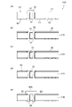
図1(a)~(e)および図2(a)~(e)は、電子機器の組み立て工程を説明する断面図である。図1(a)には、部品が実装される前のプリント基板10が示される。プリント基板10の第1面(先行実装面)S1および第2面S2(後行実装面)には、プリント配線(不図示)や、パッド(ランド)12,14が形成されている。パッド12,14は、部品の電極と対応する箇所に配置され、パッド12,14以外の部分は、レジスト11によって覆われている。
1(a) to (e) and FIGS. 2(a) to (e) are cross-sectional views for explaining the assembly process of the electronic device. FIG. 1(a) shows a printed
図1(b)に示すように、第1面S1の上に、スクリーン(メタルマスクあるいは半田マスクとも称する)20が載置される。スクリーン20には、第1面S1側のパッド12とオーバーラップする箇所に開口22が設けられる。続いて図1(c)に示すように、スクリーン20の上からクリーム半田(半田ペースト)30が塗布される。図1(d)に示すようにスクリーン20を取り外すと、パッド12の上にのみクリーム半田32が残留する。
As shown in FIG. 1B, a screen (also called a metal mask or solder mask) 20 is placed on the first surface S1. The
続いて図1(e)に示すように、マウンタによって第1面S1に部品40がマウントされる。部品40の電極E1,E2と、パッド12の間には、クリーム半田32が挟まれている。この状態でリフロー処理が行われ、部品40と基板10とが電気的、機械的に接続される。
Subsequently, as shown in FIG. 1(e), the
続いて、第2面S2への部品実装を説明する。図2(a)に示すようにプリント基板10は、第2面S2が上側となるように反転される。続いて図2(b)に示すように第2面S2の上にスクリーン50が載置される。スクリーン50には、第2面S2側のパッド14とオーバーラップする箇所に開口52が設けられる。続いて図2(c)に示すように、スクリーン50の上からクリーム半田60が塗布される。図2(d)に示すようにスクリーン50を取り外すと、パッド14の上にのみクリーム半田62が残留する。
Next, component mounting on the second surface S2 will be described. As shown in FIG. 2A, the printed
続いて図2(e)に示すように、マウンタによって第2面S2に部品70がマウントされる。部品70の電極E1,E2と、パッド14の間には、クリーム半田62が挟まれている。この状態でリフロー処理が行われ、部品70と基板10とが電気的、機械的に接続される。以上が表面実装の説明である。
Subsequently, as shown in FIG. 2(e), the
本発明者は表面実装について検討した結果、以下の課題を認識するに至った。プリント基板10は、複数の配線層を含み、異なる配線層の間はビアを介して接続される。ビアは、通常、パッドの位置を避けて配置されるが、放熱性を高めたり、寄生インピーダンスを削減したい場合には、パッド内に配置される場合もある。パッド内に配置されるビアを、パッド内ビアと称する。
As a result of studying surface mounting, the inventor has come to recognize the following problems. The printed
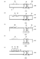
従来の表面実装では、先行実装面である第1面S1にパッド内ビアを形成することが困難であった。図3(a)~(e)は、第1面S1への部品実装を説明する図であり、図4(a)~(e)は、第2面S2への部品実装を説明する図である。 In conventional surface mounting, it is difficult to form intra-pad vias on the first surface S1, which is the preceding mounting surface. FIGS. 3A to 3E are diagrams for explaining component mounting on the first surface S1, and FIGS. 4A to 4E are diagrams for explaining component mounting on the second surface S2. be.
図3(a)には、部品が実装される前のプリント基板10Aが示される。プリント基板10Aの第1面(先行実装面)S1には、パッド(ランド)16およびパッド内ビア17が形成される。
FIG. 3A shows the printed
第1面S1の上にスクリーン20が載置され(図3(b))、続いてスクリーン20の上からクリーム半田30が塗布される(図3(c))。そしてスクリーン20を取り外すと、パッド16の上にクリーム半田32が残留する(図3(d))。
A
続いて、マウンタによって第1面S1に部品40Aがマウントされる(図3(e))。部品40Aは裏面電極E3を有し、裏面電極E3とパッド16の間には、クリーム半田32が挟まれている。この状態でリフロー処理が行われ、部品40Aと基板10とが電気的、機械的に接続される。この工程においてクリーム半田32の一部は、パッド内ビア17(スルーホール)を貫通し、第2面S2側から漏れ出る。この半田の漏れ34は、以下で説明するように実装不良を引き起こす。
Subsequently, the
図4(a)~(e)を参照して第2面S2への部品実装を説明する。図4(a)に示すようにプリント基板10Aは、第2面S2が上側となるように反転される。続いて図4(b)に示すように第2面S2の上にスクリーン50が載置される。スクリーン50は、パッド14とオーバーラップする箇所に開口52を有する。
The mounting of components on the second surface S2 will be described with reference to FIGS. As shown in FIG. 4A, the printed
そして図4(c)に示すようにスクリーン50の上からクリーム半田60が塗布される。図4(d)は、スクリーン50を取り外した状態を示す。クリーム半田62は、パッド14以外の意図しない領域に塗布されている。この状態で第2面S2に部品70をマウントし、リフロー処理にかけると、隣接するパッド14同士がクリーム半田62によってショートするなどの不良が生ずるおそれがある。
Then,
以上が従来の表面実装の問題点である。先行実装面にパッド内ビアを形成したい場合、第2面の実装に、スクリーン印刷を用いず、ニードルディスペンサによって、パッド14の上に選択的にクリーム半田を塗布する方法が考えられる。この方法によれば、第1面S1へのクリーム半田30の影響を受けずに、第2面S2に部品を実装できる。しかしながら、ニードルディスペンサを用いたクリーム半田の塗布は、スクリーン印刷によるそれに比べてスループットが大幅に低下するため、第2面S2の部品点数が多い場合には採用できない。
These are the problems of conventional surface mounting. When it is desired to form intra-pad vias on the preceding mounting surface, a method of selectively applying cream solder onto the
別のアプローチとして、プリント基板10Aの製造工程において、予めビアホールの内部を金属あるいは樹脂で充填して穴を塞ぐという対策が考えられる。この対策によれば、図3(e)の工程において、第2面S2側へのクリーム半田30の漏れを防止できる。しかしながらこの解決方法では、プリント基板10Aの製造工程が増えるため、プリント基板10Aのコストが高くなる。
As another approach, in the manufacturing process of the printed
本発明は係る課題に鑑みてなされたものであり、そのある態様の例示的な目的のひとつは、パッド内ビアに起因する問題を解決可能な表面実装技術の提供にある。 The present invention has been made in view of such problems, and one exemplary purpose of certain aspects thereof is to provide a surface mounting technique capable of solving problems caused by vias in pads.
本発明のある態様は、半導体装置の製造方法に関する。製造方法は、プリント基板の第1面に第1部品群を実装する第1ステップと、プリント基板の第2面に第2部品群を実装する第2ステップと、を備える。プリント基板はパッド内ビアを有する。第1ステップは、第1面の複数のパッドにクリーム半田を塗布するステップと、第1面に第1部品群にマウントするステップと、プリント基板を加熱、冷却するステップと、を含む。第2ステップは、第2面の複数のパッドの箇所に開口を有し、かつパッド内ビアとオーバーラップする箇所に凹部を有するスクリーン(メタルマスク)を、第2面に載せるステップと、スクリーンの上からクリーム半田を塗布し、スクリーンを外すステップと、第2面に第2部品群をマウントするステップと、プリント基板を過熱、冷却するステップと、を備える。 One aspect of the present invention relates to a method for manufacturing a semiconductor device. The manufacturing method includes a first step of mounting a first component group on a first surface of a printed circuit board, and a second step of mounting a second component group on a second surface of the printed circuit board. The printed circuit board has via-in-pad. The first step includes applying cream solder to a plurality of pads on the first surface, mounting a first component group on the first surface, and heating and cooling the printed circuit board. The second step includes placing a screen (metal mask) on the second surface, the screen having openings at the locations of the plurality of pads on the second surface and concave portions at locations overlapping the vias in the pads; It comprises the steps of applying cream solder from above and removing the screen, mounting the second component group on the second surface, and heating and cooling the printed circuit board.
本発明の別の態様は、スクリーンである。このスクリーンは、パッド内ビアを有するプリント基板に部品を実装する際に使用されるスクリーンであって、プリント基板に形成される複数のパッドと対応する箇所に設けられた複数の開口と、パッド内ビアとオーバーラップする箇所に設けられた凹部と、を備える。 Another aspect of the invention is a screen. This screen is used when components are mounted on a printed circuit board having intra-pad vias, and comprises a plurality of openings provided at locations corresponding to a plurality of pads formed on the printed circuit board, and and a recess provided at a location that overlaps with the via.
本発明のさらに別の態様は、電圧安定化モジュールを有する半導体装置の製造方法に関する。製造方法は、プリント基板の第1面に、パワートランジスタを含む第1部品群を実装する第1ステップと、プリント基板の第2面に、インダクタを含む第2部品群を実装する第2ステップと、を備える。プリント基板は、パワートランジスタの裏面電極とオーバーラップする箇所に設けられたパッド内ビアを有する。第1ステップは、第1面の複数のパッドにクリーム半田を塗布するステップと、第1面に第1部品群にマウントするステップと、プリント基板を加熱、冷却するステップと、を含む。第2ステップは、第2面の複数のパッドの箇所に開口を有し、かつパッド内ビアとオーバーラップする箇所に凹部を有するスクリーンを、第2面に載せるステップと、スクリーンの上からクリーム半田を塗布し、スクリーンを外すステップと、第2面に第2部品群をマウントするステップと、プリント基板を過熱、冷却するステップと、を備える。 Yet another aspect of the present invention relates to a method of manufacturing a semiconductor device having a voltage stabilization module. A manufacturing method includes a first step of mounting a first component group including a power transistor on a first surface of a printed circuit board, and a second step of mounting a second component group including an inductor on a second surface of the printed circuit board. , provided. The printed circuit board has intra-pad vias that overlap the backside electrodes of the power transistors. The first step includes applying cream solder to a plurality of pads on the first surface, mounting a first component group on the first surface, and heating and cooling the printed circuit board. The second step includes placing a screen having openings at the locations of the pads on the second surface and concave portions at locations overlapping the vias in the pads on the second surface; and removing the screen; mounting a second group of components on the second surface; and heating and cooling the printed circuit board.
なお、以上の構成要素の任意の組合せ、本発明の表現を、方法、装置、システムなどの間で変換したものもまた、本発明の態様として有効である。 It should be noted that any combination of the above-described components and expressions of the present invention converted between methods, devices, systems, etc. are also effective as aspects of the present invention.
本発明によれば、パッド内ビアに起因する問題を解決できる。 According to the present invention, the problem caused by via-in-pad can be solved.
以下、本発明を好適な実施の形態をもとに図面を参照しながら説明する。各図面に示される同一または同等の構成要素、部材、処理には、同一の符号を付するものとし、適宜重複した説明は省略する。また、実施の形態は、発明を限定するものではなく例示であって、実施の形態に記述されるすべての特徴やその組み合わせは、必ずしも発明の本質的なものであるとは限らない。 BEST MODE FOR CARRYING OUT THE INVENTION The present invention will be described below based on preferred embodiments with reference to the drawings. The same or equivalent constituent elements, members, and processes shown in each drawing are denoted by the same reference numerals, and duplication of description will be omitted as appropriate. Moreover, the embodiments are illustrative rather than limiting the invention, and not all features and combinations thereof described in the embodiments are necessarily essential to the invention.
また図面に記載される各部材の寸法(厚み、長さ、幅など)は、理解の容易化のために適宜、拡大縮小されている場合がある。さらには複数の部材の寸法は、必ずしもそれらの大小関係を表しているとは限らず、図面上で、ある部材Aが、別の部材Bよりも厚く描かれていても、部材Aが部材Bよりも薄いこともあり得る。 Also, the dimensions (thickness, length, width, etc.) of each member shown in the drawings may be appropriately scaled for easier understanding. Furthermore, the dimensions of a plurality of members do not necessarily represent their size relationship. It can be thinner than
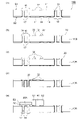
図5(a)~(e)および図6(a)~(e)は、実施の形態に係る電子機器の製造方法を説明する図である。図5(a)~(e)および図6(a)~(e)には、表面実装による組み立て工程が示される。 FIGS. 5A to 5E and 6A to 6E are diagrams for explaining the method of manufacturing the electronic device according to the embodiment. FIGS. 5(a)-(e) and FIGS. 6(a)-(e) show assembly steps by surface mounting.
図5(a)~(e)を参照して、第1面S1への部品実装を説明する。第1面S1への実装については、以下で説明するように図3と実質的に同様である。 Component mounting on the first surface S1 will be described with reference to FIGS. Mounting on the first surface S1 is substantially the same as in FIG. 3, as described below.
図5(a)には、部品が実装される前のプリント基板10Bが示される。プリント基板10Bの第1面(先行実装面)S1には、いくつかのパッド(ランド)12,16が形成される。パッド16には、パッド内ビア17が形成される。プリント基板10B第2面(後行実装面)S2にも同様に、いくつかのパッド14,18が形成される。パッド18には、パッド内ビア19が形成される。
FIG. 5(a) shows the printed
図5(b)に示すように、第1面S1の上にスクリーン20が載置される。スクリーン20には、パッド12,16に対応する箇所に、開口22,24が設けられる。続いてスクリーン20の上からクリーム半田30が塗布される(図5(c))。
As shown in FIG. 5B, the
そしてスクリーン20を取り外すと、パッド12,16の上にクリーム半田32が残留する(図5(d))。
When the
続いて、マウンタによって第1面S1に部品40,40Aがマウントされる(図5(e))。部品40の電極E1,E2と、パッド12の間には、クリーム半田32が挟まれている。部品40Aは裏面電極E3を有し、裏面電極E3とパッド16の間には、クリーム半田32が挟まれている。この状態でリフロー処理が行われ、部品40Aと基板10とが電気的、機械的に接続される。
Subsequently, the
この工程においてクリーム半田32の一部は、パッド内ビア17(スルーホール)を貫通し、第2面S2側から漏れ出る。
In this process, part of the
続いて図6(a)~(e)を参照して第2面S2への部品実装を説明する。図6(a)に示すようにプリント基板10Bは、第2面S2が上側となるように反転される。続いて図6(b)に示すように、第2面S2の上に、スクリーン50Bが載置される。
Next, component mounting on the second surface S2 will be described with reference to FIGS. 6(a) to 6(e). As shown in FIG. 6A, the printed
本実施の形態において、スクリーン50Bは、パッド14とオーバーラップする箇所に開口52を有する。それに加えてスクリーン50Bには、パッド内ビア19とオーバーラップする箇所に、凹部56が設けられている。この凹部56によって、スクリーン50Bが半田の漏れ34と干渉しないようになっており、スクリーン50Bを第2面S2に密着させることが可能となる。
In this embodiment, the
図6(d)は、スクリーン50Bを取り外した状態を示す。クリーム半田62は、パッド14、18の上にのみ塗布されており、余計なはみ出しが抑えられている。
FIG. 6(d) shows a state in which the
続いて図6(e)のように、第2面S2に部品70,70Aがマウントされ、リフロー処理にかけられる。これにより部品70に関して、電極E1,E2がパッド14と電気的、機械的に接続される。また部品70Aに関しても、裏面電極E3とパッド18とが電気的、機械的に接続され、半導体装置100が組み立てられる。
Subsequently, as shown in FIG. 6(e), the
以上が実施の形態に係る半導体装置の製造方法である。 The above is the manufacturing method of the semiconductor device according to the embodiment.
このように、本実施の形態によれば、第2面S2にクリーム半田を塗布する際に用いるスクリーン50に、半田の漏れ34との干渉を避けるための凹部56を設けることとした。これにより、半田の漏れ34によるスクリーン50Bの位置ズレを防止でき、またスクリーン50Bと第2面S2の間のギャップにクリーム半田60が侵入するのを防止できる。
As described above, according to the present embodiment, the
なお第2面S2に部品70Aを実装する際に、パッド内ビア19から第1面S1側にも、半田の漏れ64が生じうるが、第1面S1側の部品の実装は完了しているため、悪影響はない。
When the
続いて、実施の形態に係る製造方法の用途を説明する。実施の形態に係る製造方法は、以下で説明するDC/DCコンバータの製造工程に利用可能であり、上述の第1面S1に実装される部品40Aは、第1面S1に実装される後述のパワーモジュール220に対応付けられる。
Next, applications of the manufacturing method according to the embodiment will be described. The manufacturing method according to the embodiment can be used in the manufacturing process of the DC/DC converter described below. It is associated with
パーソナルコンピュータやゲーム専用機などの電子機器において、電池、あるいはインバータから供給される直流電圧を、負荷に最適な電圧レベルに降圧するDC/DCコンバータ(スイッチングレギュレータ)が利用される。 2. Description of the Related Art Electronic devices such as personal computers and dedicated game machines use a DC/DC converter (switching regulator) that steps down a DC voltage supplied from a battery or an inverter to a voltage level that is optimal for a load.
図7は、マルチフェーズの降圧DC/DCコンバータの構成例を示す回路図である。DC/DCコンバータ200は、Nフェーズ(N≧2)で構成され、入力ライン202、出力ライン204、N個のインダクタL1_1~L1_N、入力キャパシタCi、出力キャパシタCo、コントローラ210、N個のパワーモジュール220_1~220_Nを備える。
FIG. 7 is a circuit diagram showing a configuration example of a multiphase step-down DC/DC converter. The DC/
出力ライン204には、消費電力(負荷電流IOUT)がダイナミックに変化する負荷(不図示)が接続される。DC/DCコンバータ200は、入力ライン202の入力電圧VINを受け、所定レベルに安定化された出力電圧VOUTを生成し、負荷に供給する。入力ライン202には、入力電圧VINを安定化させるための入力キャパシタCiが接続され、出力ライン204には、出力電圧VOUTを平滑化するための出力キャパシタCoが接続される。
A load (not shown) whose power consumption (load current I OUT ) dynamically changes is connected to the
パワーモジュール220は、主として、VINピン、PGNDピン、SWピン、VCCピン、AGNDピン、PWMピンを備える。パワーモジュール220は、VINピンとSWピンの間に設けられたハイサイドスイッチ(スイッチングトランジスタ)M1と、SWピンとPGNDピンの間に設けられたローサイドスイッチ(同期整流トランジスタトランジスタ)M2と、ハイサイドドライバ222、ローサイドドライバ224、ロジック回路226を含む。
The
コントローラ210は、複数のインダクタL1_1~L1_Nそれぞれに流れる電流あるいは負荷電流IOUTを監視し、駆動フェーズ数Kを決定する。たとえばN=4の場合、Kは、1,2,3,4の4つの値(あるいは1,2,4の3つの値)から選択可能とされる。
The
またコントローラ210は、出力電圧VOUTに応じたフィードバック信号VFBを受け、フィードバック信号VFBが所定の目標電圧VREFに近づくように、デューティ比が調節されるパルス信号SPWMを生成し、N個のパワーモジュール220_1~220_Nのうち、K個に分配する。K個のパワーモジュール220_1~220_Kには、(360/K)度の位相差を有するパルス信号SPWM1~SPWMKが分配される。
Further, the
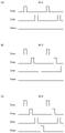
以上がDC/DCコンバータ200の構成である。続いてその動作を説明する。ここではM=4であり、駆動フェーズ数Kは2、3、4を取りうる場合を説明する。図8(a)~(c)はそれぞれ、K=2、3、4のときのスイッチング電圧Vsw1~Vsw4を示す波形図である。
The above is the configuration of the DC/
DC/DCコンバータ200の構成部品はプリント基板上に実装される。従来のDC/DCコンバータ200は、主要な構成部品であるインダクタL1_1~L1_N、パワーモジュール220_1~220_Nが、同一実装面にマウントされていた。ここでいう主要な構成部品とは、専有面積が大きく、また大電流が流れる部品である。
Components of the DC/
主要な構成部品を同一実装面に実装すると、DC/DCコンバータ200の専有面積が大きくなる。これはプリント基板の面積が大きくなることを意味し、コストアップの一因となり得る。
Mounting the main components on the same mounting surface increases the area occupied by DC/
また、複数のパワーモジュール220_1~220_Nの発熱が大きいアプリケーションでは、複数のパワーモジュール220_1~220_Nをヒートシンクで冷却する必要がある。ところが複数のパワーモジュール220_1~220_Nが、複数のインダクタL1_1~L1_Nなどの他の部品と近接配置すると、ヒートシンクの形状が、他の部品によって制約され、冷却効果が犠牲になるおそれがある。 Also, in applications where the power modules 220_1 to 220_N generate a large amount of heat, it is necessary to cool the power modules 220_1 to 220_N with heat sinks. However, if the plurality of power modules 220_1-220_N are arranged close to other components such as the plurality of inductors L1_1-L1_N, the shape of the heat sink may be restricted by the other components, and the cooling effect may be sacrificed.
反対に、冷却効果を優先してレイアウトを決めると、パワーモジュールとインダクタの距離が遠くなり、DC/DCコンバータ200の専有面積が大きくなり、コストアップの要因となりうる。
Conversely, if the layout is determined with priority given to the cooling effect, the distance between the power module and the inductor increases, and the area occupied by the DC/
(第1の実施の形態)
本発明の一側面は、DC/DCコンバータのレイアウトあるいは実装技術として把握される。本実施の形態において、DC/DCコンバータの機能あるいは等価回路については、図7と同様である。
(First embodiment)
One aspect of the present invention is grasped as a layout or mounting technology of a DC/DC converter. In this embodiment, the function or equivalent circuit of the DC/DC converter is the same as in FIG.
いくつかの実施例で共通となるパワーモジュール220について説明する。パワーモジュール220自体は、公知であり、さまざまなICメーカによって製造・販売されている。
A
パワーモジュール220の回路構成は、図7と同様であり、ハイサイドトランジスタM1、ローサイドトランジスタM2、ハイサイドドライバ222、ローサイドドライバ224、ロジック回路226を備える。またパワーモジュール220は、入力(VIN)ピン、スイッチングピン(SW)、グランドピン(PGND,AGND)、電源(VCC)ピン、制御(PWM)ピンなどを備える。なお、パワーモジュール220は、ブートストラップ回路や、各種保護回路などを備え、またそれらに関連する複数のピンを備えるが、本発明と無関係であるため図示せず、説明を省略する。
The circuit configuration of the
ロジック回路226をはじめとする各回路ブロックには、VCCピンを介して電源電圧VCCが供給される。AGNDピンは、ハイサイドドライバ222、ローサイドドライバ224、ロジック回路226等のグランドである。VINピンには、直流の入力電圧VINが供給され、PGNDピンは、出力段のグランドである。
Each circuit block including the logic circuit 226 is supplied with the power supply voltage VCC through the VCC pin. The AGND pin is the ground for
ロジック回路226は、PWMピンに入力されるPWM信号SPWMに応じて、ハイサイドパルス、ローサイドパルスを生成する。ハイサイドドライバ222はハイサイドパルスにもとづいてハイサイドトランジスタM1を駆動し、ローサイドドライバ224は、ローサイドパルスにもとづいてローサイドトランジスタM2を駆動する。
The logic circuit 226 generates a high side pulse and a low side pulse according to the PWM signal S PWM input to the PWM pin. The
続いて主要な回路部品のパッケージのピン配置を説明する。図9(a)は、パワーモジュール220の裏面電極のレイアウト図である。上述のようパワーモジュール220は、VINピン、PGNDピン、SWピン、VCCピン、AGNDピンを備える。この中で、VINピンとGNDピンは、相対的に他のパッドよりも面積が大きい。特にPGNDピン、AGNDピンはサーマルパッドとしての機能も有するため、面積が大きい。PWMピンやその他の制御ピンは、残りのピンに割り当てられる。なお、図9の裏面電極のレイアウトは例示に過ぎず、チップベンダーや製品ごとに異なることは言うまでもない。
Next, the pin arrangement of the package of the main circuit parts will be explained. FIG. 9A is a layout diagram of the back electrode of the
図9(b)は、インダクタL1の裏面電極のレイアウト図である。インダクタL1は、対向する2辺の中央に配置された第1電極E1と第2電極E2を有する。 FIG. 9B is a layout diagram of the back electrode of the inductor L1. The inductor L1 has a first electrode E1 and a second electrode E2 arranged in the center of two opposing sides.
本実施の形態において解決しようとする課題のひとつは、レイアウトの改善である。そこではじめに、比較の基準となるレイアウト(以下、比較技術という)について説明する。 One of the problems to be solved in this embodiment is layout improvement. Therefore, first, a layout that serves as a reference for comparison (hereinafter referred to as a comparison technique) will be described.
近年の電子回路は、表面実装技術(SDT:Surface Mount Technology)を用いて実装される。表面実装では、プリント基板上に形成されたパッド(ランド)に、クリーム半田を塗布し、マウンタを用いて部品を実装し、リフロー処理を行う。 Electronic circuits in recent years are mounted using surface mount technology (SDT). In surface mounting, cream solder is applied to pads (lands) formed on a printed circuit board, components are mounted using a mounter, and reflow processing is performed.
プリント基板の両面に表面実装により部品を実装する場合、一方の面(先行実装面)に部品を実装する。続いて、プリント基板を裏返した後に、他方の面(後行実装面)に部品を実装する。後行実装面をリフロー処理すると、先行実装面の半田が再加熱される。先行実装面に実装済みの部品が重かったり大きかったりすると、実装済みの部品が位置ズレを起こしたり、落下するおそれがある。この理由から、先行実装面に実装できる部品には、大きさや重さに制約があり、したがって先行実装面が副実装面となるのが一般的である。つまり副実装面には、相対的に少ない部品、軽い部品、小さい部品が実装され、主実装面には、相対的に多くの部品、重い部品、大きな部品が実装される。DC/DCコンバータについても例外ではなく、よって比較技術においても基本的にはすべての部品が主実装面に実装される。 When mounting components on both sides of a printed circuit board by surface mounting, the components are mounted on one surface (preceding mounting surface). Subsequently, after turning over the printed circuit board, components are mounted on the other surface (subsequent mounting surface). When the subsequent mounting surface is reflowed, the solder on the preceding mounting surface is reheated. If the parts already mounted on the preceding mounting surface are heavy or large, the already mounted parts may be misaligned or dropped. For this reason, there are restrictions on the size and weight of components that can be mounted on the preceding mounting surface, so the preceding mounting surface is generally the secondary mounting surface. That is, relatively few parts, light parts, and small parts are mounted on the sub-mounting surface, and relatively many parts, heavy parts, and large parts are mounted on the main mounting surface. DC/DC converters are no exception, and therefore basically all components are mounted on the main mounting surface in the comparative technology as well.
図10は、比較技術に係るDC/DCコンバータのレイアウト図である。この例では、N=3とする。コントローラ210、パワーモジュール220_1~220_N、入力キャパシタCi、出力キャパシタCo(主要構成部品という)はすべて、プリント基板300Rの主実装面SAにレイアウトされている。
FIG. 10 is a layout diagram of a DC/DC converter according to a comparative technique. In this example, N=3.
複数のインダクタL1_1~L1_Nは、プリント基板上の第1方向(x方向)に並べて配置される。パワーモジュール220_#(#=1,2…N)は、対応するインダクタL1_#と第2方向(y方向)に隣接して配置される。これによりパワーモジュール220_#とインダクタL1_#の間の寄生抵抗を下げることができる。 A plurality of inductors L1_1 to L1_N are arranged side by side in the first direction (x direction) on the printed circuit board. The power modules 220_# (#=1, 2 . . . N) are arranged adjacent to the corresponding inductors L1_# in the second direction (y-direction). This can reduce the parasitic resistance between power module 220_# and inductor L1_#.
図11は、比較技術に係るプリント基板300Rの配線パターンを示す図である。図中、丸で示すのはビアホールである。プリント基板300には、複数のパターン配線(プリント配線)PTN1_1~PTN1_3,PTN_2,PTN3_1~PTN3_3,PTN4が形成される。第1パターン配線PTN1_1~PTN1_3は、図7の入力ライン202_1~202_3に対応している。パワーモジュール220_#(#=1,2…N)の入力ピンVINは、対応する第1パターン配線PTN1_#のパッドと接続される。
FIG. 11 is a diagram showing a wiring pattern of a printed
第2パターン配線PTN2は、グランドプレーンであり、インピーダンスを極力小さくするために、全フェーズ共通で形成されている。パワーモジュール220_#(#=1,2…N)の接地ピンPGNDは、対応するパターン配線PTN2のパッドと接続される。 The second pattern wiring PTN2 is a ground plane, and is formed in common for all phases in order to minimize impedance. The ground pins PGND of the power modules 220_# (#=1, 2, . . . N) are connected to pads of the corresponding pattern wiring PTN2.
第1パターン配線PTN1_#と第2パターン配線PTN2の間には、入力キャパシタCi_#が設けられる。入力キャパシタCi_#は、MLCC(多層セラミックコンデンサ)や電解コンデンサであり、あるいはそれらの組み合わせでありうる。 An input capacitor Ci_# is provided between the first pattern wiring PTN1_# and the second pattern wiring PTN2. The input capacitor Ci_# can be an MLCC (multilayer ceramic capacitor), an electrolytic capacitor, or a combination thereof.
第3パターン配線PTN3_1~PTN3_3は、図7においてパワーモジュール220のSWピンとインダクタL1の一端を結ぶ配線である。パワーモジュール220_#(#=1,2…N)のSWピンSWは、対応する第3パターン配線PTN3_#のパッドと接続される。またインダクタL1_#(#=1,2…N)の電極E1は、対応する第3パターン配線PTN3_#のパッドと接続される。
The third pattern wirings PTN3_1 to PTN3_3 are wirings that connect the SW pins of the
第4パターン配線PTN4は、図7における出力ライン204に対応する。インダクタL1_#(#=1,2…N)の電極E2は、対応する第4パターン配線PTN4のパッドと接続される。第4パターン配線PTN4とグランドプレーンの間には、図7の出力キャパシタCo(図11において不図示)が接続される。
The fourth pattern wiring PTN4 corresponds to the
第1パターン配線PTN1~第4パターン配線PTN4は、大電流が流れるため、インピーダンスをなるべく小さくする必要がある。したがってこれらのパターン配線PTN1~PTN4はそれぞれが多層配線を形成しており、図11に図示しない別の配線層の配線と、ビアホールを介して接続されている。 Since a large current flows through the first pattern wiring PTN1 to the fourth pattern wiring PTN4, it is necessary to reduce the impedance as much as possible. Therefore, these pattern wirings PTN1 to PTN4 each form a multilayer wiring, and are connected to wirings of another wiring layer (not shown in FIG. 11) through via holes.
以上が比較技術に係る部品レイアウトである。続いて、実施の形態に係るレイアウトを説明する。本実施の形態では、N個のパワーモジュール220の少なくともひとつをプリント基板300の主実装面SAと反対側の副実装面SBに実装することとした。以下、いくつかの実施例を説明する。
The above is the component layout according to the comparative technique. Next, a layout according to the embodiment will be described. In this embodiment, at least one of the
(実施例1-1)
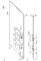
図12(a)、(b)は、実施例1-1に係るDC/DCコンバータ200Aのレイアウト図である。図12(a)は斜視図を、図12(b)は断面図を示す。実施例1-1では、すべてのパワーモジュール220_1~220_3が、副実装面SBに実装されている。入力キャパシタCi_#は、パワーモジュール220_#のVINピンの直近に接続することが好ましい。そこで実施例1-1では、入力キャパシタCi_#も副実装面SBに実装される。
(Example 1-1)
12A and 12B are layout diagrams of a DC/
図13は、実施例1-1に係るDC/DCコンバータ200Aの配線パターンを示す図である。図13において、主実装面SA側に実装される部品は破線で示し、副実装面SB側に実装される部品は二点鎖線で示す。パターン配線PTN1~PTN4の機能は、図11と同様である。またパターン配線PTN1~PTN4は多層配線であり、主実装面SA、副実装面SBの両面(および中間の配線層)にオーバーラップして形成され、それらは互いにビアホールで電気的に接続されている。
FIG. 13 is a diagram showing a wiring pattern of the DC/
以上が実施例1-1に係るDC/DCコンバータ200Aの構成である。副実装面SBをパワーモジュール220の実装に利用することで、主実装面SAあるいは副実装面SBにスペース的な余裕が生ずる。このことによる利点を説明する。
The above is the configuration of the DC/
図14は、DC/DCコンバータ200Aを副実装面SB側からみた斜視図である。DC/DCコンバータ200Aは、ヒートシンク240を備える。ヒートシンク240は、複数のパワーモジュール220_1~220_3それぞれの上面と共通して接している。副実装面SB側には、パワーモジュール220_1~220_Nの周囲に、パワーモジュール220より背の高い部品は存在しないため、大きなヒートシンク240を設けることができ、冷却効率を高めることができる。
FIG. 14 is a perspective view of the DC/
ヒートシンクの具体的な構成例を説明する。図15(a)、(b)は、第1構成例に係るヒートシンク240Aの断面図である。図15(a)は、実施例1-1にヒートシンク240Aを適用した様子を示し、図15(b)は、図10の比較技術に同じヒートシンク240Aを適用した様子を示す。
A specific configuration example of the heat sink will be described. 15A and 15B are cross-sectional views of a
ヒートシンク240Aは、放熱部分242とコンタクト部分244を有する。放熱部分242には開口が設けられており、この開口にコンタクト部分244が嵌め込まれている。コンタクト部分244は、冷却対象のパワーモジュール220と接触する。
The
実施例1-1と比較技術を対比する。図15(b)に示すように、パワーモジュール220が主実装面SAに実装される比較技術では、パワーモジュール220の周辺に、背の高い部品221(たとえばインダクタ)が存在する。したがって放熱部分242をプリント基板表面に近づけることが難しくなり、コンタクト部分244のZ方向の高さが高くなる。これは熱抵抗の増加の要因となり、すなわち冷却性能の低下を意味する。
The comparative technique is contrasted with Example 1-1. As shown in FIG. 15(b), in the comparative technique in which the
これに対してパワーモジュール220が副実装面SBに実装される実施例1-1では、図15(a)に示すように、パワーモジュール220の周辺に、背の高い部品が存在しないため、放熱部分242をプリント基板表面に近づけることができる。これにより、コンタクト部分244のZ方向の高さを低くできる。これにより熱抵抗を下げ、冷却性能の改善できる。
On the other hand, in embodiment 1-1 in which the
図16(a)、(b)は、第2構成例に係るヒートシンク240Bの断面図である。ヒートシンク240Bは、一枚の放熱板246で構成され、絞り加工により凸部248が設けられ、放熱板246は凸部248において、パワーモジュール220の表面と接触する。
16A and 16B are cross-sectional views of a
実施例1-1と比較技術を対比する。図16(b)に示すように比較技術では、パワーモジュール220の周辺に、背の高い部品221(たとえばインダクタ)が存在する。凸部248が部品221と干渉するため、比較技術では、第2構成例を採用することが難しい。
The comparative technique is contrasted with Example 1-1. As shown in FIG. 16(b), in the comparative technique, a tall component 221 (for example, an inductor) exists around the
これに対してパワーモジュール220が副実装面SBに実装される実施例1-1では、パワーモジュール220の周辺に、ヒートシンク240Bの凸部248と干渉する部品が存在しない。したがって、ヒートシンク240Bの設計の自由度が高まり、第2構成例に係るヒートシンク240Bを採用できる。
On the other hand, in Example 1-1 in which the
図16のヒートシンク240Bは、図15のヒートシンク240Aと比較して構造が簡素化されているため、コストを下げることができる。また開口が不要であることから、電磁ノイズの遮蔽性能が高く、EMC(Electro Magnetic Compatibility)を改善できる。
Since the
(実施例1-2)
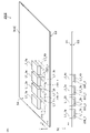
実施例1-2では、N=4のDC/DCコンバータ200Bについて説明する。図17(a)、(b)は、実施例1-2に係るDC/DCコンバータ200Bのレイアウト図である。図17(a)は斜視図を、図17(b)は断面図を示す。実施例1-2では、N個のパワーモジュール220_1~220_Nは、主実装面SAと副実装面SBに交互に実装される。具体的には奇数番目のパワーモジュール220_#(#=1,3,…)は、副実装面SBに実装され、偶数番目のパワーモジュール220_*(*=2,4,…)は、主実装面SAに実装される。もちろん逆であってもよい。
(Example 1-2)
In Example 1-2, a DC/
図18は、実施例1-2に係るDC/DCコンバータ200Bの配線パターンを示す図である。図18において、主実装面SA側に実装される部品は破線で示し、副実装面SB側に実装される部品は二点鎖線で示す。パターン配線PTN1~PTN4の機能は、上述した通りである。またパターン配線PTN1~PTN4は多層配線であり、主実装面SA、副実装面SBの両面(および中間の配線層)にオーバーラップして形成され、それらは互いにビアホールで電気的に接続されている。
FIG. 18 is a diagram showing a wiring pattern of a DC/
実施例1-2において、N個のパワーモジュールは、1番目と2番目、3番目と4番目、…とペアをなしている。そしてペアをなす2個のパワーモジュール220_i,220_jは、共通の入力ライン(すなわち共通の第1パターン配線PTN1_i,j)と接続される。 In Example 1-2, the N power modules are paired first and second, third and fourth, and so on. Two power modules 220_i and 220_j forming a pair are connected to a common input line (that is, common first pattern wiring PTN1_i, j).
実施例1-1あるいは比較技術のように、すべてのパワーモジュール220を同一実装面に実装すると、パワーモジュール220ごとに、第1パターン配線PTN1を形成する必要がある。これに対して、実施例1-2のように、主実装面SAと副実装面SBに交互にパワーモジュール220を実装することで、VIN端子同士が隣接することになるため、入力ラインを共通化できるという利点がある。
When all the
加えて、入力ライン(第1パターン配線PTN1_i,j)が共通化されると、入力キャパシタCi_i,jも共通化できるという利点がある。すなわち、主実装面SA側の入力キャパシタCi_i,jは、パワーモジュール220_iの入力キャパシタとして機能すると同時に、副実装面SB側のパワーモジュール220_jの入力キャパシタとしても機能するため、入力キャパシタの効果を倍増することができる。あるいは、同じ入力キャパシタの効果を得るために必要なキャパシタの個数を減らすことができ、コストを削減できる。 In addition, if the input line (first pattern wiring PTN1_i,j) is shared, there is an advantage that the input capacitor Ci_i,j can also be shared. That is, the input capacitor Ci_i,j on the side of the main mounting surface SA functions as an input capacitor of the power module 220_i and simultaneously functions as an input capacitor of the power module 220_j on the side of the sub-mounting surface SB, thus doubling the effect of the input capacitor. can do. Alternatively, the number of capacitors required to obtain the same input capacitor effect can be reduced, resulting in cost savings.
(実施例1-3)
図19(a)、(b)は、実施例1-3に係るDC/DCコンバータ200Dのレイアウト図である。実施例1-3は、実施例1-2のインダクタのチップサイズを小さくしたものである。インダクタL1に流れる電流が小さいアプリケーションでは、許容電流が小さい、すなわちチップサイズが小さい部品を選定でき、専有面積を小さくできる。
(Example 1-3)
19A and 19B are layout diagrams of a DC/
(実施例1-4)
図20(a)、(b)は、実施例1-4に係るDC/DCコンバータ200Gのレイアウト図である。実施例1-4は、実施例1-3から、インダクタのレイアウトを変更したものであり、具体的には、各インダクタL1_iは、それと対応するパワーモジュール220_iと同一面に実装される。これにより対応するインダクタL1_iとパワーモジュール220_iを低インピーダンスで接続できる。
(Example 1-4)
20(a) and (b) are layout diagrams of a DC/
より好ましくは、インダクタL1_1とL1_2のペアは、プリント基板300Gの両面SA,SBにオーバーラップして実装される。またインダクタL1_3とL1_4のペアは、プリント基板300Gの両面SA,SBにオーバーラップして実装される。これにより、隣接するインダクタの間隔を大きくすることができ、図19(a)、(b)のレイアウトに比べて熱的な集中を緩和できる。
More preferably, the pair of inductors L1_1 and L1_2 are mounted overlappingly on both surfaces SA and SB of the printed
(第2の実施の形態)
実施例1-3において説明したように、インダクタL1に流れるコイル電流が小さいアプリケーションでは、チップサイズを小さくすることができる。しかしながら、インダクタL1に流れるコイル電流が大きいアプリケーションでは、許容電流が大きな、したがってチップサイズの大きな部品を選定せざるをえず、DC/DCコンバータの占有サイズが、インダクタのチップサイズによって制約を受けることとなる。第2の実施の形態では、コイル電流が大きなアプリケーションにおいて、DC/DCコンバータの占有サイズを小さくする技術を説明する。
(Second embodiment)
As described in Example 1-3, the chip size can be reduced in applications where the coil current flowing through inductor L1 is small. However, in applications where the coil current flowing through the inductor L1 is large, a component with a large allowable current and therefore a large chip size must be selected, and the occupied size of the DC/DC converter is restricted by the chip size of the inductor. becomes. In the second embodiment, a technique for reducing the occupied size of the DC/DC converter in an application with a large coil current will be described.
図21は、第2の実施の形態に係るDC/DCコンバータ200Cの等価回路図である。DC/DCコンバータ200Cにおいて、インダクタL1_#(#=1,2…N)はそれぞれ、インダクタンス値が等しく、チップサイズが同一である2個のインダクタチップL1_#a、L1_#bの並列接続で構成される。
FIG. 21 is an equivalent circuit diagram of a DC/
2並列の場合のインダクタチップのインダクタンス値は、単一のインダクタチップの場合の1/2倍となる。一方、2並列の場合に、インダクタチップに流れる電流量は、単一のインダクタチップの場合の1/2倍となる。第2の実施の形態では、チップ当たりの電流量を減らすことで、電流容量の小さい、したがってパッケージサイズの小さいインダクタチップを選定することができる。たとえば、単一のインダクタチップの場合に10mm角のインダクタチップを採用する場合、第2の実施の形態の技術思想を導入して、2並列とすることにより、6mm角のインダクタチップを採用することができる。 The inductance value of the inductor chip in the case of two parallels is half that in the case of a single inductor chip. On the other hand, in the case of two parallel inductor chips, the amount of current flowing through the inductor chip is half that in the case of a single inductor chip. In the second embodiment, by reducing the amount of current per chip, an inductor chip with a small current capacity and thus a small package size can be selected. For example, when adopting a 10 mm square inductor chip in the case of a single inductor chip, a 6 mm square inductor chip can be adopted by introducing the technical idea of the second embodiment and connecting two in parallel. can be done.
DC/DCコンバータ200を搭載した製品を量産する際には、チップ部品の入手性を考慮する必要がある。特に、長い期間にわたり大量に製造、販売される製品では、チップ部品が長期間にわたり安定的に供給される必要がある。現在、チップ部品の小型化が進められており、小さいサイズのインダクタチップのラインナップが増えている代わりに、大きなサイズのチップ部品の入手性が悪くなっている。この観点において、従来において大きなチップサイズのインダクタを、チップサイズの小さい複数のインダクタチップの並列接続に置換することとで、入手性の問題を解決することができる。
When mass-producing products incorporating the DC/
(実施例2-1)
図22(a)、(b)は、実施例2-1に係るDC/DCコンバータ200Cのレイアウト図である。図22(a)は斜視図を、図22(b)は断面図を示す。
(Example 2-1)
22(a) and (b) are layout diagrams of a DC/
電気的に並列に接続される2個のインダクタチップL1_#a、L1_#bは、プリント基板300Cの主実装面SAと副実装面SBに、互いにオーバーラップして実装される。
The two inductor chips L1_#a and L1_#b electrically connected in parallel are mounted overlapping each other on the main mounting surface SA and the sub-mounting surface SB of the printed
実施例2-1では、N個のパワーモジュール220_1~220_Nは、第1の実施の形態の実施例1-2と同様に、主実装面SAと副実装面SBに交互に実装される。 In Example 2-1, N power modules 220_1 to 220_N are alternately mounted on the main mounting surface SA and the sub-mounting surface SB as in Example 1-2 of the first embodiment.
図23は、実施例2-1に係るDC/DCコンバータ200Cの配線パターンを示す図である。DC/DCコンバータの占有領域のX方向の長さ(全幅)Wは、インダクタチップの横幅wによって支配的に規定され、具体的には、W=w×N+s×(N-1)となる。sは、インダクタチップのx方向の間隔である。たとえば10mm角のインダクタチップを、6mm角のインダクタチップに置き換えたとすれば、N=4の場合で、DC/DCコンバータの占有領域の全幅を、おおよそ4mm×4=16mm程度、小さくすることができる。
FIG. 23 is a diagram showing a wiring pattern of a DC/
加えて実施例2-1によれば、実施例1-2と同じ効果を得ることができる。すなわち、隣接する2フェーズで入力ラインを共通化でき、また入力キャパシタCi_i,jも共通化できる。 In addition, according to Example 2-1, the same effect as Example 1-2 can be obtained. That is, two adjacent phases can share an input line and also share an input capacitor Ci_i,j.
(実施例2-2)
図24(a)、(b)は、実施例2-2に係るDC/DCコンバータ200Eのレイアウト図である。図24(a)は斜視図を、図24(b)は断面図を示す。実施例2-2は、複数のパワーモジュール220_1~220_4が副実装面SBに実装される点において、図12の実施例1-1と共通する。図24では、入力キャパシタCiは省略するが、実施例1-1と同様に、副実装面SBに実装すればよい。
(Example 2-2)
24(a) and (b) are layout diagrams of a DC/DC converter 200E according to Example 2-2. FIG. 24(a) shows a perspective view, and FIG. 24(b) shows a sectional view. Example 2-2 is common to Example 1-1 in FIG. 12 in that a plurality of power modules 220_1 to 220_4 are mounted on sub-mounting surface SB. Although the input capacitor Ci is omitted in FIG. 24, it may be mounted on the sub-mounting surface SB as in the embodiment 1-1.
実施例2-2によれば、実施例2-1と同様に、DC/DCコンバータ200Eの専有面積を小さくできる。 According to the embodiment 2-2, the area occupied by the DC/DC converter 200E can be reduced as in the embodiment 2-1.
(実施例2-3)
図25(a)、(b)は、実施例2-3に係るDC/DCコンバータ200Fのレイアウト図である。図25(a)は斜視図を、図25(b)は断面図を示す。実施例2-3では、複数のパワーモジュール220_1~220_4はすべて主実装面SA側に実装される。
(Example 2-3)
25(a) and (b) are layout diagrams of a DC/
実施例2-3によれば、実施例2-1、実施例2-2と同様に、DC/DCコンバータ200Fの専有面積を小さくできる。
According to the embodiment 2-3, similarly to the embodiments 2-1 and 2-2, the area occupied by the DC/
(変形例2-1)
実施例2-1~2-3において、フェーズごとのインダクタL1を、2個のインダクタチップの並列接続としたが、チップの個数は2に限定されず、3個以上としてもよい。
(Modification 2-1)
In Examples 2-1 to 2-3, the inductor L1 for each phase is a parallel connection of two inductor chips, but the number of chips is not limited to two, and may be three or more.
(実装技術)
続いてパワーモジュール220の実装技術を説明する。
(mounting technology)
Next, a mounting technique for the
図7を参照する。DC/DCコンバータ200において、入力ライン202のインダクタ成分や抵抗成分は極力小さいことが望ましい。またPGNDピンについても、なるべく小さなインピーダンスで接地されることが望ましい。図11や図13に示したように、第1パターン配線PTN1には、VINピンを半田付けするためのパッド(ランド)が形成され、第2パターン配線PTN2には、PGNDピンを半田付けするためのパッド(ランド)が形成される。パターン配線PTN1,PTN2のインピーダンスを下げるために、多層配線が採用され、ビアホールが多数設けられるが、インピーダンスを可能な限り下げるためには、パッド(ランド)の内側に、ビアホールを形成することが要求される。このようなビアホールを、パッド内ビアと称する。
Please refer to FIG. In the DC/
図11の比較技術では、パワーモジュール220が主実装面にのみ実装されるため、パッド内ビアの形成に格別の困難性はない。ところが、実施例1-1,1-2,1-3,2-1,2-2では、パワーモジュール220が副実装面に実装されるため、副実装面にパッド内ビアを形成する必要がある。コストを無視すれば、副実装面にパッド内ビアを形成することは不可能ではないが、コストを考慮した場合、従来の表面実装では、副実装面にパッド内ビアを設けることは容易ではない。実施の形態で説明した実装技術は、パッド内ビアを必要とするパワーモジュール220の実装に好適である。
In the comparative technique of FIG. 11, since the
以上、本発明を実施の形態をもとに説明した。実施の形態は例示であり、それらの各構成要素や各処理プロセスの組合せにいろいろな変形例が可能なこと、またそうした変形例も本発明の範囲にあることは当業者に理解されるところである。 The present invention has been described above based on the embodiments. It should be understood by those skilled in the art that the embodiment is an example, and that various modifications can be made to combinations of each component and each treatment process, and that such modifications are within the scope of the present invention. .
10 プリント基板
12,14,16 パッド
17 パッド内ビア
18 パッド
19 パッド内ビア
S1 第1面
S2 第2面
20 スクリーン
22 開口
30 クリーム半田
32 クリーム半田
34 半田の漏れ
40 部品
E1,E2 電極
E3 裏面電極
50 スクリーン
52,54 開口
56 凹部
60 クリーム半田
70 部品
10 Printed
Claims (4)
プリント基板の第1面に第1部品群を実装する第1ステップと、
前記プリント基板の第2面に第2部品群を実装する第2ステップと、
を備え、
前記プリント基板はパッド内ビアを有し、
前記第1ステップは、
前記第1面の複数のパッドにクリーム半田を塗布するステップと、
前記第1面に前記第1部品群にマウントするステップと、
前記プリント基板を加熱、冷却するステップと、
を含み、
前記第2ステップは、
前記第2面の複数のパッドの箇所に開口を有し、かつ前記パッド内ビアとオーバーラップする箇所に凹部を有するスクリーン(メタルマスク)を、前記第2面に載せるステップと、
前記スクリーンの上からクリーム半田を塗布し、前記スクリーンを外すステップと、
前記第2面に前記第2部品群をマウントするステップと、
前記プリント基板を過熱、冷却するステップと、
を備えることを特徴とする製造方法。 A method for manufacturing a semiconductor device,
a first step of mounting a first component group on a first surface of a printed circuit board;
a second step of mounting a second component group on the second surface of the printed circuit board;
with
The printed circuit board has a via-in-pad,
The first step is
applying cream solder to a plurality of pads on the first surface;
mounting the first component group on the first surface;
heating and cooling the printed circuit board;
including
The second step is
placing on the second surface a screen (metal mask) having openings at the locations of the plurality of pads on the second surface and recesses at locations overlapping the vias in the pads;
applying cream solder from above the screen and removing the screen;
mounting the second group of components on the second surface;
heating and cooling the printed circuit board;
A manufacturing method comprising:
前記パッド内ビアは、前記パワートランジスタの裏面電極とオーバーラップする箇所に設けられることを特徴とする請求項1に記載の製造方法。 the first component group includes a power transistor;
2. The manufacturing method according to claim 1, wherein the intra-pad via is provided at a portion overlapping with a back electrode of the power transistor.
前記プリント基板に形成される複数のパッドと対応する箇所に設けられた複数の開口と、
前記パッド内ビアとオーバーラップする箇所に設けられた凹部と、
を備えることを特徴とするスクリーン。 A screen used when mounting components on a printed circuit board having vias in pads,
a plurality of openings provided at locations corresponding to the plurality of pads formed on the printed circuit board;
a recess provided at a location overlapping with the intra-pad via;
A screen comprising:
プリント基板の第1面に、少なくともひとつのパワートランジスタを含む第1部品群を実装する第1ステップと、
前記プリント基板の第2面に、少なくともひとつのインダクタを含む第2部品群を実装する第2ステップと、
を備え、
前記プリント基板は、前記パワートランジスタの裏面電極とオーバーラップする箇所に設けられたパッド内ビアを有し、
前記第1ステップは、
前記第1面の複数のパッドにクリーム半田を塗布するステップと、
前記第1面に前記第1部品群にマウントするステップと、
前記プリント基板を加熱、冷却するステップと、
を含み、
前記第2ステップは、
前記第2面の複数のパッドの箇所に開口を有し、かつ前記パッド内ビアとオーバーラップする箇所に凹部を有するスクリーンを、前記第2面に載せるステップと、
前記スクリーンの上からクリーム半田を塗布し、前記スクリーンを外すステップと、
前記第2面に前記第2部品群をマウントするステップと、
前記プリント基板を過熱、冷却するステップと、
を備えることを特徴とする製造方法。 A method of manufacturing a semiconductor device having a voltage stabilization module, comprising:
a first step of mounting a first component group including at least one power transistor on a first surface of a printed circuit board;
a second step of mounting a second component group including at least one inductor on the second surface of the printed circuit board;
with
The printed circuit board has an intra-pad via provided at a location overlapping the back electrode of the power transistor,
The first step is
applying cream solder to a plurality of pads on the first surface;
mounting the first component group on the first surface;
heating and cooling the printed circuit board;
including
The second step is
placing on the second surface a screen having openings at the locations of the plurality of pads on the second surface and recesses at locations overlapping the vias in the pads;
applying cream solder from above the screen and removing the screen;
mounting the second group of components on the second surface;
heating and cooling the printed circuit board;
A manufacturing method comprising:
Priority Applications (4)
| Application Number | Priority Date | Filing Date | Title |
|---|---|---|---|
| JP2018197714A JP7107810B2 (en) | 2018-10-19 | 2018-10-19 | Semiconductor device manufacturing method and screen |
| US17/284,820 US11647593B2 (en) | 2018-10-19 | 2019-10-18 | Semiconductor device manufacturing method |
| CN201980067236.8A CN112889355A (en) | 2018-10-19 | 2019-10-18 | Semiconductor device manufacturing method and screen |
| PCT/JP2019/041097 WO2020080525A1 (en) | 2018-10-19 | 2019-10-18 | Semiconductor device manufacturing method and screen |
Applications Claiming Priority (1)
| Application Number | Priority Date | Filing Date | Title |
|---|---|---|---|
| JP2018197714A JP7107810B2 (en) | 2018-10-19 | 2018-10-19 | Semiconductor device manufacturing method and screen |
Publications (3)
| Publication Number | Publication Date |
|---|---|
| JP2020065029A JP2020065029A (en) | 2020-04-23 |
| JP2020065029A5 JP2020065029A5 (en) | 2021-11-04 |
| JP7107810B2 true JP7107810B2 (en) | 2022-07-27 |
Family
ID=70283953
Family Applications (1)
| Application Number | Title | Priority Date | Filing Date |
|---|---|---|---|
| JP2018197714A Active JP7107810B2 (en) | 2018-10-19 | 2018-10-19 | Semiconductor device manufacturing method and screen |
Country Status (4)
| Country | Link |
|---|---|
| US (1) | US11647593B2 (en) |
| JP (1) | JP7107810B2 (en) |
| CN (1) | CN112889355A (en) |
| WO (1) | WO2020080525A1 (en) |
Families Citing this family (2)
| Publication number | Priority date | Publication date | Assignee | Title |
|---|---|---|---|---|
| JP7250474B2 (en) * | 2018-10-19 | 2023-04-03 | 株式会社ソニー・インタラクティブエンタテインメント | power supply |
| JP6835788B2 (en) | 2018-10-19 | 2021-02-24 | 株式会社ソニー・インタラクティブエンタテインメント | Power supply |
Citations (4)
| Publication number | Priority date | Publication date | Assignee | Title |
|---|---|---|---|---|
| US4739919A (en) | 1987-06-15 | 1988-04-26 | Northern Telecom Limited | Masking of circuit boards for wave soldering |
| US5373984A (en) | 1993-09-27 | 1994-12-20 | Sundstrand Corporation | Reflow process for mixed technology on a printed wiring board |
| CN1505456A (en) | 2002-12-05 | 2004-06-16 | 华为技术有限公司 | A printed circuit board and processing method thereof |
| JP6334323B2 (en) | 2014-08-27 | 2018-05-30 | 東芝ライフスタイル株式会社 | Vacuum cleaner and its suction port |
Family Cites Families (22)
| Publication number | Priority date | Publication date | Assignee | Title |
|---|---|---|---|---|
| US4761881A (en) * | 1986-09-15 | 1988-08-09 | International Business Machines Corporation | Single step solder process |
| JP2502663B2 (en) * | 1988-03-17 | 1996-05-29 | 松下電器産業株式会社 | Manufacturing method of printed wiring board |
| JPH05275843A (en) * | 1992-03-26 | 1993-10-22 | Kofu Nippon Denki Kk | Method for printing cream solder and metal mask for printing cream solder |
| JPH06334323A (en) * | 1993-05-25 | 1994-12-02 | Sony Corp | Solder precoating method |
| JPH0794619A (en) | 1993-09-20 | 1995-04-07 | Hitachi Ltd | Hybrid integrated circuit device |
| JP2001068833A (en) * | 1999-08-27 | 2001-03-16 | Minami Kk | Method for coating component-mounted substrate with adhesive |
| JP5142119B2 (en) * | 2006-09-20 | 2013-02-13 | 住友電装株式会社 | Method of manufacturing printed circuit board having heat dissipation structure and heat dissipation structure of printed circuit board manufactured by the method |
| US8264073B2 (en) | 2007-03-07 | 2012-09-11 | International Rectifier Corporation | Multi-phase voltage regulation module |
| TW200906254A (en) * | 2007-07-18 | 2009-02-01 | Universal Scient Ind Co Ltd | Method for a unitary plate coated with different solder-pastes and its mold-plate set |
| JP5328147B2 (en) | 2007-12-26 | 2013-10-30 | 株式会社ケーヒン | Power drive unit |
| JP2010124570A (en) | 2008-11-18 | 2010-06-03 | Toshiba Carrier Corp | Power conversion device |
| JP5420433B2 (en) | 2010-01-14 | 2014-02-19 | ルネサスエレクトロニクス株式会社 | Semiconductor device and power supply device |
| JP5974603B2 (en) | 2012-04-17 | 2016-08-23 | 株式会社村田製作所 | Inductor array chip and DC-DC converter |
| JP6162510B2 (en) | 2013-07-03 | 2017-07-12 | 株式会社ソニー・インタラクティブエンタテインメント | STEP-DOWN DC / DC CONVERTER, CONTROLLER AND CONTROL METHOD THEREOF, AND ELECTRONIC DEVICE USING THE SAME |
| JP6261071B2 (en) | 2013-10-15 | 2018-01-17 | オムロンオートモーティブエレクトロニクス株式会社 | Coil integrated printed circuit board, magnetic device |
| JP2016067164A (en) | 2014-09-25 | 2016-04-28 | 株式会社ノーリツ | Power conditioner |
| DE102015200716A1 (en) | 2015-01-19 | 2016-07-21 | Efficient Energy Gmbh | Switching Power Supply |
| JP6640544B2 (en) | 2015-12-14 | 2020-02-05 | 株式会社小糸製作所 | Light emitting module, lamp and circuit board for light emitting element |
| US10671009B2 (en) | 2017-02-13 | 2020-06-02 | Canon Kabushiki Kaisha | Printed circuit board mounting piezoelectric transformer |
| US10361631B2 (en) | 2017-10-05 | 2019-07-23 | Monolithic Power Systems, Inc. | Symmetrical power stages for high power integrated circuits |
| CN207573821U (en) | 2017-12-14 | 2018-07-03 | 苏州众能医疗科技有限公司 | A kind of two-sided water cooling plate heat dissipating device |
| US10505456B1 (en) | 2018-09-07 | 2019-12-10 | International Business Machines Corporation | Fully integrated multi-phase buck converter with coupled air core inductors |
-
2018
- 2018-10-19 JP JP2018197714A patent/JP7107810B2/en active Active
-
2019
- 2019-10-18 WO PCT/JP2019/041097 patent/WO2020080525A1/en active Application Filing
- 2019-10-18 US US17/284,820 patent/US11647593B2/en active Active
- 2019-10-18 CN CN201980067236.8A patent/CN112889355A/en active Pending
Patent Citations (4)
| Publication number | Priority date | Publication date | Assignee | Title |
|---|---|---|---|---|
| US4739919A (en) | 1987-06-15 | 1988-04-26 | Northern Telecom Limited | Masking of circuit boards for wave soldering |
| US5373984A (en) | 1993-09-27 | 1994-12-20 | Sundstrand Corporation | Reflow process for mixed technology on a printed wiring board |
| CN1505456A (en) | 2002-12-05 | 2004-06-16 | 华为技术有限公司 | A printed circuit board and processing method thereof |
| JP6334323B2 (en) | 2014-08-27 | 2018-05-30 | 東芝ライフスタイル株式会社 | Vacuum cleaner and its suction port |
Also Published As
| Publication number | Publication date |
|---|---|
| JP2020065029A (en) | 2020-04-23 |
| WO2020080525A1 (en) | 2020-04-23 |
| CN112889355A (en) | 2021-06-01 |
| US20210345496A1 (en) | 2021-11-04 |
| US11647593B2 (en) | 2023-05-09 |
Similar Documents
| Publication | Publication Date | Title |
|---|---|---|
| JP6835788B2 (en) | Power supply | |
| US20230230749A1 (en) | Power system | |
| JP4953034B2 (en) | Voltage converter | |
| KR101301476B1 (en) | Integrated inductor | |
| US6940724B2 (en) | DC-DC converter implemented in a land grid array package | |
| US20070164428A1 (en) | High power module with open frame package | |
| JP7107810B2 (en) | Semiconductor device manufacturing method and screen | |
| JP7087044B2 (en) | Chip power supply systems, chips, PCBs, and computer devices | |
| CN111786541B (en) | Voltage regulation module | |
| US7721232B2 (en) | Designated MOSFET and driver design to achieve lowest parasitics in discrete circuits | |
| JP5190811B2 (en) | Power module | |
| CN112038052A (en) | Voltage regulation module and voltage regulation device suitable for same | |
| JP7250866B2 (en) | power supply | |
| US20220336138A1 (en) | Magnetic device and power conversion module | |
| CN116466782A (en) | Voltage regulating module |
Legal Events
| Date | Code | Title | Description |
|---|---|---|---|
| A521 | Request for written amendment filed |
Free format text: JAPANESE INTERMEDIATE CODE: A523 Effective date: 20210924 |
|
| A621 | Written request for application examination |
Free format text: JAPANESE INTERMEDIATE CODE: A621 Effective date: 20210924 |
|
| TRDD | Decision of grant or rejection written | ||
| A01 | Written decision to grant a patent or to grant a registration (utility model) |
Free format text: JAPANESE INTERMEDIATE CODE: A01 Effective date: 20220705 |
|
| A61 | First payment of annual fees (during grant procedure) |
Free format text: JAPANESE INTERMEDIATE CODE: A61 Effective date: 20220714 |
|
| R150 | Certificate of patent or registration of utility model |
Ref document number: 7107810 Country of ref document: JP Free format text: JAPANESE INTERMEDIATE CODE: R150 |