CN112889355A - Semiconductor device manufacturing method and screen - Google Patents
Semiconductor device manufacturing method and screen Download PDFInfo
- Publication number
- CN112889355A CN112889355A CN201980067236.8A CN201980067236A CN112889355A CN 112889355 A CN112889355 A CN 112889355A CN 201980067236 A CN201980067236 A CN 201980067236A CN 112889355 A CN112889355 A CN 112889355A
- Authority
- CN
- China
- Prior art keywords
- circuit board
- printed circuit
- screen
- mounting
- pads
- Prior art date
- Legal status (The legal status is an assumption and is not a legal conclusion. Google has not performed a legal analysis and makes no representation as to the accuracy of the status listed.)
- Pending
Links
- 238000004519 manufacturing process Methods 0.000 title claims description 18
- 239000004065 semiconductor Substances 0.000 title claims description 8
- 229910000679 solder Inorganic materials 0.000 claims abstract description 49
- 238000000034 method Methods 0.000 claims description 48
- 238000001816 cooling Methods 0.000 claims description 13
- 238000010438 heat treatment Methods 0.000 claims description 8
- 239000002184 metal Substances 0.000 claims description 4
- 230000006641 stabilisation Effects 0.000 claims description 2
- 238000011105 stabilization Methods 0.000 claims description 2
- 238000010586 diagram Methods 0.000 description 35
- 239000003990 capacitor Substances 0.000 description 22
- 230000008569 process Effects 0.000 description 21
- VZSRBBMJRBPUNF-UHFFFAOYSA-N 2-(2,3-dihydro-1H-inden-2-ylamino)-N-[3-oxo-3-(2,4,6,7-tetrahydrotriazolo[4,5-c]pyridin-5-yl)propyl]pyrimidine-5-carboxamide Chemical compound C1C(CC2=CC=CC=C12)NC1=NC=C(C=N1)C(=O)NCCC(N1CC2=C(CC1)NN=N2)=O VZSRBBMJRBPUNF-UHFFFAOYSA-N 0.000 description 16
- 230000000052 comparative effect Effects 0.000 description 13
- 101100299505 Schizosaccharomyces pombe (strain 972 / ATCC 24843) ptn1 gene Proteins 0.000 description 11
- 230000017525 heat dissipation Effects 0.000 description 7
- AFCARXCZXQIEQB-UHFFFAOYSA-N N-[3-oxo-3-(2,4,6,7-tetrahydrotriazolo[4,5-c]pyridin-5-yl)propyl]-2-[[3-(trifluoromethoxy)phenyl]methylamino]pyrimidine-5-carboxamide Chemical compound O=C(CCNC(=O)C=1C=NC(=NC=1)NCC1=CC(=CC=C1)OC(F)(F)F)N1CC2=C(CC1)NN=N2 AFCARXCZXQIEQB-UHFFFAOYSA-N 0.000 description 6
- 238000005516 engineering process Methods 0.000 description 6
- YLZOPXRUQYQQID-UHFFFAOYSA-N 3-(2,4,6,7-tetrahydrotriazolo[4,5-c]pyridin-5-yl)-1-[4-[2-[[3-(trifluoromethoxy)phenyl]methylamino]pyrimidin-5-yl]piperazin-1-yl]propan-1-one Chemical compound N1N=NC=2CN(CCC=21)CCC(=O)N1CCN(CC1)C=1C=NC(=NC=1)NCC1=CC(=CC=C1)OC(F)(F)F YLZOPXRUQYQQID-UHFFFAOYSA-N 0.000 description 5
- 230000000694 effects Effects 0.000 description 5
- 230000008901 benefit Effects 0.000 description 3
- 230000004048 modification Effects 0.000 description 3
- 238000012986 modification Methods 0.000 description 3
- 230000003071 parasitic effect Effects 0.000 description 2
- 238000007650 screen-printing Methods 0.000 description 2
- 238000005476 soldering Methods 0.000 description 2
- 230000002411 adverse Effects 0.000 description 1
- 239000003985 ceramic capacitor Substances 0.000 description 1
- 239000000470 constituent Substances 0.000 description 1
- 238000006073 displacement reaction Methods 0.000 description 1
- 230000004907 flux Effects 0.000 description 1
- 230000014509 gene expression Effects 0.000 description 1
- 238000009499 grossing Methods 0.000 description 1
- 230000001939 inductive effect Effects 0.000 description 1
- 238000009434 installation Methods 0.000 description 1
- 230000002452 interceptive effect Effects 0.000 description 1
- 239000011347 resin Substances 0.000 description 1
- 229920005989 resin Polymers 0.000 description 1
- 230000002441 reversible effect Effects 0.000 description 1
- 230000000087 stabilizing effect Effects 0.000 description 1
- 230000001360 synchronised effect Effects 0.000 description 1
Images


Classifications
-
- H—ELECTRICITY
- H05—ELECTRIC TECHNIQUES NOT OTHERWISE PROVIDED FOR
- H05K—PRINTED CIRCUITS; CASINGS OR CONSTRUCTIONAL DETAILS OF ELECTRIC APPARATUS; MANUFACTURE OF ASSEMBLAGES OF ELECTRICAL COMPONENTS
- H05K3/00—Apparatus or processes for manufacturing printed circuits
- H05K3/30—Assembling printed circuits with electric components, e.g. with resistor
- H05K3/32—Assembling printed circuits with electric components, e.g. with resistor electrically connecting electric components or wires to printed circuits
- H05K3/34—Assembling printed circuits with electric components, e.g. with resistor electrically connecting electric components or wires to printed circuits by soldering
- H05K3/3452—Solder masks
-
- H—ELECTRICITY
- H02—GENERATION; CONVERSION OR DISTRIBUTION OF ELECTRIC POWER
- H02M—APPARATUS FOR CONVERSION BETWEEN AC AND AC, BETWEEN AC AND DC, OR BETWEEN DC AND DC, AND FOR USE WITH MAINS OR SIMILAR POWER SUPPLY SYSTEMS; CONVERSION OF DC OR AC INPUT POWER INTO SURGE OUTPUT POWER; CONTROL OR REGULATION THEREOF
- H02M3/00—Conversion of dc power input into dc power output
- H02M3/003—Constructional details, e.g. physical layout, assembly, wiring or busbar connections
-
- B—PERFORMING OPERATIONS; TRANSPORTING
- B23—MACHINE TOOLS; METAL-WORKING NOT OTHERWISE PROVIDED FOR
- B23K—SOLDERING OR UNSOLDERING; WELDING; CLADDING OR PLATING BY SOLDERING OR WELDING; CUTTING BY APPLYING HEAT LOCALLY, e.g. FLAME CUTTING; WORKING BY LASER BEAM
- B23K1/00—Soldering, e.g. brazing, or unsoldering
-
- B—PERFORMING OPERATIONS; TRANSPORTING
- B41—PRINTING; LINING MACHINES; TYPEWRITERS; STAMPS
- B41M—PRINTING, DUPLICATING, MARKING, OR COPYING PROCESSES; COLOUR PRINTING
- B41M1/00—Inking and printing with a printer's forme
- B41M1/12—Stencil printing; Silk-screen printing
-
- B—PERFORMING OPERATIONS; TRANSPORTING
- B41—PRINTING; LINING MACHINES; TYPEWRITERS; STAMPS
- B41M—PRINTING, DUPLICATING, MARKING, OR COPYING PROCESSES; COLOUR PRINTING
- B41M1/00—Inking and printing with a printer's forme
- B41M1/26—Printing on other surfaces than ordinary paper
- B41M1/34—Printing on other surfaces than ordinary paper on glass or ceramic surfaces
-
- H—ELECTRICITY
- H01—ELECTRIC ELEMENTS
- H01L—SEMICONDUCTOR DEVICES NOT COVERED BY CLASS H10
- H01L21/00—Processes or apparatus adapted for the manufacture or treatment of semiconductor or solid state devices or of parts thereof
- H01L21/02—Manufacture or treatment of semiconductor devices or of parts thereof
- H01L21/04—Manufacture or treatment of semiconductor devices or of parts thereof the devices having at least one potential-jump barrier or surface barrier, e.g. PN junction, depletion layer or carrier concentration layer
- H01L21/48—Manufacture or treatment of parts, e.g. containers, prior to assembly of the devices, using processes not provided for in a single one of the subgroups H01L21/06 - H01L21/326
- H01L21/4814—Conductive parts
- H01L21/4846—Leads on or in insulating or insulated substrates, e.g. metallisation
- H01L21/4853—Connection or disconnection of other leads to or from a metallisation, e.g. pins, wires, bumps
-
- H—ELECTRICITY
- H01—ELECTRIC ELEMENTS
- H01L—SEMICONDUCTOR DEVICES NOT COVERED BY CLASS H10
- H01L21/00—Processes or apparatus adapted for the manufacture or treatment of semiconductor or solid state devices or of parts thereof
- H01L21/02—Manufacture or treatment of semiconductor devices or of parts thereof
- H01L21/04—Manufacture or treatment of semiconductor devices or of parts thereof the devices having at least one potential-jump barrier or surface barrier, e.g. PN junction, depletion layer or carrier concentration layer
- H01L21/48—Manufacture or treatment of parts, e.g. containers, prior to assembly of the devices, using processes not provided for in a single one of the subgroups H01L21/06 - H01L21/326
- H01L21/4814—Conductive parts
- H01L21/4846—Leads on or in insulating or insulated substrates, e.g. metallisation
- H01L21/4857—Multilayer substrates
-
- H—ELECTRICITY
- H02—GENERATION; CONVERSION OR DISTRIBUTION OF ELECTRIC POWER
- H02M—APPARATUS FOR CONVERSION BETWEEN AC AND AC, BETWEEN AC AND DC, OR BETWEEN DC AND DC, AND FOR USE WITH MAINS OR SIMILAR POWER SUPPLY SYSTEMS; CONVERSION OF DC OR AC INPUT POWER INTO SURGE OUTPUT POWER; CONTROL OR REGULATION THEREOF
- H02M1/00—Details of apparatus for conversion
- H02M1/32—Means for protecting converters other than automatic disconnection
- H02M1/327—Means for protecting converters other than automatic disconnection against abnormal temperatures
-
- H—ELECTRICITY
- H02—GENERATION; CONVERSION OR DISTRIBUTION OF ELECTRIC POWER
- H02M—APPARATUS FOR CONVERSION BETWEEN AC AND AC, BETWEEN AC AND DC, OR BETWEEN DC AND DC, AND FOR USE WITH MAINS OR SIMILAR POWER SUPPLY SYSTEMS; CONVERSION OF DC OR AC INPUT POWER INTO SURGE OUTPUT POWER; CONTROL OR REGULATION THEREOF
- H02M3/00—Conversion of dc power input into dc power output
- H02M3/02—Conversion of dc power input into dc power output without intermediate conversion into ac
- H02M3/04—Conversion of dc power input into dc power output without intermediate conversion into ac by static converters
- H02M3/10—Conversion of dc power input into dc power output without intermediate conversion into ac by static converters using discharge tubes with control electrode or semiconductor devices with control electrode
- H02M3/145—Conversion of dc power input into dc power output without intermediate conversion into ac by static converters using discharge tubes with control electrode or semiconductor devices with control electrode using devices of a triode or transistor type requiring continuous application of a control signal
- H02M3/155—Conversion of dc power input into dc power output without intermediate conversion into ac by static converters using discharge tubes with control electrode or semiconductor devices with control electrode using devices of a triode or transistor type requiring continuous application of a control signal using semiconductor devices only
- H02M3/156—Conversion of dc power input into dc power output without intermediate conversion into ac by static converters using discharge tubes with control electrode or semiconductor devices with control electrode using devices of a triode or transistor type requiring continuous application of a control signal using semiconductor devices only with automatic control of output voltage or current, e.g. switching regulators
- H02M3/158—Conversion of dc power input into dc power output without intermediate conversion into ac by static converters using discharge tubes with control electrode or semiconductor devices with control electrode using devices of a triode or transistor type requiring continuous application of a control signal using semiconductor devices only with automatic control of output voltage or current, e.g. switching regulators including plural semiconductor devices as final control devices for a single load
- H02M3/1584—Conversion of dc power input into dc power output without intermediate conversion into ac by static converters using discharge tubes with control electrode or semiconductor devices with control electrode using devices of a triode or transistor type requiring continuous application of a control signal using semiconductor devices only with automatic control of output voltage or current, e.g. switching regulators including plural semiconductor devices as final control devices for a single load with a plurality of power processing stages connected in parallel
- H02M3/1586—Conversion of dc power input into dc power output without intermediate conversion into ac by static converters using discharge tubes with control electrode or semiconductor devices with control electrode using devices of a triode or transistor type requiring continuous application of a control signal using semiconductor devices only with automatic control of output voltage or current, e.g. switching regulators including plural semiconductor devices as final control devices for a single load with a plurality of power processing stages connected in parallel switched with a phase shift, i.e. interleaved
-
- H—ELECTRICITY
- H05—ELECTRIC TECHNIQUES NOT OTHERWISE PROVIDED FOR
- H05K—PRINTED CIRCUITS; CASINGS OR CONSTRUCTIONAL DETAILS OF ELECTRIC APPARATUS; MANUFACTURE OF ASSEMBLAGES OF ELECTRICAL COMPONENTS
- H05K1/00—Printed circuits
- H05K1/02—Details
- H05K1/11—Printed elements for providing electric connections to or between printed circuits
- H05K1/111—Pads for surface mounting, e.g. lay-out
- H05K1/112—Pads for surface mounting, e.g. lay-out directly combined with via connections
- H05K1/113—Via provided in pad; Pad over filled via
-
- H—ELECTRICITY
- H05—ELECTRIC TECHNIQUES NOT OTHERWISE PROVIDED FOR
- H05K—PRINTED CIRCUITS; CASINGS OR CONSTRUCTIONAL DETAILS OF ELECTRIC APPARATUS; MANUFACTURE OF ASSEMBLAGES OF ELECTRICAL COMPONENTS
- H05K13/00—Apparatus or processes specially adapted for manufacturing or adjusting assemblages of electric components
- H05K13/04—Mounting of components, e.g. of leadless components
-
- H—ELECTRICITY
- H05—ELECTRIC TECHNIQUES NOT OTHERWISE PROVIDED FOR
- H05K—PRINTED CIRCUITS; CASINGS OR CONSTRUCTIONAL DETAILS OF ELECTRIC APPARATUS; MANUFACTURE OF ASSEMBLAGES OF ELECTRICAL COMPONENTS
- H05K3/00—Apparatus or processes for manufacturing printed circuits
- H05K3/30—Assembling printed circuits with electric components, e.g. with resistor
- H05K3/32—Assembling printed circuits with electric components, e.g. with resistor electrically connecting electric components or wires to printed circuits
- H05K3/34—Assembling printed circuits with electric components, e.g. with resistor electrically connecting electric components or wires to printed circuits by soldering
- H05K3/341—Surface mounted components
- H05K3/3415—Surface mounted components on both sides of the substrate or combined with lead-in-hole components
-
- H—ELECTRICITY
- H01—ELECTRIC ELEMENTS
- H01L—SEMICONDUCTOR DEVICES NOT COVERED BY CLASS H10
- H01L21/00—Processes or apparatus adapted for the manufacture or treatment of semiconductor or solid state devices or of parts thereof
- H01L21/02—Manufacture or treatment of semiconductor devices or of parts thereof
- H01L21/04—Manufacture or treatment of semiconductor devices or of parts thereof the devices having at least one potential-jump barrier or surface barrier, e.g. PN junction, depletion layer or carrier concentration layer
- H01L21/48—Manufacture or treatment of parts, e.g. containers, prior to assembly of the devices, using processes not provided for in a single one of the subgroups H01L21/06 - H01L21/326
- H01L21/4814—Conductive parts
- H01L21/4846—Leads on or in insulating or insulated substrates, e.g. metallisation
- H01L21/486—Via connections through the substrate with or without pins
-
- H—ELECTRICITY
- H01—ELECTRIC ELEMENTS
- H01L—SEMICONDUCTOR DEVICES NOT COVERED BY CLASS H10
- H01L23/00—Details of semiconductor or other solid state devices
- H01L23/52—Arrangements for conducting electric current within the device in operation from one component to another, i.e. interconnections, e.g. wires, lead frames
- H01L23/538—Arrangements for conducting electric current within the device in operation from one component to another, i.e. interconnections, e.g. wires, lead frames the interconnection structure between a plurality of semiconductor chips being formed on, or in, insulating substrates
- H01L23/5384—Conductive vias through the substrate with or without pins, e.g. buried coaxial conductors
-
- H—ELECTRICITY
- H01—ELECTRIC ELEMENTS
- H01L—SEMICONDUCTOR DEVICES NOT COVERED BY CLASS H10
- H01L24/00—Arrangements for connecting or disconnecting semiconductor or solid-state bodies; Methods or apparatus related thereto
- H01L24/80—Methods for connecting semiconductor or other solid state bodies using means for bonding being attached to, or being formed on, the surface to be connected
- H01L24/81—Methods for connecting semiconductor or other solid state bodies using means for bonding being attached to, or being formed on, the surface to be connected using a bump connector
-
- H—ELECTRICITY
- H05—ELECTRIC TECHNIQUES NOT OTHERWISE PROVIDED FOR
- H05K—PRINTED CIRCUITS; CASINGS OR CONSTRUCTIONAL DETAILS OF ELECTRIC APPARATUS; MANUFACTURE OF ASSEMBLAGES OF ELECTRICAL COMPONENTS
- H05K2203/00—Indexing scheme relating to apparatus or processes for manufacturing printed circuits covered by H05K3/00
- H05K2203/04—Soldering or other types of metallurgic bonding
- H05K2203/0455—PTH for surface mount device [SMD], e.g. wherein solder flows through the PTH during mounting
-
- H—ELECTRICITY
- H05—ELECTRIC TECHNIQUES NOT OTHERWISE PROVIDED FOR
- H05K—PRINTED CIRCUITS; CASINGS OR CONSTRUCTIONAL DETAILS OF ELECTRIC APPARATUS; MANUFACTURE OF ASSEMBLAGES OF ELECTRICAL COMPONENTS
- H05K2203/00—Indexing scheme relating to apparatus or processes for manufacturing printed circuits covered by H05K3/00
- H05K2203/15—Position of the PCB during processing
- H05K2203/1572—Processing both sides of a PCB by the same process; Providing a similar arrangement of components on both sides; Making interlayer connections from two sides
-
- H—ELECTRICITY
- H05—ELECTRIC TECHNIQUES NOT OTHERWISE PROVIDED FOR
- H05K—PRINTED CIRCUITS; CASINGS OR CONSTRUCTIONAL DETAILS OF ELECTRIC APPARATUS; MANUFACTURE OF ASSEMBLAGES OF ELECTRICAL COMPONENTS
- H05K3/00—Apparatus or processes for manufacturing printed circuits
- H05K3/10—Apparatus or processes for manufacturing printed circuits in which conductive material is applied to the insulating support in such a manner as to form the desired conductive pattern
- H05K3/12—Apparatus or processes for manufacturing printed circuits in which conductive material is applied to the insulating support in such a manner as to form the desired conductive pattern using thick film techniques, e.g. printing techniques to apply the conductive material or similar techniques for applying conductive paste or ink patterns
- H05K3/1216—Apparatus or processes for manufacturing printed circuits in which conductive material is applied to the insulating support in such a manner as to form the desired conductive pattern using thick film techniques, e.g. printing techniques to apply the conductive material or similar techniques for applying conductive paste or ink patterns by screen printing or stencil printing
-
- Y—GENERAL TAGGING OF NEW TECHNOLOGICAL DEVELOPMENTS; GENERAL TAGGING OF CROSS-SECTIONAL TECHNOLOGIES SPANNING OVER SEVERAL SECTIONS OF THE IPC; TECHNICAL SUBJECTS COVERED BY FORMER USPC CROSS-REFERENCE ART COLLECTIONS [XRACs] AND DIGESTS
- Y02—TECHNOLOGIES OR APPLICATIONS FOR MITIGATION OR ADAPTATION AGAINST CLIMATE CHANGE
- Y02P—CLIMATE CHANGE MITIGATION TECHNOLOGIES IN THE PRODUCTION OR PROCESSING OF GOODS
- Y02P70/00—Climate change mitigation technologies in the production process for final industrial or consumer products
- Y02P70/50—Manufacturing or production processes characterised by the final manufactured product
Abstract
In the present invention, the printed circuit board has an intra-pad via. In the first step, the first component group 40 is mounted on the first surface S1 of the printed circuit board 10B. The screen 50B used in the second step has openings at positions corresponding to the plurality of pads 14 on the second surface S2, and has recesses 56 positioned at positions overlapping with the in-pad through holes 17. Solder paste 60 is applied from above the screen 50B, and the screen 50B is removed. Then, the second component group 70 is mounted on the second surface S2.
Description
Technical Field
The present invention relates to surface mount technology.
Background
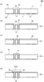
The electronic apparatus includes a printed circuit board and an electronic component mounted on the printed circuit board. In recent years, the mainstream of electronic parts are surface mount devices (SMDs (surface mount devices)) such as chip inductors, chip resistors, chip capacitors, and transistors.
Fig. 1(a) to 1(e) and fig. 2(a) to 2(e) are sectional views illustrating an assembling process of the electronic apparatus. Fig. 1(a) depicts a printed circuit board 10 with no components yet installed. On the first surface (front mounting surface) S1 and the second surface (rear mounting surface) S2 of the printed circuit board 10, printed wirings (not shown) and pads (pads) 12 and 14 are formed. The pads 12 and 14 are disposed at positions corresponding to the electrodes of the component, and portions other than the pads 12 and 14 are covered with the resist 11.
As shown in fig. 1(b), a screen (also referred to as a metal mask or a solder mask) 20 is placed on the first surface S1. The screen 20 has the openings 22, and the openings 22 are positioned to overlap the pads 12 provided on the first surface S1 side. Subsequently, as shown in fig. 1(c), a solder paste (flux) 30 is applied from above the screen 20. When the screen 20 is removed as shown in fig. 1(d), the solder paste 32 remains only on the pads 12.
Next, as shown in fig. 1(e), the component 40 is mounted on the first surface S1 by using a mounting machine. The solder paste 32 is sandwiched between the electrodes E1 and E2 of the component 40 and the pads 12. In this state, a reflow process is performed so that the component 40 is electrically and mechanically connected to the circuit board 10.
Next, mounting of the component on the second surface S2 is described. As shown in fig. 2(a), the printed circuit board 10 is turned upside down such that the second surface S2 faces upward. As shown in fig. 2(b), the screen 50 is then placed on the second surface S2. The screen 50 has the openings 52, and the openings 52 are positioned to overlap the pads 14 provided on the second surface S2 side. Subsequently, as shown in fig. 2(c), the solder paste 60 is applied from above the screen 50. When the screen 50 is removed as shown in fig. 2(d), the solder paste 62 remains only on the pads 14.
Then, as shown in fig. 2(e), the component 70 is mounted on the second surface S2 by using a mounting machine. The solder paste 62 is sandwiched between the electrodes E1 and E2 of the component 70 and the pads 14. In this state, a reflow process is performed so that the component 70 is electrically and mechanically connected to the circuit board 10. Surface mounting is as described above.
Disclosure of Invention
[ problem ] to
As a result of conducting research on surface mounting, the inventors of the present invention have recognized the following problems of surface mounting. The printed circuit board 10 includes a plurality of wiring layers, and different wiring layers are connected to each other through vias. The vias are typically located apart from the pads. However, in some cases, in order to improve heat dissipation or reduce parasitic impedance, a via is provided in the pad. The via provided in the pad is referred to as an intra-pad via.
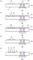
According to the conventional surface mounting technology, it is difficult to form the in-pad via on the first surface S1 as the preceding mounting surface. Fig. 3(a) to 3(e) are schematic views showing mounting of components on the first surface S1. Fig. 4(a) to 4(e) are schematic views showing mounting of components on the second surface S2.
Fig. 3(a) depicts a printed circuit board 10A with no components yet mounted. The lands (pads) 16 and the intra-land via holes 17 are formed on the first surface (the preceding mounting surface) S1 of the printed circuit board 10A.
The screen 20 is placed on the first surface S1 (fig. 3(b)), and then the solder paste 30 is applied from above the screen 20 (fig. 3 (c)). Subsequently, when the screen 20 is removed, the solder paste 32 remains on the pads 16 (fig. 3 (d)).
Next, the component 40A is mounted on the first surface S1 by using a mounting machine (fig. 3 (e)). The component 40A has a back surface electrode E3. The solder paste 32 is sandwiched between the back surface electrode E3 and the pad 16. In this state, a reflow process is performed so that the component 40A is electrically and mechanically connected to the circuit board 10. In this process, a part of the solder paste 32 passes through the in-pad through-hole 17 (via hole) and leaks from the second surface S2 side. Solder leakage 34 results in a failed installation, as described below.
Mounting of the component on the second surface S2 is described below with reference to fig. 4(a) to 4 (e). As shown in fig. 4(a), the printed circuit board 10A is turned upside down such that the second surface S2 faces upward. Next, as shown in fig. 4(b), the screen 50 is placed on the second surface S2. The screen 50 has openings 52, the openings 52 being positioned to overlap the pads 14.
Subsequently, as shown in fig. 4(c), the solder paste 60 is applied from above the screen 50. Fig. 4(d) depicts a state where the screen 50 is removed. The solder paste 62 is applied to unintended areas other than the pads 14. When the component 70 is mounted on the second surface S2 in this state and then subjected to a reflow process, the pads 14 adjacent to each other may cause a short circuit or other failure due to the solder paste 62.
The above problems may occur due to the use of conventional surface mounting techniques. In the case where the in-pad through-holes are to be formed on the preceding mounting surface, it is conceivable that mounting of the component on the second surface may be performed by selectively applying solder paste to the pads 14 using a needle dispenser without using a screen printing process. This method makes it possible to mount components on the second surface S2 while avoiding the influence of the solder paste 30 on the first surface S1. However, applying solder paste with a needle dispenser results in significantly lower throughput compared to solder paste application with a screen printing process. Therefore, in the case where a large number of components are to be mounted on the second surface S2, the solder paste should not be applied with the needle dispenser.
As another method, it is conceivable that, in the process of manufacturing the printed circuit board 10A, the through holes are filled with metal or resin in advance to close the holes. In this way, the solder paste 30 can be prevented from leaking to the second surface S2 side in the process shown in fig. 3 (e). However, using this solution increases the number of steps required to manufacture the printed circuit board 10A. As a result, the cost of the printed circuit board 10A increases.
The present invention has been made in view of the above circumstances. An exemplary object of an aspect of the present invention is to provide a surface mounting technique capable of solving the problem caused by the via-in-pad.
[ solution of problem ]
One aspect of the present invention relates to a method of manufacturing a semiconductor device. The manufacturing method includes a first step and a second step. The first step is to mount a first set of components on a first surface of the printed circuit board. The second step is to mount a second set of components on a second surface of the printed circuit board. The printed circuit board has an intra-pad via. The first step includes a step of applying solder paste to a plurality of pads on the first surface, a step of mounting the first component group on the first surface, and a step of heating and cooling the printed circuit board. The second step includes a step of placing a screen (metal mask) having openings at the positions of the plurality of pads on the second surface and having recesses positioned to overlap the through-holes in the pads on the second surface, a step of applying solder paste from above the screen and removing the screen, a step of mounting the second component group on the second surface, and a step of heating and cooling the printed circuit board.
Another aspect of the invention relates to a screen. The screen is used when a component is to be mounted on a printed circuit board having through-holes in pads. The screen includes a plurality of openings and recesses. The openings are provided at positions corresponding to a plurality of pads formed on the printed circuit board. The recess is positioned to overlap the in-pad via.
Still another aspect of the present invention relates to a method of manufacturing a semiconductor device having a voltage stabilization module. The manufacturing method includes a first step and a second step. The first step is to mount a first component group including a power transistor on a first surface of the printed circuit board. The second step is to mount a second component group including the inductor on a second surface of the printed circuit board. The printed circuit board has an intra-pad via. The intra-pad via is positioned to overlap the back surface electrode of the power transistor. The first step includes a step of applying solder paste to a plurality of pads on the first surface, a step of mounting the first component group on the first surface, and a step of heating and cooling the printed circuit board. The second step includes a step of placing a screen having openings at positions of a plurality of pads on the second surface and having recesses positioned to overlap the through-holes in the pads on the second surface, a step of applying solder paste from above the screen and removing the screen, a step of mounting the second component group on the second surface, and a step of heating and cooling the printed circuit board.
It should be noted that any combination of the above-described component elements and expressions of the present invention, as converted between, for example, methods, apparatus and systems, is also effective as an aspect of the present invention.
[ advantageous effects of the invention ]
The present invention makes it possible to solve the problems caused by the via-in-pad.
Drawings
Fig. 1(a) to 1(e) are sectional views illustrating an assembling process of the electronic apparatus.
Fig. 2(a) to 2(e) are sectional views illustrating an assembling process of the electronic apparatus.
Fig. 3(a) to 3(e) are schematic views showing mounting of components on the first surface S1.
Fig. 4(a) to 4(e) are schematic views showing mounting of components on the second surface S2.
Fig. 5(a) to 5(e) are diagrams illustrating an electronic device manufacturing method according to an embodiment.
Fig. 6(a) to 6(e) are diagrams illustrating an electronic device manufacturing method according to an embodiment.
Fig. 7 is a circuit diagram showing a configuration example of a multiphase step-down DC (direct current)/DC converter.
Fig. 8(a) to 8(c) are waveform diagrams each showing switching voltages Vsw1 to Vsw4 generated when K is 2, 3, or 4.
Fig. 9(a) is a layout view showing a back surface electrode of the power module, and fig. 9(b) is a layout view showing a back surface electrode of the inductor.
Fig. 10 is a layout diagram showing a DC/DC converter according to a comparative technique.
Fig. 11 is a diagram illustrating a wiring pattern of a printed circuit board according to a comparative technique.
Fig. 12(a) and 12(b) are layout diagrams showing a DC/DC converter according to example 1-1.
Fig. 13 is a diagram showing a wiring pattern of a DC/DC converter according to example 1-1.
Fig. 14 is a perspective view showing the DC/DC converter viewed from the sub-mounting surface SB side.
Fig. 15(a) and 15(b) are sectional views showing a heat sink according to a first configuration example.
Fig. 16(a) and 16(b) are sectional views showing a heat sink according to a second configuration example.
Fig. 17(a) and 17(b) are layout diagrams showing the DC/DC converter according to examples 1-2.
Fig. 18 is a diagram showing a wiring pattern of a DC/DC converter according to example 1-2.
Fig. 19(a) and 19(b) are layout diagrams showing DC/DC converters according to examples 1 to 3.
Fig. 20(a) and 20(b) are layout diagrams showing DC/DC converters according to examples 1 to 4.
Fig. 21 is an equivalent circuit diagram showing a DC/DC converter according to the second embodiment.
Fig. 22(a) and 22(b) are layout diagrams showing a DC/DC converter according to example 2-1.
Fig. 23 is a diagram showing a wiring pattern of a DC/DC converter according to example 2-1.
Fig. 24(a) and 24(b) are layout diagrams showing the DC/DC converter according to example 2-2.
Fig. 25(a) and 25(b) are layout diagrams showing DC/DC converters according to examples 2 to 3.
Detailed Description
The present invention will now be described in accordance with preferred embodiments with reference to the accompanying drawings. The same or equivalent constituent elements, components and processes described in the drawings are denoted by the same reference numerals and are not described again where appropriate. Furthermore, the embodiments are illustrative and not restrictive. All features described in connection with the embodiments and combinations thereof are not necessarily essential to the invention.
Further, dimensions (e.g., thickness, length, and width) may be exaggerated or minimized as appropriate in some cases to facilitate understanding. Further, the sizes of the plurality of members do not always indicate the size relationship therebetween. For example, even though member a is thicker than member B in the figures, member a may be thinner than member B.
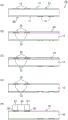
Fig. 5(a) to 5(e) and fig. 6(a) to 6(e) are diagrams illustrating an electronic device manufacturing method according to an embodiment. Fig. 5(a) to 5(e) and fig. 6(a) to 6(e) describe an assembly process by surface mounting.
The mounting of the component on the first surface S1 will now be described with reference to fig. 5(a) to 5 (e). As described below, the mounting on the first surface S1 is substantially similar to the mounting shown in fig. 3(a) to 3 (e).
Fig. 5(a) depicts a printed circuit board 10B to which no component has been mounted. Some of the pads (lands) 12 and 16 are formed on the first surface (front mounting surface) S1 of the printed circuit board 10B. An intra-pad via 17 is formed in the pad 16. Some of the pads 14 and 18 are similarly formed on the second surface (rear mounting surface) S2 of the printed circuit board 10B. An intra-pad via 19 is formed in the pad 18.
As shown in fig. 5(b), the screen 20 is placed on the first surface S1. The screen 20 has openings 22 and 24, and the openings 22 and 24 are provided at positions corresponding to the pads 12 and 16. Subsequently, the solder paste 30 is applied from above the screen 20 (fig. 5 (c)).
Next, when the screen 20 is removed, the solder paste 32 remains on the pads 12 and 16 (fig. 5 (d)).
Subsequently, the components 40 and 40A are mounted on the first surface S1 by using a mounting machine (fig. 5 (e)). The solder paste 32 is sandwiched between the electrodes E1 and E2 of the component 40 and the pads 12. The component 40A has the back surface electrode E3, and the solder paste 32 is sandwiched between the back surface electrode E3 and the pad 16. In this state, a reflow process is performed so that the component 40A is electrically and mechanically connected to the circuit board 10.
In the above process, a part of the solder paste 32 passes through the in-pad through-hole 17 (via hole) and leaks from the second surface S2 side.
Next, mounting of the components on the second surface S2 will be described with reference to fig. 6(a) to 6 (e). As shown in fig. 6(a), the printed circuit board 10B is turned upside down such that the second surface S2 faces upward. Next, as shown in fig. 6(B), the screen 50B is placed on the second surface S2.
In the present embodiment, the screen 50B has the openings 52 positioned to overlap the pads 14. Further, a concave portion 56 provided so as to overlap with the in-pad through hole 19 is formed on the screen 50B. The recesses 56 prevent the screen 50B from interfering with the solder leakage 34, and make it possible for the screen 50B to be in close contact with the second surface S2.
Fig. 6(d) depicts a state in which the screen 50B is removed. The solder paste 62 is applied only to the pads 14 and 18, and is suppressed from excessively protruding from the pads 14 and 18.
Subsequently, as shown in fig. 6(e), the components 70 and 70A are mounted on the second surface S2, and then a reflow process is performed. This makes the electrodes E1 and E2 of the component 70 electrically and mechanically connected to the pads 14, and makes the back surface electrode E3 of the component 70A electrically and mechanically connected to the pads 18. The semiconductor device 100 is assembled in the above manner.
The semiconductor device manufacturing method according to the embodiment is as described above.
As described above, according to the present embodiment, in order to avoid interference with the solder leakage 34, the recesses 56 are formed on the screen 50B, which screen 50B is used when solder paste is applied to the second surface S2. This makes it possible to avoid the positional displacement of the screen 50B due to the solder leakage 34 and prevent the solder paste 60 from entering the gap between the screen 50B and the second surface S2.
It should be noted that when the component 70A is mounted on the second surface S2, the solder leak 64 may occur on the first surface S1 side through the in-pad via 19. However, such solder leakage 64 does not adversely affect because the mounting of the component on the first surface S1 is already completed.
Next, use of the manufacturing method according to the embodiment will be described. The manufacturing method according to this embodiment can be applied to the manufacturing process of the DC/DC converter described below. The above-described component 40A to be mounted on the first surface S1 corresponds to the later-described power module 220 to be mounted on the first surface S1.
In electronic devices such as personal computers and game consoles, a DC/DC converter (switching regulator) is used to reduce the direct voltage provided by a battery or an inverter to an optimum voltage level of a load.
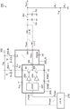
Fig. 7 is a circuit diagram showing a configuration example of the multiphase step-down DC/DC converter. The DC/DC converter 200 has N phases (N ≧ 2), and includes an input line 202, an output line 204, N inductors L1_1 to L1_ N, an input capacitor Ci, an output capacitor Co, a controller 210, and N power modules 220_1 to 220_ N.
The output line 204 is connected to the power consumption (load current I)OUT) A dynamically changing load (not shown). The DC/DC converter 200 receives an input voltage V of an input line 202INGenerating an output voltage V stabilized at a predetermined levelOUTAnd the output voltage V to be generatedOUTTo a load. The input line 202 is connected to a voltage regulator for stabilizing the input voltage VINThe input capacitor Ci. The output line 204 is connected to a smoothing output voltage VOUTThe output capacitor Co.
The power module 220 mainly has a VIN pin, a PGND pin, a SW pin, a VCC pin, an AGND pin, and a PWM pin. The power module 220 includes a high-side switch (switching transistor) M1, a low-side switch (synchronous rectifier transistor) M2, a high-side driver 222, a low-side driver 224, and a logic circuit 226. A high-side switch M1 is provided between the VIN and SW pins. A low side switch M2 is provided between the SW pin and the PGND pin.
The controller 210 monitors the current or load current I flowing to each of the plurality of inductors L1_1 through L1_ NOUTAnd determines the number of drive phases K. For example, in the case where N is 4, four values, i.e., 1, 2, 3, and 4 (or three values, i.e., 1, 2, and 4) may be selected as the driving phase number K.
Further, the controller 210 receives the voltage V based on the output voltageOUTIs fed back toFBThe generated duty ratio is adjusted so that the feedback signal VFBApproaching a predetermined target voltage VREFPulse signal S ofPWMAnd generating a pulse signal SPWMTo K power modules of the N power modules 220_1 to 220_ N. Pulse signal S with phase difference of 360/K degreesPWM1To SPWMKAre allocated to K power modules 220_1 to 220_ K.
The DC/DC converter 200 is configured as described above. Next, the operation of the DC/DC converter 200 is described below. The following description relates to the case where M ═ 4 and the drive phase number K may be 2, 3, or 4. Fig. 8(a) to 8(c) are waveform diagrams each showing switching voltages Vsw1 to Vsw4 generated when K is 2, 3, or 4.
The components of the DC/DC converter 200 are mounted on a printed circuit board. The conventional DC/DC converter 200 is configured such that the inductors L1_1 to L1_ N and the power modules 220_1 to 220_ N, which are main components, are mounted on the same mounting surface. Here, the main component means a component that occupies a large area and allows a large current to flow.
Mounting the main components on the same mounting surface enlarges the area occupied by the DC/DC converter 200. It means an increase in the area of the printed circuit board and may lead to an increase in cost.
Further, in the case of an application that causes the plurality of power modules 220_1 to 220_ N to generate a large amount of heat, it is necessary to cool the plurality of power modules 220_1 to 220_ N using a heat sink. However, when the plurality of power modules 220_1 to 220_ N are disposed near other components such as the plurality of inductors L1_1 to L1_ N, the shape of the heat sink may be restricted by the other components to impair the cooling effect.
In contrast, determining the layout by prioritizing the cooling effect increases the distance between the power module and the inductor, and enlarges the area occupied by the DC/DC converter 200. This may result in increased costs.
(first embodiment)
One aspect of the invention is understood to be a DC/DC converter layout or mounting technique. In the first embodiment, the function or equivalent circuit of the DC/DC converter is similar to that of the converter shown in fig. 7.
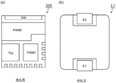
Some examples of common power modules 220 will now be described. The power module 220 is well known per se and is manufactured and sold by various IC manufacturers.
The circuit configuration of the power module 220 is similar to that shown in fig. 1. More specifically, the power module 220 includes a high-side transistor M1, a low-side transistor M2, a high-side driver 222, a low-side driver 224, and a logic circuit 226. In addition, the power module 220 has, for example, an input (VIN) pin, a switch pin (SW), a ground pin (PGND, AGND), a power supply (VCC) pin, and a control (PWM) pin. It should be noted that the power module 220 additionally includes, for example, a bootstrap circuit and various protection circuits and a number of pins associated with these circuits. However, since they are not related to the present invention, they are neither depicted in the drawings nor described below.
Supply voltage VCCProvided to the logic circuit 226 and various other circuit blocks through the VCC pin. For example, the AGND pin is ground for the high side driver 222, the low side driver 224, and the logic circuit 226. DC input voltage VINIs provided to the VIN pin. The PGND pin is the ground of the output stage.
The logic circuit 226 is based on the PWM signal S input to the PWM pinPWMGenerating a high side pulse and a low side pulse. The high-side driver 222 drives the high-side transistor M1 based on the high-side pulse. The low side driver 224 drives the low side transistor M2 based on the low side pulse.
The pin arrangement of each main circuit component package will now be described. Fig. 9(a) is a layout diagram showing the back surface electrode of the power module 220. As previously described, the power module 220 has a VIN pin, a PGND pin, a SW pin, a VCC pin, and an AGND pin. Of these pins, the area of the VIN pin and the GND pin is relatively larger than that of the other pads. Especially the PGND and AGND pins are large in area because they also serve as heat dissipation pads. The PWM pin and other control pins are assigned to the remaining pins. It should be noted that the layout of the back surface electrodes depicted in fig. 9(a) and 9(b) is merely illustrative and is significantly different for different chip suppliers and different products.
Fig. 9(b) is a layout diagram showing the back surface electrode of the inductor L1. The inductor L1 includes a first electrode E1 and a second electrode E2. The first electrode E1 and the second electrode E2 are disposed at the center of two opposite sides.
One of the tasks of the embodiment is to provide an improved layout. Therefore, first, a layout (hereinafter referred to as a comparison technique) serving as a basis of comparison will be described.
In recent years, electronic circuits are mounted by using a surface mount technology (SMT (surface mount technology)). Surface mounting is achieved by applying solder paste to pads (pads) formed on a printed circuit board, mounting components using a mounter, and then performing a reflow process.
In the case of surface mounting components on both surfaces of a printed circuit board, some components are first mounted on one surface (the preceding mounting surface). Then, with the printed circuit board inverted, other components are mounted on the other surface (the rear mounting surface). When the reflow process is performed on the rear mounting surface, the solder on the front mounting surface is reheated. If the components mounted on the front mounting surface are heavy or large, the mounted components may be dislodged or fall off. Therefore, the components mountable on the front mounting surface are limited in size and weight. Therefore, the front mounting surface is generally used as a sub-mounting surface. That is, a relatively small number, lighter, or smaller sized components are mounted on the sub-mounting surface, while a relatively large number, heavier, or larger sized components are mounted on the main mounting surface. The DC/DC converter is no exception, and therefore all components are basically mounted on the main mounting surface even if the comparative technique is used.
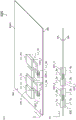
Fig. 10 is a layout diagram showing a DC/DC converter according to a comparative technique. In the example shown in fig. 10, N is assumed to be 3. The controller 210, the power modules 220_1 to 220_ N, the input capacitor Ci, and the output capacitor Co (these are referred to as main components) are arranged on the main mounting surface SA of the printed circuit board 300R.
The plurality of inductors L1_1 to L1_ N are linearly arranged in a first direction (x direction) of the printed circuit board. The power modules 220 # (# ═ 1, 2. -, N) are disposed adjacent to the corresponding inductors L1 #) in the second direction (y-direction). This can reduce the parasitic resistance between the power module 220_ # and the inductor L1_ #.
Fig. 11 is a diagram showing a wiring pattern of a printed circuit board 300R according to the comparative technique. In fig. 11, the through holes are marked with circles. A plurality of pattern wirings (printed wirings) PTN1_1 to PTN1_3, PTN _2, PTN3_1 to PTN3_3, PTN4 are formed on the printed circuit board 300. The first pattern wirings PTN1_1 to PTN1_3 correspond to the input lines 202_1 to 202_3 shown in fig. 7. An input pin VIN of the power module 220 # (# ═ 1, 2. -, N) is connected to a corresponding pad of the first pattern wiring PTN1 #.
The second pattern wiring PTN2 is a ground plane, and is formed to be shared by all the phases in order to keep the impedance as low as possible. The ground pin PGND of the power module 220 # (# ═ 1, 2.., N) is connected to the corresponding pad of the second pattern wiring PTN 2.
The input capacitor Ci _ # is disposed between the first pattern wiring PTN1_ # and the second pattern wiring PTN 2. The input capacitor Ci _ # may be an MLCC (multilayer ceramic capacitor) or an electrolytic capacitor, or a combination of these capacitors.
The third pattern wirings PTN3_1 to PTN3_3 are wirings for connecting the SW pin of the power module 220 to one end of the inductor L1 shown in fig. 7. The SW pin SW of the power module 220 # (# ═ 1, 2, …, N) is connected to the corresponding pad of the third pattern wiring PTN3 #. Further, the electrode E1 of the inductor L1 # (# ═ 1, 2, ·, N) is connected to the corresponding pad of the third pattern wiring PTN3 #.
The fourth pattern wiring PTN4 corresponds to the output line 204 shown in fig. 7. The electrode E2 of the inductor L1 # (# ═ 1, 2, …, N) is connected to the corresponding pad of the fourth pattern wiring PTN 4. An output capacitor Co (not shown in fig. 11) shown in fig. 7 is connected between the fourth pattern wiring PTN4 and the ground plane.
The resistances of the first to fourth pattern wirings PTN1 to PTN4 need to be as low as possible because a large current flows in the first to fourth pattern wirings PTN1 to PTN 4. Therefore, these pattern wirings PTN1 to PTN4 each form a multilayer wiring and are connected to wirings in different wiring layers not shown in fig. 11 through vias.
The component layout according to the comparative technique is as described above. The component layout according to the embodiment will now be described. In the present embodiment, it is assumed that at least one of the N power modules 220 is mounted on the sub-mounting surface SB of the printed circuit board 300. The sub-mounting surface SB is opposite to the main mounting surface SA of the printed circuit board 300. Some examples of the present embodiment are described below.
(example 1-1)
Fig. 12(a) and 12(b) are layout diagrams showing the DC/DC converter 200A according to example 1-1. Fig. 12(a) is a perspective view, and fig. 12(b) is a sectional view. In example 1-1, all the power modules 220_1 to 220_3 are mounted on the sub-mounting surface SB. Preferably, the input capacitor Ci _ # is connected immediately to the VIN pin of the power module 220_ #. Therefore, in example 1-1, the input capacitor Ci _ # is also mounted on the sub-mounting surface SB.
Fig. 13 is a diagram showing a wiring pattern of the DC/DC converter 200A according to example 1-1. In fig. 13, components to be mounted on the main mounting surface SA are indicated by broken lines, and components to be mounted on the sub-mounting surface SB are indicated by two-dot chain lines. The functions of the pattern wirings PTN1 to PTN4 are similar to those shown in fig. 11. Further, the pattern wirings PTN1 to PTN4 are multilayer wirings formed on the main mounting surface SA and the sub mounting surface SB (and in the intermediate wiring layer) to overlap each other, and are electrically connected to each other through vias.
The DC/DC converter 200A according to example 1-1 is configured as described above. The use of the sub-mounting surface SB to mount the power module 220 provides additional space on the main mounting surface SA or the sub-mounting surface SB. This results in the following advantages.
Fig. 14 is a perspective view showing the DC/DC converter 200A viewed from the sub-mounting surface SB side.
The DC/DC converter 200A includes a heat sink 240. Radiator 240 and a plurality of power modules 220_1 to 220
220_3 are in contact with each other. There is no component higher than the power module 220 near the power modules 220_1 to 220_ N on the sub-mounting surface SB side. Accordingly, a large-sized heat sink 240 may be included in the DC/DC converter 200A to provide increased cooling efficiency.
A configuration example of the heat sink will now be described in detail. Fig. 15(a) and 15(b) are sectional views showing a heat sink 240A according to a first configuration example. Fig. 15(a) depicts a state in which the heat sink 240A is applied to example 1-1. Fig. 15(b) depicts a state in which the same heat sink 240A is applied to the comparative technique depicted in fig. 10.
The heat sink 240A includes a heat dissipation portion 242 and a contact portion 244. The heat dissipation portion 242 has an opening in which the contact portion 244 is fitted. The contact portion 244 is in contact with the power module 220 to be cooled.
Example 1-1 is now compared to a comparative technique. As shown in fig. 15(b), the comparative technique for mounting the power module 220 on the main mounting surface SA is configured such that a high component 221 (e.g., an inductor) exists in the vicinity of the power module 220. Therefore, it is difficult to position the heat dissipation portion 242 near the surface of the printed circuit board. This increases the height of the contact portion 244 in the Z direction. This results in an increase in thermal resistance, resulting in a decrease in cooling performance.
On the other hand, in example 1-1 in which the power module 220 is mounted on the sub-mounting surface SB, as shown in fig. 15(a), there is no tall component near the power module 220. Accordingly, the heat dissipation portion 242 may be located near the surface of the printed circuit board. This makes it possible to reduce the height of the contact portion 244 in the Z direction. As a result, the thermal resistance can be reduced to provide improved cooling performance.
Fig. 16(a) and 16(B) are sectional views showing a heat sink 240B according to a second configuration example. The heat sink 240B includes a heat radiating plate 246 and has projections 248 subjected to a stretching process. At the protrusion 248, the heat dissipation plate 246 is in contact with the surface of the power module 220.
Example 1-1 was compared to a comparative technique. As shown in fig. 16(b), the comparison technique is configured such that a high component 221 (e.g., an inductor) exists near the power module 220. Since the projection 248 interferes with the member 221, it is difficult for the comparative technique to adopt the second configuration example.
On the other hand, in example 1-1 in which the power module 220 is mounted on the sub-mounting surface SB, there is no part that interferes with the protrusion 248 of the heat sink 240B in the vicinity of the power module 220. This increases the degree of freedom in design of the heat sink 240B, and makes it possible to employ the heat sink 240B according to the second configuration example.
The cost of the heat sink 240B in fig. 16(a) and 16(B) can be reduced because it is simpler in structure than the heat sink 240A in fig. 15(a) and 15 (B). Further, the heat sink 240B in fig. 16(a) and 16(B) does not need any opening. Therefore, the heat sink 240B in fig. 16(a) and 16(B) has excellent electromagnetic noise shielding performance, and can improve EMC (electromagnetic compatibility).
(examples 1-2)
The DC/DC converter 200B according to example 1-2 will now be described with reference to the case where N ═ 4. Fig. 17(a) and 17(B) are layout diagrams showing the DC/DC converter 200B according to examples 1-2. Fig. 17(a) is a perspective view, and fig. 17(b) is a sectional view. In example 1-2, N power modules 220_1 to 220_ N are alternately mounted on the main mounting surface SA and the sub-mounting surface SB. More specifically, odd-numbered power modules 220 # (# ═ 1, 3.) are mounted on the sub-mounting surface SB, and even-numbered power modules 220 __ 2, 4..) are mounted on the main mounting surface SA. The reverse is also possible.
Fig. 18 is a diagram showing a wiring pattern of the DC/DC converter 200B according to example 1-2. In fig. 18, components to be mounted on the main mounting surface SA are indicated by broken lines, and components to be mounted on the sub-mounting surface SB are indicated by two-dot chain lines. The functions of the pattern wirings PTN1 to PTN4 are as described previously. Further, the pattern wirings PTN1 to PTN4 are multilayer wirings formed on the main mounting surface SA and the sub mounting surface SB (and in the intermediate wiring layer) to overlap each other, and are electrically connected to each other through vias.
In examples 1-2, N power modules are configured such that a first and second module are paired, a third and fourth module are paired, and so on. Further, the pair of two power modules 220_ i and 220_ j are connected to a common input line (i.e., a common first pattern wiring line PTN1_ i, j).
When all the power modules 220 are mounted on the same mounting surface, as in the case of example 1-1 or the comparative technique, it is necessary to form the first pattern wiring PTN1 for each power module 220. On the other hand, as described in examples 1-2, when the power module 220 is alternately mounted on the main mounting surface SA and the sub-mounting surface SB, the VIN terminals are positioned adjacent to each other. This is advantageous because a common input line can be used.
Further, using the common input line (the first pattern wiring PTN1_ i, j) provides an advantage that the common input capacitor Ci _ i, j can also be used. More specifically, the input capacitors Ci _ i, j on the main mounting surface SA function as both the input capacitor of the power module 220_ i and the input capacitor of the power module 220_ j on the sub-mounting surface SB side. This makes it possible to double the effect of the input capacitor. Alternatively, the number of capacitors required to obtain the same effect as the input capacitor may be reduced to reduce the cost.
(examples 1 to 3)
Fig. 19(a) and 19(b) are layout diagrams showing the DC/DC converter 200D according to examples 1 to 3. In examples 1 to 3, the chip size of the inductor used in examples 1 to 2 was reduced. In the case of an application in which a small current flows to the inductor L1, a component having a small allowable current, that is, a component having a small chip size can be selected, and thus the area occupied by the component is reduced.
(examples 1 to 4)
Fig. 20(a) and 20(b) are layout diagrams showing the DC/DC converter 200G according to examples 1 to 4. In examples 1-4, the layout of the inductors used in examples 1-3 was changed. More specifically, the inductor L1_1 in examples 1 to 4 is mounted on the same surface as the corresponding power module 220_ i. Accordingly, the inductor L1_ i may be connected to the corresponding power module 220_ i with a low impedance.
More preferably, a pair of inductors L1_1 and L1_2 are mounted on both surfaces SA and SB of the printed circuit board 300G in an overlapping manner. Further, a pair of inductors L1_3 and L1_4 are mounted on both surfaces SA and SB of the printed circuit board 300G in an overlapping manner. This makes it possible to enlarge the interval between adjacent inductors and to alleviate the heat concentration, as compared with the layout shown in fig. 19(a) and 19 (b).
(second embodiment)
As described in connection with examples 1-3, in the case of an application in which a small coil current flows to the inductor L1, the chip size can be reduced. However, in the case of an application in which a large coil current flows to the inductor L1, there is no choice but to select an element having a large allowable current, i.e., a component having a large chip size. Therefore, the size occupied by the DC/DC converter is limited by the inductor chip size. The second embodiment is described below by explaining a technique of reducing the size occupied by the DC/DC converter in the application case where a large coil current flows.
Fig. 21 is an equivalent circuit diagram showing a DC/DC converter 200C according to the second embodiment. In the DC/DC converter 200C, the inductor L1_ # (# ═ 1, 2,. and N) is formed by connecting two inductor chips L1_ # a and L1_ # b having the same inductance value and chip size in parallel, respectively.
The inductance value of the two parallel connected inductor chips is 1/2 times the inductance value of the single inductor chip. Meanwhile, the amount of current flowing to the two parallel-connected inductor chips is 1/2 times the amount of current flowing to the single inductor chip. In the second embodiment, an inductor chip having a small current capacity, i.e., an inductor chip having a small package size, can be selected by reducing the amount of current per chip. For example, in the case where a single 10 mm square inductor chip is to be employed, the technical idea of the second embodiment may be introduced to employ two 6 mm square inductor chips in parallel instead of the single 10 mm square inductor chip.
When a product mounted with the DC/DC converter 200 is to be mass-produced, it is necessary to consider the usability of the chip parts. In particular, in the case where products are to be mass-produced and sold for a long time, the chip parts need to be stably supplied for a long time. Currently, the size of chip components is gradually reduced, and more kinds of small-sized inductor chips are produced. On the other hand, the usability of large-sized chip components is reduced. In this regard, the problem of usability can be solved by replacing the conventionally employed inductor having a large chip size with a plurality of parallel-connected inductor chips having a small chip size.
(example 2-1)
Fig. 22(a) and 22(b) are layout diagrams showing the DC/DC converter 200C according to example 2-1. Fig. 22(a) is a perspective view, and fig. 22(b) is a sectional view.
Two inductor chips L1_ # a and L1_ # b electrically connected in parallel with each other are mounted on the main mounting surface SA and the sub-mounting surface SB of the printed circuit board 300C in an overlapping manner.
In example 2-1, as in the case of example 1-2 of the first embodiment, N power modules 220_1 to 220 — N are alternately mounted on the main mounting surface SA and the sub-mounting surface SB.
Fig. 23 is a diagram showing a wiring pattern of the DC/DC converter 200C according to example 2-1. The length (total width) W of the area occupied by the DC/DC converter in the X direction is mainly limited by the width W of the sensor chip. More specifically, W ═ W × N + s × (N-1), where s denotes the interval between the sensor chips in the x direction. For example, if a 10 mm square inductor chip is replaced with a 6 mm square inductor chip in the case of N-4, the total width of the area occupied by the DC/DC converter can be reduced by about 4 mm × 4-16 mm.
Further, example 2-1 provides the same advantages as example 1-2. That is, a common input line may be used for two adjacent phases, and additionally a common input capacitor Ci _ i, j may be used for the two adjacent phases.
(example 2-2)
Fig. 24(a) and 24(b) are layout diagrams showing the DC/DC converter 200E according to example 2-2. Fig. 24(a) is a perspective view, and fig. 24(b) is a sectional view. Example 2-2 is similar to example 1-1 in fig. 12(a) and 12(b), in which a plurality of power modules 220_1 to 220_4 are mounted on the sub-mounting surface SB. Although not described in fig. 24(a) and 24(b), the input capacitor Ci should be mounted on the sub-mount surface SB as in the case of example 1-1.
As in the case of example 2-1, example 2-2 makes it possible to reduce the area occupied by the DC/DC converter 200E.
(examples 2 to 3)
Fig. 25(a) and 25(b) are layout diagrams showing the DC/DC converter 200F according to examples 2 to 3. Fig. 25(a) is a perspective view, and fig. 25(b) is a sectional view. In example 2-3, the plurality of power modules 220_1 to 220_4 are all mounted on the main mounting surface SA.
As in the case of examples 2-1 and 2-2, example 2-3 makes it possible to reduce the area occupied by the DC/DC converter 200F.
(modification 2-1)
In examples 2-1 to 2-3, the inductor L1 of each phase is formed by connecting two inductor chips in parallel. However, the number of inductor chips is not limited to two. The inductor L1 for each phase may alternatively be formed by connecting three or more inductor chips in parallel.
(mounting technique)
Next, a technique for mounting the power module 220 will be described. Referring to fig. 7, the DC/DC converter 200 is preferably configured such that the inductive and resistive components of the input line 202 are as small as possible. Furthermore, the PGND pin is preferably grounded with as low impedance as possible. As shown in fig. 11 and 13, pads (pads) for soldering the VIN pins are formed on the first pattern wiring PTN1, and pads (pads) for soldering the PGND pins are formed on the second pattern wiring PTN 2. With the multilayer wiring, a large number of vias are provided to reduce the resistance of the pattern wirings PTN1 and PTN 2. However, in order to keep the resistance as low as possible, it is necessary to form a via hole in a pad (bonding pad). These vias are referred to as intra-pad vias.
When the comparative technique is as shown in fig. 11, the power module 220 is mounted only on the main mounting surface. Therefore, forming the intra-pad via hole is not particularly difficult. However, in examples 1-1, 1-2, 1-3, 2-1, and 2-2, the intra-pad via needs to be formed on the sub-mount surface because the power module 220 is mounted on the sub-mount surface. It is not impossible to form the intra-pad via on the sub-mount surface if the cost is not considered. However, when considering the cost, the intra-pad via will not be easily formed on the sub-mounting surface by using the conventional surface mounting technology. The surface mount techniques described in connection with the embodiments are suitable for mounting power modules 220 that require through-holes in the pads.
The invention has been described in terms of embodiments. These examples are illustrative and not restrictive. It will be understood by those skilled in the art that various modifications may be made in the combination of the component elements and processes of the embodiments and that such modifications are also within the scope of the present invention.
[ Industrial Applicability ]
The present invention relates to surface mount technology.
[ list of reference numerals ]
10: printed circuit board
12. 14, 16: bonding pad
17: via in pad
18: bonding pad
19: via in pad
S1: first surface
S2: second surface
20: silk screen
22: opening of the container
30: solder paste
32: solder paste
34: solder leakage
40: component part
E1, E2: electrode for electrochemical cell
E3: back surface electrode
50: silk screen
52, 54: opening of the container
56: concave part
60: solder paste
70: component part
Claims (4)
1. A method of manufacturing a semiconductor device, the method comprising:
a first step of mounting a first component group on a first surface of a printed circuit board; and
a second step of mounting a second component group on a second surface of a printed circuit board having an in-pad via hole,
the first step comprises:
a step of applying solder paste to the plurality of pads on the first surface;
a step of mounting a first component group on a first surface; and
a step of heating and cooling the printed circuit board, and
the second step includes:
a step of placing a screen (metal mask) having openings at positions of a plurality of pads on the second surface and having recesses positioned to overlap with the in-pad through-holes, on the second surface;
a step of applying solder paste from above the screen and removing the screen;
a step of mounting a second component group on a second surface; and
a step of heating and cooling the printed circuit board.
2. The manufacturing method according to claim 1, wherein
The first group of components includes power transistors, and
the intra-pad via is positioned to overlap a back surface electrode of the power transistor.
3. A screen for use in mounting a component on a printed circuit board having in-pad through-holes, the screen comprising:
a plurality of openings provided at positions corresponding to positions of a plurality of pads formed on the printed circuit board; and
a recess positioned to overlap the in-pad via.
4. A method of manufacturing a semiconductor device having a voltage stabilization module, the method comprising:
a first step of mounting a first component group including at least one power transistor on a first surface of a printed circuit board; and
a second step of mounting a second component set including at least one inductor on a second surface of the printed circuit board, wherein
The printed circuit board having an in-pad via positioned to overlap a back surface electrode of the power transistor,
the first step comprises:
a step of applying solder paste to the plurality of pads on the first surface;
a step of mounting a first component group on a first surface; and
a step of heating and cooling the printed circuit board, and
the second step includes:
a step of placing a screen on the second surface, the screen having openings at positions of a plurality of pads on the second surface and having recesses positioned to overlap with the in-pad through-holes;
a step of applying solder paste from above the screen and removing the screen;
a step of mounting a second component group on a second surface; and
a step of heating and cooling the printed circuit board.
Applications Claiming Priority (3)
| Application Number | Priority Date | Filing Date | Title |
|---|---|---|---|
| JP2018197714A JP7107810B2 (en) | 2018-10-19 | 2018-10-19 | Semiconductor device manufacturing method and screen |
| JP2018-197714 | 2018-10-19 | ||
| PCT/JP2019/041097 WO2020080525A1 (en) | 2018-10-19 | 2019-10-18 | Semiconductor device manufacturing method and screen |
Publications (1)
| Publication Number | Publication Date |
|---|---|
| CN112889355A true CN112889355A (en) | 2021-06-01 |
Family
ID=70283953
Family Applications (1)
| Application Number | Title | Priority Date | Filing Date |
|---|---|---|---|
| CN201980067236.8A Pending CN112889355A (en) | 2018-10-19 | 2019-10-18 | Semiconductor device manufacturing method and screen |
Country Status (4)
| Country | Link |
|---|---|
| US (1) | US11647593B2 (en) |
| JP (1) | JP7107810B2 (en) |
| CN (1) | CN112889355A (en) |
| WO (1) | WO2020080525A1 (en) |
Families Citing this family (2)
| Publication number | Priority date | Publication date | Assignee | Title |
|---|---|---|---|---|
| JP7250474B2 (en) * | 2018-10-19 | 2023-04-03 | 株式会社ソニー・インタラクティブエンタテインメント | power supply |
| JP6835788B2 (en) | 2018-10-19 | 2021-02-24 | 株式会社ソニー・インタラクティブエンタテインメント | Power supply |
Citations (5)
| Publication number | Priority date | Publication date | Assignee | Title |
|---|---|---|---|---|
| US4739919A (en) * | 1987-06-15 | 1988-04-26 | Northern Telecom Limited | Masking of circuit boards for wave soldering |
| JPH05275843A (en) * | 1992-03-26 | 1993-10-22 | Kofu Nippon Denki Kk | Method for printing cream solder and metal mask for printing cream solder |
| JPH06334323A (en) * | 1993-05-25 | 1994-12-02 | Sony Corp | Solder precoating method |
| US5373984A (en) * | 1993-09-27 | 1994-12-20 | Sundstrand Corporation | Reflow process for mixed technology on a printed wiring board |
| CN1505456A (en) * | 2002-12-05 | 2004-06-16 | 华为技术有限公司 | A printed circuit board and processing method thereof |
Family Cites Families (21)
| Publication number | Priority date | Publication date | Assignee | Title |
|---|---|---|---|---|
| US4761881A (en) * | 1986-09-15 | 1988-08-09 | International Business Machines Corporation | Single step solder process |
| JP2502663B2 (en) * | 1988-03-17 | 1996-05-29 | 松下電器産業株式会社 | Manufacturing method of printed wiring board |
| JPH0794619A (en) | 1993-09-20 | 1995-04-07 | Hitachi Ltd | Hybrid integrated circuit device |
| JP2001068833A (en) * | 1999-08-27 | 2001-03-16 | Minami Kk | Method for coating component-mounted substrate with adhesive |
| JP5142119B2 (en) * | 2006-09-20 | 2013-02-13 | 住友電装株式会社 | Method of manufacturing printed circuit board having heat dissipation structure and heat dissipation structure of printed circuit board manufactured by the method |
| US8264073B2 (en) | 2007-03-07 | 2012-09-11 | International Rectifier Corporation | Multi-phase voltage regulation module |
| TW200906254A (en) * | 2007-07-18 | 2009-02-01 | Universal Scient Ind Co Ltd | Method for a unitary plate coated with different solder-pastes and its mold-plate set |
| JP5328147B2 (en) | 2007-12-26 | 2013-10-30 | 株式会社ケーヒン | Power drive unit |
| JP2010124570A (en) | 2008-11-18 | 2010-06-03 | Toshiba Carrier Corp | Power conversion device |
| JP5420433B2 (en) | 2010-01-14 | 2014-02-19 | ルネサスエレクトロニクス株式会社 | Semiconductor device and power supply device |
| JP5974603B2 (en) | 2012-04-17 | 2016-08-23 | 株式会社村田製作所 | Inductor array chip and DC-DC converter |
| JP6162510B2 (en) | 2013-07-03 | 2017-07-12 | 株式会社ソニー・インタラクティブエンタテインメント | STEP-DOWN DC / DC CONVERTER, CONTROLLER AND CONTROL METHOD THEREOF, AND ELECTRONIC DEVICE USING THE SAME |
| JP6261071B2 (en) | 2013-10-15 | 2018-01-17 | オムロンオートモーティブエレクトロニクス株式会社 | Coil integrated printed circuit board, magnetic device |
| JP6334323B2 (en) | 2014-08-27 | 2018-05-30 | 東芝ライフスタイル株式会社 | Vacuum cleaner and its suction port |
| JP2016067164A (en) | 2014-09-25 | 2016-04-28 | 株式会社ノーリツ | Power conditioner |
| DE102015200716A1 (en) | 2015-01-19 | 2016-07-21 | Efficient Energy Gmbh | Switching Power Supply |
| JP6640544B2 (en) | 2015-12-14 | 2020-02-05 | 株式会社小糸製作所 | Light emitting module, lamp and circuit board for light emitting element |
| US10671009B2 (en) | 2017-02-13 | 2020-06-02 | Canon Kabushiki Kaisha | Printed circuit board mounting piezoelectric transformer |
| US10361631B2 (en) | 2017-10-05 | 2019-07-23 | Monolithic Power Systems, Inc. | Symmetrical power stages for high power integrated circuits |
| CN207573821U (en) | 2017-12-14 | 2018-07-03 | 苏州众能医疗科技有限公司 | A kind of two-sided water cooling plate heat dissipating device |
| US10505456B1 (en) | 2018-09-07 | 2019-12-10 | International Business Machines Corporation | Fully integrated multi-phase buck converter with coupled air core inductors |
-
2018
- 2018-10-19 JP JP2018197714A patent/JP7107810B2/en active Active
-
2019
- 2019-10-18 WO PCT/JP2019/041097 patent/WO2020080525A1/en active Application Filing
- 2019-10-18 US US17/284,820 patent/US11647593B2/en active Active
- 2019-10-18 CN CN201980067236.8A patent/CN112889355A/en active Pending
Patent Citations (5)
| Publication number | Priority date | Publication date | Assignee | Title |
|---|---|---|---|---|
| US4739919A (en) * | 1987-06-15 | 1988-04-26 | Northern Telecom Limited | Masking of circuit boards for wave soldering |
| JPH05275843A (en) * | 1992-03-26 | 1993-10-22 | Kofu Nippon Denki Kk | Method for printing cream solder and metal mask for printing cream solder |
| JPH06334323A (en) * | 1993-05-25 | 1994-12-02 | Sony Corp | Solder precoating method |
| US5373984A (en) * | 1993-09-27 | 1994-12-20 | Sundstrand Corporation | Reflow process for mixed technology on a printed wiring board |
| CN1505456A (en) * | 2002-12-05 | 2004-06-16 | 华为技术有限公司 | A printed circuit board and processing method thereof |
Also Published As
| Publication number | Publication date |
|---|---|
| US11647593B2 (en) | 2023-05-09 |
| US20210345496A1 (en) | 2021-11-04 |
| JP7107810B2 (en) | 2022-07-27 |
| WO2020080525A1 (en) | 2020-04-23 |
| JP2020065029A (en) | 2020-04-23 |
Similar Documents
| Publication | Publication Date | Title |
|---|---|---|
| US11824429B2 (en) | Multi-phase step-down DC/DC power source device | |
| US7304862B2 (en) | Printed wiring board having edge plating interconnects | |
| TWI400725B (en) | Apparatus and system having an integrated inductor | |
| US6940724B2 (en) | DC-DC converter implemented in a land grid array package | |
| JP6361827B2 (en) | DC-DC converter and switching IC | |
| US9300222B2 (en) | Three-dimensional power supply module with passive stacked over cavity | |
| US11558960B2 (en) | Voltage regulator module and voltage regulation device with same | |
| CN112889355A (en) | Semiconductor device manufacturing method and screen | |
| US7721232B2 (en) | Designated MOSFET and driver design to achieve lowest parasitics in discrete circuits | |
| JP2007124889A (en) | Power converter equipped with controller, and power component mounted on circuit board separate from controller | |
| CN112868170A (en) | Power supply device | |
| US7423881B2 (en) | Arrangement and method for cooling a power semiconductor | |
| US20220336138A1 (en) | Magnetic device and power conversion module | |
| US20230282569A1 (en) | Power supply circuit module | |
| JP6373901B2 (en) | High efficiency module | |
| CN116466782A (en) | Voltage regulating module | |
| JP2014140080A (en) | High-efficiency module |
Legal Events
| Date | Code | Title | Description |
|---|---|---|---|
| PB01 | Publication | ||
| PB01 | Publication | ||
| SE01 | Entry into force of request for substantive examination | ||
| SE01 | Entry into force of request for substantive examination |