JP7084845B2 - Wafer manufacturing method - Google Patents
Wafer manufacturing method Download PDFInfo
- Publication number
- JP7084845B2 JP7084845B2 JP2018200919A JP2018200919A JP7084845B2 JP 7084845 B2 JP7084845 B2 JP 7084845B2 JP 2018200919 A JP2018200919 A JP 2018200919A JP 2018200919 A JP2018200919 A JP 2018200919A JP 7084845 B2 JP7084845 B2 JP 7084845B2
- Authority
- JP
- Japan
- Prior art keywords
- diameter wafer
- wafer
- diameter
- small diameter
- small
- Prior art date
- Legal status (The legal status is an assumption and is not a legal conclusion. Google has not performed a legal analysis and makes no representation as to the accuracy of the status listed.)
- Active
Links
Images


Description
本発明は、ウェーハの製造方法に関する。 The present invention relates to a method for manufacturing a wafer.
半導体ウェーハの加工には、例えば、特許文献1に挙げられるような、1枚の大径ウェーハをその径よりも小さな径を持つコアドリルでくり抜くことによって、1枚のあるいは複数の小径ウェーハを製造する加工が存在する。そして、くり抜かれた小径ウェーハの外周部分を面取り加工することにより、強度を確保することができる。 For processing semiconductor wafers, for example, one large-diameter wafer or a plurality of small-diameter wafers are manufactured by hollowing out one large-diameter wafer with a core drill having a diameter smaller than the diameter. There is processing. Then, the strength can be ensured by chamfering the outer peripheral portion of the hollowed out small diameter wafer.
上記のような従来の加工は、大径ウェーハをくり抜いて小径ウェーハを製造するくり抜き加工を行った後に、くり抜かれた小径ウェーハの面取り加工を行うという二段階のステップからなるため、生産性が低いという問題を抱える。
本発明は、大径ウェーハから小径ウェーハをくり抜いて外周部分を面取り加工する場合において、生産性を向上させることを目的とする。
The conventional processing as described above consists of a two-step process of hollowing out a large-diameter wafer to manufacture a small-diameter wafer and then chamfering the hollowed-out small-diameter wafer, resulting in low productivity. I have a problem.
An object of the present invention is to improve productivity when a small diameter wafer is hollowed out from a large diameter wafer and the outer peripheral portion is chamfered.
本発明は、大径ウェーハから小径ウェーハを製造するウェーハの製造方法であって、大径ウェーハの一方の面にテープを貼着するテープ貼着工程と、該テープを介して大径ウェーハをチャックテーブルで保持する保持工程と、円筒基台の先端に配設され環状砥石を大径ウェーハの他方の面側から切り込ませ、大径ウェーハから小径ウェーハをくり抜く加工と同時に該円筒基台の内側に配設された面取り砥石で、小径ウェーハの該他方の面と側面とが接する第1の角を面取りする第1の面取り加工を施す、くり抜き工程と、該くり抜き工程でくり抜いた小径ウェーハを該テープから剥がす取得工程と、該取得工程後に、小径ウェーハの該一方の面と該側面とが接する第2の角を面取りする第2の面取り工程と、からなるウェーハの製造方法である。 The present invention is a method for manufacturing a wafer from a large-diameter wafer to a small-diameter wafer, which comprises a tape sticking step of sticking a tape on one surface of the large-diameter wafer and chucking the large-diameter wafer through the tape. The holding process of holding on a table and the processing of cutting the annular grindstone arranged at the tip of the cylindrical base from the other side of the large-diameter wafer and hollowing out the small-diameter wafer from the large-diameter wafer, and at the same time, the inside of the cylindrical base. A punching step of chamfering the first corner where the other surface and the side surface of the small-diameter wafer are in contact with the chamfering grinds arranged in the above, and the small-diameter wafer hollowed out in the hollowing step. It is a wafer manufacturing method including an acquisition step of peeling from a tape, and a second chamfering step of chamfering a second corner where one surface of the small-diameter wafer and the side surface are in contact with each other after the acquisition step.
上記ウェーハの製造方法においては、小径ウェーハの外周に、小径ウェーハの外形を修正する外形修正砥石を接触させ、小径ウェーハの直径サイズを予め設定した直径サイズに修正する直径サイズ修正、該側面の凸凹の粗さを修正する凸凹面修正、又は該直径サイズ修正及び該凸凹面修正のいずれかを実施する外形修正工程を備えることが望ましい。 In the above-mentioned wafer manufacturing method, an outer diameter correction grind for correcting the outer shape of the small diameter wafer is brought into contact with the outer periphery of the small diameter wafer, and the diameter size of the small diameter wafer is corrected to a preset diameter size. It is desirable to include an outer shape correction step of performing either the uneven surface correction for correcting the roughness of the surface, or the diameter size correction and the uneven surface correction.
上記ウェーハの製造方法においては、該テープ貼着工程前に大径ウェーハの一方の面と他方の面とに保護層を形成する保護層形成工程と、該第2の面取り工程後に、該保護層を除去する保護層除去工程と、を含むことが望ましい。 In the wafer manufacturing method, the protective layer forming step of forming a protective layer on one surface and the other surface of the large-diameter wafer before the tape attaching step and the protective layer after the second chamfering step. It is desirable to include a protective layer removal step for removing the above.
本発明では、くり抜き加工と、面取り加工とを同時に行うことで、加工時間を短縮する効果がある。 In the present invention, there is an effect of shortening the processing time by simultaneously performing the hollowing process and the chamfering process.
1 ウェーハの構成
図1に示すように、被加工物である大径ウェーハWは、例えばシリコン等からなる略円盤状の板状ワークである。大径ウェーハWは一方の面Wb、他方の面Wa、及び側面Wcを備える。
1 Wafer configuration As shown in FIG. 1, the large-diameter wafer W, which is a workpiece, is a substantially disk-shaped plate-shaped work made of, for example, silicon or the like. The large diameter wafer W includes one surface Wb, the other surface Wa, and a side surface Wc.
大径ウェーハWには、例えば、大径ウェーハWを表裏から挟むようにして、チッピング防止のための酸化被膜等の保護層Rが形成され得る。 On the large-diameter wafer W, for example, a protective layer R such as an oxide film for preventing chipping may be formed by sandwiching the large-diameter wafer W from the front and back.
加工前の大径ウェーハWの一方の面側には、図示しない保護テープ貼着装置等によって、保護テープTが貼着される。保護テープTは、糊層T1とテープ基台T2とを備えており、大径ウェーハWに形成された保護層Rに保護テープTの糊層T1が貼着される。 The protective tape T is attached to one surface side of the large-diameter wafer W before processing by a protective tape attaching device or the like (not shown). The protective tape T includes a glue layer T1 and a tape base T2, and the glue layer T1 of the protective tape T is attached to the protective layer R formed on the large-diameter wafer W.
保護テープTが貼着された大径ウェーハWが、加工装置1によってくり抜かれることで、小径ウェーハW1が形成される。くり抜き加工の際、小径ウェーハW1が形成されながら、小径ウェーハW1の第1の角C1が面取りされる。ここで、第1の角C1とは、小径ウェーハW1の他方の面W1aと側面W1cとの稜線W1dにあたる部分を指す。また、第2の角C2とは、第1の角C1と反対側の同様の部分、すなわち一方の面W1bと側面W1cとの稜線W1eにあたる部分を指し、くり抜き加工の後に第2の角C2に対しても面取りがなされる。以下に、くり抜き加工に用いる加工装置1の構成を記す。
The large-diameter wafer W to which the protective tape T is attached is hollowed out by the
2 加工装置の構成
図1に示す加工装置1は、チャックテーブル30に保持された大径ウェーハWに対してコアドリル74を切り込ませ、大径ウェーハWをくり抜いて小径ウェーハW1を形成しながら、第1の角C1を研削して面取り加工する装置である。
2 Configuration of the processing device In the
加工装置1の基台10上の前方(-Y方向側)は、保持手段31に装着されたチャックテーブル30に対して、保護テープTが貼着された大径ウェーハWの着脱が行われる領域である着脱領域Aとなっており、基台10上の後方(+Y方向側)は、くり抜き手段7によってチャックテーブル30上に保持された大径ウェーハWのくり抜き加工が行われる領域である加工領域Bとなっている。
The front side (-Y direction side) on the
加工装置1は、CPUやメモリ等の記憶素子で構成される制御手段6を備え、制御手段6によって装置全体の制御がなされる。制御手段6は、図示しない配線によって、図1に示すくり抜き送り手段5及び位置決め手段2等に接続されており、制御手段6の制御の下で、くり抜き送り手段5によるくり抜き手段7のくり抜き送り動作や、位置決め手段2によるチャックテーブル30のY軸方向における位置決め動作、チャックテーブル30の回転運動等が制御される。
The
加工領域Bには、コラム11が立設されており、コラム11の-Y方向側の側面にはくり抜き手段7をチャックテーブル30に対して離間又は接近する方向に移動させるくり抜き送り手段5が配設されている。くり抜き送り手段5は、鉛直方向(Z軸方向)の軸心を有するボールネジ50と、ボールネジ50と平行に配設された一対のガイドレール51と、ボールネジ50の上端に連結しボールネジ50を回動させるモータ52と、内部のナットがボールネジ50に螺合し側部がガイドレール51に摺接する昇降板53と、昇降板53に連結されくり抜き手段7を保持するホルダ54とを備えており、モータ52がボールネジ50を回動させると、これに伴い昇降板53がガイドレール51にガイドされてZ軸方向に往復移動し、ホルダ54に保持されたくり抜き手段7がZ軸方向にくり抜き送りされる構成となっている。
A
チャックテーブル30は、防水カバー39によって周囲から囲まれ、チャックテーブル30の下方に配設された保持手段31に装着されており、保持手段31によりZ軸方向の軸心周りに回転可能に支持されている。また、防水カバー39には、Y軸方向に伸縮する蛇腹カバー391が連結されている。防水カバー39及び蛇腹カバー391は、くり抜き加工時にコアドリル74と大径ウェーハWとの接触部位及びその周囲に供給される洗浄水等を基台10の内部に入り込ませないようにカバーする役割を果たす。
The chuck table 30 is surrounded by a
チャックテーブル30は、保護テープTが貼着された大径ウェーハWを吸引保持する吸引部300と、吸引部300を囲繞し支持する枠体301とを備える。吸引部300の上面は大径ウェーハWを保持する保持面300aであり、枠体301の上面は保持面300aと同じ高さの基準面301aとなっている。チャックテーブル30の下方には、吸引源37が配設されており、吸引源37の発揮する吸引力により、大径ウェーハWがチャックテーブル30の吸引部300の保持面300aに吸引保持される。
The chuck table 30 includes a
チャックテーブル30の下方に配設された保持手段31は、例えば、有底筒状のケーシング310と、チャックテーブル30の中心を軸にチャックテーブル30を回転させる回転部311と、所定の角度で回転部311を停止させる停止部312とを備えている。
The holding means 31 arranged below the chuck table 30 rotates at a predetermined angle with, for example, a bottomed
ケーシング310の底面側は可動ブロック23の上面に固定されており、ケーシング310の上端側には図示しないベアリングを介してチャックテーブル30の底面側が装着されている。ケーシング310の内部に収容されている回転部311は、例えば、チャックテーブル30の底面側にその上端が固定された回転軸311aと、回転軸311aを回転させるモータ311bとを備えている。回転軸311aのZ軸方向に延びる軸心線上には、チャックテーブル30の回転中心が位置しており、回転軸311aの下端側は、モータ311bの出力を伝達する図示しないシャフトに連結されている。
The bottom surface side of the
図1に示すように、基台10の内部には、チャックテーブル30が保持する大径ウェーハWの径方向(図1においてはY軸方向)に保持手段31を往復移動させる位置決め手段2が内蔵されている。位置決め手段2は、例えば、Y軸方向の軸心を有するボールネジ20と、ボールネジ20が配設される保持台24と、ボールネジ20と平行に保持台24上に配設された一対のガイドレール21と、ボールネジ20を回動させるモータ22と、内部のナットがボールネジ20に螺合し底部がガイドレール21に摺接する可動ブロック23とから構成される。モータ22がボールネジ20を回動させると、これに伴い可動ブロック23がガイドレール21にガイドされてY軸方向に移動し、可動ブロック23上に配設された保持手段31が可動ブロック23の移動に伴いY軸方向に移動する構成となっている。
As shown in FIG. 1, a positioning means 2 for reciprocating the holding means 31 in the radial direction (Y-axis direction in FIG. 1) of the large-diameter wafer W held by the chuck table 30 is built in the
チャックテーブル30に保持された大径ウェーハWをくり抜き加工するくり抜き手段7は、軸方向が鉛直方向(Z軸方向)であるスピンドル70と、スピンドル70を回転可能に支持するハウジング71と、スピンドル70を回転駆動するモータ72と、スピンドル70の下端に接続された円形板状のマウント73と、マウント73の一方の面に着脱可能に接続されたコアドリル74とを備える。
The hollowing means 7 for hollowing out the large-diameter wafer W held on the chuck table 30 includes a
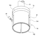
コアドリル74は、例えば、図2~図4に示すように、マウント73に接続された円盤基台740と、円盤基台740の外周から垂下し下端側が解放され上端側が閉鎖された円筒状の円筒基台741とを備えており、円筒基台741の円環状の下端面には、全周にわたって円環状の環状砥石742が配設されている。環状砥石742は、例えば、円筒基台741の先端に砥粒を電着したものとなっている。モータ72によって回転する円筒基台741が、くり抜き送り手段5によってチャックテーブル30に保持された大径ウェーハWに向かって移動させられ、これにより円筒基台741が備える環状砥石742が大径ウェーハWの他方の面Waに切り込み、小径ウェーハW1をくり抜く構成となっている。
As shown in FIGS. 2 to 4, the
また、コアドリル74の円筒基台741の内側では、円筒基台741の下面に、内周側より外周側が下がった傾斜面743が形成されている。傾斜面743は、円錐台の側面の形状をしており、面上に多数の砥粒が電着されて第1の面取り砥石744となっている。モータ72による円筒基台741の回転によって、傾斜面743も同様に回転し、回転する傾斜面743が小径ウェーハW1の第1の角C1に接触しながら、-Z方向に降下することで、小径ウェーハW1の第1の角C1が面取りされることになる。
Further, inside the
円筒基台741には、厚さ方向に貫通する入出口42が、円筒基台741の周方向に等間隔に形成されている。図示の例における入手口42は、Z軸方向に長尺なスリット状であるが、この形状には限定されない。
コアドリル74の外部には、例えば、研削水ノズル40が配設されており、研削水をコアドリル74に向かって噴きつけることができる。噴きつけられた研削水は、円筒基台741が備えるスリット状の入出口42から、円筒基台741の内部に侵入し、内側の傾斜面743を伝って、再び入出口42から円筒基台741の外部へと流れ出る仕組みとなっている。
The
For example, a grinding
図3に示すように、傾斜面743の上部には、例えば、図2に示した研削水ノズル40に替えて、研削水を研削水供給源43から円筒基台741の内側に研削水を供給するための供給口44が備わっていてもよい。供給口44から流入した研削水は、傾斜面743を伝わり、入出口42から排水される。
As shown in FIG. 3, on the upper portion of the
3 ウェーハの製造方法
加工装置1に備えるコアドリル74で、大径ウェーハWをくり抜いて小径ウェーハW1を形成しながら、小径ウェーハW1の第1の角C1の面取りを行い、その後、小径ウェーハW1の第2の角C2の面取りを行うことで強度の高い小径ウェーハW1を製造する。以下に、一連の製造方法を記す。
3 Wafer manufacturing method The
(保護層形成工程)
図5に示すような大径ウェーハWのくり抜き加工や、面取り加工等を行う前に、予め、大径ウェーハWの一方の面Wbと他方の面Waとに、図6に示すように、保護層Rを形成することで、チッピングの発生を防止する。例えば、大径ウェーハWに形成される保護層Rの一例としては、レジスト膜、酸化被膜等が挙げられる。例えば、図示しない酸化装置等によってスチーム酸化や、ドライ酸化等の方法を用いて保護層Rの形成が行われる。
(Protective layer forming process)
Before hollowing out or chamfering the large-diameter wafer W as shown in FIG. 5, one surface Wb and the other surface Wa of the large-diameter wafer W are protected in advance as shown in FIG. By forming the layer R, the occurrence of chipping is prevented. For example, an example of the protective layer R formed on the large-diameter wafer W includes a resist film, an oxide film, and the like. For example, the protective layer R is formed by a method such as steam oxidation or dry oxidation by an oxidizing apparatus (not shown).
(テープ貼着工程)
図7に示すように、上記の保護層形成工程において保護層Rを形成した大径ウェーハWに、図示しない保護テープ貼着手段等を用いて、保護テープTを貼着する。大径ウェーハWに形成された保護層Rに保護テープTの糊層T1が貼着される。そして、保護テープTを介して環状フレームFに大径ウェーハWが支持され、これにより、次工程以降に大径ウェーハWがチャックテーブル30に搬送される際のハンドリング性が向上する。
(Tape application process)
As shown in FIG. 7, the protective tape T is attached to the large-diameter wafer W on which the protective layer R is formed in the protective layer forming step by using a protective tape attaching means (not shown) or the like. The glue layer T1 of the protective tape T is attached to the protective layer R formed on the large-diameter wafer W. Then, the large-diameter wafer W is supported by the annular frame F via the protective tape T, which improves the handleability when the large-diameter wafer W is conveyed to the chuck table 30 in the next step or later.
(保持工程)
図7に示すように、保護テープTが貼着された大径ウェーハWをチャックテーブル30の上に保持する。その際、大径ウェーハWは、環状フレームFが図示しないアーム等により把持されてチャックテーブル30に搬送され、チャックテーブル30の中心と大径ウェーハWの中心とが合致するように載置される。
(Holding process)
As shown in FIG. 7, the large-diameter wafer W to which the protective tape T is attached is held on the chuck table 30. At that time, the large-diameter wafer W is gripped by an arm or the like (not shown) and conveyed to the chuck table 30, and is placed so that the center of the chuck table 30 and the center of the large-diameter wafer W coincide with each other. ..
(くり抜き工程)
図8に示すように、チャックテーブル30に保持された大径ウェーハWに対して、コアドリル74をくり抜き送りすることにより、円筒基台741に備えられた環状砥石742が大径ウェーハWに切り込む。これにより、円筒基台741の環状砥石742が大径ウェーハWをくり抜いて小径ウェーハW1を形成しながら、円筒基台741の内側の傾斜面743が備える第1の面取り砥石744が第1の角C1に当接し、第1の角C1を面取りする。このとき、環状砥石742が保護テープTの糊層T1まで切り込むことで、大径ウェーハWから小径ウェーハW1を完全にくり抜くことができる。
(Cutout process)
As shown in FIG. 8, the
尚、上記のくり抜き工程は、一枚の大径ウェーハWから一枚の小径ウェーハW1をくり抜いてもよいし、一枚の大径ウェーハWから複数の小径ウェーハW1をくり抜いてもよい。一枚の大径ウェーハWから複数の小径ウェーハW1をくり抜く場合、予め、大径ウェーハWの同一円周上に小径ウェーハW1を形成する枚数を定め、その枚数に応じて一枚のくり抜き加工毎に既定の角度だけチャックテーブル30を回転させ、大径ウェーハWの同一円周上に当該枚数の小径ウェーハW1を形成するといった方法が考えられる。 In the above-mentioned hollowing step, one small-diameter wafer W1 may be hollowed out from one large-diameter wafer W, or a plurality of small-diameter wafers W1 may be hollowed out from one large-diameter wafer W. When a plurality of small-diameter wafers W1 are hollowed out from one large-diameter wafer W, the number of small-diameter wafers W1 to be formed on the same circumference of the large-diameter wafer W is determined in advance, and each one of the small-diameter wafers W1 is hollowed out according to the number of small-diameter wafers W1. A method is conceivable in which the chuck table 30 is rotated by a predetermined angle to form the number of small diameter wafers W1 on the same circumference of the large diameter wafer W.
一枚の大径ウェーハWから複数の小径ウェーハW1を形成する加工について、例えば、大径ウェーハWの同一円周上に10枚の小径ウェーハW1を形成したい場合は、一度のくり抜き加工毎にチャックテーブル30を36度ずつ回転させる。つまり、等角度の回転角度を決定する。このとき、チャックテーブル30の回転制御は、例えば、制御手段6が回転のための信号を発信し、それによりモータ311aが駆動して回転部311を鉛直方向の回転軸311bのまわりで回転させることにより行う。そして、36度の回転を行った後、制御手段6が回転停止の信号を発信し、それにより停止部312が回転部311の回転を停止させることでチャックテーブル30の回転を停止させる。その後、大径ウェーハWのくり抜いた場所の隣の部分のくり抜き加工を行うといったような一連の加工が考えられる。
Regarding the processing of forming a plurality of small diameter wafers W1 from one large diameter wafer W, for example, when it is desired to form 10 small diameter wafers W1 on the same circumference of the large diameter wafer W, a chuck is used for each hollowing process. Rotate the table 30 by 36 degrees. That is, the rotation angle of the same angle is determined. At this time, in the rotation control of the chuck table 30, for example, the control means 6 transmits a signal for rotation, whereby the
この加工方法を用いることで、小径ウェーハW1の形成と、形成された小径ウェーハW1の第1の角C1の面取りとを同時に行うことができる。これにより、製造に掛かる時間を短縮することが可能となり、製造の効率が向上する。 By using this processing method, it is possible to simultaneously form the small-diameter wafer W1 and chamfer the first angle C1 of the formed small-diameter wafer W1. This makes it possible to shorten the time required for manufacturing and improve the efficiency of manufacturing.
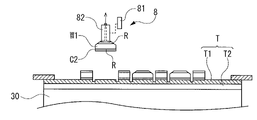
(取得工程)
上記のように、一枚の大径ウェーハWから複数の小径ウェーハW1をくり抜いて形成した後、図9に示すように、くり抜き送り手段5によってコアドリル74を上方へ移動させ、大径ウェーハWから離間させる。その後、図10に示すように、小径ウェーハW1を、ピックアップ装置8を用いて一枚ずつ引き上げて保護テープTから剥離する。このピックアップ装置8は、昇降手段81と、吸引部82とを備えており、吸引部82が発揮する吸引力によって小径ウェーハW1を吸引保持し、吸引部82を昇降手段81によって上昇させ、小径ウェーハW1を引き上げることで、小径ウェーハW1に貼着されていた保護テープTの糊層T1から小径ウェーハW1を引き剥す。
また、環状フレームFだけを支持し、吸引部82が吸引保持する小径ウェーハW1を保護テープTを介して下から突き上げ、糊層T1から小径ウェーハW1を引き剥がしやすくしてもよい。
(Acquisition process)
As described above, after forming a plurality of small-diameter wafers W1 by hollowing out from one large-diameter wafer W, the
Further, the small-diameter wafer W1 that supports only the annular frame F and is suction-held by the
(外形修正工程)
次に、図11に示す外形修正装置9を用いて、取得工程によって取得された各小径ウェーハW1の外形を修正する。この外形修正装置9は、外形修正砥石90と、回転軸91とを備え、図11(a)に示すように、取得された小径ウェーハW1を、ピックアップ装置8の吸引部82と外形修正装置9の回転軸91とで挟持し、図示しないモータ等の動力で回転軸91のまわりに回転させながら、同じく図示しないモータ等で回転する外形修正砥石90を小径ウェーハW1の側面W1cに当接させ、外形の修正を行う。外径の修正には、直径の大きさを修正する直径サイズ修正と、側面に形成された凸凹の粗さを修正する凸凹面修正とがある。外径修正工程では、直径サイズ修正と凸凹面修正との両方の修正を行うか、あるいは、少なくとも一方の修正を行う。
(External shape correction process)
Next, the outer shape of each small diameter wafer W1 acquired in the acquisition step is corrected by using the outer
(第2の面取り工程)
外形の修正を行った後、図11(b)に示すように、第2の面取り工程を行う。上記の外径修正工程と同様に、吸引部82と回転軸91とで小径ウェーハW1を挟持し、吸引部82によって小径ウェーハW1を吸引保持しつつ、小径ウェーハW1を図示しないモータ等の動力で回転軸91のまわりに回転させながら、同じく図示しないモータ等で回転する第2の面取り砥石100を第2の角C2に当接させ、第2の角C2の面取りを行う。第2の面取り砥石100は、その回転軸101を傾けることにより、小径ウェーハW1の第2の角C2と接触して形成する面の形状を調整でき、面取りによって形成される面取りされた部分を所定の大きさや所定の形状にすることができる。
(Second chamfering process)
After modifying the outer shape, a second chamfering step is performed as shown in FIG. 11 (b). Similar to the above outer diameter correction step, the small diameter wafer W1 is sandwiched between the
尚、図12に示すように取得工程の後に、第2の面取り工程を行い、その後外形修正工程を行ってもよい。すなわち、外形修正工程と第2の面取り工程との実施の順番は問わない。 As shown in FIG. 12, after the acquisition step, a second chamfering step may be performed, and then an outer shape correction step may be performed. That is, the order of implementation of the outer shape correction step and the second chamfering step does not matter.
(保護層除去工程)
図13に示すように、小径ウェーハW1の第1の角C1と第2の角C2との両方の面取りが完了した後、剥離液Lを用いて小径ウェーハW1に形成されている保護層Rの除去を行う。その際、例えば、剥離液Lで満たされた専用の容器12等のなかに、保護層Rが形成された小径ウェーハW1を既定時間漬け込むことで小径ウェーハW1に形成されている保護層Rの除去を行う。このとき、剥離液Lは、例えば、濃硫酸と過酸化水素水との混合溶液(SPM)やアンモニアと過酸化水素水との混合溶液(APM)等の溶液が考えられる。
(Protective layer removal process)
As shown in FIG. 13, after chamfering of both the first corner C1 and the second corner C2 of the small diameter wafer W1 is completed, the protective layer R formed on the small diameter wafer W1 using the release liquid L Perform the removal. At that time, for example, the protective layer R formed on the small-diameter wafer W1 is removed by immersing the small-diameter wafer W1 on which the protective layer R is formed in a
1:加工装置 10:ベース 11:コラム A:着脱領域 B:加工領域
2:移動手段 20:ボールネジ 21:ガイドレール 22:モータ
23:可動ブロック 24:保持台
30:チャックテーブル 300:保持面 301:基準面
31:保持手段 310:ケーシング 311:回転部 311a:回転軸
311b:モータ 312:停止部
37:吸引源 39:カバー 391:蛇腹カバー
40:研削水ノズル 42:入出口 43:研削水供給源 44:供給口
5:くり抜き送り手段 50:ボールネジ 51:ガイドレール 52:モータ
53:昇降板 54:ホルダ
6:制御手段
7:くり抜き手段 70:スピンドル 71:ハウジング 72:モータ
73:マウント 74:コアドリル
740:円盤基台 741:円筒基台 742:環状砥石 743:傾斜面
744:第1の面取り砥石
8:ピックアップ装置 81:昇降手段 82:吸引源
9:外形修正装置 90:外形修正砥石 91:回転軸
100:第2の面取り砥石 101:回転軸
12:容器
W:大径ウェーハ Wa:大径ウェーハの他方の面 Wb:大径ウェーハの一方の面
Wc:大径ウェーハの側面 W1:小径ウェーハ W1a:小径ウェーハの他方の面
W1b:小径ウェーハの一方の面 W1c:小径ウェーハの側面
W1d:小径ウェーハの他方の面と側面との稜線
W1e:小径ウェーハの一方の面と側面との稜線
C1:第1の角 C2:第2の角
R:保護層 L:剥離液
T:保護テープ T1:糊層 T2:テープ基台 F:環状フレーム
1: Processing equipment 10: Base 11: Column A: Detachable area B: Processing area 2: Transportation means 20: Ball screw 21: Guide rail 22: Motor
23: Movable block 24: Holding stand
30: Chuck table 300: Holding surface 301: Reference surface
31: Holding means 310: Casing 311: Rotating
9: External shape correction device 90: External shape correction grind 91: Rotating shaft 100: Second chamfering grind 101: Rotating shaft 12: Container W: Large diameter wafer Wa: The other surface of the large diameter wafer Wb: One of the large diameter wafers Surface Wc: Side surface of large diameter wafer W1: Small diameter wafer W1a: The other surface of the small diameter wafer W1b: One surface of the small diameter wafer W1c: Side surface of the small diameter wafer
W1d: Ridge line between the other surface and the side surface of the small diameter wafer
W1e: Ridge line between one surface and the side surface of the small diameter wafer C1: First angle C2: Second angle R: Protective layer L: Stripping liquid
T: Protective tape T1: Glue layer T2: Tape base F: Circular frame
Claims (3)
大径ウェーハの一方の面にテープを貼着するテープ貼着工程と、
該テープを介して大径ウェーハをチャックテーブルで保持する保持工程と、
円筒基台の先端に配設された環状砥石を大径ウェーハの他方の面側から切り込ませ、大径ウェーハから小径ウェーハをくり抜く加工と同時に、該円筒基台の内側に配設された面取り砥石で、小径ウェーハの該他方の面と側面とが接する第1の角を面取りする第1の面取り加工を施す、くり抜き工程と、
該くり抜き工程でくり抜いた小径ウェーハを該テープから剥がす取得工程と、
該取得工程後に、小径ウェーハの該一方の面と該側面とが接する第2の角を面取りする面取り工程と、
からなるウェーハの製造方法。 A wafer manufacturing method for manufacturing small diameter wafers from large diameter wafers.
The tape attachment process of attaching tape to one surface of a large-diameter wafer,
A holding process of holding a large-diameter wafer on a chuck table via the tape,
The annular grindstone arranged at the tip of the cylindrical base is cut from the other surface side of the large diameter wafer, and the small diameter wafer is hollowed out from the large diameter wafer, and at the same time, the chamfer arranged inside the cylindrical base is chamfered. A hollowing process in which a first chamfering process is performed with a grindstone to chamfer the first corner where the other surface and the side surface of the small diameter wafer are in contact with each other.
In the acquisition process of peeling the small diameter wafer hollowed out in the hollowing process from the tape,
After the acquisition step, a chamfering step of chamfering a second corner where the one side of the small diameter wafer and the side surface are in contact with each other.
Wafer manufacturing method consisting of.
該面取り工程後に、該保護層を除去する保護層除去工程と、
を含む請求項1に記載のウェーハの製造方法。 A protective layer forming step of forming a protective layer on one surface and the other surface of the large-diameter wafer before the tape attaching step,
After the chamfering step, a protective layer removing step of removing the protective layer and a step of removing the protective layer
The method for manufacturing a wafer according to claim 1.
Priority Applications (1)
| Application Number | Priority Date | Filing Date | Title |
|---|---|---|---|
| JP2018200919A JP7084845B2 (en) | 2018-10-25 | 2018-10-25 | Wafer manufacturing method |
Applications Claiming Priority (1)
| Application Number | Priority Date | Filing Date | Title |
|---|---|---|---|
| JP2018200919A JP7084845B2 (en) | 2018-10-25 | 2018-10-25 | Wafer manufacturing method |
Publications (2)
| Publication Number | Publication Date |
|---|---|
| JP2020066107A JP2020066107A (en) | 2020-04-30 |
| JP7084845B2 true JP7084845B2 (en) | 2022-06-15 |
Family
ID=70389229
Family Applications (1)
| Application Number | Title | Priority Date | Filing Date |
|---|---|---|---|
| JP2018200919A Active JP7084845B2 (en) | 2018-10-25 | 2018-10-25 | Wafer manufacturing method |
Country Status (1)
| Country | Link |
|---|---|
| JP (1) | JP7084845B2 (en) |
Citations (5)
| Publication number | Priority date | Publication date | Assignee | Title |
|---|---|---|---|---|
| JP2003225818A (en) | 2002-02-04 | 2003-08-12 | Noritake Super Abrasive:Kk | Core drill |
| JP2009142913A (en) | 2007-12-12 | 2009-07-02 | Sumitomo Metal Mining Co Ltd | Wafer bevel machining method, and wheel type rotary grinding wheel |
| JP2011054848A (en) | 2009-09-03 | 2011-03-17 | Disco Abrasive Syst Ltd | Wafer processing method |
| JP2016058623A (en) | 2014-09-11 | 2016-04-21 | 信越半導体株式会社 | Processing method for semiconductor wafer, manufacturing method of bonded wafer, and manufacturing method of epitaxial wafer |
| JP2018014458A (en) | 2016-07-22 | 2018-01-25 | 株式会社ディスコ | Method for manufacturing circular substrate |
Family Cites Families (2)
| Publication number | Priority date | Publication date | Assignee | Title |
|---|---|---|---|---|
| EP0279949A1 (en) * | 1987-02-11 | 1988-08-31 | BBC Brown Boveri AG | Process for manufacturing semiconductor components |
| JP3050632B2 (en) * | 1991-05-13 | 2000-06-12 | 日本インター株式会社 | Method for manufacturing semiconductor device |
-
2018
- 2018-10-25 JP JP2018200919A patent/JP7084845B2/en active Active
Patent Citations (5)
| Publication number | Priority date | Publication date | Assignee | Title |
|---|---|---|---|---|
| JP2003225818A (en) | 2002-02-04 | 2003-08-12 | Noritake Super Abrasive:Kk | Core drill |
| JP2009142913A (en) | 2007-12-12 | 2009-07-02 | Sumitomo Metal Mining Co Ltd | Wafer bevel machining method, and wheel type rotary grinding wheel |
| JP2011054848A (en) | 2009-09-03 | 2011-03-17 | Disco Abrasive Syst Ltd | Wafer processing method |
| JP2016058623A (en) | 2014-09-11 | 2016-04-21 | 信越半導体株式会社 | Processing method for semiconductor wafer, manufacturing method of bonded wafer, and manufacturing method of epitaxial wafer |
| JP2018014458A (en) | 2016-07-22 | 2018-01-25 | 株式会社ディスコ | Method for manufacturing circular substrate |
Also Published As
| Publication number | Publication date |
|---|---|
| JP2020066107A (en) | 2020-04-30 |
Similar Documents
| Publication | Publication Date | Title |
|---|---|---|
| US8021963B2 (en) | Wafer treating method | |
| US10279452B2 (en) | Processing apparatus | |
| TW201904703A (en) | Wafer producing apparatus | |
| JP6920063B2 (en) | How to hold a plate-shaped work | |
| JP2009253244A (en) | Method of carrying out wafer | |
| JP7084845B2 (en) | Wafer manufacturing method | |
| JP2018086693A (en) | Grinding device | |
| TW202224839A (en) | Auxiliary device can be subsequently disposed to a cutting device already delivered to a user | |
| JP6879807B2 (en) | Processing equipment | |
| JP2005028550A (en) | Method for polishing wafer having crystal orientation | |
| JP4966069B2 (en) | Processing equipment | |
| JP7413103B2 (en) | Wafer grinding method | |
| JP2019012773A (en) | Processing method of wafer | |
| JP6125357B2 (en) | Wafer processing method | |
| JP7157624B2 (en) | core drill | |
| JP2017004989A (en) | Manufacturing method for wafer, and manufacturing apparatus of wafer | |
| JP3455907B2 (en) | Semiconductor wafer spin cleaning equipment | |
| US11878387B2 (en) | As-sliced wafer processing method | |
| JP2003211353A (en) | Machining device for wafer | |
| JP2020199596A (en) | Grinding method | |
| JP6422805B2 (en) | Cutting equipment | |
| JP6345981B2 (en) | Support jig | |
| JP2018039070A (en) | Processing method of wafer and grinding device | |
| JP2002254288A (en) | Apparatus and method for finishing work | |
| TW202402460A (en) | Grinding method for workpiece including a rough grinding step, a fine grinding step, and a grinding correction step |
Legal Events
| Date | Code | Title | Description |
|---|---|---|---|
| A621 | Written request for application examination |
Free format text: JAPANESE INTERMEDIATE CODE: A621 Effective date: 20210811 |
|
| A977 | Report on retrieval |
Free format text: JAPANESE INTERMEDIATE CODE: A971007 Effective date: 20220414 |
|
| TRDD | Decision of grant or rejection written | ||
| A01 | Written decision to grant a patent or to grant a registration (utility model) |
Free format text: JAPANESE INTERMEDIATE CODE: A01 Effective date: 20220510 |
|
| A61 | First payment of annual fees (during grant procedure) |
Free format text: JAPANESE INTERMEDIATE CODE: A61 Effective date: 20220603 |
|
| R150 | Certificate of patent or registration of utility model |
Ref document number: 7084845 Country of ref document: JP Free format text: JAPANESE INTERMEDIATE CODE: R150 |