JP7061429B2 - A hard coat film for adhering an inorganic compound layer, and a transparent conductive film and a touch panel using the hard coat film. - Google Patents
A hard coat film for adhering an inorganic compound layer, and a transparent conductive film and a touch panel using the hard coat film. Download PDFInfo
- Publication number
- JP7061429B2 JP7061429B2 JP2016195796A JP2016195796A JP7061429B2 JP 7061429 B2 JP7061429 B2 JP 7061429B2 JP 2016195796 A JP2016195796 A JP 2016195796A JP 2016195796 A JP2016195796 A JP 2016195796A JP 7061429 B2 JP7061429 B2 JP 7061429B2
- Authority
- JP
- Japan
- Prior art keywords
- hard coat
- layer
- film
- hard
- inorganic compound
- Prior art date
- Legal status (The legal status is an assumption and is not a legal conclusion. Google has not performed a legal analysis and makes no representation as to the accuracy of the status listed.)
- Active
Links
Images


Classifications
-
- G—PHYSICS
- G02—OPTICS
- G02B—OPTICAL ELEMENTS, SYSTEMS OR APPARATUS
- G02B1/00—Optical elements characterised by the material of which they are made; Optical coatings for optical elements
- G02B1/10—Optical coatings produced by application to, or surface treatment of, optical elements
-
- B—PERFORMING OPERATIONS; TRANSPORTING
- B32—LAYERED PRODUCTS
- B32B—LAYERED PRODUCTS, i.e. PRODUCTS BUILT-UP OF STRATA OF FLAT OR NON-FLAT, e.g. CELLULAR OR HONEYCOMB, FORM
- B32B27/00—Layered products comprising a layer of synthetic resin
- B32B27/18—Layered products comprising a layer of synthetic resin characterised by the use of special additives
- B32B27/20—Layered products comprising a layer of synthetic resin characterised by the use of special additives using fillers, pigments, thixotroping agents
-
- B—PERFORMING OPERATIONS; TRANSPORTING
- B32—LAYERED PRODUCTS
- B32B—LAYERED PRODUCTS, i.e. PRODUCTS BUILT-UP OF STRATA OF FLAT OR NON-FLAT, e.g. CELLULAR OR HONEYCOMB, FORM
- B32B27/00—Layered products comprising a layer of synthetic resin
-
- B—PERFORMING OPERATIONS; TRANSPORTING
- B32—LAYERED PRODUCTS
- B32B—LAYERED PRODUCTS, i.e. PRODUCTS BUILT-UP OF STRATA OF FLAT OR NON-FLAT, e.g. CELLULAR OR HONEYCOMB, FORM
- B32B5/00—Layered products characterised by the non- homogeneity or physical structure, i.e. comprising a fibrous, filamentary, particulate or foam layer; Layered products characterised by having a layer differing constitutionally or physically in different parts
- B32B5/18—Layered products characterised by the non- homogeneity or physical structure, i.e. comprising a fibrous, filamentary, particulate or foam layer; Layered products characterised by having a layer differing constitutionally or physically in different parts characterised by features of a layer of foamed material
-
- B—PERFORMING OPERATIONS; TRANSPORTING
- B32—LAYERED PRODUCTS
- B32B—LAYERED PRODUCTS, i.e. PRODUCTS BUILT-UP OF STRATA OF FLAT OR NON-FLAT, e.g. CELLULAR OR HONEYCOMB, FORM
- B32B7/00—Layered products characterised by the relation between layers; Layered products characterised by the relative orientation of features between layers, or by the relative values of a measurable parameter between layers, i.e. products comprising layers having different physical, chemical or physicochemical properties; Layered products characterised by the interconnection of layers
- B32B7/04—Interconnection of layers
- B32B7/06—Interconnection of layers permitting easy separation
-
- B—PERFORMING OPERATIONS; TRANSPORTING
- B32—LAYERED PRODUCTS
- B32B—LAYERED PRODUCTS, i.e. PRODUCTS BUILT-UP OF STRATA OF FLAT OR NON-FLAT, e.g. CELLULAR OR HONEYCOMB, FORM
- B32B9/00—Layered products comprising a layer of a particular substance not covered by groups B32B11/00 - B32B29/00
-
- B—PERFORMING OPERATIONS; TRANSPORTING
- B32—LAYERED PRODUCTS
- B32B—LAYERED PRODUCTS, i.e. PRODUCTS BUILT-UP OF STRATA OF FLAT OR NON-FLAT, e.g. CELLULAR OR HONEYCOMB, FORM
- B32B9/00—Layered products comprising a layer of a particular substance not covered by groups B32B11/00 - B32B29/00
- B32B9/04—Layered products comprising a layer of a particular substance not covered by groups B32B11/00 - B32B29/00 comprising such particular substance as the main or only constituent of a layer, which is next to another layer of the same or of a different material
- B32B9/045—Layered products comprising a layer of a particular substance not covered by groups B32B11/00 - B32B29/00 comprising such particular substance as the main or only constituent of a layer, which is next to another layer of the same or of a different material of synthetic resin
-
- B—PERFORMING OPERATIONS; TRANSPORTING
- B32—LAYERED PRODUCTS
- B32B—LAYERED PRODUCTS, i.e. PRODUCTS BUILT-UP OF STRATA OF FLAT OR NON-FLAT, e.g. CELLULAR OR HONEYCOMB, FORM
- B32B2307/00—Properties of the layers or laminate
- B32B2307/20—Properties of the layers or laminate having particular electrical or magnetic properties, e.g. piezoelectric
- B32B2307/202—Conductive
-
- B—PERFORMING OPERATIONS; TRANSPORTING
- B32—LAYERED PRODUCTS
- B32B—LAYERED PRODUCTS, i.e. PRODUCTS BUILT-UP OF STRATA OF FLAT OR NON-FLAT, e.g. CELLULAR OR HONEYCOMB, FORM
- B32B2307/00—Properties of the layers or laminate
- B32B2307/40—Properties of the layers or laminate having particular optical properties
- B32B2307/412—Transparent
-
- B—PERFORMING OPERATIONS; TRANSPORTING
- B32—LAYERED PRODUCTS
- B32B—LAYERED PRODUCTS, i.e. PRODUCTS BUILT-UP OF STRATA OF FLAT OR NON-FLAT, e.g. CELLULAR OR HONEYCOMB, FORM
- B32B2307/00—Properties of the layers or laminate
- B32B2307/50—Properties of the layers or laminate having particular mechanical properties
- B32B2307/546—Flexural strength; Flexion stiffness
-
- B—PERFORMING OPERATIONS; TRANSPORTING
- B32—LAYERED PRODUCTS
- B32B—LAYERED PRODUCTS, i.e. PRODUCTS BUILT-UP OF STRATA OF FLAT OR NON-FLAT, e.g. CELLULAR OR HONEYCOMB, FORM
- B32B2307/00—Properties of the layers or laminate
- B32B2307/70—Other properties
- B32B2307/724—Permeability to gases, adsorption
- B32B2307/7242—Non-permeable
-
- B—PERFORMING OPERATIONS; TRANSPORTING
- B32—LAYERED PRODUCTS
- B32B—LAYERED PRODUCTS, i.e. PRODUCTS BUILT-UP OF STRATA OF FLAT OR NON-FLAT, e.g. CELLULAR OR HONEYCOMB, FORM
- B32B2457/00—Electrical equipment
- B32B2457/20—Displays, e.g. liquid crystal displays, plasma displays
- B32B2457/208—Touch screens
Description
本発明は、電極フィルム、ガスバリアフィルム等に好適な、無機化合物層を接着するためのハードコート層を有するハードコートフィルムに関する。 The present invention relates to a hard coat film having a hard coat layer for adhering an inorganic compound layer, which is suitable for an electrode film, a gas barrier film and the like.
タッチパネルに用いる電極フィルムは、透明基材の表面に積層されたハードコート層上にスパッタリング法によりITO(スズドープ酸化インジウム)を成膜し、ITO膜にエッチングにより電極パターンを形成することにより作成される。
特許文献1は、ハードコート層にITOのような透明導電層を形成した場合に、これらの層が良好な接着性を有するハードコートフィルムの技術を開示している。
ところが、ハードコート層にITOを成膜した電極フィルムでは、ITO膜が存在する部分とITOが除去された部分とに光学特性(透過率、色相、反射率など)の差が生じ、電極パターンが見えてしまう現象が発生し、見栄えが悪くなる。そのため、近年、電極フィルムは、光学特性を調整する光学調整層をハードコート層とITO膜との間に配置する構成をとるようになった。これにより、ITO膜が存在する部分における光学特性と、ITO膜が除去され光学調整層が露出した部分における光学特性との差が小さくなり電極パターンが目立たなくなる。
The electrode film used for the touch panel is created by forming an ITO (tin-doped indium oxide) film on the hard coat layer laminated on the surface of the transparent substrate by a sputtering method and forming an electrode pattern on the ITO film by etching. ..
However, in the electrode film in which ITO is formed on the hard coat layer, the optical characteristics (transmittance, hue, reflectance, etc.) differ between the portion where the ITO film is present and the portion where ITO is removed, resulting in an electrode pattern. A phenomenon that makes it visible occurs, and the appearance becomes poor. Therefore, in recent years, the electrode film has come to have a structure in which an optical adjustment layer for adjusting optical characteristics is arranged between a hard coat layer and an ITO film. As a result, the difference between the optical characteristics in the portion where the ITO film is present and the optical characteristics in the portion where the ITO film is removed and the optical adjustment layer is exposed becomes small, and the electrode pattern becomes inconspicuous.
上述のようにハードコート層とITO膜との間に光学調整層を有する電極フィルムでは、ハードコート層の上に光学調整層をスパッタリング法により成膜するため、光学調整層との接着性がよいハードコート層を有するフィルムが必要である。特に、電極フィルムの信頼性を高めるために、経時での変化が少なく、光学調整層との接着性が良好に維持されることが望まれる。 As described above, in the electrode film having an optical adjustment layer between the hard coat layer and the ITO film, the optical adjustment layer is formed on the hard coat layer by a sputtering method, so that the adhesiveness with the optical adjustment layer is good. A film with a hard coat layer is required. In particular, in order to improve the reliability of the electrode film, it is desired that the change with time is small and the adhesiveness with the optical adjustment layer is well maintained.
特許文献1は、ハードコート層に所定の疎水化シリカゲルおよび特定のレベリング剤を配合することにより、ハードコート層とITOとの良好な接着性に関して開示しているが、光学調整層との接着性に関しては開示も示唆もしていない。
そこで、本発明は、無機化合物層との接着性を向上したハードコート層を有するハードコートフィルム(以下、「ハードコートフィルム」)の提供を目的とする。特に、経時での変化が少なく、接着性が良好に維持されるハードコートフィルムの提供を目的とする。 Therefore, an object of the present invention is to provide a hard coat film (hereinafter, "hard coat film") having a hard coat layer having improved adhesiveness to the inorganic compound layer. In particular, it is an object of the present invention to provide a hard-coated film that does not change with time and maintains good adhesiveness.
本発明のハードコートフィルムは、ハードコート層上に無機化合物層が接着される。ハードコート層は反応性を有するように修飾された粒子とバインダー樹脂とを含み、前記粒子の含有量が前記バインダー樹脂固形分の100重量部に対して1重量部以上60重量部以下である。 In the hard coat film of the present invention, an inorganic compound layer is adhered on the hard coat layer. The hardcoat layer contains particles modified to have reactivity and a binder resin, and the content of the particles is 1 part by weight or more and 60 parts by weight or less with respect to 100 parts by weight of the solid content of the binder resin.
また、本発明のハードコートフィルムは、好適には、前記粒子の平均粒子径が100nm以上1000nm以下である。 Further, in the hard coat film of the present invention, the average particle diameter of the particles is preferably 100 nm or more and 1000 nm or less.
また、本発明のハードコートフィルムは、好適には、前記粒子が一次粒子の凝集体として二次粒子を構成する場合、前記一次粒子の径が1nm以上100nm以下である。 Further, in the hard coat film of the present invention, preferably, when the particles form secondary particles as aggregates of primary particles, the diameter of the primary particles is 1 nm or more and 100 nm or less.
また、本発明のハードコートフィルムは、好適には、前記粒子が、シリカ、アルミナ、チタン、ジルコニア、炭酸カルシウム、炭酸マグネシウム、硫酸バリウム、またはこれらの2以上の組み合わせである。 Further, in the hard coat film of the present invention, the particles are preferably silica, alumina, titanium, zirconia, calcium carbonate, magnesium carbonate, barium sulfate, or a combination of two or more thereof.
また、本発明のハードコートフィルムは、好適には、前記粒子が、アクリロイル基、水酸基、カルボキシル基、アミノ基、エポキシ基、イソシアネート基、またはこれらの官能基の2以上の組み合わせを有する。 Further, in the hard coat film of the present invention, the particles preferably have an acryloyl group, a hydroxyl group, a carboxyl group, an amino group, an epoxy group, an isocyanate group, or a combination of two or more of these functional groups.
また、本発明のハードコートフィルムは、好適には、JIS-K5600-5-1(1999)に準拠した円筒形マンドレル法で測定した前記ハードコート層の耐屈曲試験の値が6mm以下である。 Further, in the hard coat film of the present invention, the value of the bending resistance test of the hard coat layer measured by the cylindrical mandrel method according to JIS-K5600-5-1 (1999) is preferably 6 mm or less.
また、本発明のハードコートフィルムは、好適には、前記フィルムに無機化合物層を積層し、煮沸処理した後の砂時計クロスカット剥離試験で、無機化合物層がハードコート層から部分的にしか剥がれていないまたはそれより良好である。 Further, in the hard coat film of the present invention, preferably, in the hourglass cross-cut peeling test after laminating the inorganic compound layer on the film and boiling the film, the inorganic compound layer is only partially peeled off from the hard coat layer. No or better than that.
また、本発明のハードコートフィルムは、好適には、前記無機化合物層が光学調整層またはガスバリア層である。 Further, in the hard coat film of the present invention, the inorganic compound layer is preferably an optical adjustment layer or a gas barrier layer.
また、本発明のハードコートフィルムは、好適には、前記無機化合物がSiO2またはNb2Ox(但し4≦x≦5)である。 Further, in the hard coat film of the present invention, the inorganic compound is preferably SiO 2 or Nb 2 Ox (provided that 4 ≦ x ≦ 5).
また、本発明のハードコートフィルムは、好適には、前記無機化合物層が単層または多層で構成される。 Further, in the hard coat film of the present invention, the inorganic compound layer is preferably composed of a single layer or multiple layers.
また、本発明の透明導電性フィルムは、上述した本発明のハードコートフィルムを用いたことを特徴とする。 Further, the transparent conductive film of the present invention is characterized in that the above-mentioned hard coat film of the present invention is used.
また、本発明のタッチパネルは、上述した本発明のハードコートフィルムを使用したことを特徴とする。 Further, the touch panel of the present invention is characterized in that the above-mentioned hard coat film of the present invention is used.
本発明によれば、無機化合物層とハードコート層との接着性が向上できる。特に、経時での変化が少なく、接着性が良好に維持される。 According to the present invention, the adhesiveness between the inorganic compound layer and the hard coat layer can be improved. In particular, there is little change over time and good adhesiveness is maintained.
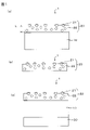
以下、図1から5を参照して、本発明の、無機化合物層40を接着するためのハードコートフィルム1の実施の形態について説明する。なお、無機化合物層40は、無機化合物を有する層であれば、無機化合物を含む層の場合でも、無機化合物それ自体の層の場合でもよい。
Hereinafter, embodiments of the
本発明のハードコートフィルム1は、ハードコート層20を有し、ハードコート層20が反応性を有するように修飾された粒子(反応性修飾粒子)21とバインダー樹脂22とを含み、反応性修飾粒子21の含有量がバインダー樹脂22の100重量部に対して1重量部以上60重量部以下であることを特徴とする。
The
本発明の実施形態は、基本的な構成として、図1(a)に示すように、支持体10と支持体10の上に形成されたハードコート層20とを備える。ハードコートフィルム1は、図1(a)に示すものだけでなく、ハードコート層単層のフィルム(図1(b))であってもよいし、支持体10の、ハードコート層20が形成された面とは反対側の面にバックコート層(図1(c))を備えていてもよい。
As a basic configuration, an embodiment of the present invention includes a
このようなハードコートフィルム1は、図2に示すように、無機化合物層40がハードコート層20上に積層される。この時、ハードコート層20は無機化合物層40に対して優れた接着性を有する。
In such a
まず、ハードコート層20を構成する反応性修飾粒子21とバインダー樹脂22とについて説明する。
First, the
バインダー樹脂22は、後述する反応性修飾粒子21のバインダーとしての機能を有する。バインダー樹脂22は反応性官能基を有することが望ましい。その場合、反応性修飾粒子21の反応性官能基と結合し、反応性修飾粒子21の脱落を効果的に防止する事が出来る。バインダー樹脂22の反応性官能基としては、アクリロイル基、水酸基、カルボキシル基、アミノ基、エポキシ基、イソシアネート基等が挙げられる。
The
バインダー樹脂22としては、電離放射線硬化性樹脂、熱硬化性樹脂、熱可塑性樹脂等の樹脂を単独又は2以上組み合わせる事ができ、目的に応じて使い分ける事ができる。中でもより優れた硬度が必要な場合は電離放射線硬化樹脂を使用することが好ましい。
As the
電離放射線硬化性樹脂としては、電離放射線(紫外線または電子線)の照射により架橋硬化することができる樹脂を挙げることができ、例えば、1分子中に1又は2個以上の(メタ)アクリロイル基を有するアクリル樹脂が特に好ましく使用される。このアクリル系化合物としては、ウレタン(メタ)アクリレート、ポリエステル(メタ)アクリレート、エポキシ(メタ)アクリレート、メラミン(メタ)アクリレート、ポリフルオロアルキル(メタ)アクリレート、シリコーン(メタ)アクリレート等を挙げることができる。 Examples of the ionizing radiation curable resin include resins that can be crosslinked and cured by irradiation with ionizing radiation (ultraviolet rays or electron beams), and for example, one or two or more (meth) acryloyl groups in one molecule. Acryloyl resin having is particularly preferably used. Examples of the acrylic compound include urethane (meth) acrylate, polyester (meth) acrylate, epoxy (meth) acrylate, melamine (meth) acrylate, polyfluoroalkyl (meth) acrylate, silicone (meth) acrylate and the like. ..
熱硬化性樹脂としては、例えば、ポリエステルアクリレート系樹脂、ポリウレタンアクリレート系樹脂、エポキシアクリレート系樹脂、エポキシ系樹脂、メラミン系樹脂、フェノール系樹脂、シリコーン系樹脂などが挙げられる。 Examples of the thermosetting resin include polyester acrylate resin, polyurethane acrylate resin, epoxy acrylate resin, epoxy resin, melamine resin, phenol resin, silicone resin and the like.
熱可塑性樹脂としては、例えば、ポリエステル系樹脂、アクリル系樹脂、ポリカーボネート系樹脂、セルロース系樹脂、アセタール系樹脂、ビニル系樹脂、ポリエチレン系樹脂、ポリスチレン系樹脂、ポリプロピレン系樹脂、ポリアミド系樹脂、ポリイミド系樹脂、フッ素系樹脂などが挙げられる。 Examples of the thermoplastic resin include polyester resin, acrylic resin, polycarbonate resin, cellulose resin, acetal resin, vinyl resin, polyethylene resin, polystyrene resin, polypropylene resin, polyamide resin, and polyimide resin. Examples include resins and fluororesins.
また、バインダー樹脂22は、高分子量樹脂を一定量含むことが、より好ましい。高分子量樹脂と後述する反応性修飾粒子21とを組み合わせることで、ハードコート層20に、硬度を損なうことなく、ある程度の柔軟性を付与することができ、ハードコート層20に対する無機化合物層40のアンカー効果が高まる。これにより、ハードコート層20と無機化合物層40の接着性がより向上する。
高分子量樹脂とは、重量平均分子量(Mw)が10000以上の樹脂であり、好ましくは10000~150000、より好ましくは30000~100000である。
高分子量樹脂としては、電離放射線硬化性樹脂、熱硬化性樹脂、熱可塑性樹脂等の樹脂を単独又は2以上を組み合わせる事ができる。電離放射線硬化性樹脂、熱硬化性樹脂、熱可塑性樹脂の例としては、バインダー樹脂22の電離放射線硬化性樹脂、熱硬化性樹脂、熱可塑性樹脂の例として上記に列挙したものと同様である。
含有量としては、バインダー樹脂22(固形分)100重量部に対して、1重量部以上50重量部以下、より好ましくは5重量部以上40重量部以下である。なお、バインダー樹脂22が高分子量樹脂を含む場合、「バインダー樹脂22(固形分)」とは、高分子量樹脂を含んだバインダー樹脂22全体の固形分をいう。
Further, it is more preferable that the
The high molecular weight resin is a resin having a weight average molecular weight (Mw) of 10,000 or more, preferably 10,000 to 150,000, and more preferably 30,000 to 100,000.
As the high molecular weight resin, resins such as ionizing radiation curable resin, thermosetting resin, and thermoplastic resin can be used alone or in combination of two or more. Examples of the ionizing radiation curable resin, the thermosetting resin, and the thermoplastic resin are the same as those listed above as examples of the ionizing radiation curable resin, the thermosetting resin, and the thermoplastic resin of the
The content is 1 part by weight or more and 50 parts by weight or less, more preferably 5 parts by weight or more and 40 parts by weight or less with respect to 100 parts by weight of the binder resin 22 (solid content). When the
反応性修飾粒子21は、ハードコート層20の無機化合物層40に対する接着性の向上、及び経時での接着性の維持に寄与する。
反応性修飾粒子21は、無機系粒子の表面を修飾処理することにより、無機系粒子の表面に反応性官能基が付与された粒子である。反応性官能基はバインダー樹脂22の反応性官能基と結合することにより、反応性修飾粒子21のハードコート層20からの脱落を防止する。また、反応性官能基を有することにより高温多湿状態でも無機化合物層との接着性を維持することが出来ると推察される。
無機系粒子の一例として、シリカ、アルミナ、チタン、ジルコニア、炭酸カルシウム、炭酸マグネシウム、硫酸バリウム等があげられ、これら無機系粒子を単独又は2以上組み合わせて使用することが出来る。反応性官能基としては、例えばアクリロイル基、水酸基、カルボキシル基、アミノ基、エポキシ基、イソシアネート基等を例示することができ、単独およびこれらの反応性官能基の2以上を組み合わせて使用することが出来る。
The reactive modified
The reactive modified
Examples of the inorganic particles include silica, alumina, titanium, zirconia, calcium carbonate, magnesium carbonate, barium sulfate and the like, and these inorganic particles can be used alone or in combination of two or more. Examples of the reactive functional group include an acryloyl group, a hydroxyl group, a carboxyl group, an amino group, an epoxy group, an isocyanate group and the like, and they can be used alone or in combination of two or more of these reactive functional groups. I can.
反応性修飾粒子21の含有量は、無機化合物層40への接着性を発揮させるために、反応性修飾粒子21の下限値がバインダー樹脂22(固形分)の100重量部に対して1重量部以上、好ましくは3重量部以上、より好ましくは5重量部以上、もっとも好ましくは10重量部以上である。一方、反応性修飾粒子21の上限値は特に決まっていないが、バインダー樹脂22(固形分)の100重量部に対して60重量部以下、好ましくは40重量部以下、より好ましくは30重量部以下である。
反応性修飾粒子21の含有量が上述した範囲より少ない場合は、無機化合物層40との接着性が弱くなりやすい。一方、上述した範囲より多い場合は、透明性を保つことが困難となり好ましくない。
The content of the reactive modified
When the content of the reactive modified
反応性修飾粒子21は、所定の大きさであれば、一次粒子でも凝集体である二次粒子であってもかまわないが、より接着性を得る為には、二次粒子の方が好ましい。一次粒子の凝集体である二次粒子を反応性修飾粒子21として使用した場合、単に同等の大きさの一次粒子を使用した場合よりも、接着性が向上する理由については、はっきりとしていないが、表面に突出した粒子の無機化合物層40との接触面積が増える為ではないかと考えられる。
反応性修飾粒子21の平均粒子径(一次粒子又は一次粒子からなる凝集体としての二次粒子を含む)は、ハードコート層20の厚みによって異なるため、一概には言えないが、下限値が100nm以上、好ましくは、110nm以上、より好ましくは、130nm以上である。また上限値が、1000nm以下、好ましくは、800nm以下、より好ましくは、600nm以下である。さらに上記の内、反応性修飾粒子21が一次粒子の凝集体としての二次粒子で構成される場合、その二次粒子の構成物である一次粒子の平均粒子径は、下限値が1nm以上、好ましくは、20nm以上、より好ましくは、30nm以上である。また上限値が、100nm以下、好ましくは、80nm以下、より好ましくは、60nm以下である。
反応性修飾粒子21の平均粒子径あるいは反応性修飾粒子21が二次粒子で構成される場合は一次粒子の平均粒子径を上述した下限値以上とすることにより、無機化合物層40に対する接着性を得ることができる。一方、これらの平均粒子径をそれぞれ上述した上限値以下とすることにより、透明用途に使用できる光透過性を得ることができる。
なお、粒子の平均粒子径はレーザー回析・散乱法により測定できる体積平均粒子径(D50)の値を指す。
The reactive modified
The average particle size of the reactive modified particles 21 (including the primary particles or the secondary particles as aggregates composed of the primary particles) varies depending on the thickness of the
The average particle size of the reactive modified
The average particle size of the particles refers to the value of the volume average particle size (D50) that can be measured by the laser diffraction / scattering method.
ハードコート層20中には、さらに硬化方法に応じて、光開始剤、硬化剤等を含んでいてもよい。
光開始剤としては、アセトフェノン類、ベンゾフェノン類、ミヒラーケトン、ベンゾイン、ベンジルメチルケタール、ベンゾイルベンゾエート、α-アシルオキシムエステル、チオキサンソン類などの光ラジカル重合開始剤や、オニウム塩類、スルホン酸エステル、有機金属錯体などの光カチオン重合開始剤が挙げられる。
また、硬化剤としては、ポリイソシアネート、アミノ樹脂、エポキシ樹脂、カルボン酸などの化合物を、適合する樹脂に合わせて適宜使用することができる。
The
Examples of the photoinitiator include photoradical polymerization initiators such as acetophenones, benzophenones, Michler ketone, benzoin, benzylmethyl ketal, benzoylbenzoate, α-acyloxime ester, and thioxanthones, onium salts, sulfonic acid esters, and organic metal complexes. Examples thereof include photocationic polymerization initiators such as.
Further, as the curing agent, compounds such as polyisocyanate, amino resin, epoxy resin, and carboxylic acid can be appropriately used according to the compatible resin.
ハードコート層20中には、性能を阻害しない範囲内で、上述したバインダー樹脂、高分子樹脂、反応性修飾粒子、光開始剤、硬化剤の他に、帯電防止剤、分散剤、凝集剤、紫外線吸収剤、酸化防止剤、レベリング剤などの添加剤をさらに含んでいてもよい。
In the
ハードコート層20の厚み(図1(a)のL参照)は、ハードコートフィルム1が支持体10を備える場合は、0.1~10.0μm、好ましくは0.5~5.0μm、より好ましくは1.0~3.0μmである。また、ハードコートフィルム1が支持体10に加えてバックコート層30も備える場合は、0.1~10.0μm、好ましくは1.0~5.0μm、より好ましくは1.0~3.0μmである。このような厚みを有することにより、ハードコート層20と無機化合物層40との接着性が改善する。
なお、ハードコート層単層の場合は、その厚みが0.1~10.0μm、好ましくは0.5~5.0μm、より好ましくは1.0~3.0μmである。厚みを0.1μ以上とすることにより、無機化合物層40との接着性を有しながら、塗膜強度を十分なものとし、また、ハンドリング性を良好なものとする。
ハードコート層20の厚みは反射分光膜厚計(大塚電子 FE-300)を用いて測定される。
The thickness of the hard coat layer 20 (see L in FIG. 1A) is 0.1 to 10.0 μm, preferably 0.5 to 5.0 μm, when the
In the case of a hard coat layer single layer, the thickness thereof is 0.1 to 10.0 μm, preferably 0.5 to 5.0 μm, and more preferably 1.0 to 3.0 μm. By setting the thickness to 0.1 μm or more, the coating film strength is sufficient and the handleability is good while having adhesiveness to the
The thickness of the
次に、ハードコートフィルム1が支持体10を有する場合の支持体10について説明する。支持体10は光学的透明性の高いプラスチックフィルムであれば特に制限されることなく使用することができる。例えば、ポリエチレンテレフタレート、ポリブチレンテレフタレート、ポリエチレンナフタレート、ポリカーボネート、ポリシクロオレフィン、ポリエチレン、ポリカーボネート、ポリプロピレン、ポリスチレン、トリアセチルセルロース、アクリル、ポリ塩化ビニル、ノルボルネン化合物等が使用できる。このうち、延伸加工、特に二軸延伸加工されたポリエチレンテレフタレートフィルムが、機械的強度や寸法安定性に優れる点で好ましい。また、ハードコート層20との接着性を向上させるために、表面にコロナ放電処理を施したり、易接着層を設けたものも好適に用いられる。なお、支持体10の厚みは、通常6~250μ程度であることが好ましく、より好ましくは23~188μm程度である。
支持体10は、光透過性あることが好ましく、具体的には、全光線透過率(JISK7136)として85%以上、好適には90%以上である。
Next, the
The
また、ハードコートフィルム1は、上述のように、支持体10のハードコート層20とは反対の面にバックコート層30(図1(c))をさらに備えても良い。
その場合、バックコート層30は特に限定されないが、ハードコート層、粘着層、帯電防止層等から選ぶ事ができ、また上述のハードコート層20を備えても良い。
Further, as described above, the
In that case, the
ハードコートフィルム1の作製方法は特に限定されないが、例えば、支持体10を有する場合、上述したハードコート層20の材料を適当な溶媒に溶解または分散させたハードコート層用塗布液を、バーコーティングのような公知の方法で支持体上に塗布し、乾燥し、必要に応じて紫外線照射して、作製できる。また、あらかじめ支持体10上に離型層を形成しておくことで、ハードコート層20を支持体10上に形成したのち、当該支持体10を剥離除去することで、ハードコート層単層からなるフィルムとすることができる。また、バックコート層30を有するハードコートフィルム1の場合は、ハードコート層20を備えた支持体10のハードコート層20とは反対側の面に、適当な溶媒に溶解または分散させたバックコート層用塗布液上を、バーコーティングのような公知の方法で塗布し、乾燥し、必要に応じて紫外線照射して、作製できる。
The method for producing the
次に、ハードコート層20の特性について説明する。ハードコート層20が備えるべき特性は、接着性および柔軟性である。
Next, the characteristics of the
まず、接着性は、例えば、無機化合物層を積層して何も処理していない状態(以下、「初期接着性試験」という)と促進耐候性試験である煮沸処理を行った後の状態(以下、「煮沸後接着性試験」という)の2種類の状態で砂時計クロスカット剥離試験を行い、その結果によって優劣の判定を行い評価することができる。砂時計クロスカット剥離試験は、後述するように、無機化合物層40の表面を砂時計のような形状にクロスカットして剥離を行うため、碁盤目状にクロスカットするよりも過酷な条件下で接着性の優劣が評価できる。
First, the adhesiveness is, for example, a state in which an inorganic compound layer is laminated and nothing is treated (hereinafter referred to as "initial adhesiveness test") and a state after boiling treatment which is an accelerated weather resistance test (hereinafter referred to as "initial adhesiveness test"). , "Post-boiling adhesiveness test"), an hourglass cross-cut peeling test can be performed, and the superiority or inferiority can be determined and evaluated based on the results. As will be described later, in the hourglass cross-cut peeling test, the surface of the
ここで、初期接着性試験方法(砂時計クロスカット剥離試験方法)は、次の通りである。 Here, the initial adhesiveness test method (hourglass cross-cut peeling test method) is as follows.
ハードコートフィルム1に無機化合物(例えば、SiO2、Nb2Ox(但し、4≦x≦5)等)をスパッタし、厚み約200nmの無機化合物層40を成膜した試験片を作製する(試験片作製工程)。
Inorganic compounds (for example, SiO 2 , Nb 2 Ox (however, 4 ≦ x ≦ 5), etc.) are sputtered on the hard-coated
次いで、図3に示すように、線分DD´および線分EE´が平行であって、これらの線分の間の幅が2cmになるように、無機化合物層40の表面に切れ込みを入れる。次に、線分FF´および線分GG´が互いに交差し、線分FF´およびGG´の一端部がそれぞれ線分DD´に交わり、線分FF´およびGG´の他端部がそれぞれ線分EE´に交わるように、無機化合物層40の表面に切れ込みを入れる。この時、線分DD´、EE´、FF´およびGG´により形成される二つの三角形ABCおよびAB´C´が、頂角30度かつ高さ1cmの二等辺三角形となるように切れ込みを入れる。ここで、線分FF´および線分GG´が交差する点を頂点Aとし、線分DD´上の線分GG´および線分FF´の交点をそれぞれ点Bと点Cとし、線分EE´上の線分GG´および線分FF´の交点をそれぞれ点B´と点C´とする(切り込み工程)。
Next, as shown in FIG. 3, a notch is made in the surface of the
切り込みを入れた二つの二等辺三角形を覆うように、粘着テープ(ニチバン社製、セロテープ(登録商標))を接着させ、接着した粘着テープを所定の角度および速さで引き離す(1回目の剥離)。ついで、1回目剥離後の試験片に、新しく用意した粘着テープを用いて、1回目の剥離を行った同一場所にて、再度同様に剥離試験を行う(2回目の剥離)。なお、上述した切り込みの仕方および連続して同一場所に2回の剥離を行う以外はJISK5600-5-6に規定されているクロスカット法に準拠して行う(剥離工程)。 Adhesive tape (Nichiban Co., Ltd., cellophane tape (registered trademark)) is adhered so as to cover the two isosceles triangles with cuts, and the adhered adhesive tape is pulled apart at a predetermined angle and speed (first peeling). .. Then, using a newly prepared adhesive tape on the test piece after the first peeling, the same peeling test is performed again at the same place where the first peeling was performed (second peeling). In addition, except for the above-mentioned cutting method and continuous peeling at the same place twice, the cross-cut method specified in JIS K5600-5-6 is used (peeling step).
初期接着性試験方法に従って試験して、本発明においては、ハードコート層の接着性は、2回目の剥離において、無機化合物層40がハードコート層20から全く剥がれていないものが好ましい。このような接着性を有することにより、無機化合物層40への経時での接着性が向上する。
Tested according to the initial adhesiveness test method, in the present invention, the adhesiveness of the hard coat layer is preferably such that the
また、煮沸後接着性試験方法は、上記に説明した初期接着性試験方法における試験片作製工程後、切り込み工程前に、試験片作製工程で得られた試験片を所定の時間にて純水を用いて煮沸処理する工程(煮沸処理工程)を有する点が初期接着性試験方法と異なる。
なお、煮沸処理工程は、無機化合物層40がSiO2の場合は6時間煮沸する。また、無機化合物層40がNb2Ox(但し、4≦x≦5)の場合は1時間煮沸する。
Further, in the post-boiling adhesiveness test method, after the test piece manufacturing step in the initial adhesiveness test method described above and before the cutting step, the test piece obtained in the test piece manufacturing step is subjected to pure water at a predetermined time. It differs from the initial adhesiveness test method in that it has a step of boiling treatment using it (boiling treatment step).
In the boiling treatment step, when the
煮沸後接着性試験方法に従って試験して、本発明においては、ハードコート層の接着性は、1回目または2回目の剥離において、無機化合物層40がハードコート層20から部分的にしか剥がれていないまたはそれより良好なものが好ましく、1回目または2回目の剥離において、無機化合物層40がハードコート層20から部分的にしか剥がれていないものより良好なものがより好ましく、2回目の剥離において、無機化合物層40がハードコート層20から全く剥がれていないものがさらに好ましい。
このような接着性を有することにより、高温多湿下での無機化合物層40への接着性が向上する。
Tested according to the post-boiling adhesiveness test method, in the present invention, the adhesiveness of the hardcourt layer is such that the
By having such adhesiveness, the adhesiveness to the
あるいは、初期接着性試験および煮沸後接着性試験法を合わせた場合、本発明においては、ハードコート層20の接着性は、初期接着性試験の2回目の剥離にて無機化合物層40がハードコート層20から全く剥がれていないものかつ煮沸後接着性試験の1回目剥離にて無機化合物層40がハードコート層20から部分的にしか剥がれていないものより良好なものが好ましく、初期接着性試験の2回目の剥離にて無機化合物層40がハードコート層20から全く剥がれていないものかつ煮沸後接着性試験の2回目の剥離にて無機化合物層40がハードコート層20から部分的にしか剥がれていないものより良好なものがより好ましい。
このような接着性を有することにより、高温多湿のような厳しい環境でも、経時変化が起こりにくく、初期の接着性が維持できる。
Alternatively, when the initial adhesiveness test and the post-boiling adhesiveness test method are combined, in the present invention, the adhesiveness of the
By having such adhesiveness, even in a harsh environment such as high temperature and high humidity, the change with time is unlikely to occur, and the initial adhesiveness can be maintained.
また、ハードコート層20の柔軟性は、耐屈曲試験で評価することができる。耐屈曲試験の値は、ハードコート層20の材料や厚み、あるいは、ハードコートフィルム1が支持体10およびバックコート層30を有する場合はそれらの種類や厚みによって異なってくる為、本明細では、支持体として、帝人デュポン社製易接着付きPETフィルム「KFL10W」の膜厚125μmを使用し、裏面には易接着層以外の層を積層していない条件で耐屈曲性試験を行っている。
本発明においては、耐屈曲試験の値(ハードコート層にクラックまたは支持体からの剥がれが初めて起こった鉄棒の直径)は、好ましくは6mm以下、より好ましくは2mm以下であることが望ましい。耐屈曲試験の値が所定値以下とすることにより、ハードコート層20が柔軟性を有し、無機化合物層40への接着性が向上できる。なお、耐屈曲試験の値は、JIS-K5600-5-1(1999)に準拠した円筒形マンドレル法で測定した値である。
Further, the flexibility of the
In the present invention, the value of the bending resistance test (diameter of the iron bar at which the hard coat layer cracks or peels off from the support for the first time) is preferably 6 mm or less, more preferably 2 mm or less. By setting the value of the bending resistance test to a predetermined value or less, the
次に、本発明のハードコートフィルム1が備えるべき光学的特性について説明する。
Next, the optical characteristics that the hard-coated
ハードコートフィルム1の光学的特性として全光線透過率(JISK7136)は、好ましくは85%以上であり、より好ましくは90%以上である。このような光透過性を備えることにより、ハードコートフィルム1が貼着される表示装置等の視認性を妨げることなく、無機化合物層40への接着性を付与することができる。
As an optical property of the
ハードコートフィルム1のヘーズ(JISK7136)は、好ましくは4.0%以下、より好ましくは、2.0%以下、さらに好ましくは1.0%以下、もっとも好ましくは0.8%以下である。粒子の平均粒子径に応じてその含有量を調整することにより、好適なヘーズを保つことができる。
The haze (JISK7136) of the
次に、図1(a)に示す構造のハードコートフィルム1を例に、ハードコートフィルム1の適用例を説明する。
図2に、無機化合物層40が積層されたハードコートフィルム(積層体)2の一例を示す。積層体2は、ハードコートフィルム1のハードコート層20上に無機化合物層40が接着されて積層体となる。
Next, an application example of the
FIG. 2 shows an example of the hard coat film (laminated body) 2 on which the
無機化合物層40として、光学調整層50またはガスバリア層51が挙げられる。
光学調整層50がハードコート層20の上に積層される場合、ハードコートフィルム1は、光学調整層付フィルム3に用いられる(図2)。また、図4(a)に示すように、光学調整層50の上にさらに透明導電膜60が積層されることにより、本実施形態のハードコートフィルム1は、透明導電性フィルム4に用いることができる。光学調整層付フィルム3および透明導電性フィルム4は、静電容量式または抵抗膜式のタッチパネルの電極シート部材として使用できる。
Examples of the
When the
光学調整層50の無機化合物としては、透明導電膜60の光学特性を調整するものであればよく、SiO2、Nb2Ox(但し、4≦x≦5)等があげられる。また、光学調整層50は、単層または多層で構成されてよい。単層の場合、図5(a)に示すように、光学調整層50として、例えば、SiO2膜がハードコート層20の上に成膜される。多層の場合、図5(b)に示すように、例えば、Nb2Ox(但し、4≦x≦5)膜およびSiO2膜が、ハードコート層20の上に、その順に積層される。SiO2やNb2Ox(但し、4≦x≦5)の積層は従来公知の方法でよく、スパッタ法や蒸着法より成膜される。
The inorganic compound of the
透明導電膜60としては、スズドープ酸化インジウム(ITO)、酸化亜鉛(ZnO)、アルミニウムドープ酸化亜鉛(AZO)、銀、銅又は銅の合金、カーボンナノチューブなどからなる膜があげられる。透明導電膜60の積層は、従来公知の方法でよく、DCスパッタやRFスパッタなどのスパッタ法や蒸着法より成膜される。静電容量式タッチパネルに使用する場合、成膜した透明導電膜60にエッチング処理をして所望の電極パターンが形成される(図4(b))。
このような電極パターンが形成された場合、光学調整層50は、その電極パターンの不可視化をする。例えば、ITO電極パターンを備えた透明導電性フィルム4の場合、図4(b)に示すように、光学調整層50は、ITO除去部分で反射された光71とITO残存部分で反射された光70との光学特性(反射率、色相、透過率など)の差を小さくし、ITO電極パターンを見えにくくさせる。
Examples of the transparent
When such an electrode pattern is formed, the
一方、ガスバリア層51がハードコート層20の上に積層される場合、ハードコートフィルム1は、ELディスプレイ、EL照明、太陽電池などに好適なガスバリアフィルム5に用いられる(図2)。ガスバリア層51の無機化合物としては、マグネシウム、チタン、アルミニウム、インジウム、珪素、スズ、およびそれらの酸化物が挙げられ、これらを単独もしくは2種以上を組合わせることができる。加工性やコストの点からアルミニウム又は酸化アルミニウムが好ましく用いられる。ガスバリア層51のハードコート層20の上への積層は、従来公知の方法でよく、スパッタ法や蒸着法より成膜される。
On the other hand, when the gas barrier layer 51 is laminated on the
本発明のハードコートフィルム1によれば、ハードコート層20の無機化合物層40への接着性が向上できる。特に、経時変化が少なく、接着性が良好に維持できる。
According to the
以下、本発明の保護フィルムの実施例を説明する。なお以下の実施例において、特に断らない限り、「%」及び「部」はいずれも重量基準である。 Hereinafter, examples of the protective film of the present invention will be described. In the following examples, unless otherwise specified, "%" and "part" are both based on weight.
<実施例1>
厚み125μmのポリエチレンテレフタレートフィルム(帝人デュポン社製 KFL10W)の一方の面に下記処方のハードコート用塗工液を塗布、乾燥後、紫外線を照射し硬化させ、厚み2.0μmのハードコート層を形成し、実施例1のハードコートフィルムを製造した。
<Example 1>
A hard coat coating solution of the following formulation is applied to one surface of a 125 μm-thick polyethylene terephthalate film (KFL10W manufactured by Teijin DuPont), dried, and then cured by irradiating with ultraviolet rays to form a 2.0 μm-thick hard coat layer. The hard-coated film of Example 1 was produced.
<ハードコート用塗工液>
・バインダー樹脂
電離放射線硬化型樹脂 30部
(ユニディック17-813:DIC社、固形分80%)
高分子量樹脂 15部
(アクリディックA195:DIC社、固形分40%)
(重量平均分子量:85000)
・反応性修飾粒子分散液 15部
(SIRMIBK30WT%-M06:CIKナノテック社、固形分30%)
(シリカ粒子:平均一次粒子径30nm、平均二次粒子径200~300nm)
・希釈溶剤 60部
・光開始剤 0.4部
(イルガキュア184:BASF社)
<Coating liquid for hard coat>
・
15 parts of high molecular weight resin (Acridic A195: DIC Corporation,
(Weight average molecular weight: 85000)
15 parts of reactive modified particle dispersion (SIRMIBK30WT% -M06: CIK Nanotech,
(Silica particles: average
・ 60 parts of diluting solvent ・ 0.4 parts of photoinitiator (Irgacure 184: BASF)
<実施例2>
実施例1のハードコート用塗工液のうち、反応性修飾粒子の重量部を30に変更した以外は、実施例1と同様にして、実施例2の保護フィルムを得た。
<Example 2>
A protective film of Example 2 was obtained in the same manner as in Example 1 except that the weight portion of the reactive modified particles was changed to 30 in the hard coat coating liquid of Example 1.
<実施例3>
実施例1のハードコート用塗工液のうち、反応性修飾粒子の重量部を60に変更した以外は、実施例1と同様にして、実施例3の保護フィルムを得た。
<Example 3>
A protective film of Example 3 was obtained in the same manner as in Example 1 except that the weight portion of the reactive modified particles was changed to 60 in the hard coat coating liquid of Example 1.
<比較例1>
実施例1のハードコート用塗工液のうち、反応性修飾粒子を除いた以外は、実施例1と同様にして、比較例1の保護フィルムを得た。
<Comparative Example 1>
A protective film of Comparative Example 1 was obtained in the same manner as in Example 1 except that the reactive modifying particles were removed from the hard coat coating liquid of Example 1.
上述した実施例および比較例で製造した保護フィルムについて下記の特性を評価した。 The following characteristics were evaluated for the protective films produced in the above-mentioned Examples and Comparative Examples.
1.光学特性
JISK7136測定方法に従って、ヘーズメーター(スガ試験機社、型式HGM-2K)、カラーコンピューター(スガ試験機社、型式SM-4)により、各保護フィルムのハードコート層を入光面として、全光線透過率(Tt)およびヘーズ(Haze)を測定した。
1. 1. Optical characteristics According to the JISK7136 measurement method, use a haze meter (Suga Test Instruments Co., Ltd., model HGM-2K) and a color computer (Suga Test Instruments Co., Ltd., model SM-4) to use the hard coat layer of each protective film as the light input surface. Light transmittance (Tt) and haze (Haze) were measured.
3.「耐屈曲性」については、JIS-K5600-5-1(1999)に準拠した耐屈曲性(円筒形マンドレル法)に基づき、直径が約3mmと7mmの鉄棒を用意し、それぞれの鉄棒にてハードコート層付保護フィルムをハードコート層20が外側になるようにそれぞれ折り返して巻き付け、その巻き付けた部分のハードコート層20にクラックまたは支持体からの剥がれが生じるか否かを目視で観察する。その結果、3mmの鉄棒にてクラックまたは支持体からの剥がれが確認できなかったものを「○」、3mmの鉄棒ではクラックまたは支持体からの剥がれが確認できるが、7mmの鉄棒ではクラックまたは支持体からの剥がれが確認できなかったものを「△」、どちらの鉄棒でもクラックまたは支持体からの剥がれが確認されたものを「×」として評価した。
3. 3. Regarding "bending resistance", based on the bending resistance (cylindrical mandrel method) based on JIS-K5600-5-1 (1999), iron bars with diameters of about 3 mm and 7 mm are prepared, and each iron bar is used. The protective film with a hard coat layer is folded back and wound so that the
4.初期接着性試験(砂時計クロスカット剥離試験)
上述した実施例および比較例で製造したハードコートフィルムのハードコート層の上に、スパッタリング装置(芝浦メカトロニクス製:CFS-4EP-LL)で、SiO2またはNb2Ox(但し、4≦x≦5)をスパッタし、厚み約200nmの無機化合物層40を成膜した試験片を作製した(試験片作製工程)。
4. Initial adhesion test (hourglass cross-cut peeling test)
SiO 2 or Nb 2 Ox (however, 4 ≦ x ≦ 5) is used in a sputtering device (manufactured by Shibaura Mechatronics: CFS-4EP-LL) on the hard coat layer of the hard coat film produced in the above-mentioned Examples and Comparative Examples. ) Was sputtered to prepare a test piece in which the
次いで、図3に示すように、線分DD´および線分EE´が平行であって、これらの線分の間の幅が2cmになるように、無機化合物層40の表面に切れ込みを入れた。次に、線分FF´および線分GG´が互いに交差し、線分FF´およびGG´の一端部がそれぞれ線分DD´に交わり、線分FF´およびGG´の他端部がそれぞれ線分EE´に交わるように、無機化合物層40の表面に切れ込みを入れた。この時、線分DD´、EE´、FF´およびGG´により形成される二つの三角形ABCおよびAB´C´が、頂角30度かつ高さ1cmの二等辺三角形となるように切れ込みを入れた。ここで、線分FF´および線分GG´が交差する点を頂点Aとし、線分DD´上の線分GG´および線分FF´の交点をそれぞれ点Bと点Cとし、線分EE´上の線分GG´および線分FF´の交点をそれぞれ点B´と点C´とした(切り込み工程)。
Next, as shown in FIG. 3, a notch was made in the surface of the
切り込みを入れた二つの二等辺三角形を覆うように、粘着テープ(ニチバン社製、セロテープ(登録商標))を接着させ、接着した粘着テープを所定の角度および速さで引き離した(1回目の剥離)。ついで、1回目の剥離後の試験片に、新しく用意した粘着テープを用いて、1回目の剥離を行った同一場所にて、再度同様に剥離試験を行った(2回目の剥離)。なお、上述した切り込みの仕方および連続して同一場所に2回の剥離を行う以外はJISK5600-5-6に規定されているクロスカット法に準拠して行った(剥離工程)。 Adhesive tape (Nichiban Co., Ltd., cellophane tape (registered trademark)) was adhered so as to cover the two isosceles triangles with cuts, and the adhered adhesive tape was pulled apart at a predetermined angle and speed (first peeling). ). Then, the test piece after the first peeling was subjected to the same peeling test again at the same place where the first peeling was performed using a newly prepared adhesive tape (second peeling). It should be noted that the process was performed in accordance with the cross-cut method specified in JIS K5600-5-6, except for the above-mentioned cutting method and continuous peeling at the same place twice (peeling step).
この剥離試験において、無機化合物層40がハードコート層20から全く剥がれていないものを○(剥離無し)、無機化合物層40がハードコート層20から部分的に剥がれているものを△(部分剥離有り)、無機化合物層40がハードコート層20からほぼ全部剥がれているものを×(全部剥離)として評価した。
In this peeling test, those in which the
5.煮沸後接着性試験法
無機化合物層がSiO2の場合、上記に説明した初期接着性試験の試験片作製工程後、試験片を純水にて6時間煮沸した(煮沸処理工程)。次いで上記に説明した切込み工程、剥離行程を行い、無機化合物層40がハードコート層20から全く剥がれていないものを○(剥離無し)、無機化合物層40がハードコート層20から部分的に剥がれているものを△(部分剥離有り)、無機化合物層40がハードコート層20からほぼ全部剥がれているものを×(全部剥離)とした。
無機化合物層がNb2Ox(但し、4≦x≦5)の場合、上述した煮沸処理工程において、煮沸時間が1時間であること以外は上述したSiO2の場合と同様にして試験および評価を行った。
5. Post-boil Adhesiveness Test Method When the inorganic compound layer is SiO 2 , the test piece was boiled in pure water for 6 hours after the test piece preparation step of the initial adhesiveness test described above (boiling treatment step). Next, the cutting step and the peeling process described above were performed, and the
When the inorganic compound layer is Nb 2 Ox (however, 4 ≦ x ≦ 5), the test and evaluation are carried out in the same manner as in the case of SiO 2 described above except that the boiling time is 1 hour in the boiling treatment step described above. gone.
表1に結果を示す。 The results are shown in Table 1.

接着性の評価について、実験例1~3のフィルムおける初期接着性試験のSiO2およびNb2Ox(但し、4≦x≦5)に対する接着性は1回目および2回目の剥離においてすべて「剥離無し」であった。また、これら実施例の煮沸後接着性試験のSiO2に対する接着性は、1回目の剥離では「剥離無し」、二回目では「部分剥離有り」または「剥離無し」であり、Nb2Ox(但し、4≦x≦5)に対する接着性は、実施例1以外は1回目および2回目の両方の剥離においてすべて「剥離無し」であった。
一方、比較例1のフィルムのSiO2およびNb2Ox(但し、4≦x≦5)に対する接着性の評価は、初期接着性試験では実施例1~3のものより劣り、煮沸後接着性試験では「全部剥離」であった。
これらの結果は、反応性修飾粒子21を有する実施例1~3のフィルムは、高温多湿のような厳しい環境でも、経時変化が起こりにくく、初期の無機化合物層40への接着性を維持できることを示した。
Regarding the evaluation of adhesiveness, the adhesiveness to SiO 2 and Nb 2 Ox (however, 4 ≦ x ≦ 5) in the initial adhesiveness test on the films of Experimental Examples 1 to 3 was “no peeling” in the first and second peeling. "Met. Further, the adhesiveness to SiO 2 in the post-boiling adhesiveness test of these examples was "no peeling" in the first peeling, "partially peeled" or "no peeling" in the second peeling, and Nb 2 Ox (provided that it was not peeled). The adhesiveness to 4 ≦ x ≦ 5) was “no peeling” in both the first and second peeling except for Example 1.
On the other hand, the evaluation of the adhesiveness of the film of Comparative Example 1 to SiO 2 and Nb 2 Ox (however, 4 ≦ x ≦ 5) was inferior to that of Examples 1 to 3 in the initial adhesiveness test, and the adhesiveness test after boiling was performed. Then it was "all peeling".
These results show that the films of Examples 1 to 3 having the reactive modified
柔軟性については、実施例1~3は、比較例1より柔軟性を有していた。したがって、ハードコート層20が適度な柔軟性を備えることにより、無機化合物層40への接着性が向上していることがわかった。
Regarding flexibility, Examples 1 to 3 had more flexibility than Comparative Example 1. Therefore, it was found that the
1・・・ハードコートフィルム、20・・・ハードコート層、21・・・反応性修飾粒子、22・・・バインダー樹脂、40・・・無機化合物層、50・・・光学調整層、51・・・ガスバリア層
1 ... hard coat film, 20 ... hard coat layer, 21 ... reactive modified particles, 22 ... binder resin, 40 ... inorganic compound layer, 50 ... optical adjustment layer, 51.・ ・ Gas barrier layer
Claims (11)
前記ハードコート層は反応性を有するように修飾された粒子とバインダー樹脂とを含み、
前記粒子は、一次粒子が凝集した凝集体を含み、当該凝集体を含む前記粒子の平均粒子径が110nm以上1000nm以下であり、その含有量が前記バインダー樹脂固形分の100重量部に対して10重量部以上40重量部以下であり、
JIS-K5600-5-1(1999)に準拠した円筒形マンドレル法で測定した前記ハードコート層の耐屈曲試験の値が6mm以下であることを特徴とするハードコートフィルム。 A hardcoat film having a hardcoat layer for adhering an inorganic compound layer.
The hardcourt layer contains particles modified to have reactivity and a binder resin.
The particles include aggregates in which primary particles are aggregated, and the average particle diameter of the particles containing the aggregates is 110 nm or more and 1000 nm or less, and the content thereof is 10 with respect to 100 parts by weight of the binder resin solid content. More than 40 parts by weight and less than 40 parts by weight
A hard coat film having a bending resistance test value of 6 mm or less measured by a cylindrical mandrel method according to JIS-K5600-5-1 (1999).
前記一次粒子の径が1nm以上100nm以下であることを特徴とするハードコートフィルム。 The hard-coated film according to claim 1 .
A hard-coated film characterized in that the diameter of the primary particles is 1 nm or more and 100 nm or less.
前記粒子が、シリカ、アルミナ、チタン、ジルコニア、炭酸カルシウム、炭酸マグネシウム、硫酸バリウム、またはこれらの2以上の組み合わせであることを特徴とするハードコートフィルム。 The hard-coated film according to claim 1 or 2 .
A hard coat film characterized in that the particles are silica, alumina, titanium, zirconia, calcium carbonate, magnesium carbonate, barium sulfate, or a combination of two or more thereof.
前記粒子が、アクリロイル基、水酸基、カルボキシル基、アミノ基、エポキシ基、イソシアネート基、またはこれらの官能基の2以上の組み合わせを有することを特徴とするハードコートフィルム。 The hard-coated film according to any one of claims 1 to 3 .
A hard coat film characterized in that the particles have an acryloyl group, a hydroxyl group, a carboxyl group, an amino group, an epoxy group, an isocyanate group, or a combination of two or more of these functional groups.
前記フィルムにSiO2を積層し、6時間煮沸処理した後の砂時計クロスカット剥離試験で、SiO2の層がハードコート層から部分的にしか剥がれていないまたはそれより良好であることを特徴とするハードコートフィルム。 The hard-coated film according to any one of claims 1 to 4 .
In an hourglass cross-cut peeling test after laminating SiO 2 on the film and boiling it for 6 hours, the layer of SiO 2 is characterized in that it is only partially peeled off from the hardcourt layer or better. Hard coat film.
前記フィルムにNb2Ox(但し4≦x≦5)を積層し、1時間煮沸処理した後の砂時計クロスカット剥離試験で、Nb2Oxの層がハードコート層から部分的にしか剥がれていないまたはそれより良好であることを特徴とするハードコートフィルム。 The hard-coated film according to any one of claims 1 to 4 .
In the hourglass cross-cut peeling test after laminating Nb 2 Ox (however, 4 ≦ x ≦ 5) on the film and boiling for 1 hour, the layer of Nb 2 Ox was only partially peeled off from the hard coat layer. A hardcourt film characterized by being better than that.
前記ハードコート層は、前記無機化合物層として、光学調整層またはガスバリア層が設けられていることを特徴とするハードコートフィルム。 The hard-coated film according to any one of claims 1 to 6 .
The hardcoat film is characterized in that an optical adjustment layer or a gas barrier layer is provided as the inorganic compound layer .
前記ハードコート層は、前記無機化合物層として、SiO 2 またはNb 2 Ox(但し4≦x≦5)からなる層が設けられていることを特徴とするハードコート層である。 The hard-coated film according to any one of claims 1 to 6 .
The hard coat layer is a hard coat layer characterized in that a layer made of SiO 2 or Nb 2 Ox (provided, 4 ≦ x ≦ 5) is provided as the inorganic compound layer .
前記ハードコート層は、単層または多層で構成される無機化合物層が設けられていることを特徴とするハードコートフィルム。 The hard-coated film according to any one of claims 1 to 6 .
The hard coat layer is a hard coat film characterized by being provided with an inorganic compound layer composed of a single layer or multiple layers .
Priority Applications (4)
| Application Number | Priority Date | Filing Date | Title |
|---|---|---|---|
| JP2016195796A JP7061429B2 (en) | 2016-10-03 | 2016-10-03 | A hard coat film for adhering an inorganic compound layer, and a transparent conductive film and a touch panel using the hard coat film. |
| TW106131880A TWI750226B (en) | 2016-10-03 | 2017-09-18 | Hard coat film for adhering inorganic compound layer, and transparent conductive film and touch panel using the hard coat film |
| KR1020170122199A KR102406367B1 (en) | 2016-10-03 | 2017-09-22 | Hardcoat film for adhering a layer of inorganic compound, and transparent conductive film and touch panel using the hardcoat film |
| CN201710938290.8A CN107894623B (en) | 2016-10-03 | 2017-09-30 | Hard coat film, use thereof in transparent conductive film, and touch panel |
Applications Claiming Priority (1)
| Application Number | Priority Date | Filing Date | Title |
|---|---|---|---|
| JP2016195796A JP7061429B2 (en) | 2016-10-03 | 2016-10-03 | A hard coat film for adhering an inorganic compound layer, and a transparent conductive film and a touch panel using the hard coat film. |
Publications (2)
| Publication Number | Publication Date |
|---|---|
| JP2018058234A JP2018058234A (en) | 2018-04-12 |
| JP7061429B2 true JP7061429B2 (en) | 2022-04-28 |
Family
ID=61803303
Family Applications (1)
| Application Number | Title | Priority Date | Filing Date |
|---|---|---|---|
| JP2016195796A Active JP7061429B2 (en) | 2016-10-03 | 2016-10-03 | A hard coat film for adhering an inorganic compound layer, and a transparent conductive film and a touch panel using the hard coat film. |
Country Status (4)
| Country | Link |
|---|---|
| JP (1) | JP7061429B2 (en) |
| KR (1) | KR102406367B1 (en) |
| CN (1) | CN107894623B (en) |
| TW (1) | TWI750226B (en) |
Families Citing this family (2)
| Publication number | Priority date | Publication date | Assignee | Title |
|---|---|---|---|---|
| JP7425059B2 (en) * | 2019-06-17 | 2024-01-30 | 株式会社アーケム | Charging roller and image forming device |
| JP7292596B1 (en) * | 2022-12-05 | 2023-06-19 | 東洋インキScホールディングス株式会社 | Coating composition and laminate |
Citations (8)
| Publication number | Priority date | Publication date | Assignee | Title |
|---|---|---|---|---|
| JP2013167697A (en) | 2012-02-14 | 2013-08-29 | Dainippon Printing Co Ltd | Optical laminate, polarizing plate, and image display device |
| JP2013210976A (en) | 2012-03-30 | 2013-10-10 | Dainippon Printing Co Ltd | Protective body and touch panel module |
| JP2014016608A (en) | 2012-06-15 | 2014-01-30 | Jsr Corp | Hard coat film and curable composition |
| JP2015036867A (en) | 2013-08-12 | 2015-02-23 | 大日本印刷株式会社 | Intermediate base material film for touch panel, lamination film for touch panel, and touch panel sensor |
| JP2015056337A (en) | 2013-09-13 | 2015-03-23 | 東ソー株式会社 | Transparent conductive film and method for producing the same |
| WO2016017799A1 (en) | 2014-08-01 | 2016-02-04 | デクセリアルズ株式会社 | Photocurable composition, and layered film |
| JP2016031558A (en) | 2014-07-25 | 2016-03-07 | 大日本印刷株式会社 | Multilayer substrate and touch panel image display device |
| JP2016117232A (en) | 2014-12-22 | 2016-06-30 | 東ソー株式会社 | Film substrate |
Family Cites Families (11)
| Publication number | Priority date | Publication date | Assignee | Title |
|---|---|---|---|---|
| JP2002338928A (en) * | 2002-03-14 | 2002-11-27 | Teijin Ltd | Easily adhesive film and laminate using the same |
| JP2004258174A (en) * | 2003-02-25 | 2004-09-16 | Teijin Dupont Films Japan Ltd | Hard coating easily adhesive polyester film for optical purpose |
| TWI337186B (en) * | 2005-01-13 | 2011-02-11 | Tosoh Corp | Fumaric diester copolymer |
| TWI409311B (en) * | 2007-08-10 | 2013-09-21 | Dainippon Printing Co Ltd | Hard coat film |
| JP5504605B2 (en) * | 2007-10-30 | 2014-05-28 | 大日本印刷株式会社 | Curable resin composition for hard coat layer and hard coat film |
| JP5380898B2 (en) * | 2008-04-30 | 2014-01-08 | 東洋紡株式会社 | Adhesive modified base film and hard coat film |
| JP5526582B2 (en) * | 2009-04-07 | 2014-06-18 | 大日本印刷株式会社 | Hard coat film and method for producing hard coat film |
| WO2012081555A1 (en) * | 2010-12-13 | 2012-06-21 | コニカミノルタホールディングス株式会社 | Gas barrier laminate and method for producing gas barrier laminate |
| JP6348745B2 (en) | 2014-03-26 | 2018-06-27 | リンテック株式会社 | Hard coat film, transparent conductive film, and capacitive touch panel |
| JP6329881B2 (en) * | 2014-10-31 | 2018-05-23 | 富士フイルム株式会社 | Hard coat film, polarizing plate, and touch panel display |
| JP6284891B2 (en) * | 2015-02-26 | 2018-02-28 | 富士フイルム株式会社 | Composition for forming touch panel electrode protective film, transfer film, transparent laminate, protective film for touch panel electrode and method for forming the same, capacitive input device, and image display device |
-
2016
- 2016-10-03 JP JP2016195796A patent/JP7061429B2/en active Active
-
2017
- 2017-09-18 TW TW106131880A patent/TWI750226B/en active
- 2017-09-22 KR KR1020170122199A patent/KR102406367B1/en active IP Right Grant
- 2017-09-30 CN CN201710938290.8A patent/CN107894623B/en active Active
Patent Citations (8)
| Publication number | Priority date | Publication date | Assignee | Title |
|---|---|---|---|---|
| JP2013167697A (en) | 2012-02-14 | 2013-08-29 | Dainippon Printing Co Ltd | Optical laminate, polarizing plate, and image display device |
| JP2013210976A (en) | 2012-03-30 | 2013-10-10 | Dainippon Printing Co Ltd | Protective body and touch panel module |
| JP2014016608A (en) | 2012-06-15 | 2014-01-30 | Jsr Corp | Hard coat film and curable composition |
| JP2015036867A (en) | 2013-08-12 | 2015-02-23 | 大日本印刷株式会社 | Intermediate base material film for touch panel, lamination film for touch panel, and touch panel sensor |
| JP2015056337A (en) | 2013-09-13 | 2015-03-23 | 東ソー株式会社 | Transparent conductive film and method for producing the same |
| JP2016031558A (en) | 2014-07-25 | 2016-03-07 | 大日本印刷株式会社 | Multilayer substrate and touch panel image display device |
| WO2016017799A1 (en) | 2014-08-01 | 2016-02-04 | デクセリアルズ株式会社 | Photocurable composition, and layered film |
| JP2016117232A (en) | 2014-12-22 | 2016-06-30 | 東ソー株式会社 | Film substrate |
Also Published As
| Publication number | Publication date |
|---|---|
| CN107894623A (en) | 2018-04-10 |
| TWI750226B (en) | 2021-12-21 |
| KR20180037106A (en) | 2018-04-11 |
| TW201827227A (en) | 2018-08-01 |
| KR102406367B1 (en) | 2022-06-07 |
| JP2018058234A (en) | 2018-04-12 |
| CN107894623B (en) | 2022-03-04 |
Similar Documents
| Publication | Publication Date | Title |
|---|---|---|
| JP6328984B2 (en) | Double-sided transparent conductive film and touch panel | |
| JP5838152B2 (en) | Functional laminate, transparent conductive laminate for touch panel, and touch panel using the same | |
| KR102038372B1 (en) | Optical laminate for front surface of in-cell touch panel liquid crystal element and in-cell touch panel liquid crystal display device using same | |
| CN105934735B (en) | Two-side transparent conductive film and its coiling body and touch panel | |
| JP6656799B2 (en) | Anti-Newton ring laminate and capacitive touch panel using the anti-Newton ring laminate | |
| JP6279280B2 (en) | Transparent conductive film and use thereof | |
| KR102021214B1 (en) | Transparent electroconductive film and touch sensor in which same is used | |
| JP2013202844A (en) | Hard coat base material, and transparent conductive film using the same | |
| JP2008015527A (en) | Curable resin composition, coating film, polarizing plate having the film and display device | |
| WO2017099125A1 (en) | Transparent conductive film laminate, and touch panel including same | |
| JP2007304425A (en) | Surface protective film for polarizing plate and its application | |
| WO2019003726A1 (en) | Composite member and device | |
| JP6331581B2 (en) | Laminate for forming transparent conductive film, transparent conductive film, touch panel, method for selecting second substrate with adhesive layer, method for producing laminate for forming transparent conductive film, and method for producing transparent conductive film | |
| JP7061429B2 (en) | A hard coat film for adhering an inorganic compound layer, and a transparent conductive film and a touch panel using the hard coat film. | |
| JP2018078090A (en) | Transparent conductive film and touch panel using the same | |
| JP2007144926A (en) | Electroconductive anti-reflection laminate and display | |
| JP6166930B2 (en) | Transparent conductive film | |
| TW201505038A (en) | Touch panel, conductive film | |
| US10173400B2 (en) | Transparent conductive film | |
| JP6458445B2 (en) | Transparent conductive laminate, touch panel using the transparent conductive laminate, a method for producing the transparent conductive laminate, and a method for producing a touch panel using the transparent conductive laminate | |
| JP2019016446A (en) | Transparent conductive film and touch panel | |
| JP2017061069A (en) | Transparent conductive film laminate and touch panel including the same | |
| JP2005067118A (en) | Antistatic and low reflective film | |
| KR101565963B1 (en) | Transparent conductive film for touch screen panel | |
| JP2009042272A (en) | Front filter for plasma display panel, and manufacturing method for the same |
Legal Events
| Date | Code | Title | Description |
|---|---|---|---|
| A621 | Written request for application examination |
Free format text: JAPANESE INTERMEDIATE CODE: A621 Effective date: 20190905 |
|
| A977 | Report on retrieval |
Free format text: JAPANESE INTERMEDIATE CODE: A971007 Effective date: 20200630 |
|
| A131 | Notification of reasons for refusal |
Free format text: JAPANESE INTERMEDIATE CODE: A131 Effective date: 20200804 |
|
| A521 | Request for written amendment filed |
Free format text: JAPANESE INTERMEDIATE CODE: A523 Effective date: 20200923 |
|
| A131 | Notification of reasons for refusal |
Free format text: JAPANESE INTERMEDIATE CODE: A131 Effective date: 20210119 |
|
| A521 | Request for written amendment filed |
Free format text: JAPANESE INTERMEDIATE CODE: A523 Effective date: 20210311 |
|
| A131 | Notification of reasons for refusal |
Free format text: JAPANESE INTERMEDIATE CODE: A131 Effective date: 20210629 |
|
| A521 | Request for written amendment filed |
Free format text: JAPANESE INTERMEDIATE CODE: A523 Effective date: 20210721 |
|
| A131 | Notification of reasons for refusal |
Free format text: JAPANESE INTERMEDIATE CODE: A131 Effective date: 20211102 |
|
| A521 | Request for written amendment filed |
Free format text: JAPANESE INTERMEDIATE CODE: A523 Effective date: 20211220 |
|
| TRDD | Decision of grant or rejection written | ||
| A01 | Written decision to grant a patent or to grant a registration (utility model) |
Free format text: JAPANESE INTERMEDIATE CODE: A01 Effective date: 20220412 |
|
| A61 | First payment of annual fees (during grant procedure) |
Free format text: JAPANESE INTERMEDIATE CODE: A61 Effective date: 20220418 |
|
| R150 | Certificate of patent or registration of utility model |
Ref document number: 7061429 Country of ref document: JP Free format text: JAPANESE INTERMEDIATE CODE: R150 |