JP7029223B2 - Semiconductor light emitting device - Google Patents
Semiconductor light emitting device Download PDFInfo
- Publication number
- JP7029223B2 JP7029223B2 JP2016138140A JP2016138140A JP7029223B2 JP 7029223 B2 JP7029223 B2 JP 7029223B2 JP 2016138140 A JP2016138140 A JP 2016138140A JP 2016138140 A JP2016138140 A JP 2016138140A JP 7029223 B2 JP7029223 B2 JP 7029223B2
- Authority
- JP
- Japan
- Prior art keywords
- light emitting
- semiconductor light
- base material
- emitting device
- resin
- Prior art date
- Legal status (The legal status is an assumption and is not a legal conclusion. Google has not performed a legal analysis and makes no representation as to the accuracy of the status listed.)
- Active
Links
Images


Classifications
-
- H—ELECTRICITY
- H01—ELECTRIC ELEMENTS
- H01L—SEMICONDUCTOR DEVICES NOT COVERED BY CLASS H10
- H01L33/00—Semiconductor devices with at least one potential-jump barrier or surface barrier specially adapted for light emission; Processes or apparatus specially adapted for the manufacture or treatment thereof or of parts thereof; Details thereof
- H01L33/48—Semiconductor devices with at least one potential-jump barrier or surface barrier specially adapted for light emission; Processes or apparatus specially adapted for the manufacture or treatment thereof or of parts thereof; Details thereof characterised by the semiconductor body packages
- H01L33/52—Encapsulations
-
- H—ELECTRICITY
- H01—ELECTRIC ELEMENTS
- H01L—SEMICONDUCTOR DEVICES NOT COVERED BY CLASS H10
- H01L33/00—Semiconductor devices with at least one potential-jump barrier or surface barrier specially adapted for light emission; Processes or apparatus specially adapted for the manufacture or treatment thereof or of parts thereof; Details thereof
- H01L33/005—Processes
-
- H—ELECTRICITY
- H01—ELECTRIC ELEMENTS
- H01L—SEMICONDUCTOR DEVICES NOT COVERED BY CLASS H10
- H01L33/00—Semiconductor devices with at least one potential-jump barrier or surface barrier specially adapted for light emission; Processes or apparatus specially adapted for the manufacture or treatment thereof or of parts thereof; Details thereof
- H01L33/48—Semiconductor devices with at least one potential-jump barrier or surface barrier specially adapted for light emission; Processes or apparatus specially adapted for the manufacture or treatment thereof or of parts thereof; Details thereof characterised by the semiconductor body packages
- H01L33/52—Encapsulations
- H01L33/54—Encapsulations having a particular shape
-
- H—ELECTRICITY
- H01—ELECTRIC ELEMENTS
- H01L—SEMICONDUCTOR DEVICES NOT COVERED BY CLASS H10
- H01L33/00—Semiconductor devices with at least one potential-jump barrier or surface barrier specially adapted for light emission; Processes or apparatus specially adapted for the manufacture or treatment thereof or of parts thereof; Details thereof
- H01L33/48—Semiconductor devices with at least one potential-jump barrier or surface barrier specially adapted for light emission; Processes or apparatus specially adapted for the manufacture or treatment thereof or of parts thereof; Details thereof characterised by the semiconductor body packages
- H01L33/62—Arrangements for conducting electric current to or from the semiconductor body, e.g. lead-frames, wire-bonds or solder balls
-
- H—ELECTRICITY
- H01—ELECTRIC ELEMENTS
- H01L—SEMICONDUCTOR DEVICES NOT COVERED BY CLASS H10
- H01L2224/00—Indexing scheme for arrangements for connecting or disconnecting semiconductor or solid-state bodies and methods related thereto as covered by H01L24/00
- H01L2224/01—Means for bonding being attached to, or being formed on, the surface to be connected, e.g. chip-to-package, die-attach, "first-level" interconnects; Manufacturing methods related thereto
- H01L2224/42—Wire connectors; Manufacturing methods related thereto
- H01L2224/47—Structure, shape, material or disposition of the wire connectors after the connecting process
- H01L2224/48—Structure, shape, material or disposition of the wire connectors after the connecting process of an individual wire connector
- H01L2224/481—Disposition
- H01L2224/48151—Connecting between a semiconductor or solid-state body and an item not being a semiconductor or solid-state body, e.g. chip-to-substrate, chip-to-passive
- H01L2224/48221—Connecting between a semiconductor or solid-state body and an item not being a semiconductor or solid-state body, e.g. chip-to-substrate, chip-to-passive the body and the item being stacked
- H01L2224/48225—Connecting between a semiconductor or solid-state body and an item not being a semiconductor or solid-state body, e.g. chip-to-substrate, chip-to-passive the body and the item being stacked the item being non-metallic, e.g. insulating substrate with or without metallisation
- H01L2224/48227—Connecting between a semiconductor or solid-state body and an item not being a semiconductor or solid-state body, e.g. chip-to-substrate, chip-to-passive the body and the item being stacked the item being non-metallic, e.g. insulating substrate with or without metallisation connecting the wire to a bond pad of the item
-
- H—ELECTRICITY
- H01—ELECTRIC ELEMENTS
- H01L—SEMICONDUCTOR DEVICES NOT COVERED BY CLASS H10
- H01L2924/00—Indexing scheme for arrangements or methods for connecting or disconnecting semiconductor or solid-state bodies as covered by H01L24/00
- H01L2924/15—Details of package parts other than the semiconductor or other solid state devices to be connected
- H01L2924/181—Encapsulation
- H01L2924/183—Connection portion, e.g. seal
- H01L2924/18301—Connection portion, e.g. seal being an anchoring portion, i.e. mechanical interlocking between the encapsulation resin and another package part
-
- H—ELECTRICITY
- H01—ELECTRIC ELEMENTS
- H01L—SEMICONDUCTOR DEVICES NOT COVERED BY CLASS H10
- H01L2933/00—Details relating to devices covered by the group H01L33/00 but not provided for in its subgroups
- H01L2933/0008—Processes
- H01L2933/0033—Processes relating to semiconductor body packages
- H01L2933/005—Processes relating to semiconductor body packages relating to encapsulations
Description
本発明は、半導体発光素子を用いた半導体発光装置に関する。
The present invention relates to a semiconductor light emitting device using a semiconductor light emitting device .
特許文献1は、従来の半導体発光装置の一例を開示している。同文献に開示された半導体発光装置は、基材、半導体発光素子、配線パターン、レジスト層、および、封止樹脂を備えている。前記半導体発光装置において、前記配線パターンおよび前記レジスト層は、前記基材上に形成されている。前記レジスト層は、前記配線パターン上に形成された部分(パターン被覆部)と前記基材上に形成された部分(基材被覆部)を有する。また、前記半導体発光素子は、前記基材に搭載されている。前記封止樹脂は、前記基材上に形成され、前記半導体発光素子を覆っている。そして、前記封止樹脂は、一般的に、モールド成形により形成される。モールド成形は前記封止樹脂を形成する方法の一種であり、上記半導体発光装置においては、上下一対の金型で基材を挟み込み、前記基材と前記金型との間に生じるキャビティ内にガラスエポキシ樹脂などの樹脂材料を充填および硬化させて、前記封止樹脂を形成している。
従来の半導体発光装置においては、上記するように、前記基材が露出する部分(前記配線パターンおよび前記レジスト層がともに形成されない部分)、前記基材被覆部、および、前記パターン被覆部などが存在し、これらにより、厚さ方向に段差が生じる。この段差が原因となり、前記金型で前記基材を挟み込んだときに、前記金型と前記基材との間に隙間が発生することがある。その結果、当該隙間を介して、キャビティ内に注入した樹脂材料が意図せぬところに漏れ出してしまうことがある。このような樹脂漏れにより形成された前記封止樹脂が外部回路に接続するための端子部を覆ってしまうと、外部回路との導通経路が確保できなくなる。また、前記樹脂漏れは樹脂バリの原因となり、樹脂バリ除去の工程が必要になってしまう。 In the conventional semiconductor light emitting device, as described above, there are a portion where the base material is exposed (a portion where the wiring pattern and the resist layer are not formed together), the base material coating portion, the pattern coating portion, and the like. However, these cause a step in the thickness direction. Due to this step, when the base material is sandwiched between the molds, a gap may be generated between the mold and the base material. As a result, the resin material injected into the cavity may leak to an unintended place through the gap. If the sealing resin formed by such resin leakage covers the terminal portion for connecting to the external circuit, the conduction path with the external circuit cannot be secured. Further, the resin leakage causes resin burrs, and a step of removing resin burrs becomes necessary.
そこで、本発明は、上記課題に鑑みて創作されたものであり、その目的は、樹脂漏れを抑制することができる半導体発光装置を提供することにある。 Therefore, the present invention has been created in view of the above problems, and an object of the present invention is to provide a semiconductor light emitting device capable of suppressing resin leakage.
本発明の第1の側面によって提供される半導体発光装置は、第1方向において、第1方向前方を向く基材主面および第1方向後方を向く基材裏面を有し、前記第1方向に直角な第2方向において互いに反対側を向く一対の第1基材側面、前記第1方向および前記第2方向に直角な第3方向において互いに反対側を向く一対の第2基材側面を有する基材と、前記基材主面に搭載された半導体発光素子と、前記半導体発光素子を覆い、かつ、透光性を有し、前記第1方向視において、前記基材より小である封止樹脂と、前記基材主面に形成された主面電極を有し、前記半導体発光素子への導通経路である配線パターンと、前記第1方向視において、前記主面電極と重なるパターン被覆部を有し、絶縁性の材質からなるレジスト層と、を備えており、前記パターン被覆部は、前記第2方向において、前記封止樹脂の端縁より外側に配置され、かつ、前記第1方向視において、一方の前記第2基材側面から他方の前記第2基材側面まで前記第3方向に繋がる樹脂流出防止部を有することを特徴とする。 The semiconductor light emitting device provided by the first aspect of the present invention has a main surface of a base material facing forward in the first direction and a back surface of a base material facing backward in the first direction in the first direction. A group having a pair of side surfaces of a first substrate facing opposite sides in a second orthogonal direction, and a pair of side surfaces of a second substrate facing opposite sides in a third direction perpendicular to the first direction and the second direction. A sealing resin that covers the material, the semiconductor light emitting element mounted on the main surface of the base material, and has translucency, and is smaller than the base material in the first direction view. It has a main surface electrode formed on the main surface of the base material, and has a wiring pattern which is a conduction path to the semiconductor light emitting device and a pattern covering portion which overlaps with the main surface electrode in the first direction view. A resist layer made of an insulating material is provided, and the pattern covering portion is arranged outside the edge of the sealing resin in the second direction, and is arranged in the first direction. It is characterized by having a resin outflow prevention portion connected in the third direction from one side surface of the second base material to the other side surface of the second base material.
前記半導体発光装置の好ましい実施の形態において、前記樹脂流出防止部は、前記第1方向視において、線状であり、かつ、前記封止樹脂の前記第2方向の端縁と一致している。 In a preferred embodiment of the semiconductor light emitting device, the resin outflow prevention portion is linear in the first direction view and coincides with the edge of the sealing resin in the second direction.
前記半導体発光装置の好ましい実施の形態において、前記第2基材側面は、前記第2方向に凹み、かつ、前記基材主面から前記基材裏面に貫通するスルーホール部を有する。 In a preferred embodiment of the semiconductor light emitting device, the side surface of the second base material has a through hole portion that is recessed in the second direction and penetrates from the main surface of the base material to the back surface of the base material.
前記半導体発光装置の好ましい実施の形態において、前記スルーホール部は、前記第1方向視において、半円形状をなす。 In a preferred embodiment of the semiconductor light emitting device, the through-hole portion has a semicircular shape in the first directional view.
前記半導体発光装置の好ましい実施の形態において、前記配線パターンは、前記スルーホール部の表面に形成され、かつ、前記主面電極の一部に繋がる一対の側面電極を有する。 In a preferred embodiment of the semiconductor light emitting device, the wiring pattern has a pair of side electrodes formed on the surface of the through hole portion and connected to a part of the main surface electrode.
前記半導体発光装置の好ましい実施の形態において、前記配線パターンは、前記基材裏面に形成され、かつ、各前記側面電極の一部に繋がる一対の裏面電極を有する。 In a preferred embodiment of the semiconductor light emitting device, the wiring pattern has a pair of backside electrodes formed on the back surface of the base material and connected to a part of each side surface electrode.
前記半導体発光装置の好ましい実施の形態において、前記一対の裏面電極は互いに離間して絶縁されている。 In a preferred embodiment of the semiconductor light emitting device, the pair of backside electrodes are isolated from each other and insulated.
前記半導体発光装置の好ましい実施の形態において、前記一対の裏面電極の間には、絶縁体が配置されている。 In a preferred embodiment of the semiconductor light emitting device, an insulator is arranged between the pair of back electrode.
前記半導体発光装置の好ましい実施の形態において、前記半導体発光素子と前記配線パターンとを接続するワイヤを、さらに備える。 In a preferred embodiment of the semiconductor light emitting device, a wire connecting the semiconductor light emitting device and the wiring pattern is further provided.
前記半導体発光装置の好ましい実施の形態において、前記主面電極は、前記半導体発光素子がダイボンディングされるダイボンディング部と、前記ワイヤを介して前記半導体発光素子と導通するワイヤボンディング部と、を有する。 In a preferred embodiment of the semiconductor light emitting device, the main surface electrode has a die bonding portion to which the semiconductor light emitting element is die bonded, and a wire bonding portion which conducts with the semiconductor light emitting element via the wire. ..
前記半導体発光装置の好ましい実施の形態において、前記半導体発光素子は、前記第1方向前方を向く第1パッド部と、前記第1方向後方を向く第2パッド部と、を有し、前記第1パッド部は、前記ワイヤがボンディングされ、前記ワイヤボンディング部と導通し、前記第2パッド部は、導通性接合材により前記ダイボンディング部に接合され、前記ダイボンディング部と導通している。 In a preferred embodiment of the semiconductor light emitting device, the semiconductor light emitting device has a first pad portion facing forward in the first direction and a second pad portion facing backward in the first direction, and the first pad portion. The wire is bonded to the pad portion and conducts with the wire bonding portion, and the second pad portion is bonded to the die bonding portion by a conductive bonding material and conducts with the die bonding portion.
前記半導体発光装置の好ましい実施の形態において、前記主面電極は、前記第1方向視において、一方の前記スルーホール部に繋がる部分近傍に配置され、一方の前記側面電極に繋がる第1端縁部と、前記第1端縁部と前記ダイボンディング部とを繋ぐ第1連結部と、を有する。 In a preferred embodiment of the semiconductor light emitting device, the main surface electrode is arranged in the vicinity of a portion connected to one of the through-hole portions in the first directional view, and the first end edge portion connected to the one side electrode. And a first connecting portion connecting the first end edge portion and the die bonding portion.
前記半導体発光装置の好ましい実施の形態において、前記主面電極は、前記第1連結部に繋がり、かつ、前記第1方向視において、前記基材主面の前記第3方向の一方の端縁から他方の端縁に向け伸びる第1帯状部を、さらに有する。 In a preferred embodiment of the semiconductor light emitting device, the main surface electrode is connected to the first connecting portion, and in the first direction view, from one end edge of the main surface of the base material in the third direction. It further has a first band extending towards the other edge.
前記半導体発光装置の好ましい実施の形態において、前記樹脂流出防止部は、前記第1方向視において、前記第1帯状部に重なる。 In a preferred embodiment of the semiconductor light emitting device, the resin outflow prevention portion overlaps with the first band-shaped portion in the first directional view.
前記半導体発光装置の好ましい実施の形態において、前記主面電極は、前記第1方向視において、他方の前記スルーホール部に繋がる部分近傍に配置され、他方の前記側面電極に繋がる第2端縁部と、前記第2端縁部と前記ワイヤボンディング部とを繋ぐ第2連結部と、を有する。 In a preferred embodiment of the semiconductor light emitting device, the main surface electrode is arranged in the vicinity of a portion connected to the other through hole portion in the first directional view, and the second end edge portion connected to the other side electrode. And a second connecting portion connecting the second end edge portion and the wire bonding portion.
前記半導体発光装置の好ましい実施の形態において、前記主面電極は、前記第2連結部に繋がり、かつ、前記第1方向視において、前記基材主面の前記第3方向の一方の端縁から他方の端縁に向け伸びる第2帯状部を、さらに有する。 In a preferred embodiment of the semiconductor light emitting device, the main surface electrode is connected to the second connecting portion, and in the first direction view, from one end edge of the main surface of the base material in the third direction. It further has a second strip extending towards the other edge.
前記半導体発光装置の好ましい実施の形態において、前記樹脂流出防止部は、前記第1方向視において、前記第2帯状部に重なる。 In a preferred embodiment of the semiconductor light emitting device, the resin outflow prevention portion overlaps with the second band-shaped portion in the first directional view.
前記半導体発光装置の好ましい実施の形態において、前記配線パターンは、Cuからなる。 In a preferred embodiment of the semiconductor light emitting device, the wiring pattern is made of Cu.
前記半導体発光装置の好ましい実施の形態において、前記配線パターンは、前記封止樹脂から露出し、かつ、前記レジスト層からも露出する部分に、Auめっきが施されている。 In a preferred embodiment of the semiconductor light emitting device, the wiring pattern is Au-plated on a portion exposed from the sealing resin and also exposed from the resist layer.
前記半導体発光装置の好ましい実施の形態において、前記封止樹脂は、エポキシ樹脂、シリコーン樹脂、アクリル樹脂、もしくは、ポリビニル系樹脂などの樹脂材料からなる。 In a preferred embodiment of the semiconductor light emitting device, the sealing resin is made of a resin material such as an epoxy resin, a silicone resin, an acrylic resin, or a polyvinyl resin.
前記半導体発光装置の好ましい実施の形態において、前記封止樹脂は、前記第1方向前方に突き出たドーム状のドーム形状部を有する。 In a preferred embodiment of the semiconductor light emitting device, the sealing resin has a dome-shaped dome-shaped portion protruding forward in the first direction.
本発明の第2の側面によって提供される半導体発光装置の製造方法は、前記第1の側面によって提供される半導体発光装置の製造方法であって、前記基材を準備する基材準備工程と、前記基材上に前記配線パターンを形成するパターン形成工程と、前記配線パターンの一部を覆うように、前記基材に前記レジスト層を形成するレジスト形成工程と、前記基材に前記半導体発光素子をダイボンディングするダイボンディング工程と、一対の金型で前記基材を前記第1方向から挟み込み、前記金型の内部のキャビティ内に樹脂材料を注入し、前記封止樹脂を成形する金型成形工程と、を有しており、前記金型成形工程の前の工程において、前記第1方向前方側から前記基材を押さえる前記金型が当接する領域を考慮して、前記樹脂流出防止部が、前記領域内で、一方の前記第2基材側面から他方の前記第2基材側面まで連続的に繋がるように、前記パターン形成工程および前記レジスト形成工程を行う。 The method for manufacturing a semiconductor light emitting device provided by the second aspect of the present invention is the method for manufacturing a semiconductor light emitting device provided by the first aspect, and includes a base material preparation step for preparing the base material. A pattern forming step of forming the wiring pattern on the base material, a resist forming step of forming the resist layer on the base material so as to cover a part of the wiring pattern, and the semiconductor light emitting element on the base material. The die bonding step of die bonding and the mold molding in which the base material is sandwiched from the first direction by a pair of molds, the resin material is injected into the cavity inside the mold, and the sealing resin is molded. The resin outflow prevention unit has a step of The pattern forming step and the resist forming step are performed so as to continuously connect one side surface of the second base material to the other side surface of the second base material in the region.
前記半導体発光装置の製造方法の好ましい実施の形態においては、前記レジスト形成工程において、フィルム状のレジストを圧着させて貼り付けた後、硬化させて前記レジスト層を形成する。 In a preferred embodiment of the method for manufacturing a semiconductor light emitting device, in the resist forming step, a film-shaped resist is pressure-bonded and attached, and then cured to form the resist layer.
本発明によれば、半導体発光装置において、パターン被覆部は、樹脂流出防止部を有しており、当該樹脂流出防止部は、z方向視において、一方の前記第2基材側面から他方の前記第2基材側面まで前記第3方向に繋がっている。これにより、金型成形工程において、前記金型で前記基材を挟み込んだときに、前記金型と前記樹脂流出防止部とが当接し、隙間がなくなる。したがって、樹脂材料を金型の内部に注入したとき、樹脂流出防止部が障壁となり、樹脂漏れを抑制することができる。 According to the present invention, in the semiconductor light emitting device, the pattern coating portion has a resin outflow prevention portion, and the resin outflow prevention portion is from one side surface of the second base material to the other in the z-direction view. It is connected to the side surface of the second base material in the third direction. As a result, in the mold forming step, when the base material is sandwiched between the molds, the mold and the resin outflow prevention portion come into contact with each other, and there is no gap. Therefore, when the resin material is injected into the mold, the resin outflow prevention portion acts as a barrier and resin leakage can be suppressed.
本発明の好ましい実施の形態について、図面を参照して、以下に説明する。 Preferred embodiments of the present invention will be described below with reference to the drawings.
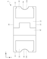
図1~図8は、本発明の実施形態に係る半導体発光装置Aを示す図である。本実施形態に係る半導体発光装置Aは、基材1、半導体発光素子2、配線パターン3、レジスト層4、ワイヤ5、および、封止樹脂6を備えている。
1 to 8 are views showing a semiconductor light emitting device A according to an embodiment of the present invention. The semiconductor light emitting device A according to the present embodiment includes a
図1は、半導体発光装置Aの正面図である。図2は、図1に示した半導体発光装置Aの右側面図(x方向前方側側面)である。図3は、半導体発光装置Aの左側面図(x方向後方側側面)である。図4は、図1に示した半導体発光装置Aの平面図である。図5は、図1に示した半導体発光装置Aの底面図である。図6は、図4から封止樹脂6を透過させて図示した平面図である。なお、図6において、レジスト層4にハッチングし、かつ、透過させている。図7は、図4のVII-VII線に沿う断面図である。図8は、図4のVIII-VIII線に沿う断面図である。
FIG. 1 is a front view of the semiconductor light emitting device A. FIG. 2 is a right side view (front side surface in the x direction) of the semiconductor light emitting device A shown in FIG. FIG. 3 is a left side view (rear side side surface in the x direction) of the semiconductor light emitting device A. FIG. 4 is a plan view of the semiconductor light emitting device A shown in FIG. FIG. 5 is a bottom view of the semiconductor light emitting device A shown in FIG. FIG. 6 is a plan view showing the sealing
図1~図8において、半導体発光装置Aの厚さ方向をz方向、z方向に直角な方向をx方向、x方向およびz方向に直角な方向をy方向とする。また、各方向において、矢印が向く方向を前方とし、その反対方向を後方としている。z方向が本発明の「第1方向」に相当し、x方向が本発明の「第2方向」、y方向が本発明の「第3方向」に相当する。 In FIGS. 1 to 8, the thickness direction of the semiconductor light emitting device A is the z direction, the direction perpendicular to the z direction is the x direction, and the directions perpendicular to the x direction and the z direction are the y direction. Further, in each direction, the direction in which the arrow points is the front, and the opposite direction is the rear. The z direction corresponds to the "first direction" of the present invention, the x direction corresponds to the "second direction" of the present invention, and the y direction corresponds to the "third direction" of the present invention.
基材1は、絶縁性の材料よりなる。このような絶縁性の材料としては、例えば、絶縁性の樹脂もしくはセラミックなどが挙げられる。絶縁性の樹脂としては、例えば、ガラスエポキシ樹脂などが挙げられる。セラミックとしては、例えば、Al2O3、SiC,またはAlNなどが挙げられる。なお、基材1は、アルミニウムなどの金属よりなる基板に、絶縁膜が形成されたものであってもよい。基材1は、z方向視において、x方向に長く伸びた矩形状を呈する。本実施形態においては、基材1は、z方向寸法が、400μmである。基材1は、基材主面11、基材裏面12、一対の第1基材側面13,14、および、一対の第2基材側面15,16を有する。
The
基材主面11および基材裏面12は、図1、図7および図8に示すように、z方向において、離間しており、互いに反対側を向く。基材主面11は、z方向前方を向く面である。基材裏面12は、z方向後方を向く面である。基材主面11および基材裏面12はともに、平坦である。
As shown in FIGS. 1, 7, and 8, the main surface of the
一対の第1基材側面13,14は、図1、図4、図5および図6に示すように、x方向に離間して形成された面である。一対の第1基材側面13,14は、x方向において、互いに反対側を向く。第1基材側面13は、x方向前方側に位置する面であり、第1基材側面14は、x方向後方側に位置する面である。第1基材側面13,14はともに、z方向前方の端部が基材主面11に繋がり、z方向後方の端部が基材裏面12に繋がっている。また、第1基材側面13,14はともに、平坦である。第1基材側面13,14はそれぞれ、スルーホール部131,141を有する。
As shown in FIGS. 1, 4, 5, and 6, the pair of first substrate side surfaces 13 and 14 are surfaces formed apart from each other in the x direction. The pair of first substrate side surfaces 13, 14 face each other in the x direction. The first base
スルーホール部131,141はそれぞれ、第1基材側面13,14から基材1の内側に向け凹んでいる。スルーホール部131,141はともに、基材主面11から基材裏面12に向けて貫通している。本実施形態においては、スルーホール部131,141は、z方向視において、半円形状をなす。
The through-
一対の第2基材側面15,16は、図2~図6および図8に示すように、y方向に離間して形成された面である。一対の第2基材側面15,16は、y方向において、互いに反対側を向く。第2基材側面15は、y方向前方側に位置する面であり、第2基材側面16は、y方向後方側に位置する面である。第2基材側面15,16はともに、z方向前方の端部が基材主面11に繋がり、z方向後方の端部が基材裏面12に繋がっている。また、第2基材側面15,16はともに、平坦である。
As shown in FIGS. 2 to 6 and 8, the pair of second base material side surfaces 15 and 16 are surfaces formed so as to be separated from each other in the y direction. The pair of second substrate side surfaces 15, 16 face each other in the y direction. The second base
半導体発光素子2は、いわゆるLEDチップであり、半導体発光装置Aの光源となる電子部品である。なお、半導体発光素子2は、LEDチップに限定されず、受光素子あるいはダイオードなどであってもよい。半導体発光素子2は、n型半導体層と活性層とp型半導体層とを有する。n型半導体層は活性層に積層されている。活性層はp型半導体層に積層されている。よって、活性層はn型半導体層とp型半導体層との間に位置する。n型半導体層、活性層、および、p型半導体層は、例えば、GaNよりなる。半導体発光素子2は、z方向前方を向く面に第1パッド部を有し、z方向後方を向く面に第2パッド部を有する。なお、これらの図示は省略する。半導体発光素子2は、基材1に搭載されている。半導体発光素子2の発光色は特に限定されない。
The semiconductor
配線パターン3は、半導体発光素子2に電力を供給するための電流経路を構成するものである。配線パターン3は、半導体発光素子2に導通している。配線パターン3は、例えば、Cu、Ni、Ti、Auなどの単種類または複数種類の金属からなる。配線パターン3は基材1に形成されている。本実施形態においては、配線パターン3は、厚さ18μmのCu箔上に厚さ15μmのCuめっきを有している。したがって、配線パターン3は、z方向寸法が33μmである。なお、配線パターン3の構成および厚さ方向寸法はこれに限定されない。配線パターン3は、主面電極31、複数の裏面電極32,33、および、複数の側面電極34,35を有する。
The
主面電極31は、基材1の基材主面11の一部を覆う。主面電極31は、ダイボンディング部311、ワイヤボンディング部312、第1端縁部313、第2端縁部314、第1連結部315、第2連結部316、第1帯状部317、および、第2帯状部318を有している。
The
ダイボンディング部311は、半導体発光素子2を支持する部分である。ダイボンディング部311は、導通性を有する接合材(図示略)により、ダイボンディング部311と第2パッド部とが向かい合うように、半導体発光素子2が接合されている。このような接合材としては、例えば、半田やAgペーストなどが挙げられる。本実施形態においては、ダイボンディング部311は、z方向視において、円形状をなす。なお、ダイボンディング部311は円形状に限らず、矩形状や多角形状などであってもよい。
The
ワイヤボンディング部312は、ワイヤ5をボンディングする部分である。本実施形態においては、ワイヤボンディング部312は、z方向視において、略矩形状をなす。なお、ワイヤボンディング部312の形状は、これに限定されない。
The
第1端縁部313は、基材主面11のうち、スルーホール部131と繋がる部分近傍を覆っている。第2端縁部314は、基材主面11のうち、スルーホール部141と繋がる部分近傍を覆っている。本実施形態においては、第1端縁部313および第2端縁部314はともに、z方向視において、半円環状をなす。また、本実施形態においては、第1端縁部313および第2端縁部314は、図4に示すように、その一部が、レジスト層4および封止樹脂6のいずれからも露出しているため、耐食性を考慮して、Auめっきされている。
The
第1連結部315は、ダイボンディング部311と第1端縁部313とを繋ぐ。第2連結部316は、ワイヤボンディング部312と第2端縁部314とを繋ぐ。本実施形態においては、第1連結部315および第2連結部316はともに、x方向に伸びる帯状をなす。なお、第1連結部315および第2連結部316の形状は、これに限定されない。
The first connecting
第1帯状部317および第2帯状部318は、基材主面11のy方向前方の端部からy方向後方の端部まで繋がっている。第1帯状部317は、基材主面11のx方向前方寄りに配置されている。第2帯状部318は、基材主面11のx方向後方寄りに配置されている。本実施形態においては、第1帯状部317は、第1端縁部313および第1連結部315と繋がっている。また、第2帯状部318は、第2端縁部314および第2連結部316と繋がっている。
The first strip-shaped
裏面電極32,33は、基材裏面12の一部を覆っている。裏面電極32,33は、半導体発光装置Aを実装基板などに実装する際の接合箇所として用いられる。裏面電極32,33は、互いに、x方向に離間し、絶縁されている。裏面電極32はx方向前方寄り配置されており、裏面電極33は、x方向後方寄りに配置されている。
The
側面電極34,35はそれぞれ、基材1のスルーホール部131,141の表面を覆っている。側面電極34,35は、基材主面11から基材裏面12に達している。側面電極34は、z方向前方の端縁が第1端縁部313に繋がり、z方向後方の端縁が裏面電極32に繋がっている。したがって、半導体発光素子2の第2パッド部は、ダイボンディング部311、第1連結部315、第1端縁部313、および、側面電極34を介して、裏面電極32と電気的に接続されている。側面電極35は、z方向前方の端縁が第2端縁部314に繋がり、z方向後方の端縁が裏面電極33に繋がっている。
The
レジスト層4は、基材1に形成され、絶縁性を有する材質からなる。なお、理解の便宜上、一部の図において、レジスト層4にハッチングして示している。レジスト層4は、基材主面側レジスト41と基材裏面側レジスト42とを含んでいる。
The resist
基材主面側レジスト41は、基材1の基材主面11に形成されている。基材主面側レジスト41は、フィルム状のレジストを圧着して貼り付け、硬化させることで、基材主面11に形成される。フィルム状のレジストを圧着するときの圧力により、基材主面側レジスト41には、z方向前方の面が平面となる。基材主面側レジスト41は、パターン被覆部411および基材被覆部413を有する。
The base material main surface side resist 41 is formed on the base material
パターン被覆部411は、基材主面側レジスト41のうち、配線パターン3上に形成された部分である。パターン被覆部411は、z方向前方の面が平坦である。本実施形態においては、パターン被覆部411は、第1帯状部317および第2帯状部318のすべてを覆っている。本実施形態においては、パターン被覆部411は、z方向寸法が、15μmである。パターン被覆部411は、樹脂流出防止部412を有する。
The
樹脂流出防止部412は、後述する封止樹脂6の金型成形工程を用いられる金型71に当接する領域である。樹脂流出防止部412は、z方向視において、封止樹脂6よりx方向外側に位置する。また、樹脂流出防止部412は、z方向視において、第1基材側面13から第1基材側面14までy方向に繋がっている。本実施形態においては、樹脂流出防止部412は、z方向視において、矩形状としている。樹脂流出防止部412のz方向前方の面は、レジスト層4のうち最もz方向前方に位置し、かつ、平坦である。なお、理解の便宜上、一部の図において、樹脂流出防止部412を太い点線で示している。
The resin
基材被覆部413は、基材主面側レジスト41のうち、基材1上に形成された部分である。本実施形態においては、基材被覆部413のz方向寸法は、配線パターン3のz方向寸法とパターン被覆部411のz方向寸法との和より小さい。例えば、基材被覆部413のz方向寸法は40μmである。
The base
基材裏面側レジスト42は、基材1の基材裏面12に形成されている。基材裏面側レジスト42は、基材裏面12のx方向中央付近に形成され、基材裏面12のy方向の両端縁に繋がっている。また、基材裏面側レジスト42は、z方向後方の面が平坦である。本実施形態においては、基材裏面側レジスト42は、z方向寸法が20μmである。また、本実施形態においては、基材裏面側レジスト42は、z方向視において、x方向前方の端縁がx方向前方に突き出た凸字形の形状をなす。このような形状にすることで、半導体発光装置Aの接続方向を判断する目印として機能する。基材裏面側レジスト42は、液体レジストを塗布し、熱硬化させることで、基材裏面12に形成される。なお、基材主面側レジスト41と同様に、フィルム状のレジストを用いて形成してもよい。当該基材裏面側レジスト42が、特許請求の範囲に記載の「絶縁体」に相当する。
The base material back surface side resist 42 is formed on the base material back surface 12 of the
ワイヤ5は、半導体発光素子2と配線パターン3とを導通させるためのものである。ワイヤ5は、例えば、Auなどの金属からなり、ワイヤボンディングによりボンディングされている。ワイヤ5は、一端が半導体発光素子2の第1パッド部にボンディングされ、他端がワイヤボンディング部312にボンディングされている。したがって、半導体発光素子2の第1パッド部は、ワイヤ5、ワイヤボンディング部312、第2連結部316、第2端縁部314、および、側面電極35を介して、裏面電極33と電気的に接続されている。
The
封止樹脂6は、半導体発光素子2、配線パターン3の一部、レジスト層4の一部、および、ワイヤ5を覆っている。封止樹脂6は、光を透過させる樹脂材料からなる。このような樹脂材料として、透明あるいは半透明の、エポキシ樹脂、シリコーン樹脂、アクリル樹脂、もしくは、ポリビニル系樹脂などが挙げられる。また、半導体発光素子2からの光によって励起されることにより異なる波長の光を発する蛍光材料を含むものであってもよい。
The sealing
封止樹脂6は、後述する金型成形工程においてモールド成形により形成される。封止樹脂6は、x方向において、基材1よりも小である。また、封止樹脂6は、z方向前方にドーム形状部61を有する。
The sealing
ドーム形状部61は、封止樹脂6のうち、z方向前方に突出し、半球体形状をなす部分である。当該ドーム形状部61により、半導体発光素子2から発せられた光を所定の方向に照射することができる。すなわち、ドーム形状部61により、封止樹脂6は凸面レンズとして機能する。なお、封止樹脂6の形状は特に限定されない。例えば、半導体発光素子2から発する光を拡散させる場合には、z方向前方の面を凹面にしてもよい。
The dome-shaped
次に、本実施形態に係る半導体発光装置Aの製造方法について、図9~図15を参照し、説明する。本実施形態においては、複数の半導体発光装置Aを製造する場合を例に説明する。本発明に係る半導体発光装置Aの製造方法は、基材準備工程、パターン形成工程、レジスト形成工程、ダイボンディング工程、ワイヤボンディング工程、および、金型成形工程を有する。 Next, a method for manufacturing the semiconductor light emitting device A according to the present embodiment will be described with reference to FIGS. 9 to 15. In this embodiment, a case where a plurality of semiconductor light emitting devices A are manufactured will be described as an example. The method for manufacturing the semiconductor light emitting device A according to the present invention includes a base material preparation step, a pattern forming step, a resist forming step, a die bonding step, a wire bonding step, and a mold forming step.
基材準備工程では、複数の貫通孔101がマトリクス状に形成された、矩形状の集合基材100a(図9参照)を用意する。当該集合基材100aは、図1~図8に示す基材1を複数個形成可能なサイズとされる。図9においては、6個の基材1を形成可能なサイズとし、集合基材100aには、半円形状の貫通孔101が6つ、および、円形状の貫通孔101が3つ形成されている。複数の貫通孔101は、例えば、パンチング処理により形成される。集合基材100aは、上記基材1の材質と同じ、ガラスエポキシ樹脂からなる。
In the base material preparation step, a rectangular
パターン形成工程では、上記集合基材100aに配線パターン3を形成する。配線パターン3は、Cu箔にCuめっきを施すことにより、形成される。当該パターン形成工程により、集合基材100aに配線パターン3が形成された集合基材100b(図10参照)が形成される。
In the pattern forming step, the
レジスト形成工程では、上記配線パターン3を形成した集合基材100bにレジスト層4を形成する。本実施形態においては、集合基材100bのz方向前方の面にフィルム状のレジストを圧着し貼り付ける。そして、露光などにより、硬化させることで、基材主面側レジスト41が形成される。また、集合基材100bのz方向後方の面に液体状のレジストを塗布し、その後、硬化させることで、基材裏面側レジスト42が形成される。当該レジスト形成工程において、基材主面側レジスト41は、フィルム状のレジストを圧着させたときの圧力により、z方向前方側の面は平坦になる。また、形成された基材主面側レジスト41には、配線パターン3上に形成されたパターン被覆部411、および、集合基材100b上(配線パターン3が形成されていない部分)に形成された基材被覆部413が形成されている。本実施形態においては、後述する金型成形工程において、金型71で押さえる領域(図11の点線で囲われた領域)において、パターン被覆部411の一部が、集合基材100cのy方向前方の端縁からy方向後方の端縁まで繋がるように、レジスト層4の貼り付け位置を考慮する。当該レジスト形成工程により、集合基材100bにレジスト層4が形成された集合基材100c(図11参照)が形成される。なお、レジスト形成工程後に、レジスト層4から露出し、かつ、封止樹脂6からも露出させる予定の部分には、Auめっきを施す。
In the resist forming step, the resist
ダイボンディング工程では、半導体発光素子2を、集合基材100cの片面(z方向前方の面)に、周知のダイボンディングの手法によって、搭載する。そして、ワイヤボンディング工程では、ワイヤ5を、周知のワイヤボンディングの手法により、半導体発光素子2の第1パッド部とワイヤボンディング部312とにワイヤボンディングする。これにより、半導体発光素子2と配線パターン3との導通が確保される。これらダイボンディング工程およびワイヤボンディング工程により、集合基材100cに半導体発光素子2およびワイヤ5がボンディングされた集合基材100d(図12参照)が形成される。
In the die bonding step, the semiconductor
金型成形工程では、上記集合基材100dに封止樹脂6をモールド形成する。図13および図14は、金型成形工程を説明するための図である。図13は、金型成形工程における、図12のXIII-XIII線に沿う断面図を示しており、図14は、図13の一点鎖線で示した部分の部分拡大図である。金型成形工程においては、図13に示すように、一対の金型71,72を集合基材100dのz方向から挟み込む。金型71には複数の凹部711が形成されている。当該凹部711の寸法および形状は、封止樹脂6と略同一である。また、金型71は、当接面712を有する。当接面712は、z方向後方を向き、かつ、最もz方向後方側に位置する面である。当接面712は、平坦である。金型71は、当該当接面712により、集合基材100dのz方向前方側の面を押さえている。図12において、当接面712で押さえる領域を細い点線で囲っている。金型72は、z方向前方側の面が一様に平坦であり、集合基材100dのz方向後方側の面を押さえている。
In the mold forming step, the sealing
金型成形工程において、金型71の凹部711内に半導体発光素子2を収容するように、一対の金型71,72で集合基材100dを挟み込む。これにより、凹部711と集合基材100dのうち凹部711に対向する部分とにより、空隙(キャビティ)73が形成される。また、図14に示すように、樹脂流出防止部412が、金型71のz方向後方の面(当接面)712に当接し、かつ、図12に示すように、樹脂流出防止部412が集合基材100dのy方向の一方の端縁から他方の端縁まで連続的に当接している。そして、金型71で集合基材100dを挟み込んだ状態で、金型71に形成された樹脂注入路74から透光性の樹脂材料をキャビティ73内に充填する。そして、これを硬化させることで、封止樹脂6が形成される。なお、樹脂注入路74の位置は限定されない。当該金型成形工程により、集合基材100dに封止樹脂6が形成された集合基材100e(図15参照)が形成される。
In the mold forming step, the
金型成形工程によって、封止樹脂6を形成した後は、図15に示す複数の切断線CLに沿って、集合基材100eを切断する。この切断により、図1~図8に示す半導体発光装置Aを複数個製造することができる。なお、上記半導体発光装置Aの製造方法において、複数の半導体発光装置Aを製造する場合を例に説明したが、1つずつ製造してもよい。
After the sealing
次に、上記実施形態に係る半導体発光装置Aおよび当該半導体発光装置Aの製造方法における作用について説明する。 Next, the operation of the semiconductor light emitting device A according to the above embodiment and the method of manufacturing the semiconductor light emitting device A will be described.
本実施形態によれば、樹脂流出防止部412が、z方向視において、封止樹脂6よりx方向外側に位置し、かつ、z方向視において、第2基材側面15から第2基材側面16までy方向に繋がっている。これにより、封止樹脂6をモールド成形するときに、当該樹脂流出防止部412が金型71(当接面712)に当接するため、レジスト層4(樹脂流出防止部412)と金型71とが密接し、隙間が存在しない。したがって、金型成形工程において、キャビティ73内に樹脂材料を注入したときに、樹脂流出防止部412が障壁となり、上記隙間を介した樹脂漏れを抑制することができる。そして、樹脂漏れが抑制されることで、外部回路との導通経路の確保が可能となり、また、樹脂バリを抑制することができる。
According to the present embodiment, the resin
本実施形態によれば、封止樹脂6のx方向両端縁が全てレジスト層4と当接している。封止樹脂6は、配線パターン3よりレジスト層4との接合性が高い。したがって、封止樹脂6の前記x方向両端縁の接合性を高くすることができ、封止樹脂6のはがれを低減させることができる。
According to this embodiment, all the edges of the sealing
本実施形態によれば、金型成形工程において、樹脂流出防止部412と金型71(当接面712)とを、z方向視において、第2基材側面15から第2基材側面16までy方向に繋がって当接させることで、樹脂漏れを抑制している。従来の半導体発光装置の金型成形工程において、一対の金型で挟み込むときの型締力を高くすることで、上記隙間を防ぎ、樹脂漏れを抑制することも可能であるが、当該型締力を高くすると、その型締力に基材が耐えられず、基材割れなどの要因となってしまう。特に、薄型の半導体発光装置の場合、当該課題は顕著に表れる。したがって、半導体発光装置Aは、金型成形工程において、一対の金型71,72の型締力を、従来のように高くすることなく、樹脂漏れを抑制することが可能となる。これにより、基材割れなどを低減することができる。さらに、高い型締力でプレス可能な金型成形機が不要となり、製造コストの抑制にも寄与することができる。
According to the present embodiment, in the mold forming step, the resin
本実施形態によれば、レジスト形成工程において、基材主面側レジスト41としてフィルム状のレジストを用いた。フィルム状のレジストは液体状のレジストと比べ、パターニング精度がよい。このパターニング精度により、スルーホール部131,141が形成されている場合、液体状のレジストにおいては、スルーホール部131,141から0.125mm以上離れた位置でなければ塗布できなかった。一方、フィルム状のレジストにおいては、スルーホール部131,141からの距離を0.05mm程度まで近づけることができるため、樹脂流出防止部412の形成が容易になる。また、フィルム状のレジストを圧着により貼り付けるため、液体状のレジストを塗布する場合に比べて、平面を形成しやすい。したがって、樹脂流出防止部412のz方向前方の面が平坦にしやすいため、金型71との密着性を高めることができる。なお、液体状のレジストであっても、フィルム状のレジストと同等のパターニングが可能であれば、液体のソルダーレジストにより基材主面側レジスト41を形成してもよい。
According to this embodiment, in the resist forming step, a film-like resist was used as the resist 41 on the main surface side of the substrate. The film-like resist has better patterning accuracy than the liquid-like resist. Due to this patterning accuracy, when the through-
本実施形態によれば、金型成形工程において、樹脂流出防止部412(レジスト層4)が、金型71(当接面712)に当接しており、配線パターン3に当接しない。したがって、配線パターン3に上記型締力が加わらないため、配線パターン3の断線を抑制することができる。
According to the present embodiment, in the mold forming step, the resin outflow prevention portion 412 (resist layer 4) is in contact with the mold 71 (contact surface 712) and does not abut on the
上記実施形態において、配線パターン3およびレジスト層4の配置位置は上記したものに限定されず、金型成形工程において、当接面712に当接する樹脂流出防止部412が、第2基材側面15から第2基材側面16までy方向に繋がっていればどのような配置であってもよい。このような、配線パターン3およびレジスト層4の片方あるいは両方が、上記半導体発光装置Aと異なる変形例について、説明する。なお、上記半導体発光装置Aと同一あるいは類似の構成については、同一の符号を付して、その説明を省略する。
In the above embodiment, the arrangement positions of the
図16は、第1変形例に係る各種半導体発光装置A1を示している。図16は、上記図6に対応する平面図であり、封止樹脂6の記載を省略し、金型71の当接面712を点線で示している。換言すれば、金型成形工程において、樹脂材料(封止樹脂6)をキャビティ73内に充填する前の状態を示している。なお、図16においては、x方向前方部分のみを図示している。
FIG. 16 shows various semiconductor light emitting devices A1 according to the first modification. FIG. 16 is a plan view corresponding to FIG. 6, omitting the description of the sealing
図16(a)は、パターン被覆部411が、第1帯状部317のすべてを覆っていない場合の変形例を示している。図16(b)は、図示している基材主面側レジスト41のx方向後方の端縁が、曲線である場合の変形例を示している。図16(c)は、配線パターン3(第1帯状部317)の形状が異なる場合の変形例を示している。
FIG. 16A shows a modified example in which the
図16(a)~(c)においても、太い点線で示した樹脂流出防止部412が、z方向視において、第2基材側面15から第2基材側面16までy方向に繋がっている。したがって、これらのような第1変形例においても上記実施形態と同様に、金型成形工程において、樹脂流出防止部412が障壁となり、上記隙間を介した樹脂漏れを抑制することができる。また、金型成形工程より封止樹脂6が形成された半導体発光装置A1において、樹脂流出防止部412が封止樹脂6よりx方向外側に位置する。
Also in FIGS. 16A to 16C, the resin
図17は、第2変形例に係る各種半導体発光装置A2を示している。図17は、図16に対応する平面図である。上記実施形態に係る半導体発光装置Aおよび第1変形例に係る半導体発光装置A1は、樹脂流出防止部412がz方向視において平面状であったが、第2変形例に係る半導体発光装置A2は、樹脂流出防止部412がz方向視において線状になっている。
FIG. 17 shows various semiconductor light emitting devices A2 according to the second modification. FIG. 17 is a plan view corresponding to FIG. In the semiconductor light emitting device A according to the above embodiment and the semiconductor light emitting device A1 according to the first modification, the resin
図17(a)は、第1帯状部317のx方向前方の端縁と基材主面側レジスト41(パターン被覆部411)のx方向後方の端縁とがz方向視において一致している場合を示している。図17(b)は、第1帯状部317のx方向前方の端縁と、基材主面側レジスト41(パターン被覆部411)のx方向前方の端縁と、金型71の当接面712のx方向後方の端縁とがz方向視において一致している場合を示している。
In FIG. 17A, the front edge of the first band-shaped
図17(a),(b)において、樹脂流出防止部412が、線状に、z方向視において、第2基材側面15から第2基材側面16までy方向に繋がっている。したがって、これらのような第2変形例においても上記実施形態と同様に、金型成形工程において、樹脂流出防止部412が障壁となり、上記隙間を介した樹脂漏れを抑制することができる。なお、図17(a),(b)で示す半導体発光装置A2において、金型成形工程より封止樹脂6が形成されたとき、封止樹脂6の外側の端縁と樹脂流出防止部412とは、z方向視において一致している。
In FIGS. 17A and 17B, the resin
上記半導体発光装置A,A1,A2においては、基材被覆部413のz方向寸法が、配線パターン3のz方向寸法とパターン被覆部411のz方向寸法との和より小さい場合を例に説明したが、これに限定されない。例えば、基材被覆部413のz方向寸法が、配線パターン3のz方向寸法とパターン被覆部411のz方向寸法との和と同じであってもよい。すなわち、基材被覆部413のz方向寸法を、48μm(33μm(配線パターン3のz方向寸法)+15μm(パターン被覆部411のz方向寸法))としてもよい。この場合、金型成形工程における樹脂材料の注入時に、樹脂流出防止部412だけでなく、基材被覆部413も障壁となるため、樹脂漏れをさらに抑制することができる。また、樹脂流出防止部412が、z方向視において、第2基材側面15から第2基材側面16までy方向に繋がっていなくても、基材被覆部413と樹脂流出防止部412とで、z方向視において、第2基材側面15から第2基材側面16までy方向に繋がっていれば、同様に、樹脂漏れを抑制することができる。
In the semiconductor light emitting devices A, A1, and A2, the case where the z-direction dimension of the base
本発明に係る半導体発光装置および当該半導体発光装置の製造方法は、上記した実施形態に限定されるものではない。本発明の半導体発光装置の各部の具体的な構成および当該半導体発光装置の製造方法の各工程の具体的な手順や方法は、種々に設計変更自在である。 The semiconductor light emitting device according to the present invention and the method for manufacturing the semiconductor light emitting device are not limited to the above-described embodiment. The specific configuration of each part of the semiconductor light emitting device of the present invention and the specific procedure and method of each step of the manufacturing method of the semiconductor light emitting device can be variously redesigned.
A,A1,A2:半導体発光装置
1 :基材
11 :基材主面
12 :基材裏面
13,14 :第1基材側面
131,141:スルーホール部
15,16 :第2基材側面
2 :半導体素子
3 :配線パターン
31 :主面電極
311 :ダイボンディング部
312 :ワイヤボンディング部
313 :第1端縁部
314 :第2端縁部
315 :第1連結部
316 :第2連結部
317 :第1帯状部
318 :第2帯状部
32,33 :裏面電極
34,35 :側面電極
4 :レジスト層
41 :基材主面側レジスト
411 :パターン被覆部
412 :樹脂流出防止部
413 :基材被覆部
42 :基材裏面側レジスト
5 :ワイヤ
6 :封止樹脂
61 :ドーム形状部
100a,100b,100c,100d,100e:集合基材
101 :貫通孔
71,72 :金型
711 :凹部
712 :当接面
73 :キャビティ
74 :樹脂注入路
A, A1, A2: Semiconductor light emitting device 1: Base material 11: Base material main surface 12: Base material back
Claims (24)
前記基材主面に搭載された半導体発光素子と、
前記半導体発光素子を覆い、かつ、透光性を有し、前記第1方向視において、前記基材より小である封止樹脂と、
前記基材主面に形成された主面電極を有し、前記半導体発光素子への導通経路である配線パターンと、
前記第1方向視において、前記主面電極と重なるパターン被覆部を有し、絶縁性の材質からなるレジスト層と、
を備えており、
前記封止樹脂は、前記第2方向の端縁が一方の前記第2基材側面から他方の前記第2基材側面まで前記第3方向に繋がり、
前記パターン被覆部は、前記封止樹脂の前記第2方向の前記端縁の全長に対して前記第2方向における外側に接し、かつ、前記第1方向視において、一方の前記第2基材側面から他方の前記第2基材側面まで前記第3方向に繋がるとともに前記第1方向前方の面が平坦である樹脂流出防止部を有しており、
前記主面電極は、互いに離間する第1部分および第2部分を有し、
前記レジスト層は、前記第1方向視において前記第1部分に重なる第1レジスト層、および、前記第1レジスト層から離間し、かつ、前記第1方向視において前記第2部分に重なる第2レジスト層を有し、
前記第1レジスト層および前記第2レジスト層は、前記樹脂流出防止部を含む前記パターン被覆部に対して前記第2方向の内方に繋がり且つ前記基材主面と前記封止樹脂とに接して挟まれた内方基材被覆部と、前記パターン被覆部に対して前記第2方向の外方に繋がり且つ前記基材主面に接する外方基材被覆部と、を有し、
前記パターン被覆部、前記内方基材被覆部および前記外方基材被覆部は、前記第2方向視において互いに重なる部分を有し、
前記第1レジスト層の前記外方基材被覆部は、前記第1方向視において一方の前記第1基材側面に重なり、
前記第2レジスト層の前記外方基材被覆部は、前記第1方向視において他方の前記第1基材側面から離間している、ことを特徴とする半導体発光装置。 A pair of first units having a main surface of a base material facing forward in the first direction and a back surface of a base material facing backward in the first direction in the first direction and facing opposite sides in the second direction perpendicular to the first direction. A substrate having a side surface of the material, a pair of second substrate sides facing each other in a third direction perpendicular to the first direction and the second direction, and a substrate.
The semiconductor light emitting device mounted on the main surface of the base material and
A sealing resin that covers the semiconductor light emitting device, has translucency, and is smaller than the base material in the first direction view.
A wiring pattern having a main surface electrode formed on the main surface of the base material and being a conduction path to the semiconductor light emitting device,
In the first direction view, a resist layer having a pattern covering portion overlapping with the main surface electrode and made of an insulating material,
Equipped with
In the sealing resin, the edge in the second direction is connected in the third direction from one side surface of the second base material to the other side surface of the second base material.
The pattern covering portion is in contact with the outer side in the second direction with respect to the total length of the edge of the sealing resin in the second direction, and is one side surface of the second base material in the first direction view. It has a resin outflow prevention portion which is connected to the other side surface of the second base material in the third direction and whose front surface in the first direction is flat.
The main surface electrode has a first portion and a second portion that are separated from each other.
The resist layer is a first resist layer that overlaps the first portion in the first direction view, and a second resist that is separated from the first resist layer and overlaps the second portion in the first direction view. Has layers and
The first resist layer and the second resist layer are connected inward in the second direction to the pattern covering portion including the resin outflow prevention portion, and are in contact with the main surface of the base material and the sealing resin. It has an inner base material covering portion sandwiched between the two, and an outer base material covering portion that is connected to the outer side of the pattern covering portion in the second direction and is in contact with the main surface of the base material.
The pattern coating portion, the inner substrate coating portion, and the outer substrate coating portion have portions that overlap each other in the second direction view.
The outer substrate coating portion of the first resist layer overlaps with one side surface of the first substrate in the first direction view.
A semiconductor light emitting device , wherein the outer substrate coating portion of the second resist layer is separated from the other side surface of the first substrate in the first direction view .
前記第2レジスト層の前記一対の端縁の各々は、前記第1方向視において、前記第3方向に沿った直線部と他方の端縁に向けて凹んだ形状の湾曲部とを有している、
請求項1に記載の半導体発光装置。 The second resist layer has a pair of edge edges that are separated from each other in the second direction.
Each of the pair of edges of the second resist layer has, in the first direction, a straight portion along the third direction and a curved portion having a shape recessed toward the other edge. Yes,
The semiconductor light emitting device according to claim 1 .
請求項2に記載の半導体発光装置。 The pair of first base material side surfaces have a first through-hole portion and a second through-hole portion that are recessed in the second direction and penetrate from the base material main surface to the back surface of the base material, respectively.
The semiconductor light emitting device according to claim 2 .
請求項3に記載の半導体発光装置。 The first through-hole portion and the second through-hole portion form a semicircular shape in the first directional view.
The semiconductor light emitting device according to claim 3 .
請求項3または請求項4に記載の半導体発光装置。 Of the pair of edge edges of the second resist layer, the curved portion of the edge located on the second through-hole portion side in the second direction is curved along the second through-hole portion. ,
The semiconductor light emitting device according to claim 3 or 4 .
請求項3ないし請求項5のいずれか一項に記載の半導体発光装置。 The wiring pattern is formed on the surface of the first through-hole portion and is formed on the surface of the first side surface electrode connected to the first portion and the surface of the second through-hole portion, and the second portion. Has a second side electrode that leads to
The semiconductor light emitting device according to any one of claims 3 to 5 .
請求項6に記載の半導体発光装置。 The wiring pattern is formed on the back surface of the base material and is connected to the first side surface electrode, and the second back surface electrode is formed on the back surface of the base material and is connected to the second side surface electrode. Have,
The semiconductor light emitting device according to claim 6 .
請求項7に記載の半導体発光装置。 The first back surface electrode and the second back surface electrode are isolated from each other and insulated.
The semiconductor light emitting device according to claim 7 .
請求項8に記載の半導体発光装置。 An insulator is arranged between the first back surface electrode and the second back surface electrode.
The semiconductor light emitting device according to claim 8 .
請求項7ないし請求項9のいずれか一項に記載の半導体発光装置。 Further, a wire for connecting the semiconductor light emitting device and the wiring pattern is provided.
The semiconductor light emitting device according to any one of claims 7 to 9 .
前記第2部分は、前記ワイヤを介して前記半導体発光素子と導通するワイヤボンディング部を有する、
請求項10に記載の半導体発光装置。 The first portion has a die bonding portion to which the semiconductor light emitting device is die bonded.
The second portion has a wire bonding portion that conducts with the semiconductor light emitting device via the wire.
The semiconductor light emitting device according to claim 10 .
前記第1パッド部は、前記ワイヤがボンディングされ、前記ワイヤボンディング部と導通し、
前記第2パッド部は、導通性接合材により前記ダイボンディング部に接合され、前記ダイボンディング部と導通している、
請求項11に記載の半導体発光装置。 The semiconductor light emitting device has a first pad portion facing forward in the first direction and a second pad portion facing rearward in the first direction.
In the first pad portion, the wire is bonded and conducts with the wire bonding portion.
The second pad portion is bonded to the die bonding portion by a conductive bonding material and is conductive to the die bonding portion.
The semiconductor light emitting device according to claim 11 .
請求項12に記載の半導体発光装置。 The first portion is arranged in the vicinity of the portion connected to the first through-hole portion in the first directional view, and is connected to the first side surface electrode, the first end edge portion, the first end edge portion, and the die. It has a first connecting portion that connects the bonding portion.
The semiconductor light emitting device according to claim 12 .
請求項13に記載の半導体発光装置。 The first portion is connected to the first connecting portion, and in the first direction view, the first strip-shaped portion extending from one end edge of the third direction of the base material main surface toward the other end edge. , Further
The semiconductor light emitting device according to claim 13 .
請求項14に記載の半導体発光装置。 The resin outflow prevention portion includes a first prevention portion that overlaps the first band-shaped portion in the first direction view.
The semiconductor light emitting device according to claim 14 .
請求項13ないし請求項15のいずれか一項に記載の半導体発光装置。 The second portion is arranged in the vicinity of the portion connected to the second through-hole portion in the first directional view, and is connected to the second side surface electrode, the second end edge portion, the second end edge portion, and the wire. It has a second connecting portion that connects the bonding portion.
The semiconductor light emitting device according to any one of claims 13 to 15 .
請求項16に記載の半導体発光装置。 The second portion is connected to the second connecting portion, and in the first direction view, the second strip-shaped portion extending from one end edge of the third direction of the base material main surface toward the other end edge. , Further
The semiconductor light emitting device according to claim 16 .
請求項17に記載の半導体発光装置。 The resin outflow prevention portion includes a second prevention portion that overlaps the second band-shaped portion in the first direction view.
The semiconductor light emitting device according to claim 17 .
請求項1ないし請求項18のいずれか一項に記載の半導体発光装置。 The wiring pattern is made of Cu.
The semiconductor light emitting device according to any one of claims 1 to 18 .
請求項19に記載の半導体発光装置。 In the wiring pattern, Au plating is applied to a portion exposed from the sealing resin and also exposed from the resist layer.
The semiconductor light emitting device according to claim 19 .
請求項1ないし請求項20のいずれか一項に記載の半導体発光装置。 The sealing resin is made of an epoxy resin, a silicone resin, an acrylic resin, or a polyvinyl resin resin material.
The semiconductor light emitting device according to any one of claims 1 to 20 .
請求項21に記載の半導体発光装置。 The sealing resin has a dome-shaped dome-shaped portion protruding forward in the first direction.
The semiconductor light emitting device according to claim 21 .
請求項1ないし請求項22のいずれか一項に記載の半導体発光装置。 A part of the resist layer is interposed between the sealing resin and the main surface of the base material, and the part is directly attached to each of the sealing resin and the main surface of the base material. In contact,
The semiconductor light emitting device according to any one of claims 1 to 22 .
請求項23に記載の半導体発光装置。 The upper surface of the part of the resist layer is flush with the upper surface of the resin outflow prevention portion.
The semiconductor light emitting device according to claim 23 .
Priority Applications (3)
| Application Number | Priority Date | Filing Date | Title |
|---|---|---|---|
| JP2016138140A JP7029223B2 (en) | 2016-07-13 | 2016-07-13 | Semiconductor light emitting device |
| US15/643,136 US10319887B2 (en) | 2016-07-13 | 2017-07-06 | Semiconductor light-emitting device and method for manufacturing the same |
| CN201710565645.3A CN107623065A (en) | 2016-07-13 | 2017-07-12 | Light emitting semiconductor device and its manufacture method |
Applications Claiming Priority (1)
| Application Number | Priority Date | Filing Date | Title |
|---|---|---|---|
| JP2016138140A JP7029223B2 (en) | 2016-07-13 | 2016-07-13 | Semiconductor light emitting device |
Publications (3)
| Publication Number | Publication Date |
|---|---|
| JP2018010949A JP2018010949A (en) | 2018-01-18 |
| JP2018010949A5 JP2018010949A5 (en) | 2019-04-18 |
| JP7029223B2 true JP7029223B2 (en) | 2022-03-03 |
Family
ID=60940741
Family Applications (1)
| Application Number | Title | Priority Date | Filing Date |
|---|---|---|---|
| JP2016138140A Active JP7029223B2 (en) | 2016-07-13 | 2016-07-13 | Semiconductor light emitting device |
Country Status (3)
| Country | Link |
|---|---|
| US (1) | US10319887B2 (en) |
| JP (1) | JP7029223B2 (en) |
| CN (1) | CN107623065A (en) |
Families Citing this family (5)
| Publication number | Priority date | Publication date | Assignee | Title |
|---|---|---|---|---|
| KR20190098709A (en) * | 2018-02-14 | 2019-08-22 | 에피스타 코포레이션 | Light-emitting device, manufacturing method thereof and display module using the same |
| US11322459B2 (en) * | 2018-03-12 | 2022-05-03 | Rohm Co., Ltd. | Lead of semiconductor device having a side surface with a plurality of recess areas |
| JP2020025034A (en) * | 2018-08-08 | 2020-02-13 | ローム株式会社 | Led package and led display device |
| JP2020027824A (en) * | 2018-08-09 | 2020-02-20 | ローム株式会社 | Light-emitting device and display device |
| TWI819073B (en) * | 2019-08-22 | 2023-10-21 | 晶元光電股份有限公司 | Light-emitting device, manufacturing method thereof and display module using the same |
Citations (9)
| Publication number | Priority date | Publication date | Assignee | Title |
|---|---|---|---|---|
| JP2007088155A (en) | 2005-09-21 | 2007-04-05 | Stanley Electric Co Ltd | Surface-mounted led board |
| JP2007201171A (en) | 2006-01-26 | 2007-08-09 | Sony Corp | Light source device and display device |
| JP2007258324A (en) | 2006-03-22 | 2007-10-04 | Matsushita Electric Ind Co Ltd | Light-emitting device and manufacturing method thereof |
| JP2009130195A (en) | 2007-11-26 | 2009-06-11 | Stanley Electric Co Ltd | Semiconductor light emitting device |
| JP2011023461A (en) | 2009-07-14 | 2011-02-03 | Panasonic Corp | Semiconductor device |
| JP2011077164A (en) | 2009-09-29 | 2011-04-14 | Sanken Electric Co Ltd | Semiconductor light-emitting device |
| JP2012186450A (en) | 2011-02-16 | 2012-09-27 | Rohm Co Ltd | Led module |
| US20130134471A1 (en) | 2011-11-30 | 2013-05-30 | Lite-On Technology Corporation | Led substrate structure, led unit and lighting module having the same |
| JP2015115432A (en) | 2013-12-11 | 2015-06-22 | ローム株式会社 | Semiconductor device |
Family Cites Families (8)
| Publication number | Priority date | Publication date | Assignee | Title |
|---|---|---|---|---|
| JPS6194362U (en) * | 1984-11-26 | 1986-06-18 | ||
| JPH08321634A (en) * | 1995-05-26 | 1996-12-03 | Stanley Electric Co Ltd | Surface mount type light-emitting diode |
| JP3065509B2 (en) * | 1995-06-02 | 2000-07-17 | スタンレー電気株式会社 | Surface mount type light emitting diode |
| JP3158018B2 (en) * | 1995-07-17 | 2001-04-23 | シャープ株式会社 | Horizontal light emitting LED and method for manufacturing the same |
| JPH11298049A (en) * | 1998-04-16 | 1999-10-29 | Matsushita Electron Corp | Light-emission display device |
| EP1928026A1 (en) * | 2006-11-30 | 2008-06-04 | Toshiba Lighting & Technology Corporation | Illumination device with semiconductor light-emitting elements |
| US20110284914A1 (en) * | 2008-11-25 | 2011-11-24 | Denki Kagaku Kogyo Kabushiki Kaisha | Method for manufacturing substrate for light emitting element package, and light emitting element package |
| KR102634692B1 (en) * | 2016-02-12 | 2024-02-08 | 삼성전자주식회사 | Semiconductor light emitting device package |
-
2016
- 2016-07-13 JP JP2016138140A patent/JP7029223B2/en active Active
-
2017
- 2017-07-06 US US15/643,136 patent/US10319887B2/en active Active
- 2017-07-12 CN CN201710565645.3A patent/CN107623065A/en active Pending
Patent Citations (9)
| Publication number | Priority date | Publication date | Assignee | Title |
|---|---|---|---|---|
| JP2007088155A (en) | 2005-09-21 | 2007-04-05 | Stanley Electric Co Ltd | Surface-mounted led board |
| JP2007201171A (en) | 2006-01-26 | 2007-08-09 | Sony Corp | Light source device and display device |
| JP2007258324A (en) | 2006-03-22 | 2007-10-04 | Matsushita Electric Ind Co Ltd | Light-emitting device and manufacturing method thereof |
| JP2009130195A (en) | 2007-11-26 | 2009-06-11 | Stanley Electric Co Ltd | Semiconductor light emitting device |
| JP2011023461A (en) | 2009-07-14 | 2011-02-03 | Panasonic Corp | Semiconductor device |
| JP2011077164A (en) | 2009-09-29 | 2011-04-14 | Sanken Electric Co Ltd | Semiconductor light-emitting device |
| JP2012186450A (en) | 2011-02-16 | 2012-09-27 | Rohm Co Ltd | Led module |
| US20130134471A1 (en) | 2011-11-30 | 2013-05-30 | Lite-On Technology Corporation | Led substrate structure, led unit and lighting module having the same |
| JP2015115432A (en) | 2013-12-11 | 2015-06-22 | ローム株式会社 | Semiconductor device |
Also Published As
| Publication number | Publication date |
|---|---|
| US20180019383A1 (en) | 2018-01-18 |
| CN107623065A (en) | 2018-01-23 |
| US10319887B2 (en) | 2019-06-11 |
| JP2018010949A (en) | 2018-01-18 |
Similar Documents
| Publication | Publication Date | Title |
|---|---|---|
| JP7029223B2 (en) | Semiconductor light emitting device | |
| JP5038623B2 (en) | Optical semiconductor device and manufacturing method thereof | |
| JP5802695B2 (en) | Semiconductor device and method for manufacturing semiconductor device | |
| JP4045781B2 (en) | Light emitting device | |
| JP4122784B2 (en) | Light emitting device | |
| JP6892261B2 (en) | LED package | |
| JP4910220B1 (en) | LED module device and manufacturing method thereof | |
| CN110383464B (en) | Semiconductor device with a semiconductor device having a plurality of semiconductor chips | |
| JP4904604B1 (en) | LED module device and manufacturing method thereof | |
| US9899357B2 (en) | LED module | |
| JP7337590B2 (en) | semiconductor light emitting device | |
| US10847689B2 (en) | Semiconductor light emitting device and method of manufacturing the same | |
| JP2011077164A (en) | Semiconductor light-emitting device | |
| JP6651699B2 (en) | Manufacturing method of side emission type light emitting device | |
| JP6899226B2 (en) | Semiconductor device | |
| US10211179B2 (en) | Semiconductor device | |
| JP6626311B2 (en) | Semiconductor device | |
| JP6543391B2 (en) | Semiconductor device | |
| JP5998716B2 (en) | Light emitting device | |
| JP2017157687A (en) | Led light-emitting device | |
| JP2017157683A (en) | Led light-emitting device and manufacturing method thereof | |
| JP7089343B2 (en) | Semiconductor light emitting device | |
| JP2019110292A (en) | Semiconductor light-emitting device | |
| JP2020074488A (en) | Light-emitting device | |
| JP2014067933A (en) | Light emitting device |
Legal Events
| Date | Code | Title | Description |
|---|---|---|---|
| A521 | Request for written amendment filed |
Free format text: JAPANESE INTERMEDIATE CODE: A523 Effective date: 20190307 |
|
| A621 | Written request for application examination |
Free format text: JAPANESE INTERMEDIATE CODE: A621 Effective date: 20190621 |
|
| A977 | Report on retrieval |
Free format text: JAPANESE INTERMEDIATE CODE: A971007 Effective date: 20200415 |
|
| A131 | Notification of reasons for refusal |
Free format text: JAPANESE INTERMEDIATE CODE: A131 Effective date: 20200707 |
|
| A521 | Request for written amendment filed |
Free format text: JAPANESE INTERMEDIATE CODE: A523 Effective date: 20200901 |
|
| A131 | Notification of reasons for refusal |
Free format text: JAPANESE INTERMEDIATE CODE: A131 Effective date: 20210105 |
|
| A521 | Request for written amendment filed |
Free format text: JAPANESE INTERMEDIATE CODE: A523 Effective date: 20210222 |
|
| A02 | Decision of refusal |
Free format text: JAPANESE INTERMEDIATE CODE: A02 Effective date: 20210817 |
|
| A521 | Request for written amendment filed |
Free format text: JAPANESE INTERMEDIATE CODE: A523 Effective date: 20211108 |
|
| C60 | Trial request (containing other claim documents, opposition documents) |
Free format text: JAPANESE INTERMEDIATE CODE: C60 Effective date: 20211108 |
|
| A911 | Transfer to examiner for re-examination before appeal (zenchi) |
Free format text: JAPANESE INTERMEDIATE CODE: A911 Effective date: 20211115 |
|
| C21 | Notice of transfer of a case for reconsideration by examiners before appeal proceedings |
Free format text: JAPANESE INTERMEDIATE CODE: C21 Effective date: 20211116 |
|
| TRDD | Decision of grant or rejection written | ||
| A01 | Written decision to grant a patent or to grant a registration (utility model) |
Free format text: JAPANESE INTERMEDIATE CODE: A01 Effective date: 20220125 |
|
| A61 | First payment of annual fees (during grant procedure) |
Free format text: JAPANESE INTERMEDIATE CODE: A61 Effective date: 20220218 |
|
| R150 | Certificate of patent or registration of utility model |
Ref document number: 7029223 Country of ref document: JP Free format text: JAPANESE INTERMEDIATE CODE: R150 |