JP7010633B2 - Semiconductor manufacturing equipment and methods for manufacturing semiconductor equipment - Google Patents
Semiconductor manufacturing equipment and methods for manufacturing semiconductor equipment Download PDFInfo
- Publication number
- JP7010633B2 JP7010633B2 JP2017178969A JP2017178969A JP7010633B2 JP 7010633 B2 JP7010633 B2 JP 7010633B2 JP 2017178969 A JP2017178969 A JP 2017178969A JP 2017178969 A JP2017178969 A JP 2017178969A JP 7010633 B2 JP7010633 B2 JP 7010633B2
- Authority
- JP
- Japan
- Prior art keywords
- die
- region
- lighting device
- image pickup
- illuminates
- Prior art date
- Legal status (The legal status is an assumption and is not a legal conclusion. Google has not performed a legal analysis and makes no representation as to the accuracy of the status listed.)
- Active
Links
Images


Classifications
-
- H—ELECTRICITY
- H01—ELECTRIC ELEMENTS
- H01L—SEMICONDUCTOR DEVICES NOT COVERED BY CLASS H10
- H01L21/00—Processes or apparatus adapted for the manufacture or treatment of semiconductor or solid state devices or of parts thereof
- H01L21/67—Apparatus specially adapted for handling semiconductor or electric solid state devices during manufacture or treatment thereof; Apparatus specially adapted for handling wafers during manufacture or treatment of semiconductor or electric solid state devices or components ; Apparatus not specifically provided for elsewhere
- H01L21/67005—Apparatus not specifically provided for elsewhere
- H01L21/67242—Apparatus for monitoring, sorting or marking
-
- H—ELECTRICITY
- H01—ELECTRIC ELEMENTS
- H01L—SEMICONDUCTOR DEVICES NOT COVERED BY CLASS H10
- H01L21/00—Processes or apparatus adapted for the manufacture or treatment of semiconductor or solid state devices or of parts thereof
- H01L21/67—Apparatus specially adapted for handling semiconductor or electric solid state devices during manufacture or treatment thereof; Apparatus specially adapted for handling wafers during manufacture or treatment of semiconductor or electric solid state devices or components ; Apparatus not specifically provided for elsewhere
- H01L21/67005—Apparatus not specifically provided for elsewhere
- H01L21/67011—Apparatus for manufacture or treatment
- H01L21/67144—Apparatus for mounting on conductive members, e.g. leadframes or conductors on insulating substrates
-
- H—ELECTRICITY
- H01—ELECTRIC ELEMENTS
- H01L—SEMICONDUCTOR DEVICES NOT COVERED BY CLASS H10
- H01L21/00—Processes or apparatus adapted for the manufacture or treatment of semiconductor or solid state devices or of parts thereof
- H01L21/02—Manufacture or treatment of semiconductor devices or of parts thereof
- H01L21/04—Manufacture or treatment of semiconductor devices or of parts thereof the devices having at least one potential-jump barrier or surface barrier, e.g. PN junction, depletion layer or carrier concentration layer
- H01L21/50—Assembly of semiconductor devices using processes or apparatus not provided for in a single one of the subgroups H01L21/06 - H01L21/326, e.g. sealing of a cap to a base of a container
- H01L21/52—Mounting semiconductor bodies in containers
-
- H—ELECTRICITY
- H01—ELECTRIC ELEMENTS
- H01L—SEMICONDUCTOR DEVICES NOT COVERED BY CLASS H10
- H01L21/00—Processes or apparatus adapted for the manufacture or treatment of semiconductor or solid state devices or of parts thereof
- H01L21/67—Apparatus specially adapted for handling semiconductor or electric solid state devices during manufacture or treatment thereof; Apparatus specially adapted for handling wafers during manufacture or treatment of semiconductor or electric solid state devices or components ; Apparatus not specifically provided for elsewhere
- H01L21/67005—Apparatus not specifically provided for elsewhere
- H01L21/67011—Apparatus for manufacture or treatment
- H01L21/67092—Apparatus for mechanical treatment
-
- H—ELECTRICITY
- H01—ELECTRIC ELEMENTS
- H01L—SEMICONDUCTOR DEVICES NOT COVERED BY CLASS H10
- H01L21/00—Processes or apparatus adapted for the manufacture or treatment of semiconductor or solid state devices or of parts thereof
- H01L21/67—Apparatus specially adapted for handling semiconductor or electric solid state devices during manufacture or treatment thereof; Apparatus specially adapted for handling wafers during manufacture or treatment of semiconductor or electric solid state devices or components ; Apparatus not specifically provided for elsewhere
- H01L21/67005—Apparatus not specifically provided for elsewhere
- H01L21/67011—Apparatus for manufacture or treatment
- H01L21/67121—Apparatus for making assemblies not otherwise provided for, e.g. package constructions
-
- H—ELECTRICITY
- H01—ELECTRIC ELEMENTS
- H01L—SEMICONDUCTOR DEVICES NOT COVERED BY CLASS H10
- H01L21/00—Processes or apparatus adapted for the manufacture or treatment of semiconductor or solid state devices or of parts thereof
- H01L21/67—Apparatus specially adapted for handling semiconductor or electric solid state devices during manufacture or treatment thereof; Apparatus specially adapted for handling wafers during manufacture or treatment of semiconductor or electric solid state devices or components ; Apparatus not specifically provided for elsewhere
- H01L21/67005—Apparatus not specifically provided for elsewhere
- H01L21/67011—Apparatus for manufacture or treatment
- H01L21/67132—Apparatus for placing on an insulating substrate, e.g. tape
-
- H—ELECTRICITY
- H01—ELECTRIC ELEMENTS
- H01L—SEMICONDUCTOR DEVICES NOT COVERED BY CLASS H10
- H01L21/00—Processes or apparatus adapted for the manufacture or treatment of semiconductor or solid state devices or of parts thereof
- H01L21/67—Apparatus specially adapted for handling semiconductor or electric solid state devices during manufacture or treatment thereof; Apparatus specially adapted for handling wafers during manufacture or treatment of semiconductor or electric solid state devices or components ; Apparatus not specifically provided for elsewhere
- H01L21/67005—Apparatus not specifically provided for elsewhere
- H01L21/67242—Apparatus for monitoring, sorting or marking
- H01L21/67288—Monitoring of warpage, curvature, damage, defects or the like
-
- H—ELECTRICITY
- H01—ELECTRIC ELEMENTS
- H01L—SEMICONDUCTOR DEVICES NOT COVERED BY CLASS H10
- H01L22/00—Testing or measuring during manufacture or treatment; Reliability measurements, i.e. testing of parts without further processing to modify the parts as such; Structural arrangements therefor
- H01L22/10—Measuring as part of the manufacturing process
- H01L22/12—Measuring as part of the manufacturing process for structural parameters, e.g. thickness, line width, refractive index, temperature, warp, bond strength, defects, optical inspection, electrical measurement of structural dimensions, metallurgic measurement of diffusions
Description
本開示は半導体製造装置に関し、例えばダイを認識するカメラを備えるダイボンダに適用可能である。 The present disclosure relates to semiconductor manufacturing equipment and is applicable to, for example, a die bonder including a camera that recognizes a die.
半導体装置の製造工程の一部に半導体チップ(以下、単にダイという。)を配線基板やリードフレーム等(以下、単に基板という。)に搭載してパッケージを組み立てる工程があり、パッケージを組み立てる工程の一部に、半導体ウェハ(以下、単にウェハという。)からダイを分割する工程(ダイシング工程)と、分割したダイを基板の上に搭載するボンディング工程とがある。ボンディング工程に使用される半導体製造装置がダイボンダである。 As part of the manufacturing process of semiconductor devices, there is a process of mounting a semiconductor chip (hereinafter, simply referred to as a die) on a wiring board, a lead frame, etc. (hereinafter, simply referred to as a substrate) and assembling a package. Partly, there is a step of dividing a die from a semiconductor wafer (hereinafter, simply referred to as a wafer) (dying step) and a bonding step of mounting the divided die on a substrate. The semiconductor manufacturing equipment used in the bonding process is a die bonder.
ダイボンダは、はんだ、金メッキ、樹脂を接合材料として、ダイを基板または既にボンディングされたダイの上にボンディング(搭載して接着)する装置である。ダイを、例えば、基板の表面にボンディングするダイボンダにおいては、コレットと呼ばれる吸着ノズルを用いてダイをウェハから吸着してピックアップし、基板上に搬送し、押付力を付与すると共に、接合材を加熱することによりボンディングを行うという動作(作業)が繰り返して行われる。コレットは、吸着孔を有し、エアを吸引して、ダイを吸着保持する保持具であり、ダイと同程度の大きさを有する。 A die bonder is a device that uses solder, gold plating, or resin as a bonding material to bond (mount and bond) a die onto a substrate or a die that has already been bonded. In a die bonder that bonds a die to the surface of a substrate, for example, the die is adsorbed from the wafer using a suction nozzle called a collet, picked up, transported onto the substrate, and a pressing force is applied and the bonding material is heated. By doing so, the operation (work) of performing bonding is repeated. The collet is a holder having suction holes, sucking air, and sucking and holding the die, and has the same size as the die.
ダイシング工程において、ダイシング時の切削抵抗などによりダイに切断面から内部に延びるクラックが発生することがある。 In the dicing process, cracks extending inward from the cut surface may occur in the die due to cutting resistance during dicing.
一般に微細な傷を検査する場合は暗視野方式のほうがよい。ウェハ表面は鏡面に近く、暗視野方式による検査を行うには、光を斜めから当てる照明方式である斜光照明がよい。 Generally, when inspecting fine scratches, the dark field method is better. The surface of the wafer is close to a mirror surface, and oblique light illumination, which is an illumination method that shines light from an angle, is preferable for inspecting by the dark field method.
暗視野方式の検査では背景となるウェハやダイ表面が照明の光を反射させないようにすることが求められるが、その角度はウェハやダイ毎に異なり、どの角度なら反射しないと言い切れる角度がない。
本開示の課題は、クラックの認識精度を向上することが可能な技術を提供することである。
その他の課題と新規な特徴は、本明細書の記述および添付図面から明らかになるであろう。
In dark field inspection, it is required that the surface of the wafer or die that is the background does not reflect the light of the illumination, but the angle differs depending on the wafer or die, and there is no angle that can be said to not reflect at any angle. ..
An object of the present disclosure is to provide a technique capable of improving the crack recognition accuracy.
Other issues and novel features will become apparent from the description and accompanying drawings herein.
本開示のうち代表的なものの概要を簡単に説明すれば下記の通りである。
すなわち、半導体製造装置は、第一辺と前記第一辺と接続する第二辺と前記第一辺と対向する第三辺と前記第二辺と対向する第四辺とを有するダイを撮像する撮像装置と、前記ダイを前記撮像装置の光学系軸に対して斜めから照明する照明装置と、前記撮像装置および前記照明装置を制御する制御装置と、を備える。前記制御装置は、(a)前記第一辺の中央から前記ダイの中心に向かう第一方向と、前記第二辺の中央から前記ダイの中心に向かう第二方向と、前記第三辺の中央から前記ダイの中心に向かう第三方向と、前記第四辺の中央から前記ダイの中心に向かう第四方向と、からの照明を抑え、(b)前記第一辺と前記第四辺とで形成する角を含む第一角部から前記ダイの中心に向かう第五方向と、前記第二辺と前記第一辺とで形成する角を含む第二角部から前記ダイの中心に向かう第六方向と、前記第三辺と前記第二辺とで形成する角を含む第三角部から前記ダイの中心に向かう第七方向と、前記第四辺と前記第三辺とで形成する角を含む第四角部から前記ダイの中心に向かう第八方向と、から照明して、前記撮像装置で前記ダイを撮像する。
The following is a brief overview of the representative ones of this disclosure.
That is, the semiconductor manufacturing apparatus images a die having a first side, a second side connected to the first side, a third side facing the first side, and a fourth side facing the second side. It includes an image pickup device, a lighting device that illuminates the die at an angle with respect to the optical system axis of the image pickup device, and a control device that controls the image pickup device and the illumination device. The control device has (a) a first direction from the center of the first side toward the center of the die, a second direction from the center of the second side toward the center of the die, and the center of the third side. The illumination from the third direction toward the center of the die and the fourth direction from the center of the fourth side toward the center of the die is suppressed, and (b) the first side and the fourth side A fifth direction from the first corner including the corner to be formed toward the center of the die, and a sixth direction from the second corner including the corner formed by the second side and the first side toward the center of the die. Includes a direction, a seventh direction from a third triangular portion including an angle formed by the third side and the second side toward the center of the die, and an angle formed by the fourth side and the third side. The die is imaged by the image pickup device by illuminating from the eighth direction toward the center of the die from the fourth square portion.
上記半導体製造装置によれば、クラックの認識精度を向上することができる。 According to the semiconductor manufacturing apparatus, the crack recognition accuracy can be improved.
まず、本願発明者が検討した技術について図7~10を用いて説明する。図7は斜光照明の入射角を説明する模式図である。図8は遮光照明のウェハまたはダイによる反射光を示す模式図である。図9は斜光照明の入射角によるダイの明暗を説明する模式図である。図10はウェハ表面を拡大した模式図である。 First, the techniques examined by the inventor of the present application will be described with reference to FIGS. 7 to 10. FIG. 7 is a schematic diagram illustrating the incident angle of oblique light illumination. FIG. 8 is a schematic diagram showing light reflected by a wafer or die of light-shielding lighting. FIG. 9 is a schematic diagram illustrating the brightness and darkness of the die depending on the incident angle of the oblique light illumination. FIG. 10 is an enlarged schematic view of the wafer surface.
カメラによる画像でのクラック検査機能を設計する場合、その照明構成は「背景を明るくして見たいものを暗く写す」明視野方式と、「背景を暗くして、見たいものを明るく写す」暗視野方式がある。 When designing a crack inspection function for images with a camera, the lighting configuration is a bright field method that "makes the background bright and makes what you want to see dark" and a dark field that "makes the background dark and makes what you want to see bright". There is a field of view method.
一般に微細な傷を検査する場合は暗視野方式のほうがよい。ウェハ表面は鏡面に近く、暗視野方式による検査を行うには、光を斜めから当てる照明方式である斜光照明がよい。問題はその入射角(θ)の決定である。図7に示すように、ウェハやダイのクラックを検出する場合、斜光照明の入射角(θ)はカメラの光学系の軸にできるだけ近い(入射角(θ)をできるだけ0に近づける)ほうがクラックを光らせやすい。しかし、図8に示すように、ウェハ表面やダイ表面に光を当てると、複数の角度に光が反射してしまう現象がある。また、図9の矢印に示すように、照明の入射角を小から大に変化させると、ダイが明るくなったり暗くなったりする。これは、ウェハ表面または光が透過できる表面層での膜内での反射面が完全に平面ではなく、複数の微細な反射面を持つためである。この反射角はウェハで一定ではなく、ウェハの表面加工の状態(品種の違い、膜厚の違い、ロットの違い)などにより変化する。 Generally, when inspecting fine scratches, the dark field method is better. The surface of the wafer is close to a mirror surface, and oblique light illumination, which is an illumination method that shines light from an angle, is preferable for inspecting by the dark field method. The problem is the determination of the angle of incidence (θ). As shown in FIG. 7, when detecting cracks in a wafer or die, the incident angle (θ) of oblique illumination should be as close as possible to the axis of the camera's optical system (incident angle (θ) should be as close to 0 as possible). Easy to shine. However, as shown in FIG. 8, when light is applied to the wafer surface or the die surface, there is a phenomenon that the light is reflected at a plurality of angles. Further, as shown by the arrow in FIG. 9, when the incident angle of the illumination is changed from small to large, the die becomes brighter or darker. This is because the reflective surface in the film on the wafer surface or the surface layer through which light can pass is not completely flat and has a plurality of fine reflective surfaces. This reflection angle is not constant for the wafer, but changes depending on the surface processing condition of the wafer (difference in product type, difference in film thickness, difference in lot) and the like.
暗視野方式の検査では背景となるウェハ表面が照明の光を反射させないようにすることが求められるが、その角度はウェハ毎に異なり、どの角度なら反射しないと言い切れる角度がない。 In the dark field method inspection, it is required that the surface of the wafer as the background does not reflect the light of illumination, but the angle is different for each wafer, and there is no angle that can be said to not reflect at any angle.
この現象により、暗視野を安定的に得られ、なおかつもっとも入射光をレンズ光軸に近づけられる角度を決定しようとしても、その角度は一定ではないため、その都度調整が必要になってしまう。 Due to this phenomenon, even if an attempt is made to determine an angle at which a dark field can be stably obtained and the incident light is closest to the optical axis of the lens, the angle is not constant, and adjustment is required each time.
ウェハ表面のパターン加工はXY方向の方形転写が多く、図10に示すように、ダイを上から見て、直行方向の照射(X軸方向およびY軸方向からの照射)は光を反射しやすい。 Most of the pattern processing on the wafer surface is square transfer in the XY direction, and as shown in FIG. 10, when the die is viewed from above, irradiation in the orthogonal direction (irradiation from the X-axis direction and the Y-axis direction) tends to reflect light. ..
よって、実施形態では、図10に示すように、斜め方向(X軸方向およびY軸方向と平行でない方向)から照明光を照射する。これにより、照明光の反射は起こしにくく、安定して、ダイの表面を暗視野化にすることができ、白く反射するクラックの検査可能エリアを十分確保することができる。 Therefore, in the embodiment, as shown in FIG. 10, the illumination light is irradiated from an oblique direction (direction not parallel to the X-axis direction and the Y-axis direction). As a result, the reflection of the illumination light is unlikely to occur, the surface of the die can be made into a dark field in a stable manner, and a sufficiently inspectable area for cracks reflected in white can be sufficiently secured.
以下、実施例および変形例について、図面を用いて説明する。ただし、以下の説明において、同一構成要素には同一符号を付し繰り返しの説明を省略することがある。なお、図面は説明をより明確にするため、実際の態様に比べ、各部の幅、厚さ、形状等について模式的に表される場合があるが、あくまで一例であって、本発明の解釈を限定するものではない。 Hereinafter, examples and modifications will be described with reference to the drawings. However, in the following description, the same components may be designated by the same reference numerals and repeated description may be omitted. In addition, in order to clarify the explanation, the drawings may schematically represent the width, thickness, shape, etc. of each part as compared with the actual embodiment, but this is just an example, and the interpretation of the present invention is used. It is not limited.
図1は実施例に係るダイボンダの概略を示す上面図である。図2は図1において矢印A方向から見たときに、ピックアップヘッド及びボンディングヘッドの動作を説明する図である。 FIG. 1 is a top view showing an outline of a die bonder according to an embodiment. FIG. 2 is a diagram illustrating the operation of the pickup head and the bonding head when viewed from the direction of arrow A in FIG. 1.
ダイボンダ10は、大別して、一つ又は複数の最終1パッケージとなる製品エリア(以下、パッケージエリアPという。)をプリントした基板Sに実装するダイDを供給する供給部1と、ピックアップ部2、中間ステージ部3と、ボンディング部4と、搬送部5、基板供給部6と、基板搬出部7と、各部の動作を監視し制御する制御部8と、を有する。Y軸方向がダイボンダ10の前後方向であり、X軸方向が左右方向である。ダイ供給部1がダイボンダ10の手前側に配置され、ボンディング部4が奥側に配置される。
The
まず、ダイ供給部1は基板SのパッケージエリアPに実装するダイDを供給する。ダイ供給部1は、ウェハ11を保持するウェハ保持台12と、ウェハ11からダイDを突き上げる点線で示す突上げユニット13と、を有する。ダイ供給部1は図示しない駆動手段によってXY方向に移動し、ピックアップするダイDを突上げユニット13の位置に移動させる。
First, the
ピックアップ部2は、ダイDをピックアップするピックアップヘッド21と、ピックアップヘッド21をY方向に移動させるピックアップヘッドのY駆動部23と、コレット22を昇降、回転及びX方向移動させる図示しない各駆動部と、を有する。ピックアップヘッド21は、突き上げられたダイDを先端に吸着保持するコレット22(図2も参照)を有し、ダイ供給部1からダイDをピックアップし、中間ステージ31に載置する。ピックアップヘッド21は、コレット22を昇降、回転及びX方向移動させる図示しない各駆動部を有する。
The
中間ステージ部3は、ダイDを一時的に載置する中間ステージ31と、中間ステージ31上のダイDを認識する為のステージ認識カメラ32を有する。
The
ボンディング部4は、中間ステージ31からダイDをピックアップし、搬送されてくる基板SのパッケージエリアP上にボンディングし、又は既に基板SのパッケージエリアPの上にボンディングされたダイの上に積層する形でボンディングする。ボンディング部4は、ピックアップヘッド21と同様にダイDを先端に吸着保持するコレット42(図2も参照)を備えるボンディングヘッド41と、ボンディングヘッド41をY方向に移動させるY駆動部43と、基板SのパッケージエリアPの位置認識マーク(図示せず)を撮像し、ボンディング位置を認識する基板認識カメラ44とを有する。
このような構成によって、ボンディングヘッド41は、ステージ認識カメラ32の撮像データに基づいてピックアップ位置・姿勢を補正し、中間ステージ31からダイDをピックアップし、基板認識カメラ44の撮像データに基づいて基板にダイDをボンディングする。
The
With such a configuration, the
搬送部5は、基板Sを掴み搬送する基板搬送爪51と、基板Sが移動する搬送レーン52と、を有する。基板Sは、搬送レーン52に設けられた基板搬送爪51の図示しないナットを搬送レーン52に沿って設けられた図示しないボールネジで駆動することによって移動する。
このような構成によって、基板Sは、基板供給部6から搬送レーン52に沿ってボンディング位置まで移動し、ボンディング後、基板搬出部7まで移動して、基板搬出部7に基板Sを渡す。
The
With such a configuration, the substrate S moves from the substrate supply unit 6 to the bonding position along the transfer lane 52, and after bonding, moves to the substrate unloading unit 7 and passes the substrate S to the substrate unloading unit 7.
制御部8は、ダイボンダ10の各部の動作を監視し制御するプログラム(ソフトウェア)を格納するメモリと、メモリに格納されたプログラムを実行する中央処理装置(CPU)と、を備える。
The control unit 8 includes a memory for storing a program (software) for monitoring and controlling the operation of each unit of the
次に、ダイ供給部1の構成について図3および図4を用いて説明する。図3はダイ供給部の外観斜視図を示す図である。図4はダイ供給部の主要部を示す概略断面図である。
Next, the configuration of the
ダイ供給部1は、水平方向(XY方向)に移動するウェハ保持台12と、上下方向に移動する突上げユニット13と、を備える。ウェハ保持台12は、ウェハリング14を保持するエキスパンドリング15と、ウェハリング14に保持され複数のダイDが接着されたダイシングテープ16を水平に位置決めする支持リング17と、を有する。突上げユニット13は支持リング17の内側に配置される。
The
ダイ供給部1は、ダイDの突き上げ時に、ウェハリング14を保持しているエキスパンドリング15を下降させる。その結果、ウェハリング14に保持されているダイシングテープ16が引き伸ばされダイDの間隔が広がり、突上げユニット13によりダイD下方よりダイDを突き上げ、ダイDのピックアップ性を向上させている。なお、薄型化に伴いダイを基板に接着する接着剤は、液状からフィルム状となり、ウェハ11とダイシングテープ16との間にダイアタッチフィルム(DAF)18と呼ばれるフィルム状の接着材料を貼り付けている。ダイアタッチフィルム18を有するウェハ11では、ダイシングは、ウェハ11とダイアタッチフィルム18に対して行なわれる。従って、剥離工程では、ウェハ11とダイアタッチフィルム18をダイシングテープ16から剥離する。なお、以降では、ダイアタッチフィルム18の存在を無視して、説明する。
The
ダイボンダ10は、ウェハ11上のダイDの姿勢を認識するウェハ認識カメラ24と、中間ステージ31に載置されたダイDの姿勢を認識するステージ認識カメラ32と、ボンディングステージBS上の実装位置を認識する基板認識カメラ44とを有する。認識カメラ間の姿勢ずれ補正しなければならないのは、ボンディングヘッド41によるピックアップに関与するステージ認識カメラ32と、ボンディングヘッド41による実装位置へのボンディングに関与する基板認識カメラ44である。本実施例ではウェハ認識カメラ24、ステージ認識カメラ32および基板認識カメラ44と共に後述する照明装置を用いてダイDのクラックを検出する。
The
制御部8について図5を用いて説明する。図5は制御系の概略構成を示すブロック図である。制御系80は制御部8と駆動部86と信号部87と光学系88とを備える。制御部8は、大別して、主としてCPU(Central Processor Unit)で構成される制御・演算装置81と、記憶装置82と、入出力装置83と、バスライン84と、電源部85とを有する。記憶装置82は、処理プログラムなどを記憶しているRAMで構成されている主記憶装置82aと、制御に必要な制御データや画像データ等を記憶しているHDDで構成されている補助記憶装置82bとを有する。入出力装置83は、装置状態や情報等を表示するモニタ83aと、オペレータの指示を入力するタッチパネル83bと、モニタを操作するマウス83cと、光学系88からの画像データを取り込む画像取込装置83dと、を有する。また、入出力装置83は、ダイ供給部1のXYテーブル(図示せず)やボンディングヘッドテーブルのZY駆動軸等の駆動部86を制御するモータ制御装置83eと、種々のセンサ信号や照明装置などのスイッチ等の信号部87から信号を取り込み又は制御するI/O信号制御装置83fとを有する。光学系88には、ウェハ認識カメラ24、ステージ認識カメラ32、基板認識カメラ44が含まれる。制御・演算装置81はバスライン84を介して必要なデータを取込み、演算し、ピックアップヘッド21等の制御や、モニタ83a等に情報を送る。
The control unit 8 will be described with reference to FIG. FIG. 5 is a block diagram showing a schematic configuration of the control system. The
制御部8は画像取込装置83dを介してウェハ認識カメラ24、ステージ認識カメラ32および基板認識カメラ44で撮像した画像データを記憶装置82に保存する。保存した画像データに基づいてプログラムしたソフトウェアにより、制御・演算装置81を用いてダイDおよび基板SのパッケージエリアPの位置決め、並びにダイDおよび基板Sの表面検査を行う。制御・演算装置81が算出したダイDおよび基板SのパッケージエリアPの位置に基づいてソフトウェアによりモータ制御装置83eを介して駆動部86を動かす。このプロセスによりウェハ上のダイの位置決めを行い、ピックアップ部2およびボンディング部4の駆動部で動作させダイDを基板SのパッケージエリアP上にボンディングする。使用するウェハ認識カメラ24、ステージ認識カメラ32および基板認識カメラ44はグレースケール、カラー等であり、光強度を数値化する。
The control unit 8 stores the image data captured by the
図6は図1のダイボンダにおけるダイボンディング工程を説明するフローチャートである。
実施例のダイボンディング工程では、まず、制御部8は、ウェハ11を保持しているウェハリング14をウェハカセットから取り出してウェハ保持台12に載置し、ウェハ保持台12をダイDのピックアップが行われる基準位置まで搬送する(ウェハローディング(工程P1))。次いで、制御部8は、ウェハ認識カメラ24によって取得した画像から、ウェハ11の配置位置がその基準位置と正確に一致するように微調整を行う。
FIG. 6 is a flowchart illustrating a die bonding process in the die bonder of FIG.
In the die bonding step of the embodiment, first, the control unit 8 takes out the
次に、制御部8は、ウェハ11が載置されたウェハ保持台12を所定ピッチでピッチ移動させ、水平に保持することによって、最初にピックアップされるダイDをピックアップ位置に配置する(ダイ搬送(工程P2))。ウェハ11は、予めプローバ等の検査装置により、ダイ毎に検査され、ダイ毎に良、不良を示すマップデータが生成され、制御部8の記憶装置82に記憶される。ピックアップ対象となるダイDが良品であるか、不良品であるかの判定はマップデータにより行われる。制御部8は、ダイDが不良品である場合は、ウェハ11が載置されたウェハ保持台12を所定ピッチでピッチ移動させ、次にピックアップされるダイDをピックアップ位置に配置し、不良品のダイDをスキップする。
Next, the control unit 8 moves the wafer holding table 12 on which the
制御部8は、ウェハ認識カメラ24によってピックアップ対象のダイDの主面(上面)を撮影し、取得した画像からピックアップ対象のダイDの上記ピックアップ位置からの位置ずれ量を算出する。制御部8は、この位置ずれ量を基にウェハ11が載置されたウェハ保持台12を移動させ、ピックアップ対象のダイDをピックアップ位置に正確に配置する(ダイ位置決め(工程P3))。
The control unit 8 photographs the main surface (upper surface) of the die D to be picked up by the
次いで、制御部8は、ウェハ認識カメラ24によって取得した画像から、ダイDの表面検査を行う(工程P4)。ダイの表面検査(外観検査)の詳細については後述する。ここで、制御部8は、表面検査で問題があるかどうかを判定し、ダイDの表面に問題なしと判定した場合には次工程(後述する工程P9)へ進むが、問題ありと判定した場合には、表面画像を目視で確認するか、さらに高感度の検査や照明条件などを変えた検査を行い、問題がある場合はスキップ処理し、問題がない場合は次工程の処理を行う。スキップ処理は、ダイDの工程P9以降をスキップし、ウェハ11が載置されたウェハ保持台12を所定ピッチでピッチ移動させ、次にピックアップされるダイDをピックアップ位置に配置する。
Next, the control unit 8 inspects the surface of the die D from the image acquired by the wafer recognition camera 24 (step P4). The details of the surface inspection (visual inspection) of the die will be described later. Here, the control unit 8 determines whether or not there is a problem in the surface inspection, and if it is determined that there is no problem on the surface of the die D, the process proceeds to the next step (step P9 described later), but it is determined that there is a problem. In that case, the surface image is visually confirmed, or a high-sensitivity inspection or an inspection with different lighting conditions is performed. If there is a problem, skip processing is performed, and if there is no problem, the next step processing is performed. In the skip process, steps P9 and subsequent steps of the die D are skipped, the wafer holding table 12 on which the
制御部8は、基板供給部6で基板S搬送レーン52に載置する(基板ローディング(工程P5))。制御部8は、基板Sを掴み搬送する基板搬送爪51をボンディング位置まで移動させる(基板搬送(工程P6))。
The control unit 8 is placed on the substrate S transport lane 52 by the substrate supply unit 6 (board loading (process P5)). The control unit 8 moves the
基板認識カメラ44にて基板を撮像して位置決めを行う(基板位置決め(工程P7))。
The board is imaged by the
次いで、制御部8は、基板認識カメラ44によって取得した画像から、基板SのパッケージエリアPの表面検査を行う(工程P8)。基板表面検査の詳細については後述する。ここで、制御部8は、表面検査で問題があるかどうかを判定し、基板SのパッケージエリアPの表面に問題なしと判定した場合には次工程(後述する工程P9)へ進むが、問題ありと判定した場合には、表面画像を目視で確認するか、さらに高感度の検査や照明条件などを変えた検査を行い、問題がある場合はスキップ処理し、問題がない場合は次工程の処理を行う。スキップ処理は、基板SのパッケージエリアPの該当タブへの工程P10以降をスキップし、基板着工情報に不良登録を行う。 Next, the control unit 8 inspects the surface of the package area P of the substrate S from the image acquired by the substrate recognition camera 44 (step P8). Details of the substrate surface inspection will be described later. Here, the control unit 8 determines whether or not there is a problem in the surface inspection, and if it is determined that there is no problem on the surface of the package area P of the substrate S, the process proceeds to the next step (step P9 described later), but there is a problem. If it is determined to be present, the surface image is visually checked, or a high-sensitivity inspection or an inspection with different lighting conditions is performed. If there is a problem, skip processing is performed. If there is no problem, the next step is performed. Perform processing. In the skip process, steps P10 and subsequent steps to the corresponding tab in the package area P of the substrate S are skipped, and defects are registered in the substrate construction start information.
制御部8は、ダイ供給部1によってピックアップ対象のダイDを正確にピックアップ位置に配置した後、コレット22を含むピックアップヘッド21によってダイDをダイシングテープ16からピックアップし(ダイハンドリング(工程P9))、中間ステージ31に載置する(工程P10)。制御部8は、中間ステージ31に載置したダイの姿勢ずれ(回転ずれ)の検出をステージ認識カメラ32にて撮像して行う(工程P11)。制御部8は、姿勢ずれがある場合は中間ステージ31に設けられた旋回駆動装置(不図示)によって実装位置を有する実装面に平行な面で中間ステージ31を旋回させて姿勢ずれを補正する。
The control unit 8 picks up the die D from the dicing
制御部8は、ステージ認識カメラ32によって取得した画像から、ダイDの表面検査を行う(工程P12)。ダイの表面検査(外観検査)の詳細については後述する。ここで、制御部8は、表面検査で問題があるかどうかを判定し、ダイDの表面に問題なしと判定した場合には次工程(後述する工程P13)へ進むが、問題ありと判定した場合には、表面画像を目視で確認するか、さらに高感度の検査や照明条件などを変えた検査を行い、問題がある場合は、そのダイを図示しない不良品トレーなどに載置してスキップ処理し、問題がない場合は次工程の処理を行う。スキップ処理は、ダイDの工程P13以降をスキップし、ウェハ11が載置されたウェハ保持台12を所定ピッチでピッチ移動させ、次にピックアップされるダイDをピックアップ位置に配置する。
The control unit 8 inspects the surface of the die D from the image acquired by the stage recognition camera 32 (step P12). The details of the surface inspection (visual inspection) of the die will be described later. Here, the control unit 8 determines whether or not there is a problem in the surface inspection, and if it is determined that there is no problem on the surface of the die D, the process proceeds to the next step (step P13 described later), but it is determined that there is a problem. In that case, visually check the surface image, or perform high-sensitivity inspection or inspection with different lighting conditions, and if there is a problem, place the die on a defective tray (not shown) and skip it. If there is no problem, process the next step. In the skip process, the process P13 and subsequent steps of the die D are skipped, the wafer holding table 12 on which the
制御部8は、コレット42を含むボンディングヘッド41によって中間ステージ31からダイDをピックアップし、基板SのパッケージエリアPまたは既に基板SのパッケージエリアPにボンディングされているダイにダイボンディングする(ダイアタッチ(工程P13))。
The control unit 8 picks up the die D from the
制御部8は、ダイDをボンディングした後、そのボンディング位置が正確になされているかを検査する(ダイと基板の相対位置検査(工程P14))。このとき、後述するダイの位置合わせと同様にダイの中心と、タブの中心を求め、相対位置が正しいかを検査する。 After bonding the die D, the control unit 8 inspects whether the bonding position is accurate (relative position inspection between the die and the substrate (step P14)). At this time, the center of the die and the center of the tab are obtained in the same manner as the alignment of the die described later, and it is inspected whether the relative position is correct.
次いで、制御部8は、基板認識カメラ44によって取得した画像から、ダイDおよび基板Sの表面検査を行う(工程P15)。ダイDおよび基板Sの表面検査の詳細については後述する。ここで、制御部8は、表面検査で問題があるかどうかを判定し、ボンディングされたダイDの表面に問題なしと判定した場合には次工程(後述する工程P9)へ進むが、問題ありと判定した場合には、表面画像を目視で確認するか、さらに高感度の検査や照明条件などを変えた検査を行い、問題がある場合はスキップ処理し、問題がない場合は次工程の処理を行う。スキップ処理では、基板着工情報に不良登録を行う。 Next, the control unit 8 inspects the surfaces of the die D and the substrate S from the image acquired by the substrate recognition camera 44 (step P15). Details of the surface inspection of the die D and the substrate S will be described later. Here, the control unit 8 determines whether or not there is a problem in the surface inspection, and if it is determined that there is no problem on the surface of the bonded die D, the process proceeds to the next step (step P9 described later), but there is a problem. If it is determined that the surface image is visually confirmed, or a high-sensitivity inspection or an inspection with different lighting conditions is performed, if there is a problem, skip processing is performed, and if there is no problem, the next process processing is performed. I do. In the skip process, defects are registered in the board construction start information.
以後、同様の手順に従ってダイDが1個ずつ基板SのパッケージエリアPにボンディングする。1つの基板のボンディングが完了すると、基板搬送爪51で基板Sを基板搬出部7まで移動して(基板搬送(工程P16))、基板搬出部7に基板Sを渡す(基板アンローディング(工程P17))。 After that, the dies D are bonded to the package area P of the substrate S one by one according to the same procedure. When the bonding of one substrate is completed, the substrate S is moved to the substrate unloading section 7 by the substrate transport claw 51 (board transfer (process P16)), and the substrate S is passed to the substrate unloading section 7 (board unloading (process P17). )).
以後、同様の手順に従ってダイDが1個ずつダイシングテープ16から剥がされる(工程P9)。不良品を除くすべてのダイDのピックアップが完了すると、それらダイDをウェハ11の外形で保持していたダイシングテープ16およびウェハリング14等をウェハカセットへアンローディングする(工程P18)。
After that, the dies D are peeled off from the dicing
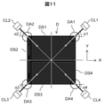
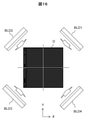
次に、表面検査の照明について図11、12を用いて説明する。図11はダイクラック検査用照明装置の配置を示す平面図である。図12はダイクラック検査用照明装置およびダイ認識用照明装置の配置を示す配置図である。 Next, the lighting for surface inspection will be described with reference to FIGS. 11 and 12. FIG. 11 is a plan view showing the arrangement of the lighting device for die crack inspection. FIG. 12 is a layout diagram showing the arrangement of the lighting device for die crack inspection and the lighting device for die recognition.
図11に示すように、ダイDのクラックを検査するためのダイクラック検査用照明装置CL1~CL4はダイDの隅付近からダイDの中心付近に照明が入射するように配置される。ダイDの四辺をX軸方向またはY軸方向に沿って配置する場合、ダイクラック検査用照明装置CL1~CL4の水平方向の照明の入射方向とX軸方向となす角度をそれぞれα1、α2、α3、α4とすると、0度<α1、α2、α3、α4<90度であり、α1≒α2≒α3≒α4≒45度が好ましい。図11では、ダイクラック検査用照明装置を四箇所に配置しているが一箇所でも二箇所でも三箇所でもよい。垂直方向の照明の入射角度(θ)は5~85度が好ましい。 As shown in FIG. 11, the die crack inspection lighting devices CL1 to CL4 for inspecting cracks in the die D are arranged so that the illumination is incident from the vicinity of the corner of the die D to the vicinity of the center of the die D. When the four sides of the die D are arranged along the X-axis direction or the Y-axis direction, the angles formed by the incident direction and the X-axis direction of the horizontal illumination of the die crack inspection lighting devices CL1 to CL4 are α1, α2, and α3, respectively. , Α4, 0 degrees <α1, α2, α3, α4 <90 degrees, and α1 ≈ α2 ≈ α3 ≈ α4 ≈ 45 degrees is preferable. In FIG. 11, the lighting devices for die crack inspection are arranged at four places, but may be one place, two places, or three places. The incident angle (θ) of the vertical illumination is preferably 5 to 85 degrees.
ダイDは、平面視で、X方向に延在する第一辺DS1および第三辺DS3と、Y方向に延在する第二辺DS2および第四辺DS4と、を有する。第一辺DS1と第三辺DS3とは対向し、第二辺DS2と第四辺DS4とは対向する。第一辺DS1と第四辺DS4とは角を形成し、その角を含む所定領域を第一角部DA1という。第二辺DS2と第一辺DS1とは角を形成し、その角を含む所定領域を第二角部DA2という。第三辺DS3と第二辺DS2とは角を形成し、その角を含む所定領域を第三角部DA3という。第四辺DS4と第三辺DS3とは角を形成し、その角を含む所定領域を第四角部DA4という。図11ではダイDが正方形であるので、照明装置CL1~CL4からの入射光はダイDの角を通過しているが、長方形ではあればその角を通過しない。ただし、第一角部DA1、第二角部DA2、第三角部DA3および第四角部DA4は所定の大きさの領域であり、照明装置CL1~CL4からの入射光は第一角部DA1、第二角部DA2、第三角部DA3および第四角部DA4を通過する。 The die D has a first side DS1 and a third side DS3 extending in the X direction, and a second side DS2 and a fourth side DS4 extending in the Y direction in a plan view. The first side DS1 and the third side DS3 face each other, and the second side DS2 and the fourth side DS4 face each other. A corner is formed between the first side DS1 and the fourth side DS4, and a predetermined region including the corner is referred to as a first corner portion DA1. The second side DS2 and the first side DS1 form a corner, and a predetermined region including the corner is referred to as a second corner portion DA2. A corner is formed between the third side DS3 and the second side DS2, and a predetermined region including the corner is referred to as a third triangular portion DA3. The fourth side DS4 and the third side DS3 form a corner, and a predetermined region including the corner is referred to as a fourth corner portion DA4. In FIG. 11, since the die D is square, the incident light from the lighting devices CL1 to CL4 passes through the corner of the die D, but if it is rectangular, it does not pass through the corner. However, the first corner portion DA1, the second corner portion DA2, the third triangular portion DA3 and the fourth corner portion DA4 are regions of a predetermined size, and the incident light from the lighting devices CL1 to CL4 is the first corner portion DA1. It passes through the second corner portion DA2, the third triangular portion DA3 and the fourth corner portion DA4.
図12に示すように、ダイDの位置決めまたは位置検査を行うためにダイDを認識するダイ認識用照明装置RL1~RL4はダイDの四辺のそれぞれと対向する位置に配置される。X軸方向に沿った辺に対向して配置されるダイ認識用照明装置RL1、RL3からの水平方向の照明の入射方向はY軸方向であり、Y軸方向に沿った辺に対向して配置されるダイ認識用照明装置RL2、RL4からの水平方向の照明の入射方向はX軸方向である。 As shown in FIG. 12, the die recognition illuminating devices RL1 to RL4 that recognize the die D in order to position or inspect the position of the die D are arranged at positions facing each of the four sides of the die D. The incident direction of the horizontal illumination from the die recognition illuminating devices RL1 and RL3 arranged facing the sides along the X-axis direction is the Y-axis direction, and they are arranged facing the sides along the Y-axis direction. The incident direction of the horizontal illumination from the die recognition illumination devices RL2 and RL4 is the X-axis direction.
完全な鏡面反射でないウェハ表面は、光の入射方向によっては、明視野となってしまうが、ウェハ表面加工はX軸方向およびY軸方向に準じるものが多く、ウェハの加工方向に対し、光の入射方向をX軸方向およびY軸方向に平行または垂直ではない領域に絞ると、垂直方向の入射角をどの角度にしても、ウェハ表面がカメラの光軸方向に光を反射させることはない。これにより、ウェハの表面状態に依存せず、暗視野を安定的に確保できる。 The wafer surface that is not completely mirror-reflected has a bright field depending on the incident direction of light, but the wafer surface processing often follows the X-axis direction and the Y-axis direction, and the light is applied to the processing direction of the wafer. When the incident direction is narrowed down to a region that is not parallel or perpendicular to the X-axis direction and the Y-axis direction, the wafer surface does not reflect light in the optical axis direction of the camera regardless of the angle of incidence in the vertical direction. As a result, a dark field can be stably secured without depending on the surface condition of the wafer.
<変形例>
以下、代表的な変形例について、幾つか例示する。以下の変形例の説明において、上述の実施例にて説明されているものと同様の構成および機能を有する部分に対しては、上述の実施例と同様の符号が用いられ得るものとする。そして、かかる部分の説明については、技術的に矛盾しない範囲内において、上述の実施例における説明が適宜援用され得るものとする。また、上述の実施例の一部、および、複数の変形例の全部または一部が、技術的に矛盾しない範囲内において、適宜、複合的に適用され得る。
<Modification example>
Hereinafter, some typical modifications will be illustrated. In the following description of the modified example, the same reference numerals as those in the above-described embodiment may be used for the portions having the same configuration and function as those described in the above-described embodiment. As for the explanation of such a portion, the explanation in the above-described embodiment can be appropriately incorporated within a technically consistent range. In addition, a part of the above-mentioned embodiment and all or a part of the plurality of modifications can be appropriately and combinedly applied within a technically consistent range.
(変形例1)
図13は変形例1に係る照明装置を示す模式斜視図である。図14は図13の照明装置を回転させる手段を示す模式斜視図である。図15は図13の照明装置で位置認識を行う場合の配置を示す模式平面図である。図16は図3の照明装置でダイクラック検査を行う場合の配置を示す模式平面図である。
(Modification 1)
FIG. 13 is a schematic perspective view showing the lighting device according to the first modification. FIG. 14 is a schematic perspective view showing a means for rotating the lighting device of FIG. 13. FIG. 15 is a schematic plan view showing an arrangement when position recognition is performed by the lighting device of FIG. FIG. 16 is a schematic plan view showing an arrangement when a die crack inspection is performed with the lighting device of FIG.
実施例の場合、ダイ認識用照明装置とは別にダイクラック検査用照明装置を配置したが、図13に示すように、変形例1では、ダイDの位置決めまたは位置検査(以下、位置認識と総称する。)を行う場合、バータイプの斜光照明装置(斜光バー照明装置)をダイDの四辺に対向するように配置し、ダイDのクラックの検査を行う場合、斜光バー照明装置を回転させてダイDの四隅に配置する。 In the case of the embodiment, the lighting device for die crack inspection is arranged separately from the lighting device for die recognition, but as shown in FIG. 13, in the modified example 1, the positioning or position inspection of the die D (hereinafter collectively referred to as position recognition). In the case of performing Place it at the four corners of the die D.
図14に示すように、制御部8により制御される照明装置の駆動部は、斜光バー照明装置BLD1~BLD4を取り付けた回転リング91と、回転リング91を支持する固定リング92と、固定リング92を支持する支柱93、94を備える。回転リング91はモータ95で駆動されるベルト96により固定リング92外側を回転する。これにより、斜光バー照明装置BLD1~BLD4は水平方向に回転することができる。
As shown in FIG. 14, the driving unit of the lighting device controlled by the control unit 8 includes a
図15に示すように、ダイDの位置認識を行う場合、斜光バー照明装置BLD1、BLD3からの照射光はY軸方向に沿ってダイDの中心に向かい、斜光バー照明装置BLD2、BLD4からの照射光はX軸方向に沿ってダイDの中心に向かう。 As shown in FIG. 15, when the position of the die D is recognized, the irradiation light from the oblique light bar illumination devices BLD1 and BLD3 is directed toward the center of the die D along the Y-axis direction, and is emitted from the oblique light bar illumination devices BLD2 and BLD4. The irradiation light is directed toward the center of the die D along the X-axis direction.
図16に示すように、ダイDのクラックの検査を行う場合、斜光バー照明装置BLD1、BLD2、BLD3、BLD4からの照射光はX軸方向からY軸方向に45度回転した方向からダイDの中心に向かう。 As shown in FIG. 16, when inspecting the crack of the die D, the irradiation light from the oblique bar lighting devices BLD1, BLD2, BLD3, and BLD4 is the direction of the die D rotated 45 degrees from the X-axis direction to the Y-axis direction. Head to the center.
ダイDのクラックの検査を行う場合、斜光バー照明装置の配置をウェハの加工方向から45度回転させた位置に配置したが、45度に限定されるものではなく、照射光がX軸方向およびY軸方向に沿わない方向に進行する角度であればよい。 When inspecting cracks in the die D, the oblique bar lighting device was placed at a position rotated 45 degrees from the processing direction of the wafer, but it is not limited to 45 degrees, and the irradiation light is in the X-axis direction and. Any angle may be used as long as it travels in a direction that does not follow the Y-axis direction.
(変形例2)
変形例2に係る照明装置について図17~19を用いて説明する。
(Modification 2)
The lighting device according to the second modification will be described with reference to FIGS. 17 to 19.
図17は変形例2に係る照明装置を示す模式斜視図である。図18は図17の照明装置の点灯、消灯を制御する手段を示す模式斜視図である。図19は図17の照明装置の点灯、消灯位置を説明する模式平面図である。 FIG. 17 is a schematic perspective view showing the lighting device according to the second modification. FIG. 18 is a schematic perspective view showing a means for controlling lighting and extinguishing of the lighting device of FIG. FIG. 19 is a schematic plan view illustrating the lighting and extinguishing positions of the lighting device of FIG.
実施例および変形例1の場合、斜光バー照明装置を用いたが、変形例2では、図17に示すようにリングタイプの斜光照明装置(斜光リング照明装置)RLDを用い、斜線部の領域R1~R4を点灯および消灯して位置認識およびクラックの検査を行う。斜光リング照明装置はクラック検査を行うとき、ウェハの加工方向に対し、X軸方向およびY軸方向からの照射を消灯する。 In the case of the embodiment and the modified example 1, the oblique light bar illumination device was used, but in the modified example 2, a ring type oblique light illumination device (oblique light ring illumination device) RLD was used as shown in FIG. 17, and the area R1 in the shaded area was used. -R4 is turned on and off to perform position recognition and crack inspection. When performing a crack inspection, the oblique light ring illuminator turns off the irradiation from the X-axis direction and the Y-axis direction with respect to the processing direction of the wafer.
図18に示すように、制御部8に制御される照明装置の制御部は、斜光リング照明装置RLDの領域R1~R4の点灯/消灯を制御する第一電源制御ボックス97_1と、斜光リング照明装置RLDの領域R1~R4と第一電源制御ボックス97_1を接続する電源ケーブル98_1と、斜光リング照明装置RLDの領域R5~R8の点灯/消灯を制御する第二電源制御ボックス97_2と、斜光リング照明装置RLDの領域R5~R8と第二電源制御ボックス97_2を接続する電源ケーブル98_2と、を備える。 As shown in FIG. 18, the control unit of the lighting device controlled by the control unit 8 includes a first power supply control box 97_1 for controlling lighting / extinguishing of areas R1 to R4 of the oblique light ring illumination device RLD, and an oblique light ring illumination device. A power cable 98_1 for connecting the RLD areas R1 to R4 and the first power supply control box 97_1, a second power supply control box 97_1 for controlling lighting / extinguishing of the oblique light ring lighting devices RLD areas R5 to R8, and an oblique light ring lighting device. A power cable 98_2 for connecting the regions R5 to R8 of the RLD and the second power supply control box 97_2 is provided.
図19に示すように、ダイDの位置認識を行う場合、斜光リング照明装置RLDのすべての領域R1~R8を点灯し、照射光がダイDに向かう。よって、斜光リング照明装置RLDからX軸方向およびY軸方向に沿ってダイDの中心に向かう照射光が存在する。 As shown in FIG. 19, when the position of the die D is recognized, all the areas R1 to R8 of the oblique light ring illumination device RLD are turned on, and the irradiation light is directed to the die D. Therefore, there is irradiation light directed from the oblique light ring illumination device RLD toward the center of the die D along the X-axis direction and the Y-axis direction.
ダイDのクラックの検査を行う場合、斜光リング照明装置RLDの領域R1~R4を消灯し領域R5~R8を点灯し、領域R5~R8からの照射光がダイDに向かう。領域R1~R4はX軸方向またはY軸方向と交差する領域であり、それぞれ斜光リング照明装置RLD全体の1/8の大きさの領域である。領域R5~R8はX軸方向とY軸方向との中間方向と交差する領域であり、それぞれ斜光リング照明装置RLD全体の1/8の大きさの領域である。よって、斜光リング照明装置RLDからの照射光はX軸方向からY軸方向に45度回転した領域からダイDの中心に向かい、斜光リング照明装置RLDからX軸方向およびY軸方向に沿ってダイDの中心に向かう照射光が存在しない。 When inspecting the crack of the die D, the regions R1 to R4 of the oblique light ring lighting device RLD are turned off, the regions R5 to R8 are turned on, and the irradiation light from the regions R5 to R8 is directed to the die D. The regions R1 to R4 are regions that intersect the X-axis direction or the Y-axis direction, and are regions having a size of 1/8 of the entire oblique light ring illuminating device RLD, respectively. The regions R5 to R8 are regions that intersect the intermediate direction between the X-axis direction and the Y-axis direction, and are regions having a size of 1/8 of the entire oblique light ring illuminating device RLD, respectively. Therefore, the irradiation light from the oblique light ring illuminating device RLD is directed toward the center of the die D from the region rotated 45 degrees from the X-axis direction to the Y-axis direction, and the die is directed from the oblique light ring illuminating device RLD along the X-axis direction and the Y-axis direction. There is no irradiation light toward the center of D.
本変形例では、領域R1~R4はそれぞれ斜光リング照明装置RLD全体の1/8の大きさの領域を示しているが1/8に限定されるものではなく、例えばボンディングされるダイが小さい場合には、領域R1~R4を1/8よりも大きくし、領域R5~R8を1/8よりも小さくしてより狭い領域で照射してもよい。 In this modification, the regions R1 to R4 each indicate a region having a size of 1/8 of the entire oblique light ring illuminating device RLD, but are not limited to 1/8, for example, when the die to be bonded is small. The regions R1 to R4 may be made larger than 1/8, and the regions R5 to R8 may be made smaller than 1/8 to irradiate in a narrower region.
クラックの外観検査は、ダイ位置認識を行う場所であるダイ供給部、中間ステージ、およびボンディングステージの少なくとも1か所で行うが、すべての箇所で行うのがより好ましい。ダイ供給部で行えば、早くクラックを検出することができる。中間ステージに行えば、ダイ供給部で検出できなかったクラックまたはピックアップ工程以降で発生したクラック(ボンディング工程よりも前に顕在化しなかったクラック)をボンディング前に検出することができる。また、ボンディングステージに行えば、ダイ供給部および中間ステージで検出できなかったクラック(ボンディング工程よりも前に顕在化しなかったクラック)またはボンディング工程以降で発生したクラックを、次のダイを積層するボンディング前に、または基板排出前に検出することができる。 The appearance inspection of the crack is performed at at least one place of the die supply part, the intermediate stage, and the bonding stage where the die position recognition is performed, but it is more preferable to perform the inspection at all the places. If it is done in the die supply section, cracks can be detected quickly. If the intermediate stage is performed, cracks that could not be detected in the die supply unit or cracks that occurred after the pickup process (cracks that did not become apparent before the bonding process) can be detected before bonding. Further, if the bonding stage is performed, cracks that could not be detected in the die supply section and the intermediate stage (cracks that did not become apparent before the bonding process) or cracks generated after the bonding process are bonded by laminating the next die. It can be detected before or before the substrate is ejected.
以上、本発明者によってなされた発明を実施例および変形例に基づき具体的に説明したが、本発明は、上記実施例および変形例に限定されるものではなく、種々変更可能であることはいうまでもない。 Although the invention made by the present inventor has been specifically described above based on Examples and Modifications, the present invention is not limited to the above Examples and Modifications, and can be variously modified. Not to mention.
例えば、変形例1では斜光バー照明装置を回転させることを説明したが、これに限定されるものではなく、ダイを回転してもよい。例えば、ダイが載置された中間ステージを回転して照射方向を変えてもよい。
また、実施例ではダイ位置認識の後にダイ外観検査認識を行っているが、ダイ外観検査認識の後にダイ位置認識を行ってもよい。
また、実施例ではウェハの裏面にDAFが貼付されているが、DAFはなくてもよい。
また、実施例ではピックアップヘッドおよびボンディングヘッドをそれぞれ1つ備えているが、それぞれ2つ以上であってもよい。また、実施例では中間ステージを備えているが、中間ステージがなくてもよい。この場合、ピックアップヘッドとボンディングヘッドは兼用してもよい。
また、実施例ではダイの表面を上にしてボンディングされるが、ダイをピックアップ後ダイの表裏を反転させて、ダイの裏面を上にしてボンディングしてもよい。この場合、中間ステージは設けなくてもよい。この装置はフリップチップボンダという。
また、実施例ではボンディングヘッドを備えるが、ボンディングヘッドがなくてもよい。この場合は、ピックアップされたダイは容器等に載置される。この装置はピックアップ装置という。
For example, in the first modification, the rotation of the oblique bar lighting device has been described, but the present invention is not limited to this, and the die may be rotated. For example, the irradiation direction may be changed by rotating the intermediate stage on which the die is placed.
Further, in the embodiment, the die appearance inspection recognition is performed after the die position recognition, but the die position recognition may be performed after the die appearance inspection recognition.
Further, in the embodiment, the DAF is attached to the back surface of the wafer, but the DAF may not be present.
Further, in the embodiment, one pickup head and one bonding head are provided, but two or more of each may be provided. Further, although the intermediate stage is provided in the embodiment, the intermediate stage may not be provided. In this case, the pickup head and the bonding head may be used in combination.
Further, in the embodiment, the bonding is performed with the front surface of the die facing up, but after picking up the die, the front and back surfaces of the die may be inverted and the back surface of the die may be facing up for bonding. In this case, the intermediate stage may not be provided. This device is called a flip chip bonder.
Further, although the bonding head is provided in the embodiment, the bonding head may not be provided. In this case, the picked-up die is placed in a container or the like. This device is called a pickup device.
10・・・ダイボンダ
1・・・ダイ供給部
13・・・突上げユニット
2・・・ピックアップ部
24・・・ウェハ認識カメラ
3・・・アライメント部
31・・・中間ステージ
32・・・ステージ認識カメラ
4・・・ボンディング部
41・・・ボンディングヘッド
42・・・コレット
44・・・基板認識カメラ
5・・・搬送部
51・・・基板搬送爪
8・・・制御部
9・・・基板
BS・・・ボンディングステージ
D・・・ダイ
P・・・パッケージエリア
CL1、CL2、CL3、CL4・・・クラック検出用照明装置
RL1、RL2、RL3、RL4・・・ダイ認識用照明装置
BLD1、BLD2、BLD3、BLD4・・・斜光バー照明装置
RLD・・・斜光リング照明装置
10 ... Die
Claims (12)
前記ダイを前記撮像装置の光学系軸に対して斜めから照明する照明装置と、
前記撮像装置および前記照明装置を制御する制御装置と、
を備え、
前記照明装置は、前記第一辺の中央から前記ダイの中心に向かう第一方向と、前記第二辺の中央から前記ダイの中心に向かう第二方向と、前記第三辺の中央から前記ダイの中心に向かう第三方向と、前記第四辺の中央から前記ダイの中心に向かう第四方向と、前記第一辺と前記第四辺とで形成する角を含む第一角部から前記ダイの中心に向かう第五方向と、前記第二辺と前記第一辺とで形成する角を含む第二角部から前記ダイの中心に向かう第六方向と、前記第三辺と前記第二辺とで形成する角を含む第三角部から前記ダイの中心に向かう第七方向と、前記第四辺と前記第三辺とで形成する角を含む第四角部から前記ダイの中心に向かう第八方向と、から照明することが可能であり、
前記制御装置は、
前記ダイの位置を認識する場合、前記照明装置で前記第一方向と前記第二方向と前記第三方向と前記第四方向とから照明して、前記撮像装置で前記ダイを撮像し、
前記ダイのクラックを検査する場合、前記照明装置で前記第一方向と前記第二方向と前記第三方向と前記第四方向とからの照明を抑え、前記第五方向と前記第六方向と前記第七方向と前記第八方向とから照明して、前記撮像装置で前記ダイを撮像するよう構成される
半導体製造装置。 An image pickup device that images a die having a first side, a second side connected to the first side, a third side facing the first side, and a fourth side facing the second side.
A lighting device that illuminates the die at an angle with respect to the optical system axis of the image pickup device, and
A control device that controls the image pickup device and the lighting device,
Equipped with
The lighting device has a first direction from the center of the first side toward the center of the die, a second direction from the center of the second side toward the center of the die, and a center of the third side to the die. From the first corner including the corner formed by the third direction toward the center, the fourth direction from the center of the fourth side toward the center of the die, and the first side and the fourth side. The fifth direction toward the center of the die, the sixth direction from the second corner including the angle formed by the second side and the first side toward the center of the die, the third side and the second side. The seventh direction from the third triangular portion including the corner formed by the sides toward the center of the die, and the fourth direction including the corner formed by the fourth side and the third side toward the center of the die. It is possible to illuminate from the eighth direction,
The control device is
When recognizing the position of the die, the lighting device illuminates the die from the first direction, the second direction, the third direction, and the fourth direction, and the image pickup device images the die.
When inspecting cracks in the die, the lighting device suppresses illumination from the first direction, the second direction, the third direction, and the fourth direction, and the fifth direction, the sixth direction, and the above. A semiconductor manufacturing apparatus configured to image the die with the image pickup device by illuminating from the seventh direction and the eighth direction .
前記照明装置は、
前記第一辺と対向する位置に配置される第一ダイ認識用照明装置と、
前記第二辺と対向する位置に配置される第二ダイ認識用照明装置と、
前記第三辺と対向する位置に配置される第三ダイ認識用照明装置と、
前記第四辺と対向する位置に配置される第四ダイ認識用照明装置と、
前記第一角部と対向する位置に配置される第一ダイクラック検査用照明装置と、
前記第二角部と対向する位置に配置される第二ダイクラック検査用照明装置と、
前記第三角部と対向する位置に配置される第三ダイクラック検査用照明装置と、
前記第四角部と対向する位置に配置される第四ダイクラック検査用照明装置と、
を備え、
前記制御装置は、
前記ダイの位置を認識する場合、前記第一ダイ認識用照明装置で前記第一方向から照明し、前記第二ダイ認識用照明装置で前記第二方向から照明し、前記第三ダイ認識用照明装置で前記第三方向から照明し、前記第四ダイ認識用照明装置で前記第四方向から照明して、前記撮像装置で前記ダイを撮像し、
前記ダイのクラックを検査する場合、前記第一ダイクラック検査用照明装置で前記第五方向から照明し、前記第二ダイクラック検査用照明装置で前記第六方向から照明し、前記第三ダイクラック検査用照明装置で前記第七方向から照明し、前記第四ダイクラック検査用照明装置で前記第八方向から照明して、前記撮像装置で前記ダイを撮像するよう構成される
半導体製造装置。 In claim 1 ,
The lighting device is
A first die recognition lighting device arranged at a position facing the first side,
A second die recognition lighting device arranged at a position facing the second side,
A lighting device for recognizing a third die, which is arranged at a position facing the third side,
A fourth die recognition lighting device arranged at a position facing the fourth side, and
A lighting device for inspection of a first die crack, which is arranged at a position facing the first corner portion,
A second die crack inspection lighting device arranged at a position facing the second corner portion,
A third die crack inspection lighting device arranged at a position facing the third triangular portion,
A fourth die crack inspection lighting device arranged at a position facing the fourth square portion, and a lighting device for inspection.
Equipped with
The control device is
When recognizing the position of the die, the lighting device for recognizing the first die illuminates from the first direction, the illuminating device for recognizing the second die illuminates from the second direction, and the lighting for recognizing the third die. The device illuminates from the third direction, the fourth die recognition illuminating device illuminates from the fourth direction, and the image pickup device images the die.
When inspecting a crack in the die, the first die crack inspection lighting device illuminates from the fifth direction, the second die crack inspection lighting device illuminates from the sixth direction, and the third die crack is inspected. A semiconductor manufacturing apparatus configured to illuminate from the seventh direction with an inspection illuminating device, illuminate from the eighth direction with the fourth die crack inspection illuminating device, and image the die with the image pickup device.
前記照明装置は、
第一斜光バー照明装置と、
第二斜光バー照明装置と、
第一斜光バー照明装置と対向して配置される第三斜光バー照明装置と、
第二斜光バー照明装置と対向して配置される第四斜光バー照明装置と、
を備え、
前記制御装置は、
前記ダイの位置を認識する場合、
前記第一斜光バー照明装置で前記第一方向から照明し、前記第二斜光バー照明装置で前記第二方向から照明し、前記第三斜光バー照明装置で前記第三方向から照明し、前記第四斜光バー照明装置で前記第四方向から照明して、前記撮像装置で前記ダイを撮像し、
前記ダイのクラックを検査する場合、
前記第一斜光バー照明装置で前記第五方向から照明し、前記第二斜光バー照明装置で前記第六方向から照明し、前記第三斜光バー照明装置で前記第七方向から照明し、前記第四斜光バー照明装置で前記第八方向から照明して、前記撮像装置で前記ダイを撮像するよう構成される
半導体製造装置。 In claim 1 ,
The lighting device is
The first oblique bar lighting device and
Second oblique bar lighting device and
The third oblique bar illuminator, which is placed facing the first oblique bar illuminator,
The fourth oblique bar illuminator, which is placed facing the second oblique bar illuminator,
Equipped with
The control device is
When recognizing the position of the die
The first oblique bar illuminating device illuminates from the first direction, the second oblique bar illuminating device illuminates from the second direction , and the third oblique bar illuminating device illuminates from the third direction . , The fourth oblique light bar illuminating device illuminates the die from the fourth direction , and the image pickup device images the die.
When inspecting cracks in the die
The first oblique bar illuminating device illuminates from the fifth direction, the second oblique bar illuminating device illuminates from the sixth direction , and the third oblique bar illuminating device illuminates from the seventh direction . A semiconductor manufacturing apparatus configured to illuminate the die from the eighth direction with the fourth oblique light bar illuminating device and to image the die with the imaging device.
前記照明装置は、第一領域と第二領域と第三領域と第四領域と第五領域と第六領域と第七領域と第八領域とを有する斜光リング照明装置であり、
前記制御装置は、
前記ダイの位置を認識する場合、
前記第一領域と前記第二領域と前記第三領域と前記第四領域と前記第五領域と前記第六領域と前記第七領域と前記第八領域とを点灯し、
前記第一領域で前記第一方向から照明し、前記第二領域で前記第二方向から照明し、前記第三領域で前記第三方向から照明し、前記第四領域で前記第四方向から照明し、前記第五領域で前記第五方向から照明し、前記第六領域で前記第六方向から照明し、前記第七領域で前記第七方向から照明し、前記第八領域で前記第八方向から照明して、前記撮像装置で前記ダイを撮像し、
前記ダイのクラックを検査する場合、
前記第一領域と前記第二領域と前記第三領域と前記第四領域とを消灯し、前記第五領域と前記第六領域と前記第七領域と前記第八領域とを点灯し、
前記第五領域で前記第五方向から照明し、前記第六領域で前記第六方向から照明し、前記第七領域で前記第七方向から照明し、前記第八領域で前記第八方向から照明して、前記撮像装置で前記ダイを撮像するよう構成される
半導体製造装置。 In claim 1 ,
The illuminating device is an oblique light ring illuminating device having a first region, a second region, a third region, a fourth region, a fifth region, a sixth region, a seventh region, and an eighth region.
The control device is
When recognizing the position of the die
The first region, the second region, the third region, the fourth region, the fifth region, the sixth region, the seventh region, and the eighth region are lit.
The first region is illuminated from the first direction , the second region is illuminated from the second direction , the third region is illuminated from the third direction , and the fourth region is illuminated from the third direction. Illuminated from the fourth direction, illuminated from the fifth direction in the fifth region, illuminated from the sixth direction in the sixth region, and illuminated from the seventh direction in the seventh region. Illuminate, illuminate from the eighth direction in the eighth region, and image the die with the image pickup device.
When inspecting cracks in the die
The first region, the second region, the third region, and the fourth region are turned off, and the fifth region, the sixth region, the seventh region, and the eighth region are turned on.
The fifth region is illuminated from the fifth direction, the sixth region is illuminated from the sixth direction , the seventh region is illuminated from the seventh direction , and the eighth region is illuminated from the seventh direction. A semiconductor manufacturing device configured to illuminate from eight directions and image the die with the image pickup device.
前記ダイが貼り付けられたダイシングテープを保持するウェハリングを有するダイ供給部を備え、
前記制御装置は前記撮像装置および前記照明装置を用いて前記ダイシングテープに貼り付けられたダイを撮像するよう構成される
半導体製造装置。 In claim 1, further
A die supply unit having a wafer ring for holding the dicing tape to which the die is attached is provided.
The control device is a semiconductor manufacturing device configured to image a die attached to the dicing tape by using the image pickup device and the lighting device.
前記ダイを基板または既にボンディングされているダイ上にボンディングするボンディングヘッドを備え、
前記制御装置は前記撮像装置および前記照明装置を用いて前記基板またはダイ上にボンディングされたダイを撮像するよう構成される
半導体製造装置。 In claim 1, further
A bonding head for bonding the die onto a substrate or a die that has already been bonded is provided.
The control device is a semiconductor manufacturing device configured to image a die bonded onto the substrate or die by using the image pickup device and the lighting device.
前記ダイをピックアップするピックアップヘッドと、
前記ピックアップされたダイが載置される中間ステージと、
を備え、
前記制御装置は前記撮像装置および前記照明装置を用いて前記中間ステージの上に載置されたダイを撮像するよう構成される
半導体製造装置。 In claim 1, further
The pickup head that picks up the die and
The intermediate stage on which the picked up die is placed and
Equipped with
The control device is a semiconductor manufacturing device configured to image a die mounted on the intermediate stage by using the image pickup device and the lighting device.
(b)ダイが貼付されたダイシングテープを保持するウェハリングを搬入する工程と、
(c)基板を搬入する工程と、
(d)前記ダイをピックアップする工程と、
(e)前記ピックアップしたダイを前記基板または既に前記基板にボンディングされているダイ上にボンディングする工程と、
を備える
半導体装置の製造方法。 (A) The step of preparing the semiconductor manufacturing apparatus according to any one of claims 1 to 4 .
(B) The process of carrying in the wafer ring that holds the dicing tape to which the die is attached, and
(C) The process of bringing in the substrate and
(D) The process of picking up the die and
(E) A step of bonding the picked-up die onto the substrate or a die that has already been bonded to the substrate.
A method for manufacturing a semiconductor device.
前記(d)工程は前記ピックアップされたダイを中間ステージに載置し、
前記(e)工程は前記中間ステージに載置されたダイをピックアップする
半導体装置の製造方法。 In claim 8 ,
In the step (d), the picked-up die is placed on an intermediate stage, and the picked-up die is placed on the intermediate stage.
The step (e) is a method for manufacturing a semiconductor device that picks up a die placed on the intermediate stage.
(f)前記(d)工程の前に、前記撮像装置および前記照明装置を用いて前記ダイの外観を検査する工程を備える
半導体装置の製造方法。 The method for manufacturing a semiconductor device according to claim 8 , further comprising (f) a step of inspecting the appearance of the die using the image pickup device and the lighting device before the step (d).
(g)前記(e)工程の後に、前記撮像装置および前記照明装置を用いて前記ダイの外観を検査する工程を備える
半導体装置の製造方法。 The method for manufacturing a semiconductor device according to claim 8 , further comprising (g) a step of inspecting the appearance of the die using the image pickup device and the lighting device after the step (e).
(h)前記(d)工程の後であって前記(e)工程の前に、前記撮像装置および前記照明装置を用いて前記ダイの外観を検査する工程を備える
半導体装置の製造方法。 The semiconductor device according to claim 9 , further comprising (h) a step of inspecting the appearance of the die using the image pickup device and the lighting device after the step (d) and before the step (e). Manufacturing method.
Priority Applications (4)
| Application Number | Priority Date | Filing Date | Title |
|---|---|---|---|
| JP2017178969A JP7010633B2 (en) | 2017-09-19 | 2017-09-19 | Semiconductor manufacturing equipment and methods for manufacturing semiconductor equipment |
| TW107130824A TWI678746B (en) | 2017-09-19 | 2018-09-03 | Semiconductor manufacturing device and method for manufacturing semiconductor device |
| KR1020180105215A KR102130386B1 (en) | 2017-09-19 | 2018-09-04 | Semiconductor manufacturing apparatus and method for manufacturing semiconductor device |
| CN201811090665.0A CN109524320B (en) | 2017-09-19 | 2018-09-18 | Semiconductor manufacturing apparatus and method for manufacturing semiconductor device |
Applications Claiming Priority (1)
| Application Number | Priority Date | Filing Date | Title |
|---|---|---|---|
| JP2017178969A JP7010633B2 (en) | 2017-09-19 | 2017-09-19 | Semiconductor manufacturing equipment and methods for manufacturing semiconductor equipment |
Publications (3)
| Publication Number | Publication Date |
|---|---|
| JP2019054203A JP2019054203A (en) | 2019-04-04 |
| JP2019054203A5 JP2019054203A5 (en) | 2020-08-13 |
| JP7010633B2 true JP7010633B2 (en) | 2022-01-26 |
Family
ID=65770976
Family Applications (1)
| Application Number | Title | Priority Date | Filing Date |
|---|---|---|---|
| JP2017178969A Active JP7010633B2 (en) | 2017-09-19 | 2017-09-19 | Semiconductor manufacturing equipment and methods for manufacturing semiconductor equipment |
Country Status (4)
| Country | Link |
|---|---|
| JP (1) | JP7010633B2 (en) |
| KR (1) | KR102130386B1 (en) |
| CN (1) | CN109524320B (en) |
| TW (1) | TWI678746B (en) |
Families Citing this family (4)
| Publication number | Priority date | Publication date | Assignee | Title |
|---|---|---|---|---|
| JP7151642B2 (en) * | 2019-06-28 | 2022-10-12 | 住友電気工業株式会社 | Surface emitting laser, its manufacturing method and its inspection method |
| JP7377655B2 (en) * | 2019-09-19 | 2023-11-10 | ファスフォードテクノロジ株式会社 | Die bonding equipment and semiconductor device manufacturing method |
| JP7437987B2 (en) | 2020-03-23 | 2024-02-26 | ファスフォードテクノロジ株式会社 | Die bonding equipment and semiconductor device manufacturing method |
| CN112992692B (en) * | 2021-05-19 | 2021-07-20 | 佛山市联动科技股份有限公司 | Method and system for full-automatic cutting of lead |
Citations (3)
| Publication number | Priority date | Publication date | Assignee | Title |
|---|---|---|---|---|
| JP2003185593A (en) | 2001-12-21 | 2003-07-03 | Nec Electronics Corp | Visual examination device for wafer |
| WO2005119227A1 (en) | 2004-06-04 | 2005-12-15 | Tokyo Seimitsu Co., Ltd. | Semiconductor appearance inspecting device and illuminating method |
| JP2017117916A (en) | 2015-12-24 | 2017-06-29 | ファスフォードテクノロジ株式会社 | Semiconductor manufacturing device, and method of manufacturing semiconductor device |
Family Cites Families (12)
| Publication number | Priority date | Publication date | Assignee | Title |
|---|---|---|---|---|
| JPS5538003A (en) * | 1978-09-08 | 1980-03-17 | Hitachi Ltd | Rectilinear pattern detecting device |
| TWI412736B (en) * | 2009-12-04 | 2013-10-21 | Delta Electronics Inc | A apparatus and method for inspecting inner defect of substrate |
| US8766192B2 (en) * | 2010-11-01 | 2014-07-01 | Asm Assembly Automation Ltd | Method for inspecting a photovoltaic substrate |
| WO2012081587A1 (en) * | 2010-12-14 | 2012-06-21 | 株式会社ニコン | Inspection method, inspection device, exposure management method, exposure system, and semiconductor device |
| JP5277266B2 (en) * | 2011-02-18 | 2013-08-28 | 株式会社日立ハイテクインスツルメンツ | Die bonder and semiconductor manufacturing method |
| JP2013197226A (en) * | 2012-03-19 | 2013-09-30 | Hitachi High-Tech Instruments Co Ltd | Die bonding method and die bonder |
| JP2014060249A (en) * | 2012-09-18 | 2014-04-03 | Hitachi High-Tech Instruments Co Ltd | Die bonder and die position recognition method |
| KR101431917B1 (en) * | 2012-12-27 | 2014-08-27 | 삼성전기주식회사 | examination apparatus of package |
| TWI570823B (en) * | 2013-08-14 | 2017-02-11 | 新川股份有限公司 | Semiconductor manufacturing apparatus and manufacturing method for semiconductor apparatus |
| WO2016088721A1 (en) * | 2014-12-05 | 2016-06-09 | 株式会社 アルバック | 822 substrate monitoring device and substrate monitoring method |
| JP6669523B2 (en) * | 2016-02-15 | 2020-03-18 | ファスフォードテクノロジ株式会社 | Die bonder and method of manufacturing semiconductor device |
| JP6683500B2 (en) * | 2016-02-24 | 2020-04-22 | 株式会社ディスコ | Inspection equipment and laser processing equipment |
-
2017
- 2017-09-19 JP JP2017178969A patent/JP7010633B2/en active Active
-
2018
- 2018-09-03 TW TW107130824A patent/TWI678746B/en active
- 2018-09-04 KR KR1020180105215A patent/KR102130386B1/en active IP Right Grant
- 2018-09-18 CN CN201811090665.0A patent/CN109524320B/en active Active
Patent Citations (3)
| Publication number | Priority date | Publication date | Assignee | Title |
|---|---|---|---|---|
| JP2003185593A (en) | 2001-12-21 | 2003-07-03 | Nec Electronics Corp | Visual examination device for wafer |
| WO2005119227A1 (en) | 2004-06-04 | 2005-12-15 | Tokyo Seimitsu Co., Ltd. | Semiconductor appearance inspecting device and illuminating method |
| JP2017117916A (en) | 2015-12-24 | 2017-06-29 | ファスフォードテクノロジ株式会社 | Semiconductor manufacturing device, and method of manufacturing semiconductor device |
Also Published As
| Publication number | Publication date |
|---|---|
| CN109524320A (en) | 2019-03-26 |
| JP2019054203A (en) | 2019-04-04 |
| CN109524320B (en) | 2023-03-24 |
| TW201929113A (en) | 2019-07-16 |
| KR102130386B1 (en) | 2020-07-06 |
| TWI678746B (en) | 2019-12-01 |
| KR20190032195A (en) | 2019-03-27 |
Similar Documents
| Publication | Publication Date | Title |
|---|---|---|
| TWI624887B (en) | Semiconductor manufacturing device and method for manufacturing semiconductor device | |
| KR102100889B1 (en) | Die bonding device and method of manufacturing semiconductor device | |
| JP7010633B2 (en) | Semiconductor manufacturing equipment and methods for manufacturing semiconductor equipment | |
| JP7102271B2 (en) | Semiconductor manufacturing equipment and manufacturing method of semiconductor equipment | |
| JP7029900B2 (en) | Manufacturing method of die bonding equipment and semiconductor equipment | |
| JP7225337B2 (en) | Semiconductor manufacturing equipment and semiconductor device manufacturing method | |
| JP2022098312A (en) | Die bonding device and manufacturing method of semiconductor device | |
| CN113436986B (en) | Chip mounting apparatus and method for manufacturing semiconductor device | |
| KR102304880B1 (en) | Semiconductor manufacturing apparatus and method for manufacturing semiconductor device | |
| TWI823297B (en) | Die bonding device and method for manufacturing semiconductor device | |
| JP2022026730A (en) | Manufacturing methods of die bonding device and semiconductor device |
Legal Events
| Date | Code | Title | Description |
|---|---|---|---|
| A521 | Request for written amendment filed |
Free format text: JAPANESE INTERMEDIATE CODE: A523 Effective date: 20200620 |
|
| A621 | Written request for application examination |
Free format text: JAPANESE INTERMEDIATE CODE: A621 Effective date: 20200620 |
|
| A977 | Report on retrieval |
Free format text: JAPANESE INTERMEDIATE CODE: A971007 Effective date: 20210520 |
|
| A131 | Notification of reasons for refusal |
Free format text: JAPANESE INTERMEDIATE CODE: A131 Effective date: 20210629 |
|
| A521 | Request for written amendment filed |
Free format text: JAPANESE INTERMEDIATE CODE: A523 Effective date: 20210819 |
|
| TRDD | Decision of grant or rejection written | ||
| A01 | Written decision to grant a patent or to grant a registration (utility model) |
Free format text: JAPANESE INTERMEDIATE CODE: A01 Effective date: 20211221 |
|
| A61 | First payment of annual fees (during grant procedure) |
Free format text: JAPANESE INTERMEDIATE CODE: A61 Effective date: 20220113 |
|
| R150 | Certificate of patent or registration of utility model |
Ref document number: 7010633 Country of ref document: JP Free format text: JAPANESE INTERMEDIATE CODE: R150 |