JP6980209B2 - Optical guide optical assembly - Google Patents
Optical guide optical assembly Download PDFInfo
- Publication number
- JP6980209B2 JP6980209B2 JP2018510950A JP2018510950A JP6980209B2 JP 6980209 B2 JP6980209 B2 JP 6980209B2 JP 2018510950 A JP2018510950 A JP 2018510950A JP 2018510950 A JP2018510950 A JP 2018510950A JP 6980209 B2 JP6980209 B2 JP 6980209B2
- Authority
- JP
- Japan
- Prior art keywords
- light
- optical
- guide
- diffractive
- diffraction
- Prior art date
- Legal status (The legal status is an assumption and is not a legal conclusion. Google has not performed a legal analysis and makes no representation as to the accuracy of the status listed.)
- Active
Links
Images


Classifications
-
- G—PHYSICS
- G02—OPTICS
- G02B—OPTICAL ELEMENTS, SYSTEMS OR APPARATUS
- G02B5/00—Optical elements other than lenses
- G02B5/18—Diffraction gratings
-
- G—PHYSICS
- G02—OPTICS
- G02B—OPTICAL ELEMENTS, SYSTEMS OR APPARATUS
- G02B6/00—Light guides; Structural details of arrangements comprising light guides and other optical elements, e.g. couplings
- G02B6/0001—Light guides; Structural details of arrangements comprising light guides and other optical elements, e.g. couplings specially adapted for lighting devices or systems
- G02B6/0011—Light guides; Structural details of arrangements comprising light guides and other optical elements, e.g. couplings specially adapted for lighting devices or systems the light guides being planar or of plate-like form
- G02B6/0013—Means for improving the coupling-in of light from the light source into the light guide
- G02B6/0015—Means for improving the coupling-in of light from the light source into the light guide provided on the surface of the light guide or in the bulk of it
- G02B6/0016—Grooves, prisms, gratings, scattering particles or rough surfaces
-
- G—PHYSICS
- G02—OPTICS
- G02B—OPTICAL ELEMENTS, SYSTEMS OR APPARATUS
- G02B27/00—Optical systems or apparatus not provided for by any of the groups G02B1/00 - G02B26/00, G02B30/00
- G02B27/0081—Optical systems or apparatus not provided for by any of the groups G02B1/00 - G02B26/00, G02B30/00 with means for altering, e.g. enlarging, the entrance or exit pupil
-
- G—PHYSICS
- G02—OPTICS
- G02B—OPTICAL ELEMENTS, SYSTEMS OR APPARATUS
- G02B27/00—Optical systems or apparatus not provided for by any of the groups G02B1/00 - G02B26/00, G02B30/00
- G02B27/01—Head-up displays
- G02B27/017—Head mounted
- G02B27/0172—Head mounted characterised by optical features
-
- G—PHYSICS
- G02—OPTICS
- G02B—OPTICAL ELEMENTS, SYSTEMS OR APPARATUS
- G02B27/00—Optical systems or apparatus not provided for by any of the groups G02B1/00 - G02B26/00, G02B30/00
- G02B27/10—Beam splitting or combining systems
-
- G—PHYSICS
- G02—OPTICS
- G02B—OPTICAL ELEMENTS, SYSTEMS OR APPARATUS
- G02B27/00—Optical systems or apparatus not provided for by any of the groups G02B1/00 - G02B26/00, G02B30/00
- G02B27/28—Optical systems or apparatus not provided for by any of the groups G02B1/00 - G02B26/00, G02B30/00 for polarising
-
- G—PHYSICS
- G02—OPTICS
- G02B—OPTICAL ELEMENTS, SYSTEMS OR APPARATUS
- G02B6/00—Light guides; Structural details of arrangements comprising light guides and other optical elements, e.g. couplings
-
- G—PHYSICS
- G02—OPTICS
- G02B—OPTICAL ELEMENTS, SYSTEMS OR APPARATUS
- G02B6/00—Light guides; Structural details of arrangements comprising light guides and other optical elements, e.g. couplings
- G02B6/0001—Light guides; Structural details of arrangements comprising light guides and other optical elements, e.g. couplings specially adapted for lighting devices or systems
- G02B6/0011—Light guides; Structural details of arrangements comprising light guides and other optical elements, e.g. couplings specially adapted for lighting devices or systems the light guides being planar or of plate-like form
- G02B6/0013—Means for improving the coupling-in of light from the light source into the light guide
- G02B6/0023—Means for improving the coupling-in of light from the light source into the light guide provided by one optical element, or plurality thereof, placed between the light guide and the light source, or around the light source
- G02B6/0028—Light guide, e.g. taper
-
- G—PHYSICS
- G02—OPTICS
- G02B—OPTICAL ELEMENTS, SYSTEMS OR APPARATUS
- G02B6/00—Light guides; Structural details of arrangements comprising light guides and other optical elements, e.g. couplings
- G02B6/0001—Light guides; Structural details of arrangements comprising light guides and other optical elements, e.g. couplings specially adapted for lighting devices or systems
- G02B6/0011—Light guides; Structural details of arrangements comprising light guides and other optical elements, e.g. couplings specially adapted for lighting devices or systems the light guides being planar or of plate-like form
- G02B6/0013—Means for improving the coupling-in of light from the light source into the light guide
- G02B6/0023—Means for improving the coupling-in of light from the light source into the light guide provided by one optical element, or plurality thereof, placed between the light guide and the light source, or around the light source
- G02B6/0031—Reflecting element, sheet or layer
-
- G—PHYSICS
- G02—OPTICS
- G02B—OPTICAL ELEMENTS, SYSTEMS OR APPARATUS
- G02B6/00—Light guides; Structural details of arrangements comprising light guides and other optical elements, e.g. couplings
- G02B6/0001—Light guides; Structural details of arrangements comprising light guides and other optical elements, e.g. couplings specially adapted for lighting devices or systems
- G02B6/0011—Light guides; Structural details of arrangements comprising light guides and other optical elements, e.g. couplings specially adapted for lighting devices or systems the light guides being planar or of plate-like form
- G02B6/0033—Means for improving the coupling-out of light from the light guide
- G02B6/0035—Means for improving the coupling-out of light from the light guide provided on the surface of the light guide or in the bulk of it
- G02B6/0038—Linear indentations or grooves, e.g. arc-shaped grooves or meandering grooves, extending over the full length or width of the light guide
-
- G—PHYSICS
- G02—OPTICS
- G02B—OPTICAL ELEMENTS, SYSTEMS OR APPARATUS
- G02B6/00—Light guides; Structural details of arrangements comprising light guides and other optical elements, e.g. couplings
- G02B6/0001—Light guides; Structural details of arrangements comprising light guides and other optical elements, e.g. couplings specially adapted for lighting devices or systems
- G02B6/0011—Light guides; Structural details of arrangements comprising light guides and other optical elements, e.g. couplings specially adapted for lighting devices or systems the light guides being planar or of plate-like form
- G02B6/0033—Means for improving the coupling-out of light from the light guide
- G02B6/005—Means for improving the coupling-out of light from the light guide provided by one optical element, or plurality thereof, placed on the light output side of the light guide
- G02B6/0055—Reflecting element, sheet or layer
-
- G—PHYSICS
- G02—OPTICS
- G02B—OPTICAL ELEMENTS, SYSTEMS OR APPARATUS
- G02B6/00—Light guides; Structural details of arrangements comprising light guides and other optical elements, e.g. couplings
- G02B6/0001—Light guides; Structural details of arrangements comprising light guides and other optical elements, e.g. couplings specially adapted for lighting devices or systems
- G02B6/0011—Light guides; Structural details of arrangements comprising light guides and other optical elements, e.g. couplings specially adapted for lighting devices or systems the light guides being planar or of plate-like form
- G02B6/0075—Arrangements of multiple light guides
-
- G—PHYSICS
- G02—OPTICS
- G02B—OPTICAL ELEMENTS, SYSTEMS OR APPARATUS
- G02B6/00—Light guides; Structural details of arrangements comprising light guides and other optical elements, e.g. couplings
- G02B6/24—Coupling light guides
- G02B6/26—Optical coupling means
- G02B6/34—Optical coupling means utilising prism or grating
-
- G—PHYSICS
- G02—OPTICS
- G02B—OPTICAL ELEMENTS, SYSTEMS OR APPARATUS
- G02B27/00—Optical systems or apparatus not provided for by any of the groups G02B1/00 - G02B26/00, G02B30/00
- G02B27/01—Head-up displays
- G02B27/0101—Head-up displays characterised by optical features
- G02B2027/0112—Head-up displays characterised by optical features comprising device for genereting colour display
- G02B2027/0116—Head-up displays characterised by optical features comprising device for genereting colour display comprising devices for correcting chromatic aberration
-
- G—PHYSICS
- G02—OPTICS
- G02B—OPTICAL ELEMENTS, SYSTEMS OR APPARATUS
- G02B27/00—Optical systems or apparatus not provided for by any of the groups G02B1/00 - G02B26/00, G02B30/00
- G02B27/01—Head-up displays
- G02B27/0101—Head-up displays characterised by optical features
- G02B2027/0123—Head-up displays characterised by optical features comprising devices increasing the field of view
- G02B2027/0125—Field-of-view increase by wavefront division
Description
本発明は、一般に光学アセンブリに関し、とりわけ、光学的開口の拡大に関係する。 The present invention relates generally to optical assemblies and, in particular, to the expansion of optical apertures.
図7のAを参照すると、導波路内で回折コンポーネントを使用する従来の光学的開口の拡大の大まかな略図が示されている。現在の図では、入射光(画像)はページの外からページまで垂直である。内連結(Coupling−in)要素(1001)は入射光を側方拡大要素(1002)へ連結し、側方拡大要素(1002)は光を側方に(現在の図で左から右まで)拡大する。その後、側方に拡大した光は垂直拡大要素(1003)へ連結して、垂直拡大要素(1003)は、光を垂直に(現在の図で上から下に)拡大し、その光をユーザー(ビューアーの目)に外連結する。 Referring to A in FIG. 7, a rough schematic representation of the enlargement of a conventional optical aperture using a diffractive component in a waveguide is shown. In the current figure, the incident light (image) is vertical from the outside of the page to the page. The coupling-in element (1001) connects the incident light to the lateral magnifying element (1002), and the lateral magnifying element (1002) magnifies the light laterally (from left to right in the current figure). do. The light magnified laterally is then connected to the vertical magnifying element (1003), which magnifies the light vertically (from top to bottom in the current figure) and directs the light to the user (1003). Externally connected to the viewer's eyes).
従来の回折素子は、様々な波長を備えた光線が様々な角度で回折する色分散を導入する。色分散を減らすために狭帯域光源(レーザーなど)を使用することができる。より現実的な解決策は、互いの分散を打ち消すために回折コンポーネントを設計することである。 Conventional diffraction elements introduce a color dispersion in which light rays having various wavelengths are diffracted at various angles. Narrowband light sources (such as lasers) can be used to reduce color dispersion. A more realistic solution is to design the diffraction components to cancel each other's dispersion.
図7のBを参照すると、角度領域(角度間隔)で伝播する光の図7のAの回折方向の図が示されている。破線の矢印と実線の矢印は2つの様々な典型的な波長を示す。領域(1005)の開始角度は、光線が光ガイドへ連結される第1の回折素子(内連結要素(1001))にぶつかるときの、光線の角度を表わす。領域(1007)は、内連結要素(1001)の後の光線の方向を表し、領域(1009)は側方拡大要素(1002)後の光線の方向を表し、および領域(1005)はさらに、垂直的拡大要素(1003)によって光ガイドからの連結後の光線の角度を表す。光ガイドに入る光線の方向は、色分散を最小限に抑えるために光ガイドから連結された光線の方向と等しい。光の様々な波長が光ガイド内に伝播すると、様々な波長は異なる方向を有し、光ガイドから出力されるときと同じ方向を有する。 Referring to B in FIG. 7, a diagram of the diffraction direction of A in FIG. 7 of light propagating in an angular region (angle interval) is shown. The dashed and solid arrows indicate two different typical wavelengths. The start angle of the region (1005) represents the angle of the light beam when it hits the first diffraction element (inner coupling element (1001)) connected to the light guide. The region (1007) represents the direction of the light beam after the inner connecting element (1001), the region (1009) represents the direction of the light beam after the lateral magnifying element (1002), and the region (1005) is further vertical. The magnifying element (1003) represents the angle of the ray after connection from the optical guide. The direction of the rays entering the light guide is equal to the direction of the rays connected from the light guide to minimize color dispersion. When different wavelengths of light propagate in the light guide, the different wavelengths have different directions, the same as when they are output from the light guide.
基礎技術
図1は従来の先行技術の折り畳み式の光学構造を例示し、ここで、基板(2)は表示源(4)により照射される。表示はコリメート光学系(6)(例えばレンズ)によってコリメートされる。表示源(4)からの光は、主な光線(11)が基板平面と平行になるように、第1の反射面(8)によって基板(2)へ連結される。第2の反射面(12)は、基板からビューアーの目(14)へ光を連結する。この構造はコンパクトであるにもかかわらず、著しい欠点に苛まされている。とりわけ、非常に制限されたFOVだけしか達成することができない。
Basic Techniques FIG. 1 illustrates a conventional prior art foldable optical structure, where the substrate (2) is illuminated by the display source (4). The display is collimated by collimating optical system (6) (eg, lens). The light from the display source (4) is connected to the substrate (2) by the first reflecting surface (8) so that the main light rays (11) are parallel to the substrate plane. The second reflective surface (12) connects light from the substrate to the viewer's eyes (14). Despite its compact size, this structure suffers from significant drawbacks. In particular, only very limited FOV can be achieved.
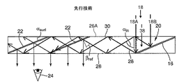
ここで、図2を参照すると、典型的な光誘導光学素子(LOE)の側面図が示されている。上記の制限を緩和するために、選択反射面のアレイを、光誘導光学素子(LOE)内で使用し、製造することができる。第1の反射面(16)は、デバイスの後ろに位置付けられる光源(図示せず)から発せられるコリメートされた表示光線(ビーム)(18)により照射される。図面の簡潔さのために、1つの光線、すなわち、入射光線(38)(「ビーム」あるいは「入射光線」とも呼ばれる)だけが一般に描かれている。ビーム(18A)と(18B)などの入射光の他の光線は、入射光瞳孔の左と右の縁などの入射瞳の縁を指定するために使用されることもある。一般に、画像が光線によって本明細書に表される場合はいつでも、光線は画像のサンプルビームであり、これは、画像の点またはピクセルに各々対応するわずかに異なる角度で複数のビームによって典型的に形成されることに注目されたい。特に画像の先端と呼ばれる場合を除いて、例示されるビームは典型的に画像の重心である。 Here, with reference to FIG. 2, a side view of a typical optical induction optical element (LOE) is shown. To alleviate the above limitations, an array of selective reflective surfaces can be used and manufactured within the optical induction optics (LOE). The first reflective surface (16) is illuminated by a collimated display beam (18) emitted from a light source (not shown) located behind the device. For the sake of simplicity in the drawings, only one ray, the incident ray (38) (also referred to as the "beam" or "incident ray"), is generally drawn. Other rays of incident light, such as the beams (18A) and (18B), may also be used to specify the edges of the entrance pupil, such as the left and right edges of the entrance light pupil. In general, whenever an image is represented herein by a ray, the ray is a sample beam of the image, which is typically by multiple beams at slightly different angles, each corresponding to a point or pixel in the image. Note that it is formed. Except as specifically referred to as the tip of the image, the illustrated beam is typically the center of gravity of the image.
反射面(16)は光源からの入射光を反射し、入射光は内部全反射によって光ガイド(20)の内部で捕捉される。光ガイド(20)は「導波路」、「平面基板」、および「光伝送基板」とも呼ばれる。光ガイド(20)は、後(主)面(26)と前(主)面(26A)として図面で示されている、互いに平行な少なくとも2つの(主)面を含む。光ガイド(20)が通常対称的である(したがって、主面(26)、(26A)への言及を取り替えても同じ結果をもたらすことができる)ため、主面(26)と(26A)に対して「前」および「後ろ」との指示は参照の利便性のためであることに留意されたい。光ガイド(20)は本明細書の文脈では1次元(1D)導波路と呼ばれ、1対の平行な面(この場合、主面(26)、(26A))の間の1つだけの寸法で注入された画像をガイドする。 The reflecting surface (16) reflects the incident light from the light source, and the incident light is captured inside the light guide (20) by internal total internal reflection. The optical guide (20) is also referred to as a "waveguide," "flat substrate," and "optical transmission board." The optical guide (20) includes at least two (main) planes parallel to each other, shown in the drawings as a rear (main) plane (26) and a front (main) plane (26A). Since the optical guides (20) are usually symmetrical (thus, replacing the references to the main surfaces (26), (26A) can produce the same result), the main surfaces (26) and (26A) Note that the "front" and "back" instructions, on the other hand, are for convenience of reference. The optical guide (20) is referred to herein as a one-dimensional (1D) waveguide and is only one between a pair of parallel planes (in this case, the main planes (26), (26A)). Guide the injected image in dimensions.
入射光線(38)は、基板の近位端(図の右側)で基板に入る。光は、光ガイドと1つ以上のファセット、通常少なくとも複数のファセット、および典型的にはいくつかのファセットを通って、光ガイドの遠位端(図の左側)に向かって伝播する。光は、伝播の当初の伝播方向(28)と別の伝播方向(30)の両方において光ガイドを通って伝播する。 The incident ray (38) enters the substrate at the proximal end of the substrate (on the right side of the figure). Light propagates through the optical guide and one or more facets, usually at least multiple facets, and typically several facets, toward the distal end of the optical guide (left side of the figure). Light propagates through the optical guide in both the initial propagation direction (28) and another propagation direction (30).
基板(20)の表面からいくつかの反射の後、捕捉された波は選択反射面(22)のアレイに達し、これが基板からの光をビューアーの目(24)へ連結する。代替的な構造では、選択反射面(22)は、光線(18)の直後に、基板(20)の表面から最初に反射することなく、基板に入る。 After some reflection from the surface of the substrate (20), the captured wave reaches an array of selective reflection planes (22), which directs the light from the substrate to the viewer's eyes (24). In an alternative structure, the selective reflective surface (22) enters the substrate immediately after the light beam (18) without first reflecting from the surface of the substrate (20).
選択反射面(22)などの内部の部分反射面は一般に本明細書の文脈では「ファセット」と呼ばれる。極限では、ファセットは、完全反射型(100%の反射率あるいはミラー、例えば、基板の遠位端における最後のファセット)、あるいは最小限反射型であり得る。現実用途の強化のために、ファセットは部分反射型であり、現実世界からの光が上部表面(26A)を介して入り、ファセットを含む基板を横断し、および、基板を出て下部表面(26)を介してビューアーの目(24)に至ることを可能にする。仮想現実用途のために、ファセットは100%の反射率を有する第1の内連結ミラーなどの代替的な反射率を有することもある。なぜなら、現実世界からの画像光はこのミラーを横断する必要はないからである。内部部分反射面(22)は一般に、光ガイド(20)の伸長の方向に対して斜角(つまり、平行でも垂直でもない)で光ガイド(20)を少なくとも部分的に横断する。 Internal partial reflective surfaces, such as the selective reflective surface (22), are commonly referred to as "facets" in the context of this specification. In the limit, the facet can be fully reflective (100% reflectance or mirror, eg, the last facet at the distal end of the substrate), or minimally reflective. For enhanced practical use, the facets are partially reflective, allowing light from the real world to enter through the upper surface (26A), traverse the substrate containing the facets, and exit the substrate to the lower surface (26A). ) Allows you to reach the viewer's eyes (24). For virtual reality applications, facets may also have an alternative reflectance, such as a first internally coupled mirror with 100% reflectance. This is because the image light from the real world does not have to cross this mirror. The internal partially reflective surface (22) generally traverses the light guide (20) at least partially at an oblique angle (ie, neither parallel nor perpendicular) to the direction of extension of the light guide (20).
反射率への言及は一般に名目上の反射率に関するものである。名目上の反射率は、基板中の特定位置で必要とされる全反射である。例えば、ファセットの反射率が50%と言及される場合、これは一般に名目上の反射率の50%を指す。名目上の反射率が10%である場合、50%の反射率は5%のファセットの反射率をもたらす。当業者は使用の文脈から反射率の割合の使用を理解するであろう。部分反射は、限定されないが、ある割合の光の伝送あるいは偏光の使用を含む、様々な技術によって実行可能である。 References to reflectance generally relate to nominal reflectance. Nominal reflectance is the total internal reflection required at a particular location in the substrate. For example, when facet reflectance is referred to as 50%, this generally refers to 50% of the nominal reflectance. If the nominal reflectance is 10%, then a reflectance of 50% results in a reflectance of 5% facet. Those skilled in the art will understand the use of reflectance percentages from the context of use. Partial reflection can be performed by a variety of techniques, including, but not limited to, the transmission of a proportion of light or the use of polarized light.
図3のAとBは、選択反射面の所望の反射率挙動を例示する。図3のAでは、光線(32)はファセット(34)から部分的に反射され、基板(20)から連結される(38B)。図3のBでは、光線(36)は顕著な反射なく、ファセット(34)を通って伝送される。 A and B in FIG. 3 illustrate the desired reflectance behavior of the selective reflective surface. In A of FIG. 3, the light beam (32) is partially reflected from the facet (34) and connected from the substrate (20) (38B). In FIG. 3B, the light beam (36) is transmitted through the facet (34) without significant reflection.
図4のAは、光を基板に連結し、その後、光をビューアーの目へ連結する、選択反射面のアレイの詳細な断面図である。図に示すように、光源(4)からの光線(38)は第1の部分反射面にぶつかる。光線(41)の一部はもともとの方向を継続し、基板から連結される。光線(42)の別の部分は内部全反射によって基板へ連結される。捕捉された光線は、点(44)で他の2つの部分反射面(22)によって基板から徐々に外連結される。第1の反射面(16)のコーティング特性は、他の反射面(22)、(46)のコーティング特性に必ずしも類似しなければならないというわけではない。このコーティングは、金属性、二色性、またはハイブリッドの金属−二色性の、より簡易なビームスプリッターであり得る。同様に、非シースルー(non−see−through)システムの場合、最後の反射面(46)は簡易なミラーであり得る。 FIG. 4A is a detailed cross-sectional view of an array of selective reflective surfaces connecting light to a substrate and then light to the viewer's eyes. As shown in the figure, the light ray (38) from the light source (4) hits the first partially reflecting surface. A portion of the light beam (41) continues in its original direction and is connected from the substrate. Another portion of the ray (42) is connected to the substrate by internal total internal reflection. The captured light beam is gradually externally connected from the substrate at the point (44) by the other two partially reflecting surfaces (22). The coating properties of the first reflective surface (16) do not necessarily have to be similar to the coating properties of the other reflective surfaces (22), (46). This coating can be a metallic, dichroic, or hybrid metal-dichroic, simpler beam splitter. Similarly, for non-see-through systems, the final reflective surface (46) can be a simple mirror.
図4のBは、反射面のアレイを含む装置の詳細な断面図であり、最後の反射面(46)が全反射ミラーである。最後の反射面(46)の最も左側の部分はこのような場合では光学的にアクティブではあり得ず、周辺光線(48)を基板から該連結することはできない。従って、デバイスの出力開口はわずかに小さくなる。しかしながら、光学効率ははるかに高くなり、LOEの製造プロセスははるかに簡素になり得る。 FIG. 4B is a detailed cross-sectional view of the device including an array of reflective surfaces, wherein the final reflective surface (46) is a total internal reflection mirror. The leftmost portion of the last reflective surface (46) cannot be optically active in such cases and the peripheral rays (48) cannot be said to be connected from the substrate. Therefore, the output aperture of the device is slightly smaller. However, the optical efficiency is much higher and the LOE manufacturing process can be much simpler.
図2で示された構造とは異なり、反射面(16)と(22)の配向に対する制約があるということに注目することは重要である。前の構造では、すべての光は反射面(16)によって基板の内部で連結される。従って、表面(16)は表面(22)と平行である必要はない。さらに、反射面は、光が入力波の方向とは正反対方向に基板から外連結されるように、配向されてもよい。図4のAで例示された構造については、しかしながら、入力光の一部は表面(16)によって反射されないが、入力光(38)のもともとの方向に継続して、直ちに出力光(41)として基板から外連結される。従って、同じ平面波から始まるすべての光線が同じ出力方向を確実に有するように、すべての反射面(22)が互いに平行でなければならないだけでなく、表面(16)も同様に表面(22)に対して平行でなければならない。 It is important to note that, unlike the structure shown in FIG. 2, there are restrictions on the orientation of the reflective surfaces (16) and (22). In the previous structure, all light is connected inside the substrate by a reflective surface (16). Therefore, the surface (16) does not have to be parallel to the surface (22). Further, the reflective surface may be oriented so that the light is externally connected from the substrate in the direction opposite to the direction of the input wave. For the structure illustrated in A of FIG. 4, however, some of the input light is not reflected by the surface (16), but continues in the original direction of the input light (38) and immediately as the output light (41). Externally connected from the substrate. Therefore, not only must all reflecting surfaces (22) be parallel to each other to ensure that all rays starting from the same plane wave have the same output direction, but the surface (16) is also on the surface (22). Must be parallel to each other.
再度、図4のAを参照すると、基板からの光を連結するための2つの反射面を有するシステムが示され、しかしながら、光学系の必要とされる出力開口と基板の厚さに従って任意の数の反射面を使用することができる。当然のことながら、1つの外連結面しか必要とされない場合がある。その場合、出力開口はシステムの入力開口のサイズの事実上2倍になる。最後の構造に必要とされる反射面だけは単純なビームスプリッターとミラーである。 Again, with reference to A in FIG. 4, a system with two reflective surfaces for connecting light from the substrate is shown, however, any number according to the required output aperture of the optical system and the thickness of the substrate. Reflective surface can be used. Of course, only one outer connecting surface may be required. In that case, the output aperture is effectively double the size of the input aperture of the system. The only reflective surface required for the final structure is a simple beam splitter and mirror.
本図に記載される装置において、表示源からの光は、基板の端部で基板へと連結されるが、対称システムを有することが好ましいシステムがある。すなわち、入力光は、基板の中央部で基板へと連結されるべきである。 In the apparatus described in this figure, the light from the display source is connected to the substrate at the end of the substrate, but there are systems in which it is preferable to have a symmetric system. That is, the input light should be connected to the substrate at the center of the substrate.
図4のCは、対称構造を有する側方の瞳孔拡張の一次元の(1D)光ガイドの詳細な断面図を例示するダイヤグラムである。本図は、対称な光モジュールを生成するために、2つの同一の基板を組み合わせる方法を例示している。見られるように、表示源(4)からの光の一部は、直接部分反射面を通り抜けて基板から出る。光の他の一部は、部分反射面(16R)および(16L)によって、それぞれ、基板の右側(20R)へと及び基板の左側(20L)へと連結される。その後、捕捉された光は、それぞれ、反射面(22R)および(22L)によって、徐々に外連結される。明らかに、出力開口は、システムの入力開口のサイズの3倍であり、図5のBに記載されている倍率と同じ倍率である。しかしながら、前のシステムとは異なり、ここでのシステムは、右および左の基板の接合面(29)を中心に対称である。 FIG. 4C is a diagram illustrating a detailed cross-sectional view of a one-dimensional (1D) optical guide of lateral pupil dilation with a symmetrical structure. This figure illustrates how to combine two identical substrates to produce a symmetric optical module. As can be seen, some of the light from the display source (4) passes directly through the partially reflective surface and exits the substrate. The other part of the light is connected to the right side (20R) of the substrate and to the left side (20L) of the substrate by the partially reflecting surfaces (16R) and (16L), respectively. The captured light is then gradually externally coupled by the reflective surfaces (22R) and (22L), respectively. Obviously, the output aperture is three times the size of the input opening of the system, which is the same magnification as shown in FIG. 5B. However, unlike the previous system, the system here is symmetrical about the junction surface (29) of the right and left substrates.
ここで図5のAおよびBを参照すると、光ガイドに加えて(on top of)図4のBおよびCの典型的な実装が示されている。図4のBおよびCの構成は、入射画像を横に拡大したものである。図4のBの装置は、図5のAの第1のLOE(20a)を実装するために使用され、図4のCの装置は、図5のBの第1のLOE(20a’)を実装するために使用され、および図2の装置は、第2のLOE(20b)を実装するために使用され得る。 Referring here to A and B of FIG. 5, a typical implementation of B and C of FIG. 4 is shown in addition to the optical guide (on top of). The configurations of B and C in FIG. 4 are laterally enlarged images of an incident image. The device B of FIG. 4 is used to implement the first LOE (20a) of A of FIG. 5, and the device C of FIG. 4 is a first LOE (20a') of B of FIG. Used for mounting, and the device of FIG. 2 can be used to mount a second LOE (20b).
図5のAは、二重のLOE構成を利用する2つの軸に沿ったビームを拡大するための代替方法を例示する。入力波(90)は、第1の反射面(16a)によって、図4のBにおいて例示された構造に類似した非対称の構造を有する、第1のLOE(20a)へと連結され、その後、η軸に沿って伝播する。部分反射面(22a)は、第1のLOE(20a)から出て光に連結し、その後、光は、反射面(16b)によって第2の非対称のLOE(20b)へと連結される。その後、光は、ξ軸に沿って伝播し、その後、選択反射面(22b)によって外連結される。示されるように、元のビーム(90)は両軸に沿って拡大され、ここで全体的な拡大は、要素(16a)および(22b)の横寸法間の比率によって判定される。図5のAで与えられた構成は、単に二重のLOEセットアップの一例である。また、複雑な光学システムを形成するために2つ以上のLOEが一緒に組み合わせられる他の構成も可能である。 A in FIG. 5 illustrates an alternative method for magnifying a beam along two axes utilizing a dual LOE configuration. The input wave (90) is connected by a first reflecting surface (16a) to a first LOE (20a) having an asymmetric structure similar to the structure exemplified in FIG. 4B, and then η. Propagate along the axis. The partially reflective surface (22a) exits the first LOE (20a) and is connected to the light, after which the light is connected by the reflecting surface (16b) to the second asymmetric LOE (20b). The light then propagates along the ξ axis and is then externally coupled by the selective reflection surface (22b). As shown, the original beam (90) is magnified along both axes, where the overall magnifying is determined by the ratio between the lateral dimensions of the elements (16a) and (22b). The configuration given in A of FIG. 5 is merely an example of a dual LOE setup. Other configurations are also possible in which two or more LOEs are combined together to form a complex optical system.
ここで図5のBを参照すると、二重のLOE構成を利用する2つの軸に沿ってビームを拡大するための別の方法を例示するダイヤグラムが示されている。通常、光が表面(16b)によって第2のLOE(20b)へと連結される領域は、外部光に対して透過性にはなり得ず、シースルー領域の一部ではない。したがって、第1のLOE(20a)は透過性である必要がない。結果として、シースルーのシステムに関してさえ、本図において見ることができるように、対称な構造を有するように第1のLOE(20a)を設計することは通常可能である。第2のLOE(20b)は、ユーザーが外部の様子を見ることを可能にする非対称の構造を有する。この構成では、入力ビーム(90)の一部は、元の方向(92)に沿って第2のLOE(20b)の内連結ミラー(16b)へと続き、一方で他の部分(94)は、反射面(16a)によって第1のLOE(20a’)へと連結し、η軸に沿って伝播し、その後、選択反射面(22a)によって第2のLOE(20b)へと連結される。その後、両方の部分は、反射面(16b)によって第2の非対称のLOE(20b)へと連結され、ξ軸に沿って伝播し、その後、選択反射面(22b)によって連結される。 Referring here to B in FIG. 5, a diagram illustrating another method for expanding the beam along two axes utilizing a dual LOE configuration is shown. Normally, the region where the light is connected to the second LOE (20b) by the surface (16b) cannot be transparent to external light and is not part of the see-through region. Therefore, the first LOE (20a) does not have to be transparent. As a result, even for see-through systems, it is usually possible to design the first LOE (20a) to have a symmetrical structure, as can be seen in this figure. The second LOE (20b) has an asymmetric structure that allows the user to see the outside world. In this configuration, part of the input beam (90) continues along the original direction (92) to the internally connected mirror (16b) of the second LOE (20b), while the other part (94). , Connected to the first LOE (20a') by the reflective surface (16a), propagated along the η axis, and then connected to the second LOE (20b) by the selective reflective surface (22a). Both portions are then connected by a reflective surface (16b) to a second asymmetric LOE (20b), propagated along the ξ axis, and then connected by a selective reflective surface (22b).
図6は、標準の眼鏡フレーム(107)に埋め込まれたLOE(20a)/(20a’)および(20b)の一例を例示している。表示源(4)、折り畳み式の光学系およびコリメート光学系(6)は、第2のLOE(20b)の縁部に位置する、LOE(20a)/(20a’)の真横の眼鏡フレームのアーム部分(112)の内部に組み立てられる。表示源が、小さなCRT、LCD、またはOLEDなどの、電子素子である場合については、表示源のための駆動電子機器(114)は、アーム(112)の後部部分の内部に組み立てられ得る。電源およびデータインターフェース(116)は、リード(118)、または無線または光の伝送を含む他の通信手段によってアーム(112)に接続可能である。代替的に、バッテリーおよび小型データリンク電子機器は、眼鏡フレームにおいて一体化され得る。本図は一例であり、表示源が、LOE平面と平行に、またはLOEの上部において取り付けられる、アセンブリを含む、他の考えられ得るヘッドマウントディスプレイの配置も構築され得る。 FIG. 6 illustrates an example of LOE (20a) / (20a') and (20b) embedded in a standard spectacle frame (107). The display source (4), the foldable optical system, and the collimating optical system (6) are located on the edge of the second LOE (20b) and are located on the arm of the spectacle frame directly beside the LOE (20a) / (20a'). Assembled inside the portion (112). If the display source is an electronic device such as a small CRT, LCD, or OLED, the drive electronics (114) for the display source may be assembled inside the rear portion of the arm (112). The power and data interface (116) can be connected to the arm (112) by a read (118), or other means of communication including wireless or optical transmission. Alternatively, the battery and small datalink electronics may be integrated in the spectacle frame. This figure is an example, and other possible head-mounted display arrangements, including assemblies, in which the display source is mounted parallel to the LOE plane or at the top of the LOE can also be constructed.
この基礎技術の追加の詳細は、米国特許第7,643,214号、および公開されておらず、本発明に対する先行技術を構成しないPCT/IL2018/050025において見られ得る。 Additional details of this basic art can be found in US Pat. No. 7,643,214, and PCT / IL2018 / 050025, which is not published and does not constitute prior art for the present invention.
本実施形態の教示によると、光学的開口の拡大のための装置が提供され、該装置は、少なくとも1つの光ガイド;少なくとも1つの光ガイドに関連付けられた1セットの3つの光学部品であって、1対の第1および第2の一致する回折光学部品;および複数の部分反射する、互いに平行な面の配列を含む反射光学部品を含む、1セットの3つの光学部品;および内連結された光を外連結された光に拡大するための協働する光学部品を含み、内連結された光は、少なくとも1つの光ガイドへと連結され、および拡大は二次元である。 According to the teachings of this embodiment, a device for expanding an optical aperture is provided, wherein the device is at least one optical guide; a set of three optical components associated with at least one optical guide. A set of three optical components; and internally coupled, including a pair of first and second matching diffractive optics; and a reflective optic containing a plurality of partially reflective, juxtaposed arrangements of planes. Containing collaborative optics for magnifying light into externally coupled light, internally coupled light is coupled to at least one optical guide, and the expansion is two-dimensional.
随意の実施形態では、該セットの第1の光学部品は、第1の光ガイド内の拡大の第1の方向で内連結された光を方向付けるために構成され、それによって、第1の拡大された光を生成し;該セットの第2の光学部品は、拡大の第2の方向で第1の拡大された光を第2の光ガイドへと連結するために構成され、それによって、第2の拡大された光を生成し;
および該セットの第3の光学部品は、第2の拡大された光を外連結された光として第3の方向で外連結するために構成され;ここで、第1、第2および第3の方向は互いに平行ではない。
In a voluntary embodiment, the first optics of the set are configured to direct the internally coupled light in the first direction of expansion within the first optical guide, thereby directing the first expansion. The second optical component of the set is configured to connect the first magnified light to the second light guide in the second direction of magnifying, thereby producing a second optical guide. Produces 2 magnified light;
And the third optical component of the set is configured to externally connect the second magnified light as externally connected light in a third direction; where the first, second and third The directions are not parallel to each other.
別の随意の実施形態は、光を内連結された光として少なくとも1つの光ガイドへと方向付けるように構成された非回折光学部品をさらに含み;ここで、少なくとも1つの光ガイドは1つの光ガイドであり、該1つの光ガイドは、1つの光ガイド内の拡大の第1の方向で内連結された光を方向付けるために構成され、それによって、第1の拡大された光を生成する、第1の回折光学部品;拡大の第2の方向で1つの光ガイドにおいて第1の拡大された光を拡大するために構成され、それによって、第2の拡大された光を生成する、第2の回折光学部品;および第2の拡大された光を外連結された光として第3の方向で外連結するために構成された反射光学部品を含み;ここで、第1、第2および第3の方向は互いに平行ではない。 Another optional embodiment further comprises a non-diffractive optical component configured to direct the light as internally connected light to at least one light guide; where at least one light guide is one light. A guide, said one optical guide being configured to direct internally connected light in a first direction of expansion within one optical guide, thereby producing a first expanded light. , A first diffractive optical component; configured to magnify the first magnified light in one optical guide in the second direction of magnifying, thereby producing a second magnified light. 2 diffractive optical components; and including reflective optical components configured to externally connect the second magnified light as externally coupled light in a third direction; where the first, second and second. The directions of 3 are not parallel to each other.
別の随意の実施形態は、1対の第3および第4の一致する回折光学部品;および1対の第5および第6の一致する回折光学部品をさらに含む。 Another optional embodiment further comprises a pair of third and fourth matching diffractive optics; and a pair of fifth and sixth matching diffractive optics.
別の随意の実施形態では、一致する対の光学部品の各々は、他の一致する対の光学部品とは異なる回折間隔を有し、該回折間隔は、一致する対の光学部品の各々が、他の一致する対の光学部品から類似した角度によって異なる波長を屈折させるような回折間隔である。 In another optional embodiment, each of the matching pair of optics has a different diffraction interval than the other matching pair of optics, which is such that each of the matching pair of optics has a different diffraction interval. Diffraction intervals that refract different wavelengths at similar angles from other matching pairs of optics.
別の随意の実施形態では、波長は、赤色、緑色、および青色の光である。 In another optional embodiment, the wavelengths are red, green, and blue light.
別の随意の実施形態では、少なくとも1つの光ガイドの第1の光ガイドは、対の第1および第2の一致する回折光学部品を含み;少なくとも1つの光ガイドの第2の光ガイドは、対の第3および第4の一致する回折光学部品を含み;および少なくとも1つの光ガイドの第3の光ガイドは、対の第5および第6の一致する回折光学部品を含む。 In another optional embodiment, the first optical guide of at least one optical guide comprises a pair of first and second matching diffractive optics; the second optical guide of at least one optical guide is. A pair of third and fourth matching diffractive optics; and a third optical guide of at least one optical guide comprises a pair of fifth and sixth matching diffractive optics.
別の随意の実施形態では、反射光学部品は、第1の光ガイド内の拡大の第1の方向で内連結された光を拡大するように構成され、それによって、第1の拡大された光を生成し;第1、第3、および第4の回折光学部品は、拡大の第2の方向でそれぞれの第1、第2、および第3の光ガイドにおいて第1の拡大された光のそれぞれの波長を拡大するために構成され、それによって、それぞれの第2の拡大された光を生成し;および第2、第4、および第6の回折光学部品は、それぞれの第2の拡大された光を外連結された光として第3の方向で外連結するために構成され;ここで、第1、第2および第3の方向は互いに平行ではない。 In another optional embodiment, the reflective optics are configured to magnify the internally coupled light in the first direction of expansion within the first light guide, thereby the first magnified light. The first, third, and fourth diffractive optics are each of the first magnified light in the first, second, and third optical guides in the second direction of magnifying. It is configured to magnify the wavelength of, thereby producing each second magnified light; and the second, fourth, and sixth diffractive optics are each second magnified. It is configured to externally connect the light as externally connected light in a third direction; where the first, second and third directions are not parallel to each other.
本実施形態は、添付の図面を参照して、ほんの一例として本明細書に記載されている。
略語および定義
引用の便宜上、このセクションは、本明細書において用いられる略語、頭字語、および短い定義の簡潔なリストを含んでいる。このセクションによって本発明が制限されるとみなすべきではない。より完全な説明は、以下において、および適用可能な規格において見出されうる。
1D − 一次元
2D − 二次元
CRT − 陰極線管
EMB − アイモーションボックス
FOV − 視野
HMD − ヘッドマウントディスプレイ
HUD − ヘッドアップディスプレイ
LCD − 液晶ディスプレイ
LOE − 光ガイド光学素子
OLED − 有機発光ダイオードアレイ
OPL − 光路長
SLM − 空間光変調器
TIR − 全内反射
Abbreviations and Definitions For convenience of citation, this section contains a concise list of abbreviations, acronyms, and short definitions used herein. This section should not be considered limiting the invention. A more complete description can be found below and in applicable standards.
1D-One-D SLM-Spatial Light Modulator TIR-Total Internal Reflection
詳細な説明−図8のAから図15のDまで
本実施形態に記載の装置の原理および操作は、図面および付随的な説明を参照して十分に理解されることもある。本発明は光学的開口拡大のための光学アセンブリである。その装置によって、回折技術(回折コンポーネント)とファセット反射技術(反射コンポーネント)が組み合わされる。回折コンポーネントを用いる革新的な実施形態は、相反する光パワー(一致)を有する少なくとも2つのコンポーネントを用い、その結果、第1の回折コンポーネントによってもたらされた波長分散が、その後、第2の回折コンポーネントによって取り消される。2つの回折コンポーネントは、(ニアアイディスプレイのための)反射光学部品と組み合わせて用いられ、それによってより効果的な開口拡大を達成し、歪みと雑音を低減する一方、従来の技術と比較して、システムおよび個別のコンポーネントにおける設計制約も低減している。
Detailed Description-From A to D in FIG. 15 The principles and operations of the apparatus described in this embodiment may be fully understood with reference to the drawings and accompanying description. The present invention is an optical assembly for optical aperture expansion. The device combines diffraction technology (diffraction component) and facet reflection technology (reflection component). An innovative embodiment using a diffraction component uses at least two components with opposite optical powers (matches) so that the wavelength dispersion provided by the first diffraction component is then followed by the second diffraction. Canceled by the component. The two diffraction components are used in combination with catoptric components (for near-eye displays) to achieve more effective aperture expansion, reducing distortion and noise, while compared to conventional techniques. It also reduces design constraints on systems and individual components.
現在の、従来の光学的開口拡大は、(側方および垂直の)両方の拡大に関する単一の技術を用いる。本分野における現在の進歩は、これらの技術のいずれか1つを最適化し向上させることである。使用される2つの主要な技術は、以下の通りである:
1)傾斜しているコーティングされたファセットによる反射(例えば、Lumus,Ltd.に対する米国特許第7,457,040号)。この反射技術は広域スペクトルを有し、したがって、単一の光ガイドからの全ての可視スペクトルを投影することができる。このファセットによって、典型的には、伝播する光線を部分的に反射し、伝送することの両方が行われるが、本明細書における簡潔さのために、この技術は、「反射光学部品」によって実施されるように、一般的に引用される。この反射は、典型的には偏光依存性である。
2)光ガイド面における回折パターン。当技術分野において公知のように、回折格子(パターン)は、回折格子の構造に応じて、伝播する光線を反射する、または伝送する。本明細書における簡潔さのために、この技術は、「回折光学部品」によって実施されるように、一般的に引用される。この回折技術はスペクトルおよび角度の両方において限定される。しかしながら、この技術の偏光依存性は低い。
Current, conventional optical aperture enlargement uses a single technique for both lateral and vertical enlargement. Current advances in this area are to optimize and improve any one of these technologies. The two main technologies used are:
1) Reflection by a slanted coated facet (eg, US Pat. No. 7,457,040 for Lumus, Ltd.). This reflection technique has a broad spectrum and is therefore capable of projecting the entire visible spectrum from a single light guide. This facet typically both partially reflects and transmits the propagating rays, but for the sake of brevity herein, this technique is performed by "catoptric components". Generally quoted as it is. This reflection is typically polarization dependent.
2) Diffraction pattern on the optical guide surface. As is known in the art, a diffraction grating (pattern) reflects or transmits propagating light rays, depending on the structure of the diffraction grating. For brevity herein, this technique is commonly cited as performed by "diffractive optics". This diffraction technique is limited in both spectrum and angle. However, the polarization dependence of this technique is low.
様々な数量と順序(交互に、およびその逆もまた同様)の反射コンポーネントと回折コンポーネントの配列を使用することによって、偏光の管理の必要性が不要となる、および/または低減される一方、より広い視野が可能になる。加えて、その2つの技術の歪みのパターンは、相関しない(無相関である)ので、従来の単一技術の実施と比較して、実施形態によって不均一性を低減することができた。 By using an array of reflective and diffractive components in different quantities and orders (alternately and vice versa), the need for polarization management is eliminated and / or reduced, while more. A wide field of view is possible. In addition, since the strain patterns of the two techniques are uncorrelated (uncorrelated), the non-uniformity could be reduced by the embodiment as compared to the practice of the conventional single technique.
一般的に、光学的開口拡大のための装置は、少なくとも1つの光ガイドと、少なくとも1つの光ガイドに関連する1セットの3つの光学部品を含む。1セットの3つの光学部品は、1対の一致する回折光学部品と、反射光学部品を含む。反射光学部品は、複数の、少なくとも部分的に反射し、互いに平行な表面の配列を含む。それらの光学部品は、外連結された光の二次元拡大を達成するために協働するように構成される。言い換えれば、それらのコンポーネントは、内連結された光を、外連結された光まで拡大させるために協働する。内連結された光は、少なくとも1つの光ガイドへと連結される光であり、その拡大は二次元である。 In general, a device for optical aperture expansion comprises at least one optical guide and a set of three optical components associated with at least one optical guide. A set of three optics includes a pair of matching diffractive optics and a catoptric component. Catoptric components include an array of surfaces that are at least partially reflective and parallel to each other. These optics are configured to work together to achieve a two-dimensional expansion of the externally coupled light. In other words, those components work together to extend the internally connected light to the outerly connected light. The internally linked light is the light linked to at least one light guide, the expansion of which is two-dimensional.
本説明の文脈において、回折光学部品に関する用語「一致する」は、一般的に、実質的に正確に同等な格子素子の格子および/または間隔を指し、したがって、回折コンポーネントの光パワーは同等であり、かつ通常は相反する。コンポーネントの全体的な物理的な寸法は異なってもよいが、同様な格子は、コンポーネントの一致する光パワーを結果としてもたらす。 In the context of this description, the term "matching" with respect to diffractive optics generally refers to the lattice and / or spacing of substantially exactly equivalent lattice elements, and thus the optical power of the diffractive components is equivalent. , And usually conflicting. The overall physical dimensions of the component may vary, but similar grids result in the component's matching optical power.
本説明の文脈において、用語「コンポーネント」は、光学素子、特に反射光学素子および回折光学素子のために使用される。反射コンポーネントおよび光学部品のための設計と生産技術は、当技術分野において公知である。本説明に基づいて、反射光学部品および回折光学部品の様々な形状とサイズで必要とされるように、コンポーネントを実装することができ、様々な操作パラメータは、波長、パワー、および角度を含む。 In the context of this description, the term "component" is used for optical elements, especially catoptric and diffractive optics. Design and production techniques for reflective components and optics are known in the art. Based on this description, components can be implemented as required by different shapes and sizes of catoptric and diffractive optics, and various operating parameters include wavelength, power, and angle.
本説明の文脈において「回折格子」および「回折パターン」とも呼ばれる回折光学部品は、光ガイドに埋め込まれるか、または光ガイドの表面(面)上に構成されるか、もしくは取り付けられることもある。例えば、回折光学部品は、回折格子またはホログラフィック素子として実装することができる。回折コンポーネントは、Horiba Scientific(Kyoto,Japan)などから入手可能であり、反射コンポーネントは、Lumus(Ness Ziona,Israel)のOE50などが入手可能である。 Diffraction optics, also referred to as "diffraction gratings" and "diffraction patterns" in the context of this description, may be embedded in the optical guide or configured or mounted on the surface of the optical guide. For example, the diffractive optical component can be mounted as a diffraction grating or a holographic element. Diffraction components are available from Horiba Scientific (Kyoto, Japan) and the like, and reflection components are available from Lumus (Ness Ziona, Israel) OE50 and the like.
ここで図8のAとBを参照すると、回折−反射−回折の典型的な実施形態の側面視と正面視それぞれの大まかな略図が示されている。異なる光学部品の組み合わせが、異なる軸に沿って光を拡大する。光学光ガイド(10)は、「X軸」に対応するように本明細書で恣意的に例示される伸長方向を持つ、二次元(2D)光ガイドである。光ガイド(10)は、光ガイド(10)の内部の4つの矢印により図8のAに示されるように、光ガイド(10)が2セットの平行面間での反射により二次元で注入画像をガイドするという意味で、2D導波路と称される。複数の内部の部分反射面(40)の配列は、伸長方向に対して斜角(即ち、平行でも垂直でもない)で光ガイド(10)を少なくとも部分的に横断する。 Here, referring to A and B in FIG. 8, a rough schematic diagram of each of the side view and the front view of a typical embodiment of diffraction-reflection-diffraction is shown. A combination of different optics magnifies light along different axes. The optical guide (10) is a two-dimensional (2D) optical guide having an extension direction arbitrarily exemplified herein to correspond to the "X-axis". The optical guide (10) is a two-dimensional injection image of the optical guide (10) due to reflection between two sets of parallel planes, as shown in FIG. 8A by the four arrows inside the optical guide (10). It is called a 2D waveguide in the sense that it guides the light. The array of plurality of internal partially reflective surfaces (40) traverses the light guide (10) at least partially at an oblique angle (ie, neither parallel nor perpendicular) with respect to the extension direction.
入射光(38)は、回折コンポーネント(5)により光ガイド(10)に連結される。内連結された光は、第1の方向で第1の側方光ガイドエキスパンダとして作用する光ガイド(10)に進入する。光ガイド(10)から拡大光(38C)は光ガイド(2000)へと連結される。光学光ガイド(2000)は、主に「Y軸」に沿って光をガイドする。拡大光(38C)は、図8のAの側面視における矢印により示されるように、第2の拡大方向(Y軸)に拡大する光ガイド(2000)内で反射し続ける。光ガイド(2000)中の光は、本明細書のこの文脈において第2の拡大光(38D)と称される。第2の拡大光(38D)は、回折パターン(25)に遭遇すると、観察者(47)に対して光ガイド(2000)を外連結する(38B)。本実施形態の特徴は、回折コンポーネントが互いに平行ではないという特徴である。 The incident light (38) is connected to the light guide (10) by the diffraction component (5). The internally linked light enters the light guide (10), which acts as a first lateral light guide expander in the first direction. The magnified light (38C) from the light guide (10) is connected to the light guide (2000). The optical guide (2000) guides light mainly along the "Y-axis". The magnified light (38C) continues to be reflected within the light guide (2000) magnifying in the second magnifying direction (Y-axis), as indicated by the arrow in the side view of A in FIG. The light in the light guide (2000) is referred to as the second magnified light (38D) in this context herein. When the second magnified light (38D) encounters the diffraction pattern (25), it externally connects the optical guide (2000) to the observer (47) (38B). The feature of this embodiment is that the diffraction components are not parallel to each other.
通常、1セットの3つの光学部品は、第1の光ガイド(光ガイド(10))内で第1の拡大方向(X軸)に内連結された光(38)を方向付け、それにより第1の拡大光(38C)を生成するために構成された、第1の光学部品(回折コンポーネント(5))を含む。前記セットの第2の光学部品(部分反射面(40)の配列)は、第2の拡大方向(Y軸)において第1の拡大光(38C)を第2の光ガイド(2000)へと連結し、それにより第2の拡大光(38D)を生成するために構成される。前記セットの第3の光学部品(回折コンポーネント(25))は、外連結された光(38B)として第3の方向に第2の拡大光(38D)を外連結するために構成される。 Normally, a set of three optics directs light (38) internally connected in a first magnifying direction (X-axis) within a first optical guide (optical guide (10)), thereby directing a second. Includes a first optical component (diffraction component (5)) configured to generate 1 magnified light (38C). The second optical component of the set (arrangement of partially reflective surfaces (40)) connects the first magnified light (38C) to the second optical guide (2000) in the second magnifying direction (Y-axis). And thereby it is configured to generate a second magnifying light (38D). The third optical component (diffraction component (25)) of the set is configured to externally connect the second magnified light (38D) in the third direction as the externally connected light (38B).
この記載の文脈において、用語「方向」は通常、典型的には光ガイドの光学軸(通常は長さ)に沿った光ガイド内の伝播の平均方向を指す。言い換えれば、全内反射(TIR)により光ガイドスラブにおいて捕えられる光が光ガイドスラブに沿って進むコース又は通常の道、即ち、光ガイドスラブの平面(光ガイドの基板中の伝播する光線の面内コンポーネント)における拡大のコースである。 In the context of this description, the term "direction" usually refers to the average direction of propagation within an optical guide, typically along the optical axis (usually the length) of the optical guide. In other words, the course or normal path that light captured in the optical guide slab by total internal reflection (TIR) travels along the optical guide slab, that is, the plane of the optical guide slab (the plane of propagating light rays in the substrate of the optical guide). It is a course of expansion in (inner component).
第1、第2、及び第3の方向は互いに平行ではない。 The first, second, and third directions are not parallel to each other.
ここで図8のDを参照すると、図8のAとBにおける、角度領域(角度間隔)において伝播する光の回折方向のダイヤグラムが示されている。点線と実線は、2つの異なる例示的な波長を示す。方向領域(1005)は、図7のBに関して記載されるような入射角である。領域(1007)は、側方の拡大、及び部分反射面(40)の配列による反射の後の、光線(又は単に「光線」)の方向を表わす。部分反射面(40)は、領域(1011)へと光線の方向を転換する。しかし、この領域(1007)から領域(1011)への反射は、余分な分散を導入せず、ミラー方向(鎖線(1008)として示される)の周囲の伝播の方向を映すだけである。ミラー方向(1008)は、部分反射面(40)の傾斜により決定される。最後の回折素子(25)は、領域(1013)へと光線を回折する。光線が補償的な様式で回折コンポーネント(5)へと回折されると、その後、出力方向(1013)は分散しないが、(1005)を重複させる必要はない。この実施形態において、分散は排除されるが、外連結された光(38B)の出力角度は、内連結された光(38)の入力角度と一致しなくてもよい。 Here, referring to D in FIG. 8, a diagram of the diffraction direction of the light propagating in the angular region (angle interval) in A and B in FIG. 8 is shown. The dotted and solid lines indicate two different exemplary wavelengths. The directional region (1005) is the angle of incidence as described for B in FIG. Region (1007) represents the direction of a ray (or simply a "ray") after lateral enlargement and reflection by an array of partially reflecting surfaces (40). The partially reflective surface (40) diverts the direction of the light beam to the region (1011). However, the reflection from this region (1007) to the region (1011) does not introduce extra dispersion and only reflects the direction of propagation around the mirror direction (shown as the chain line (1008)). The mirror direction (1008) is determined by the inclination of the partially reflective surface (40). The final diffraction element (25) diffracts the light beam into the region (1013). Once the light beam is diffracted into the diffractive component (5) in a compensatory manner, then the output direction (1013) is not dispersed, but (1005) does not need to overlap. In this embodiment, the dispersion is eliminated, but the output angle of the externally coupled light (38B) does not have to match the input angle of the internally connected light (38).
ここで図8のCを参照すると、反射−回折の典型的な実施形態の大まかな略図が示されている。本図は、入射光(38)が(回折コンポーネント(5)の代わりに)傾斜されたプリズム(7)により光ガイド(10)に連結されることを除いて、図8のA及びBと同様である。本実施形態は回折素子(回折素子(25))を1つしか含まないため、2つの一致する回折素子((5)と(25))を含む図8のAとBの実施形態と比べて、色分散は著しいものとなる。色分散(収差)は狭帯域光源の使用により減少され得る。 Here, with reference to C in FIG. 8, a rough schematic of a typical embodiment of reflection-diffraction is shown. This figure is similar to A and B in FIG. 8 except that the incident light (38) is connected to the light guide (10) by a tilted prism (7) (instead of the diffraction component (5)). Is. Since this embodiment contains only one diffraction element (diffraction element (25)), it is compared with the embodiment of A and B of FIG. 8 including two matching diffraction elements ((5) and (25)). , The color dispersion becomes remarkable. Color dispersion (aberration) can be reduced by the use of narrowband light sources.
ここで図9のAとBを参照すると、回折−回折−反射の典型的な実施形態の大まかな略図の側面視と正面視がそれぞれ示されている。光ガイド(2010)は2D光ガイドである。本実施形態において、前記セットの第1の光学部品は、光ガイド(2010)内で第1の拡大方向(X軸)に内連結された光(38)を方向付け、それにより第1の拡大光(38C)を生成するために構成された、回折コンポーネント(5A)により実装される。前記セットの第2の光学部品は、第2の拡大方向(Y軸)において第1の拡大光(38C)を光ガイド(20)に連結し、それにより第2の拡大光(38D)を生成するために構成される、回折コンポーネント(370)により実装される。前記セットの第3の光学部品は、外連結された光(38B)として第3の方向に第2の拡大光(38D)を外連結するために構成される、好ましくは光ガイド(20)の面に対し斜角にある光ガイド(20)を少なくとも部分的に横断する、複数の部分反射面(ファセット)(45)の配列により実装される。 Here, with reference to A and B in FIG. 9, side views and front views of a rough schematic of a typical embodiment of diffraction-diffraction-reflection are shown, respectively. The optical guide (2010) is a 2D optical guide. In this embodiment, the first optical component of the set directs the light (38) internally connected in the first expansion direction (X-axis) within the optical guide (2010), thereby directing the first expansion. It is implemented by a diffraction component (5A) configured to generate light (38C). The second optical component of the set connects the first magnified light (38C) to the optical guide (20) in the second magnifying direction (Y-axis), thereby producing a second magnified light (38D). It is implemented by a diffraction component (370) configured to do so. The third optical component of the set is configured to externally connect the second magnified light (38D) in the third direction as the externally connected light (38B), preferably of the optical guide (20). It is implemented by an array of partially reflective surfaces (facets) (45) that at least partially traverse the optical guide (20) at an angle to the surface.
ここで図9のCを参照すると、図9のAとBにおける、角度領域(角度間隔)において伝播する光の回折方向のダイヤグラムが示されている。角度のベクトルも示されており、(1005)は進入方向であり、第1の素子(5A)の後の方向は(1007)である。回折素子(370)は相対する光パワーを持ち、それ故、光は、光ガイド(2010)から、同じ方向を持つが色分散(重複(1005))を持たない光ガイド(20)へと連結される。ファセット(45)は、色分散の無い好ましい方向(1013)へと、分散無しに光を反射する。幾つかの色分散は、反射コンポーネントにより導入され得、残りの回折はこれを補うことができる。 Here, referring to C in FIG. 9, a diagram of the diffraction direction of the light propagating in the angular region (angle interval) in A and B in FIG. 9 is shown. The angle vector is also shown, where (1005) is the approach direction and the direction after the first element (5A) is (1007). The diffractive element (370) has opposing optical powers, and therefore light is coupled from the optical guide (2010) to an optical guide (20) that has the same direction but no color dispersion (overlap (1005)). Will be done. The facet (45) reflects light in the preferred direction (1013) without color dispersion without dispersion. Some color dispersion can be introduced by the reflective component and the remaining diffraction can compensate for this.
ここで図10のAとBを参照すると、回折−反射の典型的な実施形態の側面視と正面視それぞれの大まかな略図が示されている。光ガイド(2011)は2D光ガイドである。側方の拡大が回折コンポーネントにより行われる一方、垂直的拡大は反射ファセットにより行われる。光ガイド(2011)へと連結する方法は表されない。光は、光ガイド(2011)内を伝播し、回折表面(コンポーネント)(35)に当たり、光ガイド(20)の方へ回折される。回折コンポーネント(35)は、(上部に表される、本図における)光ガイド(2011)の任意の表面にあり得る。光は、光ガイド(20)内を伝播すると、ファセット(45)により目(47)の方へ外連結される(38B)。この構成は、光ガイド(2011)と光ガイド(20)との間の偏光の管理を必要としない。光の注入された偏光は、ファセット(45)を必要とするものに一致するように配向され得る。 Here, referring to A and B in FIG. 10, a rough schematic diagram of each of the side view and the front view of a typical embodiment of diffraction-reflection is shown. The optical guide (2011) is a 2D optical guide. Lateral enlargement is done by the diffractive component, while vertical enlargement is done by the reflective facet. The method of connecting to the optical guide (2011) is not represented. The light propagates in the optical guide (2011), hits the diffraction surface (component) (35), and is diffracted toward the optical guide (20). The diffraction component (35) can be on any surface of the optical guide (2011, represented in the figure). When the light propagates in the light guide (20), it is externally connected toward the eye (47) by the facet (45) (38B). This configuration does not require the management of polarization between the optical guide (2011) and the optical guide (20). The injected polarization of light can be oriented to match what requires the facet (45).
ここで図11のAとBを参照すると、回折−回折−反射の典型的な実施形態の側面視と正面視それぞれの大まかな略図が示されている。非回折光学部品(501)は、光(38)として示される内連結された光として、光ガイド(2002)へと光を方向付けるように構成される。本実施形態において、単一の光ガイド(2002)が使用され、2つの回折コンポーネントが光ガイド(2002)の部品として実装された。第1の回折光学部品(502)は、1つの光ガイド(2002)内で第1の拡大方向(X軸)に内連結された光(38)を方向付け、それにより第1の拡大光(38C)を生成するために構成される。第2の回折光学部品(50)は、第2の拡大方向(Y軸)に1つの光ガイド(2002)における第1の拡大光(38C)を拡大し、それにより第2の拡大光(38D)を生成するために構成される。反射光学部品(複数のファセット(45)の配列)は、外連結された光(38B)として第3の方向に第2の拡大光(38D)を外連結するために構成される。上記実施形態におけるように、第1、第2、及び第3の方向は互いに平行ではない。 Here, with reference to A and B in FIG. 11, a rough schematic diagram of each of the side view and the front view of a typical embodiment of diffraction-diffraction-reflection is shown. The non-diffractive optical component (501) is configured to direct the light towards the light guide (2002) as internally connected light, shown as light (38). In this embodiment, a single optical guide (2002) was used and two diffraction components were mounted as components of the optical guide (2002). The first diffractive optical component (502) directs the light (38) internally connected in the first magnifying direction (X-axis) within one optical guide (2002), thereby directing the first magnifying light (32). 38C) is configured to generate. The second diffractive optical component (50) magnifies the first magnified light (38C) in one optical guide (2002) in the second magnified direction (Y-axis), thereby the second magnified light (38D). ) Is configured to generate. The catoptric component (an array of plurality of facets (45)) is configured to externally connect the second magnified light (38D) in a third direction as the externally connected light (38B). As in the above embodiment, the first, second, and third directions are not parallel to each other.
この実施形態の特徴は、単一の一次元光ガイドの使用である。光ガイドへの連結は、非回折コンポーネント(501)によるものであり、光は強固な回折パターン(502)により転換される。光は一次元でガイドされ、それ故、別の次元で拡大しつつ、回折コンポーネント(50)に沿って左から右へと伝播する。光が回折パターン(50)に遭遇すると、光は下方へも転換される。下方へ伝播している間、光は、(図11のAの側面視に表される)反射ファセット(45)により観察者(47)の方へと反射される。この構成は単一の光ガイドを含み、偏光管理を必要としない(光ガイドに注入された光の偏光は、反射ファセット(45)に適切であり得る)。回折パターン(502)と回折パターン(50)の組み合わせは、結果として色分散をもたらさない。 A feature of this embodiment is the use of a single one-dimensional optical guide. The connection to the optical guide is by a non-diffraction component (501) and the light is converted by a strong diffraction pattern (502). Light is guided in one dimension and therefore propagates from left to right along the diffraction component (50), expanding in another dimension. When the light encounters the diffraction pattern (50), the light is also converted downwards. While propagating downward, light is reflected towards the observer (47) by the reflective facets (45) (represented in the side view of A in FIG. 11). This configuration includes a single light guide and does not require polarization management (polarization of light injected into the light guide may be suitable for reflective facets (45)). The combination of the diffraction pattern (502) and the diffraction pattern (50) results in no color dispersion.
ここで図11のCを参照すると、重複する回折−反射−回折の典型的な実施形態の正面視の大まかな略図が示されている。異なる技術により、回折及び反射の素子は、同じ光ガイド上で互いに重なり合って位置付けられ得る。本図において、回折格子コンポーネント(1110)は、第1の拡大光(38C)を作り出すために第1の方向に内連結された光(38)を拡大する。側方の開口の拡大は、前後で光を側方に連結する斜線のファセット(1114)を重複させ、色収差を導入することなく第2の方向(38D)に光を拡大することにより、実施される。回折パターン(1112)は導波路から光を連結するために使用される。 Here, with reference to C in FIG. 11, a rough schematic of the front view of a typical embodiment of overlapping diffraction-reflection-diffraction is shown. By different techniques, diffractive and reflective elements can be positioned on top of each other on the same light guide. In this figure, the grating component (1110) magnifies the light (38) internally connected in the first direction to produce the first magnified light (38C). The enlargement of the lateral aperture is carried out by overlapping the diagonal facets (1114) that connect the light laterally back and forth and expanding the light in the second direction (38D) without introducing chromatic aberration. To. The diffraction pattern (1112) is used to connect light from the waveguide.
ここで図12のAおよび図12のBを参照すると、回折−反射の例示的な実施形態の側面視および正面視それぞれの大まかな略図が示される。側方拡大は一次元の光ガイド(2012)に基づく(例えば、Lumus Ltd.の米国特許第7,643,214号を参照)。図12のBでは、光ガイド(2012)への連結は、高度に反射する(すなわち部分反射型であり、かつエネルギーの大部分を反射する)内部ファセット(65)によって行なわれ、内部ファセットは内連結された光(38)の大部分を光ガイド(2012)の左右の側面に反射し、一方で、内連結された光(38)の一部は、内部ファセット(65)を通って光ガイド(20)へと至る。本実施形態が1つしか回折素子を含んでいないとき、以下の図12のCの実施形態と比較して、色分散が重要になる。色分散(収差)は、狭帯域の光源を使用することで低減することができる。 Here, with reference to A of FIG. 12 and B of FIG. 12, a rough schematic diagram of each of the side view and the front view of the exemplary embodiment of diffraction-reflection is shown. Lateral enlargement is based on a one-dimensional optical guide (2012) (see, eg, U.S. Pat. No. 7,643,214 of Lumus Ltd.). In FIG. 12B, the connection to the optical guide (2012) is made by an internal facet (65) that is highly reflective (ie, partially reflective and reflects most of the energy), with the internal facet being internal. Most of the coupled light (38) is reflected off the left and right sides of the optical guide (2012), while some of the internally coupled light (38) is optical guided through the internal facets (65). It leads to (20). When the present embodiment contains only one diffractive element, the color dispersion becomes more important than the embodiment of C in FIG. 12 below. Color dispersion (aberration) can be reduced by using a narrow band light source.
ここで図12のCを参照すると、回折−回折−反射の例示的な実施形態の正面視の大まかな略図が示される。この実施形態では、光ガイド(2013)への連結は、高度な性能を有する回折コンポーネント(66)によって行なわれ、回折コンポーネントは、内連結された光(38)の大部分を光ガイド(2013)の左右の側面に反射し、一方で、内連結された光(38)の一部は、回折コンポーネント(66)を通って光ガイド(20)へと至る。 Here, with reference to C in FIG. 12, a rough schematic of the front view of an exemplary embodiment of diffraction-diffraction-reflection is shown. In this embodiment, the connection to the optical guide (2013) is made by a high performance diffraction component (66), which guides most of the internally connected light (38) to the optical guide (2013). While reflected on the left and right sides of the light (38), a portion of the internally connected light (38) passes through the diffraction component (66) to the light guide (20).
図9のBの説明に似ているが、第1の拡大光(38C)は、図12のBでは回折コンポーネント(67)によって回折され、図12のCでは回折コンポーネント(68)によって回折されて、第2の拡大光(38D)を光ガイド(20)中に生成する。 Similar to the description of B in FIG. 9, but the first magnified light (38C) is diffracted by the diffractive component (67) in B of FIG. 12 and diffracted by the diffractive component (68) in C of FIG. , A second magnified light (38D) is generated in the light guide (20).
例示的な実施形態から確認できるように、回折コンポーネントは、一般に光ガイドの任意の側部に配置できる。前の実施形態でのように、適切な偏光の注入によって、装置にあわせたさらなる管理の必要はない。 As can be seen from the exemplary embodiments, the diffraction component can generally be placed on any side of the optical guide. As in the previous embodiment, with proper polarization injection, there is no need for further control tailored to the device.
異なる光の波長は、異なる方向の回折パターンによって屈折させられる。この現象は、例えばニアアイディスプレイにより、各波長用の個別の光ガイドを実装することで、使用することができる。例示的な実施形態は3つの光ガイドであり、それぞれ、赤(R)、緑(G)および青(B)着色光に対応する波長のためのものである。個別の回折側方開口エキスパンダ(各色につき1つ)は単一の垂直反射開口エキスパンダに結合されている。 Different wavelengths of light are refracted by diffraction patterns in different directions. This phenomenon can be used by mounting a separate optical guide for each wavelength, for example with a near-eye display. An exemplary embodiment is three light guides for wavelengths corresponding to red (R), green (G) and blue (B) colored light, respectively. Individual diffraction lateral aperture expanders (one for each color) are coupled to a single vertical reflection aperture expander.
ここで図13のAおよび図13のBを参照すると、個別の回折側方エキスパンダを備えた、回折−回折−反射の例示的な実施形態の側面視および正面視それぞれの大まかな略図が示される。本実施形態は、図9のAおよび図9のBに関して上述される実施形態に基づいている。図9のBの光ガイド(2010)は光ガイド(103)、(102)および(101)のセットと取り替えられる。各光ガイドのセットは、この例の赤、緑および青における特定の波長のために構成された、第1の回折コンポーネント(それぞれ(133R)、(133G)、(133B))を有する。各光ガイドのセットは、第1の回折コンポーネントと一致する、第2の回折コンポーネント(それぞれ(134R)、(134G)、(134B))を有する。内連結された光(38)は、第1の回折コンポーネントに通って注入される。これらの第1の回折コンポーネントの各々は波長特異的(wavelength specific)であり、特定の関連する光の波長を回折し、光の他の波長を通過させる。波長の各光ガイドへの特異的な回折は、二色反射器(dichroic reflector)(それぞれ(133R1)、(133G1)、(133B1))のセットをそれぞれの第1の回折コンポーネント(133R)、(133G)、(133B)の後に追加することにより、改善されうる。二色反射器はコーティング反射器または回折反射器をベースにすることが可能であり、したがって、異なる波長は異なるそれぞれの光ガイド(103)、(102)、および(101)に連結される。第1の回折コンポーネント(133R)、(133G)、(133B)によって回折された光の波長は、それぞれの第1の拡大光(38CR)、(38CG)、(38CB)として、それぞれの光ガイド(103)、(102)、および(101)において、側方に拡大し伝播する。各光ガイド(103)、(102)、(101)は、それぞれの第1の拡大光(38CR)、(38CG)、(38CB)を光ガイド(20)の方へ回折させる、それぞれの第2の回折コンポーネント(134R)、(134G)、(134B)を有する。第2の回折コンポーネント(134G)、(134B)が波長選択的であるか、または他の波長についての回折効率が低いため、上部の光ガイドからの光は歪みが最も小さい下部の光ガイドを通過する。光ガイド(20)では、複数の部分反射面(45)の配列は、目(47)へと全ての波長を反射する。 Here, with reference to A of FIG. 13 and B of FIG. 13, a rough schematic view of each of the side and front views of an exemplary embodiment of diffraction-diffraction-reflection with separate diffraction lateral expanders is shown. Is done. This embodiment is based on the embodiments described above with respect to A in FIG. 9 and B in FIG. The optical guide (2010) of B in FIG. 9 is replaced with a set of optical guides (103), (102) and (101). Each set of optical guides has a first diffraction component ((133R), (133G), (133B)) configured for specific wavelengths in red, green and blue of this example. Each set of optical guides has a second diffraction component ((134R), (134G), (134B), respectively) that matches the first diffraction component. The internally linked light (38) is injected through the first diffraction component. Each of these first diffraction components is wavelength specific, diffracting a particular associated light wavelength and passing the other wavelengths of light through. Specific diffraction of wavelengths to each optical guide is a set of dichroic reflectors ((133R1), (133G1), (133B1), respectively), each first diffraction component (133R), ( It can be improved by adding it after 133G) and (133B). The two-color reflector can be based on a coated reflector or a diffractive reflector, so that different wavelengths are coupled to different light guides (103), (102), and (101). The wavelength of the light diffracted by the first diffracting component (133R), (133G), (133B) is the respective first magnifying light (38CR), (38CG), (38CB) as the respective optical guides (38CB). In 103), (102), and (101), it spreads laterally and propagates. Each optical guide (103), (102), (101) diffracts the first magnified light (38CR), (38CG), (38CB) toward the optical guide (20), respectively. It has the diffraction components (134R), (134G), and (134B) of. Light from the upper optical guide passes through the lower optical guide with the least distortion because the second diffraction component (134G), (134B) is wavelength selective or has low diffraction efficiency for other wavelengths. do. In the optical guide (20), the array of plurality of partially reflecting surfaces (45) reflects all wavelengths to the eye (47).
本実施形態の代替的な記載としては、一対の第1の(133R)および第2の(134R)の一致する回折光学部品は、1)一対の第3の(133G)および第4の(134G)の一致する回折光学部品と、2)一対の第5の(133B)および第6の(134B)の一致する回折光学部品と、で増大される、というものである。一致する対の光学部品の各々の回折間隔は、他の一致する対の光学部品とは異なっている。回折間隔は、一致する対の光学部品の各々が、他の一致する対の光学部品からの、類似の角度によって異なる波長を屈折させるようになっている。第1の光ガイド(103)は、一対の第1の(133R)および第2の(134R)の一致する回折光学部品を含む。第2の光ガイド(103)は、一対の第4の(133G)および第4の(134G)の一致する回折光学部品を含む。第3の光ガイド(103)は、一対の第5の(133B)および第6の(134B)の一致する回折光学部品を含む。 As an alternative description of this embodiment, the pair of matching first (133R) and second (134R) diffractive optics is 1) a pair of third (133G) and fourth (134G). ) Matching diffractive optics and 2) a pair of fifth (133B) and sixth (134B) matching diffractive optics. The diffraction interval of each of the matching pair of optics is different from that of the other matching pair of optics. The diffraction interval is such that each of the matching pair of optics refracts different wavelengths from the other matching pair of optics at similar angles. The first optical guide (103) includes a pair of matching first (133R) and second (134R) diffractive optical components. The second optical guide (103) includes a pair of fourth (133G) and fourth (134G) matching diffractive optics. The third optical guide (103) includes a pair of matching fifth (133B) and sixth (134B) diffractive optical components.
本構成では、1つの光ガイドが目(47)の前にある場合があり、光ガイド(103)、(102)、(101)、および(20)の間の偏光を随意に管理することができない。この構成では、光ガイドは、互いの上に直接配置されうる(典型的には、空隙がTIRを維持するために光ガイド間で使用される)。 In this configuration, one optical guide may be in front of the eye (47) and the polarization between the optical guides (103), (102), (101), and (20) can be optionally managed. Can not. In this configuration, the optical guides can be placed directly on top of each other (typically, voids are used between the optical guides to maintain TIR).
ここで図14のAおよび図14のBを参照すると、回折−反射の例示的な実施形態の側面視および正面視それぞれの大まかな略図が示される。本実施形態は図12のAおよび図12のBに関して記述された操作に類似しており、光ガイド(2012)は、取り換えられ/増大させている(3つの光ガイド(160R)、(160G)および(160B)と取り替えられる)。各光ガイド(160R)、(160G)、(160B)への光(38)の内連結は、それぞれの、高度に反射する内部ファセット/中央スプリッティングミラー(central splitting mirrors)(165R)、(165G)、(165B)による。横への(側方の)拡大は各光ガイド(160R)、(160G)、(160B)において回折性であり、次に、第1の拡大光(38C)はユーザーの目(47)へと外連結するために光ガイド(20)へ回折され/転換される。 Here, with reference to A of FIG. 14 and B of FIG. 14, a rough schematic diagram of each of the side view and the front view of the exemplary embodiment of diffraction-reflection is shown. This embodiment is similar to the operations described for A in FIG. 12 and B in FIG. 12, where the optical guides (2012) are replaced / augmented (three optical guides (160R), (160G)). And (replaced with (160B)). The internal connection of light (38) to each optical guide (160R), (160G), (160B) is a highly reflective internal facet / central splitting mirrors (165R), (165G), respectively. , (165B). The lateral (lateral) enlargement is diffractive at each optical guide (160R), (160G), (160B), then the first magnified light (38C) to the user's eye (47). Diffracted / converted to the optical guide (20) for external coupling.
ここで図14のCを参照すると、回折−回折−反射の例示的な実施形態の正面視の大まかな略図が示される。本実施形態は、図12のCに関して記述された操作に似ており、回折コンポーネント(66)は、回折コンポーネント(133R)、(133G)、(133B)のセットにより取り替えられ/増大させられ、および、それぞれの各光ガイド(159R)、(159G)、(159B)の中心にある第1の各回折コンポーネント(133R)、(133G)、(133B)の後に二色反射器(それぞれ(133R1)、(133G1)、(133B1))が連係している。一致する回折素子(134R)、(134G)、(134B)は、中央の回折コンポーネント(133R)、(133G)、(133B)のいずれか一方の側部上の複数の回折素子(134R1)、(134R2)、(134G1)、(134G2)、(134B1)、(134B2)と取り替えられる。 Here, with reference to C in FIG. 14, a rough schematic of the front view of an exemplary embodiment of diffraction-diffraction-reflection is shown. This embodiment is similar to the operation described for C in FIG. 12, where the diffraction component (66) is replaced / augmented by a set of diffraction components (133R), (133G), (133B), and , A first diffraction component (133R), (133G), (133B) at the center of each optical guide (159R), (159G), (159B), followed by a two-color reflector ((133R1), respectively). (133G1), (133B1)) are linked. The matching diffractive elements (134R), (134G), (134B) are a plurality of diffractive elements (134R1), (134R1), on the side of any one of the central diffraction components (133R), (133G), (133B). It is replaced with 134R2), (134G1), (134G2), (134B1), (134B2).
ここで図15のA、図15のBおよび図15のCを参照すると、回折−反射−反射の例示的な実施形態の側面視、正面視、および上面視のそれぞれの大まかな略図が示される。
本実施形態では、反射開口エキスパンダは回折エキスパンダの前にある。4つの光ガイドが使用され、それらは反射コンポーネント(201)、および3つの回折コンポーネント(205)、(206)および(207)である。反射コンポーネント(201)は反射を側方に拡大する光ガイドである。この反射光ガイド(201)は、1D光ガイド(図4のAの光ガイド(20)に類似)、または2D光ガイド(図8のCの光ガイド(10)に類似)であってもよい。反射光ガイド(201)へと連結する光は、内連結された光(38)の波長をすべて含み、したがって、反射光ガイド(201)は反射器(図4のAの反射面(16)など)、またはプリズム(図8のCの傾斜されたプリズム(7)など)を含みうる。
Here, with reference to A of FIG. 15, B of FIG. 15 and C of FIG. 15, a rough schematic view of each of the side view, front view, and top view of an exemplary embodiment of diffraction-reflection-reflection is shown. ..
In this embodiment, the reflective aperture expander is in front of the diffraction expander. Four optical guides are used, which are the reflective component (201) and the three diffractive components (205), (206) and (207). The reflection component (201) is a light guide that magnifies the reflection laterally. The reflected light guide (201) may be a 1D light guide (similar to the light guide (20) of A in FIG. 4) or a 2D light guide (similar to the light guide (10) of C in FIG. 8). .. The light connected to the reflected light guide (201) includes all the wavelengths of the internally connected light (38), so that the reflected light guide (201) is a reflector (such as the reflecting surface (16) of A in FIG. 4). ), Or a prism (such as the tilted prism (7) of C in FIG. 8).
ファセット(203)(平面図である図15のCで描写されている)は、ガイドされた光を、前方へ、かつ、光ガイド(201)から光ガイド(205)、(206)および(207)へ転換させる。光ガイド(205)、(206)および(207)のそれぞれは、それぞれの内連結格子(209R)、(209G)、(209B)を有する。これらの内連結格子(209R)、(209G)、(209B)は、各光ガイドごとに異なる周期を持ち、したがって、異なる波長はそれぞれの内連結格子によって、それぞれに関連する光ガイドへ、連結されるだろう。 The facet (203) (depicted in C of FIG. 15 which is a plan view) guides the guided light forward and from the optical guide (201) to the optical guides (205), (206) and (207). ). Each of the optical guides (205), (206) and (207) has an internally connected grid (209R), (209G), (209B), respectively. These internally connected grids (209R), (209G), (209B) have different periods for each optical guide, so different wavelengths are linked by their respective internally connected grids to their respective optical guides. Will be.
光は光ガイド(205)、(206)および(207)内で伝播して、各光ガイド内の波長に応じて設計され、かつそれぞれの内連結格子(209R)、(209G)、(209B)に一致させられたそれぞれの格子(25R)、(25G)、(25B)によって観察者(47)の方へ外連結(38B)する。 Light propagates within the optical guides (205), (206) and (207), is designed for wavelengths within each optical guide, and is internally connected grids (209R), (209G), (209B), respectively. Externally connected (38B) towards the observer (47) by the respective grids (25R), (25G), (25B) matched to.
一般に、反射光学部品(ファセット(203))は第1の光ガイド(201)内の拡大の第1の方向に内連結光(38)を拡大するように構成され、それによって、第1の拡大光(38C)を生成する。第1の回折光学部品(209R)、第3の回折光学部品(209G)、および第4の回折光学部品(209B)は、それぞれ、第1の光ガイド(205)、第2の光ガイド(206)および第3の光ガイド(207)中で、第1の拡大光のそれぞれの波長を連結するように構成される。第2の回折光学部品(25R)、第4の回折光学部品(25G)、および第6の回折光学部品(25B)は、外連結された光(38B)として第3の方向にそれぞれの光を拡大し外連結するように構成される。 Generally, the catoptric component (facet (203)) is configured to magnify the internally connected light (38) in a first direction of expansion within the first optical guide (201), thereby the first expansion. Generates light (38C). The first diffractive optical component (209R), the third diffractive optical component (209G), and the fourth diffractive optical component (209B) are the first optical guide (205) and the second optical guide (206), respectively. ) And in the third optical guide (207), each wavelength of the first magnified light is configured to be concatenated. The second diffractive optical component (25R), the fourth diffractive optical component (25G), and the sixth diffractive optical component (25B) emit light in the third direction as externally connected light (38B). It is configured to expand and connect externally.
ここで図15のDを参照すると、角度領域(角度間隔)の中で伝播する光についての図15のA、図15のBおよび図15のCの回折の方向のダイヤグラムが示される。図15のA−図15のCで示される単一の光ガイドの角度の方向の正面図は、図15のDで示される。光は方向(1005)に連結され、反射ミラー(203)が光線を分散させることなく、方向(1007)へと転換させる。回折内連結コンポーネント((209R)、(209G)、(209B)のうちの1つ)は、光線を分散させながら下方へと転換させ、一方で、回折コンポーネント(格子(25R)、(25G)、(25B)のうちの1つ)は相対する光パワーを有しており、したがって、光は分散せずに(重なる方向(1007))へと連結する。 Here, with reference to D in FIG. 15, a diagram of the direction of diffraction of A in FIG. 15, B in FIG. 15 and C in FIG. 15 for light propagating in an angular region (angle interval) is shown. A front view in the angular direction of a single light guide shown in FIGS. 15A-15C is shown in FIG. 15D. The light is connected in the direction (1005) and the reflective mirror (203) diverts the light rays in the direction (1007) without dispersing them. The in-diffraction articulated component (one of (209R), (209G), (209B)) diverts the light beam downward while dispersing it, while the diffractive component (lattice (25R), (25G), (One of (25B)) has opposite light powers, and therefore the light is connected in the direction of (overlapping direction (1007)) without being dispersed.
この構成は強い反分散特性を持っており、したがって、少ない数のコンポーネントで使用して、狭い場(角スペクトル)で1つ以上のカラーチャンネル(R、G、B)を伝達できる。例えば、3つの光ガイド(205)、(206)および(207)を単一の光ガイドとして実装することができ、または、2つのカラーチャンネルの組み合わせを単一の光ガイド中で実装できる({赤および緑、青}または{赤、緑および青}のセットなど)。 This configuration has strong anti-dispersion properties and can therefore be used with a small number of components to transmit one or more color channels (R, G, B) in a narrow field (angular spectrum). For example, three optical guides (205), (206) and (207) can be implemented as a single optical guide, or a combination of two color channels can be implemented in a single optical guide ({{. Red and green, blue} or {red, green and blue} set, etc.).
上述の例、使用された符号、および例示的な計算は、この実施形態の説明を支援するものであることを留意されたい。不注意な誤字、数学的な誤差、および/または、単純化した計算を使用しても、本発明の有用性および基礎的な利点は損なわれない。 It should be noted that the examples above, the codes used, and the exemplary calculations support the description of this embodiment. The use of careless typographical errors, mathematical errors, and / or simplified calculations does not compromise the usefulness and fundamental advantages of the present invention.
添付された請求項が複数の従属関係なしに起草された点について、これは、単にそのような複数の従属関係を許容しない法的管轄区域において方式要件に対応するために行われた。請求項を複合的に従属させるようにすることにより意味される特徴のあらゆる組み合わせが、明示的に想定され、本発明の一部として考慮されるべきであることを留意されたい。 With respect to the fact that the attached claims were drafted without multiple dependencies, this was done solely to address formal requirements in legal jurisdictions that do not allow such multiple dependencies. It should be noted that any combination of features meant by making the claims compoundly dependent should be explicitly envisioned and considered as part of the present invention.
上記の説明は例としてのみ提供されることを意図しており、添付の特許請求の範囲に定義された本発明の範囲内で他の多くの実施形態が可能であることを理解されるであろう。 The above description is intended to be provided by way of example only, and it will be appreciated that many other embodiments are possible within the scope of the invention as defined in the appended claims. Let's do it.
Claims (7)
少なくとも2つの光ガイドであって、前記少なくとも2つの光ガイドのうち第1の光ガイド(10)が、内部反射によって光をガイドするために、互いに平行な第1の対の外面を含む、光ガイドと、
1対の第1の一致する回折光学部品(5)および第2の一致する回折光学部品(25)と
を備えているとともに、
前記装置はさらに、
1セットのファセット(40)を含む反射光学部品であって、該1セットのファセット(40)が
(i)互いに平行な、複数の部分反射するファセットを含み、
(ii)前記第1の光ガイド(10)の内部にあり、および
(iii)前記第1の対の外面に対して平行ではない、
反射光学部品と、
入射光(38)を拡大された光(38C)として前記第1の光ガイド(10)に連結するように構成された、前記1対の一致する回折光学部品の第1の回折光学部品(5)であって、前記拡大された光(38C)が前記第1の光ガイド(10)に誘導される、第1の回折光学部品(5)と、
誘導された前記拡大された光(38C)を第2の拡大された光(38D)として前記少なくとも2つの光ガイドの前記第1の光ガイド(10)から第2の光ガイド(2000)に連結するように構成された、前記反射光学部品と、
前記第2の拡大された光(38D)を外連結された光(38B)として外連結するように構成された、前記1対の回折光学部品の第2の回折光学部品(25)と、
前記少なくとも2つの光ガイドに関連付けられるとともに、前記入射光(38)を前記外連結された光(38B)に二次元的に拡大させるように協働する、前記反射光学部品及び前記回折光学部品とを備えており、
前記第1の光ガイド(10)が第1の拡大された光(38C)の二次元(2D)拡大のために構成される、装置。 A device for expanding the optical aperture, said device:
Light that is at least two light guides, wherein the first light guide (10) of the at least two light guides includes a first pair of outer surfaces parallel to each other to guide the light by internal reflection. With a guide,
It comprises a pair of first matching diffractive optics (5) and a second matching diffractive optic (25).
The device further
A catoptric component comprising a set of facets (40), wherein the set of facets (40) includes (i) a plurality of partially reflective facets parallel to each other.
(Ii) inside the first optical guide (10), and (iii) not parallel to the outer surface of the first pair.
Catoptric parts and
The first diffractive optical component (5) of the pair of matching diffractive optics configured to connect the incident light (38) as magnified light (38C) to the first optical guide (10). ), And the first diffractive optical component (5) in which the magnified light (38C) is guided by the first optical guide (10).
The induced magnified light (38C) is connected as a second magnified light (38D) from the first optical guide (10) to the second optical guide (2000) of the at least two optical guides. With the catoptric component configured to
A second diffractive optical component (25) of the pair of diffractive optical components configured to externally connect the second magnified light (38D) as externally connected light (38B).
With the catoptric component and the diffractive optical component associated with the at least two optical guides and cooperating to two-dimensionally magnify the incident light (38) into the externally coupled light (38B). Equipped with
An apparatus in which the first light guide (10) is configured for two-dimensional (2D) expansion of the first magnified light (38C).
(b)前記反射光学部品は、拡大の第2の方向で前記第1の拡大された光(38C)を前記第2の光ガイド(2000)へと連結するために構成され、それによって、前記第2の拡大された光(38D)を生成し、および
(c)前記第2の回折光学部品(25)は、前記第2の拡大された光(38D)を前記外連結された光(38B)として第3の方向で前記第2の光ガイド(2000)から外連結するために構成され、
(d)ここで、前記第1の方向、前記第2の方向、および前記第3の方向は互いに平行ではない、請求項1に記載の装置。 (A) The first diffractive optical component (5) is configured to direct the incident light (38) in a first direction of expansion within the first optical guide (10), thereby directing the incident light (38). Generates the first magnified light (38C) and
(B) The reflective optics are configured to connect the first magnified light (38C) to the second light guide (2000) in a second direction of magnifying, thereby the said. The second magnified light (38D) is generated, and (c) the second diffractive optical component (25) is the externally coupled light (38B) of the second magnified light (38D). ) As an external connection from the second optical guide (2000) in the third direction.
(D) The apparatus according to claim 1, wherein the first direction, the second direction, and the third direction are not parallel to each other.
(ii)1対の第5の一致する回折光学部品および第6の一致する回折光学部品をさらに含む、請求項1に記載の装置。 (I) A pair of third matching diffractive optics and a fourth matching diffractive optic, and (ii) a pair of fifth matching diffractive optics and a sixth matching diffractive optic. The device according to claim 1, including the apparatus.
Priority Applications (2)
| Application Number | Priority Date | Filing Date | Title |
|---|---|---|---|
| JP2021182264A JP7365717B2 (en) | 2017-02-22 | 2021-11-09 | light guide optical assembly |
| JP2023168964A JP2023171872A (en) | 2017-02-22 | 2023-09-29 | light guide optical assembly |
Applications Claiming Priority (3)
| Application Number | Priority Date | Filing Date | Title |
|---|---|---|---|
| US201762461805P | 2017-02-22 | 2017-02-22 | |
| US62/461,805 | 2017-02-22 | ||
| PCT/IL2018/050205 WO2018154576A1 (en) | 2017-02-22 | 2018-02-22 | Light guide optical assembly |
Related Child Applications (1)
| Application Number | Title | Priority Date | Filing Date |
|---|---|---|---|
| JP2021182264A Division JP7365717B2 (en) | 2017-02-22 | 2021-11-09 | light guide optical assembly |
Publications (3)
| Publication Number | Publication Date |
|---|---|
| JP2020510849A JP2020510849A (en) | 2020-04-09 |
| JP2020510849A5 JP2020510849A5 (en) | 2021-04-01 |
| JP6980209B2 true JP6980209B2 (en) | 2021-12-15 |
Family
ID=63253130
Family Applications (3)
| Application Number | Title | Priority Date | Filing Date |
|---|---|---|---|
| JP2018510950A Active JP6980209B2 (en) | 2017-02-22 | 2018-02-22 | Optical guide optical assembly |
| JP2021182264A Active JP7365717B2 (en) | 2017-02-22 | 2021-11-09 | light guide optical assembly |
| JP2023168964A Pending JP2023171872A (en) | 2017-02-22 | 2023-09-29 | light guide optical assembly |
Family Applications After (2)
| Application Number | Title | Priority Date | Filing Date |
|---|---|---|---|
| JP2021182264A Active JP7365717B2 (en) | 2017-02-22 | 2021-11-09 | light guide optical assembly |
| JP2023168964A Pending JP2023171872A (en) | 2017-02-22 | 2023-09-29 | light guide optical assembly |
Country Status (8)
| Country | Link |
|---|---|
| US (6) | US10302835B2 (en) |
| EP (1) | EP3397998A4 (en) |
| JP (3) | JP6980209B2 (en) |
| KR (3) | KR102655450B1 (en) |
| CN (1) | CN108738358B (en) |
| IL (3) | IL292456B (en) |
| TW (1) | TWI754010B (en) |
| WO (1) | WO2018154576A1 (en) |
Families Citing this family (82)
| Publication number | Priority date | Publication date | Assignee | Title |
|---|---|---|---|---|
| IL166799A (en) | 2005-02-10 | 2014-09-30 | Lumus Ltd | Substrate-guided optical device utilizing beam splitters |
| US10073264B2 (en) | 2007-08-03 | 2018-09-11 | Lumus Ltd. | Substrate-guide optical device |
| US10261321B2 (en) | 2005-11-08 | 2019-04-16 | Lumus Ltd. | Polarizing optical system |
| IL232197B (en) | 2014-04-23 | 2018-04-30 | Lumus Ltd | Compact head-mounted display system |
| IL235642B (en) | 2014-11-11 | 2021-08-31 | Lumus Ltd | Compact head-mounted display system protected by a hyperfine structure |
| IL237337B (en) | 2015-02-19 | 2020-03-31 | Amitai Yaakov | Compact head-mounted display system having uniform image |
| US10571623B2 (en) * | 2015-12-09 | 2020-02-25 | Glotech, Inc. | Multicolor transparent displays |
| EP3540484B1 (en) | 2016-10-09 | 2020-11-04 | Lumus Ltd. | Aperture multiplier using a rectangular waveguide |
| KR20230084335A (en) | 2016-11-08 | 2023-06-12 | 루머스 리미티드 | Light-guide device with optical cutoff edge and corresponding production methods |
| US10371896B2 (en) | 2016-12-22 | 2019-08-06 | Magic Leap, Inc. | Color separation in planar waveguides using dichroic filters |
| WO2018138714A1 (en) | 2017-01-28 | 2018-08-02 | Lumus Ltd. | Augmented reality imaging system |
| IL292456B (en) | 2017-02-22 | 2022-08-01 | Lumus Ltd | Light guide optical assembly |
| WO2018173035A1 (en) | 2017-03-22 | 2018-09-27 | Lumus Ltd. | Overlapping facets |
| IL251645B (en) | 2017-04-06 | 2018-08-30 | Lumus Ltd | Light-guide optical element and method of its manufacture |
| WO2019016813A1 (en) | 2017-07-19 | 2019-01-24 | Lumus Ltd. | Lcos illumination via loe |
| WO2019064301A1 (en) | 2017-09-29 | 2019-04-04 | Lumus Ltd. | Augmented reality display |
| CN111133362B (en) | 2017-10-22 | 2021-12-28 | 鲁姆斯有限公司 | Head-mounted augmented reality device employing optical bench |
| BR112020010057A2 (en) | 2017-11-21 | 2020-11-03 | Lumus Ltd. | optical device |
| IL274894B2 (en) | 2017-12-03 | 2024-04-01 | Lumus Ltd | Optical device alignment methods |
| IL275013B (en) | 2017-12-03 | 2022-08-01 | Lumus Ltd | Optical device testing method and apparatus |
| US10506220B2 (en) | 2018-01-02 | 2019-12-10 | Lumus Ltd. | Augmented reality displays with active alignment and corresponding methods |
| WO2019135169A1 (en) | 2018-01-02 | 2019-07-11 | Lumus Ltd. | Augmented reality displays with active alignment and corresponding methods |
| US10551544B2 (en) | 2018-01-21 | 2020-02-04 | Lumus Ltd. | Light-guide optical element with multiple-axis internal aperture expansion |
| US10572731B1 (en) * | 2018-03-13 | 2020-02-25 | Facebook Technologies, Llc | Infrared transparent backlight device for eye tracking applications |
| JP7389491B2 (en) | 2018-04-08 | 2023-11-30 | ルムス エルティーディー. | Characterization of optical samples |
| US10830938B2 (en) | 2018-05-14 | 2020-11-10 | Lumus Ltd. | Projector configuration with subdivided optical aperture for near-eye displays, and corresponding optical systems |
| US11442273B2 (en) | 2018-05-17 | 2022-09-13 | Lumus Ltd. | Near-eye display having overlapping projector assemblies |
| IL259518B2 (en) | 2018-05-22 | 2023-04-01 | Lumus Ltd | Optical system and method for improvement of light field uniformity |
| KR20210013173A (en) | 2018-05-23 | 2021-02-03 | 루머스 리미티드 | Optical system with light guide optical element with partially reflective inner surface |
| CN112313499A (en) | 2018-06-21 | 2021-02-02 | 鲁姆斯有限公司 | Measurement technique for refractive index non-uniformity between plates of light guide optical element (LOE) |
| US11415812B2 (en) | 2018-06-26 | 2022-08-16 | Lumus Ltd. | Compact collimating optical device and system |
| JP7411255B2 (en) | 2018-07-16 | 2024-01-11 | ルムス エルティーディー. | Light-guiding optics employing polarized internal reflectors |
| TWI827663B (en) * | 2018-09-06 | 2024-01-01 | 以色列商魯姆斯有限公司 | Near-eye display with laser diode illumination |
| BR112021004307A2 (en) | 2018-09-09 | 2021-05-25 | Lumus Ltd. | optical system |
| TWM642752U (en) | 2018-11-08 | 2023-06-21 | 以色列商魯姆斯有限公司 | Light-guide display with reflector |
| KR20210090622A (en) | 2018-11-08 | 2021-07-20 | 루머스 리미티드 | Optical devices and systems having a dichroic beamsplitter color combiner |
| TWM598414U (en) | 2018-11-11 | 2020-07-11 | 以色列商魯姆斯有限公司 | Near eye display with intermediate window |
| US10690831B2 (en) * | 2018-11-20 | 2020-06-23 | Facebook Technologies, Llc | Anisotropically formed diffraction grating device |
| WO2020122127A1 (en) * | 2018-12-11 | 2020-06-18 | 富士フイルム株式会社 | Cholesteric liquid crystal layer, method for forming cholesteric liquid crystal layer, laminate, lightguide element, and image display device |
| JP7161934B2 (en) * | 2018-12-21 | 2022-10-27 | 株式会社日立エルジーデータストレージ | Video display device and video display system |
| US11314092B2 (en) * | 2019-01-11 | 2022-04-26 | Google Llc | Systems, devices, and methods for light guide based wearable heads-up displays |
| CN113260889B (en) * | 2019-01-15 | 2023-04-18 | 鲁姆斯有限公司 | Method for manufacturing symmetrical light guide optical element |
| JP7424635B2 (en) | 2019-01-24 | 2024-01-30 | ルムス エルティーディー. | Optical system including light-guiding optical element with two-dimensional expansion |
| KR102651647B1 (en) | 2019-03-12 | 2024-03-26 | 루머스 리미티드 | image projector |
| CN110058410B (en) * | 2019-03-20 | 2020-12-15 | 华为技术有限公司 | Waveguide assembly and near-to-eye display device |
| JP2022537092A (en) | 2019-06-23 | 2022-08-24 | ルーマス リミテッド | Display with foveal optical correction |
| WO2020261279A1 (en) | 2019-06-27 | 2020-12-30 | Lumus Ltd. | Apparatus and methods for eye tracking based on eye imaging via a light-guide optical element |
| IL309979A (en) | 2019-07-04 | 2024-03-01 | Lumus Ltd | Image waveguide with symmetric beam multiplication |
| US11774757B2 (en) * | 2019-07-22 | 2023-10-03 | Apple Inc. | Optical module for head-mountable device |
| US11249235B2 (en) * | 2019-08-12 | 2022-02-15 | Himax Display, Inc. | Light guide module and augmented reality apparatus having the same |
| CN113168019B (en) * | 2019-10-18 | 2023-11-03 | 谷歌有限责任公司 | Diffractive optical element for large-field imaging |
| US11667004B2 (en) | 2019-11-25 | 2023-06-06 | Lumus Ltd. | Method of polishing a surface of a waveguide |
| IL270991B (en) | 2019-11-27 | 2020-07-30 | Lumus Ltd | Lightguide optical element for polarization scrambling |
| BR112022009872A2 (en) | 2019-12-05 | 2022-08-09 | Lumus Ltd | OPTICAL DEVICE AND METHOD TO MANUFACTURE AN OPTICAL DEVICE |
| WO2021117033A1 (en) * | 2019-12-08 | 2021-06-17 | Lumus Ltd. | Optical systems with compact image projector |
| US11709363B1 (en) * | 2020-02-10 | 2023-07-25 | Avegant Corp. | Waveguide illumination of a spatial light modulator |
| GB2593214B (en) * | 2020-03-20 | 2022-06-08 | Envisics Ltd | A display device and system |
| CN117784310A (en) | 2020-05-24 | 2024-03-29 | 鲁姆斯有限公司 | Method for manufacturing composite light guide optical element and optical structure |
| EP3916468A1 (en) * | 2020-05-29 | 2021-12-01 | Nokia Technologies Oy | Optical apparatuses and methods |
| DE202021104723U1 (en) | 2020-09-11 | 2021-10-18 | Lumus Ltd. | Image projector coupled to an optical light guide element |
| CN112130324A (en) * | 2020-09-16 | 2020-12-25 | 谷东科技有限公司 | Near-to-eye display optical coupler and near-to-eye display optical system |
| GB2599144B (en) * | 2020-09-28 | 2023-05-24 | Snap Inc | Waveguide assembly |
| US11860366B2 (en) | 2020-09-29 | 2024-01-02 | Avegant Corp. | Architecture to illuminate a display panel |
| EP4222416A4 (en) * | 2020-10-01 | 2024-03-27 | Lumus Ltd | Compound light-guide optical elements |
| US11737954B1 (en) | 2020-10-06 | 2023-08-29 | Verily Life Sciences Llc | Network-connected containers having medication stored therein |
| TW202235772A (en) | 2020-11-09 | 2022-09-16 | 以色列商魯姆斯有限公司 | Color corrected back reflection in ar systems |
| KR20240006707A (en) | 2021-02-25 | 2024-01-15 | 루머스 리미티드 | Optical aperture multipliers having a rectangular waveguide |
| EP4237903A4 (en) | 2021-03-01 | 2024-04-24 | Lumus Ltd | Optical system with compact coupling from a projector into a waveguide |
| WO2022246018A1 (en) * | 2021-05-19 | 2022-11-24 | Lumus Ltd. | Active optical engine |
| CN113219671A (en) * | 2021-05-25 | 2021-08-06 | 深圳市光舟半导体技术有限公司 | Optical device and display apparatus |
| US11789264B2 (en) | 2021-07-04 | 2023-10-17 | Lumus Ltd. | Display with stacked light-guide elements providing different parts of field of view |
| EP4348339A1 (en) * | 2021-07-04 | 2024-04-10 | Lumus Ltd. | Color shifted optical system for near-eye displays |
| KR20240046489A (en) | 2021-08-23 | 2024-04-09 | 루머스 리미티드 | Method for manufacturing composite light guiding optical elements with embedded coupling-in reflector |
| GB2610870A (en) * | 2021-09-21 | 2023-03-22 | Envisics Ltd | Holographic system and pupil expander therefor |
| GB2610875A (en) * | 2021-09-21 | 2023-03-22 | Envisics Ltd | Compact head-up display |
| GB2614027A (en) * | 2021-09-21 | 2023-06-28 | Envisics Ltd | Compact head-up display |
| CN114167600A (en) * | 2021-11-10 | 2022-03-11 | 北京灵犀微光科技有限公司 | Compact pupil expanding device |
| CN114167601B (en) * | 2021-11-10 | 2022-11-18 | 北京灵犀微光科技有限公司 | Triple pupil expanding device |
| WO2023101934A1 (en) * | 2021-12-02 | 2023-06-08 | Google Llc | Waveguides for displays constructed from a combination of flat and curved surfaces |
| US11741861B1 (en) | 2022-02-08 | 2023-08-29 | Lumus Ltd. | Optical system including selectively activatable facets |
| KR20230135489A (en) * | 2022-03-16 | 2023-09-25 | 엘지이노텍 주식회사 | Light guide member with diffraction pattern |
| CN115903158B (en) * | 2023-01-09 | 2023-08-11 | 江苏中天科技股份有限公司 | Butterfly-shaped band-shaped optical cable |
Family Cites Families (388)
| Publication number | Priority date | Publication date | Assignee | Title |
|---|---|---|---|---|
| US2748659A (en) | 1951-02-26 | 1956-06-05 | Jenaer Glaswerk Schott & Gen | Light source, searchlight or the like for polarized light |
| US2746650A (en) | 1952-09-11 | 1956-05-22 | C V Machf H Vissers | Machines for spreading artificial fertilizers and the like |
| US2886911A (en) | 1953-07-23 | 1959-05-19 | George K C Hardesty | Duo-panel edge illumination system |
| US2795069A (en) | 1956-02-07 | 1957-06-11 | George K C Hardesty | Laminated metal-plastic illuminable panel |
| DE1422172B1 (en) | 1961-12-07 | 1970-11-12 | Kopperschmidt & Co Carl W | periscope |
| US3491245A (en) | 1967-04-10 | 1970-01-20 | George K C Hardesty | Guided light display panel |
| GB1330836A (en) | 1969-11-24 | 1973-09-19 | Vickers Ltd | Optical field-flattening devices |
| US3626394A (en) | 1970-04-09 | 1971-12-07 | Magnavox Co | Magneto-optical system |
| US3667621A (en) | 1970-10-20 | 1972-06-06 | Wisconsin Foundry And Machine | Fluid power system for a self-contained unloading unit |
| US3737212A (en) | 1970-12-14 | 1973-06-05 | Gen Electric | Diffraction optics head up display |
| GB1377627A (en) | 1971-09-01 | 1974-12-18 | Rank Organisation Ltd | Beam splitting prisms |
| CH563945A5 (en) | 1971-10-20 | 1975-07-15 | Balzers Patent Beteilig Ag | |
| US3857109A (en) | 1973-11-21 | 1974-12-24 | Us Navy | Longitudinally-pumped two-wavelength lasers |
| US3873209A (en) | 1973-12-10 | 1975-03-25 | Bell Telephone Labor Inc | Measurement of thin films by optical waveguiding technique |
| FR2295436A1 (en) | 1974-12-16 | 1976-07-16 | Radiotechnique Compelec | DIRECTIVE COUPLING DEVICE FOR MULTIMODES OPTICAL FIBERS |
| US3940204A (en) | 1975-01-23 | 1976-02-24 | Hughes Aircraft Company | Optical display systems utilizing holographic lenses |
| US3969023A (en) | 1975-03-06 | 1976-07-13 | American Optical Corporation | Method and apparatus for detecting layers of stress in lenses |
| GB1514977A (en) | 1975-12-02 | 1978-06-21 | Standard Telephones Cables Ltd | Detecting oil in water |
| US4084883A (en) | 1977-02-28 | 1978-04-18 | The University Of Rochester | Reflective polarization retarder and laser apparatus utilizing same |
| DE3000402A1 (en) | 1979-01-19 | 1980-07-31 | Smiths Industries Ltd | DISPLAY DEVICE |
| US4355864A (en) | 1980-03-26 | 1982-10-26 | Sperry Corporation | Magnetooptic switching devices |
| US4331387A (en) | 1980-07-03 | 1982-05-25 | Westinghouse Electric Corp. | Electro-optical modulator for randomly polarized light |
| US4383740A (en) | 1980-10-31 | 1983-05-17 | Rediffusion Simulation Incorporated | Infinity image visual display system |
| FR2496905A1 (en) | 1980-12-24 | 1982-06-25 | France Etat | EPISCOPE WITH MULTIMODES REFLECTIONS |
| DE3266408D1 (en) | 1981-10-14 | 1985-10-24 | Gec Avionics | Optical arrangements for head-up displays and night vision goggles |
| US4516828A (en) | 1982-05-03 | 1985-05-14 | General Motors Corporation | Duplex communication on a single optical fiber |
| US4516628A (en) | 1982-09-30 | 1985-05-14 | Ward William F | Heat recovery system and method |
| FR2562273B1 (en) | 1984-03-27 | 1986-08-08 | France Etat Armement | DEVICE FOR OBSERVING THROUGH A WALL IN TWO OPPOSITE DIRECTIONS |
| US4715684A (en) | 1984-06-20 | 1987-12-29 | Hughes Aircraft Company | Optical system for three color liquid crystal light valve image projection system |
| US4711512A (en) | 1985-07-12 | 1987-12-08 | Environmental Research Institute Of Michigan | Compact head-up display |
| US4720189A (en) | 1986-01-07 | 1988-01-19 | Northern Telecom Limited | Eye-position sensor |
| AT390677B (en) | 1986-10-10 | 1990-06-11 | Avl Verbrennungskraft Messtech | SENSOR ELEMENT FOR DETERMINING SUBSTANCE CONCENTRATIONS |
| US4805988A (en) | 1987-07-24 | 1989-02-21 | Nelson Dones | Personal video viewing device |
| US4798448A (en) | 1988-02-16 | 1989-01-17 | General Electric Company | High efficiency illumination system for display devices |
| US4932743A (en) | 1988-04-18 | 1990-06-12 | Ricoh Company, Ltd. | Optical waveguide device |
| GB2220081A (en) | 1988-06-21 | 1989-12-28 | Hall & Watts Defence Optics Lt | Periscope apparatus |
| EP0365406B1 (en) | 1988-10-21 | 1993-09-29 | Thomson-Csf | Optical collimating system for a helmet visual |
| FR2638242B1 (en) | 1988-10-21 | 1991-09-20 | Thomson Csf | OPTICAL COLLIMATION SYSTEM, ESPECIALLY FOR A HELMET VISUAL |
| CN1043203A (en) | 1988-12-02 | 1990-06-20 | 三井石油化学工业株式会社 | Optical output controlling method and device thereof |
| JPH02182447A (en) | 1989-01-09 | 1990-07-17 | Mitsubishi Electric Corp | Dielectric multilayer reflecting film |
| US5880888A (en) | 1989-01-23 | 1999-03-09 | Hughes Aircraft Company | Helmet mounted display system |
| US4978952A (en) | 1989-02-24 | 1990-12-18 | Collimated Displays Incorporated | Flat screen color video display |
| FR2647556B1 (en) | 1989-05-23 | 1993-10-29 | Thomson Csf | OPTICAL DEVICE FOR INTRODUCING A COLLIMATED IMAGE INTO THE VISUAL FIELD OF AN OBSERVER AND HELMET COMPRISING AT LEAST ONE SUCH DEVICE |
| JPH04219657A (en) | 1990-04-13 | 1992-08-10 | Ricoh Co Ltd | Magneto-optical information recording and reproducing device and mode splitter |
| JPH04289531A (en) | 1990-05-21 | 1992-10-14 | Ricoh Co Ltd | Optical information recording and reproducing device and prism coupler |
| US5157526A (en) | 1990-07-06 | 1992-10-20 | Hitachi, Ltd. | Unabsorbing type polarizer, method for manufacturing the same, polarized light source using the same, and apparatus for liquid crystal display using the same |
| US5096520A (en) | 1990-08-01 | 1992-03-17 | Faris Sades M | Method for producing high efficiency polarizing filters |
| JPH04159503A (en) | 1990-10-24 | 1992-06-02 | Ricoh Co Ltd | Prism coupler |
| US5751480A (en) | 1991-04-09 | 1998-05-12 | Canon Kabushiki Kaisha | Plate-like polarizing element, a polarizing conversion unit provided with the element, and a projector provided with the unit |
| FR2683918B1 (en) | 1991-11-19 | 1994-09-09 | Thomson Csf | MATERIAL CONSTITUTING A RIFLE SCOPE AND WEAPON USING THE SAME. |
| US5367399A (en) | 1992-02-13 | 1994-11-22 | Holotek Ltd. | Rotationally symmetric dual reflection optical beam scanner and system using same |
| US5383053A (en) | 1992-04-07 | 1995-01-17 | Hughes Aircraft Company | Virtual image display having a high efficiency grid beamsplitter |
| US5301067A (en) | 1992-05-06 | 1994-04-05 | Plx Inc. | High accuracy periscope assembly |
| US5231642A (en) | 1992-05-08 | 1993-07-27 | Spectra Diode Laboratories, Inc. | Semiconductor ring and folded cavity lasers |
| US5369415A (en) | 1992-06-29 | 1994-11-29 | Motorola, Inc. | Direct retinal scan display with planar imager |
| DE59310295D1 (en) | 1992-08-13 | 2002-08-29 | Meinrad Maechler | Spectroscopic systems for the analysis of small and very small quantities of substances |
| US6144347A (en) | 1992-10-09 | 2000-11-07 | Sony Corporation | Head-mounted image display apparatus |
| US5537173A (en) | 1992-10-23 | 1996-07-16 | Olympus Optical Co., Ltd. | Film winding detecting means for a camera including control means for controlling proper and accurate winding and rewinding of a film |
| IL103900A (en) | 1992-11-26 | 1998-06-15 | Electro Optics Ind Ltd | Optical system |
| JP2777041B2 (en) | 1993-02-12 | 1998-07-16 | 京セラ株式会社 | Watch cover glass |
| DE69432526T2 (en) | 1993-02-26 | 2004-04-01 | Yeda Research And Development Co., Ltd. | OPTICAL HOLOGRAPHIC DEVICES |
| GB2278222A (en) | 1993-05-20 | 1994-11-23 | Sharp Kk | Spatial light modulator |
| US5284417A (en) | 1993-06-07 | 1994-02-08 | Ford Motor Company | Automotive fuel pump with regenerative turbine and long curved vapor channel |
| JPH09503594A (en) | 1993-10-07 | 1997-04-08 | バーチャル ビジョン,インコーポレイティド | Binoculars head mounted display system |
| US5555329A (en) | 1993-11-05 | 1996-09-10 | Alliesignal Inc. | Light directing optical structure |
| JPH07199236A (en) | 1993-12-28 | 1995-08-04 | Fujitsu Ltd | Optical switch and light distributor |
| US7262919B1 (en) | 1994-06-13 | 2007-08-28 | Canon Kabushiki Kaisha | Head-up display device with curved optical surface having total reflection |
| FR2721872B1 (en) | 1994-07-01 | 1996-08-02 | Renault | DEVICE FOR IMPROVING THE VISION OF A ROAD SCENE |
| JPH0824260A (en) | 1994-07-18 | 1996-01-30 | Olympus Optical Co Ltd | Ultrasonic diagnostic apparatus |
| JPH0870782A (en) | 1994-09-08 | 1996-03-19 | Kanebo Foods Ltd | Ice cream its preparation |
| JP3219943B2 (en) | 1994-09-16 | 2001-10-15 | 株式会社東芝 | Planar direct-view display device |
| JPH08114765A (en) | 1994-10-15 | 1996-05-07 | Fujitsu Ltd | Polarization separation/conversion element and polarization lighting device using same and projection display device |
| US5650873A (en) | 1995-01-30 | 1997-07-22 | Lockheed Missiles & Space Company, Inc. | Micropolarization apparatus |
| US5999836A (en) | 1995-06-06 | 1999-12-07 | Nelson; Robert S. | Enhanced high resolution breast imaging device and method utilizing non-ionizing radiation of narrow spectral bandwidth |
| GB9521210D0 (en) | 1995-10-17 | 1996-08-28 | Barr & Stroud Ltd | Display system |
| GB2306741A (en) | 1995-10-24 | 1997-05-07 | Sharp Kk | Illuminator |
| DE69636122T2 (en) | 1995-11-13 | 2006-12-07 | Takara Bio Inc., Otsu | PROCEDURE FOR TRANSFERRING TO TARGET CELLS WITH A RETROVIRUS |
| JP2921480B2 (en) | 1996-03-25 | 1999-07-19 | 日本電気株式会社 | Method of starting maintenance mode in computer system |
| US6404550B1 (en) | 1996-07-25 | 2002-06-11 | Seiko Epson Corporation | Optical element suitable for projection display apparatus |
| US5829854A (en) | 1996-09-26 | 1998-11-03 | Raychem Corporation | Angled color dispersement and recombination prism |
| US5886822A (en) | 1996-10-08 | 1999-03-23 | The Microoptical Corporation | Image combining system for eyeglasses and face masks |
| US6204974B1 (en) | 1996-10-08 | 2001-03-20 | The Microoptical Corporation | Compact image display system for eyeglasses or other head-borne frames |
| JPH10133055A (en) | 1996-10-31 | 1998-05-22 | Sharp Corp | Photocoupler and its production |
| US5724163A (en) | 1996-11-12 | 1998-03-03 | Yariv Ben-Yehuda | Optical system for alternative or simultaneous direction of light originating from two scenes to the eye of a viewer |
| WO1998021612A1 (en) | 1996-11-12 | 1998-05-22 | Planop - Planar Optics Ltd | Optical system for alternative or simultaneous direction of light originating from two scenes to the eye of a viewer |
| US5919601A (en) | 1996-11-12 | 1999-07-06 | Kodak Polychrome Graphics, Llc | Radiation-sensitive compositions and printing plates |
| JPH10160961A (en) | 1996-12-03 | 1998-06-19 | Mitsubishi Gas Chem Co Inc | Optical element |
| US5944964A (en) | 1997-02-13 | 1999-08-31 | Optical Coating Laboratory, Inc. | Methods and apparatus for preparing low net stress multilayer thin film coatings |
| EP0867747A3 (en) | 1997-03-25 | 1999-03-03 | Sony Corporation | Reflective display device |
| US6292296B1 (en) | 1997-05-28 | 2001-09-18 | Lg. Philips Lcd Co., Ltd. | Large scale polarizer and polarizer system employing it |
| DE19725262C2 (en) | 1997-06-13 | 1999-08-05 | Vitaly Dr Lissotschenko | Optical beam transformation device |
| DE69834539D1 (en) | 1997-06-16 | 2006-06-22 | Koninkl Philips Electronics Nv | PROJECTION UNIT |
| US5883684A (en) | 1997-06-19 | 1999-03-16 | Three-Five Systems, Inc. | Diffusively reflecting shield optically, coupled to backlit lightguide, containing LED's completely surrounded by the shield |
| US5896232A (en) | 1997-08-07 | 1999-04-20 | International Business Machines Corporation | Highly efficient and compact frontlighting for polarization-based reflection light valves |
| RU2124746C1 (en) | 1997-08-11 | 1999-01-10 | Закрытое акционерное общество "Кванта Инвест" | Dichroic polarizer |
| GB2329901A (en) | 1997-09-30 | 1999-04-07 | Reckitt & Colman Inc | Acidic hard surface cleaning and disinfecting compositions |
| US6091548A (en) | 1997-10-01 | 2000-07-18 | Raytheon Company | Optical system with two-stage aberration correction |
| WO1999023524A1 (en) | 1997-10-30 | 1999-05-14 | The Microoptical Corporation | Eyeglass interface system |
| WO1999052002A1 (en) | 1998-04-02 | 1999-10-14 | Elop Electro-Optics Industries Ltd. | Holographic optical devices |
| US6222971B1 (en) | 1998-07-17 | 2001-04-24 | David Slobodin | Small inlet optical panel and a method of making a small inlet optical panel |
| US6231992B1 (en) | 1998-09-04 | 2001-05-15 | Yazaki Corporation | Partial reflector |
| JP2000155234A (en) | 1998-11-24 | 2000-06-06 | Nippon Electric Glass Co Ltd | Capillary for optical fiber |
| JP2000187177A (en) | 1998-12-22 | 2000-07-04 | Olympus Optical Co Ltd | Image display device |
| US20050024849A1 (en) | 1999-02-23 | 2005-02-03 | Parker Jeffery R. | Methods of cutting or forming cavities in a substrate for use in making optical films, components or wave guides |
| US6490087B1 (en) | 1999-04-21 | 2002-12-03 | U.S. Precision Lens Incorporated | Optical systems for reflective LCD's |
| US6798579B2 (en) | 1999-04-27 | 2004-09-28 | Optical Products Development Corp. | Real imaging system with reduced ghost imaging |
| US6728034B1 (en) * | 1999-06-16 | 2004-04-27 | Matsushita Electric Industrial Co., Ltd. | Diffractive optical element that polarizes light and an optical pickup using the same |
| JP3913407B2 (en) | 1999-07-09 | 2007-05-09 | 株式会社リコー | Refractive index distribution measuring apparatus and method |
| US20030063042A1 (en) | 1999-07-29 | 2003-04-03 | Asher A. Friesem | Electronic utility devices incorporating a compact virtual image display |
| CA2386856A1 (en) | 1999-10-14 | 2001-04-19 | Stratos Product Development Llc | Virtual imaging system |
| US6264328B1 (en) | 1999-10-21 | 2001-07-24 | University Of Rochester | Wavefront sensor with off-axis illumination |
| JP2001141924A (en) | 1999-11-16 | 2001-05-25 | Matsushita Electric Ind Co Ltd | Branching device and branching light-receiving element |
| JP3828328B2 (en) | 1999-12-28 | 2006-10-04 | ローム株式会社 | Head mounted display |
| US6421148B2 (en) | 2000-01-07 | 2002-07-16 | Honeywell International Inc. | Volume holographic diffusers |
| KR100441162B1 (en) | 2000-01-28 | 2004-07-21 | 세이코 엡슨 가부시키가이샤 | Light reflective type polarizer and projector using the same |
| US6789910B2 (en) | 2000-04-12 | 2004-09-14 | Semiconductor Energy Laboratory, Co., Ltd. | Illumination apparatus |
| JP2001311904A (en) | 2000-04-28 | 2001-11-09 | Canon Inc | Device and system for image display |
| US6362861B1 (en) | 2000-05-02 | 2002-03-26 | Agilent Technologies, Inc. | Microdisplay system |
| IL136248A (en) | 2000-05-21 | 2004-08-31 | Elop Electrooptics Ind Ltd | System and method for varying the transmittance of light through a media |
| CZ302883B6 (en) | 2000-06-05 | 2012-01-04 | Lumus Ltd. | Optical device containing light-transmitting substrate |
| US6307612B1 (en) | 2000-06-08 | 2001-10-23 | Three-Five Systems, Inc. | Liquid crystal display element having a precisely controlled cell gap and method of making same |
| US6324330B1 (en) | 2000-07-10 | 2001-11-27 | Ultratech Stepper, Inc. | Folded light tunnel apparatus and method |
| DE60036733T2 (en) | 2000-07-24 | 2008-07-17 | Mitsubishi Rayon Co., Ltd. | SURFACE LIGHTING DEVICE |
| KR100388819B1 (en) | 2000-07-31 | 2003-06-25 | 주식회사 대양이앤씨 | Optical System for Head Mount Display |
| US6490104B1 (en) * | 2000-09-15 | 2002-12-03 | Three-Five Systems, Inc. | Illumination system for a micro display |
| US6542307B2 (en) | 2000-10-20 | 2003-04-01 | Three-Five Systems, Inc. | Compact near-eye illumination system |
| US6547416B2 (en) | 2000-12-21 | 2003-04-15 | Koninklijke Philips Electronics N.V. | Faceted multi-chip package to provide a beam of uniform white light from multiple monochrome LEDs |
| GB0108838D0 (en) | 2001-04-07 | 2001-05-30 | Cambridge 3D Display Ltd | Far field display |
| JP4772204B2 (en) | 2001-04-13 | 2011-09-14 | オリンパス株式会社 | Observation optical system |
| KR100813943B1 (en) | 2001-04-30 | 2008-03-14 | 삼성전자주식회사 | Reflection type complex prism and optical pickup apparatus employing it |
| GB2375188B (en) | 2001-04-30 | 2004-07-21 | Samsung Electronics Co Ltd | Wearable Display Apparatus with Waveguide Having Diagonally Cut End Face |
| GB0112871D0 (en) | 2001-05-26 | 2001-07-18 | Thales Optics Ltd | Improved optical device |
| US20020186179A1 (en) | 2001-06-07 | 2002-12-12 | Knowles Gary R. | Optical display device |
| US6672721B2 (en) | 2001-06-11 | 2004-01-06 | 3M Innovative Properties Company | Projection system having low astigmatism |
| US6690513B2 (en) | 2001-07-03 | 2004-02-10 | Jds Uniphase Corporation | Rhomb interleaver |
| US6791760B2 (en) | 2001-07-24 | 2004-09-14 | Itt Manufacturing Enterprises, Inc. | Planar diffractive relay |
| US6927694B1 (en) | 2001-08-20 | 2005-08-09 | Research Foundation Of The University Of Central Florida | Algorithm for monitoring head/eye motion for driver alertness with one camera |
| US6556282B2 (en) | 2001-09-04 | 2003-04-29 | Rosemount Aerospace, Inc. | Combined LOAS and LIDAR system |
| US20030090439A1 (en) | 2001-09-07 | 2003-05-15 | Spitzer Mark B. | Light weight, compact, remountable face-supported electronic display |
| DE10150656C2 (en) | 2001-10-13 | 2003-10-02 | Schott Glas | Reflector for a high pressure gas discharge lamp |
| US6775432B2 (en) | 2001-10-19 | 2004-08-10 | Santanu Basu | Method and apparatus for optical wavelength demultiplexing, multiplexing and routing |
| JP2003140081A (en) | 2001-11-06 | 2003-05-14 | Nikon Corp | Hologram combiner optical system |
| US7393406B2 (en) | 2001-11-13 | 2008-07-01 | Brown Paul W | In situ formation of chloride sequestering compounds |
| JP2003149643A (en) | 2001-11-16 | 2003-05-21 | Goyo Paper Working Co Ltd | Front light for liquid crystal display |
| FR2834799B1 (en) | 2002-01-11 | 2004-04-16 | Essilor Int | OPHTHALMIC LENS WITH PROJECTION INSERT |
| HRP20020044B1 (en) | 2002-01-16 | 2008-11-30 | Mara-Institut D.O.O. | Indirectly prestressed, concrete, roof-ceiling construction with flat soffit |
| IL148804A (en) | 2002-03-21 | 2007-02-11 | Yaacov Amitai | Optical device |
| DE10216169A1 (en) | 2002-04-12 | 2003-10-30 | Zeiss Carl Jena Gmbh | Arrangement for the polarization of light |
| US20070165192A1 (en) | 2006-01-13 | 2007-07-19 | Silicon Optix Inc. | Reduced field angle projection display system |
| ITTO20020625A1 (en) | 2002-07-17 | 2004-01-19 | Fiat Ricerche | LIGHT GUIDE FOR "HEAD-MOUNTED" OR "HEAD-UP" TYPE DISPLAY DEVICES |
| JP4111074B2 (en) | 2002-08-20 | 2008-07-02 | セイコーエプソン株式会社 | projector |
| EP1418459A1 (en) | 2002-11-08 | 2004-05-12 | 3M Innovative Properties Company | Optical device comprising cubo-octahedral polyhedron as light flux splitter or light diffusing element |
| US20050174641A1 (en) | 2002-11-26 | 2005-08-11 | Jds Uniphase Corporation | Polarization conversion light integrator |
| US20090190890A1 (en) | 2002-12-19 | 2009-07-30 | Freeland Riley S | Fiber optic cable having a dry insert and methods of making the same |
| US7175304B2 (en) | 2003-01-30 | 2007-02-13 | Touchsensor Technologies, Llc | Integrated low profile display |
| US7205960B2 (en) | 2003-02-19 | 2007-04-17 | Mirage Innovations Ltd. | Chromatic planar optic display system |
| US20040199053A1 (en) | 2003-04-01 | 2004-10-07 | Scimed Life Systems, Inc. | Autosteering vision endoscope |
| DE10319274A1 (en) | 2003-04-29 | 2004-12-02 | Osram Opto Semiconductors Gmbh | light source |
| US7206133B2 (en) | 2003-05-22 | 2007-04-17 | Optical Research Associates | Light distribution apparatus and methods for illuminating optical systems |
| WO2004109349A2 (en) | 2003-06-10 | 2004-12-16 | Elop Electro-Optics Industries Ltd. | Method and system for displaying an informative image against a background image |
| US7475992B2 (en) | 2003-06-10 | 2009-01-13 | Abu-Ageel Nayef M | Light recycler and color display system including same |
| US7298940B2 (en) | 2003-06-10 | 2007-11-20 | Abu-Ageel Nayef M | Illumination system and display system employing same |
| US7379651B2 (en) | 2003-06-10 | 2008-05-27 | Abu-Ageel Nayef M | Method and apparatus for reducing laser speckle |
| US7400447B2 (en) | 2003-09-03 | 2008-07-15 | Canon Kabushiki Kaisha | Stereoscopic image display device |
| JP2005084522A (en) | 2003-09-10 | 2005-03-31 | Nikon Corp | Combiner optical system |
| IL157838A (en) | 2003-09-10 | 2013-05-30 | Yaakov Amitai | High brightness optical device |
| IL157836A (en) | 2003-09-10 | 2009-08-03 | Yaakov Amitai | Optical devices particularly for remote viewing applications |
| IL157837A (en) | 2003-09-10 | 2012-12-31 | Yaakov Amitai | Substrate-guided optical device particularly for three-dimensional displays |
| KR20050037085A (en) | 2003-10-17 | 2005-04-21 | 삼성전자주식회사 | Light tunnel, illuminating device and projector adopting the same |
| US7430355B2 (en) | 2003-12-08 | 2008-09-30 | University Of Cincinnati | Light emissive signage devices based on lightwave coupling |
| US7101063B2 (en) | 2004-02-05 | 2006-09-05 | Hewlett-Packard Development Company, L.P. | Systems and methods for integrating light |
| JP2005227339A (en) | 2004-02-10 | 2005-08-25 | Seiko Epson Corp | Light source device, method for manufacturing light source device, and projector |
| JP2005308717A (en) | 2004-03-23 | 2005-11-04 | Shin Etsu Chem Co Ltd | Method and instrument for measuring noncircularity of core part in optical fiber base material |
| EP3462227A3 (en) | 2004-03-29 | 2019-06-19 | Sony Corporation | Optical device, and virtual image display device |
| ZA200608191B (en) | 2004-04-01 | 2008-07-30 | William C Torch | Biosensors, communicators, and controllers monitoring eye movement and methods for using them |
| JP4609160B2 (en) | 2004-05-17 | 2011-01-12 | 株式会社ニコン | Optical element, combiner optical system, and information display device |
| WO2005111669A1 (en) | 2004-05-17 | 2005-11-24 | Nikon Corporation | Optical element, combiner optical system, and image display unit |
| TWI282017B (en) | 2004-05-28 | 2007-06-01 | Epistar Corp | Planar light device |
| IL162572A (en) | 2004-06-17 | 2013-02-28 | Lumus Ltd | High brightness optical device |
| IL162573A (en) | 2004-06-17 | 2013-05-30 | Lumus Ltd | Substrate-guided optical device with very wide aperture |
| US8035872B2 (en) | 2004-06-29 | 2011-10-11 | Nikon Corporation | Image combiner and image display device |
| IL163361A (en) | 2004-08-05 | 2011-06-30 | Lumus Ltd | Optical device for light coupling into a guiding substrate |
| US7329982B2 (en) | 2004-10-29 | 2008-02-12 | 3M Innovative Properties Company | LED package with non-bonded optical element |
| JP2006145644A (en) | 2004-11-17 | 2006-06-08 | Hitachi Ltd | Polarization splitter and projection display apparatus using the same |
| WO2006061927A1 (en) * | 2004-12-06 | 2006-06-15 | Nikon Corporation | Image display optical system, image display unit, lighting optical system, and liquid crystral display unit |
| US20060126181A1 (en) * | 2004-12-13 | 2006-06-15 | Nokia Corporation | Method and system for beam expansion in a display device |
| US7413328B2 (en) | 2004-12-30 | 2008-08-19 | Honeywell International Inc. | Remotely coupled hybrid HUD backlight |
| IL166799A (en) | 2005-02-10 | 2014-09-30 | Lumus Ltd | Substrate-guided optical device utilizing beam splitters |
| US10073264B2 (en) | 2007-08-03 | 2018-09-11 | Lumus Ltd. | Substrate-guide optical device |
| US7751122B2 (en) | 2005-02-10 | 2010-07-06 | Lumus Ltd. | Substrate-guided optical device particularly for vision enhanced optical systems |
| WO2006085309A1 (en) | 2005-02-10 | 2006-08-17 | Lumus Ltd. | Substrate-guided optical device utilizing thin transparent layer |
| EP1848966A1 (en) | 2005-02-17 | 2007-10-31 | Lumus Ltd | Personal navigation system |
| WO2006098097A1 (en) | 2005-03-14 | 2006-09-21 | Nikon Corporation | Image display optical system and image display |
| US7573640B2 (en) | 2005-04-04 | 2009-08-11 | Mirage Innovations Ltd. | Multi-plane optical apparatus |
| US8187481B1 (en) | 2005-05-05 | 2012-05-29 | Coho Holdings, Llc | Random texture anti-reflection optical surface treatment |
| US7405881B2 (en) | 2005-05-30 | 2008-07-29 | Konica Minolta Holdings, Inc. | Image display apparatus and head mount display |
| US8718437B2 (en) | 2006-03-07 | 2014-05-06 | Qd Vision, Inc. | Compositions, optical component, system including an optical component, devices, and other products |
| JP4987708B2 (en) | 2005-06-20 | 2012-07-25 | パナソニック株式会社 | Two-dimensional image display device, illumination light source, and exposure illumination device |
| JP5030134B2 (en) | 2005-08-18 | 2012-09-19 | 株式会社リコー | Polarization conversion element, polarization conversion optical system, and image projection apparatus |
| US7434940B2 (en) | 2005-09-06 | 2008-10-14 | Hewlett-Packard Development Company, L.P. | Light coupling system and method |
| ES2547378T3 (en) | 2005-09-07 | 2015-10-05 | Bae Systems Plc | Projection display device with two plate-shaped coplanar waveguides that include grilles |
| ATE447726T1 (en) * | 2005-09-07 | 2009-11-15 | Bae Systems Plc | PROJECTION DISPLAY WITH A ROD-LIKE WAVEGUIDE WITH A RECTANGULAR CROSS SECTION AND A PLATE-LIKE WAVEGUIDE, EACH HAVING A DIFFRACTION GRIDING |
| US10261321B2 (en) | 2005-11-08 | 2019-04-16 | Lumus Ltd. | Polarizing optical system |
| IL171820A (en) | 2005-11-08 | 2014-04-30 | Lumus Ltd | Polarizing optical device for light coupling |
| TWI297817B (en) | 2005-12-30 | 2008-06-11 | Ind Tech Res Inst | System and mehtod for recording and reproducing holographic storage which has tracking servo projection |
| IL173715A0 (en) | 2006-02-14 | 2007-03-08 | Lumus Ltd | Substrate-guided imaging lens |
| JP2007219106A (en) * | 2006-02-16 | 2007-08-30 | Konica Minolta Holdings Inc | Optical device for expanding diameter of luminous flux, video display device and head mount display |
| IL174170A (en) | 2006-03-08 | 2015-02-26 | Abraham Aharoni | Device and method for binocular alignment |
| CN200941530Y (en) | 2006-08-08 | 2007-08-29 | 牛建民 | Semiconductor laser speckle generator |
| IL177618A (en) | 2006-08-22 | 2015-02-26 | Lumus Ltd | Substrate- guided optical device |
| US20090275157A1 (en) | 2006-10-02 | 2009-11-05 | Illumitex, Inc. | Optical device shaping |
| US20080151375A1 (en) | 2006-12-26 | 2008-06-26 | Ching-Bin Lin | Light guide means as dually effected by light concentrating and light diffusing |
| JP5191771B2 (en) | 2007-04-04 | 2013-05-08 | パナソニック株式会社 | Surface illumination device and liquid crystal display device using the same |
| US8643948B2 (en) | 2007-04-22 | 2014-02-04 | Lumus Ltd. | Collimating optical device and system |
| US8139944B2 (en) | 2007-05-08 | 2012-03-20 | The Boeing Company | Method and apparatus for clearing an optical channel |
| EP2153266B1 (en) * | 2007-06-04 | 2020-03-11 | Magic Leap, Inc. | A diffractive beam expander and a virtual display based on a diffractive beam expander |
| IL183637A (en) | 2007-06-04 | 2013-06-27 | Zvi Lapidot | Distributed head-mounted display |
| JP5031452B2 (en) | 2007-06-20 | 2012-09-19 | キヤノン株式会社 | Image observation apparatus and image observation system |
| CN101730861A (en) | 2007-07-05 | 2010-06-09 | I2Ic公司 | Light source having transparent layers |
| US7589901B2 (en) | 2007-07-10 | 2009-09-15 | Microvision, Inc. | Substrate-guided relays for use with scanned beam light sources |
| JP2009065048A (en) * | 2007-09-07 | 2009-03-26 | Rohm Co Ltd | Semiconductor light-emitting element and method of manufacturing the same |
| JP2009128565A (en) | 2007-11-22 | 2009-06-11 | Toshiba Corp | Display device, display method and head-up display |
| FR2925171B1 (en) | 2007-12-13 | 2010-04-16 | Optinvent | OPTICAL GUIDE AND OPTICAL SYSTEM OF EYE VISION |
| US20090165017A1 (en) | 2007-12-24 | 2009-06-25 | Yahoo! Inc. | Stateless proportionally consistent addressing |
| WO2009127849A1 (en) | 2008-04-14 | 2009-10-22 | Bae Systems Plc | Improvements in or relating to waveguides |
| JP2010044172A (en) | 2008-08-11 | 2010-02-25 | Sony Corp | Virtual image display device |
| EP2332195A2 (en) | 2008-08-19 | 2011-06-15 | Plextronics, Inc. | Organic light emitting diode lighting devices |
| US8358266B2 (en) | 2008-09-02 | 2013-01-22 | Qualcomm Mems Technologies, Inc. | Light turning device with prismatic light turning features |
| JP2010060770A (en) | 2008-09-03 | 2010-03-18 | Epson Toyocom Corp | Optical article and method for manufacturing optical article |
| US8493662B2 (en) | 2008-09-16 | 2013-07-23 | Bae Systems Plc | Waveguides |
| US7949214B2 (en) | 2008-11-06 | 2011-05-24 | Microvision, Inc. | Substrate guided relay with pupil expanding input coupler |
| JP5662332B2 (en) | 2008-11-19 | 2015-01-28 | スリーエム イノベイティブ プロパティズ カンパニー | Multilayer optical film with output limitations in both polar and azimuthal directions and related configurations |
| US8317352B2 (en) | 2008-12-11 | 2012-11-27 | Robert Saccomanno | Non-invasive injection of light into a transparent substrate, such as a window pane through its face |
| US7949252B1 (en) | 2008-12-11 | 2011-05-24 | Adobe Systems Incorporated | Plenoptic camera with large depth of field |
| US8965152B2 (en) * | 2008-12-12 | 2015-02-24 | Bae Systems Plc | Waveguides |
| JP2010139949A (en) * | 2008-12-15 | 2010-06-24 | Osaka Univ | Wavelength selective mirror |
| JP2010170606A (en) | 2009-01-21 | 2010-08-05 | Fujinon Corp | Method of manufacturing prism assembly |
| WO2010090862A2 (en) | 2009-01-21 | 2010-08-12 | Abu-Ageel Nayef M | Illumination system utilizing wavelength conversion materials and light recycling |
| JP5133925B2 (en) | 2009-03-25 | 2013-01-30 | オリンパス株式会社 | Head-mounted image display device |
| WO2010116291A2 (en) | 2009-04-08 | 2010-10-14 | International Business Machines Corporation | Optical waveguide with embedded light-reflecting feature and method for fabricating the same |
| WO2010124028A2 (en) | 2009-04-21 | 2010-10-28 | Vasylyev Sergiy V | Light collection and illumination systems employing planar waveguide |
| US9335604B2 (en) * | 2013-12-11 | 2016-05-10 | Milan Momcilo Popovich | Holographic waveguide display |
| US20100291489A1 (en) | 2009-05-15 | 2010-11-18 | Api Nanofabrication And Research Corp. | Exposure methods for forming patterned layers and apparatus for performing the same |
| JP2010266787A (en) | 2009-05-18 | 2010-11-25 | Canon Inc | Image display apparatus |
| US8545033B2 (en) | 2009-05-28 | 2013-10-01 | Koninklijke Philips N.V. | Illumination device with an envelope enclosing a light source |
| JP2011039490A (en) | 2009-07-17 | 2011-02-24 | Sony Corp | Image display device, head-mounted display, and light beam extending device |
| US8730183B2 (en) | 2009-09-03 | 2014-05-20 | Obscura Digital | Large scale multi-user, multi-touch system |
| TW201115231A (en) | 2009-10-28 | 2011-05-01 | Coretronic Corp | Backlight module |
| JP2011199672A (en) | 2010-03-19 | 2011-10-06 | Seiko Instruments Inc | Glass substrate bonding method, glass assembly, package manufacturing method, package, piezoelectric vibrator, oscillator, electronic device, and radio-controlled timepiece |
| JP5499854B2 (en) | 2010-04-08 | 2014-05-21 | ソニー株式会社 | Optical position adjustment method for head mounted display |
| KR101821727B1 (en) | 2010-04-16 | 2018-01-24 | 플렉스 라이팅 투 엘엘씨 | Front illumination device comprising a film-based lightguide |
| US9028123B2 (en) * | 2010-04-16 | 2015-05-12 | Flex Lighting Ii, Llc | Display illumination device with a film-based lightguide having stacked incident surfaces |
| WO2011134169A1 (en) | 2010-04-30 | 2011-11-03 | Beijing Institute Of Technology | Wide angle and high resolution tiled head-mounted display device |
| JP5471986B2 (en) | 2010-09-07 | 2014-04-16 | 株式会社島津製作所 | Optical component and display device using the same |
| US8649099B2 (en) | 2010-09-13 | 2014-02-11 | Vuzix Corporation | Prismatic multiple waveguide for near-eye display |
| US9632315B2 (en) | 2010-10-21 | 2017-04-25 | Lockheed Martin Corporation | Head-mounted display apparatus employing one or more fresnel lenses |
| US8743464B1 (en) | 2010-11-03 | 2014-06-03 | Google Inc. | Waveguide with embedded mirrors |
| US8666208B1 (en) | 2010-11-05 | 2014-03-04 | Google Inc. | Moldable waveguide with embedded micro structures |
| CN103201660B (en) | 2010-11-08 | 2016-01-20 | 3M创新有限公司 | Lighting converter |
| JP2012123936A (en) | 2010-12-06 | 2012-06-28 | Omron Corp | Plane light source device, and three-dimensional display device |
| JP5645631B2 (en) | 2010-12-13 | 2014-12-24 | 三菱電機株式会社 | Wavelength monitor, optical module, and wavelength monitoring method |
| WO2012085045A1 (en) | 2010-12-22 | 2012-06-28 | Seereal Technologies S.A. | Combined light modulation device for tracking users |
| US8939579B2 (en) | 2011-01-28 | 2015-01-27 | Light Prescriptions Innovators, Llc | Autofocusing eyewear, especially for presbyopia correction |
| JP5747538B2 (en) | 2011-02-04 | 2015-07-15 | セイコーエプソン株式会社 | Virtual image display device |
| JP5703876B2 (en) | 2011-03-18 | 2015-04-22 | セイコーエプソン株式会社 | Light guide plate, virtual image display device including the same, and method for manufacturing light guide plate |
| CN103562530A (en) | 2011-03-31 | 2014-02-05 | 丰田自动车株式会社 | Control device for internal combustion engine and vehicle equipped with same |
| US8608328B2 (en) | 2011-05-06 | 2013-12-17 | Teledyne Technologies Incorporated | Light source with secondary emitter conversion element |
| JP2012252091A (en) | 2011-06-01 | 2012-12-20 | Sony Corp | Display apparatus |
| US9595009B2 (en) | 2011-06-29 | 2017-03-14 | International Business Machines Corporation | Code reviewer selection in a distributed software development environment |
| US8471967B2 (en) | 2011-07-15 | 2013-06-25 | Google Inc. | Eyepiece for near-to-eye display with multi-reflectors |
| US8639073B2 (en) | 2011-07-19 | 2014-01-28 | Teraxion Inc. | Fiber coupling technique on a waveguide |
| US8472119B1 (en) | 2011-08-12 | 2013-06-25 | Google Inc. | Image waveguide having a bend |
| US9707641B2 (en) | 2011-09-28 | 2017-07-18 | Rambus Delaware Llc | Laser micromachining optical elements in a substrate |
| JP6119091B2 (en) | 2011-09-30 | 2017-04-26 | セイコーエプソン株式会社 | Virtual image display device |
| JP5826597B2 (en) | 2011-10-31 | 2015-12-02 | シャープ株式会社 | Simulated solar irradiation device |
| US9046241B2 (en) | 2011-11-12 | 2015-06-02 | Jingqun Xi | High efficiency directional light source using lens optics |
| JP5879973B2 (en) | 2011-11-30 | 2016-03-08 | ソニー株式会社 | Light reflecting member, light beam extending device, image display device, and optical device |
| FR2983976B1 (en) | 2011-12-13 | 2017-10-20 | Optinvent | OPTICAL GUIDE WITH OVERLAY GUIDE ELEMENTS AND METHOD OF MANUFACTURE |
| US10030846B2 (en) | 2012-02-14 | 2018-07-24 | Svv Technology Innovations, Inc. | Face-lit waveguide illumination systems |
| US8665178B1 (en) | 2012-03-01 | 2014-03-04 | Google, Inc. | Partially-reflective waveguide stack and heads-up display using same |
| US8848289B2 (en) * | 2012-03-15 | 2014-09-30 | Google Inc. | Near-to-eye display with diffractive lens |
| US9274338B2 (en) * | 2012-03-21 | 2016-03-01 | Microsoft Technology Licensing, Llc | Increasing field of view of reflective waveguide |
| US8736963B2 (en) | 2012-03-21 | 2014-05-27 | Microsoft Corporation | Two-dimensional exit-pupil expansion |
| US9523852B1 (en) * | 2012-03-28 | 2016-12-20 | Rockwell Collins, Inc. | Micro collimator system and method for a head up display (HUD) |
| EP2842003B1 (en) | 2012-04-25 | 2019-02-27 | Rockwell Collins, Inc. | Holographic wide angle display |
| IL219907A (en) | 2012-05-21 | 2017-08-31 | Lumus Ltd | Head-mounted display eyeball tracker integrated system |
| EP3281609B1 (en) | 2012-05-29 | 2019-02-27 | NLT Spine Ltd. | Expanding implant |
| US20130321432A1 (en) | 2012-06-01 | 2013-12-05 | QUALCOMM MEMES Technologies, Inc. | Light guide with embedded fresnel reflectors |
| US9671566B2 (en) | 2012-06-11 | 2017-06-06 | Magic Leap, Inc. | Planar waveguide apparatus with diffraction element(s) and system employing same |
| WO2013188464A1 (en) | 2012-06-11 | 2013-12-19 | Magic Leap, Inc. | Multiple depth plane three-dimensional display using a wave guide reflector array projector |
| US9250409B2 (en) | 2012-07-02 | 2016-02-02 | Corning Cable Systems Llc | Fiber-optic-module trays and drawers for fiber-optic equipment |
| TWI522690B (en) | 2012-07-26 | 2016-02-21 | 揚昇照明股份有限公司 | Hybrid light guide plate and display device |
| US8913324B2 (en) * | 2012-08-07 | 2014-12-16 | Nokia Corporation | Display illumination light guide |
| US9151950B2 (en) | 2012-08-07 | 2015-10-06 | Cisco Technology, Inc. | Lid design to seal optical components of a transceiver module |
| WO2014074202A2 (en) | 2012-08-20 | 2014-05-15 | The Regents Of The University Of California | Monocentric lens designs and associated imaging systems having wide field of view and high resolution |
| CN102928981B (en) * | 2012-11-14 | 2016-08-03 | 中航华东光电有限公司 | Optical system of holographic optical waveguide helmet display |
| US9933684B2 (en) * | 2012-11-16 | 2018-04-03 | Rockwell Collins, Inc. | Transparent waveguide display providing upper and lower fields of view having a specific light output aperture configuration |
| FR2999301B1 (en) | 2012-12-12 | 2015-01-09 | Thales Sa | OPTICAL GUIDE OF COLLIMATE IMAGES WITH OPTICAL BEAM DEDOLDER AND OPTICAL DEVICE THEREFOR |
| US8947783B2 (en) | 2013-01-02 | 2015-02-03 | Google Inc. | Optical combiner for near-eye display |
| JP6065630B2 (en) | 2013-02-13 | 2017-01-25 | セイコーエプソン株式会社 | Virtual image display device |
| WO2014155096A1 (en) | 2013-03-28 | 2014-10-02 | Bae Systems Plc | Improvements in and relating to displays |
| JP6225474B2 (en) * | 2013-05-14 | 2017-11-08 | セイコーエプソン株式会社 | Display device |
| DE102013106392B4 (en) | 2013-06-19 | 2017-06-08 | Fraunhofer-Gesellschaft zur Förderung der angewandten Forschung e.V. | Process for producing an antireflection coating |
| US8913865B1 (en) | 2013-06-27 | 2014-12-16 | Microsoft Corporation | Waveguide including light turning gaps |
| WO2015002800A1 (en) | 2013-07-02 | 2015-01-08 | 3M Innovative Properties Company | Flat light guide |
| TW201502607A (en) | 2013-07-04 | 2015-01-16 | Era Optoelectronics Inc | Structure for guiding light into guide light plate to conduct total internal reflection |
| WO2015020648A1 (en) | 2013-08-07 | 2015-02-12 | Hitachi, Ltd. | Method and apparatus for dynamic monitoring condition control |
| US10107475B2 (en) | 2013-09-12 | 2018-10-23 | Quarkstar Llc | Light-emitting device and luminaire incorporating same |
| US20150081313A1 (en) | 2013-09-16 | 2015-03-19 | Sunedison Llc | Methods and systems for photovoltaic site installation, commissioining, and provisioning |
| DE102013219625B3 (en) * | 2013-09-27 | 2015-01-22 | Carl Zeiss Ag | Spectacle lens for a display device which can be placed on the head of a user and generates an image, and a display device with such a spectacle lens |
| JP6225657B2 (en) | 2013-11-15 | 2017-11-08 | セイコーエプソン株式会社 | OPTICAL ELEMENT, IMAGE DISPLAY DEVICE, AND MANUFACTURING METHOD THEREOF |
| CN107219628B (en) | 2013-11-27 | 2020-05-01 | 奇跃公司 | Virtual and augmented reality systems and methods |
| JP6287131B2 (en) | 2013-12-02 | 2018-03-07 | セイコーエプソン株式会社 | Virtual image display device |
| EP2887120A1 (en) * | 2013-12-19 | 2015-06-24 | BAE Systems PLC | Improvements in and relating to waveguides |
| US9474902B2 (en) | 2013-12-31 | 2016-10-25 | Nano Retina Ltd. | Wearable apparatus for delivery of power to a retinal prosthesis |
| US9423552B2 (en) | 2014-02-24 | 2016-08-23 | Google Inc. | Lightguide device with outcoupling structures |
| CN103837988B (en) | 2014-03-05 | 2017-01-18 | 杭州科汀光学技术有限公司 | Minitype near-to-eye display optical system |
| US9311525B2 (en) | 2014-03-19 | 2016-04-12 | Qualcomm Incorporated | Method and apparatus for establishing connection between electronic devices |
| JP6442149B2 (en) * | 2014-03-27 | 2018-12-19 | オリンパス株式会社 | Image display device |
| JP6287487B2 (en) * | 2014-03-31 | 2018-03-07 | セイコーエプソン株式会社 | Optical device, image projection apparatus, and electronic apparatus |
| CN108572449B (en) | 2014-03-31 | 2021-09-14 | 联想(北京)有限公司 | Display device and electronic apparatus |
| CN103885184B (en) * | 2014-04-10 | 2016-04-27 | 北京理工大学 | A kind of projection slab guide Helmet Mounted Display |
| DE102014207490B3 (en) | 2014-04-17 | 2015-07-02 | Carl Zeiss Ag | Spectacle lens for a display device to be placed on the head of a user and an image-generating display device and display device with such a spectacle lens |
| IL232197B (en) | 2014-04-23 | 2018-04-30 | Lumus Ltd | Compact head-mounted display system |
| US9766459B2 (en) | 2014-04-25 | 2017-09-19 | Microsoft Technology Licensing, Llc | Display devices with dimming panels |
| US9915823B1 (en) * | 2014-05-06 | 2018-03-13 | Google Llc | Lightguide optical combiner for head wearable display |
| JP6746282B2 (en) | 2014-07-09 | 2020-08-26 | 恵和株式会社 | Optical sheet, edge light type backlight unit, and method for manufacturing optical sheet |
| US9366869B2 (en) * | 2014-11-10 | 2016-06-14 | Google Inc. | Thin curved eyepiece for see-through head wearable display |
| IL235642B (en) | 2014-11-11 | 2021-08-31 | Lumus Ltd | Compact head-mounted display system protected by a hyperfine structure |
| IL236491B (en) | 2014-12-25 | 2020-11-30 | Lumus Ltd | A method for fabricating substrate-guided optical device |
| IL236490B (en) | 2014-12-25 | 2021-10-31 | Lumus Ltd | Substrate-guided optical device |
| CN104570352B (en) * | 2015-01-06 | 2018-03-09 | 华为技术有限公司 | A kind of near-to-eye |
| WO2016118648A1 (en) | 2015-01-21 | 2016-07-28 | Tesseland Llc | Imaging optics adapted to the human eye resolution |
| WO2016120669A1 (en) | 2015-01-30 | 2016-08-04 | Arcelormittal | Method for the production of a coated metal sheet, comprising the application of an aqueous solution containing an amino acid, and associated use in order to improve corrosion resistance |
| US9891514B2 (en) | 2015-01-30 | 2018-02-13 | Panasonic Intellectual Property Management Co., Ltd. | Light source apparatus and projection display apparatus |
| CN104656259B (en) * | 2015-02-05 | 2017-04-05 | 上海理湃光晶技术有限公司 | The conjugation arrowband three primary colours nearly optics of the eye display device of volume holographic grating waveguide staggeredly |
| US20160234485A1 (en) * | 2015-02-09 | 2016-08-11 | Steven John Robbins | Display System |
| US9632226B2 (en) * | 2015-02-12 | 2017-04-25 | Digilens Inc. | Waveguide grating device |
| IL237337B (en) | 2015-02-19 | 2020-03-31 | Amitai Yaakov | Compact head-mounted display system having uniform image |
| CA3109670A1 (en) | 2015-04-22 | 2016-10-27 | Esight Corp. | Methods and devices for optical aberration correction |
| AU2016258618B2 (en) | 2015-05-04 | 2021-05-06 | Magic Leap, Inc. | Separated pupil optical systems for virtual and augmented reality and methods for displaying images using same |
| TWI587004B (en) | 2015-06-18 | 2017-06-11 | 中強光電股份有限公司 | Image display apparatus |
| US9910276B2 (en) | 2015-06-30 | 2018-03-06 | Microsoft Technology Licensing, Llc | Diffractive optical elements with graded edges |
| US10007117B2 (en) | 2015-09-10 | 2018-06-26 | Vuzix Corporation | Imaging light guide with reflective turning array |
| IL294587A (en) | 2015-10-05 | 2022-09-01 | Magic Leap Inc | Microlens collimator for scanning optical fiber in virtual/augmented reality system |
| WO2017079333A1 (en) | 2015-11-04 | 2017-05-11 | Magic Leap, Inc. | Light field display metrology |
| US10345594B2 (en) | 2015-12-18 | 2019-07-09 | Ostendo Technologies, Inc. | Systems and methods for augmented near-eye wearable displays |
| JP6562088B2 (en) | 2016-01-18 | 2019-08-21 | 株式会社島津製作所 | OPTICAL ELEMENT, DISPLAY DEVICE USING SAME, AND LIGHT RECEIVER |
| US10473933B2 (en) | 2016-02-19 | 2019-11-12 | Microsoft Technology Licensing, Llc | Waveguide pupil relay |
| TW201732373A (en) | 2016-02-24 | 2017-09-16 | Omron Tateisi Electronics Co | Display device |
| CN108700697B (en) | 2016-02-24 | 2021-12-14 | 奇跃公司 | Polarizing beam splitter with low light leakage |
| US20190072719A1 (en) | 2016-02-25 | 2019-03-07 | Molex, Llc | Waveguide termination module and method of termination |
| CN205787362U (en) | 2016-02-26 | 2016-12-07 | 中国航空工业集团公司洛阳电光设备研究所 | Optical waveguide components, two-dimensional expansion fiber waveguide device, head-up display and illuminator |
| US20170255012A1 (en) | 2016-03-04 | 2017-09-07 | Sharp Kabushiki Kaisha | Head mounted display using spatial light modulator to move the viewing zone |
| CN205485073U (en) * | 2016-03-07 | 2016-08-17 | 成都理想境界科技有限公司 | Near -to -eye display system and wear display device |
| JP6677036B2 (en) | 2016-03-23 | 2020-04-08 | セイコーエプソン株式会社 | Image display device and optical element |
| CN107290816B (en) | 2016-03-30 | 2020-04-24 | 中强光电股份有限公司 | Optical waveguide element and head-mounted display device having the same |
| US20170343810A1 (en) | 2016-05-24 | 2017-11-30 | Osterhout Group, Inc. | Pre-assembled solid optical assembly for head worn computers |
| US10025093B2 (en) | 2016-04-13 | 2018-07-17 | Microsoft Technology Licensing, Llc | Waveguide-based displays with exit pupil expander |
| US10739598B2 (en) | 2016-05-18 | 2020-08-11 | Lumus Ltd. | Head-mounted imaging device |
| CN105807348B (en) * | 2016-05-23 | 2018-07-06 | 东南大学 | A kind of reflection volume holographic grating waveguiding structure |
| JP2019520610A (en) | 2016-06-21 | 2019-07-18 | 株式会社Nttドコモ | Lighting device for wearable display |
| JP6945529B2 (en) | 2016-06-22 | 2021-10-06 | 富士フイルム株式会社 | Light guide member and liquid crystal display |
| CN106226902A (en) * | 2016-07-18 | 2016-12-14 | 深圳珑璟光电技术有限公司 | Display device is worn alternately for what augmented reality showed |
| KR101989364B1 (en) | 2016-07-29 | 2019-06-14 | 공주대학교 산학협력단 | Glass materials for large scale dye-sensitized solar cell sealing and pastes comprising the same |
| TWI614527B (en) | 2016-08-18 | 2018-02-11 | 盧姆斯有限公司 | Compact head-mounted display system having uniform image |
| US10466479B2 (en) | 2016-10-07 | 2019-11-05 | Coretronic Corporation | Head-mounted display apparatus and optical system |
| EP3540484B1 (en) * | 2016-10-09 | 2020-11-04 | Lumus Ltd. | Aperture multiplier using a rectangular waveguide |
| KR20230084335A (en) | 2016-11-08 | 2023-06-12 | 루머스 리미티드 | Light-guide device with optical cutoff edge and corresponding production methods |
| CN106338832A (en) * | 2016-11-09 | 2017-01-18 | 苏州苏大维格光电科技股份有限公司 | Single holographic diffraction optical waveguide lens and 3D display device |
| EP3371642A4 (en) | 2016-12-02 | 2018-11-07 | Lumus Ltd. | Optical system with compact collimating image projector |
| WO2018122859A1 (en) | 2016-12-31 | 2018-07-05 | Lumus Ltd. | Eye tracker based on retinal imaging via light-guide optical element |
| WO2018127913A1 (en) | 2017-01-04 | 2018-07-12 | Lumus Ltd. | Optical system for near-eye displays |
| CN108445573B (en) | 2017-02-16 | 2023-06-30 | 中强光电股份有限公司 | Optical waveguide element and display device |
| IL292456B (en) * | 2017-02-22 | 2022-08-01 | Lumus Ltd | Light guide optical assembly |
| WO2018173035A1 (en) | 2017-03-22 | 2018-09-27 | Lumus Ltd. | Overlapping facets |
| JP2018165740A (en) | 2017-03-28 | 2018-10-25 | セイコーエプソン株式会社 | Display device |
| IL251645B (en) | 2017-04-06 | 2018-08-30 | Lumus Ltd | Light-guide optical element and method of its manufacture |
| KR102456533B1 (en) * | 2017-05-23 | 2022-10-19 | 삼성전자주식회사 | Apparatus for reconstruction of holograms and method thereof |
| CN107238928B (en) | 2017-06-09 | 2020-03-06 | 京东方科技集团股份有限公司 | Array waveguide |
| DE102017126908A1 (en) | 2017-11-15 | 2019-05-16 | Carl Zeiss Ag | Optical fiber for an HMD, HMD and method for transmitting an image in an HMD |
| US20190170327A1 (en) | 2017-12-03 | 2019-06-06 | Lumus Ltd. | Optical illuminator device |
| US10506220B2 (en) | 2018-01-02 | 2019-12-10 | Lumus Ltd. | Augmented reality displays with active alignment and corresponding methods |
| US10551544B2 (en) | 2018-01-21 | 2020-02-04 | Lumus Ltd. | Light-guide optical element with multiple-axis internal aperture expansion |
| KR20210013173A (en) * | 2018-05-23 | 2021-02-03 | 루머스 리미티드 | Optical system with light guide optical element with partially reflective inner surface |
| CN210323582U (en) | 2018-05-27 | 2020-04-14 | 鲁姆斯有限公司 | Substrate-guided optical system with field curvature effect mitigation |
| US11415812B2 (en) | 2018-06-26 | 2022-08-16 | Lumus Ltd. | Compact collimating optical device and system |
| US11378391B2 (en) | 2020-02-14 | 2022-07-05 | Toyota Motor Engineering & Manufacturing North America, Inc. | Closed spray testing container for spray measurement verification |
-
2018
- 2018-02-22 IL IL292456A patent/IL292456B/en unknown
- 2018-02-22 KR KR1020227044922A patent/KR102655450B1/en active IP Right Grant
- 2018-02-22 TW TW107106020A patent/TWI754010B/en active
- 2018-02-22 JP JP2018510950A patent/JP6980209B2/en active Active
- 2018-02-22 KR KR1020217040074A patent/KR102481569B1/en active IP Right Grant
- 2018-02-22 EP EP18705309.5A patent/EP3397998A4/en active Pending
- 2018-02-22 KR KR1020187007816A patent/KR102338472B1/en active IP Right Grant
- 2018-02-22 CN CN201880000801.4A patent/CN108738358B/en active Active
- 2018-02-22 WO PCT/IL2018/050205 patent/WO2018154576A1/en unknown
- 2018-06-10 US US16/004,390 patent/US10302835B2/en active Active
- 2018-09-04 IL IL261600A patent/IL261600A/en active IP Right Grant
-
2019
- 2019-05-28 US US16/423,176 patent/US10473841B2/en active Active
- 2019-10-13 US US16/600,512 patent/US10684403B2/en active Active
-
2020
- 2020-05-28 US US16/885,301 patent/US11194084B2/en active Active
- 2020-11-23 IL IL278913A patent/IL278913B/en unknown
-
2021
- 2021-11-09 JP JP2021182264A patent/JP7365717B2/en active Active
- 2021-12-07 US US17/543,902 patent/US11747537B2/en active Active
-
2023
- 2023-07-11 US US18/220,321 patent/US20230350121A1/en active Pending
- 2023-09-29 JP JP2023168964A patent/JP2023171872A/en active Pending
Also Published As
Similar Documents
| Publication | Publication Date | Title |
|---|---|---|
| JP6980209B2 (en) | Optical guide optical assembly | |
| JP7289462B2 (en) | Duplicate facet | |
| JP7424635B2 (en) | Optical system including light-guiding optical element with two-dimensional expansion | |
| JP7233718B2 (en) | Display elements, personal display devices, methods of generating images on personal displays, and uses | |
| JP6287095B2 (en) | Optical device and electronic apparatus | |
| JP6720315B2 (en) | Imaging light guide with reflective conversion array | |
| JP2021512357A (en) | Diffractive display element with lattice mirror | |
| JP7304861B2 (en) | Multi-pupil waveguide display element and display device | |
| TW202020503A (en) | Device for augmented reality or virtual reality display | |
| KR20210152451A (en) | new grid arrangement | |
| WO2022008378A1 (en) | Reflective in-coupler design with high refractive index element using second diffraction order for near-eye displays | |
| JP7273041B2 (en) | Laser projector and diffraction display device | |
| KR20240049840A (en) | Light guide optical assembly | |
| CN116057452A (en) | Waveguide assembly |
Legal Events
| Date | Code | Title | Description |
|---|---|---|---|
| A521 | Request for written amendment filed |
Free format text: JAPANESE INTERMEDIATE CODE: A523 Effective date: 20210217 |
|
| A621 | Written request for application examination |
Free format text: JAPANESE INTERMEDIATE CODE: A621 Effective date: 20210218 |
|
| A871 | Explanation of circumstances concerning accelerated examination |
Free format text: JAPANESE INTERMEDIATE CODE: A871 Effective date: 20210219 |
|
| A975 | Report on accelerated examination |
Free format text: JAPANESE INTERMEDIATE CODE: A971005 Effective date: 20210311 |
|
| A131 | Notification of reasons for refusal |
Free format text: JAPANESE INTERMEDIATE CODE: A131 Effective date: 20210317 |
|
| A521 | Request for written amendment filed |
Free format text: JAPANESE INTERMEDIATE CODE: A523 Effective date: 20210528 |
|
| A131 | Notification of reasons for refusal |
Free format text: JAPANESE INTERMEDIATE CODE: A131 Effective date: 20210705 |
|
| A521 | Request for written amendment filed |
Free format text: JAPANESE INTERMEDIATE CODE: A523 Effective date: 20210930 |
|
| TRDD | Decision of grant or rejection written | ||
| A01 | Written decision to grant a patent or to grant a registration (utility model) |
Free format text: JAPANESE INTERMEDIATE CODE: A01 Effective date: 20211013 |
|
| A61 | First payment of annual fees (during grant procedure) |
Free format text: JAPANESE INTERMEDIATE CODE: A61 Effective date: 20211108 |
|
| R150 | Certificate of patent or registration of utility model |
Ref document number: 6980209 Country of ref document: JP Free format text: JAPANESE INTERMEDIATE CODE: R150 |