CN108700697B - Polarizing beam splitter with low light leakage - Google Patents
Polarizing beam splitter with low light leakage Download PDFInfo
- Publication number
- CN108700697B CN108700697B CN201780012895.2A CN201780012895A CN108700697B CN 108700697 B CN108700697 B CN 108700697B CN 201780012895 A CN201780012895 A CN 201780012895A CN 108700697 B CN108700697 B CN 108700697B
- Authority
- CN
- China
- Prior art keywords
- light
- polarizer
- beam splitter
- spacer
- polarizing beam
- Prior art date
- Legal status (The legal status is an assumption and is not a legal conclusion. Google has not performed a legal analysis and makes no representation as to the accuracy of the status listed.)
- Active
Links
- 125000006850 spacer group Chemical group 0.000 claims abstract description 54
- 230000003287 optical effect Effects 0.000 claims description 93
- 230000003667 anti-reflective effect Effects 0.000 claims description 26
- 238000010168 coupling process Methods 0.000 claims description 13
- 238000005859 coupling reaction Methods 0.000 claims description 13
- 230000010287 polarization Effects 0.000 claims description 11
- 230000001902 propagating effect Effects 0.000 claims description 5
- 239000010409 thin film Substances 0.000 claims description 5
- 230000008878 coupling Effects 0.000 claims description 3
- 239000011521 glass Substances 0.000 claims description 3
- 229920000642 polymer Polymers 0.000 claims description 2
- 239000000463 material Substances 0.000 description 22
- 238000012545 processing Methods 0.000 description 17
- 238000002347 injection Methods 0.000 description 14
- 239000007924 injection Substances 0.000 description 14
- 238000009826 distribution Methods 0.000 description 13
- 230000000712 assembly Effects 0.000 description 11
- 238000000429 assembly Methods 0.000 description 11
- 230000004308 accommodation Effects 0.000 description 10
- 239000003086 colorant Substances 0.000 description 9
- 238000000034 method Methods 0.000 description 9
- 230000003190 augmentative effect Effects 0.000 description 8
- 210000001747 pupil Anatomy 0.000 description 7
- 239000000853 adhesive Substances 0.000 description 6
- 230000001070 adhesive effect Effects 0.000 description 6
- 230000008859 change Effects 0.000 description 6
- 230000008447 perception Effects 0.000 description 6
- 241000153282 Theope Species 0.000 description 5
- 238000004891 communication Methods 0.000 description 5
- 210000004556 brain Anatomy 0.000 description 4
- 238000005253 cladding Methods 0.000 description 4
- 238000000576 coating method Methods 0.000 description 4
- 238000000605 extraction Methods 0.000 description 4
- 239000004973 liquid crystal related substance Substances 0.000 description 4
- 239000007787 solid Substances 0.000 description 4
- 230000000007 visual effect Effects 0.000 description 4
- 230000007423 decrease Effects 0.000 description 3
- 238000005516 engineering process Methods 0.000 description 3
- 210000000887 face Anatomy 0.000 description 3
- 230000006870 function Effects 0.000 description 3
- 230000004313 glare Effects 0.000 description 3
- 238000012986 modification Methods 0.000 description 3
- 230000004048 modification Effects 0.000 description 3
- XUIMIQQOPSSXEZ-UHFFFAOYSA-N Silicon Chemical compound [Si] XUIMIQQOPSSXEZ-UHFFFAOYSA-N 0.000 description 2
- 230000009471 action Effects 0.000 description 2
- 210000000613 ear canal Anatomy 0.000 description 2
- 230000000694 effects Effects 0.000 description 2
- 238000004519 manufacturing process Methods 0.000 description 2
- 238000005259 measurement Methods 0.000 description 2
- 239000002184 metal Substances 0.000 description 2
- 230000008569 process Effects 0.000 description 2
- 229910052710 silicon Inorganic materials 0.000 description 2
- 239000010703 silicon Substances 0.000 description 2
- 238000004088 simulation Methods 0.000 description 2
- 239000000758 substrate Substances 0.000 description 2
- TVEXGJYMHHTVKP-UHFFFAOYSA-N 6-oxabicyclo[3.2.1]oct-3-en-7-one Chemical compound C1C2C(=O)OC1C=CC2 TVEXGJYMHHTVKP-UHFFFAOYSA-N 0.000 description 1
- 241000256837 Apidae Species 0.000 description 1
- 239000004983 Polymer Dispersed Liquid Crystal Substances 0.000 description 1
- 230000006978 adaptation Effects 0.000 description 1
- 230000002730 additional effect Effects 0.000 description 1
- 230000004075 alteration Effects 0.000 description 1
- 238000013459 approach Methods 0.000 description 1
- 230000005540 biological transmission Effects 0.000 description 1
- 238000004364 calculation method Methods 0.000 description 1
- 230000015556 catabolic process Effects 0.000 description 1
- 239000011248 coating agent Substances 0.000 description 1
- 238000013500 data storage Methods 0.000 description 1
- 230000003247 decreasing effect Effects 0.000 description 1
- 238000006731 degradation reaction Methods 0.000 description 1
- 238000011161 development Methods 0.000 description 1
- 239000000835 fiber Substances 0.000 description 1
- 238000010030 laminating Methods 0.000 description 1
- 239000000203 mixture Substances 0.000 description 1
- 239000004033 plastic Substances 0.000 description 1
- 230000004478 pupil constriction Effects 0.000 description 1
- 230000010344 pupil dilation Effects 0.000 description 1
- 230000011514 reflex Effects 0.000 description 1
- 210000001525 retina Anatomy 0.000 description 1
- 238000007493 shaping process Methods 0.000 description 1
- 239000011343 solid material Substances 0.000 description 1
- 230000003068 static effect Effects 0.000 description 1
- 238000011144 upstream manufacturing Methods 0.000 description 1
- 230000004470 vergence movement Effects 0.000 description 1
- 230000004304 visual acuity Effects 0.000 description 1
- 230000016776 visual perception Effects 0.000 description 1
- 238000012800 visualization Methods 0.000 description 1
Images


Classifications
-
- G—PHYSICS
- G02—OPTICS
- G02B—OPTICAL ELEMENTS, SYSTEMS OR APPARATUS
- G02B27/00—Optical systems or apparatus not provided for by any of the groups G02B1/00 - G02B26/00, G02B30/00
- G02B27/01—Head-up displays
- G02B27/017—Head mounted
- G02B27/0172—Head mounted characterised by optical features
-
- G—PHYSICS
- G02—OPTICS
- G02B—OPTICAL ELEMENTS, SYSTEMS OR APPARATUS
- G02B27/00—Optical systems or apparatus not provided for by any of the groups G02B1/00 - G02B26/00, G02B30/00
- G02B27/01—Head-up displays
- G02B27/0101—Head-up displays characterised by optical features
-
- G—PHYSICS
- G02—OPTICS
- G02B—OPTICAL ELEMENTS, SYSTEMS OR APPARATUS
- G02B27/00—Optical systems or apparatus not provided for by any of the groups G02B1/00 - G02B26/00, G02B30/00
- G02B27/28—Optical systems or apparatus not provided for by any of the groups G02B1/00 - G02B26/00, G02B30/00 for polarising
- G02B27/283—Optical systems or apparatus not provided for by any of the groups G02B1/00 - G02B26/00, G02B30/00 for polarising used for beam splitting or combining
-
- G—PHYSICS
- G02—OPTICS
- G02B—OPTICAL ELEMENTS, SYSTEMS OR APPARATUS
- G02B6/00—Light guides; Structural details of arrangements comprising light guides and other optical elements, e.g. couplings
- G02B6/0001—Light guides; Structural details of arrangements comprising light guides and other optical elements, e.g. couplings specially adapted for lighting devices or systems
- G02B6/0011—Light guides; Structural details of arrangements comprising light guides and other optical elements, e.g. couplings specially adapted for lighting devices or systems the light guides being planar or of plate-like form
- G02B6/0075—Arrangements of multiple light guides
- G02B6/0076—Stacked arrangements of multiple light guides of the same or different cross-sectional area
-
- G—PHYSICS
- G02—OPTICS
- G02F—OPTICAL DEVICES OR ARRANGEMENTS FOR THE CONTROL OF LIGHT BY MODIFICATION OF THE OPTICAL PROPERTIES OF THE MEDIA OF THE ELEMENTS INVOLVED THEREIN; NON-LINEAR OPTICS; FREQUENCY-CHANGING OF LIGHT; OPTICAL LOGIC ELEMENTS; OPTICAL ANALOGUE/DIGITAL CONVERTERS
- G02F1/00—Devices or arrangements for the control of the intensity, colour, phase, polarisation or direction of light arriving from an independent light source, e.g. switching, gating or modulating; Non-linear optics
- G02F1/01—Devices or arrangements for the control of the intensity, colour, phase, polarisation or direction of light arriving from an independent light source, e.g. switching, gating or modulating; Non-linear optics for the control of the intensity, phase, polarisation or colour
- G02F1/13—Devices or arrangements for the control of the intensity, colour, phase, polarisation or direction of light arriving from an independent light source, e.g. switching, gating or modulating; Non-linear optics for the control of the intensity, phase, polarisation or colour based on liquid crystals, e.g. single liquid crystal display cells
- G02F1/133—Constructional arrangements; Operation of liquid crystal cells; Circuit arrangements
- G02F1/1333—Constructional arrangements; Manufacturing methods
- G02F1/1335—Structural association of cells with optical devices, e.g. polarisers or reflectors
- G02F1/133528—Polarisers
-
- H—ELECTRICITY
- H04—ELECTRIC COMMUNICATION TECHNIQUE
- H04N—PICTORIAL COMMUNICATION, e.g. TELEVISION
- H04N9/00—Details of colour television systems
- H04N9/12—Picture reproducers
- H04N9/31—Projection devices for colour picture display, e.g. using electronic spatial light modulators [ESLM]
- H04N9/3141—Constructional details thereof
- H04N9/315—Modulator illumination systems
- H04N9/3167—Modulator illumination systems for polarizing the light beam
-
- G—PHYSICS
- G02—OPTICS
- G02B—OPTICAL ELEMENTS, SYSTEMS OR APPARATUS
- G02B27/00—Optical systems or apparatus not provided for by any of the groups G02B1/00 - G02B26/00, G02B30/00
- G02B27/01—Head-up displays
- G02B27/0101—Head-up displays characterised by optical features
- G02B2027/0123—Head-up displays characterised by optical features comprising devices increasing the field of view
- G02B2027/0125—Field-of-view increase by wavefront division
Abstract
In some embodiments, a polarizing beam splitter is provided. The beam splitter may include an optically transmissive spacer having a first opposing face with a first polarizer thereon and a second opposing face with a second polarizer thereon. The optically transmissive spacer may separate a first triangular prism and a second triangular prism of the cube-type beam splitter, wherein the first polarizer is positioned between the first triangular prism and a first opposing face of the spacer and the second polarizer is positioned between the second triangular prism and a second opposing face of the spacer.
Description
Cross Reference to Related Applications
The present application claims priority under 35u.s.c. § 119(e) for each of the following: united states provisional application No.62/299,547 entitled "bearing BEAM SPLITTER WITH LOW LIGHT LEAKAGE" filed 24/2/2016; united states provisional application No.62/299,601 entitled "laminating BEAM SPLITTER WITH LOW LIGHT LEAKAGE" filed on 25/2/2016; united states provisional application No.62/307,263 entitled "bearing BEAM SPLITTER WITH LOW LIGHT LEAKAGE" filed on 11/3/2016. The disclosures of these priority documents are incorporated herein by reference in their entirety.
This application incorporates by reference each of the following patent applications in their entirety: U.S. application No.14/555,585 filed on day 11, month 27, 2014; U.S. application No.14/690,401 filed on 18/4/2015; U.S. application No.14/212,961 filed 3, 14, 2014; and U.S. application No.14/331,218 filed on 7/14/2014.
Technical Field
The present disclosure relates to optical devices, and more particularly, to polarizing beam splitters for display devices.
Background
Polarizing beam splitters may be used in display systems to direct polarized light to a light modulator and then to a viewer. There is a continuing need to reduce the size of display systems and, therefore, the size of the components of the display systems, including components that utilize polarizing beam splitters.
Disclosure of Invention
In some embodiments, a polarizing beam splitter is provided. The beam splitter includes an optically transmissive spacer having a first opposing face and a second opposing face, a first polarizer on the first opposing face, and a second polarizer on the second opposing face. In some embodiments, the optically transmissive spacer is a plate. In some other embodiments, the optically transmissive spacer may separate the first triangular prism and the second triangular prism, wherein the first polarizer is located between the first triangular prism and a first opposing face of the spacer, and the second polarizer is located between the second triangular prism and a second opposing face of the spacer.
In other embodiments, a display system is provided. The display system includes a polarizing beam splitter. The beam splitter includes an optically transmissive spacer having a first opposing face and a second opposing face, a first polarizer on the first opposing face, and a second polarizer on the second opposing face. The display system further comprises a light source; a spatial light modulator; and a reflector. The polarizing beam splitter is configured to reflect light from the light source toward the reflector, transmit light from the reflector to the spatial light modulator, and reflect light from the spatial light modulator such that the light propagates away from the polarizing beam splitter and the light source.
Drawings
Fig. 1 shows a user view of Augmented Reality (AR) through an AR device.
Fig. 2 shows an example of a wearable display system.
Fig. 3 illustrates a conventional display system for simulating a three-dimensional image for a user.
FIG. 4 illustrates aspects of a method of simulating a three-dimensional image using multiple depth planes.
Fig. 5A-5C illustrate the relationship between the radius of curvature and the radius of the focal point.
Fig. 6 shows an example of a waveguide stack for outputting image information to a user.
Fig. 7 shows an example of an outgoing light beam output by a waveguide.
Fig. 8 illustrates an example of a stacked waveguide assembly, wherein each depth plane includes images formed using a plurality of different component colors.
Fig. 9A shows a cross-sectional side view of an example of a set of stacked waveguides, each including an incoupling optical element.
Fig. 9B illustrates a perspective view of an example of the plurality of stacked waveguides of fig. 9A.
Fig. 9C illustrates a top plan view of an example of the multiple stacked waveguides of fig. 9A and 9B.
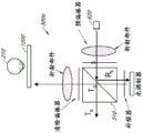
Fig. 10A and 10B show schematic plan views of a Polarizing Beam Splitter (PBS) display assembly including a polarizing beam splitter, a light source, and a light modulator.
FIG. 11 shows a schematic plan view of a bi-fold (twin-fold) PBS display assembly including a polarizing beam splitter, a light source, a light modulator, and a reflector.
Fig. 12 shows a schematic plan view of a bi-fold PBS display assembly with light leakage.
Fig. 13A-13B show schematic plan views of PBS display assemblies with light leakage that does not reach the viewer.
Fig. 14A-14B show schematic cross-sectional views of a PBS display assembly with light leakage to the viewer.
Fig. 14C shows a light intensity map (map) showing the effect of light leakage on an image.
Fig. 15 shows a PBS display assembly with two spaced polarizers.
Fig. 16 shows a PBS display assembly with two spaced apart polarizers with an interposed (intervening) anti-reflection polarizer.
FIG. 17 illustrates a plate type beam splitter having two spaced polarizers on opposite surfaces of an optically transmissive spacer.
FIG. 18 shows a curved plate type beam splitter with two spaced polarizers on opposite surfaces of an optically transmissive spacer.
FIG. 19 shows a plate type beam splitter incorporating an interposed anti-reflective polarizer.
The drawings are provided to illustrate example embodiments, not to limit the scope of the disclosure, and are not necessarily drawn to scale. Like reference numerals refer to like features throughout.
Detailed Description
In some display devices, a polarizing beam splitter may be used to direct light from a light source to a light modulator, which may then modulate the light through the polarizing beam splitter and reflect it back to a viewer. It should be understood that the modulation of light by the light modulator may be said to encode the light with image information and then propagate the light to the viewer. Fig. 10A and 10B show schematic plan views of Polarizing Beam Splitter (PBS) display assemblies 500A and 500B that have been developed to provide image information to a viewer via a waveguide assembly 1200. Display assemblies 500a and 500b include a Polarizing Beam Splitter (PBS)510, a light source (e.g., a light emitting diode or LED), and a light modulator. As shown, a pre-polarizer may be provided between the PBS 510 and the light source. The pre-polarizer may be configured to selectively transmit s-polarized light to the PBS 510, the PBS 510 then reflecting the s-polarized light to a light modulator, e.g., a spatial light modulator, that both modulates the light to form an image and reflects the modulated light through the PBS 510 to incoupling optical elements of the waveguide assembly 1200, which waveguide assembly 1200 delivers the light to the viewer's eye 210. It should be understood that the light modulator converts the received s-polarized light to p-polarized light, and the PBS510 selectively reflect s-polarized light (R)s) And transmits p-polarized light (T)p). A clean-up polarizer may be provided between the PBS 510 and the waveguide assembly 1200 to remove unintentionally transmitted light.
Fig. 10B shows an alternative arrangement in which a pre-polarizer transmits p-polarized light to the PBS 510. The p-polarized light travels through the PBS 510, is reflected by the light modulator and modulated back into the PBS 510 as s-polarized light. PBS 510 then reflects the s-polarized light toward waveguide assembly 1200.
As a convention herein with reference to the light rays shown in the figures, the letters s and p denote light having a unique polarization (e.g., light having an s-polarization state and light having a p-polarization state, respectively), and the letters T and R denote transmitted light and reflected light, respectively. Thus, TpRepresenting transmitted light having p polarization state, RsRepresenting light having an s-polarization state.
It should be appreciated that the light source may need to be spaced a distance from the PBS 510 due to optical limitations. This may undesirably increase the volume occupied by the PBS display assemblies 500a, 500b, where the distance is long.
More compact PBS display assemblies are provided herein. Fig. 11 shows a schematic plan view of a bi-fold PBS display assembly 600 that includes a polarizing beam splitter 610, a light source 620, a light modulator, and a reflector or reflective optic (optical). In some embodiments, the light source 620 is a Light Emitting Diode (LED). In some other embodiments, the light source 620 may be, but is not limited to, a fluorescent lamp or an incandescent lamp. As shown, a pre-polarizer may be provided between the light source and the PBS 610. The pre-polarizer transmits light having one polarization (e.g., S-polarized light, S) to the PBS 610, and the PBS 610 then transmits the S-polarized light (R)s) To the reflective optical component. The reflective optics reflect light through the PBS 610 to a light modulator, e.g., a spatial light modulator. Preferably, the light modulator is a spatial light modulator that modulates incident light to form an image and also reflects and changes the polarization of the incident light. In some embodiments, the light modulator is a reflective liquid crystal display, such as a Liquid Crystal On Silicon (LCOS) display. The modulated and reflected light from the light modulator is reflected back to the PBS 610, and the PBS 610 reflects the light toward the waveguide setPiece 1200.
With continued reference to fig. 11, in some embodiments, a Quarter Wave Plate (QWP) may be disposed between the PBS 610 and the reflective optic. Additionally, in some embodiments, a compensator may be disposed between the light modulator and the PBS 610. In some embodiments, a clean-up polarizer may be provided between the PBS 610 and the waveguide assembly 1200 to remove unintentionally transmitted light. In some embodiments, refractive optical components (e.g., one or more lens structures) may be disposed between the clean-up polarizer and the waveguide assembly 1200. For example, a clean-up polarizer may be located on the light output face of PBS 610 facing the clean-up polarizer, or may be spaced apart from PBS 610 in the light path between PBS 610 and waveguide assembly 1200.
Advantageously, the use of catadioptric optics in combination with PBS 610, light source 620 and light modulator provides a compact PBS display assembly 600 by reducing the required spacing between light source 620 and PBS 610 relative to configurations without catadioptric optics, such as those shown in figures 10A and 10B. PBS display assembly 600 may also be referred to as a bi-fold assembly due to multiple reflections of light in the assembly. Advantageously, the multiple reflections provide a long path length for light to the light modulator in a more compact package relative to the display assemblies 500A and 500B of fig. 10A and 10B.
It should be understood, however, that a PBS may not be completely selective in reflecting and/or transmitting light of a particular polarization. For example, rather than reflecting all s-polarized light from the light source 620 to the catadioptric optical component, some of that light may be transmitted through the PBS 610 directly toward the viewer (via the waveguide assembly 1200), causing glare that may reduce contrast. Fig. 12 shows a schematic plan view of a bi-fold PBS display assembly 600 with light leakage. As shown, s-polarized light from light source 620 is taken as TsTo the PBS 610. Most of the s-polarized light from the light source 620 is reflected by the PBS 610 to the reflective optics, however, a small portion may be transmitted through the PBS 610 directly toward the waveguide assembly 1200. This directly transmitted light is not modulated by the light modulator and may result in a reduced perception of image quality and glare.
It has been found that there is no such glare and degradation of image quality in larger PBS display assemblies that do not use reflective optics. For example, fig. 13A-13B show schematic plan views of PBS display assemblies 500a and 500B with light leakage that does not reach the viewer's eye 210. However, due to the orientation of the viewer's eye 210 relative to the light source 620, light unintentionally transmitted by the PBS 610 propagates in a direction other than toward the waveguide assembly 1200.
14A-14B illustrate schematic cross-sectional views of PBS display assembly 600 with light leakage that does not reach the viewer via waveguide assembly 1200. Fig. 14A shows how the leaked light is focused and fig. 14B shows how the light used to generate the image is focused. Notably, the leaked light forms two distinct hot spots that can be seen by a viewer. Fig. 14C shows a map of light intensity showing the effect of light leakage on an image. As shown, hot spots 900 caused by light leakage are apparent.
Advantageously, in some embodiments, a PBS having two spaced polarizers may be used to mitigate light leakage. Fig. 15 shows a PBS display assembly 700 having two spaced apart polarizers 710a and 710b separated by a gap 720. Fig. 15 shows the PBS 710 of the isolated display assembly 700. Polarizers 710a and 710b separate the PBS 710 into two portions 730a and 730 b. The components of PBS display assembly 700 may be similar to the components of PBS display assembly 600 (fig. 11), except that PBS 610 is replaced with PBS 710. In some embodiments, PBS display assembly 700 may be similar to PBS display assembly 600 and have some or all of the components discussed and illustrated in fig. 11, except that PBS 710 replaces PBS 610 in PBS display assembly 600. PBS 710 itself may be similar or identical to PBS 610, except for the presence of polarizers 710a and 710b and intervening gap 720.
With continued reference to fig. 15, in some embodiments, the PBS 710 may have the overall shape of a rectangular solid, e.g., a cube. The solid body may be divided into two parts along a line extending diagonally on two opposite sides of the solid body. In some embodiments, PBS 710 may be formed from two triangular sections or prisms 730a and 730b that together form a rectangular solid, e.g., a cube. The two triangular portions or prisms 730a and 730b may be joined together by an adhesive (e.g., an index-matched adhesive). Triangular portions 730a and 730b may be formed from an optically transmissive material, such as one or more of glass and plastic. Similarly, the adhesive may be optically transmissive.
In some embodiments, the polarizers 710a and 710b may be wire grid polarizers, which are formed, for example, by a pattern of parallel wires (such as metal wires). In other embodiments, the polarizers 710a and 710b can be thin film PBS coatings (e.g., dichroic (e.g., MacNeille PBS.) in some other embodiments, the polarizers 710a and 710b can be multilayer birefringent stacks.
With continued reference to fig. 15, gap 720 may be filled with an index-matching material, e.g., a material having an index of refraction matching the index of refraction of portions 730a and 730 b. For example, the refractive index of the material in gap 720 may differ from the refractive indices of portions 730a and 730b by about 0.1 or less, about 0.05 or less, about 0.03 or less, or about 0.02 or less. In some embodiments, the index-matching material is an index-matching adhesive that bonds portions 730a and 730b together. In some embodiments, the width of the gap is about 10nm or greater, 50nm or greater, 100 nanometers or greater, 200nm or greater, 500nm or greater, 1 μm or greater, 5 μm or greater, or 10 μm or greater. Further, in some embodiments, the width is 20 μm or less, or 15 μm or less. It is to be understood that the material filling the gap 720 may form an optically transmissive spacer 722.
Advantageously, the opposing polarizers 710a and 710b may reduce light leakage and significantly increase contrast. For example, in some embodiments, the amount of light leaked may be 1.7% without polarizers 710a and 710b, which corresponds to a contrast ratio of 60: 1. In the presence of polarizers 710a and 710b, the contrast can theoretically be increased to 3600:1 by the square of the molecules. In some embodiments, the actual contrast may be 500:1 or higher, 1000:1 or higher, or 2000:1 or higher. Advantageously, when the polarizers 710a and 710b are used, hot spots caused by the transmission of leaked light are not visually discernable.
With continued reference to FIG. 15, a spacer 722 filling the gap 720 between the polarizers 710a and 710b may be used as a waveguide. For example, light may propagate within the spacers 722 due to reflection (e.g., total internal reflection) at the mutually facing opposing surfaces of the polarizers 710a and 710 b. Such reflections may be undesirable and may lead to image artifacts.
In some embodiments, an absorbing polarizer may be disposed within spacer 722 between polarizers 710a and 710 b. Fig. 16 shows a PBS display assembly 700 having two spaced-apart polarizers 710a and 710b with an interposed anti-reflection polarizer 740 for both spaced-apart polarizers 710a and 710 b. The anti-reflective polarizer 740 may be configured to absorb light in the gap between the polarizers 710a and 710b, thereby preventing or reducing reflection between the polarizers 710a and 710 b. The polarization of the anti-reflective polarizer may be selected to preferentially absorb polarized light transmitted by polarizer 710a, which polarizer 710a receives light from a light source in the first example. For example, anti-reflective polarizer 740 may preferentially absorb Ts。TsIs the primary function of the polarizer 740. The anti-reflective polarizer 740 may extend fully or only partially along the length of the gap 720. In some embodiments, anti-reflective polarizer 740 is an absorptive polarizer. In some other embodiments, the anti-reflective polarizer 740 is an e-mode polarizer, an o-mode polarizer, or a polarization stack with color selectivity. In some embodiments, the anti-reflection polarizer 740 may be a combination of the polarizers and/or polarization stacks described above. Advantageously, the use of anti-reflection polarizer 740 in conjunction with polarizers 710a and 710b may provide a contrast ratio of 2000:1 or greater.
With continued reference to FIG. 16, the anti-reflective polarizer 740 is separated from the spaced apart polarizers 710a and 710b by gaps 720a and 720 b. In some embodiments, gaps 720a and 720b each have a width of about 10nm or greater, 50nm or greater, 100nm or greater, 200nm or greater, 500nm or greater, 1 μm or greater, 5 μm or greater, or 10 μm or greater. Additionally, in some embodiments, the width of each gap 720a and 720b is 20 μm or less. In other words, anti-reflective polarizer 740 is disposed within spacer 722 and separates spacer 722 into portions 722a and 722 b. Portion 722a has a thickness 720a and portion 722b has a thickness 720 b.
It will be appreciated that in some embodiments, the spacers 722 may themselves be substrates supporting the spaced polarizers. In such embodiments, the spacers are preferably in the form of plates of sufficient rigidity and mechanical stability to support the spaced apart polarizers on either side of the spacer rather than prisms. FIG. 17 shows a plate type beam splitter 810 having two spaced polarizers 710a and 710b on opposite surfaces or faces 820a and 820b of an optically transmissive spacer 820. The optically transmissive spacer 820 may be formed of, for example, glass or an optically transmissive polymer. It should be understood that in some embodiments, beam splitter 810 may replace beam splitter 610 of display assembly 600.
The spaced polarizers 710a and 710b may be as described herein. As described above, in some embodiments, the polarizers 710a and 710b can be wire grid polarizers formed from a pattern of, for example, parallel wires (such as metal wires). In some embodiments, polarizers 710a and 710b may be thin film PBS coatings (e.g., dichroic coatings such as MacNeille PBS). In some other embodiments, the polarizers 710a and 710b may be multilayer birefringent stacks. The polarizers 710a and 710b may be the same type of polarizer (e.g., both polarizers 710a and 710b may be wire grid polarizers). In some other embodiments, the polarizers 710a and 710b may be different types of polarizers (e.g., one may be a wire grid polarizer and the other may be a thin film PBS coating).
With continued reference to fig. 17, in some embodiments, the spacer 820 may have the shape of a rectangular plate and the plate may be flat. The opposing faces 820a and 820b may each be planar and may be substantially parallel to each other, which in turn may cause the polarizers 710a and 710b to be substantially parallel to each other.
In some other embodiments, the spacer 820 may have a curved plate shape. FIG. 18 shows a curved plate type beam splitter 810 having two spaced polarizers 710a and 710b on opposite surfaces 820a and 820b of a spacer 820. As shown, the spacer 820 may be curved along a length dimension of the spacer 820. In some embodiments, the opposing surfaces 820a and 820b are substantially parallel to each other as are the polarizers 710a and 710 b. It should be appreciated that in some embodiments, the spacer 820 may be curved to provide curvature to the polarizers 710a and 710b, which may then advantageously provide a degree of beam shaping to the light reflected by the polarizers 710a and 710 b.
As discussed herein, in some cases, the spacer 820 may undesirably act as a waveguide, where light is reflected back and forth between the surfaces 820a and 820 b. To reduce such reflections, in some embodiments, an anti-reflective polarizer may be provided within spacer 820. FIG. 19 shows a plate type beam splitter 810 including an interposed anti-reflective polarizer 740. The anti-reflective polarizer 740 may be as described herein. For example, in some embodiments, the anti-reflective polarizer 740 may be an absorptive polarizer. In some other embodiments, the anti-reflective polarizer 740 may be an e-mode polarizer, an o-mode polarizer, or a polarization stack with color selectivity, as disclosed herein. In some embodiments, the anti-reflection polarizer 740 may be a combination of the polarizers and/or polarization stacks described above.
With continued reference to FIG. 19, the anti-reflection polarizer 740 may extend fully or only partially along the length of the plate type beam splitter 810. In some embodiments, anti-reflective polarizer 740 may divide spacer 820 into two portions 820a and 820 b. The portions may be joined together by, for example, an optically transmissive adhesive, such as an index-matching adhesive. It should be understood that although shown as a flat plate for ease of illustration, the spacers 820 may also be curved as described above with reference to fig. 18. In such embodiments, the anti-reflective polarizer 740 may follow the curve of the spacer 820.
Example display System
It should be understood that the PBS assembly can be used in a variety of lighting applications requiring a low-volume assembly. For example, the PBS assembly may be advantageously used in portable, e.g., head-mounted, display systems.
In some embodiments, the PBS assembly may be used for image generation in an augmented or virtual reality display system. In some embodiments, these display systems may be wearable and portable, and may present images on multiple depth planes.
Referring to fig. 1, an augmented reality scene 1 is depicted. It will be appreciated that modern computing and display technology has facilitated the development of systems for so-called "virtual reality" or "augmented reality" experiences, in which digitally reproduced images or portions thereof are presented to a user in a manner in which they appear to be, or may be perceived as, real. Virtual reality (or "VR") scenes typically involve the presentation of digital or virtual image information, while being opaque to other real-world visual inputs; augmented reality (or "AR") scenes typically involve the presentation of digital or virtual image information as an enhancement to the visualization of the real world around the user. A mixed reality (or "MR") scene is an AR scene and typically involves virtual objects that are integrated into and responsive to the natural world. For example, an MR scene may include AR image content that appears to be blocked by or perceived as interacting with objects in the real world.
With continued reference to fig. 1, an augmented reality scene 1 is shown. A user of AR technology sees a real world park-like setting 1100 featuring people, trees, buildings in the background, and a concrete platform 1120. In addition to these items, the user of AR technology also perceives that he "sees" a robotic statue 1110 standing on a real world platform 1120, as well as a flying cartoon-style avatar character 1130, which appears to be an avatar of bumblebee, even though these elements 1130, 1110 do not exist in the real world. As the human visual perception system is complex and it is challenging to produce a comfortable, natural, rich presentation of virtual image elements that facilitates along with other virtual or real-world image elements.
Fig. 2 shows an example of a wearable display system 80. Display system 80 includes a display 62, and various mechanical and electronic modules and systems that support the functionality of display 62. The display 62 may be coupled with a frame 64 that may be worn by a display system user or viewer 60 and configured to position the display 62 in front of the eyes of the user 60. In some embodiments, the display 62 may be considered to be eyeglasses (eyewear). In some embodiments, a speaker 66 is coupled to the frame 64 and is located near the ear canal of the user 60 (in some embodiments, another speaker (not shown) is located near another ear canal of the user to provide stereo/shapeable sound control). In some embodiments, the display system may also include one or more microphones 67 or other devices to detect sound. In some embodiments, the microphone is configured to allow a user to provide inputs or commands to the system 80 (e.g., selection of voice menu commands, natural language questions, etc.) and/or may allow audio communication with others (e.g., users with other similar display systems).
With continued reference to fig. 2, the display 62 is operatively coupled 68 (such as by a wired lead or wireless connection) to a local data processing and module 70, which local data processing and module 70 may be mounted in a variety of configurations, such as fixedly attached to the frame 64, fixedly attached to a helmet or hat worn by the user, embedded within a headset, or otherwise removably attached to the user (e.g., in a backpack configuration, in a band-coupled configuration). The local processing and data module 70 may include a hardware processor and digital memory such as non-volatile memory (e.g., flash memory or a hard drive), both of which may be used to assist in processing, caching, and storing data. The data includes: a) data captured from sensors (which may be operatively coupled to the frame 64 or otherwise operatively attached to the user 60, for example, image capture devices such as cameras, microphones, inertial measurement units, accelerometers, compasses, GPS units, radios, and/or gyroscopes; and/or b) data acquired and/or processed using remote processing module 72 and/or remote data repository 74, which may be transmitted to display 62 after such processing or retrieval. Local processing and data module 70 may be operatively coupled to remote processing module 72 and remote data repository 74 by communication links 76, 78, such as via wired or wireless communication links, so that these remote modules 72, 74 are operatively coupled to each other and may serve as resources for local processing and data module 70. In some embodiments, the local processing and data module 70 may include one or more of an image capture device, a microphone, an inertial measurement unit, an accelerometer, a compass, a GPS unit, a radio, and/or a gyroscope. In some other embodiments, one or more of these sensors may be attached to the frame 64 or may be a separate structure that communicates with the local processing and data module 70 through a wired or wireless communication path.
With continued reference to fig. 2, in some embodiments, the remote processing module 72 may include one or more processors configured to analyze and process data and/or image information. In some embodiments, the remote data repository 74 may include a digital data storage facility that may be available through the internet or other network configuration in a "cloud" resource configuration. In some embodiments, the remote data repository 74 may include one or more remote servers that provide information, e.g., information for generating augmented reality content, to the local processing and data module 70 and/or the remote processing module 72. In some embodiments, all data is stored and all calculations are performed in the local processing and data module, allowing for fully autonomous use from the remote module.
Referring now to fig. 3, the perception of an image as "three-dimensional" or "3-D" may be achieved by providing a slightly different presentation of the image to each eye of the viewer. Fig. 3 illustrates a conventional display system for simulating a three-dimensional image for a user. Two different images 5, 7-one for each eye 4, 6-are output to the user. The images 5, 7 are spaced from the eyes 4, 6 by a distance 10 along an optical or z-axis parallel to the viewer's line of sight. The images 5, 7 are flat and the eyes 4, 6 can focus on the images by assuming a single accommodation (accmod) state. Such systems rely on the human visual system to combine the images 5, 7 to provide a depth perception and/or scale (scale) of the combined image.
However, it should be appreciated that the human visual system is more complex and more challenging to provide a true perception of depth. For example, many viewers of conventional "3-D" display systems find such systems uncomfortable or unable to perceive a sense of depth at all. Without being limited by theory, it is believed that a viewer of an object may perceive the object as "three-dimensional" due to a combination of vergence and accommodation. Vergence movement of the two eyes relative to each other (i.e., the rotational action of the pupils to gaze at an object toward or away from each other to converge the eye's line of sight) is closely related to the focusing (or "accommodation") of the lenses and pupils of the eyes. Under normal circumstances, changing the focus of the lens of the eye or adapting the eye to change focus when switching from one object to another located at a different distance will automatically result in a matching change that causes convergence to the same distance under a relationship known as "accommodation-vergence reflex" and pupil dilation or constriction. Also, under normal circumstances, a change in vergence will cause a change in the fit of the lens shape and pupil size accommodation. As described herein, many stereoscopic or "3-D" display systems display a scene to each eye using slightly different presentations (and thus slightly different images) so that the human visual system perceives a three-dimensional perspective. However, such systems are uncomfortable for many viewers, because among other things, such systems simply provide different presentations of a scene, and the eye views all image information in a single state of accommodation, and works against the "accommodation-vergence reflection". A display system that provides a better match between accommodation and vergence may result in a more realistic and comfortable three-dimensional image simulation.
FIG. 4 illustrates aspects of a method of simulating a three-dimensional image using multiple depth planes. With continued reference to fig. 4, objects at different distances from the eyes 4, 6 on the z-axis are accommodated by the eyes 4, 6 such that those objects are in focus (in focus). The eyes (4 and 6) assume a particular adaptation state to bring objects at different distances along the z-axis into focus. Thus, it can be said that a particular accommodation state is associated with a particular one of the depth planes 14, which has an associated focal length, such that an object or part of an object in a particular depth plane is in focus when the eye is in the accommodation state of that depth plane. In some embodiments, the three-dimensional image may be simulated by providing a different presentation of the image for each of the eyes 4, 6, and may also be simulated by providing a different presentation of the image corresponding to each of the depth planes. Although shown as separate for clarity of illustration, it is understood that the fields of view of the eyes 4, 6 may overlap, for example, as the distance along the z-axis increases. Additionally, while shown as flat for ease of illustration, it is understood that the profile of the depth plane may be curved in physical space such that all features in the depth plane are in focus with the eye under certain accommodation conditions.
The distance between the object and the eye 4 or 6 may also change the amount of divergence of the light from the object as seen by the eye. Fig. 5A-5C illustrate the relationship between distance and ray divergence. The distance between the subject and the eye 4 is represented by the order of decreasing distance R1, R2, and R3. As shown in fig. 5A-5C, the light rays become more divergent as the distance to the object decreases. As the distance increases, the light rays become more collimated. In other words, it can be said that the light field generated by a point (object or part of an object) has a spherical wavefront curvature that is a function of how far the point is from the user's eye. As the distance between the object and the eye 4 decreases, the curvature increases. Thus, at different depth planes, the divergence of the light rays is also different, the divergence increasing as the distance between the depth plane and the viewer's eye 4 decreases. Although only a single eye 4 is shown in fig. 5A-5C and other figures herein for clarity of illustration, it should be understood that the discussion regarding eyes 4 may apply to both eyes 4 and 6 of the viewer.
Without being limited by theory, it is believed that the human eye can generally interpret a limited number of depth planes to provide depth perception. Thus, by providing the eye with different presentations of the image corresponding to each of these limited number of depth planes, a highly reliable simulation of perceived depth may be achieved. The different presentations may be individually focused by the eyes of the viewer, thereby facilitating providing depth cues to the user based on accommodation of the eyes required to focus on different image features of a scene located on different depth planes, and/or based on viewing different image features located on different depth planes out of focus.
Fig. 6 shows an example of a waveguide stack for outputting image information to a user. The display system 1000 includes a waveguide stack or stacked waveguide assembly 178 that may be used to provide three-dimensional perception to the eye/brain using a plurality of waveguides 182, 184, 186, 188, 190. In some embodiments, the display system 1000 is the system 80 of fig. 2, where fig. 6 schematically illustrates some portions of the system 80 in more detail. For example, the waveguide assembly 178 may be part of the display 62 of FIG. 2. It should be understood that in some embodiments, the display system 250 may be considered a light field display.
With continued reference to fig. 6, the waveguide assembly 178 may further include a plurality of features 198, 196, 194, 192 located between the waveguides. In some embodiments, the features 198, 196, 194, 192 may be one or more lenses. The waveguides 182, 184, 186, 188, 190 and/or the plurality of lenses 198, 196, 194, 192 may be configured to transmit image information to the eye at various levels of wavefront curvature or ray divergence. Each waveguide level may be associated with a particular depth plane and may be configured to output image information corresponding to that depth plane. The image injection devices 200, 202, 204, 206, 208 may serve as light sources for the waveguides and may be used to inject image information into the waveguides 182, 184, 186, 188, 190, each of which may be configured to distribute incident light through each respective waveguide for output to the eye 4, as described herein. Light exits the output surfaces 300, 302, 304, 306, 308 of the image injection devices 200, 202, 204, 206, 208 and is injected into the respective input surfaces 382, 384, 386, 388, 390 of the waveguides 182, 184, 186, 188, 190. In some embodiments, each of the input surfaces 382, 384, 386, 388, 390 may be an edge of a respective waveguide, or may be a portion of a major surface of the respective waveguide (i.e., one of the waveguide surfaces that directly faces the world 144 or the viewer's eye 4, in some embodiments, a single beam of light (e.g., a collimated beam) may be injected into each waveguide to output the entire field of view of the collimated beam of light directed toward the eye 4 at a particular angle (and amount of divergence) corresponding to the depth plane associated with the particular waveguide, hi some embodiments, a single one of the image injection devices 200, 202, 204, 206, 208 may be associated with multiple (e.g., three) of the waveguides 182, 184, 186, 188, 190 and inject light into multiple (e.g., three) of the waveguides 182, 184, 186, 188, 190.
In some embodiments, the image injection devices 200, 202, 204, 206, 208 are discrete displays, each display producing image information for injection into a respective waveguide 182, 184, 186, 188, 190, respectively. In some other embodiments, the image injection devices 200, 202, 204, 206, 208 are outputs of a single multiplexed display that can duct image information to each of the image injection devices 200, 202, 204, 206, 208, e.g., via one or more light pipes (such as fiber optic cables). It is to be appreciated that the image information provided by the image injection devices 200, 202, 204, 206, 208 can include light of different wavelengths or colors (e.g., different component colors, as discussed herein).
In some embodiments, the light injected into the waveguides 182, 184, 186, 188, 190 is provided by a PBS display assembly 209 that includes a light output module 209a, which may include a light source, such as a Light Emitting Diode (LED) or a fluorescent bulb. It should be understood that PBS display assembly 209 may correspond to PBS display assemblies 600 (fig. 12) and 700 (fig. 15 and 16), with light output module 209a corresponding to light source 620 and light modulator 209c corresponding to the light modulators of PBS display assemblies 600 (fig. 12) and 700 (fig. 15 and 16). Light from the light output module 209a can be directed to a light modulator 209c and modified by the light modulator 209c (e.g., a spatial light modulator) via the PBS 209 b. The light modulator 209c may be configured to vary the perceived intensity of light injected into the waveguides 182, 184, 186, 188, 190. Examples of spatial light modulators include Liquid Crystal Displays (LCDs), which include Liquid Crystal On Silicon (LCOS) displays. It should be understood that the image injection devices 360, 370, 380, 390, 400 are schematically shown and, in some embodiments, may represent different optical paths and locations in a common projection system configured to output light into one of the associated waveguides 270, 280, 290, 300, 310.
The controller 210 controls the operation of one or more of the stacked waveguide assemblies 178, including the operation of the image injection devices 200, 202, 204, 206, 208, the light source 209a, and the light modulator 209 b. In some embodiments, the controller 210 is part of the local data processing module 70. The controller 210 includes programming (e.g., instructions in a non-transitory medium) that adjusts the timing and provision of image information to the waveguides 182, 184, 186, 188, 190, for example, according to any of the various aspects disclosed herein. In some embodiments, the controller may be a single unitary device or a distributed system connected by wired or wireless communication channels. In some embodiments, the controller 210 may be part of the processing module 70 or 72 (FIG. 1).
With continued reference to fig. 6, the waveguides 182, 184, 186, 188, 190 may be configured to propagate light within each respective waveguide by Total Internal Reflection (TIR). The waveguides 182, 184, 186, 188, 190 may each be planar or have other shapes (e.g., curved) with top and bottom major surfaces and edges extending between the top and bottom major surfaces. In the illustrated configuration, the waveguides 182, 184, 186, 188, 190 may each include out coupling (outcoupling) optical elements 282, 284, 286, 288, 290 configured to extract light out of the waveguides by redirecting light propagating within each respective waveguide out of the waveguide to output image information to the eye 4. The extracted light may also be referred to as outcoupled light, and the outcoupled optical element light may also be referred to as light extraction optical elements. The extracted light beam is output by the waveguide at a position where the light propagating in the waveguide is irradiated to the light extraction optical element. The outcoupling optical elements 282, 284, 286, 288, 290 may, for example, comprise gratings of diffractive optical characteristics, as discussed further herein. Although illustrated as being disposed at the bottom major surface of the waveguides 182, 184, 186, 188, 190 for ease of description and clarity of drawing, in some embodiments the out-coupling optical elements 282, 284, 286, 288, 290 may be disposed at the top and/or bottom major surfaces and/or may be disposed directly in the volume of the waveguides 182, 184, 186, 188, 190, as discussed further herein. In some embodiments, the out-coupling optical elements 282, 284, 286, 288, 290 may be formed in a layer of material attached to a transparent substrate to form the waveguides 182, 184, 186, 188, 190. In some other embodiments, the waveguides 182, 184, 186, 188, 190 may be a single piece of material, and the out-coupling optical elements 282, 284, 286, 288, 290 may be formed on a surface of the piece of material and/or in an interior of the piece of material.
With continued reference to fig. 6, as discussed herein, each waveguide 182, 184, 186, 188, 190 is configured to output light to form an image corresponding to a particular depth plane. For example, the waveguide 182 closest to the eye may be configured to deliver collimated light, as injected into such a waveguide 182, to the eye 4. The collimated light may represent an optically infinite focal plane. The next up waveguide 184 may be configured to send out collimated light that passes through a first lens 192 (e.g., a negative lens) before it can reach the eye 4; such a first lens 192 may be configured to produce a slightly convex wavefront curvature such that the eye/brain interprets light from the next upstream waveguide 184 as coming from a first focal plane that is closer inward from optical infinity toward the eye 4. Similarly, the third uplink waveguide 186 has its output light pass through first and second lenses 192, 194 before reaching the eye 4; the combined optical power of the first lens 192 and the second lens 194 may be configured to produce another incremental wavefront curvature such that the eye/brain interprets light from the third waveguide 186 as coming from a second focal plane that faces inward toward the person from optical infinity than light from the next upward traveling waveguide 184.
The other waveguide layers 188, 190 and lenses 196, 198 are similarly configured, with the highest waveguide 190 in the stack sending its output through all lenses between it and the eye for representing the aggregate focal power closest to the human focal plane. To compensate for the stack of lenses 198, 196, 194, 192 when viewing/interpreting light from the world 144 on the other side of the stacked waveguide assembly 178, a compensation lens layer 180 may be disposed at the top of the stack to compensate for the aggregate power of the underlying lens stack 198, 196, 194, 192. This configuration provides as many sensing focal planes as there are waveguide/lens pairs available. The focusing aspects of the out-coupling optical elements and lenses of the waveguide may be static (i.e., not dynamic or electro-active). In some alternative embodiments, either or both may be dynamic using electroactive characteristics.
In some embodiments, two or more of the waveguides 182, 184, 186, 188, 190 may have the same associated depth plane. For example, multiple waveguides 182, 184, 186, 188, 190 may be configured to output images set to the same depth plane, or multiple subsets of waveguides 182, 184, 186, 188, 190 may be configured to output images set to the same multiple depth planes, one set for each depth plane. This may provide advantages for forming tiled images to provide an extended field of view at those depth planes.
With continued reference to fig. 6, the out-coupling optical elements 282, 284, 286, 288, 290 may be configured to redirect light out of their respective waveguides and output that light with an appropriate amount of divergence or collimation for the particular depth plane associated with that waveguide. As a result, waveguides having different associated depth planes may have different configurations of out-coupling optical elements 282, 284, 286, 288, 290 that output light having different amounts of divergence depending on the associated depth plane. In some embodiments, the light extraction optics 282, 284, 286, 288, 290 may be volume or surface features that may be configured to output light at a particular angle. For example, the light extraction optical elements 282, 284, 286, 288, 290 may be volume holograms, surface holograms, and/or diffraction gratings. In some embodiments, the features 198, 196, 194, 192 may not be lenses; rather, they may simply be spacers (e.g., cladding layers and/or structures for forming air gaps).
In some embodiments, the outcoupling optical elements 282, 284, 286, 288, 290 are diffractive features that form a diffraction pattern, or "diffractive optical elements" (also referred to herein as "DOEs"). Preferably, the DOE has a sufficiently low diffraction efficiency such that only a portion of the light of the beam is deflected towards the eye 4 by each intersection of the DOE, while the remainder continues to move through the waveguide via total internal reflection. The light carrying the image information is thus split into a plurality of related exit beams which exit the waveguide at a plurality of locations and as a result are exit emissions in a fairly uniform pattern towards the eye 4 for this particular collimated beam bouncing within the waveguide.
In some embodiments, one or more DOEs may be switchable between an "on" state in which they are actively diffracting and an "off" state in which they are not significantly diffracting. For example, a switchable DOE may comprise a polymer dispersed liquid crystal layer, wherein the droplets comprise a diffraction pattern in the host medium, and the refractive index of the droplets may be switched to substantially match the refractive index of the host material (in which case the pattern DOEs not significantly diffract incident light), or the droplets may be switched to a refractive index that DOEs not match the refractive index of the host medium (in which case the pattern actively diffracts incident light).
Fig. 7 shows an example of an outgoing light beam output by a waveguide. One waveguide is shown, but it is understood that other waveguides in waveguide assembly 178 may function similarly, where waveguide assembly 178 includes a plurality of waveguides. Light 400 is injected into the waveguide 182 at the input surface 382 of the waveguide 182 and propagates within the waveguide 182 by TIR. At the point where the light 400 is incident (imagey) on the DOE 282, a portion of the light exits the waveguide as an exit beam 402. The exit beam 402 is shown as being substantially parallel, but as discussed herein, depending on the depth plane associated with the waveguide 182, the exit beam 402 may also be redirected at an angle (e.g., to form a diverging exit beam) to propagate to the eye 4. It will be appreciated that the substantially parallel outgoing light beams may be indicative of a waveguide having outcoupling optical elements that will couple out light to form an image that appears to be disposed on a depth plane at a large distance (e.g., optical infinity) from the eye 4. Other waveguides or other sets of outcoupling optical elements may output a more divergent exit beam pattern, which would require the eye 4 to adapt to a closer distance to focus it on the retina and would be interpreted by the brain as light from a distance closer to the eye 4 than optical infinity.
In some embodiments, a full color image may be formed at each depth plane by superimposing images of each component color (e.g., three or more component colors). Fig. 9 illustrates an example of a stacked waveguide assembly, wherein each depth plane includes images formed using a plurality of different component colors. The illustrated embodiment shows depth planes 14a-14f, but more or less depths are contemplated. Each depth plane may have three component color images associated with it: a first image G of a first color; a second image R of a second color; and a third image B of a third color. For the diopters behind letters G, R and B, different depth planes are indicated by different numbers in the figure. As an example, the number following each of these letters represents diopter (1/m), or the inverse distance of the depth plane from the viewer, and each box in the figure represents a separate component color image. In some embodiments, to account for differences in the focus of the eye on light of different wavelengths, the precise placement of the depth planes for the different component colors may be varied. For example, different component color images for a given depth plane may be placed on the depth plane corresponding to different distances from the user. Such an arrangement may increase visual acuity and user comfort and/or may reduce chromatic aberrations.
In some embodiments, each component color of light may be output by a single dedicated waveguide, and thus, each depth plane may have multiple waveguides associated therewith. In such embodiments, each box in the figure including the letter G, R or B may be understood to represent a separate waveguide, and each depth plane may provide three waveguides, with each depth plane providing three component color images. Although the waveguides associated with each depth plane are shown adjacent to each other in this figure for ease of description, it should be understood that in a physical device, the waveguides may all be arranged in a stack with one waveguide per layer. In some other embodiments, multiple component colors may be output by the same waveguide, such that, for example, each depth plane may provide only a single waveguide.
With continued reference to fig. 8, in some embodiments, G is green, R is red, and B is blue. In some other embodiments, other colors (including magenta and cyan) associated with other wavelengths of light may be used in addition to or in place of one or more of red, green or blue.
It should be understood that throughout this disclosure reference to light of a given color will be understood to include light of one or more wavelengths within a range of wavelengths that a viewer perceives as having light of that given color. For example, red light may include light at one or more wavelengths in the range of about 620-780nm, green light may include light at one or more wavelengths in the range of about 492-577nm, and blue light may include light at one or more wavelengths in the range of about 435-493 nm.
Referring now to fig. 9A, in some embodiments, it may be desirable to redirect light incident on the waveguide to couple the light into the waveguide. Incoupling optical elements may be used to redirect and couple light into their respective waveguides. Fig. 9A illustrates a cross-sectional side view of an example of a plurality or set of stacked waveguides 1200, each including an incoupling optical element. Each waveguide may be configured to output light of one or more different wavelengths, or one or more different wavelength ranges. It should be understood that the stack 1200 may correspond to the stack 178 (fig. 6), and that the waveguides 1200 of the out-of-stack may correspond to a portion of the plurality of waveguides 182, 184, 186, 188, 190, except that one or more of the light from the image injection devices 200, 202, 204, 206, 208 is injected into the waveguides from a location where it is desired that the light be redirected for in-coupling.
The illustrated stacked waveguide set 1200 includes waveguides 1210, 1220, and 1230. Each waveguide includes associated incoupling optical elements, such as incoupling optical element 1212 disposed on a major surface (e.g., an upper major surface) of waveguide 1210, incoupling optical element 1224 disposed on a major surface (e.g., an upper major surface) of waveguide 1220, and incoupling optical element 1232 disposed on a major surface (e.g., an upper major surface) of waveguide 1230. In some embodiments, one or more of the incoupling optical elements 1212, 1222, 1232 may be disposed on the bottom major surface of the respective waveguide 1210, 1220, 1230 (particularly where the one or more incoupling optical elements are reflective, deflecting optical elements). As shown, incoupling optical elements 1212, 1222, 1232 may be disposed on the upper major surface of their respective waveguides 1210, 1220, 1230 (or on top of the next lower waveguide), particularly if those incoupling optical elements are transmissive, deflecting optical elements. In some embodiments, the incoupling optical elements 1212, 1222, 1232 may be disposed in the body of the respective waveguides 1210, 1220, 1230. In some embodiments, the incoupling optical elements 1212, 1222, 1232 are wavelength selective, such that they selectively redirect light of one or more wavelengths while transmitting light of other wavelengths, as discussed herein. Although shown on one side or corner of their respective waveguides 1210, 1220, 1230, it should be understood that in some embodiments the incoupling optical elements 1212, 1222, 1232 may be disposed in other regions of their respective waveguides 1210, 1220, 1230.
As shown, the incoupling optical elements 1212, 1222, 1232 may be laterally offset from one another. In some embodiments, each incoupling optical element may be offset such that it receives light without the light passing through another incoupling optical element. For example, each incoupling optical element 1212, 1222, 1232 may be configured to receive light from a different image injection device 1213, 1223, 1233 and may be separated (e.g., laterally spaced) from the other incoupling optical elements 1212, 1222, 1232 such that it does not substantially receive light from the other incoupling optical elements 1212, 1222, 1232.
Each waveguide also includes an associated light distribution element, e.g., light distribution element 1214 disposed on a major surface (e.g., top major surface) of waveguide 1210, light distribution element 1224 disposed on a major surface (e.g., top major surface) of waveguide 1220, and light distribution element 1234 disposed on a major surface (e.g., top major surface) of waveguide 1230. In some other embodiments, light distribution elements 1214, 1224, 1234 may be arranged on the bottom main surface of the associated waveguides 1210, 1220, 1230, respectively. In some other embodiments, light distributing elements 1214, 1224, 1234 may be arranged on top and bottom major surfaces of associated waveguides 1210, 1220, 1230, respectively; or the light distributing elements 1214, 1224, 1234 may be arranged on different ones of the top and bottom main surfaces of different associated waveguides 1210, 1220, 1230, respectively.
The waveguides 1210, 1220, 1230 may be spaced apart and separated by layers of gas and/or solid material. For example, as shown, layer 1218a can separate waveguides 1210 and 1220; and layer 1218b can separate waveguides 1220 and 1230. In some embodiments, layers 1218a and 1218b are formed of a low-index material (i.e., a material having a lower index of refraction than the material forming the immediately adjacent ones of waveguides 1210, 1220, 1230). Preferably, the refractive index of the materials forming layers 1218a, 1218b is less than the refractive index of the materials forming waveguides 1210, 1220, 1230 by 0.05 or more, or 0.10 or less. Advantageously, the low refractive index layers 1218a, 1218b can act as cladding (clad) layers that promote Total Internal Reflection (TIR) of light passing through the waveguides 1210, 1220, 1230 (e.g., between the top and bottom major surfaces of each waveguide). In some embodiments, the layers 1218a, 1218b are formed of air. Although not shown, it is understood that the top and bottom of the illustrated waveguide set 1200 may include immediately adjacent cladding layers.
Preferably, the materials forming the waveguides 1210, 1220, 1230, and the materials forming the layers 1218a, 1218b are similar or identical, for ease of manufacturing and other considerations. In some embodiments, the material forming waveguides 1210, 1220, 1230 may be different between one or more waveguides, and/or the material forming layers 1218a, 1218b may be different while still maintaining the various refractive index relationships described above.
With continued reference to fig. 9A, light rays 1240, 1242, 1244 are incident on waveguide set 1200. It should be appreciated that the light rays 1240, 1242, 1244 may be injected into the waveguides 1210, 1220, 1230 by one or more image injection devices 200, 202, 204, 206, 208 (FIG. 6).
In some embodiments, the light rays 1240, 1242, 1244 have different properties, e.g., different wavelengths or different wavelength ranges, which may correspond to different colors. The incoupling optical elements 1212, 122, 1232 each deflect incident light such that the light propagates through a respective one of the waveguides 1210, 1220, 1230 by TIR. In some embodiments, the incoupling optical elements 1212, 122, 1232 each selectively deflect light of one or more particular wavelengths while transmitting other wavelengths to the underlying waveguide and associated incoupling optical elements.
For example, the incoupling optical element 1212 may be configured to deflect light 1240 having a first wavelength or wavelength range while transmitting light 1242 and 1244 having different second and third wavelengths or wavelength ranges, respectively. The transmitted light 1242 enters the incoupling optical element 1222 and is deflected by the incoupling optical element 1222, the incoupling optical element 1222 being configured to deflect light having a second wavelength or wavelength range. Likewise, the light 1244 is deflected by the incoupling optical elements 1232, the incoupling optical elements 1232 being configured to selectively deflect light having a third wavelength or wavelength range.
With continued reference to fig. 9A, the deflected light rays 1240, 1242, 1244 are deflected such that they propagate through the respective waveguides 1210, 1220, 1230; that is, the incoupling optical elements 1212, 1222, 1232 of each waveguide deflect light into the respective waveguides 1210, 1220, 1230 to couple light into the respective waveguides. Light rays 1240, 1242, 1244 are deflected at an angle that causes the light to propagate through the respective waveguides 1210, 1220, 1230 via TIR. The light rays 1240, 1242, 1244 propagate via TIR through the respective waveguide 1210, 1220, 1230 up to the respective light distributing element 1214, 1224, 1234 of the entrance waveguide.
Referring now to fig. 9B, a perspective view of an example of the multiple stacked waveguides of fig. 9A is shown. As described above, the incoupling light 1240, 1242, 1244 is deflected by the incoupling optical elements 1212, 1222, 1232, respectively, and then propagates by TIR within the waveguides 1210, 1220, 1230, respectively. Light rays 1240, 1242, 1244 are then incident on the light distribution elements 1214, 1224, 1234, respectively. Light distributing elements 1214, 1224, 1234 deflect light rays 1240, 1242, 1244 such that they propagate towards out-coupling optical elements 1250, 1252, 1254, respectively.
In some embodiments, the light distribution elements 1214, 1224, 1234 are Orthogonal Pupil Expanders (OPE). In some embodiments, the OPE deflects or distributes the light to the outcoupling optical elements 1250, 1252, 1254 and also increases the beam or spot size of the light as it propagates to the outcoupling optical elements. In some embodiments, for example, in case the beam size already has the desired size, the light distribution elements 1214, 1224, 1234 may be omitted and the incoupling optical elements 1212, 1222, 1232 may be configured to deflect light directly out of the incoupling optical elements 1250, 1252, 1254. For example, referring to fig. 9A, the light distribution elements 1214, 1224, 1234 may be replaced by out-coupling optical elements 1250, 1252, 1254, respectively. In some embodiments, the outcoupling optical element 1250, 1252, 1254 is an Exit Pupil (EP) or Exit Pupil Expander (EPE) that directs light in the viewer's eye 4 (fig. 7). It should be understood that the OPE may be configured to increase the size of the eye box in at least one axis, and the EPE may increase the eye box in an axis, e.g., orthogonal to the axis of the OPE. For example, each OPE may be configured to redirect a portion of incident (strike) OPE light to an EPE of the same waveguide while allowing the remainder of the light to continue propagating down the waveguide. After re-incidence of the OPE, another portion of the remaining light is redirected to the EPE, and the remaining portion of that portion continues to propagate further down the waveguide, and so on. Similarly, after incidence of the EPE, a portion of the incident light is directed out of the waveguide toward the user, and the remainder of the light continues to propagate through the waveguide until it again impinges the EP, at which point another portion of the incident light is directed out of the waveguide, and so on. Thus, each time a portion of the light is redirected by an OPE or EPE, a single beam of incoupled light can be "replicated" to form a field that clones the light beam, as shown in fig. 6. In some embodiments, the OPE and/or EPE may be configured to modify the size of the light beam.
Thus, referring to fig. 9A and 9B, in some embodiments, waveguide set 1200 includes waveguides 1210, 1220, 1230; coupling optical elements 1212, 1222, 1232; light distribution elements (e.g. OPE)1214, 1224, 1234; and an outcoupling optical element (e.g., EP)1250, 1252, 1254 for each component color. The waveguides 1210, 1220, 1230 may be stacked with an air gap/cladding layer present between each. The incoupling optical elements 1212, 1222, 1232 redirect or deflect incident light (with different incoupling optical elements receiving light of different wavelengths) into their waveguides. The light then propagates at an angle, which results in TIR within the respective waveguides 1210, 1220, 1230. In the example shown, light 1242 (e.g., green light) is deflected by the first incoupling optical element 1212 and then proceeds to jump to the waveguide, interact with the light distribution element (e.g., OPE)1214 and then with the outcoupling optical element (e.g., EPs)1250 in the manner described above. Light rays 1242 and 1244 (e.g., blue and red) will pass through the waveguide 1210 where the light ray 1242 is incident on the incoupling optical element 1222 and deflected by the incoupling optical element 1222. Light ray 1242 then jumps via TIR to waveguide 1220, on to light distributing element (e.g. OPE)1224 thereof and then to outcoupling optical element (e.g. EP) 1252. Finally, light ray 1244 (e.g., red light) passes through waveguide 1220 to couple into optical element 1232 with light incident on waveguide 1230. The light incoupling optics 1232 deflect light 1244 such that the light propagates by TIR to the light distribution element (e.g. OPE)1234 and then to the outcoupling optics (e.g. EP) 1254. The out-coupling optical element 1254 then finally couples the light 1244 out to the viewer, who also receives the out-coupled light from the other waveguides 1210, 1220.
Fig. 9C illustrates a top plan view of an example of the multiple stacked waveguides of fig. 9A and 9B. As shown, the waveguides 1210, 1220, 1230 and the light distribution elements 1214, 1224, 1234 associated with each waveguide and the associated outcoupling optical elements 1250, 1252, 1254 may be vertically aligned. However, as discussed herein, the incoupling optical elements 1212, 1222, 1232 are not vertically aligned; in contrast, the incoupling optical elements are preferably non-overlapping (e.g. laterally spaced apart as seen in top view). As discussed further herein, this non-overlapping spatial arrangement facilitates one-to-one injection of light from different sources into different waveguides, thereby allowing a particular light source to be uniquely coupled to a particular waveguide. In some embodiments, arrangements comprising non-overlapping spatially separated incoupling optical elements may be referred to as shifted pupil systems, and the incoupling optical elements within these arrangements may correspond to sub-pupils.
Various illustrative examples of the present invention are described herein. Reference is made to these examples in a non-limiting sense. These examples are provided to illustrate the broader application aspects of the present invention. Various changes may be made and equivalents may be substituted for elements thereof without departing from the spirit and scope of the invention.
For example, while advantageously used with an AR display that provides images on multiple depth planes, the augmented reality content disclosed herein may also be displayed by a system that provides images on a single depth plane.
In addition, many modifications may be made to adapt a particular situation, material, composition of matter, process action or steps, to the objective(s), spirit or scope of the present invention. Furthermore, as will be understood by those of skill in the art, each of the various modifications described and illustrated herein has discrete components and features which may be readily separated from or combined with any of the features of the other several embodiments without departing from the scope or spirit of the present invention. All such modifications are intended to be within the scope of the claims associated with this disclosure.
The invention includes methods that may be performed using the subject devices. The method may include the act of providing such a suitable device. Such provision may be performed by a user. In other words, the act of "providing" merely requires the user to obtain, access, approach, locate, set, activate, turn on, or otherwise provide the necessary means in the method. The methods described herein may be performed in any order of the described events that is logically possible, as well as in the order of the events that are described.
Exemplary aspects of the invention and details regarding material selection and fabrication have been set forth above. Additional details regarding the present invention can be found in conjunction with the above-referenced patents and publications and as generally known or understood by those skilled in the art. The same may hold true with respect to additional actions that are commonly or logically utilized with respect to aspects of the underlying method according to the invention.
In addition, while the invention has been described with reference to several examples that optionally incorporate various features, the invention is not limited to the described or indicated invention as contemplated for each variation of the invention. Various changes may be made to the invention described and equivalents may be substituted (whether included or not for the sake of brevity) without departing from the spirit and scope of the invention. Further, where a range of values is provided, it is understood that each intervening value, to the extent that there is no such stated or intervening value, to the upper and lower limit of that range, and any other stated or intervening value in that stated range, is encompassed within the invention.
Additionally, it is contemplated that any optional feature of the described variations of the invention may be set forth and claimed independently or in combination with any one or more of the features described herein. Reference to a singular item includes a plural of the same item that may be present. More specifically, as used herein and in the appended claims, the singular forms "a," "an," "said," and "the" include plural referents unless the context clearly dictates otherwise. In other words, the use of the article "at least one" target item is permitted in the foregoing description as well as in the claims associated with this disclosure. It is further noted that such claims may be drafted to exclude any optional element. Thus, the statement herein is intended to serve as antecedent basis for use of such exclusive terminology as "solely," "only," and the like in connection with the claim element or use of a "negative" limitation.
The term "comprising" in the claims associated with this disclosure should be allowed to include any additional elements without using such exclusive terminology, regardless of whether a given number of elements or added features are recited in such claims, may be considered to change the nature of the elements recited in the claims. Except as specifically defined herein, all technical and scientific terms used herein are to be given as broad a commonly understood meaning as possible while maintaining claim validity.
Claims (21)
1. A polarizing beam splitter, comprising:
an optically transmissive spacer having a first opposing face and a second opposing face, wherein the spacer is a waveguide configured to propagate light by reflection between the first opposing face and the second opposing face;
a first polarizer on the first opposing side, wherein the first polarizer reflects polarized light and leaks the polarized light;
a second polarizer on a second opposite side; and
an interposed anti-reflective polarizer between the first and second polarizers and within the spacer, wherein the interposed anti-reflective polarizer is configured to preferentially absorb the polarized light of leaked light transmitted through the first polarizer, wherein the anti-reflective polarizer divides the spacer into a first portion and a second portion, the first portion including the first opposing face, the second portion including the second opposing face, and
wherein the anti-reflective polarizer extends only partially along the length of the spacer.
2. The polarizing beam splitter of claim 1, wherein the optically transmissive spacer is a plate.
3. The polarizing beam splitter of claim 2, wherein the plate is a curved plate.
4. The polarizing beam splitter of claim 1, wherein the optically transmissive spacer separates a first triangular prism and a second triangular prism,
wherein the first polarizer is located between the first triangular prism and the first opposing face of the spacer,
wherein the second polarizer is located between the second triangular prism and the second opposing face of the spacer.
5. The polarizing beam splitter of claim 1, wherein the first triangular prism and the second triangular prism form a cube-type beam splitter.
6. The polarizing beam splitter of claim 1, wherein the anti-reflective polarizer is an absorptive polarizer.
7. The polarizing beam splitter of claim 6, wherein the absorbing polarizer extends parallel to the first opposing face and the second opposing face.
8. The polarizing beam splitter of claim 1, wherein the first polarizer and the second polarizer are configured to transmit light having the same polarization.
9. The polarizing beam splitter of claim 1, wherein the first polarizer is a polarizer selected from the group consisting of a wire grid polarizer, a thin film polarizer, and a multilayer birefringent stacked polarizer.
10. The polarizing beam splitter of claim 9, wherein the second polarizer is a polarizer selected from the group consisting of a wire grid polarizer, a thin film polarizer, and a multilayer birefringent stacked polarizer.
11. The polarizing beam splitter of claim 10, wherein the first polarizer and the second polarizer are the same type of polarizer.
12. The polarizing beam splitter of claim 1, wherein the optically transmissive spacer comprises one or more of glass or polymer.
13. A display system, comprising:
a polarizing beam splitter comprising:
an optically transmissive spacer having a first opposing face and a second opposing face, wherein the spacer is a waveguide configured to propagate light by reflection between the first opposing face and the second opposing face;
a first polarizer on the first opposing face, wherein the first polarizer reflects polarized light and leaks the polarized light;
a second polarizer on the second opposite side; and
an interposed anti-reflective polarizer between the first and second polarizers and within the spacer, wherein the interposed anti-reflective polarizer is configured to preferentially absorb the polarized light of leaked light transmitted through the first polarizer, wherein the anti-reflective polarizer divides the spacer into a first portion comprising the first opposing face and a second portion comprising the second opposing face, and wherein the anti-reflective polarizer extends only partially along a length of the spacer;
a light source;
a spatial light modulator; and
a reflector is arranged on the upper surface of the light guide plate,
wherein the polarizing beam splitter is configured to:
reflecting light from the light source towards the reflector;
transmitting light from the reflector to the spatial light modulator; and
reflecting light from the spatial light modulator such that the light propagates away from the polarizing beam splitter and the light source.
14. The display system of claim 13, wherein the reflector and the spatial light modulator are located on opposite sides of the polarizing beam splitter, and wherein the light source is positioned to output light to the polarizing beam splitter in a direction perpendicular to an optical path extending from the reflector to the spatial light modulator.
15. The display system of claim 14, further comprising a refractive optical component configured to receive the light propagating away from the polarizing beam splitter and the light source and transmit the light toward a viewer.
16. The display system of claim 14, further comprising a waveguide comprising:
coupling an optical element; and
the light-out of the optical element is coupled,
wherein the incoupling optical elements are configured to receive and incouple the light propagating away from the beam splitter and the light source,
wherein the outcoupling optical elements are configured to couple out the incoupled light towards a viewer.
17. The display system of claim 16, further comprising a waveguide stack.
18. The display system of claim 17, wherein each waveguide of the stack is configured to output light having a different amount of divergence than one or more other waveguides of the waveguide stack.
19. The display system of claim 13, wherein the optically transmissive spacer is a plate.
20. The display system of claim 13, wherein the optically transmissive spacer separates a first triangular prism and a second triangular prism,
wherein the first polarizer is located between the first triangular prism and the first opposing face of the spacer,
wherein the second polarizer is located between the second triangular prism and the second opposing face of the spacer.
21. The display system of claim 13, wherein the anti-reflective polarizer is an absorptive polarizer.
Priority Applications (1)
| Application Number | Priority Date | Filing Date | Title |
|---|---|---|---|
| CN202111497591.4A CN114137729A (en) | 2016-02-24 | 2017-02-24 | Polarizing beam splitter with low light leakage |
Applications Claiming Priority (7)
| Application Number | Priority Date | Filing Date | Title |
|---|---|---|---|
| US201662299547P | 2016-02-24 | 2016-02-24 | |
| US62/299,547 | 2016-02-24 | ||
| US201662299601P | 2016-02-25 | 2016-02-25 | |
| US62/299,601 | 2016-02-25 | ||
| US201662307263P | 2016-03-11 | 2016-03-11 | |
| US62/307,263 | 2016-03-11 | ||
| PCT/US2017/019510 WO2017147527A1 (en) | 2016-02-24 | 2017-02-24 | Polarizing beam splitter with low light leakage |
Related Child Applications (1)
| Application Number | Title | Priority Date | Filing Date |
|---|---|---|---|
| CN202111497591.4A Division CN114137729A (en) | 2016-02-24 | 2017-02-24 | Polarizing beam splitter with low light leakage |
Publications (2)
| Publication Number | Publication Date |
|---|---|
| CN108700697A CN108700697A (en) | 2018-10-23 |
| CN108700697B true CN108700697B (en) | 2021-12-14 |
Family
ID=59629392
Family Applications (2)
| Application Number | Title | Priority Date | Filing Date |
|---|---|---|---|
| CN201780012895.2A Active CN108700697B (en) | 2016-02-24 | 2017-02-24 | Polarizing beam splitter with low light leakage |
| CN202111497591.4A Pending CN114137729A (en) | 2016-02-24 | 2017-02-24 | Polarizing beam splitter with low light leakage |
Family Applications After (1)
| Application Number | Title | Priority Date | Filing Date |
|---|---|---|---|
| CN202111497591.4A Pending CN114137729A (en) | 2016-02-24 | 2017-02-24 | Polarizing beam splitter with low light leakage |
Country Status (10)
| Country | Link |
|---|---|
| US (2) | US10302957B2 (en) |
| EP (1) | EP3420387A4 (en) |
| JP (2) | JP6898938B2 (en) |
| KR (1) | KR20180114162A (en) |
| CN (2) | CN108700697B (en) |
| AU (1) | AU2017224004B2 (en) |
| CA (1) | CA3014496A1 (en) |
| IL (2) | IL301720A (en) |
| NZ (1) | NZ745246A (en) |
| WO (1) | WO2017147527A1 (en) |
Families Citing this family (38)
| Publication number | Priority date | Publication date | Assignee | Title |
|---|---|---|---|---|
| US10261321B2 (en) | 2005-11-08 | 2019-04-16 | Lumus Ltd. | Polarizing optical system |
| IL235642B (en) | 2014-11-11 | 2021-08-31 | Lumus Ltd | Compact head-mounted display system protected by a hyperfine structure |
| IL237337B (en) | 2015-02-19 | 2020-03-31 | Amitai Yaakov | Compact head-mounted display system having uniform image |
| IL301720A (en) | 2016-02-24 | 2023-05-01 | Magic Leap Inc | Polarizing beam splitter with low light leakage |
| KR20230066124A (en) | 2016-10-09 | 2023-05-12 | 루머스 리미티드 | Aperture multiplier using a rectangular waveguide |
| RU2763850C2 (en) | 2016-11-08 | 2022-01-11 | Люмус Лтд | Lightguide device with edge providing optical cutoff and corresponding manufacturing methods |
| KR102338472B1 (en) | 2017-02-22 | 2021-12-14 | 루머스 리미티드 | light guide optical assembly |
| CN117572644A (en) | 2017-03-22 | 2024-02-20 | 鲁姆斯有限公司 | Method for producing a light-guiding optical element and optical system |
| IL251645B (en) | 2017-04-06 | 2018-08-30 | Lumus Ltd | Light-guide optical element and method of its manufacture |
| CN110869839B (en) | 2017-07-19 | 2022-07-08 | 鲁姆斯有限公司 | Liquid crystal on silicon illuminator with light guide optical element |
| CA3082067C (en) | 2017-11-21 | 2023-08-01 | Lumus Ltd. | Optical aperture expansion arrangement for near-eye displays |
| US11256093B2 (en) | 2017-12-11 | 2022-02-22 | Magic Leap, Inc. | Waveguide illuminator |
| EP3701316A4 (en) * | 2017-12-20 | 2021-08-04 | Vuzix Corporation | Augmented reality display system |
| WO2019178120A1 (en) * | 2018-03-12 | 2019-09-19 | Magic Leap, Inc. | Very high index eyepiece substrate-based viewing optics assembly architectures |
| IL259518B2 (en) | 2018-05-22 | 2023-04-01 | Lumus Ltd | Optical system and method for improvement of light field uniformity |
| TWI813691B (en) | 2018-05-23 | 2023-09-01 | 以色列商魯姆斯有限公司 | Optical system including light-guide optical element with partially-reflective internal surfaces |
| US11415812B2 (en) | 2018-06-26 | 2022-08-16 | Lumus Ltd. | Compact collimating optical device and system |
| US11103763B2 (en) | 2018-09-11 | 2021-08-31 | Real Shot Inc. | Basketball shooting game using smart glasses |
| US11141645B2 (en) | 2018-09-11 | 2021-10-12 | Real Shot Inc. | Athletic ball game using smart glasses |
| KR20200031922A (en) * | 2018-09-17 | 2020-03-25 | 삼성전자주식회사 | See-through type display device and augmented reality apparatus including the same |
| US11914150B2 (en) * | 2018-12-28 | 2024-02-27 | Magic Leap, Inc. | Augmented and virtual reality display systems with shared display for left and right eyes |
| CN113474715A (en) * | 2019-02-28 | 2021-10-01 | 鲁姆斯有限公司 | Compact collimated image projector |
| US11849262B2 (en) | 2019-03-12 | 2023-12-19 | Lumus Ltd. | Image projector |
| GB201909179D0 (en) * | 2019-06-26 | 2019-08-07 | Wave Optics Ltd | Pupil relay system |
| IL309979A (en) | 2019-07-04 | 2024-03-01 | Lumus Ltd | Image waveguide with symmetric beam multiplication |
| CN114026485A (en) * | 2019-09-19 | 2022-02-08 | 苹果公司 | Optical system with reflective prism input coupler |
| CA3162579C (en) | 2019-12-05 | 2024-01-30 | Lumus Ltd | Light-guide optical element employing complementary coated partial reflectors, and light-guide optical element having reduced light scattering |
| EP4042232A4 (en) | 2019-12-08 | 2022-12-28 | Lumus Ltd. | Optical systems with compact image projector |
| US11709363B1 (en) | 2020-02-10 | 2023-07-25 | Avegant Corp. | Waveguide illumination of a spatial light modulator |
| US11835728B2 (en) | 2020-05-11 | 2023-12-05 | Meta Platforms Technologies, Llc | Eye tracking system |
| US11513362B2 (en) * | 2020-05-11 | 2022-11-29 | Meta Platforms Technologies, Llc | Illumination system |
| CN116438479A (en) | 2020-09-29 | 2023-07-14 | 阿维甘特公司 | Architecture for illuminating a display panel |
| US11902714B1 (en) | 2020-12-20 | 2024-02-13 | Lumus Ltd. | Image projector with laser scanning over spatial light modulator |
| US20220334392A1 (en) * | 2021-04-16 | 2022-10-20 | Nvidia Corporation | Holographic virtual reality display |
| KR20230133841A (en) | 2021-05-19 | 2023-09-19 | 루머스 리미티드 | active optical engine |
| US20230236420A1 (en) * | 2021-08-17 | 2023-07-27 | Texas Instruments Incorporated | Compact near eye display engine |
| US11886008B2 (en) | 2021-08-23 | 2024-01-30 | Lumus Ltd. | Methods of fabrication of compound light-guide optical elements having embedded coupling-in reflectors |
| DE202022104858U1 (en) * | 2021-11-17 | 2022-11-24 | Hyundai Mobis Co., Ltd. | Head-up display device for a vehicle |
Citations (6)
| Publication number | Priority date | Publication date | Assignee | Title |
|---|---|---|---|---|
| CN1791815A (en) * | 2003-05-16 | 2006-06-21 | 3M创新有限公司 | Polarizing beam splitter and projection systems using the polarizing beam splitter |
| CN103890639A (en) * | 2011-10-24 | 2014-06-25 | 3M创新有限公司 | Tilted dichroic polarizing beamsplitter |
| CN104185809A (en) * | 2011-11-28 | 2014-12-03 | 3M创新有限公司 | Polarizing beam splitters providing high resolution images and systems utilizing such beam splitters |
| CN104781723A (en) * | 2012-08-21 | 2015-07-15 | 3M创新有限公司 | Viewing device |
| WO2015159726A1 (en) * | 2014-04-14 | 2015-10-22 | 岡本硝子株式会社 | Cube-shaped polarized beam splitter module |
| CN105122116A (en) * | 2013-04-05 | 2015-12-02 | 浜松光子学株式会社 | Optical module and observation device |
Family Cites Families (83)
| Publication number | Priority date | Publication date | Assignee | Title |
|---|---|---|---|---|
| US6222525B1 (en) | 1992-03-05 | 2001-04-24 | Brad A. Armstrong | Image controllers with sheet connected sensors |
| US5670988A (en) | 1995-09-05 | 1997-09-23 | Interlink Electronics, Inc. | Trigger operated electronic device |
| US6486997B1 (en) * | 1997-10-28 | 2002-11-26 | 3M Innovative Properties Company | Reflective LCD projection system using wide-angle Cartesian polarizing beam splitter |
| US6113811A (en) | 1998-01-13 | 2000-09-05 | 3M Innovative Properties Company | Dichroic polarizing film and optical polarizer containing the film |
| US6132047A (en) * | 1998-02-18 | 2000-10-17 | Seiko Epson Corporation | Polarized light illumination device and projector |
| JP3661392B2 (en) * | 1998-02-18 | 2005-06-15 | セイコーエプソン株式会社 | Polarized illumination device and projection display device |
| US5900976A (en) * | 1998-02-20 | 1999-05-04 | Displaytech, Inc. | Display system including a polarizing beam splitter |
| US6863896B1 (en) | 1999-10-26 | 2005-03-08 | Chiron Corporation | Plant lectins as mucosal adjuvants |
| US6785049B1 (en) | 2000-01-31 | 2004-08-31 | 3M Innovative Properties Company | Illumination system for reflective displays |
| US6597504B2 (en) * | 2000-12-29 | 2003-07-22 | Honeywell International Inc. | Optical devices employing beam folding with polarizing splitters |
| CN100456063C (en) | 2001-05-30 | 2009-01-28 | 日立化成工业株式会社 | Optical element, method of producing optical elements, coating device, and coating method |
| WO2003077549A1 (en) | 2002-03-13 | 2003-09-18 | Imax Corporation | Systems and methods for digitally re-mastering or otherwise modifying motion pictures or other image sequences data |
| ES2355656T3 (en) | 2002-04-18 | 2011-03-29 | Kabushiki Kaisha Toshiba | PROCEDURE AND DEVICE FOR VIDEO DECODIFICATION. |
| WO2004062480A2 (en) | 2003-01-09 | 2004-07-29 | The Regents Of The University Of California | Implantable devices and methods for measuring intraocular, subconjunctival or subdermal pressure and/or analyte concentration |
| WO2004106983A2 (en) | 2003-05-22 | 2004-12-09 | Optical Research Associates | Illumination in optical systems |
| US7599629B2 (en) | 2003-06-06 | 2009-10-06 | Scientific-Atlanta, Inc. | Optical receiver having an open loop automatic gain control circuit |
| US7234816B2 (en) | 2004-02-03 | 2007-06-26 | 3M Innovative Properties Company | Polarizing beam splitter assembly adhesive |
| USD514570S1 (en) | 2004-06-24 | 2006-02-07 | Microsoft Corporation | Region of a fingerprint scanning device with an illuminated ring |
| US8696113B2 (en) | 2005-10-07 | 2014-04-15 | Percept Technologies Inc. | Enhanced optical and perceptual digital eyewear |
| US11428937B2 (en) | 2005-10-07 | 2022-08-30 | Percept Technologies | Enhanced optical and perceptual digital eyewear |
| US20070081123A1 (en) | 2005-10-07 | 2007-04-12 | Lewis Scott W | Digital eyewear |
| US20080013051A1 (en) | 2006-07-14 | 2008-01-17 | 3M Innovative Properties Company | Polarizing beam splitters incorporating reflective and absorptive polarizers and image display systems thereof |
| WO2008068753A2 (en) * | 2006-12-04 | 2008-06-12 | Ben-Gurion University Of The Negev - Research And Development Authority | Polarization independent birefringent tunable filters |
| US7826009B2 (en) * | 2006-12-21 | 2010-11-02 | 3M Innovative Properties Company | Hybrid polarizer |
| JP4979549B2 (en) * | 2007-11-20 | 2012-07-18 | キヤノン株式会社 | Polarization separating element and optical apparatus having the same |
| US8817371B1 (en) * | 2008-08-01 | 2014-08-26 | Simon Andrew Boothroyd | Polarizing beam splitters |
| CN101702072B (en) | 2008-11-06 | 2011-03-23 | 上海丽恒光微电子科技有限公司 | Light projection engine apparatus |
| ES2721600T5 (en) * | 2008-12-12 | 2022-04-11 | Bae Systems Plc | Improvements in or related to waveguides |
| US8345984B2 (en) | 2010-01-28 | 2013-01-01 | Nec Laboratories America, Inc. | 3D convolutional neural networks for automatic human action recognition |
| JP5610465B2 (en) * | 2010-02-18 | 2014-10-22 | 株式会社ジャパンディスプレイ | Liquid crystal display |
| WO2011106567A2 (en) * | 2010-02-24 | 2011-09-01 | Mothew, Neil | Waveplate compensation in projection polarization conversion system |
| AU2011220382A1 (en) * | 2010-02-28 | 2012-10-18 | Microsoft Corporation | Local advertising content on an interactive head-mounted eyepiece |
| US8488246B2 (en) * | 2010-02-28 | 2013-07-16 | Osterhout Group, Inc. | See-through near-eye display glasses including a curved polarizing film in the image source, a partially reflective, partially transmitting optical element and an optically flat film |
| DE112011101289B4 (en) * | 2010-04-12 | 2019-03-28 | Schaeffler Technologies AG & Co. KG | Torque Converter with Turbine Massentilger |
| US8820937B2 (en) * | 2010-08-17 | 2014-09-02 | Lc-Tec Displays Ab | Optical polarization state modulator assembly for use in stereoscopic three-dimensional image projection system |
| US9304319B2 (en) | 2010-11-18 | 2016-04-05 | Microsoft Technology Licensing, Llc | Automatic focus improvement for augmented reality displays |
| JP6185844B2 (en) | 2010-12-24 | 2017-08-30 | マジック リープ, インコーポレイテッド | Ergonomic head-mounted display device and optical system |
| US10156722B2 (en) | 2010-12-24 | 2018-12-18 | Magic Leap, Inc. | Methods and systems for displaying stereoscopy with a freeform optical system with addressable focus for virtual and augmented reality |
| JP5765984B2 (en) * | 2011-03-28 | 2015-08-19 | キヤノン株式会社 | Polarization separation element and image projection apparatus |
| JP5368501B2 (en) | 2011-03-29 | 2013-12-18 | 旭化成イーマテリアルズ株式会社 | Polarizing beam splitter and projection device |
| JP5762086B2 (en) * | 2011-03-31 | 2015-08-12 | キヤノン株式会社 | Polarization separation element and image projection apparatus |
| CN103635891B (en) | 2011-05-06 | 2017-10-27 | 奇跃公司 | The world is presented in a large amount of digital remotes simultaneously |
| EP2760363A4 (en) | 2011-09-29 | 2015-06-24 | Magic Leap Inc | Tactile glove for human-computer interaction |
| BR112014010230A8 (en) | 2011-10-28 | 2017-06-20 | Magic Leap Inc | system and method for augmented and virtual reality |
| CA3024054C (en) | 2011-11-23 | 2020-12-29 | Magic Leap, Inc. | Three dimensional virtual and augmented reality display system |
| EP2815264B1 (en) | 2012-02-16 | 2019-12-04 | University of Washington Through Its Center for Commercialization | Extended depth of focus for high-resolution image scanning |
| US8749886B2 (en) * | 2012-03-21 | 2014-06-10 | Google Inc. | Wide-angle wide band polarizing beam splitter |
| WO2013152205A1 (en) | 2012-04-05 | 2013-10-10 | Augmented Vision Inc. | Wide-field of view (fov) imaging devices with active foveation capability |
| CN104737061B (en) | 2012-06-11 | 2018-01-16 | 奇跃公司 | Use more depth plane three dimensional displays of the waveguided reflector arrays projector |
| US9671566B2 (en) | 2012-06-11 | 2017-06-06 | Magic Leap, Inc. | Planar waveguide apparatus with diffraction element(s) and system employing same |
| US20150230708A1 (en) | 2012-08-23 | 2015-08-20 | University Of Washington Through Its Center For Commercialization | Methods and systems for determining volumetric properties of a tissue |
| EP2895910A4 (en) | 2012-09-11 | 2016-04-20 | Magic Leap Inc | Ergonomic head mounted display device and optical system |
| US9996150B2 (en) | 2012-12-19 | 2018-06-12 | Qualcomm Incorporated | Enabling augmented reality using eye gaze tracking |
| JP6231373B2 (en) * | 2012-12-19 | 2017-11-15 | 旭化成株式会社 | Wire grid polarizing lens with antireflection function |
| US9958699B2 (en) * | 2012-12-21 | 2018-05-01 | 3M Innovative Properties Company | Hybrid polarizing beam splitter |
| US10151875B2 (en) | 2013-01-15 | 2018-12-11 | Magic Leap, Inc. | Ultra-high resolution scanning fiber display |
| GB2511096A (en) | 2013-02-22 | 2014-08-27 | Fox Murphy Ltd | A Mobile Indoor Navigation System |
| KR102387314B1 (en) | 2013-03-11 | 2022-04-14 | 매직 립, 인코포레이티드 | System and method for augmented and virtual reality |
| NZ751602A (en) | 2013-03-15 | 2020-01-31 | Magic Leap Inc | Display system and method |
| JP5432401B2 (en) * | 2013-04-08 | 2014-03-05 | 旭化成イーマテリアルズ株式会社 | Wire grid polarizer, polarizing beam splitter, and projection apparatus |
| US10262462B2 (en) | 2014-04-18 | 2019-04-16 | Magic Leap, Inc. | Systems and methods for augmented and virtual reality |
| US9874749B2 (en) | 2013-11-27 | 2018-01-23 | Magic Leap, Inc. | Virtual and augmented reality systems and methods |
| US20140380249A1 (en) | 2013-06-25 | 2014-12-25 | Apple Inc. | Visual recognition of gestures |
| JP2015048286A (en) * | 2013-09-03 | 2015-03-16 | 日本電気硝子株式会社 | Glass optical element manufacturing method, and glass optical element |
| JP2015049439A (en) * | 2013-09-03 | 2015-03-16 | 日本電気硝子株式会社 | Glass polarizer and method for manufacturing the same |
| EP3058418B1 (en) | 2013-10-16 | 2023-10-04 | Magic Leap, Inc. | Virtual or augmented reality headsets having adjustable interpupillary distance |
| KR102268462B1 (en) * | 2013-11-27 | 2021-06-22 | 매직 립, 인코포레이티드 | Virtual and augmented reality systems and methods |
| US9857591B2 (en) | 2014-05-30 | 2018-01-02 | Magic Leap, Inc. | Methods and system for creating focal planes in virtual and augmented reality |
| EP3100098B8 (en) | 2014-01-31 | 2022-10-05 | Magic Leap, Inc. | Multi-focal display system and method |
| EP4071537A1 (en) | 2014-01-31 | 2022-10-12 | Magic Leap, Inc. | Multi-focal display system |
| US10203762B2 (en) | 2014-03-11 | 2019-02-12 | Magic Leap, Inc. | Methods and systems for creating virtual and augmented reality |
| US20150324568A1 (en) | 2014-05-09 | 2015-11-12 | Eyefluence, Inc. | Systems and methods for using eye signals with secure mobile communications |
| USD759657S1 (en) | 2014-05-19 | 2016-06-21 | Microsoft Corporation | Connector with illumination region |
| KR102193052B1 (en) | 2014-05-30 | 2020-12-18 | 매직 립, 인코포레이티드 | Methods and systems for generating virtual content display with a virtual or augmented reality apparatus |
| USD752529S1 (en) | 2014-06-09 | 2016-03-29 | Comcast Cable Communications, Llc | Electronic housing with illuminated region |
| NZ730509A (en) | 2014-09-29 | 2018-08-31 | Magic Leap Inc | Architectures and methods for outputting different wavelength light out of waveguides |
| USD758367S1 (en) | 2015-05-14 | 2016-06-07 | Magic Leap, Inc. | Virtual reality headset |
| US9581744B1 (en) * | 2015-09-03 | 2017-02-28 | 3M Innovative Properties Company | Optical stack and optical system |
| IL301720A (en) | 2016-02-24 | 2023-05-01 | Magic Leap Inc | Polarizing beam splitter with low light leakage |
| USD805734S1 (en) | 2016-03-04 | 2017-12-26 | Nike, Inc. | Shirt |
| USD794288S1 (en) | 2016-03-11 | 2017-08-15 | Nike, Inc. | Shoe with illuminable sole light sequence |
| CN106154569B (en) * | 2016-09-14 | 2019-02-22 | 张文君 | Polarization splitting prism device and display equipment |
| CN106842397B (en) | 2017-01-05 | 2020-07-17 | 苏州苏大维格光电科技股份有限公司 | Resin holographic waveguide lens, preparation method thereof and three-dimensional display device |
-
2017
- 2017-02-24 IL IL301720A patent/IL301720A/en unknown
- 2017-02-24 CN CN201780012895.2A patent/CN108700697B/en active Active
- 2017-02-24 AU AU2017224004A patent/AU2017224004B2/en active Active
- 2017-02-24 CA CA3014496A patent/CA3014496A1/en active Pending
- 2017-02-24 JP JP2018543140A patent/JP6898938B2/en active Active
- 2017-02-24 US US15/442,461 patent/US10302957B2/en active Active
- 2017-02-24 EP EP17757379.7A patent/EP3420387A4/en active Pending
- 2017-02-24 KR KR1020187026933A patent/KR20180114162A/en active IP Right Grant
- 2017-02-24 IL IL261104A patent/IL261104B2/en unknown
- 2017-02-24 WO PCT/US2017/019510 patent/WO2017147527A1/en active Application Filing
- 2017-02-24 CN CN202111497591.4A patent/CN114137729A/en active Pending
- 2017-02-24 NZ NZ745246A patent/NZ745246A/en unknown
-
2019
- 2019-05-01 US US16/401,040 patent/US11619827B2/en active Active
-
2021
- 2021-03-15 JP JP2021041379A patent/JP7164650B2/en active Active
Patent Citations (6)
| Publication number | Priority date | Publication date | Assignee | Title |
|---|---|---|---|---|
| CN1791815A (en) * | 2003-05-16 | 2006-06-21 | 3M创新有限公司 | Polarizing beam splitter and projection systems using the polarizing beam splitter |
| CN103890639A (en) * | 2011-10-24 | 2014-06-25 | 3M创新有限公司 | Tilted dichroic polarizing beamsplitter |
| CN104185809A (en) * | 2011-11-28 | 2014-12-03 | 3M创新有限公司 | Polarizing beam splitters providing high resolution images and systems utilizing such beam splitters |
| CN104781723A (en) * | 2012-08-21 | 2015-07-15 | 3M创新有限公司 | Viewing device |
| CN105122116A (en) * | 2013-04-05 | 2015-12-02 | 浜松光子学株式会社 | Optical module and observation device |
| WO2015159726A1 (en) * | 2014-04-14 | 2015-10-22 | 岡本硝子株式会社 | Cube-shaped polarized beam splitter module |
Also Published As
| Publication number | Publication date |
|---|---|
| EP3420387A1 (en) | 2019-01-02 |
| JP2021103317A (en) | 2021-07-15 |
| IL261104A (en) | 2018-10-31 |
| US20190258073A1 (en) | 2019-08-22 |
| CA3014496A1 (en) | 2017-08-31 |
| NZ745246A (en) | 2020-01-31 |
| AU2017224004A1 (en) | 2018-08-30 |
| IL301720A (en) | 2023-05-01 |
| CN108700697A (en) | 2018-10-23 |
| KR20180114162A (en) | 2018-10-17 |
| AU2017224004B2 (en) | 2021-10-28 |
| CN114137729A (en) | 2022-03-04 |
| US10302957B2 (en) | 2019-05-28 |
| IL261104B1 (en) | 2023-05-01 |
| WO2017147527A1 (en) | 2017-08-31 |
| JP7164650B2 (en) | 2022-11-01 |
| US20170242264A1 (en) | 2017-08-24 |
| IL261104B2 (en) | 2023-09-01 |
| JP2019512108A (en) | 2019-05-09 |
| US11619827B2 (en) | 2023-04-04 |
| JP6898938B2 (en) | 2021-07-07 |
| EP3420387A4 (en) | 2019-10-30 |
Similar Documents
| Publication | Publication Date | Title |
|---|---|---|
| CN108700697B (en) | Polarizing beam splitter with low light leakage | |
| US11796814B2 (en) | Architectures and methods for outputting different wavelength light out of waveguides | |
| US20200408981A1 (en) | Display system having a plurality of light pipes for a plurality of light emitters | |
| JP7422204B2 (en) | thin beam splitter | |
| CN116235087A (en) | Bragg grating for augmented reality display system | |
| CN113631973A (en) | Tandem coupling optical element |
Legal Events
| Date | Code | Title | Description |
|---|---|---|---|
| PB01 | Publication | ||
| PB01 | Publication | ||
| SE01 | Entry into force of request for substantive examination | ||
| SE01 | Entry into force of request for substantive examination | ||
| GR01 | Patent grant | ||
| GR01 | Patent grant |