JP6976972B2 - Maskless parallel pick and place transfer of microdevices - Google Patents
Maskless parallel pick and place transfer of microdevices Download PDFInfo
- Publication number
- JP6976972B2 JP6976972B2 JP2018564747A JP2018564747A JP6976972B2 JP 6976972 B2 JP6976972 B2 JP 6976972B2 JP 2018564747 A JP2018564747 A JP 2018564747A JP 2018564747 A JP2018564747 A JP 2018564747A JP 6976972 B2 JP6976972 B2 JP 6976972B2
- Authority
- JP
- Japan
- Prior art keywords
- transfer
- microdevices
- adhesive layer
- substrate
- support
- Prior art date
- Legal status (The legal status is an assumption and is not a legal conclusion. Google has not performed a legal analysis and makes no representation as to the accuracy of the status listed.)
- Active
Links
Images


Classifications
-
- G—PHYSICS
- G03—PHOTOGRAPHY; CINEMATOGRAPHY; ANALOGOUS TECHNIQUES USING WAVES OTHER THAN OPTICAL WAVES; ELECTROGRAPHY; HOLOGRAPHY
- G03F—PHOTOMECHANICAL PRODUCTION OF TEXTURED OR PATTERNED SURFACES, e.g. FOR PRINTING, FOR PROCESSING OF SEMICONDUCTOR DEVICES; MATERIALS THEREFOR; ORIGINALS THEREFOR; APPARATUS SPECIALLY ADAPTED THEREFOR
- G03F7/00—Photomechanical, e.g. photolithographic, production of textured or patterned surfaces, e.g. printing surfaces; Materials therefor, e.g. comprising photoresists; Apparatus specially adapted therefor
- G03F7/70—Microphotolithographic exposure; Apparatus therefor
- G03F7/70383—Direct write, i.e. pattern is written directly without the use of a mask by one or multiple beams
-
- H—ELECTRICITY
- H10—SEMICONDUCTOR DEVICES; ELECTRIC SOLID-STATE DEVICES NOT OTHERWISE PROVIDED FOR
- H10H—INORGANIC LIGHT-EMITTING SEMICONDUCTOR DEVICES HAVING POTENTIAL BARRIERS
- H10H29/00—Integrated devices, or assemblies of multiple devices, comprising at least one light-emitting semiconductor element covered by group H10H20/00
- H10H29/10—Integrated devices comprising at least one light-emitting semiconductor component covered by group H10H20/00
- H10H29/14—Integrated devices comprising at least one light-emitting semiconductor component covered by group H10H20/00 comprising multiple light-emitting semiconductor components
- H10H29/142—Two-dimensional arrangements, e.g. asymmetric LED layout
-
- G—PHYSICS
- G03—PHOTOGRAPHY; CINEMATOGRAPHY; ANALOGOUS TECHNIQUES USING WAVES OTHER THAN OPTICAL WAVES; ELECTROGRAPHY; HOLOGRAPHY
- G03F—PHOTOMECHANICAL PRODUCTION OF TEXTURED OR PATTERNED SURFACES, e.g. FOR PRINTING, FOR PROCESSING OF SEMICONDUCTOR DEVICES; MATERIALS THEREFOR; ORIGINALS THEREFOR; APPARATUS SPECIALLY ADAPTED THEREFOR
- G03F7/00—Photomechanical, e.g. photolithographic, production of textured or patterned surfaces, e.g. printing surfaces; Materials therefor, e.g. comprising photoresists; Apparatus specially adapted therefor
- G03F7/70—Microphotolithographic exposure; Apparatus therefor
- G03F7/708—Construction of apparatus, e.g. environment aspects, hygiene aspects or materials
- G03F7/70808—Construction details, e.g. housing, load-lock, seals or windows for passing light in or out of apparatus
- G03F7/70825—Mounting of individual elements, e.g. mounts, holders or supports
-
- H—ELECTRICITY
- H05—ELECTRIC TECHNIQUES NOT OTHERWISE PROVIDED FOR
- H05K—PRINTED CIRCUITS; CASINGS OR CONSTRUCTIONAL DETAILS OF ELECTRIC APPARATUS; MANUFACTURE OF ASSEMBLAGES OF ELECTRICAL COMPONENTS
- H05K13/00—Apparatus or processes specially adapted for manufacturing or adjusting assemblages of electric components
- H05K13/0015—Orientation; Alignment; Positioning
-
- H—ELECTRICITY
- H05—ELECTRIC TECHNIQUES NOT OTHERWISE PROVIDED FOR
- H05K—PRINTED CIRCUITS; CASINGS OR CONSTRUCTIONAL DETAILS OF ELECTRIC APPARATUS; MANUFACTURE OF ASSEMBLAGES OF ELECTRICAL COMPONENTS
- H05K13/00—Apparatus or processes specially adapted for manufacturing or adjusting assemblages of electric components
- H05K13/0061—Tools for holding the circuit boards during processing; handling transport of printed circuit boards
- H05K13/0069—Holders for printed circuit boards
-
- H—ELECTRICITY
- H05—ELECTRIC TECHNIQUES NOT OTHERWISE PROVIDED FOR
- H05K—PRINTED CIRCUITS; CASINGS OR CONSTRUCTIONAL DETAILS OF ELECTRIC APPARATUS; MANUFACTURE OF ASSEMBLAGES OF ELECTRICAL COMPONENTS
- H05K13/00—Apparatus or processes specially adapted for manufacturing or adjusting assemblages of electric components
- H05K13/04—Mounting of components, e.g. of leadless components
- H05K13/046—Surface mounting
- H05K13/0469—Surface mounting by applying a glue or viscous material
-
- H—ELECTRICITY
- H05—ELECTRIC TECHNIQUES NOT OTHERWISE PROVIDED FOR
- H05K—PRINTED CIRCUITS; CASINGS OR CONSTRUCTIONAL DETAILS OF ELECTRIC APPARATUS; MANUFACTURE OF ASSEMBLAGES OF ELECTRICAL COMPONENTS
- H05K3/00—Apparatus or processes for manufacturing printed circuits
- H05K3/0011—Working of insulating substrates or insulating layers
- H05K3/0017—Etching of the substrate by chemical or physical means
- H05K3/0026—Etching of the substrate by chemical or physical means by laser ablation
-
- H—ELECTRICITY
- H05—ELECTRIC TECHNIQUES NOT OTHERWISE PROVIDED FOR
- H05K—PRINTED CIRCUITS; CASINGS OR CONSTRUCTIONAL DETAILS OF ELECTRIC APPARATUS; MANUFACTURE OF ASSEMBLAGES OF ELECTRICAL COMPONENTS
- H05K3/00—Apparatus or processes for manufacturing printed circuits
- H05K3/30—Assembling printed circuits with electric components, e.g. with resistors
- H05K3/303—Assembling printed circuits with electric components, e.g. with resistors with surface mounted components
- H05K3/305—Affixing by adhesive
-
- H—ELECTRICITY
- H10—SEMICONDUCTOR DEVICES; ELECTRIC SOLID-STATE DEVICES NOT OTHERWISE PROVIDED FOR
- H10H—INORGANIC LIGHT-EMITTING SEMICONDUCTOR DEVICES HAVING POTENTIAL BARRIERS
- H10H20/00—Individual inorganic light-emitting semiconductor devices having potential barriers, e.g. light-emitting diodes [LED]
- H10H20/01—Manufacture or treatment
- H10H20/011—Manufacture or treatment of bodies, e.g. forming semiconductor layers
- H10H20/018—Bonding of wafers
-
- H—ELECTRICITY
- H10—SEMICONDUCTOR DEVICES; ELECTRIC SOLID-STATE DEVICES NOT OTHERWISE PROVIDED FOR
- H10H—INORGANIC LIGHT-EMITTING SEMICONDUCTOR DEVICES HAVING POTENTIAL BARRIERS
- H10H20/00—Individual inorganic light-emitting semiconductor devices having potential barriers, e.g. light-emitting diodes [LED]
- H10H20/80—Constructional details
- H10H20/85—Packages
- H10H20/855—Optical field-shaping means, e.g. lenses
- H10H20/856—Reflecting means
-
- H—ELECTRICITY
- H10—SEMICONDUCTOR DEVICES; ELECTRIC SOLID-STATE DEVICES NOT OTHERWISE PROVIDED FOR
- H10P—GENERIC PROCESSES OR APPARATUS FOR THE MANUFACTURE OR TREATMENT OF DEVICES COVERED BY CLASS H10
- H10P72/00—Handling or holding of wafers, substrates or devices during manufacture or treatment thereof
- H10P72/04—Apparatus for manufacture or treatment
- H10P72/0446—Apparatus for mounting on conductive members, e.g. leadframes or conductors on insulating substrates
-
- H—ELECTRICITY
- H10—SEMICONDUCTOR DEVICES; ELECTRIC SOLID-STATE DEVICES NOT OTHERWISE PROVIDED FOR
- H10P—GENERIC PROCESSES OR APPARATUS FOR THE MANUFACTURE OR TREATMENT OF DEVICES COVERED BY CLASS H10
- H10P72/00—Handling or holding of wafers, substrates or devices during manufacture or treatment thereof
- H10P72/70—Handling or holding of wafers, substrates or devices during manufacture or treatment thereof for supporting or gripping
- H10P72/74—Handling or holding of wafers, substrates or devices during manufacture or treatment thereof for supporting or gripping using temporarily an auxiliary support
- H10P72/7402—Wafer tapes, e.g. grinding or dicing support tapes
-
- H—ELECTRICITY
- H10—SEMICONDUCTOR DEVICES; ELECTRIC SOLID-STATE DEVICES NOT OTHERWISE PROVIDED FOR
- H10W—GENERIC PACKAGES, INTERCONNECTIONS, CONNECTORS OR OTHER CONSTRUCTIONAL DETAILS OF DEVICES COVERED BY CLASS H10
- H10W90/00—Package configurations
-
- H—ELECTRICITY
- H10—SEMICONDUCTOR DEVICES; ELECTRIC SOLID-STATE DEVICES NOT OTHERWISE PROVIDED FOR
- H10H—INORGANIC LIGHT-EMITTING SEMICONDUCTOR DEVICES HAVING POTENTIAL BARRIERS
- H10H20/00—Individual inorganic light-emitting semiconductor devices having potential barriers, e.g. light-emitting diodes [LED]
- H10H20/01—Manufacture or treatment
- H10H20/036—Manufacture or treatment of packages
-
- H—ELECTRICITY
- H10—SEMICONDUCTOR DEVICES; ELECTRIC SOLID-STATE DEVICES NOT OTHERWISE PROVIDED FOR
- H10H—INORGANIC LIGHT-EMITTING SEMICONDUCTOR DEVICES HAVING POTENTIAL BARRIERS
- H10H20/00—Individual inorganic light-emitting semiconductor devices having potential barriers, e.g. light-emitting diodes [LED]
- H10H20/80—Constructional details
- H10H20/81—Bodies
- H10H20/819—Bodies characterised by their shape, e.g. curved or truncated substrates
-
- H—ELECTRICITY
- H10—SEMICONDUCTOR DEVICES; ELECTRIC SOLID-STATE DEVICES NOT OTHERWISE PROVIDED FOR
- H10H—INORGANIC LIGHT-EMITTING SEMICONDUCTOR DEVICES HAVING POTENTIAL BARRIERS
- H10H20/00—Individual inorganic light-emitting semiconductor devices having potential barriers, e.g. light-emitting diodes [LED]
- H10H20/80—Constructional details
- H10H20/85—Packages
-
- H—ELECTRICITY
- H10—SEMICONDUCTOR DEVICES; ELECTRIC SOLID-STATE DEVICES NOT OTHERWISE PROVIDED FOR
- H10P—GENERIC PROCESSES OR APPARATUS FOR THE MANUFACTURE OR TREATMENT OF DEVICES COVERED BY CLASS H10
- H10P72/00—Handling or holding of wafers, substrates or devices during manufacture or treatment thereof
- H10P72/04—Apparatus for manufacture or treatment
- H10P72/0442—Apparatus for placing on an insulating substrate, e.g. tape
-
- H—ELECTRICITY
- H10—SEMICONDUCTOR DEVICES; ELECTRIC SOLID-STATE DEVICES NOT OTHERWISE PROVIDED FOR
- H10P—GENERIC PROCESSES OR APPARATUS FOR THE MANUFACTURE OR TREATMENT OF DEVICES COVERED BY CLASS H10
- H10P72/00—Handling or holding of wafers, substrates or devices during manufacture or treatment thereof
- H10P72/70—Handling or holding of wafers, substrates or devices during manufacture or treatment thereof for supporting or gripping
- H10P72/74—Handling or holding of wafers, substrates or devices during manufacture or treatment thereof for supporting or gripping using temporarily an auxiliary support
- H10P72/7412—Handling or holding of wafers, substrates or devices during manufacture or treatment thereof for supporting or gripping using temporarily an auxiliary support the auxiliary support including means facilitating the separation of a device or wafer from the auxiliary support
- H10P72/7414—Handling or holding of wafers, substrates or devices during manufacture or treatment thereof for supporting or gripping using temporarily an auxiliary support the auxiliary support including means facilitating the separation of a device or wafer from the auxiliary support the auxiliary support including means facilitating the selective separation of some of a plurality of devices from the auxiliary support
-
- H—ELECTRICITY
- H10—SEMICONDUCTOR DEVICES; ELECTRIC SOLID-STATE DEVICES NOT OTHERWISE PROVIDED FOR
- H10P—GENERIC PROCESSES OR APPARATUS FOR THE MANUFACTURE OR TREATMENT OF DEVICES COVERED BY CLASS H10
- H10P72/00—Handling or holding of wafers, substrates or devices during manufacture or treatment thereof
- H10P72/70—Handling or holding of wafers, substrates or devices during manufacture or treatment thereof for supporting or gripping
- H10P72/74—Handling or holding of wafers, substrates or devices during manufacture or treatment thereof for supporting or gripping using temporarily an auxiliary support
- H10P72/7434—Handling or holding of wafers, substrates or devices during manufacture or treatment thereof for supporting or gripping using temporarily an auxiliary support used in a transfer process involving at least two transfer steps, i.e. including an intermediate handle substrate
-
- H—ELECTRICITY
- H10—SEMICONDUCTOR DEVICES; ELECTRIC SOLID-STATE DEVICES NOT OTHERWISE PROVIDED FOR
- H10P—GENERIC PROCESSES OR APPARATUS FOR THE MANUFACTURE OR TREATMENT OF DEVICES COVERED BY CLASS H10
- H10P72/00—Handling or holding of wafers, substrates or devices during manufacture or treatment thereof
- H10P72/70—Handling or holding of wafers, substrates or devices during manufacture or treatment thereof for supporting or gripping
- H10P72/74—Handling or holding of wafers, substrates or devices during manufacture or treatment thereof for supporting or gripping using temporarily an auxiliary support
- H10P72/744—Details of chemical or physical process used for separating the auxiliary support from a device or a wafer
Landscapes
- Engineering & Computer Science (AREA)
- Manufacturing & Machinery (AREA)
- Microelectronics & Electronic Packaging (AREA)
- Physics & Mathematics (AREA)
- General Physics & Mathematics (AREA)
- Optics & Photonics (AREA)
- Epidemiology (AREA)
- Environmental & Geological Engineering (AREA)
- Health & Medical Sciences (AREA)
- Public Health (AREA)
- Electroluminescent Light Sources (AREA)
- Led Device Packages (AREA)
- Mechanical Optical Scanning Systems (AREA)
- Liquid Crystal (AREA)
- Mechanical Light Control Or Optical Switches (AREA)
- Electric Connection Of Electric Components To Printed Circuits (AREA)
- Die Bonding (AREA)
- Devices For Indicating Variable Information By Combining Individual Elements (AREA)
- Specific Conveyance Elements (AREA)
Description
本開示は、一般に、移載元基板から移載先基板へのマイクロデバイスの移載に関する。 The present disclosure generally relates to the transfer of microdevices from the transfer source board to the transfer destination board.
多種多様な製品が基板上に別個のデバイスのアレイを備えており、それらのデバイスは、その基板上の回路によってアドレス指定可能又は制御可能である。個々のデバイスがミクロンスケール、例えば幅100ミクロン未満である場合、それらのデバイスはマイクロデバイスと見なすことができる。一般に、マイクロデバイスは、一連の層を堆積及び製作するための、堆積技術、リソグラフィー技術、エッチング技術などの一連の微細加工技術を使用して製造され得る。 A wide variety of products have an array of separate devices on the board, which devices can be addressed or controlled by circuits on the board. If individual devices are on the micron scale, eg, less than 100 microns wide, they can be considered microdevices. In general, microdevices can be manufactured using a series of microfabrication techniques such as deposition techniques, lithography techniques, etching techniques, etc. for depositing and manufacturing a series of layers.
別個のマイクロデバイスのアレイを含むデバイスを製造するための1つの手法は、製品の一部を形成することになる基板上に別個のマイクロデバイスを直接製造することである。この技術を使用して、例えばアクティブマトリクス方式液晶ディスプレイ(LCD)のTFTパネル及びカラーフィルターパネルが製造されてきた。 One technique for manufacturing a device that includes an array of separate microdevices is to manufacture the separate microdevices directly on a substrate that will form part of the product. Using this technique, for example, TFT panels and color filter panels for active matrix liquid crystal displays (LCDs) have been manufactured.
ある提案されたディスプレイパネル技術ではLEDのアレイが使用されており、ここでは個々のLEDが個別に制御可能なピクセル素子を形成している。このようなLEDパネルは、コンピュータ、タッチパネル装置、携帯情報端末(PDA)、携帯電話、テレビモニターなどに用いられ得る。 One proposed display panel technology uses an array of LEDs, where each LED forms a pixel element that can be individually controlled. Such LED panels can be used in computers, touch panel devices, personal digital assistants (PDAs), mobile phones, television monitors, and the like.
有機発光ダイオード(OLED)パネルが使用されているが、III−V族半導体技術に基づくミクロンスケールのLED(マイクロLEDとも呼ばれる)を使用するLEDパネルはさらなる問題に直面している。特に、最終のディスプレイ基板上に直接III−V族半導体マイクロLEDを堆積させて成長させることには、技術上及び製造上の困難が伴う。さらに、マイクロLEDパネルは、湾曲ディスプレイ又は屈曲可能なディスプレイに製造するのが困難である。 Although organic light emitting diode (OLED) panels are used, LED panels that use micron scale LEDs (also called micro LEDs) based on III-V semiconductor technology face additional problems. In particular, depositing and growing a group III-V semiconductor microLED directly on the final display substrate entails technical and manufacturing difficulties. Moreover, micro LED panels are difficult to manufacture for curved or bendable displays.
本開示は、一般に、大面積にわたってマイクロデバイスを表面実装するためのシステム及び方法に関する。 The present disclosure generally relates to systems and methods for surface mounting microdevices over large areas.
一つの態様において、移載先基板上にマイクロデバイスを位置決め配置するための装置は、移載先基板を保持するための第1の支持体と、粘着層を受け入れる表面を有する移載体を提供又は保持するための第2の支持体と、第1の支持体と第2の支持体との間に相対動作を提供するように構成された1つ以上のアクチュエータと、移載体の粘着層の領域を選択的にかつマスクを使用せずに露光するように構成された照射システムと、コントローラとを備える。コントローラは、1つ以上のアクチュエータに相対動作を生じさせることで、粘着層に取り付けられた複数のマイクロデバイスを移載先基板に接触させ、照射システムに選択的に粘着層の1つ以上の部分を露光させることで、1つ以上の無効化された部分を作り出し、1つ以上のアクチュエータに相対動作を生じさせることで、表面と移載先基板が互いに離れ、粘着層の1つ以上の無効化された部分に対応する1つ以上のマイクロデバイスが移載先基板上に残るように構成されている。 In one embodiment, the apparatus for positioning and placing the microdevice on the transfer destination substrate provides a transfer body having a first support for holding the transfer destination substrate and a surface for receiving the adhesive layer. A second support for holding, one or more actuators configured to provide relative motion between the first support and the second support, and an area of the adhesive layer of the transfer. It comprises an irradiation system configured to selectively and without the use of a mask, and a controller. The controller causes one or more actuators to move relative to each other to bring multiple microdevices attached to the adhesive layer into contact with the destination substrate, selectively making one or more parts of the adhesive layer into the irradiation system. By exposing one or more disabled parts and causing one or more actuators to move relative to each other, the surface and the destination substrate are separated from each other and one or more of the adhesive layers are disabled. One or more microdevices corresponding to the converted parts are configured to remain on the transfer destination substrate.
実施形態は、以下のフィーチャーの1つ以上を含んでもよい。 The embodiment may include one or more of the following features.
第3の支持体が移載元基板を保持してもよい。1つ以上のアクチュエータは、第1の支持体と第3の支持体との間に相対動作を提供するように構成されてもよい。コントローラは、1つ以上のアクチュエータに移載元基板と移載体との間に相対動作を生じさせることで、複数のマイクロデバイスが移載元基板上にあるときに移載基板の表面の粘着層が複数のマイクロデバイスに接触して、複数のマイクロデバイスが移載体の粘着層に付着するように、構成されてもよい。第2の支持体は、移載体を保持するためのロボットアームを備えてもよい。ロボットアームは、移載体を第3の支持体と第1の支持体との間で移動させるように動作可能であってもよい。ロボットアームは、第1の支持体及び第3の支持体に対して移載体を垂直に移動させるように動作可能であってもよい。
移載体は、第2の支持体から着脱可能な移載基板であってもよい。第2の支持体は、移載基板を解放可能に保持するためのエンドエフェクタを有するロボットアームを備えてもよい。
A third support may hold the transfer source substrate. The one or more actuators may be configured to provide relative motion between the first support and the third support. The controller causes one or more actuators to generate relative motion between the transfer source board and the transfer body, so that when multiple microdevices are on the transfer source board, an adhesive layer on the surface of the transfer board. May be configured to contact the plurality of microdevices so that the plurality of microdevices adhere to the adhesive layer of the transfer. The second support may include a robot arm for holding the transfer body. The robot arm may be movable so as to move the transfer body between the third support and the first support. The robot arm may be movable so as to move the transfer body perpendicular to the first support and the third support.
The transfer body may be a transfer substrate that can be attached to and detached from the second support. The second support may include a robot arm with an end effector for holding the transfer board releasably.
照射システムは、個別に作動可能なミラーのアレイを有するデジタルミラーデバイスを備えてもよい。デジタルミラーデバイスは、ミラーの二次元アレイを備えてもよい。照射システムの視野は移載体の一部にしか及ばず、アクチュエータが、二次元アレイ直線アレイと1つ以上の支持体との間に相対動作を生じさせてもよい。デジタルミラーデバイスはミラーの直線アレイであって、アクチュエータが直線アレイと1つ以上の支持体の間に相対動作を提供してもよい。 The irradiation system may include a digital mirror device with an array of individually operable mirrors. The digital mirror device may include a two-dimensional array of mirrors. The field of view of the irradiation system extends only to a portion of the transfer, and the actuator may cause relative motion between the two-dimensional array linear array and one or more supports. The digital mirror device may be a linear array of mirrors in which the actuator provides relative motion between the linear array and one or more supports.
別の態様では、マイクロデバイスの表面実装方法は、粘着層を有する移載面に移載元基板上の複数のマイクロデバイスを付着させることと、複数のマイクロデバイスが移載面に付着した状態を維持すると共に、移載元基板から複数のマイクロデバイスを取り除くことと、移載先基板に対して移載面を位置決め配置して、移載面の複数のマイクロデバイスの少なくとも一部を移載先基板上の複数の収容位置の少なくとも一部に当接させることと、マイクロデバイスのサブセットに対応する移載面の粘着層の複数の領域を選択的にかつマスクを使用せずに光に露光して、マイクロデバイスのサブセットを粘着層から取り外すことであって、サブセットは2つ以上のマイクロデバイスを含むが、複数のマイクロデバイスの全マイクロデバイスよりは少ないマイクロデバイスを含むことと、移載体を移載先基板から引き離して、マイクロデバイスのサブセットを移載先基板上に残すこととを含む。 In another aspect, the surface mounting method of the microdevice is to attach a plurality of microdevices on the transfer source substrate to the transfer surface having an adhesive layer, and to attach the plurality of microdevices to the transfer surface. While maintaining, remove multiple microdevices from the transfer source board and position the transfer surface relative to the transfer destination board to position at least some of the multiple microdevices on the transfer surface to the transfer destination. Contact with at least a portion of multiple containment positions on the substrate and multiple areas of the adhesive layer on the transfer surface corresponding to a subset of microdevices are selectively exposed to light without the use of a mask. The subset of microdevices is removed from the adhesive layer, the subset contains more than one microdevice, but contains less microdevices than all microdevices of multiple microdevices, and the transfer is transferred. It involves pulling away from the destination board and leaving a subset of the microdevices on the destination board.
実施形態は、以下のフィーチャーの1つ以上を含んでもよい。 The embodiment may include one or more of the following features.
複数のマイクロデバイスは、移載元基板上の全てのマイクロデバイスを含んでもよい。移載元基板は、その上に複数のマイクロデバイスが製造された移載元基板であってもよい。 The plurality of microdevices may include all microdevices on the transfer source substrate. The transfer source substrate may be a transfer source substrate on which a plurality of microdevices are manufactured.
複数のマイクロデバイスは、移載面上に第1のアレイ状に配置されてもよく、複数の収容位置は、移載先基板上に第2のアレイ状に配置されてもよい。第1のアレイの空間密度は、第2のアレイの空間密度よりも大きくてもよい。第1のアレイは、第1の軸に沿った第1のピッチPX1及び第1の軸に直交する第2の軸に沿った第2のピッチPY1で配置された複数のマイクロデバイス用のセルを有する第1の長方形アレイであってもよい。第2のアレイは、第1の軸に沿った第3のピッチPX2及び第1の軸に直交する第2の軸に沿った第4のピッチPY2で配置された収容位置を有する第2の長方形アレイであってもよい。第3のピッチPX2は第1のピッチPX1の整数倍であってもよく、第4のピッチPY2は第2のピッチPY1の整数倍であってもよい。 The plurality of microdevices may be arranged in a first array on the transfer surface, and the plurality of accommodation positions may be arranged in a second array on the transfer destination substrate. The spatial density of the first array may be higher than the spatial density of the second array. The first array contains cells for multiple microdevices arranged at a first pitch PX1 along the first axis and a second pitch PY1 along a second axis orthogonal to the first axis. It may be the first rectangular array having. The second array is a second rectangle with accommodation positions arranged at a third pitch PX2 along the first axis and a fourth pitch PY2 along the second axis orthogonal to the first axis. It may be an array. The third pitch PX2 may be an integral multiple of the first pitch PX1, and the fourth pitch PY2 may be an integral multiple of the second pitch PY1.
マイクロデバイスはマイクロLEDを含んでもよい。パッシベーション層が、移載先基板上のマイクロデバイスのサブセットに被さって配置されてもよい。 The micro device may include a micro LED. The passivation layer may be placed over a subset of microdevices on the destination substrate.
複数の領域の選択的な露光には、デジタルミラーデバイスに光を向けることと、デジタルミラーデバイスから選択されたミラーを作動させて、複数の領域へ向けて光を反射させることが含まれてもよい。 Selective exposure of multiple areas may include directing light to the digital mirror device and activating a mirror selected from the digital mirror device to reflect light toward multiple areas. good.
別の態様では、移載先基板上にマイクロデバイスを位置決め配置するための装置は、移載先基板を保持するための第1の支持体と、粘着層を受け入れる表面を有する移載体を提供又は保持するための第2の支持体と、移載体と第1の支持体との間に相対動作を提供するように構成された1つ以上のアクチュエータと、光ビームを発生させる光源と、平行光ビームを移載体の粘着層に調節可能に当てるように構成されたミラーと、コントローラとを備える。コントローラは、1つ以上のアクチュエータに相対動作を生じさせることで、移載体の粘着層に取り付けられた複数のマイクロデバイスを移載先基板に接触させ、光源に光ビームを発生させてミラーを調整して光ビームを粘着層に当てることで、選択的に粘着層の1つ以上の部分を露光して1つ以上の無効化された部分を作り出し、1つ以上のアクチュエータに相対動作を生じさせることで、表面と移載先基板が互いに離れ、粘着層の1つ以上の無効化された部分に対応する1つ以上のマイクロデバイスが移載先基板上に残るように、構成されている。 In another aspect, the device for positioning and placing the microdevice on the transfer destination substrate provides a transfer body having a first support for holding the transfer destination substrate and a surface for receiving the adhesive layer. A second support for holding, one or more actuators configured to provide relative motion between the transfer and the first support, a light source that generates a light beam, and parallel light. It comprises a mirror configured to adjustably direct the beam to the adhesive layer of the transfer and a controller. By causing one or more actuators to move relative to each other, the controller brings a plurality of microdevices attached to the adhesive layer of the transfer body into contact with the transfer destination substrate and generates a light beam at the light source to adjust the mirror. The light beam is then applied to the adhesive layer to selectively expose one or more parts of the adhesive layer to create one or more invalidated parts and cause one or more actuators to move relative to each other. This is configured so that the surface and the destination substrate are separated from each other and one or more microdevices corresponding to one or more disabled portions of the adhesive layer remain on the destination substrate.
実施形態は、以下のフィーチャーの1つ以上を含んでもよい。 The embodiment may include one or more of the following features.
移載体は、着脱可能な移載基板であってもよい。第2の支持体は、移載体を保持するためのロボットアームを備えてもよい。ロボットアームは、移載元基板を保持するための第3の支持体と移載先基板を保持するための第1の支持体との間で移載体を少なくとも横方向に移動させるように動作可能であってもよい。 The transfer body may be a detachable transfer substrate. The second support may include a robot arm for holding the transfer body. The robot arm can operate to move the transfer body at least laterally between a third support for holding the transfer source board and a first support for holding the transfer destination board. May be.
ミラーは、ガルバノミラースキャナのミラーであってもよい。光源はレーザ装置でもよく、光ビームはレーザビームでもよい。 The mirror may be a mirror of a galvano mirror scanner. The light source may be a laser device, and the light beam may be a laser beam.
別の態様では、マイクロデバイスの表面実装方法には、第1の複数のマイクロデバイスを移載元基板から第1の移載面に移載し、第1の移載面の第1の粘着層に付着させることと、第1の複数のマイクロデバイスを第1の移載面から第2の移載面に移載し、第2の移載面の第2の粘着層に付着させることと、第1の粘着層の領域を選択的に無効化してマイクロデバイスの1列を第1の粘着層から取り外すことによって複数のマイクロデバイスを一度に1列ずつ第1の移載面から解放し、列移載の各間に第2の移載面に対して第1の移載面を移動させて列を第1のピッチで揃えることと、第1の複数のマイクロデバイスを第2の移載面から移載先基板に移載し、第2の粘着層の領域を選択的に無効化してマイクロデバイスの1行を第1の粘着層から取り外すことによって複数のマイクロデバイスを一度に1行ずつ第2の移載面から解放することと、行移載の各間に移載先基板に対して第2の移載面を移動させて行を第2のピッチで揃えることが含まれる。 In another aspect, in the surface mounting method of the microdevice, the first plurality of microdevices are transferred from the transfer source substrate to the first transfer surface, and the first adhesive layer of the first transfer surface is transferred. The first plurality of microdevices are transferred from the first transfer surface to the second transfer surface and adhered to the second adhesive layer of the second transfer surface. Multiple microdevices are released from the first transfer surface one row at a time by selectively disabling the area of the first adhesive layer and removing one row of microdevices from the first adhesive layer. The first transfer surface is moved relative to the second transfer surface between each transfer to align the rows at the first pitch, and the first plurality of microdevices are aligned with the second transfer surface. Multiple microdevices are removed one row at a time by transferring from It includes releasing from the transfer surface of 2 and moving the second transfer surface with respect to the transfer destination substrate between each line transfer to align the rows at the second pitch.
実施形態は、以下のフィーチャーの1つ以上を含んでもよい。 The embodiment may include one or more of the following features.
第1の複数のマイクロデバイスの移載元基板から第1の移載面への移載には、移載元基板上の全てのマイクロデバイスの第1の移載面への移載が含まれてもよい。第1の複数のマイクロデバイスは、移載元基板上の全てのマイクロデバイスよりも少なくてもよい。第1の複数のマイクロデバイスの第1の移載面から第2の移載面への移載には、第1の複数のマイクロデバイスのみの移載が含まれてもよい。 The transfer of the first plurality of microdevices from the transfer source board to the first transfer surface includes the transfer of all the microdevices on the transfer source board to the first transfer surface. You may. The first plurality of microdevices may be less than all microdevices on the transfer source substrate. The transfer of the first plurality of microdevices from the first transfer surface to the second transfer surface may include the transfer of only the first plurality of microdevices.
複数のマイクロデバイスは、第1の移載面上に第1のアレイ状に配置されてもよく、複数の収容位置は、移載先基板上に第2のアレイ状に配置されてもよい。第1のアレイの空間密度は、第2のアレイの空間密度よりも大きくてもよい。 The plurality of microdevices may be arranged in a first array on the first transfer surface, and the plurality of accommodation positions may be arranged in a second array on the transfer destination substrate. The spatial density of the first array may be higher than the spatial density of the second array.
移載元基板は、その上に複数のマイクロデバイスが製造された移載元基板であってもよい。マイクロデバイスはマイクロLEDであってもよい。パッシベーション層が、移載先基板上のマイクロデバイスのサブセットに被さって配置されてもよい。 The transfer source substrate may be a transfer source substrate on which a plurality of microdevices are manufactured. The micro device may be a micro LED. The passivation layer may be placed over a subset of microdevices on the destination substrate.
領域の選択的な無効化には、領域の選択的な露光が含まれてもよい。複数の領域の選択的な露光には、光をデジタルミラーデバイスに向けることと、デジタルミラーデバイスの選択されたミラーを作動させて複数の領域へ向けて光を反射させることとが含まれてもよい。 Selective invalidation of the area may include selective exposure of the area. Selective exposure of multiple areas may include directing light to the digital mirror device and activating the selected mirror of the digital mirror device to reflect light toward multiple areas. good.
実施形態は、以下の利点のうちの1つ以上を(これらに限定されないが)任意選択的に提供することができる。移載元基板上のマイクロデバイスを、移載先基板に対して望まれる空間密度よりも高い空間密度で作り上げることができ、それによってマイクロデバイスを作り上げるときのスループットが向上し、ウェハスペースが節約される。多数のマイクロデバイスを移載元基板から移載先基板に並行して移載することができる。高精度な移載が可能である。したがって、歩留まりを向上させることができ、製造時間及びコストを削減することができる。移載元基板上の欠陥を有するマイクロデバイスを識別し、それを移載から除外することができる。マイクロデバイスが移載元基板とは異なるピッチで移載先基板上に配置される場合には、従来技術と比較して移載工程の回数を減らすことができる。 Embodiments can optionally (but not be limited to) provide one or more of the following advantages. Microdevices on the source substrate can be created with a higher spatial density than desired for the destination substrate, which improves throughput when creating microdevices and saves wafer space. To. A large number of microdevices can be transferred from the transfer source board to the transfer destination board in parallel. Highly accurate transfer is possible. Therefore, the yield can be improved, and the manufacturing time and cost can be reduced. Defective microdevices on the transfer source board can be identified and excluded from the transfer. When the microdevices are arranged on the transfer destination substrate at a pitch different from that of the transfer source substrate, the number of transfer steps can be reduced as compared with the prior art.
マイクロデバイスがマイクロLEDである場合には、この技術を用いて3色以上の副画素を有するディスプレイなどの多色ディスプレイを製造できる。フレキシブルディスプレイ及び/又は伸縮性ディスプレイをさらに容易に製造できる。 When the micro device is a micro LED, this technique can be used to manufacture a multicolor display such as a display having three or more color sub-pixels. Flexible displays and / or stretchable displays can be manufactured more easily.
他の態様、フィーチャー、及び利点は、本明細書及び図面、並びに特許請求の範囲から明らかになるであろう。 Other aspects, features, and advantages will become apparent from the specification and drawings, as well as the claims.
以下に様々な実施形態を説明する。ある1つの実施形態の要素及びフィーチャーは、具体的な記述がなくとも、他の実施形態に有益に組み込まれ得ることが企図されている。 Various embodiments will be described below. It is contemplated that the elements and features of one embodiment may be beneficially incorporated into another embodiment without specific description.
一部のデバイスを製造するためには、大面積基板又はフレキシブル基板などの基板上にマイクロデバイスを正確かつ優れた費用対効果で形成する新しい手法が必要とされている。例えば、マイクロLEDには、明るさ、寿命、効率の点で有機発光ダイオード(OLED)装置を上回る優位な利点があるので、III−V族半導体技術に基づくLEDパネルを提供することは、望ましいことである。 In order to manufacture some devices, a new method for accurately and cost-effectively forming microdevices on a substrate such as a large area substrate or a flexible substrate is required. For example, it is desirable to provide LED panels based on III-V semiconductor technology, as microLEDs have superior advantages over organic light emitting diode (OLED) devices in terms of brightness, life and efficiency. Is.
別個のマイクロデバイスから成るアレイを備える装置を製造する方法に、初期基板上にマイクロデバイスをひとまとめに製作し、その後、そのマイクロデバイスを製品の一部になる受入基板又は移載先基板へ移載する方法がある。初期基板でマイクロデバイスを造る理由の1つは、移載先基板が、例えばエッチングや堆積といった、マイクロデバイスを形成するのに必要とされる製造プロセスと両立しない材料である場合があるからである。例えば、LEDの場合には、LEDの堆積は、単結晶窒化ガリウム(GaN)膜がサファイヤウェハ上に成長するエピタキシャル成長プロセスである(サファイヤウェハは、主に、他のウェハ材料と比較してGaN成長に対する格子不整合が小さいために使用されている)。初期基板でマイクロデバイスを造るもう1つの理由は、移載先基板で必要とされる空間密度よりも高い空間密度でマイクロデバイスを製造できることで、マイクロデバイスを造る際にスループットを高め、ウェハ資源を節約でき、その結果としてコストが下がるからである。 A method of manufacturing a device with an array of separate microdevices is to build the microdevices together on an initial board and then transfer the microdevices to a receiving board or a destination board that will be part of the product. There is a way to do it. One of the reasons for making microdevices with initial substrates is that the destination substrate may be a material that is incompatible with the manufacturing processes required to form the microdevices, such as etching and deposition. .. For example, in the case of LEDs, LED deposition is an epitaxial growth process in which a single crystal gallium nitride (GaN) film grows on a sapphire wafer (sapphire wafers primarily grow GaN compared to other wafer materials. (Used because of the small lattice mismatch for). Another reason for building microdevices on the initial substrate is to be able to manufacture microdevices with a spatial density higher than the spatial density required on the transfer destination substrate, increasing throughput when building microdevices and conserving wafer resources. This is because it saves money and as a result the cost goes down.
初期基板から移載先基板へマイクロデバイスを移載する手法の1つが、例えば、一度に1つのマイクロデバイスを移載するロボットのような、ピックアンドプレース装置である。しかし、この手法は価値のない製造方法である。なぜならば、移載しなければならないマイクロデバイスが多数になることを特に考慮すると、低いスループットが欠点になっているからである。 One of the methods for transferring a microdevice from an initial board to a transfer destination board is a pick-and-place device such as a robot that transfers one microdevice at a time. However, this method is a worthless manufacturing method. This is because low throughput is a drawback, especially considering the large number of microdevices that must be relocated.
前述のように、マイクロデバイスを製造するための方法には改良が必要とされている。以下の記載のように、大面積にわたってマイクロデバイスを表面実装するための方法が開示される。本方法は、粘着層を有する移載基板を移載元基板上のマイクロデバイスの上に配置し、粘着層をマイクロデバイスに付着させ、マイクロデバイスを粘着層に付着させておくと共に、移載元基板から取り外し、移載先基板上の目標位置にマイクロデバイスの位置を合わせ、マイクロデバイスを配置し、光源に移載基板を露光させてマイクロデバイスを移載基板から分離させ、マイクロデバイスが移載基板に残ると共に、マイクロデバイスから移載基板を遠ざけるステップを含む。本方法を利用したマイクロデバイスをポリマーフォトレイヤーへ移載し、その後、マスクレスリソグラフィを用いて多数のパターンで移載先基板に移載することができる。本方法を利用したマイクロデバイスは、多種多様な基板に移載可能である。 As mentioned above, improvements are needed in the methods for manufacturing microdevices. Methods for surface mounting microdevices over large areas are disclosed, as described below. In this method, a transfer substrate having an adhesive layer is placed on a microdevice on the transfer source substrate, the adhesive layer is attached to the microdevice, the microdevice is attached to the adhesive layer, and the transfer source is attached. Remove from the board, align the microdevice to the target position on the transfer destination board, place the microdevice, expose the transfer board to a light source, separate the microdevice from the transfer board, and transfer the microdevice. Includes steps to keep the transfer board away from the microdevice while remaining on the board. A microdevice using this method can be transferred to a polymer photolayer and then transferred to a transfer destination substrate in a large number of patterns using maskless lithography. Microdevices using this method can be transferred to a wide variety of substrates.
さらに、マスクレスリソグラフィ技術を使用して、マイクロデバイスを選択的に粘着層から解放することができる。粘着層上への光のマスク投影法とは対照的に、マスクレス技術は、種々の解放パターンに適応でき、各々の解放計画ごとに新たなマスクを作る必要もないのでコストも低く、マスクを製作する時間も必要ないので、より敏速である。 In addition, maskless lithography techniques can be used to selectively release the microdevice from the adhesive layer. In contrast to the mask projection method of light onto the adhesive layer, the maskless technique can adapt to different release patterns, and the cost is low because there is no need to create a new mask for each release plan, and the mask can be used. It's quicker because it doesn't require time to make.
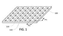
図1には、マイクロデバイス110のアレイを有する移載元基板100が示されている。マイクロデバイス110は、例えば発光ダイオード(LED)などの小型電子素子及び論理IC、プロセッサ、メモリ、コントローラなどの集積回路チップである。マイクロデバイス110はミクロンスケールのデバイスであり、例を挙げると、最大横寸法は約1〜100ミクロンである。このデバイスの横寸法は、例えば約1〜50ミクロン、例えば5〜50ミクロン、例えば10〜30ミクロンの場合があり得る。全てのマイクロデバイス110を同一に、すなわち、同一の寸法、回路パターン及びレイヤー構造にすることが可能である。
FIG. 1 shows a
図1には、移載元基板の面に平行な2つの直交方向にPX1及びPY1のピッチで、規則的な長方形アレイ状に並べられたマイクロデバイス110が示されているが、例えば千鳥アレイなどの他のアレイ構成も可能である。
FIG. 1 shows
マイクロデバイス110を移載元基板100の上に直接製造することが可能であり、例えばデバイス基板などの別の基板の上で製造しておいて、ピッチを変えることなく、移載元基板100に移載することも可能である。例えば、デバイス基板の上ではマイクロデバイスを比較的高密度に製造することが可能であり、移載元基板100を粘着テープにして、デバイスと接触させて配置することも可能である。次に、デバイス基板を取り除くか、切り離して、各マイクロデバイス110を例えば粘着テープである移載元基板に個別に取り付けることが可能である。
The
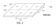
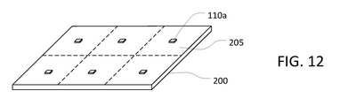
図2は、セル205のアレイを有する移載先基板200を示す。各セル205には、マイクロデバイス110を収容するスポット210がある。したがって、スポット210もアレイ状に配置されている。しかし、移載先基板200上のスポット210のアレイの間隔は、移載元基板100上のマイクロデバイス110の間隔とは異なる場合がある。通常は、スポット210間の間隔は、移載元基板100上のマイクロデバイス110間の間隔よりも大きい。例えば、図2には、移載先基板200の面に平行な2つの直交方向にPX2及びPY2のピッチで、長方形アレイ状に並べられたスポット210が示されている。したがって、ピッチPX2はピッチPX1よりも大きく、ピッチPY2はピッチPY1よりも大きい場合がある。上記のように、例えば千鳥アレイなどの他のアレイ構成も可能である。スポット210間の間隔はマイクロデバイス110間の間隔とは異なるので、マイクロデバイスをひとまとめに移載しようとして、移載元基板100を単純に移載先基板200に当接させて置くことはできない。
FIG. 2 shows a
図2に示されていないが、移載先基板100は、特にそれが製品の一部を形成することになる基板である場合には、正しくスポット210に固定された時に、マイクロデバイス110に電力を供給するために、及び/又はマイクロデバイス110をアドレス指定するために、及び/又はマイクロデバイス110を制御するために、回路及び他の構成部品を備えることができる。例えば、各スポット210は、マイクロデバイス110の1つ以上のボンドパッドに電気的に接続するボンドパッドを1つ以上備えることができる。
Although not shown in FIG. 2, the
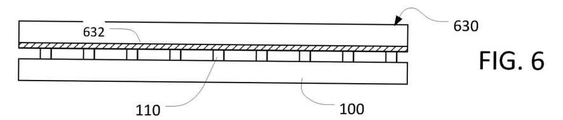
図11Aは移載元基板から移載先基板へマイクロデバイスを移載するためのシステムの概略側面断面図である。図11Aには、移載元基板100から移載先基板200へマイクロデバイスを移載するためのシステム600が示されている。議論のため、Z軸を基板100、200の平面に対して垂直な方向、X軸及びY軸を基板400の平面に平行な2つの直交する方向とする。通常は、Z軸は鉛直軸、すなわち重力の方向と一致する軸であるが、このことは必須ではない。
FIG. 11A is a schematic side sectional view of a system for transferring a microdevice from a transfer source substrate to a transfer destination substrate. FIG. 11A shows a
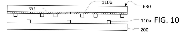
装置600は、移載元基板100を支持するステージ610、移載先基板200を支持するステージ510、及び移載装置630を備える。移載装置630は、粘着層420を配置することが可能な表面632を備える。移載装置630は、入れ替え可能な移載基板420を備えることが可能であり、この移載基板に粘着層420が形成される。選択的に、表面632は、移載装置630と一体になっている部分でもよい。
The
表面632は平面、例えば平板の底部とすることができ、ステージ610、510の上面と平行にすることができる。選択的に、表面632は円筒形、例えば回転ドラムの外面とすることができる。
The
1つ以上のアクチュエータが、移載装置630と、ステージ610及び620との間の相対動作を提供する。例えば、移載装置630は、表面632をX軸、Y軸及びZ軸に沿って移動させることができる3軸ロボットアーム512を備えることができる。しかし、他にも多くの構成が可能である。例えば、ロボットアーム512はY軸及びY軸の運動のみを提供すると共に、ステージ610、620が垂直に移動可能であるか、又は、両ステージはY軸に沿って移動可能である場合などの構成が可能である。移載装置630が交換可能な移載基板410を備えるならば、ロボットアーム512はその移載基板を保持するためのエンドエフェクタを備えてもよい。このエンドエフェクタは、真空チャック又は端縁把持用アクチュエータでもよい。
One or more actuators provide relative movement between the
装置600はまた、表面632に接する粘着層420の一部を選択的に「無効化」するためのシステムを備える。この文脈において、「無効化」には、例えば溶解又は溶融によって粘着層を完全に除去すること、又はその材料の物理的性質を改変して、粘着層がもはや粘着性を持たなくなる(「変性される」とも呼ばれる)ことのいずれかが含まれている。そのシステムを、表面632を備える物体の背面に光源からの光を選択的に向ける照射システム530とすることができる。選択的に、そのシステムは、表面632を備える物体に埋め込まれた、個別に制御可能なヒーターを備えてもよい。
The
プログラム可能なコンピュータなどのコントローラ650は、装置の各種構成要素、例えばアクチュエータ及び照射システムの動作を調整する。動作にあたっては、表面632に接する粘着層420は、移載元基板100上のマイクロデバイス110と接触するように降ろされて、そのマイクロデバイスと共に持ち上げられる。粘着層420上のマイクロデバイス110は、移載先基板200の上まで横に移動して、移載先基板200の上に降ろされる。次に、選択された領域内の粘着層が無効化され、表面632は、残った粘着層420と共に移載先基板200から離れて持ち上げられて、マイクロデバイスは、粘着層が無効化された領域に対応する移載先基板上のスポットに残ったままになる。上記の説明では、表面632が相対動作を提供するものとして表現されているが、ステージ610、620の動作が必要な相対動作の一部又は全部を提供することも可能であることが理解されよう。
A
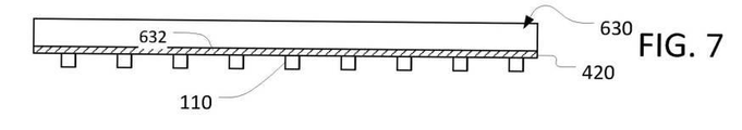
図3は、移載元基板から移載先基板へ複数のマイクロデバイスを移載する方法300のフロー図である。図4〜10は、移載元基板から移載先基板へ複数のマイクロデバイスを移載する方法を説明する概略側面断面図である。 FIG. 3 is a flow chart of a method 300 for transferring a plurality of microdevices from a transfer source substrate to a transfer destination substrate. 4 to 10 are schematic side sectional views illustrating a method of transferring a plurality of microdevices from the transfer source substrate to the transfer destination substrate.
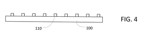
図4に示されるように、マイクロデバイス110のアレイを有する移載元基板100を製造するか、又は製造工場から受け取る。(ステップ304)
As shown in FIG. 4, a
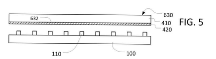
図5に示されるように、移載元基板100は、移載装置630の表面632に近接して位置決め配置される(ステップ308)。移載元基板の方向を合わせることで、移載装置630と向かい合う移載元基板100の面にマイクロデバイス110が来る。移載装置は、粘着層420を備える。粘着層420は、着脱可能な移載基板400の一部とすることができる。粘着層420は、例えば未硬化又は部分的に硬化したポジ型フォトレジストなどの粘着性ポリマーでもよい。
As shown in FIG. 5, the
粘着層420は、少なくともマイクロデバイス110のアレイに対応する表面632の部分の全体にわたって延在する。いくつかの実施形態では、粘着層420は、全マイクロデバイス110にまたがる連続した単一層である。このような単一層の利点は、移載元基板100に対して移載装置630を横方向に正確に位置決めする必要がないことである。いくつかの実施形態では、粘着層632は複数の別々の島状に分割され、各島がマイクロデバイス110の1つずつに対応している。しかし、そのような実施形態では、移載装置630を横方向に位置決めして、島を移載元基板100上のマイクロデバイス110に接触させる必要がある。
The
スピンコーティング又は液滴吐出型描画法によって移載装置630の表面632に粘着層420を塗布できる。例えばバッキング基板410のような表面632を備える物体の材料は、例えばガラス又は石英のように、粘着層420を硬化又は溶解するために使用される光の波長に対して実質的に透明な材料である。
The
図5では、粘着層420が連続層として示されているが、このことは必須ではない。例えば、移載元基板110上のマイクロデバイス110の位置に対応する個々のスポットに、又は縞模様状や他のパターンで、粘着層420を塗布できる。
In FIG. 5, the
次に、図6に示されるように、移載装置630を移載元基板100に近接して配置して、マイクロデバイス110を粘着層420に付着させる(ステップ312)。
Next, as shown in FIG. 6, the
図5、6に示される方法の代替方法として、粘着層420を移載元基板100上に直接堆積させて、粘着材料が少なくともマイクロデバイス110を覆うことが可能である。例えば、粘着材料の全面連続層420を、少なくともマイクロデバイス110のアレイの全体にわたって堆積させることができる。次いで、移載装置630の表面632を下降させて粘着層420と接触させることができる。
As an alternative to the method shown in FIGS. 5 and 6, the
図7に示されるように、ここで、移載元基板100を取り除いて(ステップ316)、マイクロデバイス110を移載装置630の粘着層420に取り付けた状態にしておくことができる。例えば、レーザ装置などの赤外線熱源を使用して、各マイクロデバイス110が移載元基板100に取り付けられている領域を溶融することで、マイクロデバイス110から移載元基板100を取り外すことができる。
As shown in FIG. 7, here, the
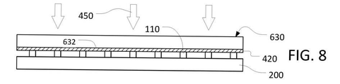
図8を参照する。移載装置630を位置決め配置して、マイクロデバイス110を移載先基板200と接触させて置くことが可能である(ステップ320)。
See FIG. The
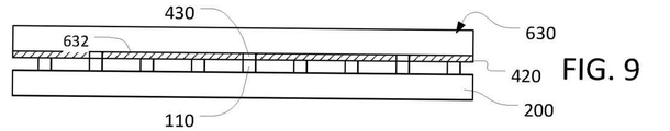
図8及び図9を参照する。移載先基板200に引き渡されるべきマイクロデバイス110に対応する、粘着層420の選択された領域430に、例えば除去や変性などの無効化が施される(ステップ324)。例えば、光450は、例えばバッキング基板410などの表面632を備える物体を通過して、領域430に選択的に向けられ得る。光は、粘着層420の領域430を溶融又は溶解することができ、あるいは領域430を非粘着性組成物に硬化させることができる。いくつかの実施形態では、光は粘着層420を露光し、その露光部分は現像液で除去される。
8 and 9 are referenced. The selected
図11Bは、移載基板400から移載先基板200へマイクロデバイスを移載するための装置500の例を示している。議論のため、Z軸を移載基板400の平面に対して垂直な方向、X軸及びY軸を移載基板400の平面に平行な2つの直交する方向とする。通常は、Z軸は鉛直軸、すなわち重力の方向と一致する軸であるが、このことは必須ではない。
FIG. 11B shows an example of a
装置500は移載先基板200を支持するステージ510と、移載基板400を保持する、例えば端縁把持用アクチュエータなどのホルダ520を備える。リニアアクチュエータなどのアクチュエータ512によって、ステージ510とホルダ520との間にZ軸に沿う相対動作が提供される。図示されるように、アクチュエータ512を連結し、かつ構成して、ホルダ520が静止している状態を維持すると共に、ステージ510をZ軸に沿って移動させることが可能である。また、その逆も同様に可能である。
The
いくつかの実施形態では、1つ以上の追加アクチュエータによって、ステージ510とホルダ520の間にX軸及びY軸に沿う相対動作が提供される。ここでも再び、そのアクチュエータを連結し、かつ構成して、ホルダ520が静止している状態を維持すると共に、ステージ510をX−Y平面内で移動させることが可能である。また、その逆も同様に可能である。例えば、X−Y平面内での動作を提供するロボットアームにホルダ520を位置決め配置することができる。
In some embodiments, one or more additional actuators provide relative movement along the X and Y axes between the
装置500はまた、照射システム530を備える。照射システム530は、光源532と、光源からの光を選択的に移載基板400の背面に向ける機構とを備える。ある実施形態では、照射システム530は、独立して制御可能なミラー、例えばデジタルマイクロミラーデバイス(DMD)534の二次元アレイを備える。照射システム530はまた、光源532からの光をDMD534に向けるための照射光学系536、及び/又は、DMD534の駆動ミラーによって反射された光を粘着層420に向けるための投影光学系538を備えることができる。DMD534のどのミラーを作動させるかを制御することによって、光450を所望の領域430に選択的に向けることができる。
The
図11Cを参照する。DMD534は複数の独立したミラー550を備えることができる。例えばミラー550aによって示される第1の位置と、例えばミラー550bによって示される第2の位置との間で、各ミラー550を独立して傾けることが可能である。第1の位置では、光源532からの入射光は、反射されて投影光学系538に送られ、結像面内の特定の画素(例えば移載基板400に接する粘着層)を照射し、第2の位置では、光源532からの入射光は、反射光が結像領域(例えば移載基板400に接する粘着層)に到達しない経路に沿って反射される。個々のミラー550を制御するために回路が形成される基板554の上の支柱552で、ミラー550を支持することができる。しかし、それ以外にも多くの形式がDMDには可能である。
See FIG. 11C. The
光源532は、例えば水銀アーク灯などのアーク灯、又は、例えば固体レーザダイオードなどのレーザ装置とすることができる。一群の光ファイバーの束の一方の端を、1つ以上のレーザダイオードに接続することが可能であり、その光ファイバーの他方の端からの光を照射光学系536に向けるか、又は直接DMD534に送ることも可能である。
The
DMDを備える照射システムに関する更なる議論は、米国特許出願公開第2016/0282728号、第2016/0219684号、第2016/0124316号に記載されている。特に、米国特許公開第2016/0124316号は、照射−投影ビームセパレータを備える光学システムについて述べており、その照射−投影ビームセパレータを使用して光源532からの光をDMD534に向け、反射した光450を分離することが可能である。
Further discussion of irradiation systems with DMDs is described in US Patent Application Publication Nos. 2016/0282728, 2016/0219684, 2016/01/24316. In particular, US Patent Publication No. 2016/0124316 describes an optical system comprising an irradiation-projection beam separator, which is used to direct light from a
いくつかの実施形態では、投影光学系538の視野は、移載基板400の全体に及ぶ。この場合には、光450と移載基板400との間で横方向の動作を行う必要はない。しかし、いくつかの実施形態では、投影光学系538の視野は、移載基板400の一部にしか及ばない。この場合には、アクチュエータが、移載基板400の露光の各間に、照射システム530と移載基板400との間のX−Y平面内の相対動作を提供することが可能である。
In some embodiments, the field of view of the projection
照射システム530は、ミラーの二次元アレイではなく、むしろミラーの直線アレイを備え、アクチュエータが照射システム530と移載基板400との間のX−Y平面内の相対動作を提供し、移載基板400の全域にわたってミラーの直線アレイを走査させることが可能である。選択的に、照射システム530は、ミラーの直線アレイを備え、例えばガルバノスキャナなどのアクチュエータで直線DMDアレイ534を回転させ、結果として生じる反射光を移載基板400の全域にわたって走査させることが可能である。
The
別の実施形態として、例えばレーザ装置からの光ビームを移載基板400の全域にわたってラスタ走査させ、走査に伴ってDMDと同じ機能を提供しながら、その光ビームを変調することが可能である。例えば、照射システム430は、2つの直交軸の周りに1つのミラーを回転させることができる2軸ミラージンバルを備えることで、光ビームを移載基板上で2つの直交軸に沿って走査させることが可能である。別の実施例として、照射システム430は、2つのガルバノミラースキャナを(光ビームの経路に沿って)直列に備えることができ、これによって、光ビームを移載基板上で2つの直交軸に沿って走査させることが可能になる。
In another embodiment, for example, a light beam from a laser device can be raster-scanned over the entire area of the
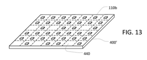
図10及び図12〜13に示されるように、選択された領域430が照射されたならば、移載装置630は持ち上げられ、選択されたマイクロデバイス110aは移載先基板200上の所定の位置に残されたままになる(ステップ328)。粘着層430が露光されなかった位置に残ったマイクロデバイス110bは、移載基板400に接した状態を維持している。
As shown in FIGS. 10 and 12-13, if the selected
図1−2及び図12−13を参照する。移載元基板100上でのマイクロデバイスの初期の空間密度は、上記故に移載装置630上での空間密度も、移載先基板200上のスポット210の空間密度よりも大きい。しかし、スポット210と移載基板上の特定のマイクロデバイス110の位置が合うならば、スポット210に対応するマイクロデバイス110だけを移載することができる。例えば、ピッチPX2がピッチPX1の整数倍であり、ピッチPY1がピッチPX2の整数倍である場合、(PX2*PY2)/(PX1*PY1)個のマイクロデバイス110毎に1個が移載される。長方形アレイでは、PX2/PX1列毎、及びPY2/PY1行毎に、移載されたマイクロデバイス110が位置決め配置され得る。
See FIGS. 1-2 and 12-13. The initial spatial density of the microdevice on the
図13に示されるように、その結果である移載装置630’には、マイクロデバイス110bが欠けているセル440が存在することになる。しかし、移載装置630’は、別の移載先基板200で再利用が可能である。手短に言えば、ステップ320、324、328を繰り返すことができるが、別の移載先基板を用いて、さらに移載装置630から別組のマイクロデバイスを使用する必要がある。すなわち、移載装置630’を新しい移載先基板に近接させて位置決め配置することができるが、別組のマイクロデバイスをスポット120と位置決め配置する必要がある。例えば、移載装置630’を各繰り返しにつき1セルだけ移動させることができる。これにより、理想的には、長方形アレイでは、移載装置630を合計で(PX2×PY2)/(PX1×PY1)回、使用することが可能になる。
As shown in FIG. 13, the resulting transfer device 630'will have
図14に示されるように、いくつかの製品では、各セル205内に異なる種類の複数のマイクロデバイス110i、110j、110kが必要になる場合がある。例えば、カラーLEDディスプレイの場合には、赤色、青色、緑色のそれぞれに1個ずつ、合計3個のマイクロLEDが必要になることがある。各マイクロLEDは、1つのサブピクセルを提供することができる。サブピクセルには様々なパターンが可能である。例えば、異なる色のサブピクセルを単純に単一の行又は列に配置することができる。選択的に、例えば、セル内のサブピクセルを、例えば赤色及び緑色の2つの色を別個に持つ2つのサブピクセルと、例えば青色である第3の色の単一サブピクセルとで、五の目型パターンに配置することができる(このパターンはまた、ペンタイルアレイとして知られている)。これらの移載技術を用いて、4色以上のサブピクセルを有するディスプレイ、例えば、赤色、緑色、青色及び黄色のマイクロLEDを有するディスプレイを形成することも可能である。
As shown in FIG. 14, some products may require a plurality of different types of
こうした異なる色のLEDは、異なる色の光を放射する蛍光体層を有するLEDであってもよい。又は、異なる色のフィルタ層を有するLEDであってもよい。又は、白色光を放射するが、白色光を吸収して異なる色の光を再放射するオーバーレイ用蛍光体材料(この材料は量子ドットでもよい)も備えるLEDであってもよい。 Such a different color LED may be an LED having a phosphor layer that emits light of a different color. Alternatively, it may be an LED having a filter layer of a different color. Alternatively, the LED may also include an overlay phosphor material (which may be quantum dots) that emits white light but absorbs white light and re-radiates light of a different color.
異なるマイクロデバイス、例えば異なる色のマイクロLEDを、移載先基板に必要とされる空間密度よりも高い空間密度で別々の移載元基板上に製造できる。その後、各移載元基板に対して移載プロセスを実行できる。すなわち、それぞれ特定の移載元基板から得られたマイクロデバイスを、それ自体の移載基板へ移載することができる。例えば、青色のマイクロLEDを載せた移載基板、赤色のマイクロLEDを載せた移載基板、及び緑色のマイクロLEDを載せた移載基板があり得る。各移載基板では、各セルに対して1個のマイクロデバイスが移載先基板へ移載される。 Different microdevices, such as microLEDs of different colors, can be manufactured on different source substrates with a higher spatial density than required for the destination substrate. After that, the transfer process can be executed for each transfer source board. That is, the microdevices obtained from each specific transfer source substrate can be transferred to the transfer substrate itself. For example, there may be a transfer board on which a blue micro LED is mounted, a transfer board on which a red micro LED is mounted, and a transfer board on which a green micro LED is mounted. In each transfer board, one microdevice is transferred to the transfer destination board for each cell.
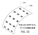
図15に示されるように、いくつかの実施形態では、移載先基板200はフレキシブル基板である。例えば、移載先基板200をフレキシブル回路として、マイクロデバイス110をマイクロLEDとすることで、フレキシブルディスプレイスクリーンを提供することができる。選択的に、又は、それに加えて、移載先基板200を伸縮性基板とすることができる。
As shown in FIG. 15, in some embodiments, the
上記の説明は、移載元基板には(したがってターゲット基板にも)、移載先基板上の各セルでの移載先スポットと適切に位置が合わさるマイクロデバイスがあると仮定していた。これにより、1回の解放操作で全てのマイクロデバイスを移載基板から移載先基板に移載することが可能になる(すなわち、粘着層の対応する全領域を同時に露光する)。 The above description has assumed that the source board (and therefore also the target board) has microdevices that are properly aligned with the destination spots in each cell on the destination board. This makes it possible to transfer all microdevices from the transfer substrate to the transfer destination substrate in a single release operation (ie, simultaneously expose the entire corresponding area of the adhesive layer).
しかし、移載元基板上のマイクロデバイス間の間隔が、1回の解放操作で全てのマイクロデバイスを移載先スポットに移載することが不可能な間隔になっている場合があり得る。例えば、ピッチPX2がピッチPX1の整数倍ではない場合、及び/又はピッチPY1がピッチPX2の整数倍ではない場合がある。 However, the spacing between the microdevices on the transfer source substrate may be such that it is not possible to transfer all the microdevices to the transfer destination spot with a single release operation. For example, pitch PX2 may not be an integral multiple of pitch PX1 and / or pitch PY1 may not be an integral multiple of pitch PX2.
それでも、少なくとも個々のマイクロデバイスをピックアンドプレースしなければならない場合と比較すると、製造スループットの大幅な向上を達成することは、依然として可能である。図16を参照する。改良プロセスでは、移載元基板上のマイクロデバイスの当初の間隔に対して任意の間隔を有する長方形アレイにマイクロデバイスを配置することが可能になる。 Nevertheless, it is still possible to achieve significant improvements in manufacturing throughput, at least when compared to having to pick and place individual microdevices. See FIG. The improvement process allows the microdevices to be placed in a rectangular array with any spacing relative to the initial spacing of the microdevices on the source board.
最初に、マイクロデバイス110が、移載元基板から第1の移載装置の第1の表面、例えば第1の移載基板400aに移載される。マイクロデバイス110は、X軸に沿うピッチPX1及びY軸に沿うピッチPY1で第1の移載基板110上に並べられている。次に、第2の移載装置の第2の表面、例えば第2の移載基板400bに第1の移載基板400aを近接させて位置決め配置する。全てのマイクロデバイスを一度に第2の移載基板に移載するのではなく、一度に1列だけが移載されるが、この時、第1の移載基板には移載の各間に横方向の再位置決め配置が行われて、一方の方向に適切な間隔がもたらされる。続いて、マイクロデバイスは、一度に1行ずつ、第2の移載基板から移載先基板に移載されるが、この時、第1の移載基板には移載の各間に横方向の再位置決め配置が行われて、他の方向に適切な間隔がもたらされる。
First, the
例えば、移載先基板にはN行M列のセルがあって、マイクロデバイス110を収容すると仮定する。第1の移載基板400aは、第2の基板400bに近接して位置決め配置される。照射システムを制御して、単一列内のN個のマイクロデバイス110に対応する領域を照射する。したがって、N個のマイクロデバイス110を含む1列だけが第2の移載基板400bに移載されることになる。次に、第1の移載基板400aを第2の移載基板400bに対してX軸に沿って移動させ、照射システムを制御して別の単一列内の別のN個のマイクロデバイス100に対応する領域を照射することで、N個のマイクロデバイスの列がもう1列、配置される。N行のマイクロデバイスを有するM列が第2の移載基板400bに移載されるまで、この移動と配置のプロセスがM−1回繰り返される。第2の移載基板400bに対する第1の移載基板400aの移動量は、第2の移載基板400b上のX軸に沿ったマイクロデバイスのピッチが、移載先基板の所望のピッチPX2と一致するピッチになる移動量である。Y軸に沿ったマイクロデバイスのピッチは、PY1又はPY1の整数倍であればよい。
For example, it is assumed that the transfer destination substrate has cells of N rows and M columns and accommodates the
N行のマイクロデバイスを有するM列のアレイが第2の移載基板400bに移載されたならば、マイクロデバイス110を移載先基板200に移載することができる。第2の移載基板400bは、第2の基板400bに近接して位置決め配置される。照射システムを制御して、単一行内のM個のマイクロデバイス110に対応する領域を照射する。したがって、M個のマイクロデバイス110を含む単一行だけが移載先基板200に移載されることになる。次に、第2の移載基板400bを移載先基板400bに対してY軸に沿って移動させ、照射システムを制御して別の単一行内の別のM個のマイクロデバイス100に対応する領域を照射することで、M個のマイクロデバイスの行がもう1行、配置される。M列のマイクロデバイスを有するN行が移載先基板200に移載されるまで、この移動と配置のプロセスがN−1回繰り返される。移載先基板200に対する第2の移載基板400bの移動量は、移載先基板200上のY軸に沿ったマイクロデバイスのピッチが、移載先基板200の所望のピッチPY2と一致するピッチになる移動量である。その結果、移載先基板上のマイクロデバイスのピッチは、PX1とPX2の関係及びPY1とPY2の関係は際限なく自由でありながらも、今やX軸方向にPX2、Y軸方向にPY2になっている。
If the M-column array with N rows of microdevices is transferred to the
この多段階移載プロセスの利点は、移載工程の総回数が概ねM+Nになっていることである。高解像度ディスプレイでは、この合計数M+Nは依然として多い数かも知れないが、個別ピックアンドプレース法に必要とされるであろう移載工程の数、すなわちM*Nよりは遙かに少ない。 The advantage of this multi-step transfer process is that the total number of transfer steps is approximately M + N. For high resolution displays, this total number of M + N may still be high, but much less than the number of transfer steps that would be required for the individual pick-and-place method, namely M * N.
いくつかの実施形態では、マイクロデバイスは、移載先基板に移載される前に点検又は検査を受けることになる。マイクロデバイスがまだ移載元基板上にある時に検査が行われることもあり、マイクロデバイスが移載基板上にある時に点検が行われることもある。点検又は検査によってマイクロデバイスに欠陥があることが明らかになった各セルには、移載システムの照射システムを制御して、欠陥のあるマイクロデバイスに対応する移載基板の領域を照射しない。したがって、識別された欠陥のあるマイクロデバイスは、移載先基板に移載されない。こうしてマイクロデバイスを欠くことになった移載先基板上のセルは、どれもがその後のピックアンドプレース操作で機能するマイクロデバイスを収容することができる。これにより、移載先基板を、故に製品をも、非常に高い歩留まりで製造することが可能になる。 In some embodiments, the microdevice will be inspected or inspected before being transferred to the destination substrate. The inspection may be performed when the microdevice is still on the transfer source board, or it may be inspected when the microdevice is on the transfer board. Each cell that has been found to be defective by inspection or inspection does not control the irradiation system of the transfer system to irradiate the area of the transfer substrate corresponding to the defective microdevice. Therefore, the identified defective microdevice is not transferred to the destination substrate. Any cell on the destination board that thus lacks the microdevice can accommodate the microdevice that will function in subsequent pick-and-place operations. This makes it possible to manufacture the transfer destination substrate, and therefore the product, with a very high yield.
いくつかの実施形態では、マイクロデバイスのどちらの面を移載先基板と接触させる必要があるかに応じて、マイクロデバイスを裏返すために、そのマイクロデバイスを第3の移載基板に移載することが必要になる(第3の移載基板への移載が、第1の移載基板の前、第2の移載基板の後、又は第1の移載基板と第2の移載基板との間ということもあり得る)。 In some embodiments, the microdevice is transferred to a third transfer board in order to turn the microdevice over, depending on which side of the microdevice needs to be in contact with the transfer destination board. (The transfer to the third transfer board is before the first transfer board, after the second transfer board, or between the first transfer board and the second transfer board. It can be between).
上記の方法は単一のマイクロデバイスの表面実装方法を説明しているが、この方法は2つ以上のマイクロデバイスを含み得ることを理解すべきである。 Although the above method describes a surface mount method for a single microdevice, it should be understood that this method can include more than one microdevice.
コントローラは、デジタル電子回路、コンピュータソフトウェア、ファームウェア、ハードウェア、又はそれらの組み合わせで実現される。コントローラは、1つ以上のコンピュータプログラム製品を、すなわち例えば非一時的な機械読取り可能記録媒体又は伝搬信号などの情報媒体に明白に具体化される1つ以上のコンピュータプログラムを備えることができる。そして、例えばプログラム可能なプロセッサ、コンピュータ又は複数のプロセッサなどのデータ処理装置、若しくは複数のコンピュータによって実行すること、又はこれら機器の操作の制御を行うことができる。コンピュータプログラム(プログラム、ソフトウェア、ソフトウェアアプリケーション、又はコードとも呼ばれる)は、コンパイル言語又はインタープリター言語を含む任意の形式のプログラミング言語で書かれてもよく、スタンドアロンプログラムや、あるいはモジュール、コンポーネント、サブルーチン、その他コンピュータ環境での使用に適した他の構成単位を含むどのような形式でも導入され得る。コンピュータプログラムは、1台のコンピュータで、若しくは1つのサイトにある、又は複数のサイトにわたって分散しているが通信ネットワークによって相互に接続されている、複数台のコンピュータで実行されるように、導入され得る。 The controller is realized by digital electronic circuits, computer software, firmware, hardware, or a combination thereof. The controller can include one or more computer program products, i.e., one or more computer programs that are expressly embodied in an information medium such as a non-temporary machine readable recording medium or a propagating signal. Then, for example, it can be executed by a programmable processor, a data processing device such as a computer or a plurality of processors, or a plurality of computers, or can control the operation of these devices. Computer programs (also called programs, software, software applications, or code) may be written in any form of programming language, including compilation or interpreter languages, and may be stand-alone programs or modules, components, subroutines, etc. It can be deployed in any format, including other building blocks suitable for use in a computer environment. Computer programs are introduced to run on one computer, or on multiple computers at one site, or distributed across multiple sites but interconnected by communication networks. obtain.
本明細書に記載されたプロセス及び論理フローは、1つ以上のコンピュータプログラムを実行する1つ以上のプログラマブルプロセッサによって実行されて、入力データに基づく動作と出力の生成とによる機能が発揮され得る。例えばFPGA(フィールドプログラマブルゲートアレイ)又はASIC(特定用途向け集積回路)などの専用ロジック回路によって、それらプロセス及び論理フローを実行することも可能であり、そうした専用ロジック回路として装置を実現することも可能である。 The processes and logic flows described herein can be performed by one or more programmable processors running one or more computer programs to perform functions based on input data and generate outputs. For example, it is possible to execute those processes and logic flows by a dedicated logic circuit such as FPGA (field programmable gate array) or ASIC (application specific integrated circuit), and it is also possible to realize a device as such a dedicated logic circuit. Is.
鉛直や横といった位置決め配置に関する用語を使用してきた。しかし、そのような用語は、重力に対する絶対的な位置決め配置ではなく、相対的な位置決め配置を指すことを理解されたい。例えば、横方向とは基板表面に平行な一方向であり、それに対して、鉛直方向は基板表面に垂直な方向である。 We have used terms for positioning such as vertical and horizontal. However, it should be understood that such terms refer to relative positioning arrangements rather than absolute positioning arrangements with respect to gravity. For example, the horizontal direction is one direction parallel to the surface of the substrate, whereas the vertical direction is the direction perpendicular to the surface of the substrate.
当業者には、上記の例が例示を意図したものであって、限定を意図したものではないことが理解されるであろう。本明細書を読み、図面を検討した当業者には明白である、これらの例に対する全ての置換、強化、等価物及び改良は、本開示の真の趣旨及び範囲に含まれることが意図されている。したがって、添付された以下の特許請求項は、これらの教示の真の趣旨及び範囲に含まれる、このような全ての変更、置換及び等価物を含むことが意図されている。 Those skilled in the art will appreciate that the above examples are intended as illustrations, not limitations. All substitutions, enhancements, equivalents and improvements to these examples, apparent to those skilled in the art who have read the specification and reviewed the drawings, are intended to be included in the true spirit and scope of the present disclosure. There is. Accordingly, the following claims in attachment are intended to include all such modifications, substitutions and equivalents within the true intent and scope of these teachings.
Claims (9)
移載先基板を保持するための第1の支持体と、
その表面に形成された連続粘着層を有する移載体と、
前記移載体を提供又は保持するための第2の支持体と、
前記第1の支持体と前記第2の支持体の互いに対する相対動作を提供するように構成された1つ以上のアクチュエータと、
前記移載体の前記連続粘着層の領域を選択的にかつマスクを使用せずに露光するように構成された照射システムであって、
前記照射システムはデジタルマイクロミラーの二次元アレイ及び光学系を備え、
前記デジタルマイクロミラーの二次元アレイ及び光学系は、前記デジタルマイクロミラーの二次元アレイからのイメージが前記移載体全体に及ぶような視野を有している、照射システムと、
コントローラであって、
前記1つ以上のアクチュエータに相対動作を生じさせることで、前記連続粘着層に取り付けられた複数のマイクロデバイスを前記移載先基板に接触させ、
前記照射システムに選択的に前記連続粘着層の1つ以上の部分を露光させることで、前記視野内の前記連続粘着層の前記1つ以上の部分のすべてを同時に露光しながら、1つ以上の無効化された部分を作り出し、
前記1つ以上のアクチュエータに相対動作を生じさせることで、前記表面と前記移載先基板が互いに離れ、前記連続粘着層の前記1つ以上の無効化された部分に対応する1つ以上のマイクロデバイスが前記移載先基板上に残るように構成されたコントローラと、
移載元基板を保持する第3の支持体であって、
前記1つ以上のアクチュエータは、前記第2の支持体と前記第3の支持体の互いに対する相対動作を提供するように構成され、
前記コントローラは、前記1つ以上のアクチュエータに前記移載元基板と前記移載体の互いに対する相対動作を生じさせることで、前記複数のマイクロデバイスが前記移載元基板上にあるときに前記移載体の前記表面の前記連続粘着層が前記複数のマイクロデバイスに接触して、前記複数のマイクロデバイスが前記移載体の前記連続粘着層に付着するように構成されている、第3の支持体と、
前記マイクロデバイスから前記移載元基板を分離するためのエネルギー源とを備える装置。 A device for positioning and arranging microdevices on the transfer destination board.
A first support for holding the transfer destination board,
A transfer body having a continuous adhesive layer formed on its surface,
A second support for providing or holding the transfer,
One or more actuators configured to provide relative movement of the first support and the second support with respect to each other.
An irradiation system configured to selectively and without the use of a mask to expose the region of the continuous adhesive layer of the transfer body .
The irradiation system includes a two-dimensional array of digital micromirrors and an optical system.
The two-dimensional array and optical system of the digital micromirror have a field of view such that the image from the two-dimensional array of the digital micromirror covers the entire transfer body, and the irradiation system.
It ’s a controller,
By causing the one or more actuators to move relative to each other, a plurality of microdevices attached to the continuous adhesive layer are brought into contact with the transfer destination substrate.
By selectively exposing one or more portions of the continuous adhesive layer to the irradiation system, one or more portions of the continuous adhesive layer in the visual field are simultaneously exposed while simultaneously exposing one or more portions of the continuous adhesive layer . Create an invalidated part,
By causing the one or more actuators to move relative to each other, the surface and the transfer destination substrate are separated from each other, and one or more micros corresponding to the one or more invalidated portions of the continuous adhesive layer. A controller configured so that the device remains on the destination board,
A third support that holds the transfer source board,
The one or more actuators are configured to provide relative movement of the second support and the third support with respect to each other.
The controller causes the one or more actuators to cause the transfer source board and the transfer body to operate relative to each other, so that the transfer body can be used when the plurality of microdevices are on the transfer source board. A third support configured such that the continuous adhesive layer on the surface of the surface is in contact with the plurality of microdevices and the plurality of microdevices are attached to the continuous adhesive layer of the transfer body.
A device including an energy source for separating the transfer source substrate from the microdevice .
前記ロボットアームは、前記第3の支持体と前記第1の支持体との間で前記移載体を移動させるように動作可能になっている、請求項1に記載の装置。 The second support is provided with a robot arm to hold the transfer body.
The device according to claim 1, wherein the robot arm is movable so as to move the transfer body between the third support and the first support.
移載先基板を保持するための第1の支持体と、
その表面に形成された連続粘着層を有する移載体と、
前記移載体を提供又は保持するための第2の支持体と、
前記移載体と前記第1の支持体の互いに対する相対動作を提供するように構成された1つ以上のアクチュエータと、
光ビームを発生させる光源と、
前記光ビームを前記移載体の前記連続粘着層に調節可能に当てるように構成されたデジタルマイクロミラーの二次元アレイ及び光学系であって、前記デジタルマイクロミラーの二次元アレイからのイメージが前記移載体全体に及ぶような視野を有するデジタルマイクロミラーの二次元アレイ及び光学系と、
コントローラであって、
前記1つ以上のアクチュエータに相対動作を生じさせることで、前記移載体の前記連続粘着層に取り付けられた複数のマイクロデバイスを前記移載先基板に接触させ、
前記光源に前記光ビームを発生させ、前記デジタルマイクロミラーの二次元アレイ及び光学系を調整して前記光ビームを前記連続粘着層に当てることで、選択的に前記連続粘着層の1つ以上の部分を露光して、前記視野内の前記連続粘着層の前記1つ以上の部分のすべてを同時に露光しながら、1つ以上の無効化された部分を作り出し、
前記1つ以上のアクチュエータに相対動作を生じさせることで、前記移載体と前記移載先基板が互いに離れて、前記連続粘着層の前記1つ以上の無効化された部分に対応する1つ以上のマイクロデバイスが前記移載先基板上に残るように構成されたコントローラと、
移載元基板を保持する第3の支持体であって、
前記1つ以上のアクチュエータは、前記第2の支持体と前記第3の支持体の互いに対する相対動作を提供するように構成され、
前記コントローラは、前記1つ以上のアクチュエータに前記移載元基板と前記移載体の互いに対する相対動作を生じさせることで、前記複数のマイクロデバイスが前記移載元基板上にあるときに前記移載体の前記表面の前記連続粘着層が前記複数のマイクロデバイスに接触して、前記複数のマイクロデバイスが前記移載体の前記連続粘着層に付着するように構成されている、第3の支持体と、
前記マイクロデバイスから前記移載元基板を分離するためのエネルギー源とを備える装置。 A device for positioning and arranging microdevices on the transfer destination board.
A first support for holding the transfer destination board,
A transfer body having a continuous adhesive layer formed on its surface,
A second support for providing or holding the transfer,
One or more actuators configured to provide relative movement of the transfer and the first support with respect to each other.
A light source that generates a light beam and
A two-dimensional array of digital micromirrors and an optical system configured to adjustably apply the light beam to the continuous adhesive layer of the transfer , wherein the image from the two-dimensional array of the digital micromirrors is transferred. A two-dimensional array of digital micromirrors and an optical system with a field of view that covers the entire body,
It ’s a controller,
By causing the one or more actuators to move relative to each other, a plurality of microdevices attached to the continuous adhesive layer of the transfer body are brought into contact with the transfer destination substrate.
By generating the light beam in the light source, adjusting the two-dimensional array of the digital micromirror and the optical system , and applying the light beam to the continuous adhesive layer, one or more of the continuous adhesive layers are selectively applied. Exposing the portions to create one or more invalidated portions while simultaneously exposing all of the one or more portions of the continuous adhesive layer in the field of view.
By causing the one or more actuators to move relative to each other, the transfer body and the transfer destination substrate are separated from each other, and one or more corresponding to the one or more invalidated portions of the continuous adhesive layer. The controller configured so that the microdevice remains on the transfer destination board, and
A third support that holds the transfer source board,
The one or more actuators are configured to provide relative movement of the second support and the third support with respect to each other.
The controller causes the one or more actuators to cause the transfer source board and the transfer body to operate relative to each other, so that the transfer body can be used when the plurality of microdevices are on the transfer source board. A third support configured such that the continuous adhesive layer on the surface of the surface is in contact with the plurality of microdevices and the plurality of microdevices are attached to the continuous adhesive layer of the transfer body.
A device including an energy source for separating the transfer source substrate from the microdevice .
前記ロボットアームは、移載元基板を保持するための第3の支持体と前記移載先基板を保持するための前記第1の支持体との間で前記移載体を少なくとも横方向に移動させるように動作可能である、請求項3に記載の装置。 The second support is provided with a robot arm to hold the transfer body.
The robot arm moves the transfer body at least laterally between a third support for holding the transfer source substrate and the first support for holding the transfer destination substrate. The device according to claim 3, which is capable of operating as described above.
Applications Claiming Priority (3)
| Application Number | Priority Date | Filing Date | Title |
|---|---|---|---|
| US201662348691P | 2016-06-10 | 2016-06-10 | |
| US62/348,691 | 2016-06-10 | ||
| PCT/US2017/036804 WO2017214540A1 (en) | 2016-06-10 | 2017-06-09 | Maskless parallel pick-and-place transfer of micro-devices |
Publications (3)
| Publication Number | Publication Date |
|---|---|
| JP2019530201A JP2019530201A (en) | 2019-10-17 |
| JP2019530201A5 JP2019530201A5 (en) | 2020-07-16 |
| JP6976972B2 true JP6976972B2 (en) | 2021-12-08 |
Family
ID=60573075
Family Applications (1)
| Application Number | Title | Priority Date | Filing Date |
|---|---|---|---|
| JP2018564747A Active JP6976972B2 (en) | 2016-06-10 | 2017-06-09 | Maskless parallel pick and place transfer of microdevices |
Country Status (7)
| Country | Link |
|---|---|
| US (5) | US10153325B2 (en) |
| EP (1) | EP3469424A4 (en) |
| JP (1) | JP6976972B2 (en) |
| KR (1) | KR102427231B1 (en) |
| CN (2) | CN116047871A (en) |
| TW (2) | TWI778528B (en) |
| WO (1) | WO2017214540A1 (en) |
Families Citing this family (59)
| Publication number | Priority date | Publication date | Assignee | Title |
|---|---|---|---|---|
| JP6231432B2 (en) * | 2014-05-02 | 2017-11-15 | 富士フイルム株式会社 | Conductive film, display device including the same, and method for evaluating conductive film |
| JP6976972B2 (en) * | 2016-06-10 | 2021-12-08 | アプライド マテリアルズ インコーポレイテッドApplied Materials, Incorporated | Maskless parallel pick and place transfer of microdevices |
| US11776989B2 (en) * | 2016-06-10 | 2023-10-03 | Applied Materials, Inc. | Methods of parallel transfer of micro-devices using treatment |
| US11756982B2 (en) | 2016-06-10 | 2023-09-12 | Applied Materials, Inc. | Methods of parallel transfer of micro-devices using mask layer |
| CN106098697B (en) * | 2016-06-15 | 2019-04-02 | 深圳市华星光电技术有限公司 | Micro light-emitting diode display panel and manufacturing method thereof |
| US10978530B2 (en) * | 2016-11-25 | 2021-04-13 | Vuereal Inc. | Integration of microdevices into system substrate |
| TWI661533B (en) * | 2017-06-07 | 2019-06-01 | Asti Global Inc., Taiwan | Chip mounting system and method for mounting chips |
| US20190058081A1 (en) * | 2017-08-18 | 2019-02-21 | Khaled Ahmed | Micro light-emitting diode (led) display and assembly apparatus |
| US10511554B2 (en) | 2017-12-05 | 2019-12-17 | International Business Machines Corporation | Maintaining tribal knowledge for accelerated compliance control deployment |
| CN110120186A (en) * | 2018-02-06 | 2019-08-13 | 南京瀚宇彩欣科技有限责任公司 | Display module |
| US10593581B2 (en) * | 2018-02-26 | 2020-03-17 | Mikro Mesa Technology Co., Ltd. | Transfer head and method for transferring micro devices |
| US11637093B2 (en) * | 2018-05-24 | 2023-04-25 | Intel Corporation | Micro light-emitting diode display fabrication and assembly |
| WO2019246366A1 (en) * | 2018-06-22 | 2019-12-26 | Veeco Instruments Inc. | Micro-led transfer methods using light-based debonding |
| US10985046B2 (en) * | 2018-06-22 | 2021-04-20 | Veeco Instruments Inc. | Micro-LED transfer methods using light-based debonding |
| KR102782924B1 (en) | 2018-07-23 | 2025-03-19 | 삼성전자주식회사 | Electronic apparatus including led transmission device and controlling method thereof |
| TW202008558A (en) * | 2018-07-23 | 2020-02-16 | 飛傳科技股份有限公司 | Die transfer method and die transfer system thereof |
| US10761430B2 (en) * | 2018-09-13 | 2020-09-01 | Applied Materials, Inc. | Method to enhance the resolution of maskless lithography while maintaining a high image contrast |
| US10573544B1 (en) * | 2018-10-17 | 2020-02-25 | X-Celeprint Limited | Micro-transfer printing with selective component removal |
| US10796938B2 (en) * | 2018-10-17 | 2020-10-06 | X Display Company Technology Limited | Micro-transfer printing with selective component removal |
| CN111129057B (en) * | 2018-10-31 | 2023-06-20 | 成都辰显光电有限公司 | Micro light emitting diode array device, manufacturing method and transferring method |
| CN109524512B (en) * | 2018-11-15 | 2020-07-03 | 华中科技大学 | Method for transferring micro light-emitting diode in huge amount based on controllable micro-reflector array |
| KR102652723B1 (en) * | 2018-11-20 | 2024-04-01 | 삼성전자주식회사 | Micro led transfer device and micro led transferring method using the same |
| JP6911003B2 (en) * | 2018-12-14 | 2021-07-28 | Tdk株式会社 | Method of manufacturing element array and method of removing specific element |
| JP7319044B2 (en) * | 2018-12-14 | 2023-08-01 | Tdk株式会社 | Device array manufacturing equipment and specific device removal equipment |
| US11127720B2 (en) * | 2019-01-21 | 2021-09-21 | Nanosys, Inc. | Pixel repair method for a direct view display device |
| KR102895805B1 (en) * | 2019-01-22 | 2025-12-04 | 삼성전자주식회사 | The method for displaying visual information related to utterance input and the Electronic Device supporting the same |
| US11538786B2 (en) | 2019-03-19 | 2022-12-27 | Ordos Yuansheng Optoelectronics Co., Ltd. | Transfer printing method and transfer printing apparatus |
| EP3742477A1 (en) * | 2019-05-21 | 2020-11-25 | Nederlandse Organisatie voor toegepast- natuurwetenschappelijk Onderzoek TNO | Light induced selective transfer of components using a jet of melted adhesive |
| KR20200135069A (en) * | 2019-05-24 | 2020-12-02 | (주)포인트엔지니어링 | Micro led display manufacturing and micro led display using the same |
| US10964582B2 (en) * | 2019-06-24 | 2021-03-30 | Palo Alto Research Center Incorporated | Transfer substrate utilizing selectable surface adhesion transfer elements |
| KR20210023375A (en) * | 2019-08-23 | 2021-03-04 | 삼성전자주식회사 | Laser transffering apparatus and transffering method using the same |
| USD966207S1 (en) * | 2019-09-23 | 2022-10-11 | Star Co Scientific Technologies Advanced Research Co, Llc | Light-emitting diode array |
| CN112701076A (en) * | 2019-10-23 | 2021-04-23 | 北京小米移动软件有限公司 | Display screen manufacturing method and system |
| US11302561B2 (en) | 2019-11-12 | 2022-04-12 | Palo Alto Research Center Incorporated | Transfer elements that selectably hold and release objects based on changes in stiffness |
| CN113228243A (en) * | 2019-12-03 | 2021-08-06 | 重庆康佳光电技术研究院有限公司 | Bulk transfer method and system for semiconductor device |
| CN110993749B (en) * | 2019-12-09 | 2021-02-23 | 深圳市华星光电半导体显示技术有限公司 | Mass transfer method of micro light-emitting diode and display panel |
| EP3840030A1 (en) * | 2019-12-16 | 2021-06-23 | FRAUNHOFER-GESELLSCHAFT zur Förderung der angewandten Forschung e.V. | Massive parallel assembly method |
| KR102820198B1 (en) | 2019-12-26 | 2025-06-13 | 삼성전자주식회사 | LED transfer system and control method thereof |
| CN111128813B (en) * | 2020-01-20 | 2022-10-28 | 福州大学 | Mu LED mass transfer method |
| US12103787B2 (en) | 2020-02-18 | 2024-10-01 | Ev Group E. Thallner Gmbh | Method and device for transferring components |
| US11348905B2 (en) | 2020-03-02 | 2022-05-31 | Palo Alto Research Center Incorporated | Method and system for assembly of micro-LEDs onto a substrate |
| JP7804461B2 (en) * | 2020-03-09 | 2026-01-22 | 積水化学工業株式会社 | Method for manufacturing electronic components and method for manufacturing display devices |
| KR102754349B1 (en) * | 2020-03-20 | 2025-01-14 | 삼성전자주식회사 | Display module and repair method for display module |
| US11199774B2 (en) * | 2020-03-30 | 2021-12-14 | Canon Kabushiki Kaisha | Method and apparatus to improve frame cure imaging resolution for extrusion control |
| TWI872235B (en) * | 2020-03-30 | 2025-02-11 | 加拿大商弗瑞爾公司 | Offset alignment and repair in micro device transfer |
| EP4158683B1 (en) * | 2020-05-29 | 2024-04-10 | Erich Thallner | Method for bonding and debonding two substrates |
| US11343888B1 (en) * | 2020-12-15 | 2022-05-24 | Lumileds Llc | MicroLED power considering outlier pixel dynamic resistance |
| CN112768399B (en) * | 2021-01-11 | 2022-10-04 | 深圳市华星光电半导体显示技术有限公司 | Transfer substrate and transfer device |
| CN112968084A (en) * | 2021-02-04 | 2021-06-15 | 深圳市华星光电半导体显示技术有限公司 | Display panel and manufacturing method thereof |
| JP7387666B2 (en) * | 2021-03-15 | 2023-11-28 | 東レエンジニアリング株式会社 | Chip parts removal equipment |
| WO2023044256A1 (en) * | 2021-09-20 | 2023-03-23 | Applied Materials, Inc. | Methods of parallel transfer of micro-devices using treatment |
| TWI836592B (en) * | 2021-09-20 | 2024-03-21 | 美商應用材料股份有限公司 | Methods of parallel transfer of micro-devices using mask layer |
| WO2023086403A1 (en) * | 2021-11-11 | 2023-05-19 | Terecircuits Corporation | Photochemical and thermal release layer processes and uses in device manufacturing |
| CN114170922A (en) * | 2021-12-08 | 2022-03-11 | Tcl华星光电技术有限公司 | Display panel and method for manufacturing the same |
| WO2023108450A1 (en) * | 2021-12-15 | 2023-06-22 | 厦门市芯颖显示科技有限公司 | Addressing transfer device |
| US20240036363A1 (en) * | 2022-07-28 | 2024-02-01 | Palo Alto Research Center Incorporated | Optically activated object mass transfer apparatus |
| US20240036364A1 (en) * | 2022-07-28 | 2024-02-01 | Palo Alto Research Center Incorporated | Optically activated object mass transfer system |
| CN115356794A (en) * | 2022-09-15 | 2022-11-18 | 苏州晶方光电科技有限公司 | Imprint curing equipment, manufacturing method and application of wafer-level micro-lens array |
| JP2025099629A (en) | 2023-12-22 | 2025-07-03 | エルジー ディスプレイ カンパニー リミテッド | Display device and method for fabricating display device |
Family Cites Families (35)
| Publication number | Priority date | Publication date | Assignee | Title |
|---|---|---|---|---|
| US5467146A (en) * | 1994-03-31 | 1995-11-14 | Texas Instruments Incorporated | Illumination control unit for display system with spatial light modulator |
| JP2001305664A (en) * | 2000-04-20 | 2001-11-02 | Fuji Photo Film Co Ltd | Printer |
| JP4491948B2 (en) * | 2000-10-06 | 2010-06-30 | ソニー株式会社 | Device mounting method and image display device manufacturing method |
| JP2003005100A (en) * | 2001-06-26 | 2003-01-08 | Canon Inc | Optical modulator and projection device using the same |
| JP2003077940A (en) * | 2001-09-06 | 2003-03-14 | Sony Corp | Device transfer method, device array method using the same, and image display device manufacturing method |
| JP2004299814A (en) * | 2003-03-28 | 2004-10-28 | Takasago Thermal Eng Co Ltd | Method and apparatus for manufacturing static-free insulator substrate |
| JP4463537B2 (en) * | 2003-12-12 | 2010-05-19 | 財団法人国際科学振興財団 | Pattern exposure equipment |
| US7744770B2 (en) * | 2004-06-23 | 2010-06-29 | Sony Corporation | Device transfer method |
| JP4588428B2 (en) | 2004-12-09 | 2010-12-01 | 富士フイルム株式会社 | Image exposure method and apparatus |
| JP4686753B2 (en) * | 2004-12-14 | 2011-05-25 | 独立行政法人産業技術総合研究所 | Exposure method and exposure apparatus |
| ITMO20040332A1 (en) * | 2004-12-16 | 2005-03-16 | Windinglab S R L | SYSTEM FOR THE MULTIPLE MICROCHIP SURVEY FROM A WAFER CONSISTING OF A PLURALITY OF MICROCHIP. |
| WO2006105782A2 (en) * | 2005-04-08 | 2006-10-12 | Pac Tech-Packaging Technologies Gmbh | Method and device for transferring a chip to a contact substrate |
| JP2007025085A (en) * | 2005-07-14 | 2007-02-01 | Nikon Corp | Exposure apparatus, optical element array, multi-spot beam generator, and device manufacturing method |
| CN1963672A (en) * | 2005-11-07 | 2007-05-16 | 中芯国际集成电路制造(上海)有限公司 | Method and device for manufacturing reconfiguration mask of integrate circuit by micro electromechanical system |
| US20080122119A1 (en) * | 2006-08-31 | 2008-05-29 | Avery Dennison Corporation | Method and apparatus for creating rfid devices using masking techniques |
| JP2008122681A (en) * | 2006-11-13 | 2008-05-29 | Sony Corp | Method for mounting article, method for manufacturing light emitting diode display device, and method for temporarily fixing article intermediate to temporary fixing substrate |
| JP2010014797A (en) * | 2008-07-01 | 2010-01-21 | Nsk Ltd | Maskless exposure apparatus |
| US8506867B2 (en) | 2008-11-19 | 2013-08-13 | Semprius, Inc. | Printing semiconductor elements by shear-assisted elastomeric stamp transfer |
| WO2010113357A1 (en) | 2009-04-03 | 2010-10-07 | シャープ株式会社 | Donor substrate, process for production of transfer film, and process for production of organic electroluminescent element |
| JP5444798B2 (en) * | 2009-04-10 | 2014-03-19 | ソニー株式会社 | Device transfer method |
| JP2010251360A (en) * | 2009-04-10 | 2010-11-04 | Sony Corp | Display device manufacturing method and display device |
| WO2010132552A1 (en) * | 2009-05-12 | 2010-11-18 | The Board Of Trustees Of The University Of Illinois | Printed assemblies of ultrathin, microscale inorganic light emitting diodes for deformable and semitransparent displays |
| WO2012142177A2 (en) | 2011-04-11 | 2012-10-18 | Ndsu Research Foundation | Selective laser-assisted transfer of discrete components |
| US9555644B2 (en) | 2011-07-14 | 2017-01-31 | The Board Of Trustees Of The University Of Illinois | Non-contact transfer printing |
| US20130207544A1 (en) | 2011-09-30 | 2013-08-15 | Pinebrook Imaging Technology, Ltd. | Illumination system |
| US8518204B2 (en) * | 2011-11-18 | 2013-08-27 | LuxVue Technology Corporation | Method of fabricating and transferring a micro device and an array of micro devices utilizing an intermediate electrically conductive bonding layer |
| CN105283122B (en) * | 2012-03-30 | 2020-02-18 | 伊利诺伊大学评议会 | Appendable mountable electronics that can conform to surfaces |
| WO2013184700A1 (en) | 2012-06-04 | 2013-12-12 | Pinebrook Imaging, Inc. | An optical projection array exposure system |
| US9331230B2 (en) * | 2012-10-30 | 2016-05-03 | Cbrite Inc. | LED die dispersal in displays and light panels with preserving neighboring relationship |
| EP2917012A4 (en) | 2012-11-08 | 2016-08-10 | Ddm Systems Inc | SYSTEMS AND METHODS FOR MANUFACTURING THREE-DIMENSIONAL OBJECTS |
| KR102098261B1 (en) * | 2014-06-18 | 2020-04-08 | 엑스-셀레프린트 리미티드 | Micro assembled led displays |
| US9927723B2 (en) | 2015-03-24 | 2018-03-27 | Applied Materials, Inc. | Apparatus and methods for on-the-fly digital exposure image data modification |
| US10319697B2 (en) | 2015-05-21 | 2019-06-11 | Goertek, Inc. | Transferring method, manufacturing method, device and electronic apparatus of micro-LED |
| GB2544335A (en) * | 2015-11-13 | 2017-05-17 | Oculus Vr Llc | A method and apparatus for use in the manufacture of a display element |
| JP6976972B2 (en) | 2016-06-10 | 2021-12-08 | アプライド マテリアルズ インコーポレイテッドApplied Materials, Incorporated | Maskless parallel pick and place transfer of microdevices |
-
2017
- 2017-06-09 JP JP2018564747A patent/JP6976972B2/en active Active
- 2017-06-09 TW TW110106637A patent/TWI778528B/en active
- 2017-06-09 WO PCT/US2017/036804 patent/WO2017214540A1/en not_active Ceased
- 2017-06-09 CN CN202310084142.XA patent/CN116047871A/en active Pending
- 2017-06-09 KR KR1020197000831A patent/KR102427231B1/en active Active
- 2017-06-09 TW TW106119234A patent/TWI723178B/en active
- 2017-06-09 EP EP17811102.7A patent/EP3469424A4/en not_active Withdrawn
- 2017-06-09 US US15/619,173 patent/US10153325B2/en active Active
- 2017-06-09 CN CN201780032280.6A patent/CN109196424A/en active Pending
- 2017-06-09 US US15/619,226 patent/US10217793B2/en active Active
-
2018
- 2018-11-16 US US16/194,176 patent/US10319782B2/en active Active
-
2019
- 2019-02-07 US US16/270,235 patent/US10580826B2/en active Active
-
2020
- 2020-02-28 US US16/805,378 patent/US11127781B2/en active Active
Also Published As
| Publication number | Publication date |
|---|---|
| TWI723178B (en) | 2021-04-01 |
| US20170358623A1 (en) | 2017-12-14 |
| US10580826B2 (en) | 2020-03-03 |
| US20170358478A1 (en) | 2017-12-14 |
| CN116047871A (en) | 2023-05-02 |
| WO2017214540A1 (en) | 2017-12-14 |
| US11127781B2 (en) | 2021-09-21 |
| TWI778528B (en) | 2022-09-21 |
| TW201803107A (en) | 2018-01-16 |
| US20190103439A1 (en) | 2019-04-04 |
| JP2019530201A (en) | 2019-10-17 |
| CN109196424A (en) | 2019-01-11 |
| TW202129960A (en) | 2021-08-01 |
| US20200203423A1 (en) | 2020-06-25 |
| EP3469424A4 (en) | 2020-01-15 |
| US10319782B2 (en) | 2019-06-11 |
| EP3469424A1 (en) | 2019-04-17 |
| US20190189685A1 (en) | 2019-06-20 |
| KR102427231B1 (en) | 2022-07-28 |
| US10217793B2 (en) | 2019-02-26 |
| KR20190008423A (en) | 2019-01-23 |
| US10153325B2 (en) | 2018-12-11 |
Similar Documents
| Publication | Publication Date | Title |
|---|---|---|
| JP6976972B2 (en) | Maskless parallel pick and place transfer of microdevices | |
| US11756982B2 (en) | Methods of parallel transfer of micro-devices using mask layer | |
| US12176384B2 (en) | Methods of parallel transfer of micro-devices using treatment | |
| CN103597404B (en) | Lithographic apparatus, programmable patterning device and lithographic method | |
| US20230369533A1 (en) | Laser projection proximity mass transfer device, method and equipment | |
| TW201834194A (en) | Method and apparatus for transferring electronic components between substrates | |
| KR20180100168A (en) | Method and apparatus for direct write maskless lithography | |
| JPH0653105A (en) | Aligner | |
| CN105659165A (en) | Lithography apparatus, patterning device, and lithographic method | |
| JP2012049433A (en) | Exposure device | |
| KR20240023396A (en) | Method and system for manufacturing microstructured components | |
| TWI836592B (en) | Methods of parallel transfer of micro-devices using mask layer | |
| TWI831363B (en) | Methods of parallel transfer of micro-devices using treatment | |
| JP5355261B2 (en) | Proximity exposure apparatus, exposure light forming method for proximity exposure apparatus, and display panel substrate manufacturing method | |
| KR101638342B1 (en) | Maskless Exposuer Apparatus Including Multiple Exposure Engine | |
| JP6631655B2 (en) | Exposure apparatus, flat panel display manufacturing method, and device manufacturing method | |
| TW202314389A (en) | Scanning-type reduction projection optical system, laser machining apparatus, laser-induced forward transfer device, laser machining method, laser-induced forward transfer method, manufacturing method of substrate packaged with object to be irradiated, method of manufacturing substrate packaged with miniature components, method of removing defective parts, and retransfer printing method which is to scan a minute irradiation area with uniform and unvarying energy distribution over a wide range with high precision and high speed, without leakage of transfer printing | |
| KR20220061667A (en) | Digital exposure system |
Legal Events
| Date | Code | Title | Description |
|---|---|---|---|
| A521 | Request for written amendment filed |
Free format text: JAPANESE INTERMEDIATE CODE: A523 Effective date: 20200605 |
|
| A621 | Written request for application examination |
Free format text: JAPANESE INTERMEDIATE CODE: A621 Effective date: 20200605 |
|
| A871 | Explanation of circumstances concerning accelerated examination |
Free format text: JAPANESE INTERMEDIATE CODE: A871 Effective date: 20200605 |
|
| A975 | Report on accelerated examination |
Free format text: JAPANESE INTERMEDIATE CODE: A971005 Effective date: 20200708 |
|
| A131 | Notification of reasons for refusal |
Free format text: JAPANESE INTERMEDIATE CODE: A131 Effective date: 20200908 |
|
| A521 | Request for written amendment filed |
Free format text: JAPANESE INTERMEDIATE CODE: A523 Effective date: 20201023 |
|
| A131 | Notification of reasons for refusal |
Free format text: JAPANESE INTERMEDIATE CODE: A131 Effective date: 20210105 |
|
| A521 | Request for written amendment filed |
Free format text: JAPANESE INTERMEDIATE CODE: A523 Effective date: 20210322 |
|
| A02 | Decision of refusal |
Free format text: JAPANESE INTERMEDIATE CODE: A02 Effective date: 20210518 |
|
| A521 | Request for written amendment filed |
Free format text: JAPANESE INTERMEDIATE CODE: A523 Effective date: 20210906 |
|
| C60 | Trial request (containing other claim documents, opposition documents) |
Free format text: JAPANESE INTERMEDIATE CODE: C60 Effective date: 20210906 |
|
| A911 | Transfer to examiner for re-examination before appeal (zenchi) |
Free format text: JAPANESE INTERMEDIATE CODE: A911 Effective date: 20210914 |
|
| C21 | Notice of transfer of a case for reconsideration by examiners before appeal proceedings |
Free format text: JAPANESE INTERMEDIATE CODE: C21 Effective date: 20210921 |
|
| TRDD | Decision of grant or rejection written | ||
| A01 | Written decision to grant a patent or to grant a registration (utility model) |
Free format text: JAPANESE INTERMEDIATE CODE: A01 Effective date: 20211026 |
|
| A61 | First payment of annual fees (during grant procedure) |
Free format text: JAPANESE INTERMEDIATE CODE: A61 Effective date: 20211110 |
|
| R150 | Certificate of patent or registration of utility model |
Ref document number: 6976972 Country of ref document: JP Free format text: JAPANESE INTERMEDIATE CODE: R150 |
|
| R250 | Receipt of annual fees |
Free format text: JAPANESE INTERMEDIATE CODE: R250 |