JP6976902B2 - プリンタ内の欠陥紫外線放射発光ダイオードを検出するシステムおよび方法 - Google Patents
プリンタ内の欠陥紫外線放射発光ダイオードを検出するシステムおよび方法 Download PDFInfo
- Publication number
- JP6976902B2 JP6976902B2 JP2018092654A JP2018092654A JP6976902B2 JP 6976902 B2 JP6976902 B2 JP 6976902B2 JP 2018092654 A JP2018092654 A JP 2018092654A JP 2018092654 A JP2018092654 A JP 2018092654A JP 6976902 B2 JP6976902 B2 JP 6976902B2
- Authority
- JP
- Japan
- Prior art keywords
- curing device
- light
- led
- detector
- controller
- Prior art date
- Legal status (The legal status is an assumption and is not a legal conclusion. Google has not performed a legal analysis and makes no representation as to the accuracy of the status listed.)
- Active
Links
- 238000000034 method Methods 0.000 title claims description 45
- 230000002950 deficient Effects 0.000 title description 36
- 238000003848 UV Light-Curing Methods 0.000 claims description 78
- 230000008569 process Effects 0.000 claims description 27
- 238000001723 curing Methods 0.000 claims description 22
- 239000000463 material Substances 0.000 claims description 10
- 238000000926 separation method Methods 0.000 claims 2
- 239000000976 ink Substances 0.000 description 25
- 230000005855 radiation Effects 0.000 description 12
- 230000004044 response Effects 0.000 description 7
- 230000008707 rearrangement Effects 0.000 description 5
- 238000010586 diagram Methods 0.000 description 4
- 238000001514 detection method Methods 0.000 description 3
- 238000004519 manufacturing process Methods 0.000 description 3
- 230000008439 repair process Effects 0.000 description 3
- 238000003491 array Methods 0.000 description 2
- 230000007547 defect Effects 0.000 description 2
- 238000009826 distribution Methods 0.000 description 2
- 230000004048 modification Effects 0.000 description 2
- 238000012986 modification Methods 0.000 description 2
- 239000004065 semiconductor Substances 0.000 description 2
- 230000003595 spectral effect Effects 0.000 description 2
- 230000008033 biological extinction Effects 0.000 description 1
- 230000006872 improvement Effects 0.000 description 1
- 230000003287 optical effect Effects 0.000 description 1
- 238000005192 partition Methods 0.000 description 1
- 238000001228 spectrum Methods 0.000 description 1
- 238000003860 storage Methods 0.000 description 1
Images


Classifications
-
- B—PERFORMING OPERATIONS; TRANSPORTING
- B41—PRINTING; LINING MACHINES; TYPEWRITERS; STAMPS
- B41J—TYPEWRITERS; SELECTIVE PRINTING MECHANISMS, i.e. MECHANISMS PRINTING OTHERWISE THAN FROM A FORME; CORRECTION OF TYPOGRAPHICAL ERRORS
- B41J11/00—Devices or arrangements of selective printing mechanisms, e.g. ink-jet printers or thermal printers, for supporting or handling copy material in sheet or web form
- B41J11/0015—Devices or arrangements of selective printing mechanisms, e.g. ink-jet printers or thermal printers, for supporting or handling copy material in sheet or web form for treating before, during or after printing or for uniform coating or laminating the copy material before or after printing
- B41J11/002—Curing or drying the ink on the copy materials, e.g. by heating or irradiating
- B41J11/0021—Curing or drying the ink on the copy materials, e.g. by heating or irradiating using irradiation
- B41J11/00212—Controlling the irradiation means, e.g. image-based controlling of the irradiation zone or control of the duration or intensity of the irradiation
-
- B—PERFORMING OPERATIONS; TRANSPORTING
- B41—PRINTING; LINING MACHINES; TYPEWRITERS; STAMPS
- B41J—TYPEWRITERS; SELECTIVE PRINTING MECHANISMS, i.e. MECHANISMS PRINTING OTHERWISE THAN FROM A FORME; CORRECTION OF TYPOGRAPHICAL ERRORS
- B41J11/00—Devices or arrangements of selective printing mechanisms, e.g. ink-jet printers or thermal printers, for supporting or handling copy material in sheet or web form
- B41J11/0015—Devices or arrangements of selective printing mechanisms, e.g. ink-jet printers or thermal printers, for supporting or handling copy material in sheet or web form for treating before, during or after printing or for uniform coating or laminating the copy material before or after printing
- B41J11/002—Curing or drying the ink on the copy materials, e.g. by heating or irradiating
- B41J11/0021—Curing or drying the ink on the copy materials, e.g. by heating or irradiating using irradiation
- B41J11/00214—Curing or drying the ink on the copy materials, e.g. by heating or irradiating using irradiation using UV radiation
-
- G—PHYSICS
- G01—MEASURING; TESTING
- G01J—MEASUREMENT OF INTENSITY, VELOCITY, SPECTRAL CONTENT, POLARISATION, PHASE OR PULSE CHARACTERISTICS OF INFRARED, VISIBLE OR ULTRAVIOLET LIGHT; COLORIMETRY; RADIATION PYROMETRY
- G01J1/00—Photometry, e.g. photographic exposure meter
- G01J1/02—Details
- G01J1/04—Optical or mechanical part supplementary adjustable parts
- G01J1/06—Restricting the angle of incident light
-
- G—PHYSICS
- G01—MEASURING; TESTING
- G01J—MEASUREMENT OF INTENSITY, VELOCITY, SPECTRAL CONTENT, POLARISATION, PHASE OR PULSE CHARACTERISTICS OF INFRARED, VISIBLE OR ULTRAVIOLET LIGHT; COLORIMETRY; RADIATION PYROMETRY
- G01J1/00—Photometry, e.g. photographic exposure meter
- G01J1/42—Photometry, e.g. photographic exposure meter using electric radiation detectors
- G01J1/429—Photometry, e.g. photographic exposure meter using electric radiation detectors applied to measurement of ultraviolet light
-
- G—PHYSICS
- G01—MEASURING; TESTING
- G01J—MEASUREMENT OF INTENSITY, VELOCITY, SPECTRAL CONTENT, POLARISATION, PHASE OR PULSE CHARACTERISTICS OF INFRARED, VISIBLE OR ULTRAVIOLET LIGHT; COLORIMETRY; RADIATION PYROMETRY
- G01J1/00—Photometry, e.g. photographic exposure meter
- G01J1/42—Photometry, e.g. photographic exposure meter using electric radiation detectors
- G01J2001/4247—Photometry, e.g. photographic exposure meter using electric radiation detectors for testing lamps or other light sources
- G01J2001/4252—Photometry, e.g. photographic exposure meter using electric radiation detectors for testing lamps or other light sources for testing LED's
Landscapes
- Physics & Mathematics (AREA)
- General Physics & Mathematics (AREA)
- Spectroscopy & Molecular Physics (AREA)
- Health & Medical Sciences (AREA)
- General Health & Medical Sciences (AREA)
- Toxicology (AREA)
- Ink Jet (AREA)
Description
Claims (7)
- 複数のプリントヘッドであって、プロセス方向において前記複数のプリントヘッドを通過する物体移動の経路に対向して固定して配置され、前記物体が前記プロセス方向において前記プリントヘッドを通過する際に前記物体に向けて前記複数のプリントヘッド内の各プリントヘッドがマーキング材料を吐出するように構成されるプリントヘッドと、
複数のUV発光ダイオード(LED)を有する紫外線(UV)硬化装置であって、前記UV硬化装置内の各UV LEDはUV光を放射するように構成され、前記UV硬化装置は、前記プリントヘッドの少なくとも1つが前記物体の表面上にUVマーキング材料を吐出し、前記物体が前記プロセス方向において前記複数のプリントヘッドを通過して前記UV硬化装置に対向する位置に続いた後に、前記UV硬化装置が前記物体上に吐出されたUVマーキング材料を硬化させる場所で、前記プロセス方向において固定して配置される、紫外線硬化装置と、
複数のUVセンサを有するUV検出器であって、各UVセンサは、前記UV硬化装置内の前記UV LEDの1つからUV光を受け取り、前記UVセンサによって受け取られた前記UV光の強度に対応する電気信号を生成するように構成される、UV検出器と、
前記UV硬化装置に動作可能に接続された第1のアクチュエータと、
前記複数のプリントヘッド、前記UV硬化装置、前記第1のアクチュエータ、および前記UV検出器に動作可能に接続されたコントローラであって、前記コントローラは、前記UV硬化装置を動作させて、UV光を前記UV検出器に向け、前記UV検出器内のUVセンサによって生成された前記電気信号を受信し、所定の強度以上のUV光を放射していない前記UV硬化装置内のUV LEDを識別し、前記第1のアクチュエータを動作させて、前記UV硬化装置内の単一のUV LEDによって放射されるUV光の幅だけ前記UV硬化装置をクロスプロセス方向に再配置し、そして、他のアクチュエータを動作させて、再配置された前記UV硬化装置によって放射される前記UV光を通じて前記物体を通過させ、前記UV硬化装置内の動作可能なUV LEDがUV光を、所定の強度以上のUV光を放射していないと識別されたUV LEDに対向した前記物体の領域に放射するようにする、前記コントローラと
を含む印刷システム。 - 第1の端部と第2の端部とを有する部材であって、前記複数のプリントヘッドが前記部材の前記第1の端部と前記第2の端部との間に固定して配置された、部材と、
物体を保持し、前記部材に沿って前記部材の前記第1の端部と前記第2の端部との間で移動するように構成されたホルダと、
第2のアクチュエータであって、前記第2のアクチュエータが前記ホルダを前記部材に沿って移動させ、前記物体を前記プリントヘッドを通過して移動させて、前記複数のプリントヘッドの前記プリントヘッドからマーキング材料を受け取ることを可能にする、第2のアクチュエータと、
前記UV硬化装置であって、前記複数のプリントヘッドと前記部材の前記第2の端部との間に前記プロセス方向において固定して配置されて、前記UV硬化装置が、前記プロセス方向に移動している前記物体が前記複数のプリントヘッドを通過した後に前記物体上に吐出されるUVマーキング材料を硬化させるようにする、前記UV硬化装置と、
前記コントローラであって、前記第2のアクチュエータに動作可能に接続され、前記第2のアクチュエータを動作させて、前記ホルダおよび前記物体を前記部材に沿ってプロセス方向に移動させて、前記プロセス方向に移動している前記物体が前記複数のプリントヘッド内の前記プリントヘッドを前記UV硬化装置に対向する前記位置まで通過する際に、前記複数のプリントヘッドがマーキング材料を前記物体上に吐出するようにさらに構成される、前記コントローラと
を含む請求項1に記載の印刷システム。 - 前記コントローラは、前記UV検出器内の前記UVセンサから受け取った各電気信号の電圧を、前記所定の強度に対応する所定の電圧レベルと比較することによって、前記所定の強度以上のUV光を放射しない前記UV LEDを識別するようにさらに構成される請求項2に記載の印刷システム。
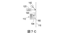
- 前記ホルダは、
プラテンと、
前記部材を受け取り、前記ホルダが前記部材に沿って摺動することを可能にする少なくとも1つのスリーブであって、前記少なくとも1つのスリーブは、前記複数のプリントヘッドおよび前記UV硬化装置に面する前記プラテンの表面の反対側にある前記プラテンの表面に接続されて、前記ホルダの前記プラテンが前記複数のプリントヘッドおよび前記UV硬化装置に対向して通過するようにする少なくとも1つのスリーブと
をさらに含む請求項2に記載の印刷システム。 - 前記部材は、前記プロセス方向に整列され、互いに所定の分離距離だけ離間された上部および下部を有し、前記所定の分離距離は前記少なくとも1つのスリーブの長さよりも小さく、
前記UV硬化装置と前記UV検出器との間に置かれた前記部材の前記上部と前記部材の前記下部が分離された状態で、前記UV硬化装置および前記UV検出器は互いに対向している請求項4に記載の印刷システム。 - 印刷システムの動作方法であって、
UV光をUV光検出器に向けるためにコントローラを備えた紫外線(UV)硬化装置を動作させるステップであって、前記UV硬化装置は複数のUV発光ダイオード(LED)を有し、前記UV検出器は複数のUVセンサを有し、前記UV硬化装置内の各UV LEDはUV光を放射するように構成され、各UVセンサは、前記UV硬化装置内の前記UV LEDの1つからUV光を受け取り、前記UVセンサによって受け取られたUV光の強度に対応する電気信号を生成するように構成される、ステップと、
前記UV検出器内の前記UVセンサによって生成された電気信号を前記コントローラで受信するステップと、
所定の強度以上でUV光を放射していない前記UV硬化装置内のUV LEDを前記コントローラで識別するステップと、
前記コントローラによってアクチュエータを動作させて、前記UV硬化装置内の単一のUV LEDによって放射されるUV光の幅に対応する所定の距離だけ前記UV硬化装置をクロスプロセス方向に移動させるステップと、
前記コントローラによって他のアクチュエータを動作させて、再配置された前記UV硬化装置を通過して物体を移動させ、前記UV硬化装置内の動作可能なUV LEDがUV光を、所定の強度以上のUV光を放射していないと識別されたUV LEDに対向した前記物体の領域に放射するステップと
を含む、方法。 - 所定の強度以上のUV光を放射することができないUV LEDの識別は、
前記UV検出器内の前記UVセンサから受け取った各電気信号の電圧を、前記所定の強度に対応する所定の電圧レベルと比較するステップ
をさらに含む請求項6に記載の方法。
Applications Claiming Priority (2)
| Application Number | Priority Date | Filing Date | Title |
|---|---|---|---|
| US15/610,779 US10052888B1 (en) | 2017-06-01 | 2017-06-01 | System and method for detecting defective ultraviolet radiating light emitting diodes in a printer |
| US15/610,779 | 2017-06-01 |
Publications (3)
| Publication Number | Publication Date |
|---|---|
| JP2018202862A JP2018202862A (ja) | 2018-12-27 |
| JP2018202862A5 JP2018202862A5 (ja) | 2021-07-26 |
| JP6976902B2 true JP6976902B2 (ja) | 2021-12-08 |
Family
ID=63144586
Family Applications (1)
| Application Number | Title | Priority Date | Filing Date |
|---|---|---|---|
| JP2018092654A Active JP6976902B2 (ja) | 2017-06-01 | 2018-05-14 | プリンタ内の欠陥紫外線放射発光ダイオードを検出するシステムおよび方法 |
Country Status (3)
| Country | Link |
|---|---|
| US (2) | US10052888B1 (ja) |
| JP (1) | JP6976902B2 (ja) |
| DE (1) | DE102018113127B4 (ja) |
Families Citing this family (2)
| Publication number | Priority date | Publication date | Assignee | Title |
|---|---|---|---|---|
| US11897171B2 (en) * | 2017-01-13 | 2024-02-13 | Lg Innotek Co., Ltd. | Curing-device |
| JP2022026973A (ja) * | 2020-07-31 | 2022-02-10 | 株式会社リコー | 液体吐出装置及び液体吐出方法 |
Family Cites Families (17)
| Publication number | Priority date | Publication date | Assignee | Title |
|---|---|---|---|---|
| AUPP996099A0 (en) | 1999-04-23 | 1999-05-20 | Silverbrook Research Pty Ltd | A method and apparatus(sprint01) |
| US20040179079A1 (en) | 2002-11-20 | 2004-09-16 | Takeshi Yokoyama | Ink jet printer and ultraviolet ray irradiating device |
| US7264346B2 (en) | 2003-07-15 | 2007-09-04 | Konica Minolta Medical & Graphic, Inc. | Inkjet printer using ultraviolet cure ink |
| JP4649935B2 (ja) | 2004-02-02 | 2011-03-16 | コニカミノルタホールディングス株式会社 | インクジェットプリンタ |
| JP4311216B2 (ja) | 2004-02-02 | 2009-08-12 | コニカミノルタホールディングス株式会社 | インクジェット記録装置 |
| JP4802076B2 (ja) | 2006-09-29 | 2011-10-26 | 富士フイルム株式会社 | 活性エネルギー硬化型インクジェット記録装置 |
| US7794075B2 (en) | 2006-12-25 | 2010-09-14 | Seiko Epson Corporation | Ultraviolet ray irradiation device, recording apparatus using the ultraviolet ray irradiation device, and recording method |
| JP5417902B2 (ja) * | 2009-03-04 | 2014-02-19 | セイコーエプソン株式会社 | 描画装置 |
| US8993983B2 (en) | 2010-05-13 | 2015-03-31 | Nail Alliance Llc | UV LED curing apparatus with improved housing and switch controller |
| JP5812239B2 (ja) * | 2010-12-02 | 2015-11-11 | セイコーエプソン株式会社 | 記録装置 |
| JP5760445B2 (ja) * | 2011-01-17 | 2015-08-12 | セイコーエプソン株式会社 | 印刷方法、印刷装置及び成形印刷物製造方法並びに成形印刷物製造装置 |
| JP5776882B2 (ja) * | 2011-04-11 | 2015-09-09 | セイコーエプソン株式会社 | 記録装置 |
| US8814344B2 (en) | 2012-06-29 | 2014-08-26 | Xerox Corporation | Method and apparatus for monitoring and controlling the performance of an ultraviolet curing station useful in printing |
| WO2014204020A1 (ko) | 2013-06-17 | 2014-12-24 | 한국프린티드일렉트로닉스연구조합 | 자외선 발광 다이오드를 이용한 3d 프린터용 경화 장치 |
| US9073362B2 (en) * | 2013-08-27 | 2015-07-07 | Oce-Technologies B.V. | Inkjet printer assembly using a gelling UV curable ink |
| US10589466B2 (en) * | 2015-02-28 | 2020-03-17 | Xerox Corporation | Systems and methods for implementing multi-layer addressable curing of ultraviolet (UV) light curable inks for three dimensional (3D) printed parts and components |
| JP6004125B1 (ja) * | 2016-01-18 | 2016-10-05 | 富士ゼロックス株式会社 | 液滴乾燥装置、及び画像形成装置 |
-
2017
- 2017-06-01 US US15/610,779 patent/US10052888B1/en active Active
-
2018
- 2018-05-14 JP JP2018092654A patent/JP6976902B2/ja active Active
- 2018-06-01 DE DE102018113127.5A patent/DE102018113127B4/de active Active
- 2018-07-17 US US16/037,312 patent/US10688809B2/en active Active
Also Published As
| Publication number | Publication date |
|---|---|
| US10688809B2 (en) | 2020-06-23 |
| DE102018113127A1 (de) | 2018-12-06 |
| US10052888B1 (en) | 2018-08-21 |
| JP2018202862A (ja) | 2018-12-27 |
| DE102018113127B4 (de) | 2025-07-17 |
| US20180345683A1 (en) | 2018-12-06 |
Similar Documents
| Publication | Publication Date | Title |
|---|---|---|
| JP3987970B2 (ja) | インクジェット記録装置 | |
| JP6976902B2 (ja) | プリンタ内の欠陥紫外線放射発光ダイオードを検出するシステムおよび方法 | |
| JP2015037870A (ja) | 印刷装置及び印刷方法 | |
| EP2759410B1 (en) | Recording apparatus | |
| US11225066B2 (en) | In-line detection and correction of underperforming light emitting diodes in a curing station of a three dimensional object printer | |
| US9688081B1 (en) | Droplet drying device and image forming apparatus | |
| US20150273868A1 (en) | Printing unit and printing apparatus | |
| JP7058130B2 (ja) | 印刷装置 | |
| US10807354B2 (en) | Active light emitting diode ultra violet curing system for a three dimensional object printer | |
| US11491806B2 (en) | Cure confirmation system and method for three dimensional object printer | |
| JP2016068560A5 (ja) | ||
| JP2015196379A5 (ja) | オブジェクト形成するプリンタ及び、プリントヘッド内の不動作インクジェットを検出する装置 | |
| US11198285B2 (en) | Active transparent display for dynamic masking during UV curing in a three dimensional object printer | |
| JP5617588B2 (ja) | 印刷装置及び印刷方法 | |
| US8085288B2 (en) | Exposure system with a plurality of laser sources located at dispersed sites | |
| JP2008100399A (ja) | 発光装置、発光装置の製造方法及びインクジェット記録装置 | |
| US20140210880A1 (en) | Uniform output of light-emitting diode array | |
| JP2018202862A5 (ja) | ||
| KR20200043904A (ko) | 다이렉트-투-오브젝트 프린터에서 자외선 경화성 잉크로 3차원 물체 상에 인쇄하기 위한 시스템 및 방법 | |
| US10467773B2 (en) | In-line failure detection of a curing light source of a three dimensional object printer | |
| US20180250956A1 (en) | Inkjet printer | |
| JP6351297B2 (ja) | プリント装置 | |
| JP2014015054A (ja) | 印刷装置 | |
| KR102390744B1 (ko) | 물체 상에 이미지를 프린트하기 위한 위치를 식별 및 물체 상에 이미지를 프린트하기 위해 프린트 헤드를 작동시키기 위한 시스템 및 방법 | |
| US10434799B2 (en) | Systems and methods for reducing banding artefacts of an image on a substrate |
Legal Events
| Date | Code | Title | Description |
|---|---|---|---|
| RD02 | Notification of acceptance of power of attorney |
Free format text: JAPANESE INTERMEDIATE CODE: A7422 Effective date: 20180523 |
|
| RD04 | Notification of resignation of power of attorney |
Free format text: JAPANESE INTERMEDIATE CODE: A7424 Effective date: 20180814 |
|
| RD03 | Notification of appointment of power of attorney |
Free format text: JAPANESE INTERMEDIATE CODE: A7423 Effective date: 20210311 |
|
| RD04 | Notification of resignation of power of attorney |
Free format text: JAPANESE INTERMEDIATE CODE: A7424 Effective date: 20210415 |
|
| A521 | Request for written amendment filed |
Free format text: JAPANESE INTERMEDIATE CODE: A523 Effective date: 20210512 |
|
| A621 | Written request for application examination |
Free format text: JAPANESE INTERMEDIATE CODE: A621 Effective date: 20210512 |
|
| A871 | Explanation of circumstances concerning accelerated examination |
Free format text: JAPANESE INTERMEDIATE CODE: A871 Effective date: 20210512 |
|
| A131 | Notification of reasons for refusal |
Free format text: JAPANESE INTERMEDIATE CODE: A131 Effective date: 20210701 |
|
| A521 | Request for written amendment filed |
Free format text: JAPANESE INTERMEDIATE CODE: A523 Effective date: 20210927 |
|
| TRDD | Decision of grant or rejection written | ||
| A01 | Written decision to grant a patent or to grant a registration (utility model) |
Free format text: JAPANESE INTERMEDIATE CODE: A01 Effective date: 20211011 |
|
| A61 | First payment of annual fees (during grant procedure) |
Free format text: JAPANESE INTERMEDIATE CODE: A61 Effective date: 20211110 |
|
| R150 | Certificate of patent or registration of utility model |
Ref document number: 6976902 Country of ref document: JP Free format text: JAPANESE INTERMEDIATE CODE: R150 |
|
| R250 | Receipt of annual fees |
Free format text: JAPANESE INTERMEDIATE CODE: R250 |