JP6976902B2 - Systems and Methods for Detecting Defective UV Emitting Light Emitting Diodes in Printers - Google Patents
Systems and Methods for Detecting Defective UV Emitting Light Emitting Diodes in Printers Download PDFInfo
- Publication number
- JP6976902B2 JP6976902B2 JP2018092654A JP2018092654A JP6976902B2 JP 6976902 B2 JP6976902 B2 JP 6976902B2 JP 2018092654 A JP2018092654 A JP 2018092654A JP 2018092654 A JP2018092654 A JP 2018092654A JP 6976902 B2 JP6976902 B2 JP 6976902B2
- Authority
- JP
- Japan
- Prior art keywords
- curing device
- light
- led
- detector
- controller
- Prior art date
- Legal status (The legal status is an assumption and is not a legal conclusion. Google has not performed a legal analysis and makes no representation as to the accuracy of the status listed.)
- Active
Links
- 238000000034 method Methods 0.000 title claims description 45
- 230000002950 deficient Effects 0.000 title description 36
- 238000003848 UV Light-Curing Methods 0.000 claims description 78
- 230000008569 process Effects 0.000 claims description 27
- 238000001723 curing Methods 0.000 claims description 22
- 239000000463 material Substances 0.000 claims description 10
- 238000000926 separation method Methods 0.000 claims 2
- 239000000976 ink Substances 0.000 description 25
- 230000005855 radiation Effects 0.000 description 12
- 230000004044 response Effects 0.000 description 7
- 230000008707 rearrangement Effects 0.000 description 5
- 238000010586 diagram Methods 0.000 description 4
- 238000001514 detection method Methods 0.000 description 3
- 238000004519 manufacturing process Methods 0.000 description 3
- 230000008439 repair process Effects 0.000 description 3
- 238000003491 array Methods 0.000 description 2
- 230000007547 defect Effects 0.000 description 2
- 238000009826 distribution Methods 0.000 description 2
- 230000004048 modification Effects 0.000 description 2
- 238000012986 modification Methods 0.000 description 2
- 239000004065 semiconductor Substances 0.000 description 2
- 230000003595 spectral effect Effects 0.000 description 2
- 230000008033 biological extinction Effects 0.000 description 1
- 230000006872 improvement Effects 0.000 description 1
- 230000003287 optical effect Effects 0.000 description 1
- 238000005192 partition Methods 0.000 description 1
- 238000001228 spectrum Methods 0.000 description 1
- 238000003860 storage Methods 0.000 description 1
Images


Classifications
-
- B—PERFORMING OPERATIONS; TRANSPORTING
- B41—PRINTING; LINING MACHINES; TYPEWRITERS; STAMPS
- B41J—TYPEWRITERS; SELECTIVE PRINTING MECHANISMS, i.e. MECHANISMS PRINTING OTHERWISE THAN FROM A FORME; CORRECTION OF TYPOGRAPHICAL ERRORS
- B41J11/00—Devices or arrangements of selective printing mechanisms, e.g. ink-jet printers or thermal printers, for supporting or handling copy material in sheet or web form
- B41J11/0015—Devices or arrangements of selective printing mechanisms, e.g. ink-jet printers or thermal printers, for supporting or handling copy material in sheet or web form for treating before, during or after printing or for uniform coating or laminating the copy material before or after printing
- B41J11/002—Curing or drying the ink on the copy materials, e.g. by heating or irradiating
- B41J11/0021—Curing or drying the ink on the copy materials, e.g. by heating or irradiating using irradiation
- B41J11/00212—Controlling the irradiation means, e.g. image-based controlling of the irradiation zone or control of the duration or intensity of the irradiation
-
- B—PERFORMING OPERATIONS; TRANSPORTING
- B41—PRINTING; LINING MACHINES; TYPEWRITERS; STAMPS
- B41J—TYPEWRITERS; SELECTIVE PRINTING MECHANISMS, i.e. MECHANISMS PRINTING OTHERWISE THAN FROM A FORME; CORRECTION OF TYPOGRAPHICAL ERRORS
- B41J11/00—Devices or arrangements of selective printing mechanisms, e.g. ink-jet printers or thermal printers, for supporting or handling copy material in sheet or web form
- B41J11/0015—Devices or arrangements of selective printing mechanisms, e.g. ink-jet printers or thermal printers, for supporting or handling copy material in sheet or web form for treating before, during or after printing or for uniform coating or laminating the copy material before or after printing
- B41J11/002—Curing or drying the ink on the copy materials, e.g. by heating or irradiating
- B41J11/0021—Curing or drying the ink on the copy materials, e.g. by heating or irradiating using irradiation
- B41J11/00214—Curing or drying the ink on the copy materials, e.g. by heating or irradiating using irradiation using UV radiation
-
- G—PHYSICS
- G01—MEASURING; TESTING
- G01J—MEASUREMENT OF INTENSITY, VELOCITY, SPECTRAL CONTENT, POLARISATION, PHASE OR PULSE CHARACTERISTICS OF INFRARED, VISIBLE OR ULTRAVIOLET LIGHT; COLORIMETRY; RADIATION PYROMETRY
- G01J1/00—Photometry, e.g. photographic exposure meter
- G01J1/02—Details
- G01J1/04—Optical or mechanical part supplementary adjustable parts
- G01J1/06—Restricting the angle of incident light
-
- G—PHYSICS
- G01—MEASURING; TESTING
- G01J—MEASUREMENT OF INTENSITY, VELOCITY, SPECTRAL CONTENT, POLARISATION, PHASE OR PULSE CHARACTERISTICS OF INFRARED, VISIBLE OR ULTRAVIOLET LIGHT; COLORIMETRY; RADIATION PYROMETRY
- G01J1/00—Photometry, e.g. photographic exposure meter
- G01J1/42—Photometry, e.g. photographic exposure meter using electric radiation detectors
- G01J1/429—Photometry, e.g. photographic exposure meter using electric radiation detectors applied to measurement of ultraviolet light
-
- G—PHYSICS
- G01—MEASURING; TESTING
- G01J—MEASUREMENT OF INTENSITY, VELOCITY, SPECTRAL CONTENT, POLARISATION, PHASE OR PULSE CHARACTERISTICS OF INFRARED, VISIBLE OR ULTRAVIOLET LIGHT; COLORIMETRY; RADIATION PYROMETRY
- G01J1/00—Photometry, e.g. photographic exposure meter
- G01J1/42—Photometry, e.g. photographic exposure meter using electric radiation detectors
- G01J2001/4247—Photometry, e.g. photographic exposure meter using electric radiation detectors for testing lamps or other light sources
- G01J2001/4252—Photometry, e.g. photographic exposure meter using electric radiation detectors for testing lamps or other light sources for testing LED's
Landscapes
- Physics & Mathematics (AREA)
- General Physics & Mathematics (AREA)
- Spectroscopy & Molecular Physics (AREA)
- Health & Medical Sciences (AREA)
- General Health & Medical Sciences (AREA)
- Toxicology (AREA)
- Ink Jet (AREA)
Description
本開示は、一般に、3次元(3D)物体に印刷するシステムに関し、より詳細には、紫外線(UV)硬化型インクを用いて物体に印刷するシステムに関する。 The present disclosure relates generally to systems that print on three-dimensional (3D) objects, and more particularly to systems that print on objects using UV (UV) curable inks.
商業用物品印刷は、通常、物品の製造中に行われる。例えば、ボール表皮には、ボールが完成して膨張される前にパターンまたはロゴが印刷される。その結果、潜在的な製品顧客が複数のプロチームまたは大学チームを支援する地域において、配布サイトまたは小売店などの非製造施設は、地域で人気の様々なチームのロゴを載せる製品の在庫を維持する必要がある。在庫を維持するために、異なるロゴごとに正しい数の製品を注文することは問題になり得る。 Commercial article printing is usually done during the manufacture of the article. For example, the ball skin is printed with a pattern or logo before the ball is completed and inflated. As a result, in areas where potential product customers support multiple professional or university teams, non-manufacturing facilities such as distribution sites or retail stores maintain inventory of products bearing the logos of various teams popular in the area. There is a need to. Ordering the correct number of products for different logos to maintain inventory can be a problem.
非生産店でこれらの問題に対処する1つの方法は、印刷されていないバージョンの製品を保管し、配布サイトや小売店でパターンやロゴを印刷することである。個々の物体を印刷するために、direct−to−object(DTO)プリンタとして知られているプリンタが開発されている。これらのプリンタのいくつかは、UV硬化型インクを使用して、物体上にインク画像を形成する。UV硬化型インクは、物体表面のインク上にUV光を向けるUV放射源を必要とする。この光はインクを硬化させ、さもなければインクから発散する蒸気を除去するのに役立つ。これらの蒸気の中には、人に有害なものがある。 One way to address these issues in non-manufacturing stores is to store unprinted versions of the product and print patterns and logos on distribution sites and retail stores. Printers known as direct-to-object (DTO) printers have been developed for printing individual objects. Some of these printers use UV curable ink to form an ink image on an object. UV curable inks require a UV source that directs UV light onto the ink on the surface of the object. This light cures the ink and otherwise helps remove the vapors emanating from the ink. Some of these vapors are harmful to humans.
UV放射発光ダイオード(LED)は、UV放射源の1つの効率的な形態である。これらの半導体装置は、装置内の半導体接合部に印加されるDC電圧に応答して、光スペクトルのUV範囲内の光を生成する。典型的には、これらのUV LEDは、インク印刷のために1つまたは複数のプリントヘッドを通過するホルダおよび物体の移動経路に対して垂直であるクロスプロセス方向に延在するLEDのアレイ内に配置される。この文書では、「プロセス方向」とは、プリンタにおいてプリントヘッドを通過する物体の移動方向を指し、「クロスプロセス方向」とは、物体のホルダが移動する平面に平行な平面においてプロセス方向に垂直な軸を指す。UV LEDの動作寿命にわたって、LEDのいくつかは、UVインクを硬化させるのに有効な強度を有するUV光をもはや放射しなくなるまで、低いレベルで放射を生成し始める。UVインクの硬化に完全に無効になる前に、プリンタ内のUV LEDのこの消滅を検出することは有益である。 UV light emitting diodes (LEDs) are an efficient form of UV radiation source. These semiconductor devices generate light within the UV range of the optical spectrum in response to a DC voltage applied to the semiconductor junction within the device. Typically, these UV LEDs are in an array of LEDs that extend in a cross-process direction that is perpendicular to the path of movement of the holder and object through one or more printheads for ink printing. Be placed. In this document, "process direction" refers to the direction of movement of an object through the printhead in a printer, and "cross-process direction" is perpendicular to the process direction in a plane parallel to the plane in which the holder of the object moves. Point to the axis. Throughout the operating life of a UV LED, some of the LEDs begin to generate radiation at low levels until they no longer emit UV light that has an intensity effective in curing the UV ink. It is useful to detect this extinction of the UV LED in the printer before it is completely ineffective in curing the UV ink.
新しい印刷システムは、UV硬化型インクを吐出してインク画像を形成するプリンタにおける欠陥UV LEDを識別するように構成された検出器を含む。印刷システムは、複数のプリントヘッドであって、複数のプリントヘッド内の各プリントヘッドがマーキング材料を吐出するように構成されるプリントヘッドと、複数のUV発光ダイオード(LED)を有する紫外線(UV)硬化装置であって、UV硬化装置内の各UV LEDはUV光を放射するように構成され、UV硬化装置はプリントヘッドの少なくとも1つが表面上にUVマーキング材料を吐出した後にUVマーキング材料を硬化させるように配置される、紫外線硬化装置と、複数のUVセンサを有するUV検出器であって、各UVセンサは、UV検出器内のUV LEDの1つからUV光を受け取り、UVセンサによって受け取られたUV光の強度に対応する電気信号を生成するように構成される、UV検出器と、複数のプリントヘッド、UV硬化装置およびUV検出器に動作可能に接続されたコントローラとを含む。コントローラは、UV硬化装置を動作させて、UV光をUV検出器に向け、UV検出器内のUVセンサによって生成された電気信号を受信し、所定の強度以上のUV光を放射していないUV硬化装置内のUV LEDを識別するように構成される。 The new printing system includes a detector configured to identify defective UV LEDs in printers that eject UV curable ink to form ink images. A printing system is a plurality of printheads, the ultraviolet (UV) having a printhead configured such that each printhead in the plurality of printheads ejects marking material and a plurality of UV light emitting diodes (LEDs). A curing device, each UV LED in the UV curing device is configured to emit UV light, which cures the UV marking material after at least one of the printheads ejects the UV marking material onto the surface. A UV detector with a UV curing device and multiple UV sensors arranged so that each UV sensor receives UV light from one of the UV LEDs in the UV detector and is received by the UV sensor. It includes a UV detector configured to generate an electrical signal corresponding to the intensity of the UV light, and a controller operably connected to multiple printheads, UV curing devices and UV detectors. The controller operates a UV curing device to direct UV light toward the UV detector, receive the electrical signal generated by the UV sensor in the UV detector, and emit UV light of a predetermined intensity or higher. It is configured to identify UV LEDs in the curing device.
欠陥UV LEDを識別するように構成された検出器を有するプリンタを操作する方法は、画像がプリンタを出る前にUV硬化インク画像が適切に硬化されることを保証するのに役立つ。この方法は、UV光をUV光検出器に向けるためにコントローラを備えた紫外線(UV)硬化装置を動作させるステップであって、UV硬化装置は複数のUV発光ダイオード(LED)を有し、UV検出器は複数のUVセンサを有し、UV硬化装置内の各UV LEDはUV光を放射するように構成され、各UVセンサは、UV硬化装置内のUV LEDの1つからUV光を受け取り、UVセンサによって受け取られたUV光の強度に対応する電気信号を生成するように構成される、ステップと、UV検出器内のUVセンサによって生成された電気信号をコントローラで受信するステップと、所定の強度以上でUV光を放射していないUV硬化装置内のUV LEDをコントローラで識別するステップを含む。 A method of operating a printer with a detector configured to identify defective UV LEDs helps ensure that the UV curable ink image is properly cured before the image leaves the printer. This method is a step of operating an ultraviolet (UV) curing device equipped with a controller to direct UV light to a UV light detector, the UV curing device having multiple UV emitting diodes (LEDs) and UV. The detector has multiple UV sensors, each UV LED in the UV curing device is configured to emit UV light, and each UV sensor receives UV light from one of the UV LEDs in the UV curing device. , A step configured to generate an electrical signal corresponding to the intensity of the UV light received by the UV sensor, and a step of receiving the electrical signal generated by the UV sensor in the UV detector on the controller. Includes a step of identifying the UV LED in the UV curing device with a controller that does not emit UV light above the intensity of.
プリンタ内の欠陥UV LEDを識別する印刷システムの前述の態様および他の特徴は、添付図面と関連して以下の説明において説明される。 The aforementioned aspects and other features of a printing system that identifies defective UV LEDs in a printer are described in the following description in connection with the accompanying drawings.
本実施形態の一般的な理解のために、図面を参照する。図面において、同様の参照番号は同様の要素を示すために全体を通して使用されている。 Refer to the drawings for a general understanding of this embodiment. In the drawings, similar reference numbers are used throughout to indicate similar elements.
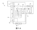
図1は、ホルダ108がプリントヘッド118のアレイを通過した部材116上の矢印によって示されるプロセス方向に移動するときに、ホルダ108に取り付けられた物体104の表面を印刷するように構成された印刷システム100を示す。アレイ112内の1つまたは複数のプリントヘッド118が紫外線(UV)インクを吐出する場合、UV硬化装置120はコントローラ124によって動作されUVインクを硬化させる。コントローラ124はまた、物体がホルダに取り付けられた後に、アクチュエータ128を動作させて、ホルダ108を部材116に沿って移動させるように構成される。コントローラ124は、アレイ112内のプリントヘッド118を動作させ、マーキング材料を物体104の表面に吐出させるように構成される。電気スイッチ130は、電源134とUV硬化装置120との間に動作可能に接続されている。コントローラ124はスイッチ130に動作可能に接続され、電源134をUV硬化装置120に選択的に結合する。コントローラ124は、アクチュエータ138を動作させ、以下に詳述するように、UV硬化装置120をホルダ108のプロセス方向に直交するクロスプロセス方向に移動させる。物体104またはホルダ108が検出器142とUV硬化装置120との間に置かれていない場合、UV検出器142は装置120に対向して配置され、装置120からUV放射を受け取る。本明細書で使用される場合、「UV光」は、可視光よりも短いがX線よりも長い波長を有する光を指す。この範囲の光は約10〜400nmの波長を有する。
FIG. 1 is a print configured to print the surface of an
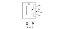
従来技術で知られているホルダ108の一実施形態が図1Bに示されている。ホルダ108は、部材116を受け取る一対のスリーブ132およびプラテン136を含む。この構成は、ホルダ108のプラテン136を部材116からオフセットする。プリントヘッド118は部材116の長手方向軸からクロスプロセス方向にオフセットされて、プリントヘッドがホルダ108に保持された物体に向けてインクを吐出することを可能にする。同様に、UV硬化装置120とUV検出器142はクロスプロセス方向にオフセットされ、UV硬化装置がUV光を物体104上のインク画像の方に向け、物体上のUV硬化型インクを硬化させる。UV検出器はまた、UV硬化装置とは反対のプロセス方向にオフセットされているので、以下でより詳細に説明するように、ホルダ108がUV硬化装置とUV検出器との間に置かれていない場合、UV硬化装置のUVセンサからUV光を受けることができる。
An embodiment of the
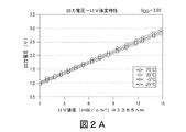
図2Aは、センサが受け取るUV光の強度に関して、UV検出器142内のUVセンサの出力電圧レベルを示すグラフである。UV放射強度が増加すると、UVセンサの出力電圧は線形的に増加する。この関係は、図に示される温度のそれぞれについてほぼ同じである。図2Bは、同じセンサの分光応答度を示すグラフである。
FIG. 2A is a graph showing the output voltage level of the UV sensor in the
図3は、UV硬化装置120内のUV LEDアレイの構造と、UV硬化装置内の欠陥UV LEDを識別するためのUV検出器142の構造を示すブロック図である。硬化装置120は、ハウジング304とUV LEDアレイ308A〜308Eとを含む。LED308A〜308Eは入力電圧接続部312および戻り接続部316に電気的に接続され、硬化装置120のUV LEDを電源134に結合することができる。入力電圧接続部312は、スイッチ130を介して電圧供給部134の出力に接続され、スイッチは、コントローラ124によって動作され、電圧供給部134を硬化装置120内のLEDに選択的に結合する。図は5つのLED308A〜308Eを示しているが、LEDの数は、ホルダ108が収容できる最も広い物体の幅に対応する距離に対して、クロスプロセス方向にホルダ108の経路にわたって延びるUV放射の連続線をLEDが形成することを可能にする数である。
FIG. 3 is a block diagram showing the structure of the UV LED array in the
引き続き図3を参照すると、UV検出器142は、UV LED308A〜308Eと1対1に対応して、UVセンサ324A〜324Eのアレイがクロスプロセス方向に配列されたハウジング320を含む。隣接するUVセンサの間には、剛性仕切り328がある。これらの仕切りは、特定のUVセンサの正反対ではないUV LEDによって生成されるUV放射から各UVセンサを遮蔽するのに役立つ。この構成は、各UVセンサが、UVセンサの正反対にある硬化装置120のUV LEDに対応することを保証するのに役立つ。UV硬化装置120のUV LED308A〜308Eが動作され、UV光をUV検出器142のUVセンサ324A〜324Eにそれぞれ向けながら、UVセンサ324A〜324Eの出力はコントローラ124に出力され、コントローラが出力信号を参照して欠陥UV LEDを識別するのを可能にする。コントローラ124は、これらの信号を所定の閾値と比較して、LEDのいずれかが欠陥であると識別するか否かを決定する。一実施形態では、UVセンサは、コロラド州NiwotのSparkFun Electronicsによって製造された部品番号ML8511であるが、他の適切なUVセンサを使用することもできる。ユーザインターフェース340は、コントローラ124に動作可能に接続され、以下により詳細に説明するように、コントローラがUV硬化装置120の修理のための表示を生成することを可能にする。
Continuing with reference to FIG. 3, the
図4は、LEDアレイ308A〜308Eにおける欠陥UV LEDと、UV検出器におけるUVセンサ324A〜324Eの応答を示すブロック図である。図に示すように、硬化装置120のUV LED308Bは、そのLEDから進行する矢印の不在によって示されるようにUV光を生成しない。その結果、UV LED308Bに対向するUVセンサ324Bは、物体上のUVインクを硬化させるのに適した最小UV強度に対応する閾値250未満の出力電圧レベルを生成する。残りのUV LED308Aおよび308C〜308Eは、残りのUVセンサによって生成された出力電圧が閾値を上回る十分な量のUV放射を生成する。したがって、コントローラ124は、UV硬化装置120内のUV LED308Bが、装置120内の唯一の欠陥LEDであると特定する。
FIG. 4 is a block diagram showing the responses of the defective UV LEDs in the
UV検出器142内のUVセンサ324A〜324Eによって生成された信号から、コントローラ124によって欠陥UV LEDが検出されると、欠陥LEDを交換せずにプリンタ100が動作を継続できるようにするために、UV硬化装置120の配置に対する調整を行うことができる。図5は、欠陥UV LEDの検出に対処するUV硬化動作のそのような調整を示す。図では、UV LED故障の10個の異なるシナリオ504、508、512、516、520、524、528、532、536、および540が示されている。シナリオ504において、UV LEDは、上で使用された参照番号、すなわち308A〜308Eによって識別される。これらの参照番号は、図5に示す他のシナリオのUV LEDにも当てはまる。シナリオ504では、UV LED308Aが欠陥品であると識別される。この状況に対処するために、コントローラ124は、アクチュエータ128を動作させて、ホルダ108および物体104を1回目の通過でUV硬化装置120を通過させ、UV LED308B〜308EがUVインクを硬化できるようにする。次に、コントローラ124はアクチュエータ138を動作させて、UV硬化装置120を1つのUV LED放射パターンの幅だけクロスプロセス方向に左に移動させた後、アクチュエータ128を動作させて、再配置された硬化装置120によって生成されたUV放射線を通って、ホルダ108および物体104を移動させる。この再配置により、LED308Bは、欠陥LED308Aを交換し、硬化装置による2回目の通過中にUVインクを照射することができる。シナリオ508、512、516、および520は、1つのUV LEDのみが欠陥として識別されるシナリオである。これらのシナリオのそれぞれにおいて、コントローラ124は、シナリオ504を参照して説明したのと同様の方法でアクチュエータ128および138を動作させて、UV硬化装置120によってホルダ108および物体104を2回通過させ、2つの通過の間に1つのUV LED放射パターンの幅に対応する距離だけUV硬化装置を再配置させ、物体104上の未硬化領域を装置120内の動作可能なUV LEDによって硬化させることができる。他の可能性のある再配置動作は、同じ目的を達成することができる。
When a defective UV LED is detected by the
シナリオ524、528、532、536、および540では、硬化装置120の2つのLEDが欠陥品であると識別されている。再び、欠陥LEDの検出に応答して、コントローラ124は、シナリオ504を参照して説明したのと同様の方法でアクチュエータ128および138を動作させて、UV硬化装置120によってホルダ108および物体104を2回通過させ、2回の通過の間に1つのUV LED放射パターンの幅に対応する距離だけUV硬化装置を再配置させ、物体104上の両方の未硬化領域を装置120内の2つの動作可能なUV LEDによって硬化させることができる。他の可能性のある再配置動作は、同じ目的を達成することができる。
In
2回以上の通過と組み合わせた硬化装置120の複数の再配置が、他の欠陥LEDシナリオに対処するために使用され得るが、それらは実施するにはあまりにも非効率的であると考えられる。例えば、LED308AおよびLED308Eの両方が欠陥品であると識別された場合、矯正の解決策は、硬化装置の再配置のために3回の通過および2回のクロスプロセス方向の移動を必要とする。このようなシナリオでは、1つの再配置によって、装置120を右または左方向のいずれかに1つの放射パターンの距離だけ移動させて、欠陥のある右端または左端の欠陥LEDにより未硬化領域をそれぞれ硬化させる。残りの未硬化領域に対処するために、硬化装置は、2つの放射パターン幅に対応する距離だけクロスプロセス軸に沿って反対方向に移動される。これらの複数回の通過および再配置動作は時間を消費し、物体上の画像の印刷および硬化を非効率的にする可能性がある。代わりに、コントローラ124は、プリンタが動作状態に戻る前に、UV硬化装置120が欠陥LEDを交換する修理を必要とするという指示を生成するために、ユーザインターフェース340に信号を生成することができる。
Multiple rearrangements of the
プリンタ100を動作させるプロセスを図6に示す。プロセスの説明において、プロセスが何らかのタスクまたは機能を実行しているという記述は、コントローラまたはプロセッサに動作可能に接続された非一時的コンピュータ可読記憶媒体に格納されたプログラム命令を実行して、データを操作するか、タスクまたは機能を実行するためにプリンタ内の1つまたは複数の部品を動作するコントローラまたは汎用プロセッサを指す。上述したコントローラ124は、そのようなコントローラまたはプロセッサとすることができる。あるいは、コントローラは、複数のプロセッサならびに関連する回路および部品で実装することができ、各々は、本明細書で説明する1つまたは複数のタスクまたは機能を形成するように構成される。さらに、この方法のステップは、図に示される順序または処理が記述される順序にかかわらず、任意の実行可能な時間順に実行されてもよい。
The process of operating the
図6は、図5に示す調整動作を実施するプロセスのフロー図である。このプロセスは、装置がUV検出器142内のUVセンサ308と1対1に対応して位置合わせされている間に、UV硬化装置120を動作させることによって開始される(ブロック604)。コントローラ124は、各UVセンサからの出力信号を比較して、UVセンサの全てが動作しているか否かを判定する(ブロック608)。それらが全て動作している場合、物体は印刷され、UV硬化装置による一回の通過は物体に印刷されたUVインクを硬化させるのに十分である(ブロック612)。1つまたは複数の欠陥LEDが検出された場合、プロセスは欠陥UV LEDを識別し(ブロック616)、欠陥パターンが2回通過解決策で対処可能であるか否かを判定する(ブロック620)。可能であれば、2回の通過の間で適切な再配置が実行され、2回通過の物体印刷を実施する(ブロック624)。そうでなければ、コントローラは、UV硬化装置が欠陥LEDを交換するために修理を必要とすることを示す表示を生成する(ブロック628)。1回通過または2回通過のいずれかの物体印刷によって物体が印刷されると、プロセスは別の物体が印刷されるか否かを決定し(ブロック632)、別の物体が印刷準備ができている場合、印刷前にUV LEDがチェックされる(ブロック604および608)。そうでなければ、プロセスは、別の物体が印刷準備ができるまで待つ。
FIG. 6 is a flow chart of a process for carrying out the adjustment operation shown in FIG. This process is initiated by operating the
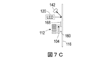
硬化装置内のUV LEDがUV検出器内のUVセンサを照射することを可能にするために、構成要素を異なるように構成するプリンタ100の異なる実施形態が示されている。図7Aにおいて、ホルダ108は、部材116を受け取る単一のスリーブ160を有する。スリーブ160は、部材116の端部116Aと端部116Bとの間のギャップ距離より大きい長さを有する。この構成は、プリントヘッドアレイ112を、上述したように部材からオフセットするのではなく、部材116に対向して配置することを可能にする。ギャップ距離により、スリーブ160は上部116Cに続き、UV硬化装置120はUV光を物体104に向けることができる。図7Bでは、部材116は連続的であるが、プリントヘッドアレイ112はオフセットされているのではなく、部材116に対向している。UV検出器142は、スリーブ160から伸びている。この構成は、物体がUV硬化装置を通過する前に、UV検出器がUV硬化装置120に対向して通過することを可能にする。このように、UV硬化装置は光をUV検出器に向け、UV検出器のUVセンサがコントローラ124によって処理される信号を生成するので、コントローラは任意の欠陥LEDを識別して、物体上のインク画像を硬化させるために1回通過または2回通過印刷プロセスを行うことができるか否か判定できる。図7Cでは、部材116は連続的であるが、再び、プリントヘッドアレイ112はオフセットされているのではなく、部材116に対向している。さらに、UV検出器142は、部材116に対して角度をなして配置される。反射面を有する部材168がスリーブ160から延びている。この反射面は、UV硬化装置によって放射されたUV光がUV検出器に反射することを可能にする角度で傾斜している。再び、この部材168およびその反射面により、欠陥UV LEDを識別し、物体がUV硬化装置を通過する前に、1回または2回通過物体印刷プロセスの実現可能性を評価することができる。図7Dでは、部材116は連続的であるが、再び、プリントヘッドアレイ112はオフセットされているのではなく、部材116に対向している。この実施形態では、アクチュエータ138(図1)は、UV硬化装置を回転させ、部材116のUV硬化装置120と同じ側に配置されたUV検出器142に面するようにさらに構成される。コントローラ124がアクチュエータ138を動作させてUV硬化装置120を回転させると、UV硬化装置はUV検出器に面し、任意の欠陥LEDを識別し、1回または2回通過印刷プロセスの実行可能性を評価することができる。物体印刷が可能である場合、コントローラ124はアクチュエータ138を動作させて、UV硬化装置を元の位置に戻して、物体の表面上のUVインクの硬化を可能にする。
Different embodiments of the
上に開示された装置ならびに他の特徴および機能の変形、またはそれらの代替物は、望ましくは多くの他の異なるシステムまたは応用に組み合わされることが理解されよう。例えば、上に開示された欠陥UV LED検出器は、DTOプリンタで使用されると説明されているが、検出器はまた、UV硬化型インクを印刷媒体上に吐出して媒体上に画像を形成し、次にそれらを硬化させる印刷システムで使用できる。当業者であれば、以下の特許請求の範囲に包含されることが意図されているが、今は予期せぬ、または予想せぬ様々な代替、改変、変形または改良を後で実行でき、それらも以下の請求項に包含されることが意図される。
It will be appreciated that the devices and other features and functional variants disclosed above, or their alternatives, are preferably combined with many other different systems or applications. For example, the defective UV LED detector disclosed above is described as being used in a DTO printer, but the detector also ejects UV curable ink onto a print medium to form an image on the medium. And then can be used in printing systems that cure them. Those skilled in the art are intended to be covered by the following claims, but now they can later make various unexpected or unexpected alternatives, modifications, modifications or improvements. Is also intended to be included in the following claims.
Claims (7)
複数のUV発光ダイオード(LED)を有する紫外線(UV)硬化装置であって、前記UV硬化装置内の各UV LEDはUV光を放射するように構成され、前記UV硬化装置は、前記プリントヘッドの少なくとも1つが前記物体の表面上にUVマーキング材料を吐出し、前記物体が前記プロセス方向において前記複数のプリントヘッドを通過して前記UV硬化装置に対向する位置に続いた後に、前記UV硬化装置が前記物体上に吐出されたUVマーキング材料を硬化させる場所で、前記プロセス方向において固定して配置される、紫外線硬化装置と、
複数のUVセンサを有するUV検出器であって、各UVセンサは、前記UV硬化装置内の前記UV LEDの1つからUV光を受け取り、前記UVセンサによって受け取られた前記UV光の強度に対応する電気信号を生成するように構成される、UV検出器と、
前記UV硬化装置に動作可能に接続された第1のアクチュエータと、
前記複数のプリントヘッド、前記UV硬化装置、前記第1のアクチュエータ、および前記UV検出器に動作可能に接続されたコントローラであって、前記コントローラは、前記UV硬化装置を動作させて、UV光を前記UV検出器に向け、前記UV検出器内のUVセンサによって生成された前記電気信号を受信し、所定の強度以上のUV光を放射していない前記UV硬化装置内のUV LEDを識別し、前記第1のアクチュエータを動作させて、前記UV硬化装置内の単一のUV LEDによって放射されるUV光の幅だけ前記UV硬化装置をクロスプロセス方向に再配置し、そして、他のアクチュエータを動作させて、再配置された前記UV硬化装置によって放射される前記UV光を通じて前記物体を通過させ、前記UV硬化装置内の動作可能なUV LEDがUV光を、所定の強度以上のUV光を放射していないと識別されたUV LEDに対向した前記物体の領域に放射するようにする、前記コントローラと
を含む印刷システム。 A plurality of printheads, which are fixedly arranged so as to face the path of movement of an object passing through the plurality of printheads in the process direction, and the object when the object passes through the printhead in the process direction. A printhead configured such that each printhead in the plurality of printheads ejects marking material toward
An ultraviolet (UV) curing device having a plurality of UV light emitting diodes (LEDs), each UV LED in the UV curing device is configured to emit UV light, and the UV curing device is a printhead. After at least one ejects the UV marking material onto the surface of the object and the object continues through the plurality of printheads in the process direction to a position facing the UV curing device, the UV curing device. An ultraviolet curing device fixedly arranged in the process direction at a place where the UV marking material discharged onto the object is cured.
A UV detector with a plurality of UV sensors, each UV sensor receiving UV light from one of the UV LEDs in the UV curing device and corresponding to the intensity of the UV light received by the UV sensor. With a UV detector, which is configured to generate an electrical signal to
A first actuator operably connected to the UV curing device,
A controller operably connected to the plurality of printheads, the UV curing device, the first actuator, and the UV detector, the controller operating the UV curing device to emit UV light. Toward the UV detector, the UV LED in the UV curing device that receives the electrical signal generated by the UV sensor in the UV detector and does not emit UV light of a predetermined intensity or higher is identified. The first actuator is operated to rearrange the UV curing device in the cross-process direction by the width of the UV light emitted by a single UV LED in the UV curing device, and the other actuators are operated. Then, the object is passed through the UV light emitted by the rearranged UV curing device, and the operable UV LED in the UV curing device emits UV light and UV light having a predetermined intensity or higher. A printing system comprising said controller to radiate into the area of said object facing the UV LED identified as not.
物体を保持し、前記部材に沿って前記部材の前記第1の端部と前記第2の端部との間で移動するように構成されたホルダと、
第2のアクチュエータであって、前記第2のアクチュエータが前記ホルダを前記部材に沿って移動させ、前記物体を前記プリントヘッドを通過して移動させて、前記複数のプリントヘッドの前記プリントヘッドからマーキング材料を受け取ることを可能にする、第2のアクチュエータと、
前記UV硬化装置であって、前記複数のプリントヘッドと前記部材の前記第2の端部との間に前記プロセス方向において固定して配置されて、前記UV硬化装置が、前記プロセス方向に移動している前記物体が前記複数のプリントヘッドを通過した後に前記物体上に吐出されるUVマーキング材料を硬化させるようにする、前記UV硬化装置と、
前記コントローラであって、前記第2のアクチュエータに動作可能に接続され、前記第2のアクチュエータを動作させて、前記ホルダおよび前記物体を前記部材に沿ってプロセス方向に移動させて、前記プロセス方向に移動している前記物体が前記複数のプリントヘッド内の前記プリントヘッドを前記UV硬化装置に対向する前記位置まで通過する際に、前記複数のプリントヘッドがマーキング材料を前記物体上に吐出するようにさらに構成される、前記コントローラと
を含む請求項1に記載の印刷システム。 A member having a first end and a second end, wherein the plurality of printheads are fixedly arranged between the first end and the second end of the member. And the members
A holder configured to hold an object and move along the member between the first end and the second end of the member.
A second actuator, the second actuator moving the holder along the member, moving the object through the printhead, and marking from the printhead of the plurality of printheads. A second actuator that allows the material to be received,
The UV curing device is fixedly arranged in the process direction between the plurality of print heads and the second end portion of the member, and the UV curing device moves in the process direction. The UV curing device, which cures the UV marking material ejected onto the object after the object has passed through the plurality of printheads.
The controller, which is operably connected to the second actuator, operates the second actuator to move the holder and the object in the process direction along the member and in the process direction. As the moving object passes the printhead in the plurality of printheads to the position facing the UV curing device, the plurality of printheads eject the marking material onto the object. The printing system according to claim 1, further comprising the controller.
プラテンと、
前記部材を受け取り、前記ホルダが前記部材に沿って摺動することを可能にする少なくとも1つのスリーブであって、前記少なくとも1つのスリーブは、前記複数のプリントヘッドおよび前記UV硬化装置に面する前記プラテンの表面の反対側にある前記プラテンの表面に接続されて、前記ホルダの前記プラテンが前記複数のプリントヘッドおよび前記UV硬化装置に対向して通過するようにする少なくとも1つのスリーブと
をさらに含む請求項2に記載の印刷システム。 The holder is
Platen and
At least one sleeve that receives the member and allows the holder to slide along the member, wherein the at least one sleeve faces the plurality of printheads and the UV curing device. It is connected to the surface of the platen opposite the surface of the platen, further and at least one sleeve the platen before Symbol holder to pass through to face the plurality of print head and the UV curing device The printing system according to claim 2, which includes.
前記UV硬化装置と前記UV検出器との間に置かれた前記部材の前記上部と前記部材の前記下部が分離された状態で、前記UV硬化装置および前記UV検出器は互いに対向している請求項4に記載の印刷システム。 The members are aligned in the process direction and have an upper part and a lower part separated from each other by a predetermined separation distance, the predetermined separation distance being smaller than the length of the at least one sleeve.
A claim that the UV curing device and the UV detector face each other in a state where the upper portion of the member and the lower portion of the member placed between the UV curing device and the UV detector are separated from each other. Item 4. The printing system according to item 4.
UV光をUV光検出器に向けるためにコントローラを備えた紫外線(UV)硬化装置を動作させるステップであって、前記UV硬化装置は複数のUV発光ダイオード(LED)を有し、前記UV検出器は複数のUVセンサを有し、前記UV硬化装置内の各UV LEDはUV光を放射するように構成され、各UVセンサは、前記UV硬化装置内の前記UV LEDの1つからUV光を受け取り、前記UVセンサによって受け取られたUV光の強度に対応する電気信号を生成するように構成される、ステップと、
前記UV検出器内の前記UVセンサによって生成された電気信号を前記コントローラで受信するステップと、
所定の強度以上でUV光を放射していない前記UV硬化装置内のUV LEDを前記コントローラで識別するステップと、
前記コントローラによってアクチュエータを動作させて、前記UV硬化装置内の単一のUV LEDによって放射されるUV光の幅に対応する所定の距離だけ前記UV硬化装置をクロスプロセス方向に移動させるステップと、
前記コントローラによって他のアクチュエータを動作させて、再配置された前記UV硬化装置を通過して物体を移動させ、前記UV硬化装置内の動作可能なUV LEDがUV光を、所定の強度以上のUV光を放射していないと識別されたUV LEDに対向した前記物体の領域に放射するステップと
を含む、方法。 How the printing system works
A step of operating an ultraviolet (UV) curing device equipped with a controller to direct UV light to a UV light detector, wherein the UV curing device has a plurality of UV emitting diodes (LEDs) and the UV detector. Has a plurality of UV sensors, each UV LED in the UV curing device is configured to emit UV light, and each UV sensor emits UV light from one of the UV LEDs in the UV curing device. A step and a step configured to receive and generate an electrical signal corresponding to the intensity of the UV light received by the UV sensor.
The step of receiving the electric signal generated by the UV sensor in the UV detector by the controller, and
A step of identifying a UV LED in the UV curing device that does not emit UV light at a predetermined intensity or higher by the controller, and a step of identifying the UV LED.
A step of operating the actuator by the controller to move the UV curing device in the cross-process direction by a predetermined distance corresponding to the width of the UV light emitted by a single UV LED in the UV curing device.
The controller operates another actuator to move the object through the rearranged UV curing device, and the operable UV LED in the UV curing device emits UV light with UV light of a predetermined intensity or higher. A method comprising radiating into an area of said object facing a UV LED identified as not emitting light.
前記UV検出器内の前記UVセンサから受け取った各電気信号の電圧を、前記所定の強度に対応する所定の電圧レベルと比較するステップ
をさらに含む請求項6に記載の方法。 The identification of UV LEDs that cannot emit UV light above a given intensity is
The method of claim 6, further comprising a step of comparing the voltage of each electrical signal received from the UV sensor in the UV detector with a predetermined voltage level corresponding to the predetermined intensity.
Applications Claiming Priority (2)
| Application Number | Priority Date | Filing Date | Title |
|---|---|---|---|
| US15/610,779 | 2017-06-01 | ||
| US15/610,779 US10052888B1 (en) | 2017-06-01 | 2017-06-01 | System and method for detecting defective ultraviolet radiating light emitting diodes in a printer |
Publications (3)
| Publication Number | Publication Date |
|---|---|
| JP2018202862A JP2018202862A (en) | 2018-12-27 |
| JP2018202862A5 JP2018202862A5 (en) | 2021-07-26 |
| JP6976902B2 true JP6976902B2 (en) | 2021-12-08 |
Family
ID=63144586
Family Applications (1)
| Application Number | Title | Priority Date | Filing Date |
|---|---|---|---|
| JP2018092654A Active JP6976902B2 (en) | 2017-06-01 | 2018-05-14 | Systems and Methods for Detecting Defective UV Emitting Light Emitting Diodes in Printers |
Country Status (3)
| Country | Link |
|---|---|
| US (2) | US10052888B1 (en) |
| JP (1) | JP6976902B2 (en) |
| DE (1) | DE102018113127A1 (en) |
Families Citing this family (2)
| Publication number | Priority date | Publication date | Assignee | Title |
|---|---|---|---|---|
| WO2018131948A1 (en) * | 2017-01-13 | 2018-07-19 | 엘지이노텍 주식회사 | Curing-device |
| JP2022026973A (en) | 2020-07-31 | 2022-02-10 | 株式会社リコー | Liquid discharge device and liquid discharge method |
Family Cites Families (17)
| Publication number | Priority date | Publication date | Assignee | Title |
|---|---|---|---|---|
| AUPP996099A0 (en) | 1999-04-23 | 1999-05-20 | Silverbrook Research Pty Ltd | A method and apparatus(sprint01) |
| US20040179079A1 (en) | 2002-11-20 | 2004-09-16 | Takeshi Yokoyama | Ink jet printer and ultraviolet ray irradiating device |
| EP1498274B1 (en) | 2003-07-15 | 2006-04-05 | Konica Minolta Medical & Graphic Inc. | Inkjet printer using ultraviolet cure ink |
| JP4649935B2 (en) | 2004-02-02 | 2011-03-16 | コニカミノルタホールディングス株式会社 | Inkjet printer |
| JP4311216B2 (en) | 2004-02-02 | 2009-08-12 | コニカミノルタホールディングス株式会社 | Inkjet recording device |
| JP4802076B2 (en) | 2006-09-29 | 2011-10-26 | 富士フイルム株式会社 | Active energy curable ink jet recording apparatus |
| US7794075B2 (en) | 2006-12-25 | 2010-09-14 | Seiko Epson Corporation | Ultraviolet ray irradiation device, recording apparatus using the ultraviolet ray irradiation device, and recording method |
| JP5417902B2 (en) * | 2009-03-04 | 2014-02-19 | セイコーエプソン株式会社 | Drawing device |
| US8993983B2 (en) | 2010-05-13 | 2015-03-31 | Nail Alliance Llc | UV LED curing apparatus with improved housing and switch controller |
| JP5812239B2 (en) * | 2010-12-02 | 2015-11-11 | セイコーエプソン株式会社 | Recording device |
| JP5760445B2 (en) * | 2011-01-17 | 2015-08-12 | セイコーエプソン株式会社 | Printing method, printing apparatus, molded printed material manufacturing method, and molded printed material manufacturing apparatus |
| JP5776882B2 (en) * | 2011-04-11 | 2015-09-09 | セイコーエプソン株式会社 | Recording device |
| US8814344B2 (en) | 2012-06-29 | 2014-08-26 | Xerox Corporation | Method and apparatus for monitoring and controlling the performance of an ultraviolet curing station useful in printing |
| US20160144570A1 (en) | 2013-06-17 | 2016-05-26 | Biomedical 3D Printing Co., Ltd. | Curing Apparatus for 3D Printer, Using Ultraviolet Light Emitting Diode |
| US9073362B2 (en) * | 2013-08-27 | 2015-07-07 | Oce-Technologies B.V. | Inkjet printer assembly using a gelling UV curable ink |
| US10589466B2 (en) * | 2015-02-28 | 2020-03-17 | Xerox Corporation | Systems and methods for implementing multi-layer addressable curing of ultraviolet (UV) light curable inks for three dimensional (3D) printed parts and components |
| JP6004125B1 (en) * | 2016-01-18 | 2016-10-05 | 富士ゼロックス株式会社 | Droplet drying apparatus and image forming apparatus |
-
2017
- 2017-06-01 US US15/610,779 patent/US10052888B1/en active Active
-
2018
- 2018-05-14 JP JP2018092654A patent/JP6976902B2/en active Active
- 2018-06-01 DE DE102018113127.5A patent/DE102018113127A1/en active Pending
- 2018-07-17 US US16/037,312 patent/US10688809B2/en active Active
Also Published As
| Publication number | Publication date |
|---|---|
| JP2018202862A (en) | 2018-12-27 |
| DE102018113127A1 (en) | 2018-12-06 |
| US20180345683A1 (en) | 2018-12-06 |
| US10052888B1 (en) | 2018-08-21 |
| US10688809B2 (en) | 2020-06-23 |
Similar Documents
| Publication | Publication Date | Title |
|---|---|---|
| JP6976902B2 (en) | Systems and Methods for Detecting Defective UV Emitting Light Emitting Diodes in Printers | |
| JP6313149B2 (en) | Printing apparatus and printing method | |
| JP4238907B2 (en) | Inkjet recording device | |
| US9688081B1 (en) | Droplet drying device and image forming apparatus | |
| JP2011083915A (en) | Printing apparatus | |
| US11225066B2 (en) | In-line detection and correction of underperforming light emitting diodes in a curing station of a three dimensional object printer | |
| US9440459B1 (en) | System and method for treating surface of media with a digitally addressable dryer array to reduce moisture gradient and media cockle | |
| US10807354B2 (en) | Active light emitting diode ultra violet curing system for a three dimensional object printer | |
| US20150273868A1 (en) | Printing unit and printing apparatus | |
| US20140210920A1 (en) | Recording apparatus | |
| JP6221848B2 (en) | Drying apparatus, drying program, and image forming apparatus | |
| JP7058130B2 (en) | Printing equipment | |
| JP2016068560A5 (en) | ||
| JP2015196379A5 (en) | Printer for forming object and apparatus for detecting non-operating ink jet in print head | |
| JP5617588B2 (en) | Printing apparatus and printing method | |
| JP2007290399A (en) | Inkjet recording device | |
| US11198285B2 (en) | Active transparent display for dynamic masking during UV curing in a three dimensional object printer | |
| JP2018202862A5 (en) | ||
| KR20200043904A (en) | System and method for printing on three-dimensional objects with ultraviolet curable inks in a direct-to-object printer | |
| US11491806B2 (en) | Cure confirmation system and method for three dimensional object printer | |
| JP5668822B2 (en) | Printing device | |
| US10467773B2 (en) | In-line failure detection of a curing light source of a three dimensional object printer | |
| US8085288B2 (en) | Exposure system with a plurality of laser sources located at dispersed sites | |
| US20180250956A1 (en) | Inkjet printer | |
| JP2022184196A (en) | printer |
Legal Events
| Date | Code | Title | Description |
|---|---|---|---|
| RD02 | Notification of acceptance of power of attorney |
Free format text: JAPANESE INTERMEDIATE CODE: A7422 Effective date: 20180523 |
|
| RD04 | Notification of resignation of power of attorney |
Free format text: JAPANESE INTERMEDIATE CODE: A7424 Effective date: 20180814 |
|
| RD03 | Notification of appointment of power of attorney |
Free format text: JAPANESE INTERMEDIATE CODE: A7423 Effective date: 20210311 |
|
| RD04 | Notification of resignation of power of attorney |
Free format text: JAPANESE INTERMEDIATE CODE: A7424 Effective date: 20210415 |
|
| A521 | Written amendment |
Free format text: JAPANESE INTERMEDIATE CODE: A523 Effective date: 20210512 |
|
| A621 | Written request for application examination |
Free format text: JAPANESE INTERMEDIATE CODE: A621 Effective date: 20210512 |
|
| A871 | Explanation of circumstances concerning accelerated examination |
Free format text: JAPANESE INTERMEDIATE CODE: A871 Effective date: 20210512 |
|
| A131 | Notification of reasons for refusal |
Free format text: JAPANESE INTERMEDIATE CODE: A131 Effective date: 20210701 |
|
| A521 | Written amendment |
Free format text: JAPANESE INTERMEDIATE CODE: A523 Effective date: 20210927 |
|
| TRDD | Decision of grant or rejection written | ||
| A01 | Written decision to grant a patent or to grant a registration (utility model) |
Free format text: JAPANESE INTERMEDIATE CODE: A01 Effective date: 20211011 |
|
| A61 | First payment of annual fees (during grant procedure) |
Free format text: JAPANESE INTERMEDIATE CODE: A61 Effective date: 20211110 |
|
| R150 | Certificate of patent or registration of utility model |
Ref document number: 6976902 Country of ref document: JP Free format text: JAPANESE INTERMEDIATE CODE: R150 |