JP6970632B2 - Semiconductor device - Google Patents
Semiconductor device Download PDFInfo
- Publication number
- JP6970632B2 JP6970632B2 JP2018050096A JP2018050096A JP6970632B2 JP 6970632 B2 JP6970632 B2 JP 6970632B2 JP 2018050096 A JP2018050096 A JP 2018050096A JP 2018050096 A JP2018050096 A JP 2018050096A JP 6970632 B2 JP6970632 B2 JP 6970632B2
- Authority
- JP
- Japan
- Prior art keywords
- contact
- region
- semiconductor device
- width
- depth
- Prior art date
- Legal status (The legal status is an assumption and is not a legal conclusion. Google has not performed a legal analysis and makes no representation as to the accuracy of the status listed.)
- Active
Links
- 239000004065 semiconductor Substances 0.000 title claims description 181
- 229910052751 metal Inorganic materials 0.000 claims description 10
- 239000002184 metal Substances 0.000 claims description 10
- 238000009751 slip forming Methods 0.000 claims 1
- 238000004519 manufacturing process Methods 0.000 description 32
- CIWBSHSKHKDKBQ-JLAZNSOCSA-N Ascorbic acid Chemical compound OC[C@H](O)[C@H]1OC(=O)C(O)=C1O CIWBSHSKHKDKBQ-JLAZNSOCSA-N 0.000 description 29
- 229920002120 photoresistant polymer Polymers 0.000 description 29
- 238000011084 recovery Methods 0.000 description 26
- 238000010586 diagram Methods 0.000 description 17
- 238000005468 ion implantation Methods 0.000 description 11
- 238000005229 chemical vapour deposition Methods 0.000 description 9
- 239000012535 impurity Substances 0.000 description 8
- ZOXJGFHDIHLPTG-UHFFFAOYSA-N Boron Chemical compound [B] ZOXJGFHDIHLPTG-UHFFFAOYSA-N 0.000 description 7
- 229910052796 boron Inorganic materials 0.000 description 7
- 238000000206 photolithography Methods 0.000 description 7
- 239000007788 liquid Substances 0.000 description 6
- 230000020169 heat generation Effects 0.000 description 5
- 229910021420 polycrystalline silicon Inorganic materials 0.000 description 5
- 229920005591 polysilicon Polymers 0.000 description 5
- 230000015572 biosynthetic process Effects 0.000 description 4
- 230000006378 damage Effects 0.000 description 4
- 230000007547 defect Effects 0.000 description 4
- 239000000758 substrate Substances 0.000 description 4
- 238000000034 method Methods 0.000 description 3
- 230000003647 oxidation Effects 0.000 description 3
- 238000007254 oxidation reaction Methods 0.000 description 3
- OAICVXFJPJFONN-UHFFFAOYSA-N Phosphorus Chemical compound [P] OAICVXFJPJFONN-UHFFFAOYSA-N 0.000 description 2
- 229910052785 arsenic Inorganic materials 0.000 description 2
- RQNWIZPPADIBDY-UHFFFAOYSA-N arsenic atom Chemical compound [As] RQNWIZPPADIBDY-UHFFFAOYSA-N 0.000 description 2
- 229910052698 phosphorus Inorganic materials 0.000 description 2
- 239000011574 phosphorus Substances 0.000 description 2
- 238000004528 spin coating Methods 0.000 description 2
- 238000013459 approach Methods 0.000 description 1
- 239000012141 concentrate Substances 0.000 description 1
- 238000007599 discharging Methods 0.000 description 1
- 230000005684 electric field Effects 0.000 description 1
- 230000005669 field effect Effects 0.000 description 1
- 238000009413 insulation Methods 0.000 description 1
- 230000004048 modification Effects 0.000 description 1
- 238000012986 modification Methods 0.000 description 1
- 238000002161 passivation Methods 0.000 description 1
- 238000006467 substitution reaction Methods 0.000 description 1
- 229920002554 vinyl polymer Polymers 0.000 description 1
- 238000001039 wet etching Methods 0.000 description 1
Images


Classifications
-
- H—ELECTRICITY
- H01—ELECTRIC ELEMENTS
- H01L—SEMICONDUCTOR DEVICES NOT COVERED BY CLASS H10
- H01L29/00—Semiconductor devices adapted for rectifying, amplifying, oscillating or switching, or capacitors or resistors with at least one potential-jump barrier or surface barrier, e.g. PN junction depletion layer or carrier concentration layer; Details of semiconductor bodies or of electrodes thereof ; Multistep manufacturing processes therefor
- H01L29/66—Types of semiconductor device ; Multistep manufacturing processes therefor
- H01L29/68—Types of semiconductor device ; Multistep manufacturing processes therefor controllable by only the electric current supplied, or only the electric potential applied, to an electrode which does not carry the current to be rectified, amplified or switched
- H01L29/76—Unipolar devices, e.g. field effect transistors
- H01L29/772—Field effect transistors
- H01L29/78—Field effect transistors with field effect produced by an insulated gate
- H01L29/7801—DMOS transistors, i.e. MISFETs with a channel accommodating body or base region adjoining a drain drift region
- H01L29/7802—Vertical DMOS transistors, i.e. VDMOS transistors
- H01L29/7813—Vertical DMOS transistors, i.e. VDMOS transistors with trench gate electrode, e.g. UMOS transistors
-
- H—ELECTRICITY
- H01—ELECTRIC ELEMENTS
- H01L—SEMICONDUCTOR DEVICES NOT COVERED BY CLASS H10
- H01L29/00—Semiconductor devices adapted for rectifying, amplifying, oscillating or switching, or capacitors or resistors with at least one potential-jump barrier or surface barrier, e.g. PN junction depletion layer or carrier concentration layer; Details of semiconductor bodies or of electrodes thereof ; Multistep manufacturing processes therefor
- H01L29/02—Semiconductor bodies ; Multistep manufacturing processes therefor
- H01L29/06—Semiconductor bodies ; Multistep manufacturing processes therefor characterised by their shape; characterised by the shapes, relative sizes, or dispositions of the semiconductor regions ; characterised by the concentration or distribution of impurities within semiconductor regions
- H01L29/0684—Semiconductor bodies ; Multistep manufacturing processes therefor characterised by their shape; characterised by the shapes, relative sizes, or dispositions of the semiconductor regions ; characterised by the concentration or distribution of impurities within semiconductor regions characterised by the shape, relative sizes or dispositions of the semiconductor regions or junctions between the regions
- H01L29/0692—Surface layout
- H01L29/0696—Surface layout of cellular field-effect devices, e.g. multicellular DMOS transistors or IGBTs
-
- H—ELECTRICITY
- H01—ELECTRIC ELEMENTS
- H01L—SEMICONDUCTOR DEVICES NOT COVERED BY CLASS H10
- H01L29/00—Semiconductor devices adapted for rectifying, amplifying, oscillating or switching, or capacitors or resistors with at least one potential-jump barrier or surface barrier, e.g. PN junction depletion layer or carrier concentration layer; Details of semiconductor bodies or of electrodes thereof ; Multistep manufacturing processes therefor
- H01L29/02—Semiconductor bodies ; Multistep manufacturing processes therefor
- H01L29/06—Semiconductor bodies ; Multistep manufacturing processes therefor characterised by their shape; characterised by the shapes, relative sizes, or dispositions of the semiconductor regions ; characterised by the concentration or distribution of impurities within semiconductor regions
- H01L29/08—Semiconductor bodies ; Multistep manufacturing processes therefor characterised by their shape; characterised by the shapes, relative sizes, or dispositions of the semiconductor regions ; characterised by the concentration or distribution of impurities within semiconductor regions with semiconductor regions connected to an electrode carrying current to be rectified, amplified or switched and such electrode being part of a semiconductor device which comprises three or more electrodes
- H01L29/0843—Source or drain regions of field-effect devices
- H01L29/0847—Source or drain regions of field-effect devices of field-effect transistors with insulated gate
- H01L29/0852—Source or drain regions of field-effect devices of field-effect transistors with insulated gate of DMOS transistors
- H01L29/0856—Source regions
- H01L29/086—Impurity concentration or distribution
-
- H—ELECTRICITY
- H01—ELECTRIC ELEMENTS
- H01L—SEMICONDUCTOR DEVICES NOT COVERED BY CLASS H10
- H01L29/00—Semiconductor devices adapted for rectifying, amplifying, oscillating or switching, or capacitors or resistors with at least one potential-jump barrier or surface barrier, e.g. PN junction depletion layer or carrier concentration layer; Details of semiconductor bodies or of electrodes thereof ; Multistep manufacturing processes therefor
- H01L29/02—Semiconductor bodies ; Multistep manufacturing processes therefor
- H01L29/06—Semiconductor bodies ; Multistep manufacturing processes therefor characterised by their shape; characterised by the shapes, relative sizes, or dispositions of the semiconductor regions ; characterised by the concentration or distribution of impurities within semiconductor regions
- H01L29/08—Semiconductor bodies ; Multistep manufacturing processes therefor characterised by their shape; characterised by the shapes, relative sizes, or dispositions of the semiconductor regions ; characterised by the concentration or distribution of impurities within semiconductor regions with semiconductor regions connected to an electrode carrying current to be rectified, amplified or switched and such electrode being part of a semiconductor device which comprises three or more electrodes
- H01L29/0843—Source or drain regions of field-effect devices
- H01L29/0847—Source or drain regions of field-effect devices of field-effect transistors with insulated gate
- H01L29/0852—Source or drain regions of field-effect devices of field-effect transistors with insulated gate of DMOS transistors
- H01L29/0856—Source regions
- H01L29/0865—Disposition
-
- H—ELECTRICITY
- H01—ELECTRIC ELEMENTS
- H01L—SEMICONDUCTOR DEVICES NOT COVERED BY CLASS H10
- H01L29/00—Semiconductor devices adapted for rectifying, amplifying, oscillating or switching, or capacitors or resistors with at least one potential-jump barrier or surface barrier, e.g. PN junction depletion layer or carrier concentration layer; Details of semiconductor bodies or of electrodes thereof ; Multistep manufacturing processes therefor
- H01L29/02—Semiconductor bodies ; Multistep manufacturing processes therefor
- H01L29/06—Semiconductor bodies ; Multistep manufacturing processes therefor characterised by their shape; characterised by the shapes, relative sizes, or dispositions of the semiconductor regions ; characterised by the concentration or distribution of impurities within semiconductor regions
- H01L29/08—Semiconductor bodies ; Multistep manufacturing processes therefor characterised by their shape; characterised by the shapes, relative sizes, or dispositions of the semiconductor regions ; characterised by the concentration or distribution of impurities within semiconductor regions with semiconductor regions connected to an electrode carrying current to be rectified, amplified or switched and such electrode being part of a semiconductor device which comprises three or more electrodes
- H01L29/0843—Source or drain regions of field-effect devices
- H01L29/0847—Source or drain regions of field-effect devices of field-effect transistors with insulated gate
- H01L29/0852—Source or drain regions of field-effect devices of field-effect transistors with insulated gate of DMOS transistors
- H01L29/0873—Drain regions
- H01L29/0882—Disposition
-
- H—ELECTRICITY
- H01—ELECTRIC ELEMENTS
- H01L—SEMICONDUCTOR DEVICES NOT COVERED BY CLASS H10
- H01L29/00—Semiconductor devices adapted for rectifying, amplifying, oscillating or switching, or capacitors or resistors with at least one potential-jump barrier or surface barrier, e.g. PN junction depletion layer or carrier concentration layer; Details of semiconductor bodies or of electrodes thereof ; Multistep manufacturing processes therefor
- H01L29/02—Semiconductor bodies ; Multistep manufacturing processes therefor
- H01L29/06—Semiconductor bodies ; Multistep manufacturing processes therefor characterised by their shape; characterised by the shapes, relative sizes, or dispositions of the semiconductor regions ; characterised by the concentration or distribution of impurities within semiconductor regions
- H01L29/10—Semiconductor bodies ; Multistep manufacturing processes therefor characterised by their shape; characterised by the shapes, relative sizes, or dispositions of the semiconductor regions ; characterised by the concentration or distribution of impurities within semiconductor regions with semiconductor regions connected to an electrode not carrying current to be rectified, amplified or switched and such electrode being part of a semiconductor device which comprises three or more electrodes
- H01L29/1095—Body region, i.e. base region, of DMOS transistors or IGBTs
-
- H—ELECTRICITY
- H01—ELECTRIC ELEMENTS
- H01L—SEMICONDUCTOR DEVICES NOT COVERED BY CLASS H10
- H01L29/00—Semiconductor devices adapted for rectifying, amplifying, oscillating or switching, or capacitors or resistors with at least one potential-jump barrier or surface barrier, e.g. PN junction depletion layer or carrier concentration layer; Details of semiconductor bodies or of electrodes thereof ; Multistep manufacturing processes therefor
- H01L29/40—Electrodes ; Multistep manufacturing processes therefor
- H01L29/402—Field plates
- H01L29/404—Multiple field plate structures
-
- H—ELECTRICITY
- H01—ELECTRIC ELEMENTS
- H01L—SEMICONDUCTOR DEVICES NOT COVERED BY CLASS H10
- H01L29/00—Semiconductor devices adapted for rectifying, amplifying, oscillating or switching, or capacitors or resistors with at least one potential-jump barrier or surface barrier, e.g. PN junction depletion layer or carrier concentration layer; Details of semiconductor bodies or of electrodes thereof ; Multistep manufacturing processes therefor
- H01L29/40—Electrodes ; Multistep manufacturing processes therefor
- H01L29/402—Field plates
- H01L29/407—Recessed field plates, e.g. trench field plates, buried field plates
-
- H—ELECTRICITY
- H01—ELECTRIC ELEMENTS
- H01L—SEMICONDUCTOR DEVICES NOT COVERED BY CLASS H10
- H01L29/00—Semiconductor devices adapted for rectifying, amplifying, oscillating or switching, or capacitors or resistors with at least one potential-jump barrier or surface barrier, e.g. PN junction depletion layer or carrier concentration layer; Details of semiconductor bodies or of electrodes thereof ; Multistep manufacturing processes therefor
- H01L29/40—Electrodes ; Multistep manufacturing processes therefor
- H01L29/41—Electrodes ; Multistep manufacturing processes therefor characterised by their shape, relative sizes or dispositions
- H01L29/417—Electrodes ; Multistep manufacturing processes therefor characterised by their shape, relative sizes or dispositions carrying the current to be rectified, amplified or switched
- H01L29/41725—Source or drain electrodes for field effect devices
- H01L29/41766—Source or drain electrodes for field effect devices with at least part of the source or drain electrode having contact below the semiconductor surface, e.g. the source or drain electrode formed at least partially in a groove or with inclusions of conductor inside the semiconductor
-
- H—ELECTRICITY
- H01—ELECTRIC ELEMENTS
- H01L—SEMICONDUCTOR DEVICES NOT COVERED BY CLASS H10
- H01L29/00—Semiconductor devices adapted for rectifying, amplifying, oscillating or switching, or capacitors or resistors with at least one potential-jump barrier or surface barrier, e.g. PN junction depletion layer or carrier concentration layer; Details of semiconductor bodies or of electrodes thereof ; Multistep manufacturing processes therefor
- H01L29/40—Electrodes ; Multistep manufacturing processes therefor
- H01L29/41—Electrodes ; Multistep manufacturing processes therefor characterised by their shape, relative sizes or dispositions
- H01L29/423—Electrodes ; Multistep manufacturing processes therefor characterised by their shape, relative sizes or dispositions not carrying the current to be rectified, amplified or switched
- H01L29/42312—Gate electrodes for field effect devices
- H01L29/42316—Gate electrodes for field effect devices for field-effect transistors
- H01L29/4232—Gate electrodes for field effect devices for field-effect transistors with insulated gate
- H01L29/42356—Disposition, e.g. buried gate electrode
- H01L29/4236—Disposition, e.g. buried gate electrode within a trench, e.g. trench gate electrode, groove gate electrode
-
- H—ELECTRICITY
- H01—ELECTRIC ELEMENTS
- H01L—SEMICONDUCTOR DEVICES NOT COVERED BY CLASS H10
- H01L29/00—Semiconductor devices adapted for rectifying, amplifying, oscillating or switching, or capacitors or resistors with at least one potential-jump barrier or surface barrier, e.g. PN junction depletion layer or carrier concentration layer; Details of semiconductor bodies or of electrodes thereof ; Multistep manufacturing processes therefor
- H01L29/40—Electrodes ; Multistep manufacturing processes therefor
- H01L29/43—Electrodes ; Multistep manufacturing processes therefor characterised by the materials of which they are formed
- H01L29/45—Ohmic electrodes
-
- H—ELECTRICITY
- H01—ELECTRIC ELEMENTS
- H01L—SEMICONDUCTOR DEVICES NOT COVERED BY CLASS H10
- H01L29/00—Semiconductor devices adapted for rectifying, amplifying, oscillating or switching, or capacitors or resistors with at least one potential-jump barrier or surface barrier, e.g. PN junction depletion layer or carrier concentration layer; Details of semiconductor bodies or of electrodes thereof ; Multistep manufacturing processes therefor
- H01L29/66—Types of semiconductor device ; Multistep manufacturing processes therefor
- H01L29/66007—Multistep manufacturing processes
- H01L29/66075—Multistep manufacturing processes of devices having semiconductor bodies comprising group 14 or group 13/15 materials
- H01L29/66227—Multistep manufacturing processes of devices having semiconductor bodies comprising group 14 or group 13/15 materials the devices being controllable only by the electric current supplied or the electric potential applied, to an electrode which does not carry the current to be rectified, amplified or switched, e.g. three-terminal devices
- H01L29/66409—Unipolar field-effect transistors
- H01L29/66477—Unipolar field-effect transistors with an insulated gate, i.e. MISFET
- H01L29/66484—Unipolar field-effect transistors with an insulated gate, i.e. MISFET with multiple gate, at least one gate being an insulated gate
-
- H—ELECTRICITY
- H01—ELECTRIC ELEMENTS
- H01L—SEMICONDUCTOR DEVICES NOT COVERED BY CLASS H10
- H01L29/00—Semiconductor devices adapted for rectifying, amplifying, oscillating or switching, or capacitors or resistors with at least one potential-jump barrier or surface barrier, e.g. PN junction depletion layer or carrier concentration layer; Details of semiconductor bodies or of electrodes thereof ; Multistep manufacturing processes therefor
- H01L29/66—Types of semiconductor device ; Multistep manufacturing processes therefor
- H01L29/66007—Multistep manufacturing processes
- H01L29/66075—Multistep manufacturing processes of devices having semiconductor bodies comprising group 14 or group 13/15 materials
- H01L29/66227—Multistep manufacturing processes of devices having semiconductor bodies comprising group 14 or group 13/15 materials the devices being controllable only by the electric current supplied or the electric potential applied, to an electrode which does not carry the current to be rectified, amplified or switched, e.g. three-terminal devices
- H01L29/66409—Unipolar field-effect transistors
- H01L29/66477—Unipolar field-effect transistors with an insulated gate, i.e. MISFET
- H01L29/66674—DMOS transistors, i.e. MISFETs with a channel accommodating body or base region adjoining a drain drift region
- H01L29/66712—Vertical DMOS transistors, i.e. VDMOS transistors
- H01L29/66734—Vertical DMOS transistors, i.e. VDMOS transistors with a step of recessing the gate electrode, e.g. to form a trench gate electrode
-
- H—ELECTRICITY
- H01—ELECTRIC ELEMENTS
- H01L—SEMICONDUCTOR DEVICES NOT COVERED BY CLASS H10
- H01L29/00—Semiconductor devices adapted for rectifying, amplifying, oscillating or switching, or capacitors or resistors with at least one potential-jump barrier or surface barrier, e.g. PN junction depletion layer or carrier concentration layer; Details of semiconductor bodies or of electrodes thereof ; Multistep manufacturing processes therefor
- H01L29/66—Types of semiconductor device ; Multistep manufacturing processes therefor
- H01L29/68—Types of semiconductor device ; Multistep manufacturing processes therefor controllable by only the electric current supplied, or only the electric potential applied, to an electrode which does not carry the current to be rectified, amplified or switched
- H01L29/76—Unipolar devices, e.g. field effect transistors
- H01L29/772—Field effect transistors
- H01L29/78—Field effect transistors with field effect produced by an insulated gate
- H01L29/7801—DMOS transistors, i.e. MISFETs with a channel accommodating body or base region adjoining a drain drift region
- H01L29/7802—Vertical DMOS transistors, i.e. VDMOS transistors
- H01L29/7803—Vertical DMOS transistors, i.e. VDMOS transistors structurally associated with at least one other device
- H01L29/7804—Vertical DMOS transistors, i.e. VDMOS transistors structurally associated with at least one other device the other device being a pn-junction diode
-
- H—ELECTRICITY
- H01—ELECTRIC ELEMENTS
- H01L—SEMICONDUCTOR DEVICES NOT COVERED BY CLASS H10
- H01L29/00—Semiconductor devices adapted for rectifying, amplifying, oscillating or switching, or capacitors or resistors with at least one potential-jump barrier or surface barrier, e.g. PN junction depletion layer or carrier concentration layer; Details of semiconductor bodies or of electrodes thereof ; Multistep manufacturing processes therefor
- H01L29/66—Types of semiconductor device ; Multistep manufacturing processes therefor
- H01L29/68—Types of semiconductor device ; Multistep manufacturing processes therefor controllable by only the electric current supplied, or only the electric potential applied, to an electrode which does not carry the current to be rectified, amplified or switched
- H01L29/76—Unipolar devices, e.g. field effect transistors
- H01L29/772—Field effect transistors
- H01L29/78—Field effect transistors with field effect produced by an insulated gate
- H01L29/7831—Field effect transistors with field effect produced by an insulated gate with multiple gate structure
Description
本発明の実施形態は、半導体装置に関する。 Embodiments of the present invention relate to semiconductor devices.
MOSFET(Metal-oxide-semiconductor field-effect transistor)には、ソース電極とドレイン電極との間に、ボディーダイオードが等価的に存在する。このボディーダイオードを順方向電流から逆方向電流に切り替える逆回復時に、MOSFETを備える半導体装置では、ドリフト領域に蓄積されたホールを排出する必要がある。しかし、終端領域の近傍に蓄積されたホールは、ソース電極のコンタクトまで遠く、終端領域に近接したコンタクトに電流が集中する。このため、電圧降下から戻る際の急激な電圧上昇によって、ゲート酸化膜が破壊されたり、発熱によって半導体装置が破壊されたりする問題がある。 In MOSFET (Metal-oxide-semiconductor field-effect transistor), a body diode exists equivalently between a source electrode and a drain electrode. At the time of reverse recovery in which the body diode is switched from the forward current to the reverse current, in the semiconductor device provided with the MOSFET, it is necessary to discharge the holes accumulated in the drift region. However, the holes accumulated in the vicinity of the terminal region are far from the contact of the source electrode, and the current concentrates on the contact close to the terminal region. Therefore, there is a problem that the gate oxide film is destroyed by a sudden voltage rise when returning from the voltage drop, or the semiconductor device is destroyed by heat generation.
本実施形態の目的は、回復動作時に破壊が生じるのを抑制した半導体装置を提供することにある。 An object of the present embodiment is to provide a semiconductor device that suppresses destruction during a recovery operation.
本実施形態に係る半導体装置は、第1導電形の第1半導体領域と、前記第1半導体領域の上に形成された第2導電形のベース領域と、前記ベース領域を貫通して前記第1半導体領域に達する、複数のゲート電極と、前記複数のゲート電極のそれぞれの周囲に形成された、複数のゲート絶縁膜と、前記複数のゲート絶縁膜の間である複数の領域のうち、第1導電形のソース領域が形成された第1領域と、前記複数の領域のうち、前記第1領域の終端領域に位置し、前記ソース領域が形成されていない第2領域と、前記第1領域に形成されて、前記ベース領域とソース電極とを電気的に接続する、第1の幅の第1コンタクトと、前記第2領域に形成されて、前記ベース領域と前記ソース電極とを電気的に接続する、前記第1の幅よりも広い第2の幅の第2コンタクトとを備える。 The semiconductor device according to the present embodiment has a first conductive type first semiconductor region, a second conductive type base region formed on the first semiconductor region, and the first one that penetrates the base region. A first of a plurality of gate electrodes reaching the semiconductor region, a plurality of gate insulating films formed around each of the plurality of gate electrodes, and a plurality of regions between the plurality of gate insulating films. In the first region where the conductive source region is formed, the second region which is located at the terminal region of the first region among the plurality of regions and where the source region is not formed, and the first region. A first contact having a first width that is formed and electrically connects the base region and the source electrode, and a first contact formed in the second region that electrically connects the base region and the source electrode. It is provided with a second contact having a second width wider than the first width.
以下、図面を参照しながら、本実施形態に係る半導体装置を説明する。なお、以下の説明において、略同一の機能及び構成を有する構成要素については、同一符号を付し、重複説明は必要な場合にのみ行うこととする。 Hereinafter, the semiconductor device according to the present embodiment will be described with reference to the drawings. In the following description, components having substantially the same function and configuration are designated by the same reference numerals, and duplicate explanations will be given only when necessary.
なお、以下の各実施形態の説明において、n形が第1導電形に相当しており、p形が第2導電形に相当している。また、n+やp+の表記は、+の付されていない表記よりも不純物濃度が相対的に高いことを示しており、n−やp−の表記は、−の付されていない表記よりも不純物濃度が相対的に低いことを示している。さらに、例えばp++の表記は、p+よりもさらに不純物濃度が相対的に高いことを示している。 In the following description of each embodiment, the n-type corresponds to the first conductive type, and the p-type corresponds to the second conductive type. Further, the notation of n + and p + indicates that the impurity concentration is relatively higher than the notation without +, and the notation of n − and p − is higher than the notation without −. Also shows that the impurity concentration is relatively low. Furthermore, for example, notation p ++ is, p + further impurity concentration than is shown that relatively high.
〔第1実施形態〕
第1実施形態に係る半導体装置は、終端領域に位置する、ソース領域が形成されていないメサ部における、ソース電極のコンタクトの幅を、ソース領域が形成されたメサ部のソース電極のコンタクトの幅よりも広くすることにより、回復動作時のホール排出抵抗の低減を図ったものである。以下に、その詳細を説明する。
[First Embodiment]
In the semiconductor device according to the first embodiment, the width of the contact of the source electrode in the mesa portion where the source region is not formed, which is located in the terminal region, is the width of the contact of the source electrode in the mesa portion where the source region is formed. By making it wider than the above, the hole discharge resistance during the recovery operation is reduced. The details will be described below.
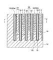
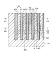
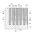
図1は、本実施形態に係る半導体装置1の図2におけるI−I線断面図であり、図2は、本実施形態に係る半導体装置1の図1におけるII−II線断面図である。換言すれば、図1は、半導体装置1におけるトレンチ直交方向の断面図であり、図2は、半導体装置1における平面方向の断面図である。
FIG. 1 is a sectional view taken along line II of FIG. 2 of the
これら図1及び図2から分かるように、本実施形態に係る半導体装置1は、複数のセルCを備えて構成されている。図1においては、5個のセルCを例示的に示しているが、半導体装置1が備えるセルCの数は任意である。
As can be seen from FIGS. 1 and 2, the
本実施形態に係る半導体装置1は、ドレイン電極10と、n+形のドレイン領域12と、n−形のドリフト領域14と、p形のベース領域16と、ゲート電極18と、ゲート絶縁膜20と、n+形のソース領域22と、絶縁領域24と、ソース電極26と、p+形のコンタクト領域28と、を備えて構成されている。すなわち、本実施形態においては、半導体装置1は、トレンチゲート形のMOSFETを備えて構成されている。
The
より具体的には、ドレイン電極10上には、ドレイン領域12が形成されている。ドレイン領域12上には、ドリフト領域14が形成されている。ドリフト領域14上には、ベース領域16が形成されている。これらドレイン電極10とドレイン領域12とドリフト領域14とベース領域16は、複数のセルCに対して共通に形成されている。
More specifically, the
ベース領域16上には、セルC毎に、ソース領域22が形成されている。また、セルC毎に、ソース領域22とベース領域16を貫通して、ドリフト領域14に達するゲート電極18が形成されている。このゲート電極18は、トレンチ長手方向に延伸している。各ゲート電極18の周囲には、ゲート絶縁膜20が形成されており、ゲート電極18と、その周囲との絶縁性を担保している。すなわち、ゲート電極18とドリフト領域14との間、ゲート電極18とベース領域16との間、及び、ゲート電極18とソース領域22との間に、ゲート絶縁膜20が形成されている。これらゲート電極18とゲート絶縁膜20とにより、ベース領域16が区分けされており、以下においては、1つの区分けされた領域をメサ部と呼ぶ。
A
ゲート電極18上、ソース領域22上及びゲート絶縁膜20上には、絶縁領域24が形成されている。絶縁領域24上には、ソース電極26が形成されている。本実施形態においては、絶縁領域24とソース電極26とを貫通して、ベース領域16に達するトレンチ30が各ゲート電極18の間に形成されており、このトレンチ30を埋めるように、ソース電極26が形成されている。このように、トレンチコンタクト構造となるようにソース電極26を形成することにより、ゲート構造を微細化してオン抵抗を低減しつつ、アバランシェ耐圧を高く維持できるようにしている。本実施形態においては、トレンチ30に埋め込まれたソース電極26の部分をコンタクト32と呼ぶこととする。
An
トレンチ30の底部に位置するベース領域16には、p+形のコンタクト領域28が形成されている。このコンタクト領域28の不純物濃度は、ベース領域16の不純物濃度より高くなるように形成されており、ソース電極26のコンタクト32とベース領域16との間の接続抵抗の低減を図っている。このため、コンタクト領域28は、省略することも理論上可能である。
A p + -
また、本実施形態に係る半導体装置1においては、終端領域の近傍のメサ部には、ソース領域22は形成されていないが、ソース電極26のコンタクト32は形成されている。以下においては、ソース領域22が形成されていない、終端領域の近傍にあるメサ部のコンタクト32を、適宜、コンタクト32aとし、一方、終端領域ではない、ソース領域22が形成されているメサ部のコンタクト32を、適宜、コンタクト32bとする。
Further, in the
さらに、終端領域の近接にあるメサ部のコンタクト32aの幅W1は、ソース領域22が形成されたメサ部のコンタクト32bの幅W2より、広い。すなわち、セルCを構成しない終端領域の近傍のメサ部に形成されたコンタクト32aの幅W1は、セルCを構成しているメサ部のコンタクト32bの幅W2よりも、広くなっている。
Further, the width W1 of the
終端領域の近傍のメサ部にセルCを形成しないのは、製造工程において、終端領域の近傍の領域は、フォトレジストの液だまり等が発生して、光リソグラフィーでセルCを形成するのに必要な精度が得にくいからである。また、本実施形態のように広い幅W1でコンタクト32aを形成することにより、逆回復時の動作において、終端領域に蓄積したホールを、この幅広のコンタクト32aから排出しやすくして、ホールの排出抵抗の低減を図っている。すなわち、ソース領域22が形成されているメサ部のコンタクト32bの幅W2を広げると、セルCにより構成されたMOSFETのチャネルとコンタクト領域28の距離が近くなり、MOSFETのしきい値が上昇してしまう。このため、コンタクト32bの幅W2を広げることは難しい。しかし、終端領域の近傍のメサ部には、ソース領域22が形成されないことから、コンタクト32aの幅W1を広げることができるのである。また、上述のように、終端領域付近は、配線等の段差により、フォトレジストの厚さが厚くなり、コンタクト32aを形成するための光リソグラフィーの際に、精度よく開口を形成しにくいという問題があるが、コンタクト32aの幅W1が広いことから、フォトレジストに開口を形成しやすくなる利点もある。
The reason why the cell C is not formed in the mesa portion near the terminal region is that in the manufacturing process, the region near the terminal region is necessary for forming the cell C by photolithography due to the generation of a photoresist liquid pool or the like. This is because it is difficult to obtain accurate accuracy. Further, by forming the
次に、本実施形態に係る半導体装置1の動作原理について説明する。例えば、ソース電極26よりも高い所定の正の電圧をドレイン電極10に印加する。この状態で、ゲート電極18にしきい値以上の電圧が印加されると、セルCに形成されたMOSFETがオン状態となる。このとき、ベース領域16におけるゲート絶縁膜20の近傍に、チャネルが形成される。その後、ゲート絶縁膜20がしきい値未満になると、セルCに形成されたMOSFETはオフ状態となる。
Next, the operating principle of the
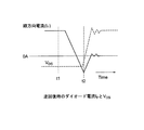
また、半導体装置1のボディーダイオードに、順方向の電流が流れていた状態で、この電流の流れが逆方向に切り替わるような逆回復時には、瞬間的にボディーダイオードに逆方向の電流が流れる。図3は、逆回復時における、ボディーダイオード電流IFと時間の関係と、ドレイン・ソース電圧VDSと時間の関係とを表すグラフを示す図である。この図3に示すように、逆回復時には、ボディーダイオードの逆方向に電流が流れるが、逆回復に必要な時間が経過すると、逆方向に流れる電流はゼロとなる。
Further, in a state where a forward current is flowing through the body diode of the
すなわち、時刻t1においては、図4に示すように、ボディーダイオードの順方向に電流が流れ、ドリフト領域14にホールが注入される。ドリフト領域14に注入されたホールはドレイン電極10に流れるが、ホールの一部は、半導体装置1の終端領域に蓄積される。しかし、図5に示すように、時刻t2の逆回復時には、ごく短い時間ではあるが、ボディーダイオードの逆方向に電流が流れる。この逆回復時には、ドリフト領域14に蓄積されたホールがコンタクト32から排出されるが、終端領域に蓄積されたホールは、ソース電極26のコンタクト32aまでの距離が遠く、排出されるための抵抗が高くなってしまう。そこで、本実施形態においては、終端領域の近傍にあるコンタクト32aの幅W1を広くして、ホールがソース電極26のコンタクト32aから排出されやすくし、排出抵抗を低減している。これにより、ゲート絶縁膜20が破壊されたり、電流集中による発熱を原因とする発破壊されたりするのを、抑制している。
That is, at time t1, as shown in FIG. 4, a current flows in the forward direction of the body diode, and a hole is injected into the
次に、図6乃至図16に基づいて、本実施形態に係る半導体装置1の製造工程の一例を説明する。これら図6乃至図16は、半導体装置1におけるトレンチ直交方向の断面図であり、上述した図1に対応する図である。
Next, an example of the manufacturing process of the
まず、図6に示すように、n+形の半導体基板12X上に、n−形の半導体層14Xを形成する。半導体基板12Xが、上述したドレイン領域12となり、半導体層14Xが、上述したドリフト領域14となる。
First, as shown in FIG. 6, on the n +
次に、図7に示すように、ドリフト領域14に、複数のトレンチ50を形成する。続いて、図8に示すように、トレンチ50を含むドリフト領域14の表面に、例えば熱酸化やCVD(Chemical Vapor Deposition)により、ゲート絶縁膜20を形成する。
Next, as shown in FIG. 7, a plurality of
次に、図9に示すように、ゲート絶縁膜20上に、例えばCVDによりポリシリコンを堆積し、エッチバックすることにより、トレンチ50に充填されたポリシリコンで、ゲート電極18を形成する。
Next, as shown in FIG. 9, polyvinyl is deposited on the
次に、図10に示すように、例えばボロン(B)をドリフト領域14にイオン注入することにより、ドリフト領域14に、ベース領域16を形成する。このボロンのイオン注入によるベース領域16の形成は、セルCを形成するメサ部と、セルCを形成しない終端領域の近傍のメサ部の双方に対して行う。続いて、例えばリン(P)又はヒ素(As)のイオン注入を、ベース領域16の上部に行い、n+形の半導体領域22Xを形成する。この半導体領域22Xの形成は、セルCが形成されるメサ部に対して行われる。すなわち、セルCを形成しない終端領域の近傍のメサ部には、半導体領域22Xは形成しない。
Next, as shown in FIG. 10, for example, by ion-implanting boron (B) into the
次に、図11に示すように、例えばCVDにより、この半導体装置の全体上に、絶縁膜24Xを形成する。続いて、図12に示すように、絶縁膜24X上に、フォトレジスト52を形成する。このフォトレジスト52は、例えば、フォトレジスト液をスピンコートで塗布するが、その際、終端領域の近傍では、どうしても液だまり等が発生しやすく、フォトレジスト52の膜厚むらが生じやすくなる。
Next, as shown in FIG. 11, an insulating
次に、図13に示すように、フォトレジスト52を光リソグラフィーでパターニングして、フォトレジスト52に開口52a、52bを形成する。この開口52a、52bは、ソース電極26のコンタクト32を形成すべき位置に形成される。また、開口52aは、フォトレジスト52の膜厚にばらつきがある終端領域の近傍に形成されることから、精度を担保するのが難しい。このため、コンタクト不良等が発生やすいが、本実施形態においては、終端領域の近傍のメサ部に形成されるコンタクト32aの幅W1は、セルCが存在するメサ部に形成されるコンタクト32bの幅W2よりも広い。このため、終端領域の近傍のメサ部の開口52aの幅の方を、セルを形成するメサ部の開口52bよりも、広くすることができる。本実施形態においては、開口52aも幅の広い幅W1で形成され、開口52bも幅の狭い幅W2で形成される。これにより、終端領域の近傍のメサ部に形成するコンタクト32aに、コンタクト不良が発生する確率を低減している。
Next, as shown in FIG. 13, the
次に、図14に示すように、例えばRIEにより、絶縁膜24Xをエッチングして、絶縁膜24Xをパターニングする。これにより、絶縁領域24が形成される。続いて、図15に示すように、例えばRIEにより、半導体領域22Xとベース領域16をエッチングして、絶縁領域24と半導体領域22Xとを貫通して、ベース領域16に達するトレンチ30を形成する。エッチングされた半導体領域22Xにより、ソース領域22が形成される。そして、フォトレジスト52を剥離する。
Next, as shown in FIG. 14, the insulating
次に、図16に示すように、トレンチ30を介してベース領域16に、例えばボロン(B)のイオン注入をすることにより、トレンチ30の底部で露出しているベース領域16にコンタクト領域28を形成する。
Next, as shown in FIG. 16, the
次に、図1及び図2に示すように、トレンチ30を埋めるように絶縁領域24上にソース電極26を形成し、ドレイン領域12下側にドレイン電極10を形成する。具体的には、例えば、表面メタルを形成して加工し、パッシベーション膜を形成した後に、ウェハーの薄膜化を行う。これにより、ソース電極26が形成される。さらに、裏面メタルを生成することにより、ドレイン電極10が形成され、図1及び図2に示した、半導体装置1が得られる。
Next, as shown in FIGS. 1 and 2, the
なお、本実施形態に係るドレイン領域12及び/又はドリフト領域14が、第1半導体領域に相当しており、本実施形態に係るソース領域22が形成されたメサ部が、第1領域に相当しており、本実施形態に係るソース領域22が形成されていないメサ部が、第2領域に相当しており、本実施形態に係るコンタクト32bが第1コンタクトに相当しており、本実施形態に係るコンタクト32aが第2コンタクトに相当している。また、コンタクト32bの幅W2が第1の幅に相当しており、コンタクト32aの幅W1が第2の幅に相当している。
The
以上のように、本実施形態に係る半導体装置1によれば、セルCの形成されない終端領域の近傍にあるメサ部におけるソース電極26のコンタクト32aの幅W1を、セルCの形成されるメサ部におけるソース電極26のコンタクト32bの幅W2よりも、広くなるようにしたので、MOSFETの逆回復時における電圧上昇を起因とするゲート絶縁膜20の破壊を生じにくくすることができる。また、MOSFETの逆回復時には、終端領域の近傍にあるコンタクト32aに電流が集中するが、コンタクト32aを幅広の幅W1にしたことにより、発熱を抑制し、半導体装置1の破損を防止することができる。
As described above, according to the
〔第2実施形態〕
第2実施形態は、上述した第1実施形態に係る半導体装置1において、トレンチ長手方向の終端部における、セルCのソース領域22が形成されていない領域にあるコンタクト32の幅も広げることにより、逆回復時における終端部からのホール排出抵抗の低減を図ったものである。以下、上述した第1実施形態と異なる部分を説明する。
[Second Embodiment]
In the second embodiment, in the
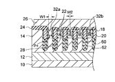
図17は、本実施形態に係る半導体装置1における平面方向の断面図であり、上述した第1実施形態における図2に対応する図である。この図17に示すように、本実施形態に係る半導体装置1においては、トレンチ長手方向の終端部、つまり、コンタクト32が延びる方向の終端部には、ソース領域22が形成されていない。これは、上述したように、光リソグラフィーの精度を担保するのが難しいからであるが、本実施形態に係る半導体装置1において、このトレンチ長手方向の終端部にあるコンタクト32の幅を、上述した幅W2よりも広い幅W3としている。以下では、幅W3のコンタクト32の部分を、コンタクト32cとする。このコンタクト32cは、ソース電極26と一体のメタルにより形成されているが、換言すれば、コンタクト32cは電気的にコンタクト32bと接続されており、また、ソース電極26に電気的に接続されている。
FIG. 17 is a sectional view in a plane direction of the
なお、コンタクト32cの幅W3は、コンタクト32aの幅W1と同じでもよいし、異なっていてもよい。また、コンタクト32cは、図示しないコンタクト32bの反対側の終端部にも形成されていてもよい。
The width W3 of the
このコンタクト32cが存在することにより、逆回復時には、ソース電極26のコンタクト32aだけでなく、コンタクト32cからもホールを排出できるので、ドリフト領域14に蓄積されたホールがより排出しやすくなり、ホールの排出抵抗を低減することができる。このため、MOSFETの逆回復時における電圧上昇を起因とするゲート絶縁膜20の破壊を生じにくくすることができる。
Due to the presence of the
なお、本実施形態に係るコンタクト32cが第3コンタクトに相当しており、本実施形態に係るコンタクト32cの幅W3が第3の幅に相当している。
The
〔第3実施形態〕
第3実施形態は、上述した第1実施形態に係る半導体装置1において、コンタクト32を、ソース電極26の一部であるメタルにより形成するのではなく、p+形の半導体領域により形成するようにしたものである。以下、上述した第1実施形態と異なる部分を説明する。
[Third Embodiment]
In the third embodiment, in the
図18は、本実施形態に係る半導体装置1におけるトレンチ直交方向の断面図であり、上述した第1実施形態における図1に対応する図である。この図18に示すように、本実施形態においては、ソース電極26とベース領域16との間を電気的に接続するコンタクト32が、p+形の半導体領域により形成されている。すなわち、上述した第1実施形態においては、コンタクト32は、ソース電極26を形成するメタルにより構成されていた。しかし、本実施形態においては、コンタクト32は、ベース領域16に多段イオン注入等により形成されたp+形の半導体領域により構成されている。
FIG. 18 is a cross-sectional view of the
本実施形態においても、ソース領域22が形成されない終端領域の近傍のメサ部に形成されたコンタクト32の幅W1は、ソース領域22が存在するメサ部に形成されたコンタクト32の幅W2よりも、幅広に構成されている。このため、上述した第1実施形態と同様に、ホールの排出抵抗を低減することができる。なお、本実施形態においては、コンタクト領域28はベース領域16に形成されていないが、p++形のコンタクト領域28を、コンタクト32の下端に位置するベース領域16に形成することも可能である。
Also in this embodiment, the width W1 of the
次に、本実施形態に係る半導体装置1の製造工程を説明する。本実施形態に係る半導体装置1の製造工程は、上述した第1実施形態に係る半導体装置1の図14に示す工程までは同じである。この図14の後、図19に示すように、例えばボロン(B)等の多段のイオン注入をベース領域16に行い、コンタクト32を形成する。すなわち、イオン注入の深さを適宜変えて、複数回、ベース領域16にイオン注入を行う。
Next, the manufacturing process of the
その際、フォトレジスト52に形成された開口52aの幅W1は、開口52bの幅W2よりも広く形成されている。このため、終端領域の近傍のメサ部には、広い幅W1でコンタクト32aが形成され、ソース領域22が形成されてセルCを構成するメサ部には、狭い幅W2でコンタクト32bが形成される。そして、フォトレジスト52を剥離する。この後、上述した第1実施形態と同様に、半導体装置1の表面にソース電極26を形成し、半導体装置1の裏面にドレイン電極10を形成することにより、図18に示す半導体装置1が得られる。
At that time, the width W1 of the
以上のように、本実施形態に係る半導体装置1によっても、セルCの形成されない終端領域の近傍にあるメサ部におけるソース電極26のコンタクト32aの幅W1を、セルCの形成されるメサ部におけるソース電極26のコンタクト32bの幅W2よりも、広くなるようにしたので、MOSFETの逆回復時における電圧上昇を起因とするゲート絶縁膜20の破壊を生じにくくすることができる。また、MOSFETの逆回復時には、終端領域の近傍にあるコンタクト32aに電流が集中するが、コンタクト32aを幅広にしたことにより、発熱を抑制し、半導体装置1の破損を防止することができる。
As described above, also in the
なお、本実施形態に係るコンタクト32aとコンタクト32bが、第2半導体領域に相当する。
The
〔第4実施形態〕
第4実施形態は、上述した第1実施形態を変形して、ゲート電極18の下方に埋め込みの電極を形成したトレンチフィールドプレート構造にしたものである。以下、上述した第1実施形態と異なる部分を説明する。
[Fourth Embodiment]
The fourth embodiment is a modification of the above-mentioned first embodiment to have a trench field plate structure in which an embedded electrode is formed below the
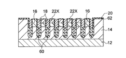
図20は、本実施形態に係る半導体装置1におけるトレンチ直交方向の断面図であり、上述した第1実施形態の図1に対応する図である。図21は、図20の半導体装置1におけるXXI−XXI線断面図であり、上述した第1実施形態の図2に対応する図である。図22は、図21の半導体装置1におけるXXII−XXII線断面図であり、図23は、図21の半導体装置1におけるXXIII−XXIII線断面図である。
FIG. 20 is a cross-sectional view of the
これら図20乃至図23に示すように、本実施形態に係る半導体装置1は、ゲート電極18のそれぞれの下方における、ドリフト領域14にフィールドプレート電極60が埋め込まれている。すなわち、ドリフト領域14の中にフィールドプレート絶縁膜62を介して、フィールドプレート電極60が埋め込まれている。フィールドプレート絶縁膜62は、フィールドプレート電極60の周囲を囲うように形成されているが、フィールドプレート電極60は、電気的にはゲート電極18又はソース電極26に接続されている。また、フィールドプレート絶縁膜62の厚さは、ゲート絶縁膜20の厚さより、厚く形成されている。
As shown in FIGS. 20 to 23, in the
このフィールドプレート電極60が存在するMOSFETの構造を、トレンチフィールドプレート構造というが、別名、スプリットゲート構造と言ったり、シールドゲート構造と言ったりする。このフィールドプレート電極60が存在することにより、ドリフト領域14にあるイオン化ドナーの正電荷をキャンセルすることができ、ドリフト領域14内の空間電荷が実質的なゼロに見えて、電界がフラットに近づくため、この半導体装置1の耐圧が向上する。また、ドリフト領域14の不純物濃度は、ゲート電極18同士の幅、つまりメサ部の幅に反比例して高くすることができるため、セルCのピッチシュリンクにより不純物濃度を高めることで、ドリフト領域14の抵抗を低減することができる。
The structure of the MOSFET in which the
なお、図21及び図23に示すように、ソース電極26のコンタクト32のトレンチ長手方向の終端部には、ソース領域22は形成されていない。これは、フィールドプレート絶縁膜62とゲート絶縁膜20とから形成された絶縁膜の膜厚が厚いことから、フォトレジストを形成した際に、液だまりが生じて、精度よく開口を形成することができず、高い精度でMOSFETを形成することができないためである。
As shown in FIGS. 21 and 23, the
次に、図24乃至図37に基づいて、本実施形態に係る半導体装置1の製造工程を説明する。これら図24乃至図37は、半導体装置1におけるトレンチ直交方向の断面図であり、上述した図20に対応する図である。
Next, the manufacturing process of the
まず、図24に示すように、n+形の半導体基板12X上に、n−形の半導体層14Xを形成する。半導体基板12Xが、上述したドレイン領域12となり、半導体層14Xが、上述したドリフト領域14となる。
First, as shown in FIG. 24, on the n +
次に、図25に示すように、ドリフト領域14に、複数のトレンチ70を形成する。このトレンチ70は、後の工程でフィールドプレート電極60を形成することから、第1実施形態におけるトレンチ50よりも深く形成される。続いて、図26に示すように、トレンチ70を含むドリフト領域14の表面に、例えば熱酸化やCVDにより、フィールドプレート絶縁膜62を形成する。上述したように、このフィールドプレート絶縁膜62は、ゲート電極18よりも厚い膜厚を有している。
Next, as shown in FIG. 25, a plurality of
次に、図27に示すように、フィールドプレート絶縁膜62上に、例えばCVDによりポリシリコンを堆積し、エッチバックすることにより、トレンチ70に充填されたポリシリコンで、フィールドプレート電極60を形成する。
Next, as shown in FIG. 27, the polysilicon is deposited on the field
次に、図28に示すように、光リソグラフィーによりパターニングされたフォトレジスト74を形成する。このフォトレジスト74は、ソース領域22を形成するメサ部に開口74aを有している。なお、ソース領域22を形成しない最も終端領域の近傍にあるメサ部の終端領域側のフィールドプレート絶縁膜62は、フォトレジスト74で覆われている。その後、例えばウエットエッチングにより、開口74aから露出しているフィールドプレート絶縁膜62を除去する。このため、終端領域にあるトレンチ70の終端領域側の側壁に形成されたフィールドプレート絶縁膜62の絶縁膜も、フォトレジスト74に覆われていることから、エッチングされずに残る。
Next, as shown in FIG. 28, a
次に、図29に示すように、フォトレジスト74を剥離し、例えば熱酸化又はCVDにより、この半導体装置の全体上にゲート絶縁膜20を形成する。すなわち、トレンチ70の内側と、フィールドプレート電極60の上に、ゲート絶縁膜20を形成する。このときに、終端領域には、フィールドプレート絶縁膜62が残存しているので、このフィールドプレート絶縁膜62の上に、ゲート絶縁膜20が形成される。このため、終端領域の絶縁膜の厚さは、セルCが形成される領域の絶縁膜の厚さより厚くなる。また、終端領域にあるトレンチ70の終端側の側壁の絶縁膜も、残存するフィールドプレート絶縁膜62とゲート絶縁膜20とを合わせた厚さとなる。なお、膜厚調整等の必要に応じて、フィールドプレート電極60の上に選択的に絶縁膜を形成する工程を行ってもよい。
Next, as shown in FIG. 29, the
次に、図30に示すように、例えばCVDによりポリシリコンを形成し、エッチバックすることにより、トレンチ70の残っている空間にポリシリコンを充填して、ゲート絶縁膜20を形成する。
Next, as shown in FIG. 30, for example, polysilicon is formed by CVD and etched back to fill the remaining space of the
次に、図31に示すように、例えばボロン(B)をドリフト領域14にイオン注入することにより、ドリフト領域14に、ベース領域16を形成する。このボロンのイオン注入によるベース領域16の形成は、セルCを形成するメサ部と、セルCを形成しない終端領域の近傍のメサ部の双方に対して行う。続いて、例えばリン(P)又はヒ素(As)のイオン注入を、ベース領域16の上部に行い、n+形の半導体領域22Xを形成する。この半導体領域22Xの形成は、セルCが形成されるメサ部に対して行われる。すなわち、セルCを形成しない終端領域の近傍のメサ部には、半導体領域22Xは形成しない。
Next, as shown in FIG. 31, for example, by ion-implanting boron (B) into the
次に、図32に示すように、例えばCVDにより、この半導体装置の全体上に、絶縁膜24Xを形成する。この際、終端領域の近傍には、ゲート絶縁膜20とフィールドプレート絶縁膜62とから形成された絶縁膜とゲート絶縁膜20との段差が存在することから、絶縁膜24Xにも段差が形成される。
Next, as shown in FIG. 32, the insulating
次に、図33に示すように、絶縁膜24X上に、フォトレジスト52を形成する。このフォトレジスト52は、例えば、フォトレジスト液をスピンコートで塗布するが、その際、終端領域の近傍では、どうしても液だまり等が発生しやすく、フォトレジスト52の膜厚むらが生じやすくなる。
Next, as shown in FIG. 33, the
次に、図34に示すように、フォトレジスト52を光リソグラフィーでパターニングして、フォトレジスト52に開口52a、52bを形成する。この開口52a、52bは、ソース電極26のコンタクト32を形成すべき位置に形成される。また、開口52aは、フォトレジスト52の膜厚にばらつきがある終端領域の近傍に形成されることから、精度を担保するのが難しい。このため、コンタクト不良等が発生やすいが、本実施形態においては、終端領域の近傍のメサ部に形成されるコンタクト32aの幅W1は、セルCが存在するメサ部に形成されるコンタクト32bの幅W2よりも広い。このため、終端領域の近傍のメサ部の開口52aの幅の方を、セルを形成するメサ部の開口52bよりも、広くすることができる。本実施形態においては、開口52aも幅の広い幅W1で形成され、開口52bも幅の狭い幅W2で形成される。これにより、終端領域の近傍のメサ部に形成するコンタクト32aに、コンタクト不良が発生する確率を低減している。
Next, as shown in FIG. 34, the
次に、図35に示すように、例えばRIEにより、絶縁膜24Xをエッチングして、絶縁膜24Xをパターニングする。これにより、絶縁領域24が形成される。続いて、図36に示すように、例えばRIEにより、半導体領域22Xとベース領域16をエッチングして、絶縁領域24と半導体領域22Xとを貫通して、ベース領域16に達するトレンチ30を形成する。エッチングされた半導体領域22Xにより、ソース領域22が形成される。そして、フォトレジスト52を剥離する。
Next, as shown in FIG. 35, the insulating
次に、図37に示すように、トレンチ30を介してベース領域16に、例えばボロン(B)のイオン注入をすることにより、トレンチ30の底部で露出しているベース領域16にコンタクト領域28を形成する。この後、上述した第1実施形態と同様に、半導体装置1の表面にソース電極26を形成し、半導体装置1の裏面にドレイン電極10を形成することにより、図20に示す半導体装置1が得られる。
Next, as shown in FIG. 37, the
以上のように、本実施形態に係る半導体装置1によっても、ソース領域22の形成されない終端領域の近傍にあるメサ部におけるソース電極26のコンタクト32aの幅W1を、ソース領域22の形成されるメサ部におけるソース電極26のコンタクト32bの幅W2よりも、広くなるようにしたので、MOSFETの逆回復時における電圧上昇を起因とするゲート絶縁膜20の破壊を生じにくくすることができる。また、MOSFETの逆回復時には、終端領域の近傍にあるコンタクト32aに電流が集中するが、コンタクト32aを幅広にしたことにより、発熱を抑制し、半導体装置1の破損を防止することができる。
As described above, even in the
〔第5実施形態〕
第5実施形態は、上述した第2実施形態と第4実施形態とを組み合わせたものであり、第2実施形態に係るトレンチ長手方向の終端部に幅広のコンタクト32cを形成した半導体装置1を、トレンチフィールドプレート構造にしたものである。
[Fifth Embodiment]
The fifth embodiment is a combination of the second embodiment and the fourth embodiment described above, and is a
図38は、本実施形態に係る半導体装置1の平面方向の断面図であり、上述した第4実施形態の図21に相当する図である。図39は、本実施形態に係る半導体装置1の図38におけるXXXIX−XXXIX線断面図であり、上述した第4実施形態の図22に相当する図である。図40は、本実施形態に係る半導体装置1の図38におけるXL−XL線断面図であり、上述した第4実施形態の図23に相当する図である。
FIG. 38 is a sectional view taken along the plane of the
これら図38乃至図40に示すように、本実施形態に係る半導体装置1においては、上述した第2実施形態に係る半導体装置1に、フィールドプレート電極60を追加的に設けて構成されている。すなわち、ドリフト領域14の中にフィールドプレート絶縁膜62を介して、フィールドプレート電極60が埋め込まれている。フィールドプレート絶縁膜62は、フィールドプレート電極60の周囲を囲うように形成されているが、フィールドプレート電極60は、電気的にはゲート電極18又はソース電極26に接続されている。
As shown in FIGS. 38 to 40, in the
また、本実施形態に係る半導体装置1においても、トレンチ長手方向の終端部には、ソース領域22が形成されていない。これは、上述したように、光リソグラフィーの精度を担保するのが難しいからであるが、このトレンチ長手方向の終端部にあるコンタクト32cの幅を、幅W2によりも広い幅W3としている。なお、コンタクト32cの幅W3は、コンタクト32aの幅W1と同じでもよいし、異なっていてもよい。
Further, also in the
このように、フィールドプレート電極60をドリフト領域14に設けることにより、半導体装置1の耐圧を向上させつつ、ドリフト領域14の抵抗を低減することができる。また、幅広のコンタクト32aに加えて、幅広のコンタクト32cを設けることにより、このMOSFETの逆回復時に、ソース電極26のコンタクト32cから、さらにホールを排出しやすくし、ホールの排出抵抗を低減することができる。
By providing the
〔第6実施形態〕
第6実施形態は、上述した第3実施形態と第4実施形態とを組み合わせたものであり、第3実施形態に係るトレンチ長手方向の終端部に幅広のコンタクト32cを形成した半導体装置1を、トレンチフィールドプレート構造にしたものである。別な見方をすれば、上述した第5実施形態における半導体装置1において、コンタクト32をメタルではなく、p+形の半導体領域により形成したものである。
[Sixth Embodiment]
The sixth embodiment is a combination of the third embodiment and the fourth embodiment described above, and the
図41は、本実施形態に係る半導体装置1の平面方向の断面図であり、上述した第4実施形態の図21に相当する図である。図42は、本実施形態に係る半導体装置1の図41におけるXLII−XLII線断面図であり、上述した第4実施形態の図22に相当する図である。図43は、本実施形態に係る半導体装置1の図41におけるXLIII−XLIII線断面図であり、上述した第4実施形態の図23に相当する図である。
FIG. 41 is a sectional view taken along the plane of the
これら図41乃至図43に示すように、本実施形態に係る半導体装置1においては、上述した第3実施形態に係る半導体装置1に、フィールドプレート電極60を追加的に設けて構成されている。すなわち、ドリフト領域14の中にフィールドプレート絶縁膜62を介して、フィールドプレート電極60が埋め込まれている。フィールドプレート絶縁膜62は、フィールドプレート電極60の周囲を囲うように形成されているが、フィールドプレート電極60は、電気的にはゲート電極18又はソース電極26に接続されている。
As shown in FIGS. 41 to 43, in the
また、本実施形態に係る半導体装置1においては、ソース電極26とベース領域16との間を電気的に接続するコンタクト32が、p+形の半導体領域により形成されている。すなわち、上述した第5実施形態においては、コンタクト32は、ソース電極26を形成するメタルにより構成されていた。しかし、本実施形態においては、コンタクト32は、ベース領域16に多段イオン注入等により形成されたp+形の半導体領域により構成されている。
Further, in the
同様に、コンタクト32のトレンチ長手方向の終端部には、コンタクト32cが形成されているが、このコンタクト32cも、p+形の半導体領域により形成されている。このコンタクト32cの幅は、上述同様に、幅W2によりも広い幅W3としている。なお、コンタクト32cの幅W3は、コンタクト32aの幅W1と同じでもよいし、異なっていてもよい。
Similarly, a
このように、フィールドプレート電極60をドリフト領域14に設けることにより、半導体装置1の耐圧を向上させつつ、ドリフト領域14の抵抗を低減することができる。また、幅広のコンタクト32aに加えて、幅広のコンタクト32cを設けることにより、このMOSFETの逆回復時に、ソース電極26のコンタクト32cから、さらにホールを排出しやすくし、ホールの排出抵抗を低減することができる。
By providing the
なお、本実施形態に係るコンタクト32aとコンタクト32bとコンタクト32cとが、第3半導体領域に相当している。
The
〔第7実施形態〕
第7実施形態は、上述した第4実施形態の半導体装置1において、セルCの形成されない終端領域の近傍にあるメサ部における幅W1のコンタクト32aを、セルCの形成されるメサ部における幅W2のコンタクト32bよりも、深い位置まで形成し、より一層のホールの排出抵抗の低減を図ったものである。以下、上述した第4実施形態と異なる部分を説明する。
[7th Embodiment]
In the seventh embodiment, in the
図44は、本実施形態に係る半導体装置1の平面方向の断面図であり、上述した第4実施形態の図21に相当する図である。図45は、本実施形態に係る半導体装置1の図44におけるXLV−XLV線断面図であり、上述した第4実施形態の図22に相当する図である。図46は、本実施形態に係る半導体装置1の図44におけるXLVI−XLVI線断面図であり、上述した第4実施形態の図23に相当する図である。
FIG. 44 is a cross-sectional view of the
これら図44乃至図46に示すように、ソース領域22の形成されない終端領域の近傍にあるメサ部におけるソース電極26の幅W1のコンタクト32aを、ソース領域22の形成されるメサ部におけるソース電極26の幅W2のコンタクト32bよりも、深い位置まで形成されている。すなわち、コンタクト32aの深さDP1の方が、コンタクト32bの深さDP2よりも深い。つまり、本実施形態においては、このコンタクト32bの深さDP2は、上述した第4実施形態におけるコンタクト32bの深さと同じであるが、コンタクト32aの深さDP1は、上述した第4実施形態におけるコンタクト32aの深さよりも深い。
As shown in FIGS. 44 to 46, the
このように、ソース領域22の形成されない終端領域の近傍のメサ部にあるコンタクト32aの深さDP1を、ソース領域22の形成されるメサ部にあるコンタクト32bの深さDP2よりも、深くしたので、ホールの排出抵抗をさらに低減することができる。すなわち、コンタクト32aを介して、終端領域に蓄積したホールを、この幅広で深く形成されたコンタクト32aから排出しやすくして、ホールの排出抵抗の低減を図ることができる。
In this way, the depth DP1 of the
なお、この終端領域の近傍にある深さDP1のコンタクト32aを形成するためには、第4実施形態の図33乃至図36の製造工程において、コンタクト32aを形成するためのトレンチ30とコンタクト32bを形成するためのトレンチ30とを、それぞれ、深さDP1と深さDP2とで作り分ければよい。或いは、コンタクト32aのトレンチ30を形成するためのフォトレジスト52の開口52aの方が、コンタクト32bのトレンチ30を形成するためのフォトレジスト52の開口52bよりも、広いことから、これら開口52a、52bを通じてベース領域16を同時にエッチングしても、コンタクト32aのトレンチ30の方が、コンタクト32bのトレンチ30よりも深く形成される特性を利用してもよい。
In order to form the
〔第8実施形態〕
第8実施形態は、上述した第2実施形態と第7実施形態とを組み合わせたものであり、第7実施形態に係る半導体装置1のコンタクト32におけるトレンチ長手方向の終端部に、幅広のコンタクト32cを形成したものである。以下、上述した第7実施形態と異なる部分を説明する。
[Eighth Embodiment]
The eighth embodiment is a combination of the second embodiment and the seventh embodiment described above, and has a
図47は、本実施形態に係る半導体装置1の平面方向の断面図であり、上述した第7実施形態の図44に相当する図である。図48は、本実施形態に係る半導体装置1の図47におけるXLVIII−XLVIII線断面図であり、上述した第7実施形態の図45に相当する図である。図49は、本実施形態に係る半導体装置1の図47におけるXLIX−XLIX線断面図であり、上述した第7実施形態の図46に相当する図である。
FIG. 47 is a sectional view taken along the plane of the
これら図47乃至図49に示すように、本実施形態に係る半導体装置1においては、トレンチ長手方向の終端部にあるコンタクト32cの幅を、第2実施形態と同様に、幅W2によりも広い幅W3としている。なお、コンタクト32cの幅W3は、コンタクト32aの幅W1と同じでもよいし、異なっていてもよい。また、本実施形態においては、コンタクト32cが形成される深さDP1は、コンタクト32aが形成される深さDP1と同じであるが、コンタクト32cが形成される深さとコンタクト32aが形成される深さは異なっていてもよい。換言すれば、コンタクト32cが形成される深さとコンタクト32aが形成される深さが、それぞれ、コンタクト32bが形成される深さよりも深ければ足りる。
As shown in FIGS. 47 to 49, in the
このため、逆回復時には、ソース電極26のコンタクト32aだけでなく、コンタクト32cからホールを排出できるので、ホールがより排出しやすくなり、ホールの排出抵抗を低減することができる。このため、MOSFETの逆回復時における電圧上昇を起因とするゲート絶縁膜20の破壊を生じにくくすることができる。また、MOSFETの逆回復時には、終端領域の近傍にあるコンタクト32aに電流が集中するのを抑制して、半導体装置1の破損を防止することができる。
Therefore, at the time of reverse recovery, the hole can be discharged not only from the
以上、いくつかの実施形態を説明したが、これらの実施形態は、例としてのみ提示したものであり、発明の範囲を限定することを意図したものではない。本明細書で説明した新規な装置および方法は、その他の様々な形態で実施することができる。また、本明細書で説明した装置および方法の形態に対し、発明の要旨を逸脱しない範囲内で、種々の省略、置換、変更を行うことができる。添付の特許請求の範囲およびこれに均等な範囲は、発明の範囲や要旨に含まれるこのような形態や変形例を含むように意図されている。 Although some embodiments have been described above, these embodiments are presented only as examples and are not intended to limit the scope of the invention. The novel devices and methods described herein can be implemented in a variety of other forms. In addition, various omissions, substitutions, and changes can be made to the forms of the apparatus and method described in the present specification without departing from the gist of the invention. The appended claims and their equivalent scope are intended to include such forms and variations contained in the scope and gist of the invention.
例えば、上述した各実施形態においては、ソース領域22の形成されていない終端領域のメサ部が、トレンチ直交方向の両側に1つずつ設けられている例を説明したが、ソース領域22の形成されていないメサ部の数は任意である。例えば、トレンチ直交方向の両側に2つずつ、ソース領域22が形成されないメサ部が設けられている場合には、それぞれのメサ部に広い幅W1を有するコンタクト32aを形成すればよい。
For example, in each of the above-described embodiments, the example in which one mesa portion of the terminal region in which the
1:半導体装置、10:ドレイン電極、12:ドレイン領域、14:ドリフト領域、16:ベース領域、18:ゲート電極、20:ゲート絶縁膜、22:ソース領域、24:絶縁領域、26:ソース電極、28:コンタクト領域、30:トレンチ、32:コンタクト、C:セル 1: Semiconductor device, 10: Drain electrode, 12: Drain region, 14: Drift region, 16: Base region, 18: Gate electrode, 20: Gate insulating film, 22: Source region, 24: Insulation region, 26: Source electrode , 28: Contact area, 30: Trench, 32: Contact, C: Cell
Claims (12)
前記第1半導体領域の上に形成された第2導電形のベース領域と、
前記ベース領域を貫通して前記第1半導体領域に達する、複数のゲート電極と、
前記複数のゲート電極のそれぞれの周囲に形成された、複数のゲート絶縁膜と、
前記複数のゲート絶縁膜の間である複数の領域のうち、2つの前記ゲート絶縁膜の間に位置する第1領域であって、第1導電形のソース領域が形成された第1領域と、
前記複数の領域のうち、2つの前記ゲート絶縁膜の間に位置する第2領域であって、前記第1領域の終端領域に位置し、前記ソース領域が形成されていない第2領域と、
前記第1領域に形成されて、前記ベース領域とソース電極とを電気的に接続する、第1の幅の第1コンタクトと、
前記第2領域に形成されて、前記ベース領域と前記ソース電極とを電気的に接続する、前記第1の幅よりも広い第2の幅の第2コンタクトと、
を備え、
前記ベース領域、前記ゲート電極、前記ゲート絶縁膜、前記第1領域、前記第2領域、前記第1コンタクト、及び、前記第2コンタクトは、第1方向に沿って連続して形成されており、
前記第2領域は、前記第1方向と交差する方向である第2方向の両側に設けられ、これら両側に設けられた前記第2領域のそれぞれに1つの前記第2コンタクトが形成されているとともに、これら前記第2領域の間には複数の前記第1領域が形成されており、
複数の前記第1領域のそれぞれに形成された前記第1コンタクトにおける前記第1方向の両端の終端部に、前記第1の幅よりも広い第3の幅で第3コンタクトがそれぞれ形成されている、半導体装置。 The first semiconductor region of the first conductive type and
The second conductive type base region formed on the first semiconductor region and
A plurality of gate electrodes that penetrate the base region and reach the first semiconductor region,
A plurality of gate insulating films formed around each of the plurality of gate electrodes, and a plurality of gate insulating films.
Of the plurality of regions between the plurality of gate insulating films, the first region located between the two gate insulating films, the first region in which the source region of the first conductive type is formed, and the first region.
Of the plurality of regions, a second region located between the two gate insulating films, which is located at the terminal region of the first region and in which the source region is not formed, and a second region.
A first contact having a first width, which is formed in the first region and electrically connects the base region and the source electrode.
A second contact having a second width wider than the first width, which is formed in the second region and electrically connects the base region and the source electrode.
Equipped with
The base region, the gate electrode, the gate insulating film, the first region, the second region, the first contact, and the second contact are continuously formed along the first direction.
The second region is provided on both sides of the second direction, which is a direction intersecting the first direction, and one second contact is formed in each of the second regions provided on both sides. A plurality of the first regions are formed between the second regions.
A third contact having a third width wider than the first width is formed at the end portions of both ends of the first contact in the first contact formed in each of the plurality of first regions. , Semiconductor equipment.
前記第1領域に形成される前記第1コンタクトの深さよりも、前記第1コンタクトが延びる方向の終端部に形成された前記第3コンタクトの深さの方が深い、
請求項3に記載の半導体装置。 The depth of the second contact formed in the second region is deeper than the depth of the first contact formed in the first region, and
The depth of the third contact formed at the end in the direction in which the first contact extends is deeper than the depth of the first contact formed in the first region.
The semiconductor device according to claim 3.
前記第1領域に形成される前記第1コンタクトの深さよりも、前記第2領域に形成される前記第2コンタクトの深さの方が深い、請求項1に記載の半導体装置。 The first contact and the second contact are made of metal formed in a trench reaching the base region.
The semiconductor device according to claim 1, wherein the depth of the second contact formed in the second region is deeper than the depth of the first contact formed in the first region.
前記第3コンタクトの前記第3の幅は、前記第2コンタクトの前記第2の幅と同じであり、
前記第1領域に形成される前記第1コンタクトの深さよりも、前記第2領域に形成される前記第2コンタクトの深さの方が深く、且つ、
前記第1領域に形成される前記第1コンタクトの深さよりも、前記第1コンタクトが延びる方向の終端部に形成された前記第3コンタクトの深さの方が深い、
請求項1に記載の半導体装置。 The first contact, the second contact, and the third contact are made of metal formed in a trench reaching the base region.
The third width of the third contact is the same as the second width of the second contact.
The depth of the second contact formed in the second region is deeper than the depth of the first contact formed in the first region, and
The depth of the third contact formed at the end in the direction in which the first contact extends is deeper than the depth of the first contact formed in the first region.
The semiconductor device according to claim 1.
Priority Applications (5)
| Application Number | Priority Date | Filing Date | Title |
|---|---|---|---|
| JP2018050096A JP6970632B2 (en) | 2018-03-16 | 2018-03-16 | Semiconductor device |
| CN202210727614.4A CN115101597A (en) | 2018-03-16 | 2018-08-20 | Semiconductor device with a plurality of semiconductor chips |
| CN201810946471.XA CN110277448B (en) | 2018-03-16 | 2018-08-20 | Semiconductor device with a plurality of semiconductor chips |
| US16/126,668 US10593793B2 (en) | 2018-03-16 | 2018-09-10 | Semiconductor device |
| JP2021176918A JP7284797B2 (en) | 2018-03-16 | 2021-10-28 | semiconductor equipment |
Applications Claiming Priority (1)
| Application Number | Priority Date | Filing Date | Title |
|---|---|---|---|
| JP2018050096A JP6970632B2 (en) | 2018-03-16 | 2018-03-16 | Semiconductor device |
Related Child Applications (1)
| Application Number | Title | Priority Date | Filing Date |
|---|---|---|---|
| JP2021176918A Division JP7284797B2 (en) | 2018-03-16 | 2021-10-28 | semiconductor equipment |
Publications (3)
| Publication Number | Publication Date |
|---|---|
| JP2019161190A JP2019161190A (en) | 2019-09-19 |
| JP2019161190A5 JP2019161190A5 (en) | 2020-03-26 |
| JP6970632B2 true JP6970632B2 (en) | 2021-11-24 |
Family
ID=67906119
Family Applications (1)
| Application Number | Title | Priority Date | Filing Date |
|---|---|---|---|
| JP2018050096A Active JP6970632B2 (en) | 2018-03-16 | 2018-03-16 | Semiconductor device |
Country Status (3)
| Country | Link |
|---|---|
| US (1) | US10593793B2 (en) |
| JP (1) | JP6970632B2 (en) |
| CN (2) | CN110277448B (en) |
Families Citing this family (3)
| Publication number | Priority date | Publication date | Assignee | Title |
|---|---|---|---|---|
| JP7249269B2 (en) * | 2019-12-27 | 2023-03-30 | 株式会社東芝 | Semiconductor device and its manufacturing method |
| FR3128312A1 (en) * | 2021-10-20 | 2023-04-21 | Stmicroelectronics S.R.L. | Electronic device comprising transistors |
| CN116364755A (en) * | 2023-03-14 | 2023-06-30 | 瑶芯微电子科技(上海)有限公司 | Shielded gate trench type MOSFET device and manufacturing method thereof |
Family Cites Families (22)
| Publication number | Priority date | Publication date | Assignee | Title |
|---|---|---|---|---|
| JP3405649B2 (en) * | 1996-12-05 | 2003-05-12 | 株式会社東芝 | Semiconductor device |
| JP2001094104A (en) * | 1999-09-24 | 2001-04-06 | Toshiba Corp | Power semiconductor element |
| JP4696335B2 (en) * | 2000-05-30 | 2011-06-08 | 株式会社デンソー | Semiconductor device and manufacturing method thereof |
| US7566622B2 (en) * | 2005-07-06 | 2009-07-28 | International Rectifier Corporation | Early contact, high cell density process |
| JP5055786B2 (en) * | 2006-02-20 | 2012-10-24 | 富士電機株式会社 | MOS type semiconductor device and manufacturing method thereof |
| JP5222466B2 (en) * | 2006-08-09 | 2013-06-26 | ルネサスエレクトロニクス株式会社 | Semiconductor device and manufacturing method thereof |
| JP2011100877A (en) * | 2009-11-06 | 2011-05-19 | Toshiba Corp | Semiconductor device and method of manufacturing the same |
| JP5672766B2 (en) | 2010-05-17 | 2015-02-18 | 株式会社デンソー | Semiconductor device |
| JP5560991B2 (en) | 2010-07-23 | 2014-07-30 | 株式会社デンソー | Semiconductor device |
| JP2012204395A (en) * | 2011-03-23 | 2012-10-22 | Toshiba Corp | Semiconductor device and manufacturing method of the same |
| JP6271155B2 (en) * | 2013-05-21 | 2018-01-31 | 株式会社東芝 | Semiconductor device |
| CN104995738B (en) | 2013-08-15 | 2018-01-23 | 富士电机株式会社 | Semiconductor device |
| CN105210187B (en) * | 2013-10-04 | 2017-10-10 | 富士电机株式会社 | Semiconductor device |
| CN105531825B (en) * | 2013-12-16 | 2019-01-01 | 富士电机株式会社 | The manufacturing method of semiconductor device and semiconductor device |
| JP6448434B2 (en) * | 2015-03-25 | 2019-01-09 | ルネサスエレクトロニクス株式会社 | Semiconductor device and manufacturing method thereof |
| JP6509673B2 (en) * | 2015-08-10 | 2019-05-08 | 株式会社東芝 | Semiconductor device |
| DE102015118524B4 (en) * | 2015-10-29 | 2022-01-27 | Infineon Technologies Ag | Insulated gate semiconductor device with soft switching behavior and method of manufacturing the same |
| JP6378220B2 (en) * | 2016-02-01 | 2018-08-22 | 株式会社東芝 | Semiconductor device |
| JP6507112B2 (en) * | 2016-03-16 | 2019-04-24 | 株式会社東芝 | Semiconductor device |
| JP6739372B2 (en) * | 2017-02-21 | 2020-08-12 | 株式会社東芝 | Semiconductor device |
| JP6872951B2 (en) * | 2017-03-30 | 2021-05-19 | エイブリック株式会社 | Semiconductor devices and their manufacturing methods |
| US20180337172A1 (en) * | 2017-05-19 | 2018-11-22 | Sanken Electric Co., Ltd. | Semiconductor Device |
-
2018
- 2018-03-16 JP JP2018050096A patent/JP6970632B2/en active Active
- 2018-08-20 CN CN201810946471.XA patent/CN110277448B/en active Active
- 2018-08-20 CN CN202210727614.4A patent/CN115101597A/en active Pending
- 2018-09-10 US US16/126,668 patent/US10593793B2/en active Active
Also Published As
| Publication number | Publication date |
|---|---|
| CN110277448A (en) | 2019-09-24 |
| US10593793B2 (en) | 2020-03-17 |
| JP2019161190A (en) | 2019-09-19 |
| CN110277448B (en) | 2022-07-26 |
| US20190288103A1 (en) | 2019-09-19 |
| CN115101597A (en) | 2022-09-23 |
Similar Documents
| Publication | Publication Date | Title |
|---|---|---|
| US10186609B2 (en) | Semiconductor device, RC-IGBT, and method of manufacturing semiconductor device | |
| US9385202B2 (en) | Semiconductor device having a patterned gate dielectric | |
| US7999314B2 (en) | Semiconductor device and manufacturing method thereof | |
| US7893489B2 (en) | Semiconductor device having vertical MOSFET | |
| US6972458B2 (en) | Horizontal MOS transistor | |
| US7663182B2 (en) | Vertical trench gate transistor semiconductor device and method for fabricating the same | |
| US6919249B2 (en) | Semiconductor device and its manufacturing method comprising a trench gate | |
| JP6666671B2 (en) | Semiconductor device | |
| US9722071B1 (en) | Trench power transistor | |
| US10903202B2 (en) | Semiconductor device | |
| JP6970632B2 (en) | Semiconductor device | |
| CN111370487B (en) | Trench gate MOSFET device and manufacturing method thereof | |
| US20200168714A1 (en) | Semiconductor device and method for manufacturing the same | |
| US20200105946A1 (en) | Diode structure | |
| JP2010087096A (en) | Semiconductor device and method for manufacturing the same | |
| CN113614883B (en) | Semiconductor device with a semiconductor device having a plurality of semiconductor chips | |
| US20130252423A1 (en) | Method for manufacturing a semiconductor device and semiconductor device | |
| WO2017168735A1 (en) | Power semiconductor device and method for manufacturing power semiconductor device | |
| JP2018046256A (en) | Semiconductor device | |
| US10388725B2 (en) | Semiconductor device and method of manufacturing semiconductor device | |
| JP7284797B2 (en) | semiconductor equipment | |
| JP2023103365A (en) | Semiconductor device | |
| US20240136411A1 (en) | Transistor device and method of fabricating contacts to a semiconductor substrate | |
| JP2012160601A (en) | Manufacturing method of semiconductor device | |
| US20230042721A1 (en) | Semiconductor device and manufacturing method of semiconductor device |
Legal Events
| Date | Code | Title | Description |
|---|---|---|---|
| A521 | Request for written amendment filed |
Free format text: JAPANESE INTERMEDIATE CODE: A523 Effective date: 20200210 |
|
| A621 | Written request for application examination |
Free format text: JAPANESE INTERMEDIATE CODE: A621 Effective date: 20200210 |
|
| A977 | Report on retrieval |
Free format text: JAPANESE INTERMEDIATE CODE: A971007 Effective date: 20201225 |
|
| A131 | Notification of reasons for refusal |
Free format text: JAPANESE INTERMEDIATE CODE: A131 Effective date: 20210129 |
|
| A601 | Written request for extension of time |
Free format text: JAPANESE INTERMEDIATE CODE: A601 Effective date: 20210325 |
|
| A521 | Request for written amendment filed |
Free format text: JAPANESE INTERMEDIATE CODE: A523 Effective date: 20210527 |
|
| TRDD | Decision of grant or rejection written | ||
| A01 | Written decision to grant a patent or to grant a registration (utility model) |
Free format text: JAPANESE INTERMEDIATE CODE: A01 Effective date: 20211001 |
|
| A61 | First payment of annual fees (during grant procedure) |
Free format text: JAPANESE INTERMEDIATE CODE: A61 Effective date: 20211029 |
|
| R150 | Certificate of patent or registration of utility model |
Ref document number: 6970632 Country of ref document: JP Free format text: JAPANESE INTERMEDIATE CODE: R150 |