JP6965902B2 - Overcurrent protection circuit and switching circuit - Google Patents
Overcurrent protection circuit and switching circuit Download PDFInfo
- Publication number
- JP6965902B2 JP6965902B2 JP2019017332A JP2019017332A JP6965902B2 JP 6965902 B2 JP6965902 B2 JP 6965902B2 JP 2019017332 A JP2019017332 A JP 2019017332A JP 2019017332 A JP2019017332 A JP 2019017332A JP 6965902 B2 JP6965902 B2 JP 6965902B2
- Authority
- JP
- Japan
- Prior art keywords
- voltage
- overcurrent protection
- circuit
- transistor
- protection circuit
- Prior art date
- Legal status (The legal status is an assumption and is not a legal conclusion. Google has not performed a legal analysis and makes no representation as to the accuracy of the status listed.)
- Active
Links
Images


Classifications
-
- H—ELECTRICITY
- H02—GENERATION; CONVERSION OR DISTRIBUTION OF ELECTRIC POWER
- H02M—APPARATUS FOR CONVERSION BETWEEN AC AND AC, BETWEEN AC AND DC, OR BETWEEN DC AND DC, AND FOR USE WITH MAINS OR SIMILAR POWER SUPPLY SYSTEMS; CONVERSION OF DC OR AC INPUT POWER INTO SURGE OUTPUT POWER; CONTROL OR REGULATION THEREOF
- H02M1/00—Details of apparatus for conversion
- H02M1/32—Means for protecting converters other than automatic disconnection
-
- H—ELECTRICITY
- H03—ELECTRONIC CIRCUITRY
- H03K—PULSE TECHNIQUE
- H03K17/00—Electronic switching or gating, i.e. not by contact-making and –breaking
- H03K17/08—Modifications for protecting switching circuit against overcurrent or overvoltage
- H03K17/082—Modifications for protecting switching circuit against overcurrent or overvoltage by feedback from the output to the control circuit
- H03K17/0826—Modifications for protecting switching circuit against overcurrent or overvoltage by feedback from the output to the control circuit in bipolar transistor switches
-
- H—ELECTRICITY
- H02—GENERATION; CONVERSION OR DISTRIBUTION OF ELECTRIC POWER
- H02M—APPARATUS FOR CONVERSION BETWEEN AC AND AC, BETWEEN AC AND DC, OR BETWEEN DC AND DC, AND FOR USE WITH MAINS OR SIMILAR POWER SUPPLY SYSTEMS; CONVERSION OF DC OR AC INPUT POWER INTO SURGE OUTPUT POWER; CONTROL OR REGULATION THEREOF
- H02M1/00—Details of apparatus for conversion
- H02M1/08—Circuits specially adapted for the generation of control voltages for semiconductor devices incorporated in static converters
-
- H—ELECTRICITY
- H03—ELECTRONIC CIRCUITRY
- H03K—PULSE TECHNIQUE
- H03K17/00—Electronic switching or gating, i.e. not by contact-making and –breaking
- H03K17/08—Modifications for protecting switching circuit against overcurrent or overvoltage
- H03K17/081—Modifications for protecting switching circuit against overcurrent or overvoltage without feedback from the output circuit to the control circuit
- H03K17/0812—Modifications for protecting switching circuit against overcurrent or overvoltage without feedback from the output circuit to the control circuit by measures taken in the control circuit
- H03K17/08122—Modifications for protecting switching circuit against overcurrent or overvoltage without feedback from the output circuit to the control circuit by measures taken in the control circuit in field-effect transistor switches
-
- H—ELECTRICITY
- H02—GENERATION; CONVERSION OR DISTRIBUTION OF ELECTRIC POWER
- H02M—APPARATUS FOR CONVERSION BETWEEN AC AND AC, BETWEEN AC AND DC, OR BETWEEN DC AND DC, AND FOR USE WITH MAINS OR SIMILAR POWER SUPPLY SYSTEMS; CONVERSION OF DC OR AC INPUT POWER INTO SURGE OUTPUT POWER; CONTROL OR REGULATION THEREOF
- H02M3/00—Conversion of dc power input into dc power output
- H02M3/02—Conversion of dc power input into dc power output without intermediate conversion into ac
- H02M3/04—Conversion of dc power input into dc power output without intermediate conversion into ac by static converters
- H02M3/10—Conversion of dc power input into dc power output without intermediate conversion into ac by static converters using discharge tubes with control electrode or semiconductor devices with control electrode
- H02M3/145—Conversion of dc power input into dc power output without intermediate conversion into ac by static converters using discharge tubes with control electrode or semiconductor devices with control electrode using devices of a triode or transistor type requiring continuous application of a control signal
- H02M3/155—Conversion of dc power input into dc power output without intermediate conversion into ac by static converters using discharge tubes with control electrode or semiconductor devices with control electrode using devices of a triode or transistor type requiring continuous application of a control signal using semiconductor devices only
- H02M3/156—Conversion of dc power input into dc power output without intermediate conversion into ac by static converters using discharge tubes with control electrode or semiconductor devices with control electrode using devices of a triode or transistor type requiring continuous application of a control signal using semiconductor devices only with automatic control of output voltage or current, e.g. switching regulators
-
- H—ELECTRICITY
- H02—GENERATION; CONVERSION OR DISTRIBUTION OF ELECTRIC POWER
- H02M—APPARATUS FOR CONVERSION BETWEEN AC AND AC, BETWEEN AC AND DC, OR BETWEEN DC AND DC, AND FOR USE WITH MAINS OR SIMILAR POWER SUPPLY SYSTEMS; CONVERSION OF DC OR AC INPUT POWER INTO SURGE OUTPUT POWER; CONTROL OR REGULATION THEREOF
- H02M7/00—Conversion of ac power input into dc power output; Conversion of dc power input into ac power output
- H02M7/42—Conversion of dc power input into ac power output without possibility of reversal
- H02M7/44—Conversion of dc power input into ac power output without possibility of reversal by static converters
- H02M7/48—Conversion of dc power input into ac power output without possibility of reversal by static converters using discharge tubes with control electrode or semiconductor devices with control electrode
- H02M7/53—Conversion of dc power input into ac power output without possibility of reversal by static converters using discharge tubes with control electrode or semiconductor devices with control electrode using devices of a triode or transistor type requiring continuous application of a control signal
- H02M7/537—Conversion of dc power input into ac power output without possibility of reversal by static converters using discharge tubes with control electrode or semiconductor devices with control electrode using devices of a triode or transistor type requiring continuous application of a control signal using semiconductor devices only, e.g. single switched pulse inverters
- H02M7/5387—Conversion of dc power input into ac power output without possibility of reversal by static converters using discharge tubes with control electrode or semiconductor devices with control electrode using devices of a triode or transistor type requiring continuous application of a control signal using semiconductor devices only, e.g. single switched pulse inverters in a bridge configuration
-
- H—ELECTRICITY
- H03—ELECTRONIC CIRCUITRY
- H03K—PULSE TECHNIQUE
- H03K17/00—Electronic switching or gating, i.e. not by contact-making and –breaking
- H03K17/51—Electronic switching or gating, i.e. not by contact-making and –breaking characterised by the components used
- H03K17/56—Electronic switching or gating, i.e. not by contact-making and –breaking characterised by the components used by the use, as active elements, of semiconductor devices
- H03K17/567—Circuits characterised by the use of more than one type of semiconductor device, e.g. BIMOS, composite devices such as IGBT
Description
本発明は、過電流保護回路及びスイッチング回路に関する。ここで、スイッチング回路とは、例えば昇圧チョッパ回路、ハーフブリッジインバータ回路、フルブリッジインバータ回路等のスイッチング回路である。 The present invention relates to an overcurrent protection circuit and a switching circuit. Here, the switching circuit is, for example, a switching circuit such as a step-up chopper circuit, a half-bridge inverter circuit, or a full-bridge inverter circuit.
半導体デバイスは一般に短絡耐量を持ち、短絡耐量を超える電流が流れると破壊に至るおそれがある。短絡により半導体デバイスに過電流が流れるのを高速に検知し、半導体デバイスに流れる電流を停止させることで、半導体デバイスの過電流保護を行うことができる。 Semiconductor devices generally have a short-circuit tolerance, and if a current exceeding the short-circuit tolerance flows, they may be destroyed. Overcurrent protection of the semiconductor device can be performed by detecting the overcurrent flowing through the semiconductor device at high speed due to a short circuit and stopping the current flowing through the semiconductor device.
例えば特許文献1は、直流電圧が高い場合、低い場合、一定の場合においても任意のタイミングでコレクタ短絡検出の検知電圧の設定レベルを変えることができ、電圧駆動素子を過電流から確実に保護することができる電力変換装置の過電流保護装置を提供する。
For example,
特許文献1に係る過電流保護装置は、電圧駆動形の電力用スイッチング素子を有する電力変換装置と、上記電力用スイッチング素子の入力側主端子の電圧を検出し、上記電圧が所定値を超えた時、上記電力用スイッチング素子にオフ信号を与える過電流検知部と、上記過電流検知部に任意のタイミングで並列関係に接続し得るようにされ、上記所定値を変更し得るようにした過電流設定部とを備える。
The overcurrent protection device according to
GaNデバイスは、窒化ガリウムGaNを用いた半導体デバイスであり、絶縁ゲートバイポーラトランジスタ(IGBT)及びSiCデバイス等の従来の半導体デバイスに比較して高周波で駆動され得るという特徴を持つ。 The GaN device is a semiconductor device using gallium nitride GaN, and has a feature that it can be driven at a higher frequency than conventional semiconductor devices such as an insulated gate bipolar transistor (IGBT) and a SiC device.
しかしながら、GaNデバイスは従来の半導体デバイスに比較して過電流に弱く、例えば100ナノ秒程度の過電流で破壊に至ることもある。従って、DESAT、CT検出又は特許文献1の技術などの従来の過電流保護技術は、GaNデバイスを十分に保護することができない。
However, GaN devices are more vulnerable to overcurrent than conventional semiconductor devices, and may be destroyed by an overcurrent of, for example, about 100 nanoseconds. Therefore, conventional overcurrent protection techniques such as DESAT, CT detection or the techniques of
本発明の目的は以上の問題点を解決し、半導体スイッチを過電流から、従来技術に比較して高速に保護することが可能なスイッチング回路及び過電流保護回路を提供することにある。 An object of the present invention is to solve the above problems and to provide a switching circuit and an overcurrent protection circuit capable of protecting a semiconductor switch from overcurrent at a higher speed than that of the prior art.
第1の発明に係る過電流保護回路は、
制御電圧に基づいてオンオフ制御されるスイッチング素子のための過電流保護回路において、
PNP型バイポーラトランジスタであって、制御電圧に接続されたエミッタを有する第1のトランジスタと、
NPN型バイポーラトランジスタであって、第1のトランジスタのコレクタに接続されたベースと、第1のトランジスタのベースに接続されかつ所定のプルアップ電圧にプルアップされたコレクタと、接地されたエミッタとを有する第2のトランジスタとを備え、
過電流保護回路は、制御電圧が所定の第1のしきい値電圧を超えるとき、第1及び第2のトランジスタがオンされ、プルアップ電圧の低下により制御電圧が低下されて、半導体スイッチをオフする保護動作を開始する。
The overcurrent protection circuit according to the first invention is
In an overcurrent protection circuit for switching elements that are on / off controlled based on the control voltage
A PNP-type bipolar transistor, the first transistor having an emitter connected to the control voltage, and
An NPN type bipolar transistor having a base connected to the collector of the first transistor, a collector connected to the base of the first transistor and pulled up to a predetermined pull-up voltage, and a grounded emitter. With a second transistor to have
In the overcurrent protection circuit, when the control voltage exceeds a predetermined first threshold voltage, the first and second transistors are turned on, the pull-up voltage is lowered, the control voltage is lowered, and the semiconductor switch is turned off. Start the protection operation.
上記過電流保護回路は、第2のトランジスタのコレクタ及びエミッタに接続されたキャパシタであって、制御電圧の立ち上がるときの前記プルアップ電圧の変化を軽減させる第1のキャパシタをさらに備える。 The overcurrent protection circuit is a capacitor connected to a collector and an emitter of a second transistor, and further includes a first capacitor that reduces a change in the pull-up voltage when the control voltage rises.
また、上記過電流保護回路は、第2のトランジスタのコレクタ及びエミッタに並列に接続された時定数回路であって、抵抗と、第2のキャパシタを含み、時定数を変化することで、保護動作の開始から終了までの時間を調整する時定数回路をさらに備える。 Further, the overcurrent protection circuit is a time constant circuit connected in parallel to the collector and the emitter of the second transistor, includes a resistor and a second capacitor, and protects the circuit by changing the time constant. It is further provided with a time constant circuit that adjusts the time from the start to the end of.
さらに、上記過電流保護回路において、過電流保護回路は、抵抗に並列に接続されたダイオードをさらに備える。 Further, in the overcurrent protection circuit, the overcurrent protection circuit further includes a diode connected in parallel with the resistor.
上記過電流保護回路は、プルアップ電圧を検出して、当該検出した検出電圧を、前記半導体スイッチをオフするための第1の制御信号として前記制御部に出力する電圧検出部をさらに備える。 The overcurrent protection circuit further includes a voltage detection unit that detects a pull-up voltage and outputs the detected detection voltage to the control unit as a first control signal for turning off the semiconductor switch.
また、上記過電流保護回路は、過電流保護回路が保護動作から復帰するときに、制御部からの第2の制御信号に基づいてプルアップ電圧をオフからオンする別のスイッチング素子をさらに備える。 Further, the overcurrent protection circuit further includes another switching element that turns the pull-up voltage from off to on based on the second control signal from the control unit when the overcurrent protection circuit returns from the protection operation.
第2の発明に係るスイッチング回路は、上記過電流保護回路と、半導体スイッチとを備える。 The switching circuit according to the second invention includes the overcurrent protection circuit and a semiconductor switch.
本発明によれば、半導体デバイスを過電流から、従来技術に比較して高速に保護することが可能である。 According to the present invention, it is possible to protect a semiconductor device from overcurrent at a higher speed than in the prior art.
以下、本発明に係る実施の形態を、図面に基づいて説明する。ただし、以下で説明する各実施の形態は、あらゆる点において本発明の例示に過ぎない。本発明の範囲を逸脱することなく種々の改良や変形を行うことができることは言うまでもない。つまり、本発明の実施にあたって、実施の形態に応じた具体的構成が適宜採用されてもよい。 Hereinafter, embodiments according to the present invention will be described with reference to the drawings. However, each embodiment described below is merely an example of the present invention in all respects. Needless to say, various improvements and modifications can be made without departing from the scope of the present invention. That is, in carrying out the present invention, a specific configuration according to the embodiment may be appropriately adopted.
(実施の形態1)
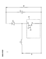
図1は、実施の形態1に係る昇圧チョッパ回路1の構成例を示すブロック図である。図1において、昇圧チョッパ回路1は、スイッチング素子である半導体スイッチ14を有する電流駆動型スイッチング回路10と、インダクタL1と、ダイオードD1と、キャパシタC1とを備える。
(Embodiment 1)
FIG. 1 is a block diagram showing a configuration example of the step-up
図1において、入力電圧ViはインダクタL1を介してダイオードD1のアノード及び半導体スイッチ14のドレインの接続点に印加される。半導体スイッチ14のソースは接地される。ダイオードD1のカソードは出力電圧Voを出力するキャパシタC1の一端に接続され、その他端は接地される。
In FIG. 1, the input voltage Vi is applied to the connection point between the anode of the diode D1 and the drain of the
以上のように構成された昇圧チョッパ回路1において、インダクタL1は電流の変化を妨げる向きに起電力を生じる。従って、半導体スイッチ14がオンからオフに切り替わるとき、インダクタL1はダイオードD1の抵抗により電流が低下するのを妨げるように、入力電圧Viと同じ向きの起電力を生じる。これにより入力電圧Viよりも高い電圧が生じ、当該電圧はキャパシタC1により平滑化され、出力電圧Voに変換される。従って、半導体スイッチ14のオンオフを周期的に選択的に切り替えることで、昇圧チョッパ回路1は、入力電圧Viを、入力電圧Viよりも高圧の直流出力電圧Voに変換して出力する。
In the
図2は、図1の電流駆動型スイッチング回路10の詳細構成例を示すブロック図である。図2において、電流駆動型スイッチング回路10は、過電流保護回路11と、制御部12と、駆動部13と、半導体スイッチ14と、抵抗R1とを備える。過電流保護回路11は、トランジスタQ1,Q2と、プルアップ抵抗R2と、電圧検出回路15とを備える。
FIG. 2 is a block diagram showing a detailed configuration example of the current-driven
図2において、制御部12は、パルス信号である駆動信号Sdrvで駆動部13を制御する。また、制御部12は、過電流保護回路11の電圧検出回路15から入力された検出電圧Vocpを示す信号を監視し、検出電圧Vocpが所定のしきい値未満となったとき、異常検出フラグFhをハイレベルにし、駆動信号Sdrvをローレベルに固定して、駆動部13を停止させる。
In FIG. 2, the
駆動部13は、制御部12からの駆動信号Sdrvに基づいて、抵抗R1を介して半導体スイッチ14のゲートにゲート・ソース間電圧Vgsを印加し、半導体スイッチ14をオンオフ制御する。半導体スイッチ14は例えばGaNデバイス等のスイッチング素子であり、駆動部13によりオンオフ制御されてドレイン電流Idを導通するか否かを選択的に切り替える。なお、ゲート・ソース間電圧Vgsは本発明の「制御電圧」の一例である。
Based on the drive signal Sdrv from the
過電流保護回路11において、トランジスタQ1は、例えばPNP型バイポーラトランジスタである。また、トランジスタQ2は、例えばNPN型バイポーラトランジスタであり、トランジスタQ1のコレクタに接続されたベースと、トランジスタQ1のベースに接続されたコレクタと、接地されたエミッタを有する。また、トランジスタQ2のコレクタは、プルアップ抵抗R2を介してしきい値電圧VTHにプルアップされる。しきい値電圧VTHは、本発明の「プルアップ電圧」の一例である。 In the overcurrent protection circuit 11, the transistor Q1 is, for example, a PNP type bipolar transistor. Further, the transistor Q2 is, for example, an NPN type bipolar transistor, and has a base connected to the collector of the transistor Q1, a collector connected to the base of the transistor Q1, and a grounded emitter. Further, the collector of the transistor Q2 is pulled up to the threshold voltage VTH via the pull-up resistor R2. The threshold voltage VTH is an example of the "pull-up voltage" of the present invention.
ここで、トランジスタQ1がオフ(絶縁)の間、トランジスタQ2のベースに電流は流れない。トランジスタQ1がオンになると、エミッタ・コレクタ間が導通するため、トランジスタQ2のベース・エミッタ間を電流が流れる。従って、トランジスタQ1がオンになると、トランジスタQ2もオンになる。電圧検出回路15は、トランジスタQ2のコレクタ・エミッタ間電圧である検出電圧Vocpを検出して、検出電圧Vocpを示す信号を制御部12に出力する。なお、電圧検出回路15は本発明の「電圧検出部」の一例であり、検出電圧Vocpを示す信号は本発明の「第1の制御信号」の一例である。
Here, no current flows through the base of the transistor Q2 while the transistor Q1 is off (insulated). When the transistor Q1 is turned on, the emitter and collector are electrically connected, so that a current flows between the base and the emitter of the transistor Q2. Therefore, when the transistor Q1 is turned on, the transistor Q2 is also turned on. The
図3は、図1の電流駆動型スイッチング回路10における信号等の動作波形を示すタイミングチャートである。
FIG. 3 is a timing chart showing operation waveforms of signals and the like in the current-driven
図3において、時刻t0において電流駆動型スイッチング回路10が動作を開始し、時刻t1において半導体スイッチ14に短絡が発生した後、時刻t2において制御部12が短絡を検出する。ここで、時刻t0〜t1の期間を定常期間Pnといい、時刻t1〜t2の期間を短絡期間Psといい、時刻t2以降の期間を停止期間Phという。
In FIG. 3, the current-driven
定常期間Pnにおいて、検出電圧Vocpがオーバーシュートする期間(詳細後述)を除いて、プルアップ抵抗R2に電流は流れないため、検出電圧Vocpはしきい値電圧VTHである。このしきい値電圧VTHは、駆動信号Sdrvがハイレベルの時に駆動部13が供給するゲート・ソース間電圧Vgsよりも高く設定されているため、トランジスタQ1及びQ2の両方は定常期間Pnにおいて常にオフである。
Since no current flows through the pull-up resistor R2 except for the period during which the detection voltage Vocp overshoots in the steady period Pn (details will be described later), the detection voltage Vocp is the threshold voltage VTH. Since this threshold voltage VTH is set higher than the gate-source voltage Vgs supplied by the
一般に半導体デバイスを過電流が流れる場合、半導体デバイスに含まれる半導体スイッチのゲート・ソース間電圧がオーバーシュート(瞬間的に上昇)する。本実施の形態においても、図3の時刻t1において、半導体スイッチ14に流れるドレイン電流Idが過剰に上昇するとともに、半導体スイッチ14のゲート・ソース間電圧Vgsは急激に上昇し、しきい値電圧VTHよりも高い値になる。これにより、トランジスタQ1がオンになり、従ってトランジスタQ2もオンになる。
Generally, when an overcurrent flows through a semiconductor device, the gate-source voltage of the semiconductor switch included in the semiconductor device overshoots (instantaneously rises). Also in the present embodiment, at the time t1 of FIG. 3, the drain current Id flowing through the
ここで、トランジスタQ1及びQ2の両方がオンになると、半導体スイッチ14のゲートはトランジスタQ1及びQ2を通じて接地される。従って、ゲート・ソース間電圧Vgsは急速に低下して0となる。これにより半導体スイッチ14はオフになるため、半導体スイッチ14に流れる過電流を停止させ、過電流保護回路11は保護動作を開始することができる。時刻t1で短絡が発生してから、過電流保護回路11が保護動作を開始するまでの時間は、トランジスタQ1,Q2のスイッチングにおける遅延を含み、例えば20〜100ナノ秒程度に短い。
Here, when both the transistors Q1 and Q2 are turned on, the gate of the
また、トランジスタQ2がオンされているとき、検出電圧Vocpは急速に低下して0となる。ここで、抵抗R1がプルアップ抵抗R2よりも小さい場合、ゲート・ソース間電圧Vgsは検出電圧Vocpよりも速く低下する。従って、ゲート・ソース間電圧Vgsが低下しても、トランジスタQ1をオンのままに保つことができる。その後、制御部の駆動信号Sdrvがローレベルとなると、駆動部13は停止され、ゲート・ソース間電圧Vgsが0に低下する。従ってトランジスタQ1,Q2は順次オフになるため、検出電圧Vocpは再度しきい値電圧VTHまで上昇し、保護動作が終了する。
Further, when the transistor Q2 is turned on, the detection voltage Vocp rapidly decreases to 0. Here, when the resistor R1 is smaller than the pull-up resistor R2, the gate-source voltage Vgs drops faster than the detected voltage Vocp. Therefore, the transistor Q1 can be kept on even if the gate-source voltage Vgs drops. After that, when the drive signal Sdrv of the control unit becomes low level, the
電圧検出回路15は、検出電圧Vocpを示す信号を制御部12に出力している。制御部12は検出電圧Vocpの値を監視し、検出電圧Vocpが所定のしきい値未満になると、保護動作が行われたと判断して異常検出フラグFhをハイレベルにし、駆動信号Sdrvの出力を停止させる(時刻t2)。停止期間Phでは、駆動信号Sdrvは常にローレベルであり、半導体スイッチ14は常にオフのままである。
The
ここで、制御部12の応答が遅い場合、時刻t2において駆動信号Sdrvの出力が停止する前に、再度駆動信号Sdrvがハイレベルになり得る。その場合には図3に示すように、半導体スイッチ14に再度過電流が流れ、過電流保護回路11は再度保護動作を開始する。
Here, when the response of the
以上のように、本実施の形態に係る過電流保護回路11は、プルアップ抵抗R2と、PNP型であるトランジスタQ1と、NPN型であるトランジスタQ2と、電圧検出回路15とを備える。半導体スイッチ14のゲート・ソース間電圧Vgsがしきい値電圧VTHを上回ると、トランジスタQ1,Q2は順次オンになる。これにより過電流保護回路11は、ゲート・ソース間電圧Vgsを0まで低下させて、半導体スイッチをオフする保護動作を開始する。また、制御部12は電圧検出回路15により検出された検出電圧Vocpを監視して、検出電圧Vocpが所定のしきい値電圧未満になると、駆動部13を停止させて半導体スイッチ14をオフする。従って本実施の形態によれば、半導体スイッチ14に流れる過電流を、従来技術に比較して高速に停止させ、半導体スイッチ14を保護することができる。
As described above, the overcurrent protection circuit 11 according to the present embodiment includes a pull-up resistor R2, a PNP type transistor Q1, an NPN type transistor Q2, and a
(実施の形態2)
実施の形態1では、半導体スイッチ14のゲート・ソース間電圧Vgsが立ち上がる時、図3に示したように検出電圧Vocpがオーバーシュートする。これは検出電圧Vocpの低下を遅らせ、保護動作の開始を遅延させる原因となる。また先述の通り、短絡期間Psにおける過電流保護の後、制御部12の応答速度が遅い場合、半導体スイッチ14に繰り返し過電流が流れるため、これは望ましくない。
(Embodiment 2)
In the first embodiment, when the gate-source voltage Vgs of the
図4は、実施の形態2に係る電流駆動型スイッチング回路10Aの構成例を示すブロック図である。図4において、電流駆動型スイッチング回路10Aは、電流駆動型スイッチング回路10と比較して以下の点で異なる。
(1)過電流保護回路11Aはさらに、トランジスタQ2のコレクタ及びエミッタに接続されたキャパシタCaを備える。
(2)しきい値電圧VTHの電源はプルアップ抵抗R2を介して、キャパシタCaをしきい値電圧VTHまで充電する。
FIG. 4 is a block diagram showing a configuration example of the current-driven
(1) The overcurrent protection circuit 11A further includes a capacitor Ca connected to a collector and an emitter of the transistor Q2.
(2) The power supply of the threshold voltage VTH charges the capacitor Ca to the threshold voltage VTH via the pull-up resistor R2.
図5は、図4の電流駆動型スイッチング回路10Aにおける信号等の動作波形を示すタイミングチャートである。時刻t11は、図3の短絡期間Psにおいて再度駆動信号Sdrvが立ち上がるタイミングを示す。
FIG. 5 is a timing chart showing operation waveforms of signals and the like in the current-driven
図5において、時刻t1では半導体スイッチ14に短絡が発生し、ゲート・ソース間電圧Vgsが急激に立ち上がる。この時、ゲート・ソース間電圧Vgsの立ち上がりにより検出電圧Vocpがオーバーシュートするが、この変化はキャパシタCaにより軽減される。従って、保護動作の開始の遅延を抑えることができる。
In FIG. 5, at time t1, a short circuit occurs in the
また、短絡期間Ps1においてトランジスタQ1,Q2がオンになると、キャパシタCaはトランジスタQ2を介して接地され、キャパシタCaはゼロ電位まで放電する。その後、駆動信号Sdrvがローレベルとなり、トランジスタQ1,Q2がオフになって検出電圧Vocpが上昇し始める。ここで、しきい値電圧VTHはキャパシタCaを充電する。従って、検出電圧Vocpがしきい値電圧VTHまで上昇するのにかかる時間は、実施の形態1における当該時間よりも長くなる。キャパシタCaを適切に選択することで、検出電圧Vocpがしきい値電圧VTHまで上昇するのにかかる時間を、再度駆動信号Sdrvがハイレベルになる(時刻t11)までの時間よりも長くすることができる。これにより、再度制御信号がハイレベルになっても、ゲート・ソース間電圧Vgsがしきい値電圧VTHに達する前にトランジスタQ1,Q2はオンになり、半導体スイッチ14は保護される。
When the transistors Q1 and Q2 are turned on during the short-circuit period Ps1, the capacitor Ca is grounded via the transistor Q2, and the capacitor Ca is discharged to zero potential. After that, the drive signal Sdrv becomes low level, the transistors Q1 and Q2 are turned off, and the detection voltage Vocp begins to rise. Here, the threshold voltage VTH charges the capacitor Ca. Therefore, the time required for the detection voltage Vocp to rise to the threshold voltage VTH is longer than the time in the first embodiment. By properly selecting the capacitor Ca, the time required for the detected voltage Vocp to rise to the threshold voltage VTH can be made longer than the time required for the drive signal Sdrv to reach a high level again (time t11). can. As a result, even if the control signal becomes high level again, the transistors Q1 and Q2 are turned on before the gate-source voltage Vgs reaches the threshold voltage VTH, and the
以上のように、本実施の形態に係る過電流保護回路11Aは、過電流保護回路11に加えてさらにキャパシタCaを備える。これにより、過電流保護回路11Aが保護動作を行った後、当該保護動作から復帰するまでの時間を、図2の過電流保護回路11よりも長くし、半導体スイッチ14に過電流が繰り返し流れる現象を防ぐことができる。また、ゲート・ソース間電圧Vgsの立ち上がりによる検出電圧Vocpのオーバーシュートを図2の過電流保護回路11よりも小さくし、保護動作の開始における遅延を過電流保護回路11よりも低減することができる。
As described above, the overcurrent protection circuit 11A according to the present embodiment further includes a capacitor Ca in addition to the overcurrent protection circuit 11. As a result, after the overcurrent protection circuit 11A performs the protection operation, the time from the protection operation to the recovery is made longer than that of the overcurrent protection circuit 11 of FIG. 2, and the overcurrent repeatedly flows through the
(実施の形態3)
図6は、実施の形態3に係る電流駆動型スイッチング回路10Bの構成例を示すブロック図である。
(Embodiment 3)
FIG. 6 is a block diagram showing a configuration example of the current-driven
図6において、電流駆動型スイッチング回路10Bは、電流駆動型スイッチング回路10Aと比較して以下の点で異なる。
(1)さらに抵抗R3及びキャパシタCbを含む時定数回路18を備える。
(2)時定数回路18は、トランジスタQ2のコレクタ及びエミッタに並列に接続される。
In FIG. 6, the current-driven
(1) Further, a time
(2) The time
これにより、ゼロ電位まで放電したキャパシタCaがしきい値電圧VTHまで充電される時定数は調整され、過電流保護回路11Bが保護動作から復帰するまでの時間は、過電流保護回路11Aよりも長くなる。なお、実施の形態1の電流駆動型スイッチング回路10にも、時定数回路18を挿入して同様の効果を得られる。
As a result, the time constant at which the capacitor Ca discharged to zero potential is charged to the threshold voltage VTH is adjusted, and the time until the
以上のように、実施の形態3に係る電流駆動型スイッチング回路10Bはさらに、抵抗R3とキャパシタCbとを含む時定数回路18を備える。過電流保護回路11Bが保護動作から復帰するまでの時間は、抵抗R3及びキャパシタCbを適切に選択することで調整される。
As described above, the current-driven
(実施の形態4)
図7は、実施の形態4に係る電流駆動型スイッチング回路10Cの構成例を示すブロック図である。図7において、電流駆動型スイッチング回路10Cは図6の電流駆動型スイッチング回路10Bと比較して以下の点で異なる。
(1)過電流保護回路11Cはさらに、アノードが抵抗R3の低電位側の一端に接続され、カソードが抵抗R3の他端に接続されたダイオードD2を備える。
(Embodiment 4)
FIG. 7 is a block diagram showing a configuration example of the current-driven
(1) The overcurrent protection circuit 11C further includes a diode D2 in which the anode is connected to one end of the resistor R3 on the low potential side and the cathode is connected to the other end of the resistor R3.
以上のように、実施の形態4に係る電流駆動型スイッチング回路10Cはさらに、ダイオードD2を備える。ゲート・ソース間電圧Vgs等におけるノイズが過電流保護回路11Cに与える影響は、過電流保護回路11Bよりも抑えられる。
As described above, the current-driven
(実施の形態5)
図8は、実施の形態5に係る電流駆動型スイッチング回路10Dの構成例を示すブロック図である。
(Embodiment 5)
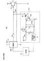
FIG. 8 is a block diagram showing a configuration example of the current-driven
図8において、電流駆動型スイッチング回路10Dは、図6の電流駆動型スイッチング回路10Bと比較して以下の点で異なる。
(1)電流駆動型スイッチング回路10Dはさらに、MOS駆動部16を備える。
(2)抵抗R3をMOSFET17で置き換える。
In FIG. 8, the current-driven
(1) The current drive
(2) The resistor R3 is replaced with the
図8において、MOS駆動部16は、制御部12により制御されて、MOS駆動信号Smを出力してMOSFET17をオンオフ制御する。MOSFET17はMOS駆動信号Smにより制御され、MOS駆動信号Smがローレベルを有する期間ではしきい値電圧VTHを遮断(オフ)する。
In FIG. 8, the
図9は図8の電流駆動型スイッチング回路10Dにおける信号等の動作波形の例を示すタイミングチャートである。
FIG. 9 is a timing chart showing an example of an operation waveform of a signal or the like in the current-driven
図9において、電流駆動型スイッチング回路10Dは動作の開始(時刻t0)よりも前に準備期間Pp1(時刻t21〜t22)を有する。時刻t21において、制御部12はMOS駆動部16を介してMOSFET17をオンにする。キャパシタCaがしきい値電圧VTHまで充電された後、制御部12はMOS駆動部16を介してMOSFET17をオフする(時刻t22)。
In FIG. 9, the current-driven
その後、時刻t0〜t1の定常期間Pn1における通常の動作の後、短絡期間Ps1において保護が開始され、キャパシタCaはゼロ電位まで放電する。実施の形態1〜4ではこの後、駆動信号SdrvがローレベルになってトランジスタQ1,Q2がオフになり、キャパシタCaが再度充電された。しかしながら本実施の形態では、MOSFET17がオフされているため、キャパシタCaは充電されず、過電流保護回路11Dは保護動作を保持する。その後、制御部12は検出電圧Vocpが所定のしきい値電圧未満になると、異常検出フラグFhをハイレベルにして駆動信号Sdrvの出力を停止する(時刻t2)。
Then, after normal operation in the steady period Pn1 at times t0 to t1, protection is started in the short-circuit period Ps1 and the capacitor Ca is discharged to zero potential. In the first to fourth embodiments, after that, the drive signal Sdrv becomes low level, the transistors Q1 and Q2 are turned off, and the capacitor Ca is charged again. However, in the present embodiment, since the
時刻t2〜t23の期間は停止期間Phである。停止期間Phにおいて、昇圧チョッパ回路1の使用者は、短絡箇所を修理して、短絡を解消することができる。その後、例えば上位の制御回路が短絡の解消を検出して制御部12を制御するか、又は使用者が直接制御部12を操作することで、制御部12の異常検出フラグFhはローレベルになる(時刻t23)。制御部12は異常検出フラグFhがローレベルになったのを検出して、再度キャパシタCaを充電するためにMOSFET17をオンする(時刻t24)。時刻t24〜t25は、2回目の準備期間Pp2である。準備期間Pp1と同様、準備期間Pp2においてMOS駆動信号Smはハイレベルを有し、キャパシタCaはしきい値電圧VTHまで充電される。
The period from time t2 to t23 is the stop period Ph. During the stop period Ph, the user of the
準備期間Pp2におけるキャパシタCaの十分な充電により、過電流保護回路11Dは保護動作から復帰する。その後、電流駆動型スイッチング回路10Bは定常期間Pn2において、定常期間Pn1と同様の正常な動作を再開する(時刻t25)。
With sufficient charging of the capacitor Ca in the preparation period Pp2, the
以上のように、実施の形態5に係る電流駆動型スイッチング回路10Dは、MOS駆動部16と、MOSFET17とを備える。MOSFET17はMOS駆動部16を介して制御部12により制御され、しきい値電圧VTHをオンオフ制御する。検出電圧Vocpは、MOSFET17がオフの期間では上昇しないため、制御部12の応答の遅延等にかかわらず、保護動作からの復帰を任意のタイミングで行うことができる。なお、MOSFET17が寄生ダイオードを含む場合、実施の形態4に係る電流駆動型スイッチング回路10Cと同様、ノイズを抑える効果が得られる。なお、本実施の形態に係るMOSFET17は、実施の形態1〜4の電流駆動型スイッチング回路10,10A〜10Cのいずれにも同様に挿入可能であり、同様の効果が得られる。また、本実施の形態に係るMOSFET17は、本発明の「別のスイッチング素子」の一例である。
As described above, the current drive
(実施の形態6)
図10は、実施の形態6に係る電流駆動型スイッチング回路10Eの構成例を示すブロック図である。図10において、電流駆動型スイッチング回路10Eは図8の電流駆動型スイッチング回路10Dと比較して、以下の点が異なる。
(1)MOSFET17に代えてトランジスタ17aを備える。
(2)MOS駆動部16に代えてトランジスタ駆動部16aを備える。
(Embodiment 6)
FIG. 10 is a block diagram showing a configuration example of the current-driven
(1) A
(2) A
制御部12は、トランジスタ駆動部16aを介してトランジスタ17aのベース電流Itrを制御することで、トランジスタ17aをオンオフ制御する。これにより、実施の形態5と同様の効果が得られる。なお、本実施の形態におけるトランジスタ17aは、本発明の「別のスイッチング素子」の一例である。
The
(変形例)
以上、本発明の実施の形態を詳細に説明してきたが、前述までの説明はあらゆる点において本発明の例示に過ぎない。本発明の範囲を逸脱することなく種々の改良や変形を行うことができることは言うまでもない。例えば、以下のような変更が可能である。なお、以下では、上記実施の形態と同様の構成要素に関しては同様の符号を用い、上記実施の形態と同様の点については、適宜説明を省略した。以下の変形例は適宜組み合わせ可能である。
(Modification example)
Although the embodiments of the present invention have been described in detail above, the above description is merely an example of the present invention in all respects. Needless to say, various improvements and modifications can be made without departing from the scope of the present invention. For example, the following changes can be made. In the following, the same reference numerals will be used for the same components as those in the above embodiment, and the same points as in the above embodiment will be omitted as appropriate. The following modifications can be combined as appropriate.
実施の形態1〜3では、本発明に係る電流駆動型スイッチング回路10,10A〜10Eを備える半導体デバイスとして、昇圧チョッパ回路1を説明した。しかしながら、本発明はこれに限らず、半導体スイッチで電流をスイッチング制御する回路及び装置等に利用可能である。
In the first to third embodiments, the step-up
例えば、図11は、変形例1に係るハーフブリッジインバータ回路1Aの構成例を示すブロック図である。図11において、ハーフブリッジインバータ回路1Aは、インダクタL2と、2個の電流駆動型スイッチング回路10と、キャパシタC2とを備える。
For example, FIG. 11 is a block diagram showing a configuration example of the half-
図11において、2個の電流駆動型スイッチング回路10の半導体スイッチ14は、周期的に交互にオンするよう制御される。これにより入力電圧Viはスイッチングされ、キャパシタC2により平滑化されて、交流出力電圧Voに変換される。これによりハーフブリッジインバータ回路1Aは、直流の入力電圧Viをスイッチングし、交流の出力電圧Voに変換して出力する。2個の電流駆動型スイッチング回路10は、それぞれ電流駆動型スイッチング回路10A〜10Eのいずれか1つで置き換えられてもよい。
In FIG. 11, the semiconductor switches 14 of the two current-driven
また、図12は、変形例2に係るフルブリッジインバータ回路1Bの構成例を示すブロック図である。図12において、フルブリッジインバータ回路1Bは、キャパシタC3と、4個の電流駆動型スイッチング回路10と、インダクタL3,L4とを備える。
Further, FIG. 12 is a block diagram showing a configuration example of the full
図12において、4個の電流駆動型スイッチング回路10は、第1及び第4の電流駆動型スイッチング回路10(図左上及び右下)がオンであり、かつ第2及び第3の電流駆動型スイッチング回路10(図左下及び右上)がオフである期間と、これらのオンオフを逆転させた期間とが、周期的に交互に現れるよう制御される。これにより入力電圧Viはスイッチングされ、スイッチングされた入力電圧Viは、キャパシタC3及びインダクタL3,L4により平滑化される。これによりフルブリッジインバータ回路1Bは、直流の入力電圧Viをスイッチングし、交流の出力電圧Voに変換して出力する。4個の電流駆動型スイッチング回路10は、それぞれ電流駆動型スイッチング回路10A〜10Eのいずれか1つで置き換えられてもよい。
In FIG. 12, in the four current-driven
このように、本発明に係る電流駆動型スイッチング回路及び過電流保護回路は、半導体デバイスで電流をスイッチング制御する回路及び装置に利用可能である。 As described above, the current-driven switching circuit and the overcurrent protection circuit according to the present invention can be used in circuits and devices for switching and controlling current in semiconductor devices.
また、実施の形態1〜6では、しきい値電圧VTHの電源からの電流を制限する手段としてプルアップ抵抗R2を用いた。しかしながら、本発明はこれに限らず、プルアップ抵抗R2に代えてダイオード等を用いてもよい。さらに、実施の形態1〜6では、スイッチング回路として電流駆動型スイッチング回路10,10A〜10Eを用いた。しかしながら、本発明はこれに限らず、電流駆動型スイッチング回路に代えて電圧駆動型スイッチング回路を用いてもよい。
Further, in the first to sixth embodiments, the pull-up resistor R2 is used as a means for limiting the current from the power source of the threshold voltage VTH. However, the present invention is not limited to this, and a diode or the like may be used instead of the pull-up resistor R2. Further, in the first to sixth embodiments, the current drive
1 昇圧チョッパ回路
1A ハーフブリッジインバータ回路
1B フルブリッジインバータ回路
10,10A〜10E 電流駆動型スイッチング回路
11,11A〜11E 過電流保護回路
12 制御部
13 駆動部
14 半導体スイッチ
15 電圧検出回路
16 MOS駆動部
16a トランジスタ駆動部
17 MOSFET
17a トランジスタ
18 時定数回路
Q1,Q2 トランジスタ
R1,R2 抵抗
1 Boost
Claims (7)
PNP型バイポーラトランジスタであって、前記制御電圧に接続されたエミッタを有する第1のトランジスタと、
NPN型バイポーラトランジスタであって、前記第1のトランジスタのコレクタに接続されたベースと、前記第1のトランジスタのベースに接続されかつ所定のプルアップ電圧にプルアップされたコレクタと、接地されたエミッタとを有する第2のトランジスタとを備え、
前記過電流保護回路は、前記制御電圧が所定の第1のしきい値電圧を超えるとき、前記第1及び第2のトランジスタがオンされ、前記プルアップ電圧の低下により前記制御電圧が低下されて、前記スイッチング素子をオフする保護動作を開始する、
過電流保護回路。 In an overcurrent protection circuit for switching elements that are on / off controlled based on the control voltage
A PNP type bipolar transistor, the first transistor having an emitter connected to the control voltage, and
An NPN type bipolar transistor having a base connected to the collector of the first transistor, a collector connected to the base of the first transistor and pulled up to a predetermined pull-up voltage, and a grounded emitter. With a second transistor with and
In the overcurrent protection circuit, when the control voltage exceeds a predetermined first threshold voltage, the first and second transistors are turned on, and the control voltage is lowered due to the drop in the pull-up voltage. , Start the protection operation to turn off the switching element,
Overcurrent protection circuit.
請求項1に記載の過電流保護回路。 A capacitor connected to a collector and an emitter of the second transistor, further comprising a first capacitor that reduces a change in the pull-up voltage when the control voltage rises.
The overcurrent protection circuit according to claim 1.
請求項1又は2に記載の過電流保護回路。 A time constant circuit connected in parallel to the collector and emitter of the second transistor, including a resistor and a second capacitor, and by changing the time constant, the time from the start to the end of the protection operation. Further equipped with a time constant circuit to adjust
The overcurrent protection circuit according to claim 1 or 2.
請求項3に記載の過電流保護回路。 Further comprising a diode connected in parallel with the resistor.
The overcurrent protection circuit according to claim 3.
前記プルアップ電圧を検出して、当該検出した検出電圧を、前記スイッチング素子をオフするための第1の制御信号として前記制御部に出力する電圧検出部とをさらに備える、
請求項1〜4のうちのいずれか1つに記載の過電流保護回路。 The control unit that generates the control voltage and
A voltage detection unit that detects the pull-up voltage and outputs the detected detection voltage to the control unit as a first control signal for turning off the switching element is further provided.
The overcurrent protection circuit according to any one of claims 1 to 4.
請求項5に記載の過電流保護回路。 It further comprises another switching element that turns the pull-up voltage from off to on based on a second control signal from the control when the overcurrent protection circuit returns from the protection operation.
The overcurrent protection circuit according to claim 5.
前記スイッチング素子とを備える、
スイッチング回路。 The overcurrent protection circuit according to any one of claims 1 to 6.
The switching element is provided.
Switching circuit.
Priority Applications (5)
| Application Number | Priority Date | Filing Date | Title |
|---|---|---|---|
| JP2019017332A JP6965902B2 (en) | 2019-02-01 | 2019-02-01 | Overcurrent protection circuit and switching circuit |
| PCT/JP2020/003398 WO2020158853A1 (en) | 2019-02-01 | 2020-01-30 | Overcurrent protection circuit and switching circuit |
| CN202080004940.1A CN112640279A (en) | 2019-02-01 | 2020-01-30 | Overcurrent protection circuit and switching circuit |
| EP20749654.8A EP3832866A4 (en) | 2019-02-01 | 2020-01-30 | Overcurrent protection circuit and switching circuit |
| US17/273,101 US11545972B2 (en) | 2019-02-01 | 2020-01-30 | Overcurrent protection circuit for switching element turned on and off based on control voltage |
Applications Claiming Priority (1)
| Application Number | Priority Date | Filing Date | Title |
|---|---|---|---|
| JP2019017332A JP6965902B2 (en) | 2019-02-01 | 2019-02-01 | Overcurrent protection circuit and switching circuit |
Publications (3)
| Publication Number | Publication Date |
|---|---|
| JP2020127267A JP2020127267A (en) | 2020-08-20 |
| JP2020127267A5 JP2020127267A5 (en) | 2021-04-22 |
| JP6965902B2 true JP6965902B2 (en) | 2021-11-10 |
Family
ID=71841854
Family Applications (1)
| Application Number | Title | Priority Date | Filing Date |
|---|---|---|---|
| JP2019017332A Active JP6965902B2 (en) | 2019-02-01 | 2019-02-01 | Overcurrent protection circuit and switching circuit |
Country Status (5)
| Country | Link |
|---|---|
| US (1) | US11545972B2 (en) |
| EP (1) | EP3832866A4 (en) |
| JP (1) | JP6965902B2 (en) |
| CN (1) | CN112640279A (en) |
| WO (1) | WO2020158853A1 (en) |
Families Citing this family (3)
| Publication number | Priority date | Publication date | Assignee | Title |
|---|---|---|---|---|
| JP7404666B2 (en) * | 2019-06-11 | 2023-12-26 | 富士電機株式会社 | Integrated circuits, power supply circuits |
| JP2022041671A (en) * | 2020-09-01 | 2022-03-11 | オムロン株式会社 | Overcurrent protection circuit and switching circuit |
| CN112636733A (en) * | 2020-12-07 | 2021-04-09 | 珠海格力电器股份有限公司 | IGBT drive circuit and power conversion equipment |
Family Cites Families (10)
| Publication number | Priority date | Publication date | Assignee | Title |
|---|---|---|---|---|
| JP2000037073A (en) * | 1998-07-15 | 2000-02-02 | Yaskawa Electric Corp | Dc/dc converter |
| US6825504B2 (en) * | 1999-05-03 | 2004-11-30 | Hitachi, Ltd. | Semiconductor integrated circuit device and method of manufacturing the same |
| US7548401B2 (en) * | 2001-03-16 | 2009-06-16 | Sarnoff Corporation | Electrostatic discharge protection structures for high speed technologies with mixed and ultra-low voltage supplies |
| KR100828247B1 (en) * | 2003-12-26 | 2008-05-07 | 로무 가부시키가이샤 | Overcurrent protection circuit, motor drive circuit, and semiconductor device |
| JP2006014402A (en) | 2004-06-22 | 2006-01-12 | Toshiba Mitsubishi-Electric Industrial System Corp | Overcurrent protector of power converter |
| WO2010150488A1 (en) * | 2009-06-24 | 2010-12-29 | パナソニック株式会社 | Power supply protection circuit and motor drive device provided with same |
| JP2015136234A (en) * | 2014-01-17 | 2015-07-27 | セイコーエプソン株式会社 | Short-circuit protection circuit, power circuit and power supply unit |
| WO2016114416A1 (en) * | 2015-01-13 | 2016-07-21 | 주식회사 실리콘웍스 | Inductive load driving circuit including balancing circuit for clamping circuit and control method therefor |
| JP2018129761A (en) * | 2017-02-10 | 2018-08-16 | 株式会社オートネットワーク技術研究所 | Switch control device |
| JP6959096B2 (en) * | 2017-10-13 | 2021-11-02 | エイブリック株式会社 | Charge / discharge control circuit and battery device equipped with this |
-
2019
- 2019-02-01 JP JP2019017332A patent/JP6965902B2/en active Active
-
2020
- 2020-01-30 US US17/273,101 patent/US11545972B2/en active Active
- 2020-01-30 WO PCT/JP2020/003398 patent/WO2020158853A1/en unknown
- 2020-01-30 EP EP20749654.8A patent/EP3832866A4/en active Pending
- 2020-01-30 CN CN202080004940.1A patent/CN112640279A/en active Pending
Also Published As
| Publication number | Publication date |
|---|---|
| EP3832866A1 (en) | 2021-06-09 |
| US11545972B2 (en) | 2023-01-03 |
| WO2020158853A1 (en) | 2020-08-06 |
| US20210226620A1 (en) | 2021-07-22 |
| EP3832866A4 (en) | 2022-04-13 |
| CN112640279A (en) | 2021-04-09 |
| JP2020127267A (en) | 2020-08-20 |
Similar Documents
| Publication | Publication Date | Title |
|---|---|---|
| JP6170119B2 (en) | System and method for driving a power switch | |
| JP5571594B2 (en) | Switching power supply | |
| US11070046B2 (en) | Short-circuit protection circuit for self-arc-extinguishing type semiconductor element | |
| US7315439B2 (en) | Method and circuit arrangement for limiting an overvoltage | |
| JP6965902B2 (en) | Overcurrent protection circuit and switching circuit | |
| JP2007336694A (en) | Drive circuit for insulated-gate semiconductor device | |
| JP6417546B2 (en) | Gate drive circuit and power converter using the same | |
| US10243551B1 (en) | Over voltage protection for cascode switching power device | |
| JP4779549B2 (en) | A gate driving circuit of a voltage driven semiconductor element. | |
| JP2021013259A (en) | Gate drive device and power conversion device | |
| CN102005731A (en) | Controller, power converter and method for providing over-temperature protection | |
| US10536088B2 (en) | Switched mode power supply controller | |
| JP4321491B2 (en) | Voltage-driven semiconductor device driving apparatus | |
| JP2006352931A (en) | Switching element protection circuit | |
| JP2009095214A (en) | Dc-dc converter circuit | |
| JP7205636B2 (en) | Overcurrent protection circuit and switching circuit | |
| JP5069259B2 (en) | Semiconductor circuit device | |
| WO2022050040A1 (en) | Overcurrent protection circuit, and switching circuit | |
| JP2010178579A (en) | Semiconductor apparatus | |
| US10075158B2 (en) | Method and drive circuit for driving a transistor | |
| JP2006050776A (en) | Semiconductor switch circuit, power conversion device, inverter device, and air-conditioner | |
| JP6094879B2 (en) | LDMOSFET surge current protection circuit | |
| CN116722717A (en) | Minimum peak current of power converter | |
| JP2018093638A (en) | Protection circuit, and motor unit | |
| JP2004234584A (en) | Power source circuit |
Legal Events
| Date | Code | Title | Description |
|---|---|---|---|
| A621 | Written request for application examination |
Free format text: JAPANESE INTERMEDIATE CODE: A621 Effective date: 20201215 |
|
| A521 | Request for written amendment filed |
Free format text: JAPANESE INTERMEDIATE CODE: A523 Effective date: 20210308 |
|
| TRDD | Decision of grant or rejection written | ||
| A01 | Written decision to grant a patent or to grant a registration (utility model) |
Free format text: JAPANESE INTERMEDIATE CODE: A01 Effective date: 20210921 |
|
| A61 | First payment of annual fees (during grant procedure) |
Free format text: JAPANESE INTERMEDIATE CODE: A61 Effective date: 20211004 |
|
| R150 | Certificate of patent or registration of utility model |
Ref document number: 6965902 Country of ref document: JP Free format text: JAPANESE INTERMEDIATE CODE: R150 |