JP6950488B2 - 3-level power converter - Google Patents
3-level power converter Download PDFInfo
- Publication number
- JP6950488B2 JP6950488B2 JP2017224683A JP2017224683A JP6950488B2 JP 6950488 B2 JP6950488 B2 JP 6950488B2 JP 2017224683 A JP2017224683 A JP 2017224683A JP 2017224683 A JP2017224683 A JP 2017224683A JP 6950488 B2 JP6950488 B2 JP 6950488B2
- Authority
- JP
- Japan
- Prior art keywords
- semiconductor switching
- switching element
- terminal side
- wiring
- side board
- Prior art date
- Legal status (The legal status is an assumption and is not a legal conclusion. Google has not performed a legal analysis and makes no representation as to the accuracy of the status listed.)
- Expired - Fee Related
Links
Images


Landscapes
- Inverter Devices (AREA)
Description
この発明は、3レベル電力変換装置に関し、特に、多層配線基板上に複数の半導体スイッチング素子が実装される3レベル電力変換装置に関する。 The present invention relates to a three-level power conversion device, and more particularly to a three-level power conversion device in which a plurality of semiconductor switching elements are mounted on a multilayer wiring substrate.
従来、多層配線基板上に複数の半導体スイッチング素子が実装される3レベル電力変換装置が知られている(たとえば、特許文献1参照)。 Conventionally, a three-level power conversion device in which a plurality of semiconductor switching elements are mounted on a multilayer wiring substrate is known (see, for example, Patent Document 1).
上記特許文献1の3レベル電力変換装置は、直流電源に並列に接続されるとともに、互いに直列に接続された2つの平滑コンデンサを備える。また、この3レベル電力変換装置は、直流電源および平滑コンデンサの各々に並列に接続されるとともに、互いに直列に接続された4つの半導体スイッチング素子を備える。この4つの半導体スイッチング素子の各々は、多層配線基板上に実装される場合がある。この場合、多層配線基板は、4つの半導体スイッチング素子の各々のソース端子に接続され、多層配線基板内に配線されるソース端子側基板配線と、4つの半導体スイッチング素子の各々のドレイン端子に接続され、多層配線基板内に配線されるドレイン端子側基板配線とを含む。また、4つの半導体スイッチング素子の各々の、ソース端子側基板配線とドレイン端子側基板配線との間には、寄生容量が生じる場合がある。
The three-level power converter of
ここで、上記特許文献1に記載されているような従来の3レベル電力変換装置では、4つの半導体スイッチング素子の寄生容量が互いに異なるため、4つの寄生容量の各々に電荷を充電するのに要する時間に差が生じる。この場合、寄生容量の充電時間が互いに異なることに起因して、半導体スイッチング素子のオンオフに要する時間にも互いに差異が生じる。このため、2つの平滑コンデンサの放電(充電)の時間に差が生じる場合がある。この差は、通常は数ns〜十nsレベルのわずかな差である。しかしながら、時間の経過によるスイッチング回数の増加とともに放電(充電)の時間差の影響が2つのコンデンサに蓄積され、2つの平滑コンデンサのうち少なくとも一方の充電電圧が過大になり、平滑コンデンサに並列に接続されているスイッチング素子に過大な電圧が印加されるという問題点がある。
Here, in the conventional three-level power conversion device as described in
この発明は、上記のような課題を解決するためになされたものであり、この発明の1つの目的は、スイッチング素子に過大な電圧が印加されるのを抑制することが可能な3レベル電力変換装置を提供することである。 The present invention has been made to solve the above problems, and one object of the present invention is a three-level power conversion capable of suppressing an excessive voltage from being applied to a switching element. To provide a device.
上記目的を達成するために、この発明の一の局面による3レベル電力変換装置は、直流電源と、直流電源に並列に接続され、互いに直列に接続された複数のコンデンサを含むコンデンサ回路と、コンデンサ回路に並列に接続されるとともに、多層配線基板上において実装され、第1半導体スイッチング素子、第2半導体スイッチング素子、第3半導体スイッチング素子、第4半導体スイッチング素子の順に正電圧側から直列に接続されているスイッチング回路と、を備え、多層配線基板は、第1半導体スイッチング素子、第2半導体スイッチング素子、第3半導体スイッチング素子、および、第4半導体スイッチング素子の各々の、ソース端子に接続されているソース端子側基板配線と、ドレイン端子に接続されているドレイン端子側基板配線とを含み、多層配線基板の実装面に略垂直な方向から見て、第1半導体スイッチング素子、第2半導体スイッチング素子、第3半導体スイッチング素子、および、第4半導体スイッチング素子の各々の、ソース端子側基板配線とドレイン端子側基板配線との重なり具合が調整されている。 In order to achieve the above object, the three-level power converter according to one aspect of the present invention includes a DC power supply, a capacitor circuit including a plurality of capacitors connected in parallel to the DC power supply and connected in series with each other, and a capacitor. It is connected in parallel to the circuit, mounted on a multilayer wiring board, and connected in series from the positive voltage side in the order of the first semiconductor switching element, the second semiconductor switching element, the third semiconductor switching element, and the fourth semiconductor switching element. The multilayer wiring board is connected to the source terminal of each of the first semiconductor switching element, the second semiconductor switching element, the third semiconductor switching element, and the fourth semiconductor switching element. The first semiconductor switching element, the second semiconductor switching element, including the source terminal side board wiring and the drain terminal side board wiring connected to the drain terminal, when viewed from a direction substantially perpendicular to the mounting surface of the multilayer wiring board, The degree of overlap between the source terminal side board wiring and the drain terminal side board wiring of each of the third semiconductor switching element and the fourth semiconductor switching element is adjusted.
ここで、各半導体スイッチング素子の寄生容量の充電に要する時間の長さが互いに異なる場合、各半導体スイッチング素子のオンオフに要する時間にも互いに差異が生じる。このため、第1半導体スイッチング素子および第4半導体スイッチング素子の寄生容量が互いに異なるか、または、第2半導体スイッチング素子および第3半導体スイッチング素子の寄生容量が互いに異なる場合、複数のコンデンサを充放電する時間に差異が生じる。これに対して、この発明の一の局面による3レベル電力変換装置では、ソース端子側基板配線とドレイン端子側基板配線との重なり具合を調整することによって、第1半導体スイッチング素子および第4半導体スイッチング素子の寄生容量を略等しくすることができるとともに、第2半導体スイッチング素子および第3半導体スイッチング素子の寄生容量を略等しくすることができる。これにより、複数のコンデンサを充放電する時間に差が生じるのを抑制することができる。その結果、複数のコンデンサに充電される電圧に差が生じるのを抑制することができるとともに、複数のコンデンサの充電電圧が過大になるのを抑制することができる。これにより、複数のコンデンサに並列に接続されている、第1半導体スイッチング素子、第2半導体スイッチング素子、第3半導体スイッチング素子、および、第4半導体スイッチング素子の各々に過大な電圧が印加されるのを抑制することができる。また、ソース端子側基板配線とドレイン端子側基板配線との重なり具合という可視的なパラメータを調整すればよいので、比較的容易に寄生容量の調整を行うことができる。 Here, when the lengths of time required to charge the parasitic capacitance of each semiconductor switching element are different from each other, the time required to turn on / off each semiconductor switching element also differs from each other. Therefore, when the parasitic capacitances of the first semiconductor switching element and the fourth semiconductor switching element are different from each other, or when the parasitic capacitances of the second semiconductor switching element and the third semiconductor switching element are different from each other, a plurality of capacitors are charged and discharged. There is a difference in time. On the other hand, in the three-level power conversion device according to one aspect of the present invention, the first semiconductor switching element and the fourth semiconductor switching are performed by adjusting the degree of overlap between the source terminal side board wiring and the drain terminal side board wiring. The parasitic capacitances of the elements can be made substantially equal, and the parasitic capacitances of the second semiconductor switching element and the third semiconductor switching element can be made substantially equal. As a result, it is possible to suppress a difference in the charging / discharging time of the plurality of capacitors. As a result, it is possible to suppress a difference in the voltages charged to the plurality of capacitors, and it is possible to suppress the charging voltage of the plurality of capacitors from becoming excessive. As a result, an excessive voltage is applied to each of the first semiconductor switching element, the second semiconductor switching element, the third semiconductor switching element, and the fourth semiconductor switching element connected in parallel to the plurality of capacitors. Can be suppressed. Further, since the visible parameter such as the degree of overlap between the source terminal side board wiring and the drain terminal side board wiring may be adjusted, the parasitic capacitance can be adjusted relatively easily.
上記一の局面による3レベル電力変換装置において、好ましくは、多層配線基板の実装面に略垂直な方向から見て、第1半導体スイッチング素子のソース端子側基板配線およびドレイン端子側基板配線の重なり具合と、第4半導体スイッチング素子のソース端子側基板配線およびドレイン端子側基板配線の重なり具合とが同一であり、第2半導体スイッチング素子のソース端子側基板配線およびドレイン端子側基板配線の重なり具合と、第3半導体スイッチング素子のソース端子側基板配線およびドレイン端子側基板配線の重なり具合とが同一である。このように構成すれば、第1半導体スイッチング素子(第2半導体スイッチング素子)のソース端子側基板配線およびドレイン端子側基板配線の重なり具合と、第4半導体スイッチング素子(第3半導体スイッチング素子)のソース端子側基板配線およびドレイン端子側基板配線の重なり具合とを同一にすることによって、互いに異なる重なり具合を別個に設定する場合に比べて、比較的容易に寄生容量の調整を行うことができる。その結果、比較的容易に、第1半導体スイッチング素子および第4半導体スイッチング素子の寄生容量を略等しくすることができるとともに、第2半導体スイッチング素子および第3半導体スイッチング素子の寄生容量を略等しくすることができる。 In the three-level power conversion device according to the above one aspect, the degree of overlap between the source terminal side board wiring and the drain terminal side board wiring of the first semiconductor switching element is preferably viewed from a direction substantially perpendicular to the mounting surface of the multilayer wiring board. The overlap between the source terminal side board wiring and the drain terminal side board wiring of the fourth semiconductor switching element is the same, and the overlap condition of the source terminal side board wiring and the drain terminal side board wiring of the second semiconductor switching element. The degree of overlap between the source terminal side board wiring and the drain terminal side board wiring of the third semiconductor switching element is the same. With this configuration, the degree of overlap between the source terminal side substrate wiring and the drain terminal side substrate wiring of the first semiconductor switching element (second semiconductor switching element) and the source of the fourth semiconductor switching element (third semiconductor switching element) By making the overlap of the terminal-side board wiring and the drain terminal-side board wiring the same, it is possible to adjust the parasitic capacitance relatively easily as compared with the case where different overlapping degrees are set separately. As a result, the parasitic capacitances of the first semiconductor switching element and the fourth semiconductor switching element can be made substantially equal, and the parasitic capacitances of the second semiconductor switching element and the third semiconductor switching element can be made substantially equal. Can be done.
この場合、好ましくは、多層配線基板の実装面に略垂直な方向から見て、第1半導体スイッチング素子および第4半導体スイッチング素子の組と、第2半導体スイッチング素子および第3半導体スイッチング素子の組とのうちの少なくとも一方の組は、各々のソース端子側基板配線とドレイン端子側基板配線とは互いに重ならないように構成されている。このように構成すれば、第1半導体スイッチング素子および第4半導体スイッチング素子の組と、第2半導体スイッチング素子および第3半導体スイッチング素子の組との両方において、各々のソース端子側基板配線とドレイン端子側基板配線とを重ねるとともに重なり量(重なり部分の面積)を調整する場合に比べて、ソース端子側基板配線およびドレイン端子側基板配線の配線位置の調整作業を簡易化することができる。 In this case, preferably, the set of the first semiconductor switching element and the fourth semiconductor switching element and the set of the second semiconductor switching element and the third semiconductor switching element are viewed from a direction substantially perpendicular to the mounting surface of the multilayer wiring board. At least one of these sets is configured so that the source terminal side board wiring and the drain terminal side board wiring do not overlap each other. With this configuration, in both the set of the first semiconductor switching element and the fourth semiconductor switching element and the set of the second semiconductor switching element and the third semiconductor switching element, the source terminal side substrate wiring and the drain terminal are respectively. The work of adjusting the wiring positions of the source terminal side board wiring and the drain terminal side board wiring can be simplified as compared with the case where the side board wiring is overlapped and the overlapping amount (area of the overlapping portion) is adjusted.
上記第1半導体スイッチング素子および第4半導体スイッチング素子の組と、第2半導体スイッチング素子および第3半導体スイッチング素子の組とのうちの少なくとも一方の組が、各々のソース端子側基板配線とドレイン端子側基板配線とは互いに重ならない3レベル電力変換装置において、好ましくは、多層配線基板の実装面に略垂直な方向から見て、第1半導体スイッチング素子、第2半導体イッチング素子、第3半導体スイッチング素子、および、第4半導体スイッチング素子の各々の、ソース端子側基板配線とドレイン端子側基板配線とは互いに重ならないように構成されている。このように構成すれば、ソース端子側基板配線とドレイン端子側基板配線とを重ねるとともに重なり量(重なり部分の面積)の調整をする必要がないので、配線位置の調整作業をさらに簡易化することができる。 At least one of the set of the first semiconductor switching element and the fourth semiconductor switching element and the set of the second semiconductor switching element and the third semiconductor switching element is the source terminal side board wiring and the drain terminal side, respectively. In a three-level power conversion device that does not overlap with the board wiring, preferably, the first semiconductor switching element, the second semiconductor itching element, the third semiconductor switching element, when viewed from a direction substantially perpendicular to the mounting surface of the multilayer wiring board. The source terminal side board wiring and the drain terminal side board wiring of each of the fourth semiconductor switching elements are configured so as not to overlap each other. With this configuration, it is not necessary to overlap the source terminal side board wiring and the drain terminal side board wiring and adjust the overlap amount (area of the overlapping part), so that the wiring position adjustment work can be further simplified. Can be done.
上記一の局面による3レベル電力変換装置において、好ましくは、多層配線基板の実装面に略垂直な方向から見て、第1半導体スイッチング素子、第2半導体スイッチング素子、第3半導体スイッチング素子、および、第4半導体スイッチング素子の各々の、ソース端子側基板配線およびドレイン端子側基板配線の重なり量および重なり部分の配線間距離は互いに略等しい。このように構成すれば、各々の半導体スイッチング素子の、ソース端子側基板配線およびドレイン端子側基板配線が重ならないように構成する場合に比べて、多層配線基板の実装面に略垂直な方向から見て、基板配線が設けられる領域の面積を小さくすることができる。その結果、3レベル電力変換装置の小型化を容易に図ることができる。 In the three-level power conversion device according to the above one aspect, preferably, the first semiconductor switching element, the second semiconductor switching element, the third semiconductor switching element, and The amount of overlap of the source terminal side board wiring and the drain terminal side board wiring and the distance between the wirings of the overlapping portions of each of the fourth semiconductor switching elements are substantially equal to each other. With this configuration, compared to the case where the source terminal side board wiring and the drain terminal side board wiring of each semiconductor switching element do not overlap, the direction is substantially perpendicular to the mounting surface of the multilayer wiring board. Therefore, the area of the area where the board wiring is provided can be reduced. As a result, the size of the three-level power conversion device can be easily reduced.
本発明によれば、上記のように、スイッチング素子に過大な電圧が印加されるのを抑制することができる。 According to the present invention, it is possible to suppress the application of an excessive voltage to the switching element as described above.
以下、本発明を具体化した実施形態を図面に基づいて説明する。 Hereinafter, embodiments embodying the present invention will be described with reference to the drawings.
[第1実施形態]
図1〜図8を参照して、第1実施形態による3レベル電力変換装置100の構成について説明する。
[First Embodiment]
The configuration of the three-level
(3レベル電力変換装置の構成)
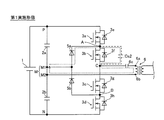
まず、図1を参照して、3レベル電力変換装置100の構成について説明する。図1に示すように、3レベル電力変換装置100は、直流電源1を備える。また、3レベル電力変換装置100は、直流電源1に並列に接続されるコンデンサ回路2を備える。コンデンサ回路2は、互いに直列に接続されたコンデンサ2aとコンデンサ2bとを含む。なお、直流電源1は、直流電圧Eを出力する。
(Configuration of 3-level power converter)
First, the configuration of the three-
また、3レベル電力変換装置100は、コンデンサ回路2に並列に接続されるスイッチング回路3を備える。スイッチング回路3において、第1半導体スイッチング素子3a、第2半導体スイッチング素子3b、第3半導体スイッチング素子3c、第4半導体スイッチング素子3dがこの順に正電圧側から負電圧側に向かって直列に接続されている。また、スイッチング回路3は、第1半導体スイッチング素子3a、第2半導体スイッチング素子3b、第3半導体スイッチング素子3c、および、第4半導体スイッチング素子3dの各々に逆並列に接続された、ダイオード3e、ダイオード3f、ダイオード3g、および、ダイオード3hを含む。なお、第1半導体スイッチング素子3a、第2半導体スイッチング素子3b、第3半導体スイッチング素子3c、および、第4半導体スイッチング素子3dの各々は、多層配線基板4(図2参照)上に実装されている。
Further, the three-level
また、3レベル電力変換装置100には、ダイオード5aとダイオード5bとが設けられている。ダイオード5aは、コンデンサ2aとコンデンサ2bとの間の直流中点M(M1)と、第1半導体スイッチング素子3aと第2半導体スイッチング素子3bとの間の接続点Aとの間に設けられている。具体的には、ダイオード5aのアノードと直流中点M(M1)とが接続されている。また、ダイオード5aのカソードと接続点Aとが接続されている。
Further, the three-
また、ダイオード5bは、直流中点M1と、第3半導体スイッチング素子3cおよび第4半導体スイッチング素子3dの間の接続点Bとの間に設けられている。具体的には、ダイオード5bのカソードと直流中点M1とが接続されている。また、ダイオード5bのアノードと接続点Bとが接続されている。また、ダイオード5aのアノードとダイオード5bのカソードとは接続されている。
Further, the
また、3レベル電力変換装置100には、絶縁トランス6が設けられている。絶縁トランス6の一方側の端子6aは、第2半導体スイッチング素子3bと第3半導体スイッチング素子3cとの間の接続点Cに接続されている。また、絶縁トランス6の他方側の端子6bは、コンデンサ2aとコンデンサ2bとの間の直流中点M(M2)に接続されている。なお、絶縁トランス6の端子6aと接続点Cとの間には、直流カット用コンデンサ6cが設けられている。
Further, the three-
また、3レベル電力変換装置100は、絶縁トランス6の2次側に設けられる整流回路101を含む。スイッチング回路3に含まれる各半導体スイッチング素子のスイッチングにより絶縁トランス6に印加される電圧Vt(高周波交流)は、絶縁トランス6により整流回路101に伝達される。そして、整流回路101により交流から直流に変換された電圧が、整流回路101に並列に接続されている負荷102に印加される。すなわち、3レベル電力変換装置100は、DC/DCコンバータとして機能する。なお、整流回路101は、ダイオード、リアクタンス、および、コンデンサからなる回路であるが、整流回路101の回路構成はこれに限られない。
Further, the three-level
なお、第1半導体スイッチング素子3aおよび第2半導体スイッチング素子3bがオンで、かつ、第3半導体スイッチング素子3cおよび第4半導体スイッチング素子3dがオフである場合には、Vt=E/2となる。また、第3半導体スイッチング素子3cおよび第4半導体スイッチング素子3dがオンで、かつ、第1半導体スイッチング素子3aおよび第2半導体スイッチング素子3bがオフである場合には、Vt=−E/2となる。また、第2半導体スイッチング素子3bおよび第3半導体スイッチング素子3cがオンで、かつ、第1半導体スイッチング素子3aおよび第4半導体スイッチング素子3dがオフである場合には、Vt=0となる。
When the first
Vt=E/2である期間、Vt=0である期間、および、Vt=−E/2である期間の比率が制御(PWM制御)されることにより、負荷102に印加される電圧が制御される。
The voltage applied to the
図2に示すように、第1半導体スイッチング素子3a、第2半導体スイッチング素子3b、第3半導体スイッチング素子3c、および、第4半導体スイッチング素子3dは、多層配線基板4の実装面4a上において、所定の方向(X方向)に並んで配置されている。なお、図2は概略図である。
As shown in FIG. 2, the first
また、多層配線基板4は、第1半導体スイッチング素子3a、第2半導体スイッチング素子3b、第3半導体スイッチング素子3c、および、第4半導体スイッチング素子3dの各々のソース端子Sに接続されている、ソース端子側基板配線10a、ソース端子側基板配線10b、ソース端子側基板配線10c、および、ソース端子側基板配線10dを含む。また、多層配線基板4は、第1半導体スイッチング素子3a、第2半導体スイッチング素子3b、第3半導体スイッチング素子3c、および、第4半導体スイッチング素子3dの各々のドレイン端子D(図2(b)参照)に接続されている、ドレイン端子側基板配線20a、ドレイン端子側基板配線20b、ドレイン端子側基板配線20c、および、ドレイン端子側基板配線20dを含む。なお、上記の各ソース端子側基板配線(10a、10b、10c、10d)および各ドレイン端子側基板配線(20a、20b、20c、20d)により、接続されている半導体スイッチング素子(3a、3b、3c、3d)の放熱(冷却)がされている。
Further, the multilayer wiring board 4 is connected to the source terminals S of the first
また、ソース端子側基板配線10aとドレイン端子側基板配線20bとの組、ソース端子側基板配線10bとドレイン端子側基板配線20cとの組、および、ソース端子側基板配線10cとドレイン端子側基板配線20dとの組の各々は、一体的に形成されている。
Further, a set of the source terminal
また、第1半導体スイッチング素子3aのソース端子側基板配線10aとドレイン端子側基板配線20aとの間には、寄生容量Cs1(図4参照)が生じる。また、第2半導体スイッチング素子3bのソース端子側基板配線10bとドレイン端子側基板配線20bとの間には、寄生容量Cs2(図6参照)が生じる。第3半導体スイッチング素子3cのソース端子側基板配線10cとドレイン端子側基板配線20cとの間には、寄生容量Cs3(図示せず)が生じる。また、第4半導体スイッチング素子3dのソース端子側基板配線10dとドレイン端子側基板配線20dとの間には、寄生容量Cs4(図示せず)が生じる。
Further, a parasitic capacitance Cs1 (see FIG. 4) is generated between the source terminal
ここで、第1実施形態では、寄生容量Cs1と寄生容量Cs4とが互いに等しいとともに、寄生容量Cs2と寄生容量Cs3とが互いに等しくなるように、多層配線基板4の実装面4aに略垂直な方向(Z1方向側)から見て、第1半導体スイッチング素子3a、第2半導体スイッチング素子3b、第3半導体スイッチング素子3c、および、第4半導体スイッチング素子3dの各々の、ソース端子側基板配線(10a、10b、10c、10d)とドレイン端子側基板配線(20a、20b、20c、20d)との重なり具合が調整されている。なお、重なり具合とは、たとえば多層配線基板4の実装面に略垂直な方向(Z1方向側)から見て、ソース端子側基板配線(10a、10b、10c、10d)とドレイン端子側基板配線(20a、20b、20c、20d)とが重なっている面積のことである。ただし、ソース端子側基板配線(10a、10b、10c、10d)とドレイン端子側基板配線(20a、20b、20c、20d)とが重なることで形成される寄生容量が等しく調整されていればこれに限らない。
Here, in the first embodiment, the direction substantially perpendicular to the mounting
具体的には、寄生容量Cs1と寄生容量Cs4とが互いに等しくなるように、多層配線基板4の実装面4aに略垂直な方向(Z1方向側)から見て、第1半導体スイッチング素子3aのソース端子側基板配線10aおよびドレイン端子側基板配線20aの重なり具合と、第4半導体スイッチング素子3dのソース端子側基板配線10dおよびドレイン端子側基板配線20dの重なり具合とが同一になるように調整されている。また、寄生容量Cs2と寄生容量Cs3とが互いに等しくなるように、多層配線基板4の実装面4aに略垂直な方向(Z1方向側)から見て、第2半導体スイッチング素子3bのソース端子側基板配線10bおよびドレイン端子側基板配線20bの重なり具合と、第3半導体スイッチング素子3cのソース端子側基板配線10cおよびドレイン端子側基板配線20cの重なり具合とが同一になるように調整されている。
Specifically, the source of the first
詳細には、多層配線基板4の実装面4aに略垂直な方向(Z1方向側)から見て、第1半導体スイッチング素子3a、第2半導体スイッチング素子3b、第3半導体スイッチング素子3c、および、第4半導体スイッチング素子3dの各々の、ソース端子側基板配線(10a、10b、10c、10d)とドレイン端子側基板配線(20a、20b、20c、20d)とは互いに重ならないように調整されている。すなわち、寄生容量Cs1、Cs2、Cs3、および、Cs4は互いに略等しい。
Specifically, the first
また、第1実施形態では、図2(b)に示すように、第1半導体スイッチング素子3aのドレイン端子側基板配線20aのうちの一部は、第1半導体スイッチング素子3aのソース端子側基板配線10aが配線されている多層配線基板4内の配線層とは異なる層の配線層を含んでいる。また、第4半導体スイッチング素子3dのソース端子側基板配線10dのうちの一部は、第4半導体スイッチング素子3dのドレイン端子側基板配線20dが配線されている多層配線基板4内の配線層とは異なる層の配線層を含んでいる。
Further, in the first embodiment, as shown in FIG. 2B, a part of the drain terminal
具体的には、第1半導体スイッチング素子3aのドレイン端子側基板配線20a、および、第4半導体スイッチング素子3dのソース端子側基板配線10dの各々は、互いに異なる4層の配線層からなる。また、第1半導体スイッチング素子3aのソース端子側基板配線10a、および、第4半導体スイッチング素子3dのドレイン端子側基板配線20dの各々は、互いに異なる2層の配線層からなる。なお、互いに異なる配線層に配線されている共通の基板配線は、ビア103により電気的に接続されている。
Specifically, each of the drain terminal
詳細には、第1半導体スイッチング素子3aのドレイン端子側基板配線20aのZ2方向側の2つの配線層は、第1半導体スイッチング素子3aのソース端子側基板配線10aが配線されている配線層とは異なる。また、第4半導体スイッチング素子3dのソース端子側基板配線10dのZ2方向側の2つの配線層は、第4半導体スイッチング素子3dのドレイン端子側基板配線20dが配線されている配線層とは異なる。
Specifically, the two wiring layers on the Z2 direction side of the drain terminal
これにより、第1半導体スイッチング素子3aのソース端子側基板配線10aとドレイン端子側基板配線20aとの間の寄生容量Cs1が増加するのを抑制しながら、ソース端子側基板配線10aが配線されている配線層とは異なる層に配線されているドレイン端子側基板配線20aを設けることによって、第1半導体スイッチング素子3aのドレイン容量(ドレイン側の容量)を増加させることが可能である。また、同様に、第4半導体スイッチング素子3dのソース端子側基板配線10dとドレイン端子側基板配線20dとの間の寄生容量Cs4が増加するのを抑制しながら、第4半導体スイッチング素子3dのソース容量(ソース側の容量)を増加させることが可能である。
As a result, the source terminal
なお、第2半導体スイッチング素子3bのソース端子側基板配線10b(第3半導体スイッチング素子3cのドレイン端子側基板配線20c)は、第1半導体スイッチング素子3aのソース端子側基板配線10a(第4半導体スイッチング素子3dのドレイン端子側基板配線20d)が配線されている2つの配線層と同じ層に配線されている。なお、各半導体スイッチング素子(3a、3b、3c、3d)のソース端子側基板配線(10a、10b、10c、10d)およびドレイン端子側基板配線(20a、20b、20c、20d)の配線層数および配線層の高さ位置などは一例であり、上記した構成に限られない。
The source terminal
(3レベル電力変換装置の動作)
まず、図3〜図8を参照して、3レベル電力変換装置100の動作について説明する。図3に示すように、第1半導体スイッチング素子3aおよび第2半導体スイッチング素子3bがオンで、かつ、第3半導体スイッチング素子3cおよび第4半導体スイッチング素子3dがオフである状態(正電圧モード)では、コンデンサ2aの放電により、電流(図3の破線の矢印)が、コンデンサ2a、第1半導体スイッチング素子3a、第2半導体スイッチング素子3b、直流カット用コンデンサ6c、絶縁トランス6のルートを流れる。なお、コンデンサ2aに流れる電流波形(図7の実線を参照)、および、コンデンサ2bに流れる電流波形(図7の破線を参照)に示すように、この正電圧モード中(図7参照)では、コンデンサ2aは放電されているとともにコンデンサ2bは充電されている。
(Operation of 3-level power converter)
First, the operation of the three-level
次に、図4に示すように、正電圧モード中に第1半導体スイッチング素子3aだけがオフされる。この場合、コンデンサ2aの放電により、電流(図4の破線の矢印)が、コンデンサ2a、寄生容量Cs1、第2半導体スイッチング素子3b、直流カット用コンデンサ6c、絶縁トランス6のルートを流れる。これにより、第1半導体スイッチング素子3aの寄生容量Cs1が、コンデンサ2aの放電により充電される。なお、第1半導体スイッチング素子3aがオフされて所定の時間後(または略同時)に第3半導体スイッチング素子3cがオンされる。
Next, as shown in FIG. 4, only the first
この場合、寄生容量Cs1の電圧がPM間の電圧(E/2)に達するまで、コンデンサ2aの放電が継続されるとともに、正電圧モードが継続される。そして、寄生容量Cs1の電圧がPM間の電圧(E/2)に達したら、還流モード(図7参照)に遷移する。すなわち、寄生容量Cs1が大きいほど、正電圧モードの時間が長くなるとともに、その分、還流モードの時間が短くなる。
In this case, the discharge of the
次に、図5に示すように、還流モード(図7参照)中において第2半導体スイッチング素子3bがオンされている間は、電流(図5の破線の矢印)は、ダイオード5a、第2半導体スイッチング素子3b、直流カット用コンデンサ6c、絶縁トランス6のルートを流れる。なお、還流モード中は、コンデンサ2aおよびコンデンサ2bの充放電は行われない。
Next, as shown in FIG. 5, while the second
次に、図6に示すように、還流モード中において、第2半導体スイッチング素子3bがオフされる。この場合、電流(図6の破線の矢印)は、ダイオード5a、寄生容量Cs2、直流カット用コンデンサ6c、絶縁トランス6のルートを流れる。この電流により、第2半導体スイッチング素子3bの寄生容量Cs2が充電される。
Next, as shown in FIG. 6, the second
この場合、寄生容量Cs2の電圧がMN間の電圧(E/2)に達するまで電流が流れ続け、還流モードが継続される。そして、寄生容量Cs2の電圧がMN間の電圧(E/2)に達したら、負電圧モード(第1半導体スイッチング素子3aおよび第2半導体スイッチング素子3bがオフで、かつ、第3半導体スイッチング素子3cおよび第4半導体スイッチング素子3dがオンである状態)に遷移する。すなわち、寄生容量Cs2が大きいほど、還流モードの時間が長くなるとともに、その分、負電圧モードの時間が短くなる。
In this case, the current continues to flow until the voltage of the parasitic capacitance Cs2 reaches the voltage between MNs (E / 2), and the reflux mode is continued. Then, when the voltage of the parasitic capacitance Cs2 reaches the voltage between MNs (E / 2), the negative voltage mode (the first
また、図8に示すように、負電圧モードから正電圧モードに遷移する場合でも、上記した動作原理と略同じであるので詳細な説明は省略するが、寄生容量Cs4が大きいほど、負電圧モードの時間が長くなるとともに、その分、還流モードの時間が短くなる。また、寄生容量Cs3が大きいほど、還流モードの時間が長くなるとともに、その分、正電圧モードの時間が短くなる。 Further, as shown in FIG. 8, even when transitioning from the negative voltage mode to the positive voltage mode, since the operating principle is substantially the same as described above, detailed description thereof will be omitted, but the larger the parasitic capacitance Cs4, the more the negative voltage mode. As the time increases, the time in the reflux mode becomes shorter accordingly. Further, the larger the parasitic capacitance Cs3, the longer the time in the reflux mode and the shorter the time in the positive voltage mode.
したがって、寄生容量Cs1の大きさと寄生容量Cs4の大きさを等しくするとともに、寄生容量Cs2の大きさと寄生容量Cs3の大きさを等しくすることによって、コンデンサ2aおよびコンデンサ2bの充放電の時間(および充電電圧)のアンバランスを解消することが可能である。その結果、正電圧モードと負電圧モードとを複数回(高速で)スイッチングする場合においても、コンデンサ2aおよびコンデンサ2bの充電電圧のばらつきが蓄積されるのを抑制することが可能である。
Therefore, by making the size of the parasitic capacitance Cs1 equal to the size of the parasitic capacitance Cs4 and making the size of the parasitic capacitance Cs2 equal to the size of the parasitic capacitance Cs3, the charging / discharging time (and charging) of the
(第1実施形態の効果)
第1実施形態では、以下のような効果を得ることができる。
(Effect of the first embodiment)
In the first embodiment, the following effects can be obtained.
第1実施形態では、上記のように、多層配線基板4の実装面4aに略垂直な方向から見て、第1半導体スイッチング素子3a、第2半導体スイッチング素子3b、第3半導体スイッチング素子3c、および、第4半導体スイッチング素子3dの各々の、ソース端子側基板配線(10a、10b、10c、10d)とドレイン端子側基板配線(20a、20b、20c、20d)との重なり具合が調整されるように、3レベル電力変換装置100を構成する。
In the first embodiment, as described above, the first
ここで、各半導体スイッチング素子の寄生容量の充電に要する時間の長さが互いに異なる場合、各半導体スイッチング素子のオンオフに要する時間にも互いに差異が生じる。このため、第1半導体スイッチング素子3aおよび第4半導体スイッチング素子3dの寄生容量(Cs1、Cs4)が互いに異なるか、または、第2半導体スイッチング素子3bおよび第3半導体スイッチング素子3cの寄生容量(Cs2、Cs3)が互いに異なる場合、コンデンサ2aを充放電する時間と、コンデンサ2bを充放電する時間との間に差異が生じる。これに対して、ソース端子側基板配線(10a、10b、10c、10d)とドレイン端子側基板配線(20a、20b、20c、20d)との重なり具合を調整することによって、第1半導体スイッチング素子3aおよび第4半導体スイッチング素子3dの寄生容量(Cs1、Cs4)を略等しくすることができるとともに、第2半導体スイッチング素子3bおよび第3半導体スイッチング素子3cの寄生容量(Cs2、Cs3)を略等しくすることができる。これにより、コンデンサ2aを充放電する時間と、コンデンサ2bを充放電する時間との間に差が生じるのを抑制することができる。その結果、コンデンサ2aに充電される電圧と、コンデンサ2bに充電される電圧との間に差が生じるのを抑制することができるとともに、コンデンサ2aおよびコンデンサ2bの充電電圧が過大になるのを抑制することができる。これにより、コンデンサ2aおよびコンデンサ2bに並列に接続されている、第1半導体スイッチング素子3a、第2半導体スイッチング素子3b、第3半導体スイッチング素子3c、および、第4半導体スイッチング素子3dの各々に過大な電圧が印加されるのを抑制することができる。
Here, when the lengths of time required to charge the parasitic capacitance of each semiconductor switching element are different from each other, the time required to turn on / off each semiconductor switching element also differs from each other. Therefore, the parasitic capacitances (Cs1, Cs4) of the first
また、ソース端子側基板配線(10a、10b、10c、10d)とドレイン端子側基板配線(20a、20b、20c、20d)との重なり具合という可視的なパラメータを調整すればよいので、比較的容易に寄生容量の調整を行うことができる。 Further, it is relatively easy because it is sufficient to adjust the visible parameter such as the degree of overlap between the source terminal side board wiring (10a, 10b, 10c, 10d) and the drain terminal side board wiring (20a, 20b, 20c, 20d). The parasitic capacitance can be adjusted.
また、第1実施形態では、上記のように、多層配線基板4の実装面4aに略垂直な方向から見て、第1半導体スイッチング素子3aのソース端子側基板配線10aおよびドレイン端子側基板配線20aの重なり具合と、第4半導体スイッチング素子3dのソース端子側基板配線10dおよびドレイン端子側基板配線20dの重なり具合とが同一である。また、多層配線基板4の実装面4aに略垂直な方向から見て、第2半導体スイッチング素子3bのソース端子側基板配線10bおよびドレイン端子側基板配線20bの重なり具合と、第3半導体スイッチング素子3cのソース端子側基板配線10cおよびドレイン端子側基板配線20cの重なり具合とが同一となるように、3レベル電力変換装置100を構成する。これにより、第1半導体スイッチング素子3a(第2半導体スイッチング素子3b)のソース端子側基板配線10a(10b)およびドレイン端子側基板配線20a(20b)の重なり具合と、第4半導体スイッチング素子3d(第3半導体スイッチング素子3c)のソース端子側基板配線10d(10c)およびドレイン端子側基板配線20d(20c)の重なり具合とを同一にすることによって、互いに異なる重なり具合を別個に設定する場合に比べて、比較的容易に寄生容量の調整を行うことができる。その結果、比較的容易に、第1半導体スイッチング素子3aおよび第4半導体スイッチング素子3dの寄生容量(Cs1、Cs4)を略等しくすることができるとともに、第2半導体スイッチング素子3bおよび第3半導体スイッチング素子3cの寄生容量(Cs2、Cs3)を略等しくすることができる。
Further, in the first embodiment, as described above, the source terminal
また、第1実施形態では、上記のように、多層配線基板4の実装面4aに略垂直な方向から見て、第1半導体スイッチング素子3a、第2半導体スイッチング素子3b、第3半導体スイッチング素子3c、および、第4半導体スイッチング素子3dの各々の、ソース端子側基板配線(10a、10b、10c、10d)とドレイン端子側基板配線(20a、20b、20c、20d)とが互いに重ならないように、3レベル電力変換装置100を構成する。これにより、ソース端子側基板配線(10a、10b、10c、10d)とレイン端子側基板配線(20a、20b、20c、20d)とを重ねるとともに重なり量(重なり部分の面積)の調整をする必要がないので、配線位置の調整作業をさらに簡易化することができる。
Further, in the first embodiment, as described above, the first
[第2実施形態]
次に、図1および図9を参照して、第2実施形態による3レベル電力変換装置300の構成について説明する。この第2実施形態における3レベル電力変換装置300では、ソース端子側基板配線とドレイン端子側基板配線とが重ならないように配線されている第1実施形態とは異なり、ソース端子側基板配線とドレイン端子側基板配線とは重なっている。なお、上記第1実施形態と同様の構成は、第1実施形態と同じ符号を付して図示するとともに説明を省略する。
[Second Embodiment]
Next, the configuration of the three-level
図9に示すように、3レベル電力変換装置300は、第1半導体スイッチング素子13aと、第2半導体スイッチング素子13bと、第3半導体スイッチング素子13cと、第4半導体スイッチング素子13dとを含むスイッチング回路13(図1参照)を備える。なお、図9は概略図である。
As shown in FIG. 9, the three-level
第1半導体スイッチング素子13a、第2半導体スイッチング素子13b、第3半導体スイッチング素子13c、および、第4半導体スイッチング素子13dの各々は、多層配線基板14上において実装されている。
Each of the first
多層配線基板14は、第1半導体スイッチング素子13a、第2半導体スイッチング素子13b、第3半導体スイッチング素子13c、および、第4半導体スイッチング素子13dの各々のソース端子Sに接続されている、ソース端子側基板配線30a、ソース端子側基板配線30b、ソース端子側基板配線30c、および、ソース端子側基板配線30dを含む。
The
また、多層配線基板14は、第1半導体スイッチング素子13a、第2半導体スイッチング素子13b、第3半導体スイッチング素子13c、および、第4半導体スイッチング素子13dの各々のドレイン端子D(図9(b)参照)に接続されている、ドレイン端子側基板配線40a、ドレイン端子側基板配線40b、ドレイン端子側基板配線40c、および、ドレイン端子側基板配線40dを含む。
Further, the
ソース端子側基板配線30aとドレイン端子側基板配線40bとの組、ソース端子側基板配線30bとドレイン端子側基板配線40cとの組、ソース端子側基板配線30cとドレイン端子側基板配線40dとの組の各々は、一体的に形成されている。
A set of the source terminal
ソース端子側基板配線30b(ドレイン端子側基板配線40c)、および、ドレイン端子側基板配線40d(ソース端子側基板配線30c)の各々は、互いに異なる3層の配線層からなる。また、ソース端子側基板配線30b(ドレイン端子側基板配線40c)、および、ドレイン端子側基板配線40d(ソース端子側基板配線30c)の各々の最下層(Z2方向側から1番目の層)は、ドレイン端子側基板配線40aおよびソース端子側基板配線30dの最下層(Z2方向側から1番目の層)と同じ層である。なお、各半導体スイッチング素子(13a、13b、13c、13d)のソース端子側基板配線(30a、30b、30c、30d)およびドレイン端子側基板配線(40a、40b、40c、40d)の配線層数および配線層の高さ位置などは一例であり、上記した構成に限られない。
Each of the source terminal
ここで、第2実施形態では、多層配線基板14の実装面14aに略垂直な方向(Z1方向側)から見て、第1半導体スイッチング素子13a、第2半導体スイッチング素子13b、第3半導体スイッチング素子13c、および、第4半導体スイッチング素子13dの各々の、ソース端子側基板配線(30a、30b、30c、30d)およびドレイン端子側基板配線(40a、40b、40c、40d)の重なり量および重なり部分の配線間距離は互いに略等しい。
Here, in the second embodiment, the first
具体的には、各半導体スイッチング素子において、ソース端子側基板配線(30a、30b、30c、30d)およびドレイン端子側基板配線(40a、40b、40c、40d)の重なり部分の、X方向の幅は幅W1(図9(b)参照)を有するとともにY方向の幅は幅W2(図9(a)参照)を有する。すなわち、各半導体スイッチング素子において、多層配線基板14の実装面14aに略垂直な方向(Z1方向側)から見た、ソース端子側基板配線(30a、30b、30c、30d)およびドレイン端子側基板配線(40a、40b、40c、40d)の重なり部分(図9(a)のハッチング部分)の面積はW1×W2である。
Specifically, in each semiconductor switching element, the width of the overlapping portion of the source terminal side board wiring (30a, 30b, 30c, 30d) and the drain terminal side board wiring (40a, 40b, 40c, 40d) in the X direction is It has a width W1 (see FIG. 9B) and a width in the Y direction has a width W2 (see FIG. 9A). That is, in each semiconductor switching element, the source terminal side board wiring (30a, 30b, 30c, 30d) and the drain terminal side board wiring as viewed from the direction substantially perpendicular to the mounting
また、各半導体スイッチング素子において、ソース端子側基板配線(30a、30b、30c、30d)およびドレイン端子側基板配線(40a、40b、40c、40d)の重なり部分の配線間距離は距離dを有する。具体的には、各半導体スイッチング素子の重なり部分において、ソース端子側基板配線(30a、30b、30c、30d)およびドレイン端子側基板配線(40a、40b、40c、40d)は、Z1方向側から2層目の配線層とZ1方向側から4番目の配線層との間の距離dだけ離間している。 Further, in each semiconductor switching element, the distance between the wirings of the overlapping portions of the source terminal side substrate wirings (30a, 30b, 30c, 30d) and the drain terminal side substrate wirings (40a, 40b, 40c, 40d) has a distance d. Specifically, in the overlapping portion of each semiconductor switching element, the source terminal side board wiring (30a, 30b, 30c, 30d) and the drain terminal side board wiring (40a, 40b, 40c, 40d) are 2 from the Z1 direction side. The wiring layer of the first layer and the fourth wiring layer from the Z1 direction side are separated by a distance d.
第2実施形態のその他の構成は、上記第1実施形態と同様である。 Other configurations of the second embodiment are the same as those of the first embodiment.
(第2実施形態の効果)
第2実施形態では、以下のような効果を得ることができる。
(Effect of the second embodiment)
In the second embodiment, the following effects can be obtained.
第2実施形態では、上記のように、多層配線基板14の実装面14aに略垂直な方向から見て、第1半導体スイッチング素子13a、第2半導体スイッチング素子13b、第3半導体スイッチング素子13c、および、第4半導体スイッチング素子13dの各々の、ソース端子側基板配線(30a、30b、30c、30d)およびドレイン端子側基板配線(40a、40b、40c、40d)の重なり量および重なり部分の配線間距離が互いに略等しくなるように、3レベル電力変換装置300を構成する。これにより、各々の半導体スイッチング素子の、ソース端子側基板配線(30a、30b、30c、30d)およびドレイン端子側基板配線(40a、40b、40c、40d)が重ならないように構成する場合に比べて、多層配線基板14の実装面14aに略垂直な方向から見て、基板配線が設けられる領域の面積を小さくすることができる。その結果、3レベル電力変換装置300の小型化を容易に図ることができる。
In the second embodiment, as described above, the first
なお、第2実施形態のその他の効果は、上記第1実施形態と同様である。 The other effects of the second embodiment are the same as those of the first embodiment.
[変形例]
なお、今回開示された実施形態は、すべての点で例示であって制限的なものではないと考えられるべきである。本発明の範囲は、上記した実施形態の説明ではなく特許請求の範囲によって示され、さらに特許請求の範囲と均等の意味および範囲内でのすべての変更(変形例)が含まれる。
[Modification example]
It should be noted that the embodiments disclosed this time are exemplary in all respects and are not considered to be restrictive. The scope of the present invention is shown by the scope of claims rather than the description of the above-described embodiment, and further includes all modifications (modifications) within the meaning and scope equivalent to the scope of claims.
たとえば、上記第1実施形態では、第1半導体スイッチング素子、第2半導体スイッチング素子、第3半導体スイッチング素子、および、第4半導体スイッチング素子の各々の、ソース端子側基板配線とドレイン端子側基板配線とが重なっていない例を示したが、本発明はこれに限られない。たとえば、多層配線基板の実装面に略垂直な方向から見て、第1半導体スイッチング素子および第4半導体スイッチング素子の組と、第2半導体スイッチング素子および第3半導体スイッチング素子の組とのうちのいずれか一方の組が、各々のソース端子側基板配線とドレイン端子側基板配線とが互いに重ならないように構成されていてもよい。 For example, in the first embodiment, the source terminal side board wiring and the drain terminal side board wiring of each of the first semiconductor switching element, the second semiconductor switching element, the third semiconductor switching element, and the fourth semiconductor switching element. Although an example in which they do not overlap is shown, the present invention is not limited to this. For example, any of a set of the first semiconductor switching element and the fourth semiconductor switching element and a set of the second semiconductor switching element and the third semiconductor switching element when viewed from a direction substantially perpendicular to the mounting surface of the multilayer wiring board. One set may be configured so that the source terminal side board wiring and the drain terminal side board wiring do not overlap each other.
たとえば、図10に示すように、3レベル電力変換装置500には、第1半導体スイッチング素子23a、第2半導体スイッチング素子23b、第3半導体スイッチング素子23c、および、第4半導体スイッチング素子23dが設けられている。
For example, as shown in FIG. 10, the three-
多層配線基板14は、第1半導体スイッチング素子23a、第2半導体スイッチング素子23b、第3半導体スイッチング素子23c、および、第4半導体スイッチング素子23dの各々のソース端子Sに接続されている、ソース端子側基板配線50a、ソース端子側基板配線50b、ソース端子側基板配線50c、および、ソース端子側基板配線50dを含む。また、多層配線基板24は、第1半導体スイッチング素子23a、第2半導体スイッチング素子23b、第3半導体スイッチング素子23c、および、第4半導体スイッチング素子23dの各々のドレイン端子D(図2(b)参照)に接続されている、ドレイン端子側基板配線60a、ドレイン端子側基板配線60b、ドレイン端子側基板配線60c、および、ドレイン端子側基板配線60dを含む。
The
多層配線基板24の実装面24aに略垂直な方向(Z1方向側)から見て、ドレイン端子側基板配線60aと、ソース端子側基板配線50aとは重なっていない。また、多層配線基板24の実装面24aに略垂直な方向(Z1方向側)から見て、ドレイン端子側基板配線60dと、ソース端子側基板配線50dとは重なっていない。
The drain terminal
また、ドレイン端子側基板配線60bとソース端子側基板配線50bとの重なり部分(図10(a)のハッチング部分参照)の重なり量(W1×W2)および重なり部分の配線間距離(d)は、ドレイン端子側基板配線60cとソース端子側基板配線50cとの重なり部分(図10(a)のハッチング部分参照)の重なり量(W1×W2)および重なり部分の配線間距離(d)と等しい。
Further, the overlapping amount (W1 × W2) of the overlapping portion (see the hatched portion in FIG. 10A) between the drain terminal
なお、第1半導体スイッチング素子および第4半導体スイッチング素子の、各々のソース端子側基板配線とドレイン端子側基板配線との重なり量および重なり部分の配線間距離が互いに等しく、第2半導体スイッチング素子および第3半導体スイッチング素子の、各々のソース端子側基板配線とドレイン端子側基板配線とが互いに重ならないように構成されていてもよい。 The amount of overlap between the source terminal side board wiring and the drain terminal side board wiring of the first semiconductor switching element and the fourth semiconductor switching element and the distance between the wirings of the overlapping portions are equal to each other, and the second semiconductor switching element and the second semiconductor switching element and the first 3 The semiconductor switching element may be configured so that the source terminal side board wiring and the drain terminal side board wiring do not overlap each other.
これにより、第1半導体スイッチング素子23aおよび第4半導体スイッチング素子23dの組と、第2半導体スイッチング素子23bおよび第3半導体スイッチング素子23cの組との両方において、各々のソース端子側基板配線とドレイン端子側基板配線とを重ねるとともに重なり量(重なり部分の面積)を調整する場合に比べて、ソース端子側基板配線(50a、50b、50c、50d)およびドレイン端子側基板配線(60a、60b、60c、60d)の配線位置の調整作業を簡易化することができる。
As a result, in both the set of the first
また、上記第2実施形態では、ソース端子側基板配線とドレイン端子側基板配線との重なり部分の、X方向の幅(W1)およびY方向の幅(W2)の各々が、半導体スイッチング素子ごとに等しい例を示したが、本発明はこれに限られない。たとえば、重なり部分の面積が半導体スイッチング素子ごとに等しければ、X方向およびY方向の各々の幅が半導体スイッチング素子ごとに互いに異なっていてもよい。 Further, in the second embodiment, the width (W1) in the X direction and the width (W2) in the Y direction of the overlapping portion between the board wiring on the source terminal side and the board wiring on the drain terminal side are set for each semiconductor switching element. Equal examples have been shown, but the present invention is not limited to this. For example, if the areas of the overlapping portions are equal for each semiconductor switching element, the widths in the X direction and the Y direction may be different for each semiconductor switching element.
また、上記第2実施形態では、ソース端子側基板配線とドレイン端子側基板配線との重なり量および重なり部分の配線間距離が等しい例を示したが、本発明はこれに限られない。たとえば、ソース端子側基板配線とドレイン端子側基板配線との間の寄生容量が半導体スイッチング素子ごとに等しければ、ソース端子側基板配線とドレイン端子側基板配線との重なり量および重なり部分の配線間距離が、半導体スイッチング素子ごとに互いに異なっていてもよい。 Further, in the second embodiment, an example is shown in which the amount of overlap between the source terminal side board wiring and the drain terminal side board wiring and the distance between the wirings of the overlapping portions are the same, but the present invention is not limited to this. For example, if the parasitic capacitance between the source terminal side board wiring and the drain terminal side board wiring is equal for each semiconductor switching element, the amount of overlap between the source terminal side board wiring and the drain terminal side board wiring and the distance between the overlapping portions are equal. However, they may be different from each other for each semiconductor switching element.
また、上記第1および第2実施形態では、4つの半導体スイッチング素子が一列に配列されている構成の例を示したが、本発明はこれに限られない。たとえば、4つの半導体スイッチング素子が、マトリクス状に配置されていてもよい。 Further, in the first and second embodiments, an example of a configuration in which four semiconductor switching elements are arranged in a row is shown, but the present invention is not limited to this. For example, four semiconductor switching elements may be arranged in a matrix.
1 直流電源
2 コンデンサ回路
2a、2b コンデンサ
3、13 スイッチング回路
3a、13a、23a 第1半導体スイッチング素子
3b、13b、23b 第2半導体スイッチング素子
3c、13c、23c 第3半導体スイッチング素子
3d、13d、23d 第4半導体スイッチング素子
4、14、24 多層配線基板
4a、14a、24a 実装面
10a、10b、10c、10d、30a、30b、30c、30d、50a、50b、50c、50d ソース端子側基板配線
20a、20b、20c、20d、40a、40b、40c、40d、60a、60b、60c、60d ドレイン端子側基板配線
100、300、500 3レベル電力変換装置
D ドレイン端子
S ソース端子
1
Claims (5)
前記直流電源に並列に接続され、互いに直列に接続された複数のコンデンサを含むコンデンサ回路と、
前記コンデンサ回路に並列に接続されるとともに、多層配線基板上において実装され、第1半導体スイッチング素子、第2半導体スイッチング素子、第3半導体スイッチング素子、第4半導体スイッチング素子の順に正電圧側から直列に接続されているスイッチング回路と、を備え、
前記多層配線基板は、前記第1半導体スイッチング素子、前記第2半導体スイッチング素子、前記第3半導体スイッチング素子、および、前記第4半導体スイッチング素子の各々の、ソース端子に接続されているソース端子側基板配線と、ドレイン端子に接続されているドレイン端子側基板配線とを含み、
前記多層配線基板の実装面に略垂直な方向から見て、前記第1半導体スイッチング素子、前記第2半導体スイッチング素子、前記第3半導体スイッチング素子、および、前記第4半導体スイッチング素子の各々の、前記ソース端子側基板配線と前記ドレイン端子側基板配線との重なり具合が調整されている、3レベル電力変換装置。 DC power supply and
A capacitor circuit including a plurality of capacitors connected in parallel to the DC power supply and connected in series with each other.
It is connected in parallel to the capacitor circuit and mounted on a multilayer wiring board, and is connected in series from the positive voltage side in the order of the first semiconductor switching element, the second semiconductor switching element, the third semiconductor switching element, and the fourth semiconductor switching element. With a connected switching circuit,
The multilayer wiring board is a source terminal side substrate connected to a source terminal of each of the first semiconductor switching element, the second semiconductor switching element, the third semiconductor switching element, and the fourth semiconductor switching element. Including the wiring and the drain terminal side board wiring connected to the drain terminal,
Each of the first semiconductor switching element, the second semiconductor switching element, the third semiconductor switching element, and the fourth semiconductor switching element when viewed from a direction substantially perpendicular to the mounting surface of the multilayer wiring board. A three-level power conversion device in which the degree of overlap between the source terminal side board wiring and the drain terminal side board wiring is adjusted.
Priority Applications (1)
| Application Number | Priority Date | Filing Date | Title |
|---|---|---|---|
| JP2017224683A JP6950488B2 (en) | 2017-11-22 | 2017-11-22 | 3-level power converter |
Applications Claiming Priority (1)
| Application Number | Priority Date | Filing Date | Title |
|---|---|---|---|
| JP2017224683A JP6950488B2 (en) | 2017-11-22 | 2017-11-22 | 3-level power converter |
Publications (2)
| Publication Number | Publication Date |
|---|---|
| JP2019097300A JP2019097300A (en) | 2019-06-20 |
| JP6950488B2 true JP6950488B2 (en) | 2021-10-13 |
Family
ID=66973193
Family Applications (1)
| Application Number | Title | Priority Date | Filing Date |
|---|---|---|---|
| JP2017224683A Expired - Fee Related JP6950488B2 (en) | 2017-11-22 | 2017-11-22 | 3-level power converter |
Country Status (1)
| Country | Link |
|---|---|
| JP (1) | JP6950488B2 (en) |
Families Citing this family (3)
| Publication number | Priority date | Publication date | Assignee | Title |
|---|---|---|---|---|
| DE202018104586U1 (en) * | 2018-08-09 | 2019-11-19 | Sma Solar Technology Ag | DC link arrangement and inverter |
| CN121488397A (en) * | 2023-07-28 | 2026-02-06 | 松下知识产权经营株式会社 | Isolated AC/DC converter |
| CN121488398A (en) * | 2023-07-28 | 2026-02-06 | 松下知识产权经营株式会社 | Isolated AC/DC converter |
Family Cites Families (4)
| Publication number | Priority date | Publication date | Assignee | Title |
|---|---|---|---|---|
| JP5580365B2 (en) * | 2012-05-29 | 2014-08-27 | 旭化成エレクトロニクス株式会社 | Current control circuit and PLL circuit using the same |
| JP6008185B2 (en) * | 2012-11-19 | 2016-10-19 | 富士電機株式会社 | Three-level power converter and control method thereof |
| WO2016069981A1 (en) * | 2014-10-31 | 2016-05-06 | Skyworks Solutions, Inc. | Signal paths for radio-frequency modules |
| JP2017020631A (en) * | 2015-07-15 | 2017-01-26 | アズビル株式会社 | Positioner |
-
2017
- 2017-11-22 JP JP2017224683A patent/JP6950488B2/en not_active Expired - Fee Related
Also Published As
| Publication number | Publication date |
|---|---|
| JP2019097300A (en) | 2019-06-20 |
Similar Documents
| Publication | Publication Date | Title |
|---|---|---|
| JP5798412B2 (en) | Semiconductor module | |
| JP5867472B2 (en) | Power converter | |
| JP6950488B2 (en) | 3-level power converter | |
| CN101807863B (en) | Power converter | |
| JP6549200B2 (en) | Power conversion circuit | |
| JP5347565B2 (en) | Power conversion unit | |
| JPWO2015053142A1 (en) | Driver board and power conversion device | |
| JP2013027232A (en) | Power converter | |
| JP2015106601A (en) | Semiconductor device | |
| JP6946971B2 (en) | Power converter | |
| JP2008263755A (en) | Switching power supply | |
| JP7043887B2 (en) | 3-level power converter | |
| JP2012110231A (en) | Power conversion device | |
| JP6365172B2 (en) | Power conversion device and device parts | |
| JP6398287B2 (en) | Planar type transformer and switching power supply circuit | |
| WO2021019603A1 (en) | Power conversion device | |
| JP2019004633A (en) | Power converter | |
| JP2013258863A (en) | Multilevel power converter | |
| US10725487B2 (en) | Power circuit including ballast element | |
| JP2013004683A (en) | Power converter of printed board | |
| JP7317074B2 (en) | power converter | |
| JP2018182850A (en) | Power converter | |
| JP6429246B2 (en) | Power circuit | |
| US12308743B2 (en) | Single inductor converter with current loops in opposite directions | |
| JPWO2021074981A1 (en) | DC / DC converter device |
Legal Events
| Date | Code | Title | Description |
|---|---|---|---|
| A621 | Written request for application examination |
Free format text: JAPANESE INTERMEDIATE CODE: A621 Effective date: 20201014 |
|
| A977 | Report on retrieval |
Free format text: JAPANESE INTERMEDIATE CODE: A971007 Effective date: 20210817 |
|
| TRDD | Decision of grant or rejection written | ||
| A01 | Written decision to grant a patent or to grant a registration (utility model) |
Free format text: JAPANESE INTERMEDIATE CODE: A01 Effective date: 20210824 |
|
| A61 | First payment of annual fees (during grant procedure) |
Free format text: JAPANESE INTERMEDIATE CODE: A61 Effective date: 20210906 |
|
| R150 | Certificate of patent or registration of utility model |
Ref document number: 6950488 Country of ref document: JP Free format text: JAPANESE INTERMEDIATE CODE: R150 |
|
| LAPS | Cancellation because of no payment of annual fees |