JP6939542B2 - Electrical connection device - Google Patents
Electrical connection device Download PDFInfo
- Publication number
- JP6939542B2 JP6939542B2 JP2017254840A JP2017254840A JP6939542B2 JP 6939542 B2 JP6939542 B2 JP 6939542B2 JP 2017254840 A JP2017254840 A JP 2017254840A JP 2017254840 A JP2017254840 A JP 2017254840A JP 6939542 B2 JP6939542 B2 JP 6939542B2
- Authority
- JP
- Japan
- Prior art keywords
- bus bar
- terminal
- conductive plate
- insulator
- switching element
- Prior art date
- Legal status (The legal status is an assumption and is not a legal conclusion. Google has not performed a legal analysis and makes no representation as to the accuracy of the status listed.)
- Active
Links
Images


Classifications
-
- H—ELECTRICITY
- H05—ELECTRIC TECHNIQUES NOT OTHERWISE PROVIDED FOR
- H05K—PRINTED CIRCUITS; CASINGS OR CONSTRUCTIONAL DETAILS OF ELECTRIC APPARATUS; MANUFACTURE OF ASSEMBLAGES OF ELECTRICAL COMPONENTS
- H05K1/00—Printed circuits
- H05K1/18—Printed circuits structurally associated with non-printed electric components
- H05K1/182—Printed circuits structurally associated with non-printed electric components associated with components mounted in the printed circuit board, e.g. insert mounted components [IMC]
- H05K1/185—Components encapsulated in the insulating substrate of the printed circuit or incorporated in internal layers of a multilayer circuit
- H05K1/186—Components encapsulated in the insulating substrate of the printed circuit or incorporated in internal layers of a multilayer circuit manufactured by mounting on or connecting to patterned circuits before or during embedding
-
- B—PERFORMING OPERATIONS; TRANSPORTING
- B60—VEHICLES IN GENERAL
- B60R—VEHICLES, VEHICLE FITTINGS, OR VEHICLE PARTS, NOT OTHERWISE PROVIDED FOR
- B60R16/00—Electric or fluid circuits specially adapted for vehicles and not otherwise provided for; Arrangement of elements of electric or fluid circuits specially adapted for vehicles and not otherwise provided for
- B60R16/02—Electric or fluid circuits specially adapted for vehicles and not otherwise provided for; Arrangement of elements of electric or fluid circuits specially adapted for vehicles and not otherwise provided for electric constitutive elements
- B60R16/023—Electric or fluid circuits specially adapted for vehicles and not otherwise provided for; Arrangement of elements of electric or fluid circuits specially adapted for vehicles and not otherwise provided for electric constitutive elements for transmission of signals between vehicle parts or subsystems
- B60R16/0238—Electrical distribution centers
-
- H—ELECTRICITY
- H02—GENERATION; CONVERSION OR DISTRIBUTION OF ELECTRIC POWER
- H02G—INSTALLATION OF ELECTRIC CABLES OR LINES, OR OF COMBINED OPTICAL AND ELECTRIC CABLES OR LINES
- H02G3/00—Installations of electric cables or lines or protective tubing therefor in or on buildings, equivalent structures or vehicles
- H02G3/02—Details
- H02G3/08—Distribution boxes; Connection or junction boxes
- H02G3/16—Distribution boxes; Connection or junction boxes structurally associated with support for line-connecting terminals within the box
-
- H—ELECTRICITY
- H05—ELECTRIC TECHNIQUES NOT OTHERWISE PROVIDED FOR
- H05K—PRINTED CIRCUITS; CASINGS OR CONSTRUCTIONAL DETAILS OF ELECTRIC APPARATUS; MANUFACTURE OF ASSEMBLAGES OF ELECTRICAL COMPONENTS
- H05K1/00—Printed circuits
- H05K1/02—Details
- H05K1/03—Use of materials for the substrate
- H05K1/0313—Organic insulating material
-
- H—ELECTRICITY
- H05—ELECTRIC TECHNIQUES NOT OTHERWISE PROVIDED FOR
- H05K—PRINTED CIRCUITS; CASINGS OR CONSTRUCTIONAL DETAILS OF ELECTRIC APPARATUS; MANUFACTURE OF ASSEMBLAGES OF ELECTRICAL COMPONENTS
- H05K3/00—Apparatus or processes for manufacturing printed circuits
- H05K3/30—Assembling printed circuits with electric components, e.g. with resistor
- H05K3/303—Surface mounted components, e.g. affixing before soldering, aligning means, spacing means
-
- H—ELECTRICITY
- H05—ELECTRIC TECHNIQUES NOT OTHERWISE PROVIDED FOR
- H05K—PRINTED CIRCUITS; CASINGS OR CONSTRUCTIONAL DETAILS OF ELECTRIC APPARATUS; MANUFACTURE OF ASSEMBLAGES OF ELECTRICAL COMPONENTS
- H05K7/00—Constructional details common to different types of electric apparatus
- H05K7/02—Arrangements of circuit components or wiring on supporting structure
- H05K7/06—Arrangements of circuit components or wiring on supporting structure on insulating boards, e.g. wiring harnesses
-
- H—ELECTRICITY
- H05—ELECTRIC TECHNIQUES NOT OTHERWISE PROVIDED FOR
- H05K—PRINTED CIRCUITS; CASINGS OR CONSTRUCTIONAL DETAILS OF ELECTRIC APPARATUS; MANUFACTURE OF ASSEMBLAGES OF ELECTRICAL COMPONENTS
- H05K7/00—Constructional details common to different types of electric apparatus
- H05K7/14—Mounting supporting structure in casing or on frame or rack
- H05K7/1422—Printed circuit boards receptacles, e.g. stacked structures, electronic circuit modules or box like frames
- H05K7/1427—Housings
- H05K7/1432—Housings specially adapted for power drive units or power converters
- H05K7/14322—Housings specially adapted for power drive units or power converters wherein the control and power circuits of a power converter are arranged within the same casing
-
- H—ELECTRICITY
- H05—ELECTRIC TECHNIQUES NOT OTHERWISE PROVIDED FOR
- H05K—PRINTED CIRCUITS; CASINGS OR CONSTRUCTIONAL DETAILS OF ELECTRIC APPARATUS; MANUFACTURE OF ASSEMBLAGES OF ELECTRICAL COMPONENTS
- H05K2201/00—Indexing scheme relating to printed circuits covered by H05K1/00
- H05K2201/10—Details of components or other objects attached to or integrated in a printed circuit board
- H05K2201/10007—Types of components
- H05K2201/10166—Transistor
Description
本発明は電気接続装置に関する。 The present invention relates to an electrical connection device.
車両には、電源と、ヘッドランプ又はワイパー等の負荷とに接続される電気接続箱が搭載されている。電気接続箱は、電源及び負荷の電気的な接続と、この接続の遮断とを行なう(特許文献1参照)。 The vehicle is equipped with an electrical junction box that connects to a power source and a load such as a headlamp or wiper. The electrical junction box electrically connects the power supply and the load and disconnects the connection (see Patent Document 1).
特許文献1に記載の電気接続箱では、2つのバスバー(導電板)にFET(スイッチング素子)のソース端子及びドレイン端子が接続されている。FETのソース端子は、2つのバスバーの一方を介して電源(又は負荷)に接続され、FETのドレイン端子は、2つのバスバーの他方を介して負荷(又は電源)に接続されている。
In the electric junction box described in
2つのバスバーには、制御素子が実装された回路基板が載置されている。制御素子が制御信号を出力することによって、FETのオンオフが切り替えられる。FETがオンに切り替えられた場合、2つのバスバーが互いに電気的に接続されてFETに電流が流れ、電源から負荷に電力が供給される。FETがオフに切り替えられた場合、2つのバスバーが互いに電気的に遮断されてFETに流れる電流が遮断され、電源から負荷への電力供給が停止する。 A circuit board on which a control element is mounted is mounted on the two bus bars. When the control element outputs a control signal, the FET is switched on and off. When the FET is switched on, the two busbars are electrically connected to each other, a current flows through the FET, and power is supplied from the power supply to the load. When the FET is switched off, the two busbars are electrically cut off from each other, the current flowing through the FET is cut off, and the power supply from the power supply to the load is stopped.
特許文献2に記載の電子部品は、電子部品の本体と、本体に設けられている3つの端子とを備えている。3つの端子は、3つのバスバーに接続されている。本体は複数の外面を有し、3つの端子の内、第1の端子及び第2の端子夫々は、相異なる外面に設けられている。3つの端子の内、第3の端子は、第1の端子が設けられている外面に、第1の端子に隣り合うようにして設けられている。特許文献2に記載の電子部品がFETである場合、第1〜第3の端子はソース端子、ドレイン端子、及びゲート端子である。ゲート端子は、バスバーを介して回路基板の制御素子に接続されている。
The electronic component described in
近年、FETが小型化されている。小型のFETを採用することにより、電気接続箱の小型化を図ることができる。
FETの小型化に伴い、ソース端子とゲート端子との離隔距離が短縮されている。ところが、ソース端子とゲート端子との離隔距離が短いと、ソース端子に接続されるバスバーとゲート端子に接続されるバスバーとを互いに接触しないように配置することが難しい場合がある。この場合、小型のFETを用いることができず、電気接続箱の小型化を図ることができない。
In recent years, FETs have been miniaturized. By adopting a small FET, the electric junction box can be miniaturized.
With the miniaturization of FETs, the separation distance between the source terminal and the gate terminal has been shortened. However, if the separation distance between the source terminal and the gate terminal is short, it may be difficult to arrange the bus bar connected to the source terminal and the bus bar connected to the gate terminal so as not to contact each other. In this case, a small FET cannot be used, and the electric junction box cannot be miniaturized.
そこで、小型化を図ることができる電気接続装置を提供することを目的とする。 Therefore, it is an object of the present invention to provide an electric connection device capable of miniaturization.
本実施の形態に係る電気接続装置は、周縁部に切り欠きが設けられている第1導電板と、該第1導電板に非接触に隣り合う第2導電板と、前記第1導電板に接続されている第1端子、前記第2導電板に接続されている第2端子、及び制御端子を有し、該制御端子の電圧に応じてオン又はオフに切り替わるスイッチング素子とを備える電気接続装置であって、前記切り欠きに埋め込まれている絶縁体と、該絶縁体の表面に前記第1導電板に非接触に設けられており、前記制御端子が接続されている導電路とを備え、前記第1導電板及び前記第2導電板は、絶縁性を有する合成樹脂によって一体化されており、前記第1導電板及び前記第2導電板の間にある前記合成樹脂と前記スイッチング素子とは前記合成樹脂に設けられた凹部を隔てて対向している。 The electrical connection device according to the present embodiment has a first conductive plate having a notch on the peripheral edge, a second conductive plate that is non-contact adjacent to the first conductive plate, and the first conductive plate. An electrical connection device having a first terminal connected, a second terminal connected to the second conductive plate, and a switching element having a control terminal and switching on or off according to the voltage of the control terminal. It is provided with an insulator embedded in the notch and a conductive path provided on the surface of the insulator in a non-contact manner with the first conductive plate and to which the control terminal is connected . The first conductive plate and the second conductive plate are integrated with a synthetic resin having an insulating property, and the synthetic resin and the switching element between the first conductive plate and the second conductive plate are synthesized. at a recess provided in the resin that has to face.
上記によれば、小型化を図ることができる電気接続装置を提供することが可能となる。 According to the above, it is possible to provide an electric connection device that can be miniaturized.
[本実施の形態の説明]
最初に本実施の形態を列記して説明する。また、以下に記載する実施の形態の少なくとも一部を任意に組み合わせてもよい。
[Explanation of the present embodiment]
First, the present embodiments will be listed and described. In addition, at least a part of the embodiments described below may be arbitrarily combined.
(1)本実施の形態に係る電気接続装置は、周縁部に切り欠きが設けられている第1導電板と、該第1導電板に非接触に隣り合う第2導電板と、前記第1導電板に接続されている第1端子、前記第2導電板に接続されている第2端子、及び制御端子を有し、該制御端子の電圧に応じてオン又はオフに切り替わるスイッチング素子とを備える電気接続装置であって、前記切り欠きに埋め込まれている絶縁体と、該絶縁体の表面に前記第1導電板に非接触に設けられており、前記制御端子が接続されている導電路とを備える。 (1) The electrical connection device according to the present embodiment includes a first conductive plate having a notch on the peripheral edge, a second conductive plate adjacent to the first conductive plate in a non-contact manner, and the first conductive plate. It includes a first terminal connected to the conductive plate, a second terminal connected to the second conductive plate, and a switching element having a control terminal and switching on or off according to the voltage of the control terminal. An electrical connection device, an insulator embedded in the notch, and a conductive path provided on the surface of the insulator in a non-contact manner with the first conductive plate and to which the control terminal is connected. To be equipped.
本実施の形態にあっては、第1導電板の周縁部に切り欠きが設けられており、第1導電板の切り欠きに絶縁体が埋め込まれている。絶縁体の表面には導電路が設けられている。
スイッチング素子の第1端子は第1導電板に接続されている。スイッチング素子の第2端子は第2導電板に接続されている。スイッチング素子の制御端子は導電路に接続されている。
In the present embodiment, a notch is provided at the peripheral edge of the first conductive plate, and an insulator is embedded in the notch of the first conductive plate. A conductive path is provided on the surface of the insulator.
The first terminal of the switching element is connected to the first conductive plate. The second terminal of the switching element is connected to the second conductive plate. The control terminal of the switching element is connected to the conductive path.
第1導電板と絶縁体の表面に設けられる導電路との接触を防止することは容易である。故に、スイッチング素子の第1端子と制御端子との離隔距離が短くても、第1導電板と導電路とを絶縁することができる。
従って、電気接続装置を構成するスイッチング素子として、端子同士が接近配置された小型のスイッチング素子を用いることができる。この結果、電気接続装置の小型化を図ることができることができる。
It is easy to prevent the first conductive plate from coming into contact with the conductive path provided on the surface of the insulator. Therefore, even if the separation distance between the first terminal of the switching element and the control terminal is short, the first conductive plate and the conductive path can be insulated.
Therefore, as the switching element constituting the electrical connection device, a small switching element in which the terminals are closely arranged can be used. As a result, the electric connection device can be miniaturized.
(2)本実施の形態に係る電気接続装置は、前記絶縁体には金属粒子が含まれている構成が好ましい。 (2) The electrical connection device according to the present embodiment preferably has a configuration in which the insulator contains metal particles.
本実施の形態にあっては、金属粒子を含む絶縁体が第1導電板の切り欠きに埋め込まれている。
例えば、金属粒子を含む絶縁体へのレーザー光の照射によって、金属粒子を導体化し、めっきを行なうことで絶縁体の表面に導電路を設けることができる。また、一般的な絶縁体の表面に、金属ナノ粒子ペーストを印刷、焼結して導電路を設けることができる。
In the present embodiment, an insulator containing metal particles is embedded in the notch of the first conductive plate.
For example, by irradiating an insulator containing metal particles with laser light, the metal particles are made into conductors and plated, so that a conductive path can be provided on the surface of the insulator. Further, a conductive path can be provided by printing and sintering a metal nanoparticle paste on the surface of a general insulator.
(3)本実施の形態に係る電気接続装置は、前記第1導電板及び前記第2導電板は、絶縁性を有する合成樹脂によって一体化されており、前記第1導電板及び前記第2導電板の間にある前記合成樹脂と前記スイッチング素子とは間隔を隔てて対向している構成が好ましい。 (3) In the electrical connection device according to the present embodiment, the first conductive plate and the second conductive plate are integrated with a synthetic resin having an insulating property, and the first conductive plate and the second conductive plate are integrated. It is preferable that the synthetic resin between the plates and the switching element face each other at a distance from each other.
本実施の形態にあっては、第1導電板及び第2導電板の間において、第1導電板及び第2導電板を一体化している合成樹脂とスイッチング素子との間に空隙が形成される。故に、例えばスイッチング素子が発熱した場合に、合成樹脂がこの空隙に向けて熱膨張することができる。即ち、この空隙は合成樹脂の逃げしろとして機能する。 In the present embodiment, a gap is formed between the first conductive plate and the second conductive plate between the synthetic resin in which the first conductive plate and the second conductive plate are integrated and the switching element. Therefore, for example, when the switching element generates heat, the synthetic resin can thermally expand toward the voids. That is, this void functions as an escape margin for the synthetic resin.
(4)本実施の形態に係る電気接続装置は、前記第1導電板に非接触に隣り合う第3導電板と、前記第1導電板に接続されている第3端子、前記第3導電板に接続されている第4端子、及び前記導電路に接続されている第2の制御端子を有し、該第2の制御端子の電圧に応じてオン又はオフに切り替わる第2のスイッチング素子とを更に備える構成が好ましい。 (4) The electrical connection device according to the present embodiment includes a third conductive plate that is non-contact adjacent to the first conductive plate, a third terminal connected to the first conductive plate, and the third conductive plate. A fourth terminal connected to the above, and a second switching element having a second control terminal connected to the conductive path and switching on or off according to the voltage of the second control terminal. Further, a configuration provided is preferable.
本実施の形態にあっては、第2のスイッチング素子の第3端子は第1導電板に接続されている。第2のスイッチング素子の第4端子は第2導電板に接続されている。第2のスイッチング素子の第2の制御端子は導電路に接続されている。 In the present embodiment, the third terminal of the second switching element is connected to the first conductive plate. The fourth terminal of the second switching element is connected to the second conductive plate. The second control terminal of the second switching element is connected to the conductive path.
第1導電板と絶縁体の表面に設けられる導電路との接触を防止することは容易である。故に、第2のスイッチング素子の第3端子と第2の制御端子との離隔距離が短くても、第1導電板と導電路とを絶縁することができる。
従って、電気接続装置を構成するスイッチング素子として、端子同士が接近配置された小型のスイッチング素子を用いることができる。この結果、電気接続装置の小型化を図ることができることができる。
It is easy to prevent the first conductive plate from coming into contact with the conductive path provided on the surface of the insulator. Therefore, even if the separation distance between the third terminal and the second control terminal of the second switching element is short, the first conductive plate and the conductive path can be insulated.
Therefore, as the switching element constituting the electrical connection device, a small switching element in which the terminals are closely arranged can be used. As a result, the electric connection device can be miniaturized.
[本実施の形態の詳細]
本実施の形態に係る電気接続装置の具体例を、以下に図面を参照しつつ説明する。なお、本発明はこれらの例示に限定されるものではなく、特許請求の範囲によって示され、特許請求の範囲と均等の意味および範囲内でのすべての変更が含まれることが意図される。
[Details of the present embodiment]
A specific example of the electrical connection device according to the present embodiment will be described below with reference to the drawings. It should be noted that the present invention is not limited to these examples, and is indicated by the scope of claims, and is intended to include all modifications within the meaning and scope equivalent to the scope of claims.
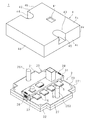
図1は、実施の形態に係る電気接続装置を備える電気接続箱の斜視図である。
図2は、電気接続箱の断面図である。
図3は、電気接続箱の分解斜視図である。
図中1は電気接続箱であり、電気接続箱1は、電気接続装置2、回路基板31、放熱部材32、及びカバー4を備えている。電気接続装置2は、第1バスバー21(第2導電板)、第2バスバー22(第1導電板)、第3バスバー23(第3導電板)、絶縁体24、8つの導電路25(図4参照)、及び2つのボルト261,262を備えている。
FIG. 1 is a perspective view of an electrical connection box including the electrical connection device according to the embodiment.
FIG. 2 is a cross-sectional view of the electrical junction box.
FIG. 3 is an exploded perspective view of the electrical junction box.
In the figure,
図4は、第1バスバー21、第2バスバー22、第3バスバー23、絶縁体24、導電路25、及びボルト261,262夫々の斜視図である。
図2〜図4に示すように、第1バスバー21は矩形板状をなす。第1バスバー21の一方の長辺部には貫通孔211が設けられている。貫通孔211は、第1バスバー21の長手方向の中央に配されている。第1バスバー21は導電性を有し、例えば金属製である。
FIG. 4 is a perspective view of the
As shown in FIGS. 2 to 4, the
第1バスバー21の貫通孔211には、ボルト261の軸部がかしめられている。ボルト261の軸部は、第1バスバー21の一面に直交する方向に、第1バスバー21の一面から突出している。ボルト261の頭部は、第1バスバー21の他面に接触している。
第3バスバー23の構成は第1バスバー21の構成と同様である。ボルト262の軸部は、第3バスバー23の貫通孔231にかしめられている。
The shaft portion of the
The configuration of the
図5は、第2バスバー22単体の斜視図である。
図2、図4、及び図5に示すように、第2バスバー22は矩形板状をなす。第2バスバー22の各長辺部には、3つの切り欠き221が並設されている。第2バスバー22の一方の長辺部の3つの切り欠き221と第2バスバー22の他方の長辺部の3つの切り欠き221とは千鳥状に配されている。各切り欠き221は矩形状をなす。図5に示す第2バスバー22の下向きの面及び上向きの面を、以下では第2バスバー22の下面22a及び上面22bという。
第1バスバー21、第2バスバー22、及び第3バスバー23夫々の厚みは互いに同程度である。
第2バスバー22には、絶縁体24が一体に設けられている。
FIG. 5 is a perspective view of the
As shown in FIGS. 2, 4, and 5, the
The thicknesses of the
An
図6は、第2バスバー22に絶縁体24が設けられた状態の斜視図である。
絶縁体24は、絶縁性を有する合成樹脂に多数の金属粒子が分散しているものである。絶縁体24は、絶縁層241、6つの端子受け242、2つの端子受け243、及び2つの突出片244を一体に有する。
絶縁層241は第2バスバー22の下面22aに積層されており、第2バスバー22の6つの切り欠き221を覆っている。
端子受け242は、第2バスバー22の切り欠き221に埋め込まれている。各端子受け242は、絶縁層241の切り欠き221を覆う部分に連続している。端子受け242は、第2バスバー22の上面22b(絶縁層241が積層されていない面)に面一の面を有する。
FIG. 6 is a perspective view showing a state in which the
The
The insulating
The
2つの端子受け243は、第2バスバー22の長手方向の両端部に配されている。各端子受け243は、絶縁層241に連続している。端子受け243は、第2バスバー22の上面22bに面一の面を有する。
2つの突出片244は2つの端子受け243から相反する方向に突出している。突出片244の突出方向は第2バスバー22の長手方向である。
絶縁体24が一体に設けられた第2バスバー22は、第2バスバー22が挿入された金型に、金属粒子を含む合成樹脂が注入されるインサート成形によって容易に形成することができる。
The two
The two projecting
The
図7は、絶縁体24に導電路25が設けられた状態の斜視図である。図8は、絶縁体24に導電路25が設けられた状態の他の斜視図である。図7(及び図8)は、第2バスバー22と絶縁層241とが積層された積層体を、第2バスバー22側(絶縁層241側)から見たものである。
各導電路25は絶縁体24の表面に設けられている。導電路25は、接続部251、スルーホール252、及び配線部253を有する。
接続部251は、絶縁体24の6つの端子受け242及び2つの端子受け243に1つずつ(計8つ)設けられている。
FIG. 7 is a perspective view showing a state in which the
Each
One
端子受け242に設けられている接続部251は、端子受け242の、第2バスバー22の上面22bに面一の面に設けられている。接続部251は、第2バスバー22の切り欠き221の周縁に接近して配置されているが、接続部251と第2バスバー22とは絶縁体24によって絶縁されている。
端子受け243に設けられている接続部251は、端子受け243の、第2バスバー22の上面22bに面一の面に設けられている。接続部251は第2バスバー22の短辺に接近して配置されているが、接続部251と第2バスバー22とは絶縁体24によって絶縁されている。
The
The
8つの導電路25のスルーホール252は、絶縁体24の2つの突出片244に4つずつ設けられている。
導電路25の接続部251とスルーホール252とは、配線部253を介して電気的に接続されている。配線部253は、端子受け242に設けられている接続部251に連続し、端子受け242、絶縁層241、端子受け243、及び突出片244を通って、スルーホール252に連続している。又は、配線部253は、端子受け243に設けられている接続部251に連続し、端子受け243及び突出片244を通って、スルーホール252に連続している。
Four through
The connecting
導電路25は、例えば図6に示す絶縁体24にレーザー光が照射され、更にめっきされることによって、図7及び図8に示すように設けられる。レーザー光の照射及びめっきによって設けられる導電路25については、微細化することが容易である。
導電路25が設けられた絶縁体24は、第2バスバー22に一体化されたプリント配線板として機能する。
The
The
図2及び図3に示すように、ボルト261が固定された第1バスバー21、導電路25を有する絶縁体24が設けられた第2バスバー22、及びボルト262が固定された第3バスバー23は、絶縁部27によって、互いに非接触に一体化されている。絶縁部27は合成樹脂製である。
As shown in FIGS. 2 and 3, the
以下では、第1バスバー21、第2バスバー22、第3バスバー23、絶縁体24、導電路25、及びボルト261,262が一体化された物を基体20という。
図9は、基体20の斜視図である。図10は、基体20の他の斜視図である。以下では、図9及び図10に示す上下左右方向を用いて説明する。
即ち、図9は基体20を上側から見た斜視図であり、図10は基体20を下側から見た斜視図である。第1バスバー21の長手方向は前後方向であり、第1バスバー21の短手方向は左右方向であり、第1バスバー21に直交する方向は上下方向である。また、第1バスバー21のボルト261の軸部が突出している側は上側である。貫通孔211は第1バスバー21の左辺部に設けられている。
In the following, the one in which the
FIG. 9 is a perspective view of the
That is, FIG. 9 is a perspective view of the
基体20においては、第1バスバー21、第2バスバー22、及び第3バスバー23が、夫々の長手方向が平行になるようにして、左から右にこの順に並置されている。第2バスバー22の上面22bは上に向いている。
In the
第1バスバー21の下面及び端面とボルト261の頭部とは絶縁部27に覆われている。第1バスバー21の上面及びボルト261の軸部は絶縁部27に覆われていない。
第1バスバー21の右端面には、第2バスバー22の左端面が対向している。第1バスバー21の右端面と第2バスバー22の左端面との間には絶縁部27がある。第1バスバー21の上面(及び下面)と第2バスバー22の一面(及び他面)とは、仮想的な同一平面状にある。
第2バスバー22、絶縁体24、及び導電路25は、少なくとも第2バスバー22の上面22bと、絶縁体24の各突出片244と、各導電路25の接続部251とが露出するようにして、絶縁部27に覆われている。
The lower surface and end surface of the
The left end surface of the
The
第3バスバー23は、ボルト262の軸部が突出している面が上向きになり、貫通孔231が設けられている長辺部が右向きになるように配されている。
第3バスバー23の左端面には、第2バスバー22の右端面が対向している。第3バスバー23の左端面と第2バスバー22の右端面との間には絶縁部27がある。第3バスバー23の上面(及び下面)と第2バスバー22の一面(及び他面)とは、仮想的な同一平面状にある。
第3バスバー23の下面及び端面とボルト262の頭部とは絶縁部27に覆われている。第3バスバー23の上面及びボルト262の軸部は絶縁部27に覆われていない。
The
The right end surface of the
The lower surface and end surface of the
8つの導電路25の接続部251の内の4つは第1バスバー21の右辺に沿って並び、残りの4つは第3バスバー23の左辺に沿って並ぶ。左側の接続部251は、第2バスバー22の前辺に沿うか、又は第2バスバー22の左側の切り欠き221の後辺に沿う(図7参照)。右側の接続部251は、第2バスバー22の後辺に沿うか、又は第2バスバー22の右側の切り欠き221の前辺に沿う(図7参照)。
Four of the connecting
絶縁部27の上面271と第1バスバー21、第2バスバー22、第3バスバー23、及び絶縁体24の各端子受け242夫々の上面とは面一である(図2参照)。上面271には4つのボス272が上向きに突設されている。4つのボス272は第2バスバー22の四隅に隣り合っている。各ボス272の内面には雌ネジが設けられている。
絶縁部27には複数のネジ孔273が絶縁部27を上下方向に貫通するようにして設けられている。
絶縁部27には2つの開口274が設けられている。2つの開口274は第1バスバー21及び第3バスバー23の下側に位置している(図2参照)。2つの開口274を通して、第1バスバー21及び第3バスバー23夫々の下面の広い範囲が露出している。
The
The insulating
The insulating
絶縁部27の上面271には8つの凹部275が設けられている。8つの凹部275の内、4つは第1バスバー21と第2バスバー22との間に配されており、残りの4つは第2バスバー22と第3バスバー23との間に配されている。
Eight
電気接続箱1は、8つのスイッチング素子5を更に備えている(図3参照)。
図11は、基体20へのスイッチング素子5の取り付けを説明するための斜視図である。
各スイッチング素子5はFETであり、素子本体50、ソース端子51、ドレイン端子52、及びゲート端子53を有する。スイッチング素子5は、ゲート端子53の電圧に応じてオン又はオフに切り替わる。
8つのスイッチング素子5は、素子本体50が前後方向に4つずつ、左右方向に2つずつ並ぶようにして、基体20に取り付けられる。
The
FIG. 11 is a perspective view for explaining the attachment of the
Each switching
The eight
左側(第1バスバー21側)の各スイッチング素子5のソース端子51、ドレイン端子52、及びゲート端子53は、第1端子、第2端子、及び制御端子である。
右側(第3バスバー23側)の各スイッチング素子5は第2のスイッチング素子である。右側の各スイッチング素子5の各スイッチング素子5のソース端子51、ドレイン端子52、及びゲート端子53は、第3端子、第4端子、及び第2の制御端子である。
The
Each switching
素子本体50は扁平な直方体状をなす。素子本体50は、素子本体50の6面の内、最も面積が広い2つの面が上下に向き、この面の長辺が前後に向くようにして、基体20に配される。以下では、素子本体50の最も面積が広い2つの面を上面501及び下面502という。また、上面501の長辺に連続する2つの面を側面503,504といい、上面501の短辺に連続する2つの面を側面505,506という。
The
ソース端子51は、素子本体50の側面503に設けられている。ソース端子51は、側面503から側面503に直交する方向に突出している複数の突出部を有する。ソース端子51の下面と素子本体50の下面502とは仮想的な同一平面状にある。
The
ゲート端子53は、素子本体50の側面503に設けられている。ゲート端子53は、側面503から側面503に直交する方向に突出している。ゲート端子53の下面と素子本体50の下面502とは仮想的な同一平面状にある。
ソース端子51及びゲート端子53は前後方向に隣り合っている。ソース端子51は側面503の側面505に近い側に位置している。一方、ゲート端子53は側面503の側面506に近い側に位置している。
The
The
ドレイン端子52は、素子本体50の下面502及び側面504に設けられている。ドレイン端子52は、下面502を覆う箔部と、箔部に連続しており、側面504から側面504に直交する方向に延び出ている延出部とを有する。ドレイン端子52の箔部は十分に薄いので、箔部の厚みは無視することができる。
8つのスイッチング素子5の内、4つは第1バスバー21に夫々接続され、残りの4つは第3バスバー23に夫々接続される。
Of the eight
第1バスバー21に接続されるスイッチング素子5は、ソース端子51及びゲート端子53が設けられている側面503が右を向き、ソース端子51に近い側面505が後ろを向くようにして、第1バスバー21、第2バスバー22、及び導電路25に接続される。
具体的には、ソース端子51が、第2バスバー22の上面22bにおける絶縁体24の後側の部分に、半田541によって接続される。また、ドレイン端子52が、第1バスバー21の上面に、半田542によって接続される。更に、ゲート端子53が、導電路25の接続部251に、半田543によって接続される。
The switching
Specifically, the
第1バスバー21に接続されたスイッチング素子5の素子本体50は、第1バスバー21と第2バスバー22との間を部分的に覆う。絶縁部27の、第1バスバー21と第2バスバー22との間に配されている凹部275は、素子本体50の下側に位置する。即ち、第1バスバー21及び第2バスバー22の間にある絶縁部27は、スイッチング素子5に非接触である。
The
第3バスバー23に接続されるスイッチング素子5は、ソース端子51及びゲート端子53が設けられている側面503が左を向き、ソース端子51に近い側面505が前を向くようにして、第2バスバー22、第3バスバー23、及び導電路25に接続される。
具体的には、ソース端子51が、第2バスバー22の上面22bにおける絶縁体24の前側の部分に、半田541によって接続される。また、ドレイン端子52が、第3バスバー23の上面に、半田542によって接続される。更に、ゲート端子53が、導電路25の接続部251に、半田543によって接続される。
The switching
Specifically, the
第3バスバー23に接続されたスイッチング素子5の素子本体50は、第3バスバー23と第2バスバー22との間を部分的に覆う。絶縁部27の、第3バスバー23と第2バスバー22との間に配されている凹部275は、素子本体50の下側に位置する。即ち、第3バスバー23及び第2バスバー22の間にある絶縁部27は、スイッチング素子5に非接触である。
The
電気接続装置2は、2つの接続部材28を更に備えている。
図12は、基体20への接続部材28の取り付けを説明するための斜視図である。
接続部材28は、4つの接続ピン281と、保持具282とを有する。
4つの接続ピン281は互いに平行に配されている。保持具282は、各接続ピン281の両端部が保持具282から突出するようにして、4つの接続ピン281を保持している。
一方(及び他方)の接続部材28の接続ピン281の一端部は、接続ピン281の他端部が上向きになるようにして、絶縁体24の前側(及び後側)の突出片244に設けられている導電路25のスルーホール252に嵌め入れられる。
The
FIG. 12 is a perspective view for explaining attachment of the connecting
The connecting
The four connecting
One end of the connecting
図13は、基体20への回路基板31の取り付けを説明するための斜視図である。
回路基板31は矩形状をなす。回路基板31の一面には、金属箔からなる導電路が設けられている。また、回路基板31の一面には、制御素子311、駆動回路312、及びコネクタ313が実装されている。図2におけるコネクタ313の図示は省略されている。
図13に示すように、回路基板31の各短辺部に、4つのスルーホール314が、回路基板31の短手方向に並設されている。回路基板31の四隅には、4つの挿通孔315が設けられている。
FIG. 13 is a perspective view for explaining the attachment of the
The
As shown in FIG. 13, four through
制御素子311は、例えばマイクロプロセッサである。制御素子311と駆動回路312及びコネクタ313夫々とは、回路基板31の導電路を介して電気的に接続されている。駆動回路312と各スルーホール314とは、回路基板31の導電路を介して電気的に接続されている。
The
回路基板31は、制御素子311及びコネクタ313が上を向き、各導電路25と制御素子311とが電気的に接続されるようにして、基体20に取り付けられる。具体的には、回路基板31の一方の短辺部のスルーホール314に、前側の接続部材28の接続ピン281が嵌め入れられる。また、回路基板31の他方の短辺部のスルーホール314に、後側の接続部材28の接続ピン281が嵌め入れられる。更に、回路基板31は、ビス316が挿通孔315に挿通されてボス272に螺合することによって、基体20にネジ留めされる。回路基板31と第2バスバー22とは、間隔を隔てて対向する。回路基板31と第2バスバー22とは互いに平行である。
The
図14は、基体20への放熱部材32の取り付けを説明するための斜視図である。
放熱部材32は板状をなす。放熱部材32には複数の貫通孔321が設けられている。貫通孔321は基体20のネジ孔273に対応している。放熱部材32の一面32aには、2つの熱伝導部322が、基体20の2つの開口274に対応するように設けられる(図10参照)。各熱伝導部322は絶縁性及び高い熱伝導性を有し、例えば放熱部材32の一面に塗布された熱伝導グリスである。
FIG. 14 is a perspective view for explaining the attachment of the
The
放熱部材32は、熱伝導部322が上を向き、第1バスバー21及び第3バスバー23夫々が熱伝導部322を介して放熱部材32に取り付けられるようにして、基体20に取り付けられる。具体的には、2つの熱伝導部322が基体20の2つの開口274を埋めて第1バスバー21及び第3バスバー23に接触する(図2参照)。また、放熱部材32は、ビス323が貫通孔321を貫通してネジ孔273に螺合することによって、基体20にネジ留めされる。
The
図1〜図3に示すように、カバー4は、一面が開放された箱状をなす。カバー4は絶縁性を有し、例えば合成樹脂製である。カバー4は、底壁4a及び4つの側壁4b〜4eを有する。底壁4aは矩形状をなす。側壁4b〜4eは底壁4aの四辺から同一方向に立ち上がっている。側壁4b,4cは互いに平行であり、側壁4d,4eは互いに平行である。
As shown in FIGS. 1 to 3, the
底壁4aの中央部には開口41が設けられている。底壁4aの側壁4bに沿う一辺部の中央には開口42が設けられている。開口42は、底壁4a及び側壁4bに亘る。底壁4aの側壁4cに沿う一辺部の中央には、開口43が設けられている。開口43は、底壁4a及び側壁4cに亘る。
カバー4は2つの仕切り板44,45を有する。仕切り板44,45夫々は、カバー4の内部を仕切る。
An
The
仕切り板44,45夫々は半筒状をなし、仕切り板44,45夫々の軸長方向は底壁4aに直交する。仕切り板44は、底壁4aにおける開口42の周縁から立ち上がり、仕切り板44の周壁は側壁4bにおける開口42の周縁に連続している。仕切り板45は仕切り板44と略同様の構成であり、開口43の周縁に設けられている。
Each of the
カバー4は、カバー4の底壁4aと回路基板31とが互いに平行になり、側壁4bが左に向くようにして、基体20に取り付けられる。カバー4の開口41には回路基板31のコネクタ313が嵌め入れられる。すると、開口42,43を通して、ボルト261,262夫々の軸部と第1バスバー21の貫通孔211の開口周縁部と第3バスバー23の貫通孔231の開口周縁部とが露出する。基体20に取り付けられたカバー4は、8つのスイッチング素子5及び回路基板31を覆う。
The
図1〜図3に示す電気接続箱1は、例えば図示しない車両に搭載される。第1バスバー21には、例えば電源に接続されたケーブルが、ボルト261を用いて接続される。第3バスバー23には、例えば負荷に接続されたケーブルが、ボルト262を用いて接続される。コネクタ313には、例えば図示しないECU(Electronic Control Unit)に接続された信号線が接続される。
回路基板31の制御素子311は、コネクタ313を介してECUと通信する。また、制御素子311は、スイッチング素子5のオンオフを切り替えるための制御信号を駆動回路312へ出力する。駆動回路312は、制御素子311から入力された制御信号に応じて、スイッチング素子5のオンオフを切り替えるための電圧をスイッチング素子5のゲート端子53に印加する。
The
The
8つのスイッチング素子5がオンに切り替えられた場合、各スイッチング素子5のソース端子51とドレイン端子52とが電気的に接続されるので、第1バスバー21、第2バスバー22、及び第3バスバー23が互いに電気的に接続される。このとき、電源に接続されたケーブル、第1バスバー21、左側の4つのスイッチング素子5、第2バスバー22、右側の4つのスイッチング素子5、第3バスバー23、及び負荷に接続されたケーブルに電流が流れ、電源から負荷に電力が供給される。
When the eight
スイッチング素子5がオフに切り替えられた場合、各スイッチング素子5のソース端子51とドレイン端子52とが電気的に遮断されるので、第1バスバー21、第2バスバー22、及び第3バスバー23が互いに電気的に遮断される。このとき、電源に接続されたケーブル、第1バスバー21、左側の4つのスイッチング素子5、第2バスバー22、右側の4つのスイッチング素子5、第3バスバー23、及び負荷に接続されたケーブルに流れる電流が遮断され、電源から負荷への電力供給が停止する。
When the switching
スイッチング素子5に電流が流れている場合、スイッチング素子5は発熱する。スイッチング素子5が発した熱は、第1バスバー21又は第3バスバー23、熱伝導部322、及び放熱部材32にこの順に伝導し、電気接続箱1の外部へ放出される。
スイッチング素子5の素子本体50の下側には凹部275がある。故に、例えばスイッチング素子5が発熱した場合に、スイッチング素子5の周囲の絶縁部27が凹部275に向けて熱膨張することができる。即ち、凹部275は絶縁部27の逃げしろとして機能する。
When a current is flowing through the switching
There is a
以上のような電気接続装置2の場合、導電路25を容易に微細化することができるので、スイッチング素子5のソース端子51とゲート端子53との離隔距離が短くても、第2バスバー22と導電路25とを十分に離すことができる。
従って、スイッチング素子5として、ソース端子51とゲート端子53とが接近配置された小型のスイッチング素子を用いることができる。この結果、電気接続装置2の小型化を図ることができることができる。
In the case of the
Therefore, as the switching
第1バスバー21(又は第3バスバー23)及び第2バスバー22の間には絶縁部27があるので、第1バスバー21(又は第3バスバー23)と第2バスバー22とが短絡することが防止される。
第1バスバー21、第2バスバー22、及び第3バスバー23等の一体化によって形成される基体20は、電気接続箱1を組み立てるときの取り扱いが容易である。基体20は、第1バスバー21、第2バスバー22、及び第3バスバー23等が挿入された金型に合成樹脂が注入されるインサート成形によって容易に形成することができる。
Since the insulating
The
今回開示された実施の形態は、全ての点で例示であって、制限的なものではないと考えられるべきである。本発明の範囲は、上述した意味ではなく、特許請求の範囲と均等の意味及び特許請求の範囲内での全ての変更が含まれることが意図される。 The embodiments disclosed this time should be considered to be exemplary in all respects and not restrictive. The scope of the present invention is not intended to include the above-mentioned meaning, but is intended to include the meaning equivalent to the scope of claims and all modifications within the scope of claims.
1 電気接続箱
2 電気接続装置
20 基体
21 第1バスバー(第2導電板)
211 貫通孔
22 第2バスバー(第1導電板)
221 切り欠き
22a 下面
22b 上面
23 第3バスバー(第3導電板)
231 貫通孔
24 絶縁体
241 絶縁層
242 端子受け
243 端子受け
244 突出片
25 導電路
251 接続部
252 スルーホール
253 配線部
261,262 ボルト
27 絶縁部(合成樹脂)
271 上面
272 ボス
273 ネジ孔
274 開口
275 凹部
28 接続部材
281 接続ピン
282 保持具
31 回路基板
311 制御素子
312 駆動回路
313 コネクタ
314 スルーホール
315 挿通孔
316 ビス
32 放熱部材
321 貫通孔
322 熱伝導部
323 ビス
4 カバー
41〜43 開口
44,45 仕切り板
4a 底壁
4b〜4e 側壁
5 スイッチング素子(第2のスイッチング素子)
50 素子本体
501 上面
502 下面
503,504,505,506 側面
51 ソース端子(第1端子,第3端子)
52 ドレイン端子(第2端子,第4端子)
53 ゲート端子(制御端子,第2の制御端子)
541,542,543 半田
1
211 Through
221
231 Through
50
52 Drain terminal ( 2nd terminal, 4th terminal)
53 Gate terminal (control terminal, second control terminal)
541,542,543 solder
Claims (3)
該第1導電板に非接触に隣り合う第2導電板と、
前記第1導電板に接続されている第1端子、前記第2導電板に接続されている第2端子、及び制御端子を有し、該制御端子の電圧に応じてオン又はオフに切り替わるスイッチング素子と
を備える電気接続装置であって、
前記切り欠きに埋め込まれている絶縁体と、
該絶縁体の表面に前記第1導電板に非接触に設けられており、前記制御端子が接続されている導電路と
を備え、
前記第1導電板及び前記第2導電板は、絶縁性を有する合成樹脂によって一体化されており、
前記第1導電板及び前記第2導電板の間にある前記合成樹脂と前記スイッチング素子とは前記合成樹脂に設けられた凹部を隔てて対向している電気接続装置。 The first conductive plate with a notch on the peripheral edge,
A second conductive plate adjacent to the first conductive plate in a non-contact manner,
A switching element that has a first terminal connected to the first conductive plate, a second terminal connected to the second conductive plate, and a control terminal, and is switched on or off according to the voltage of the control terminal. It is an electrical connection device equipped with
The insulator embedded in the notch and
A conductive path provided on the surface of the insulator in a non-contact manner with the first conductive plate and to which the control terminal is connected is provided .
The first conductive plate and the second conductive plate are integrated with a synthetic resin having an insulating property.
The electrical connecting device that has opposed across a recess provided in the synthetic resin first conductive plate and said synthetic resin in said second conductive plates and the switching element.
前記導電路は、前記絶縁体にレーザー光を照射することによって前記金属粒子を導体化し、更にめっきを施すことによって形成されている請求項1に記載の電気接続装置。 The insulator contains metal particles and
The electrical connection device according to claim 1, wherein the conductive path is formed by irradiating the insulator with laser light to make the metal particles into conductors and further plating the metal particles.
前記第1導電板に接続されている第3端子、前記第3導電板に接続されている第4端子、及び前記導電路に接続されている第2の制御端子を有し、該第2の制御端子の電圧に応じてオン又はオフに切り替わる第2のスイッチング素子と
を更に備える請求項1又は2に記載の電気接続装置。 A third conductive plate adjacent to the first conductive plate in a non-contact manner,
The second terminal having a third terminal connected to the first conductive plate, a fourth terminal connected to the third conductive plate, and a second control terminal connected to the conductive path. The electrical connection device according to claim 1 or 2 , further comprising a second switching element that switches on or off depending on the voltage of the control terminal.
Priority Applications (5)
| Application Number | Priority Date | Filing Date | Title |
|---|---|---|---|
| JP2017254840A JP6939542B2 (en) | 2017-12-28 | 2017-12-28 | Electrical connection device |
| PCT/JP2018/046118 WO2019131222A1 (en) | 2017-12-28 | 2018-12-14 | Electrical connection device |
| DE112018006649.5T DE112018006649T5 (en) | 2017-12-28 | 2018-12-14 | Electrical connection device |
| CN201880079643.6A CN111566884B (en) | 2017-12-28 | 2018-12-14 | Electrical connection device |
| US16/957,265 US11102887B2 (en) | 2017-12-28 | 2018-12-14 | Electrical connection device |
Applications Claiming Priority (1)
| Application Number | Priority Date | Filing Date | Title |
|---|---|---|---|
| JP2017254840A JP6939542B2 (en) | 2017-12-28 | 2017-12-28 | Electrical connection device |
Publications (3)
| Publication Number | Publication Date |
|---|---|
| JP2019119325A JP2019119325A (en) | 2019-07-22 |
| JP2019119325A5 JP2019119325A5 (en) | 2020-06-11 |
| JP6939542B2 true JP6939542B2 (en) | 2021-09-22 |
Family
ID=67063496
Family Applications (1)
| Application Number | Title | Priority Date | Filing Date |
|---|---|---|---|
| JP2017254840A Active JP6939542B2 (en) | 2017-12-28 | 2017-12-28 | Electrical connection device |
Country Status (5)
| Country | Link |
|---|---|
| US (1) | US11102887B2 (en) |
| JP (1) | JP6939542B2 (en) |
| CN (1) | CN111566884B (en) |
| DE (1) | DE112018006649T5 (en) |
| WO (1) | WO2019131222A1 (en) |
Families Citing this family (2)
| Publication number | Priority date | Publication date | Assignee | Title |
|---|---|---|---|---|
| WO2023026389A1 (en) * | 2021-08-25 | 2023-03-02 | 株式会社オートネットワーク技術研究所 | On-vehicle semiconductor switch device |
| CN114267983A (en) * | 2021-12-24 | 2022-04-01 | 中国科学院合肥物质科学研究院 | Conduction cooling type NbTi superconducting wire joint device and joint manufacturing method thereof |
Family Cites Families (22)
| Publication number | Priority date | Publication date | Assignee | Title |
|---|---|---|---|---|
| JP3855306B2 (en) | 1996-05-30 | 2006-12-06 | 松下電器産業株式会社 | Heat dissipating board for mounting electronic parts and manufacturing method thereof |
| JP2000124031A (en) * | 1998-10-12 | 2000-04-28 | S M C:Kk | Thick-film printed coil and its manufacture |
| CN100482035C (en) * | 2000-12-27 | 2009-04-22 | 松下电器产业株式会社 | Method for manufacturing heat conductive substrate |
| JP4002427B2 (en) | 2001-11-26 | 2007-10-31 | 株式会社オートネットワーク技術研究所 | Method for manufacturing circuit structure |
| JP4661830B2 (en) * | 2007-06-15 | 2011-03-30 | トヨタ自動車株式会社 | Power module |
| DE102008017454B4 (en) * | 2008-04-05 | 2010-02-04 | Semikron Elektronik Gmbh & Co. Kg | Power semiconductor module with hermetically sealed circuit arrangement and manufacturing method for this purpose |
| JP4684338B2 (en) * | 2009-03-30 | 2011-05-18 | 三菱電機株式会社 | Electronic control unit |
| EP2424337A4 (en) | 2009-04-24 | 2014-10-01 | Sumitomo Electric Industries | Substrate for printed wiring board, printed wiring board, and methods for producing same |
| JP2010272837A (en) * | 2009-04-24 | 2010-12-02 | Sumitomo Electric Ind Ltd | Substrate for printed wiring board, printed wiring board, and method for producing substrate for printed wiring board |
| JP5280987B2 (en) * | 2009-11-06 | 2013-09-04 | 積水化学工業株式会社 | Fireproof compartment penetration structure |
| JP5273075B2 (en) * | 2010-03-23 | 2013-08-28 | 住友電装株式会社 | Terminal box for solar cell module |
| JP5796252B2 (en) * | 2011-09-29 | 2015-10-21 | 因幡電機産業株式会社 | Fireproof mounting structure for wiring equipment and cylinder for closing through-hole |
| JP6390412B2 (en) * | 2014-12-18 | 2018-09-19 | 株式会社デンソー | Tank lid unit and fuel supply device |
| JP6354600B2 (en) * | 2015-01-16 | 2018-07-11 | 株式会社オートネットワーク技術研究所 | CIRCUIT COMPOSITION, ELECTRIC CONNECTION BOX, AND METHOD FOR MANUFACTURING CIRCUIT COMPOSITION |
| JP6474620B2 (en) | 2015-01-22 | 2019-02-27 | デクセリアルズ株式会社 | Anisotropic conductive film and connection method |
| TWI507459B (en) * | 2015-02-12 | 2015-11-11 | Taiflex Scient Co Ltd | Resin composition capable of forming metal circuit |
| JP2016160528A (en) | 2015-03-05 | 2016-09-05 | 国立大学法人大阪大学 | Method for manufacturing circuit board, circuit board and plasma device |
| CN207124800U (en) * | 2015-06-25 | 2018-03-20 | 株式会社村田制作所 | Resin substrate and electronic equipment |
| FR3039010B1 (en) * | 2015-07-16 | 2017-07-21 | Labinal Power Systems | ISOLATOR FOR A PIVOTABLE ELECTRICAL CONNECTION |
| JP6528620B2 (en) * | 2015-09-15 | 2019-06-12 | 株式会社オートネットワーク技術研究所 | Circuit structure and electrical connection box |
| CN106981554B (en) * | 2016-01-19 | 2019-05-07 | 行家光电股份有限公司 | Have the wafer-level package light emitting device and its manufacturing method of spill design |
| JP6573215B2 (en) * | 2016-01-27 | 2019-09-11 | 株式会社オートネットワーク技術研究所 | Circuit structure |
-
2017
- 2017-12-28 JP JP2017254840A patent/JP6939542B2/en active Active
-
2018
- 2018-12-14 DE DE112018006649.5T patent/DE112018006649T5/en active Pending
- 2018-12-14 WO PCT/JP2018/046118 patent/WO2019131222A1/en active Application Filing
- 2018-12-14 US US16/957,265 patent/US11102887B2/en active Active
- 2018-12-14 CN CN201880079643.6A patent/CN111566884B/en active Active
Also Published As
| Publication number | Publication date |
|---|---|
| CN111566884B (en) | 2021-11-05 |
| DE112018006649T5 (en) | 2020-10-08 |
| CN111566884A (en) | 2020-08-21 |
| US11102887B2 (en) | 2021-08-24 |
| JP2019119325A (en) | 2019-07-22 |
| US20200404790A1 (en) | 2020-12-24 |
| WO2019131222A1 (en) | 2019-07-04 |
Similar Documents
| Publication | Publication Date | Title |
|---|---|---|
| JP6819569B2 (en) | Electrical junction box | |
| JP5454636B2 (en) | Electrical junction box | |
| JP2003188345A (en) | Press-engaged bus bar for distributing electric power | |
| JP6939542B2 (en) | Electrical connection device | |
| CN110581471B (en) | Circuit unit, electrical junction box, and method for manufacturing circuit unit | |
| JP6790923B2 (en) | Connection module | |
| JP6826331B1 (en) | Circuit configuration | |
| US8714997B2 (en) | Terminal and terminal connecting construction | |
| JP2020127302A (en) | Electric connection box | |
| JP2000156924A (en) | Electrical connection box | |
| JP2007330044A (en) | High-voltage junction box | |
| WO2020049975A1 (en) | Circuit structure and method for producing circuit structure | |
| EP2690722A1 (en) | Connector | |
| JP6296875B2 (en) | Electronic component unit | |
| JP2006187122A (en) | Circuit structure | |
| JP7052689B2 (en) | Circuit configuration | |
| US8773863B2 (en) | Terminal mounting construction and electronic device | |
| CN112889352A (en) | Circuit structure and electric connection box | |
| JP6958515B2 (en) | Circuit structure and electrical junction box | |
| WO2021111852A1 (en) | Power strip | |
| US20180301772A1 (en) | Power storage unit | |
| JP7469122B2 (en) | Circuit Connection Unit | |
| JP2021168346A (en) | Circuit connection unit | |
| JP2021182460A (en) | connector | |
| JP2005304163A (en) | Electric connection box |
Legal Events
| Date | Code | Title | Description |
|---|---|---|---|
| A521 | Request for written amendment filed |
Free format text: JAPANESE INTERMEDIATE CODE: A523 Effective date: 20200423 |
|
| A621 | Written request for application examination |
Free format text: JAPANESE INTERMEDIATE CODE: A621 Effective date: 20200618 |
|
| A131 | Notification of reasons for refusal |
Free format text: JAPANESE INTERMEDIATE CODE: A131 Effective date: 20210224 |
|
| A521 | Request for written amendment filed |
Free format text: JAPANESE INTERMEDIATE CODE: A523 Effective date: 20210405 |
|
| TRDD | Decision of grant or rejection written | ||
| A01 | Written decision to grant a patent or to grant a registration (utility model) |
Free format text: JAPANESE INTERMEDIATE CODE: A01 Effective date: 20210803 |
|
| A61 | First payment of annual fees (during grant procedure) |
Free format text: JAPANESE INTERMEDIATE CODE: A61 Effective date: 20210816 |
|
| R150 | Certificate of patent or registration of utility model |
Ref document number: 6939542 Country of ref document: JP Free format text: JAPANESE INTERMEDIATE CODE: R150 |