JP6931311B2 - 異方性導電膜またはペーストを用いて高さの異なる複数のチップを可撓性基板上に同時に接着する方法 - Google Patents
異方性導電膜またはペーストを用いて高さの異なる複数のチップを可撓性基板上に同時に接着する方法 Download PDFInfo
- Publication number
- JP6931311B2 JP6931311B2 JP2017193915A JP2017193915A JP6931311B2 JP 6931311 B2 JP6931311 B2 JP 6931311B2 JP 2017193915 A JP2017193915 A JP 2017193915A JP 2017193915 A JP2017193915 A JP 2017193915A JP 6931311 B2 JP6931311 B2 JP 6931311B2
- Authority
- JP
- Japan
- Prior art keywords
- semiconductor chips
- flexible substrate
- pin
- semiconductor chip
- aca
- Prior art date
- Legal status (The legal status is an assumption and is not a legal conclusion. Google has not performed a legal analysis and makes no representation as to the accuracy of the status listed.)
- Expired - Fee Related
Links
Images


Classifications
-
- H—ELECTRICITY
- H10—SEMICONDUCTOR DEVICES; ELECTRIC SOLID-STATE DEVICES NOT OTHERWISE PROVIDED FOR
- H10W—GENERIC PACKAGES, INTERCONNECTIONS, CONNECTORS OR OTHER CONSTRUCTIONAL DETAILS OF DEVICES COVERED BY CLASS H10
- H10W72/00—Interconnections or connectors in packages
- H10W72/01—Manufacture or treatment
- H10W72/011—Apparatus therefor
- H10W72/0113—Apparatus for manufacturing die-attach connectors
-
- H—ELECTRICITY
- H10—SEMICONDUCTOR DEVICES; ELECTRIC SOLID-STATE DEVICES NOT OTHERWISE PROVIDED FOR
- H10W—GENERIC PACKAGES, INTERCONNECTIONS, CONNECTORS OR OTHER CONSTRUCTIONAL DETAILS OF DEVICES COVERED BY CLASS H10
- H10W72/00—Interconnections or connectors in packages
- H10W72/01—Manufacture or treatment
- H10W72/013—Manufacture or treatment of die-attach connectors
- H10W72/01304—Manufacture or treatment of die-attach connectors using temporary auxiliary members, e.g. using sacrificial coatings or handle substrates
-
- H—ELECTRICITY
- H10—SEMICONDUCTOR DEVICES; ELECTRIC SOLID-STATE DEVICES NOT OTHERWISE PROVIDED FOR
- H10W—GENERIC PACKAGES, INTERCONNECTIONS, CONNECTORS OR OTHER CONSTRUCTIONAL DETAILS OF DEVICES COVERED BY CLASS H10
- H10W72/00—Interconnections or connectors in packages
- H10W72/01—Manufacture or treatment
- H10W72/013—Manufacture or treatment of die-attach connectors
- H10W72/01321—Manufacture or treatment of die-attach connectors using local deposition
- H10W72/01323—Manufacture or treatment of die-attach connectors using local deposition in liquid form, e.g. by dispensing droplets or by screen printing
-
- H—ELECTRICITY
- H10—SEMICONDUCTOR DEVICES; ELECTRIC SOLID-STATE DEVICES NOT OTHERWISE PROVIDED FOR
- H10W—GENERIC PACKAGES, INTERCONNECTIONS, CONNECTORS OR OTHER CONSTRUCTIONAL DETAILS OF DEVICES COVERED BY CLASS H10
- H10W72/00—Interconnections or connectors in packages
- H10W72/01—Manufacture or treatment
- H10W72/013—Manufacture or treatment of die-attach connectors
- H10W72/01321—Manufacture or treatment of die-attach connectors using local deposition
- H10W72/01325—Manufacture or treatment of die-attach connectors using local deposition in solid form
-
- H—ELECTRICITY
- H10—SEMICONDUCTOR DEVICES; ELECTRIC SOLID-STATE DEVICES NOT OTHERWISE PROVIDED FOR
- H10W—GENERIC PACKAGES, INTERCONNECTIONS, CONNECTORS OR OTHER CONSTRUCTIONAL DETAILS OF DEVICES COVERED BY CLASS H10
- H10W72/00—Interconnections or connectors in packages
- H10W72/01—Manufacture or treatment
- H10W72/013—Manufacture or treatment of die-attach connectors
- H10W72/01351—Changing the shapes of die-attach connectors
-
- H—ELECTRICITY
- H10—SEMICONDUCTOR DEVICES; ELECTRIC SOLID-STATE DEVICES NOT OTHERWISE PROVIDED FOR
- H10W—GENERIC PACKAGES, INTERCONNECTIONS, CONNECTORS OR OTHER CONSTRUCTIONAL DETAILS OF DEVICES COVERED BY CLASS H10
- H10W72/00—Interconnections or connectors in packages
- H10W72/01—Manufacture or treatment
- H10W72/013—Manufacture or treatment of die-attach connectors
- H10W72/01365—Thermally treating
-
- H—ELECTRICITY
- H10—SEMICONDUCTOR DEVICES; ELECTRIC SOLID-STATE DEVICES NOT OTHERWISE PROVIDED FOR
- H10W—GENERIC PACKAGES, INTERCONNECTIONS, CONNECTORS OR OTHER CONSTRUCTIONAL DETAILS OF DEVICES COVERED BY CLASS H10
- H10W72/00—Interconnections or connectors in packages
- H10W72/01—Manufacture or treatment
- H10W72/0198—Manufacture or treatment batch processes
-
- H—ELECTRICITY
- H10—SEMICONDUCTOR DEVICES; ELECTRIC SOLID-STATE DEVICES NOT OTHERWISE PROVIDED FOR
- H10W—GENERIC PACKAGES, INTERCONNECTIONS, CONNECTORS OR OTHER CONSTRUCTIONAL DETAILS OF DEVICES COVERED BY CLASS H10
- H10W72/00—Interconnections or connectors in packages
- H10W72/071—Connecting or disconnecting
- H10W72/0711—Apparatus therefor
- H10W72/07141—Means for applying energy, e.g. ovens or lasers
-
- H—ELECTRICITY
- H10—SEMICONDUCTOR DEVICES; ELECTRIC SOLID-STATE DEVICES NOT OTHERWISE PROVIDED FOR
- H10W—GENERIC PACKAGES, INTERCONNECTIONS, CONNECTORS OR OTHER CONSTRUCTIONAL DETAILS OF DEVICES COVERED BY CLASS H10
- H10W72/00—Interconnections or connectors in packages
- H10W72/071—Connecting or disconnecting
- H10W72/0711—Apparatus therefor
- H10W72/07173—Means for moving chips, wafers or other parts, e.g. conveyor belts
-
- H—ELECTRICITY
- H10—SEMICONDUCTOR DEVICES; ELECTRIC SOLID-STATE DEVICES NOT OTHERWISE PROVIDED FOR
- H10W—GENERIC PACKAGES, INTERCONNECTIONS, CONNECTORS OR OTHER CONSTRUCTIONAL DETAILS OF DEVICES COVERED BY CLASS H10
- H10W72/00—Interconnections or connectors in packages
- H10W72/071—Connecting or disconnecting
- H10W72/073—Connecting or disconnecting of die-attach connectors
- H10W72/07321—Aligning
- H10W72/07323—Active alignment, e.g. using optical alignment using marks or sensors
-
- H—ELECTRICITY
- H10—SEMICONDUCTOR DEVICES; ELECTRIC SOLID-STATE DEVICES NOT OTHERWISE PROVIDED FOR
- H10W—GENERIC PACKAGES, INTERCONNECTIONS, CONNECTORS OR OTHER CONSTRUCTIONAL DETAILS OF DEVICES COVERED BY CLASS H10
- H10W72/00—Interconnections or connectors in packages
- H10W72/071—Connecting or disconnecting
- H10W72/073—Connecting or disconnecting of die-attach connectors
- H10W72/07331—Connecting techniques
- H10W72/07332—Compression bonding, e.g. thermocompression bonding
-
- H—ELECTRICITY
- H10—SEMICONDUCTOR DEVICES; ELECTRIC SOLID-STATE DEVICES NOT OTHERWISE PROVIDED FOR
- H10W—GENERIC PACKAGES, INTERCONNECTIONS, CONNECTORS OR OTHER CONSTRUCTIONAL DETAILS OF DEVICES COVERED BY CLASS H10
- H10W72/00—Interconnections or connectors in packages
- H10W72/071—Connecting or disconnecting
- H10W72/073—Connecting or disconnecting of die-attach connectors
- H10W72/07331—Connecting techniques
- H10W72/07337—Connecting techniques using a polymer adhesive, e.g. an adhesive based on silicone or epoxy
- H10W72/07338—Connecting techniques using a polymer adhesive, e.g. an adhesive based on silicone or epoxy hardening the adhesive by curing, e.g. thermosetting
-
- H—ELECTRICITY
- H10—SEMICONDUCTOR DEVICES; ELECTRIC SOLID-STATE DEVICES NOT OTHERWISE PROVIDED FOR
- H10W—GENERIC PACKAGES, INTERCONNECTIONS, CONNECTORS OR OTHER CONSTRUCTIONAL DETAILS OF DEVICES COVERED BY CLASS H10
- H10W72/00—Interconnections or connectors in packages
- H10W72/071—Connecting or disconnecting
- H10W72/074—Connecting or disconnecting of anisotropic conductive adhesives
-
- H—ELECTRICITY
- H10—SEMICONDUCTOR DEVICES; ELECTRIC SOLID-STATE DEVICES NOT OTHERWISE PROVIDED FOR
- H10W—GENERIC PACKAGES, INTERCONNECTIONS, CONNECTORS OR OTHER CONSTRUCTIONAL DETAILS OF DEVICES COVERED BY CLASS H10
- H10W72/00—Interconnections or connectors in packages
- H10W72/30—Die-attach connectors
- H10W72/321—Structures or relative sizes of die-attach connectors
- H10W72/325—Die-attach connectors having a filler embedded in a matrix
-
- H—ELECTRICITY
- H10—SEMICONDUCTOR DEVICES; ELECTRIC SOLID-STATE DEVICES NOT OTHERWISE PROVIDED FOR
- H10W—GENERIC PACKAGES, INTERCONNECTIONS, CONNECTORS OR OTHER CONSTRUCTIONAL DETAILS OF DEVICES COVERED BY CLASS H10
- H10W72/00—Interconnections or connectors in packages
- H10W72/30—Die-attach connectors
- H10W72/351—Materials of die-attach connectors
- H10W72/352—Materials of die-attach connectors comprising metals or metalloids, e.g. solders
-
- H—ELECTRICITY
- H10—SEMICONDUCTOR DEVICES; ELECTRIC SOLID-STATE DEVICES NOT OTHERWISE PROVIDED FOR
- H10W—GENERIC PACKAGES, INTERCONNECTIONS, CONNECTORS OR OTHER CONSTRUCTIONAL DETAILS OF DEVICES COVERED BY CLASS H10
- H10W72/00—Interconnections or connectors in packages
- H10W72/30—Die-attach connectors
- H10W72/351—Materials of die-attach connectors
- H10W72/353—Materials of die-attach connectors not comprising solid metals or solid metalloids, e.g. ceramics
- H10W72/354—Materials of die-attach connectors not comprising solid metals or solid metalloids, e.g. ceramics comprising polymers
Landscapes
- Wire Bonding (AREA)
- Electric Connection Of Electric Components To Printed Circuits (AREA)
- Adhesives Or Adhesive Processes (AREA)
- Engineering & Computer Science (AREA)
- Manufacturing & Machinery (AREA)
Applications Claiming Priority (2)
| Application Number | Priority Date | Filing Date | Title |
|---|---|---|---|
| US15/332,326 | 2016-10-24 | ||
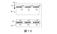
| US15/332,326 US10147702B2 (en) | 2016-10-24 | 2016-10-24 | Method for simultaneously bonding multiple chips of different heights on flexible substrates using anisotropic conductive film or paste |
Publications (3)
| Publication Number | Publication Date |
|---|---|
| JP2018074148A JP2018074148A (ja) | 2018-05-10 |
| JP2018074148A5 JP2018074148A5 (https=) | 2021-03-04 |
| JP6931311B2 true JP6931311B2 (ja) | 2021-09-01 |
Family
ID=60164608
Family Applications (1)
| Application Number | Title | Priority Date | Filing Date |
|---|---|---|---|
| JP2017193915A Expired - Fee Related JP6931311B2 (ja) | 2016-10-24 | 2017-10-04 | 異方性導電膜またはペーストを用いて高さの異なる複数のチップを可撓性基板上に同時に接着する方法 |
Country Status (3)
| Country | Link |
|---|---|
| US (1) | US10147702B2 (https=) |
| EP (2) | EP3312877A3 (https=) |
| JP (1) | JP6931311B2 (https=) |
Families Citing this family (6)
| Publication number | Priority date | Publication date | Assignee | Title |
|---|---|---|---|---|
| DE102015120156B4 (de) * | 2015-11-20 | 2019-07-04 | Semikron Elektronik Gmbh & Co. Kg | Vorrichtung zur materialschlüssigen Verbindung von Verbindungspartnern eines Leistungselekronik-Bauteils und Verwendung einer solchen Vorrichtung |
| JP2020119983A (ja) * | 2019-01-23 | 2020-08-06 | トヨタ自動車株式会社 | 半導体素子接合装置、及び半導体素子接合方法 |
| KR102789194B1 (ko) * | 2020-05-12 | 2025-03-28 | 삼성전자주식회사 | 반도체 칩 실장용 테이프 및 상기 테이프를 이용한 반도체 패키지 제조 방법 |
| TWI786447B (zh) * | 2020-10-15 | 2022-12-11 | 均華精密工業股份有限公司 | 生產設備及預接合裝置 |
| TWI874823B (zh) * | 2021-10-14 | 2025-03-01 | 德商平克塞莫系統有限公司 | 多功能設備和衝壓工具 |
| KR102949513B1 (ko) * | 2023-05-15 | 2026-04-09 | 코스텍시스템(주) | 칩 접합 장비와 이를 포함하는 칩 접합 시스템 및 그 접합 방법 |
Family Cites Families (16)
| Publication number | Priority date | Publication date | Assignee | Title |
|---|---|---|---|---|
| US5353498A (en) * | 1993-02-08 | 1994-10-11 | General Electric Company | Method for fabricating an integrated circuit module |
| US5861678A (en) * | 1997-12-23 | 1999-01-19 | Micron Technology, Inc. | Method and system for attaching semiconductor dice to substrates |
| JP2000150560A (ja) * | 1998-11-13 | 2000-05-30 | Seiko Epson Corp | バンプ形成方法及びバンプ形成用ボンディングツール、半導体ウエーハ、半導体チップ及び半導体装置並びにこれらの製造方法、回路基板並びに電子機器 |
| WO2000045430A1 (en) * | 1999-01-29 | 2000-08-03 | Matsushita Electric Industrial Co., Ltd. | Electronic parts mounting method and device therefor |
| JP2002110744A (ja) * | 2000-09-26 | 2002-04-12 | Matsushita Electric Ind Co Ltd | 半導体実装装置、および半導体実装方法 |
| JP2002198395A (ja) * | 2000-12-26 | 2002-07-12 | Seiko Epson Corp | 半導体装置及びその製造方法、回路基板並びに電子機器 |
| JP4710205B2 (ja) | 2001-09-06 | 2011-06-29 | ソニー株式会社 | フリップチップ実装方法 |
| KR100604334B1 (ko) * | 2003-11-25 | 2006-08-08 | (주)케이나인 | 플립칩 패키징 공정에서 접합력이 향상된 플립칩 접합 방법 |
| US20050282355A1 (en) * | 2004-06-18 | 2005-12-22 | Edwards David N | High density bonding of electrical devices |
| JP4925669B2 (ja) * | 2006-01-13 | 2012-05-09 | ソニーケミカル&インフォメーションデバイス株式会社 | 圧着装置及び実装方法 |
| JP2007294607A (ja) * | 2006-04-24 | 2007-11-08 | Sony Chemical & Information Device Corp | 押圧ヘッド及び押圧装置 |
| KR100785493B1 (ko) * | 2006-05-04 | 2007-12-13 | 한국과학기술원 | 접착제의 수분흡습을 방지하는 플립칩용 웨이퍼 레벨패키지 제조방법 |
| US7884719B2 (en) * | 2006-11-21 | 2011-02-08 | Rcd Technology Inc. | Radio frequency identification (RFID) tag lamination process |
| EP2413676A4 (en) | 2009-03-26 | 2013-03-27 | Sharp Kk | CHIP COMPONENT APPLICATION STRUCTURE, CHIP COMPONENT ATTACHMENT METHOD, AND LIQUID CRYSTAL DISPLAY ARRANGEMENT |
| US8520399B2 (en) * | 2010-10-29 | 2013-08-27 | Palo Alto Research Center Incorporated | Stretchable electronics modules and circuits |
| JP2013084790A (ja) * | 2011-10-11 | 2013-05-09 | Sharp Corp | 熱圧着装置 |
-
2016
- 2016-10-24 US US15/332,326 patent/US10147702B2/en active Active
-
2017
- 2017-10-04 JP JP2017193915A patent/JP6931311B2/ja not_active Expired - Fee Related
- 2017-10-19 EP EP17197418.1A patent/EP3312877A3/en not_active Ceased
- 2017-10-19 EP EP19213869.1A patent/EP3657539A1/en not_active Withdrawn
Also Published As
| Publication number | Publication date |
|---|---|
| JP2018074148A (ja) | 2018-05-10 |
| EP3657539A1 (en) | 2020-05-27 |
| EP3312877A3 (en) | 2018-08-08 |
| US20180114772A1 (en) | 2018-04-26 |
| US10147702B2 (en) | 2018-12-04 |
| EP3312877A2 (en) | 2018-04-25 |
Similar Documents
| Publication | Publication Date | Title |
|---|---|---|
| JP6931311B2 (ja) | 異方性導電膜またはペーストを用いて高さの異なる複数のチップを可撓性基板上に同時に接着する方法 | |
| JP2019015899A (ja) | 表示装置の製造方法、チップ部品の転写方法、および転写部材 | |
| TWI239556B (en) | Reinforcement combining apparatus and method of combining reinforcement | |
| US20070261233A1 (en) | Method and system for fabricating a semiconductor device | |
| US20120018084A1 (en) | Printed Circuit Board Assembly Manufacturing Device And Method | |
| KR0179717B1 (ko) | 반도체 패키지의 제조방법과 반도체의 실장방법 및 반도체 실장장치 | |
| JP2018074148A5 (https=) | ||
| TWI654912B (zh) | Clamping head, mounting device and mounting method using same | |
| JP2015084388A (ja) | 搭載部品収納治具、マルチ部品実装装置およびマルチ部品実装方法 | |
| KR20030012808A (ko) | 반도체 실장체 제조 방법 및 장치 | |
| JP6639915B2 (ja) | 半導体実装装置および半導体実装方法 | |
| TW201036124A (en) | Package structure and manufacturing method thereof | |
| JP7335085B2 (ja) | 転写基板ならびにこれを用いた実装方法および画像表示装置の製造方法 | |
| US6559523B2 (en) | Device for attaching a semiconductor chip to a chip carrier | |
| KR20180038968A (ko) | 첩부 장치 | |
| JP2021141158A (ja) | 素子アレイの加圧装置、製造装置および製造方法 | |
| TW202321040A (zh) | 連接結構體之製造方法 | |
| JP7623788B2 (ja) | 素子アレイの加圧装置、製造装置および製造方法 | |
| CN113690149A (zh) | 一种芯片键合结构、方法及设备 | |
| JP2001189553A (ja) | 基板の接合装置及びその装置を用いた基板の接合方法 | |
| WO2007088647A1 (ja) | 電気部品の実装方法 | |
| CN218996670U (zh) | 转移印章、转移组件和转移设备 | |
| JP5288898B2 (ja) | 接着シートの貼付装置および貼付方法、ならびに電子部品の実装装置および実装方法 | |
| JP2004259917A (ja) | ボンディング方法および装置 | |
| Huttunen et al. | Stretchable LED matrix display |
Legal Events
| Date | Code | Title | Description |
|---|---|---|---|
| RD03 | Notification of appointment of power of attorney |
Free format text: JAPANESE INTERMEDIATE CODE: A7423 Effective date: 20171012 |
|
| RD04 | Notification of resignation of power of attorney |
Free format text: JAPANESE INTERMEDIATE CODE: A7424 Effective date: 20171013 |
|
| A621 | Written request for application examination |
Free format text: JAPANESE INTERMEDIATE CODE: A621 Effective date: 20201002 |
|
| A521 | Request for written amendment filed |
Free format text: JAPANESE INTERMEDIATE CODE: A523 Effective date: 20210125 |
|
| A871 | Explanation of circumstances concerning accelerated examination |
Free format text: JAPANESE INTERMEDIATE CODE: A871 Effective date: 20210125 |
|
| A975 | Report on accelerated examination |
Free format text: JAPANESE INTERMEDIATE CODE: A971005 Effective date: 20210323 |
|
| A131 | Notification of reasons for refusal |
Free format text: JAPANESE INTERMEDIATE CODE: A131 Effective date: 20210401 |
|
| A521 | Request for written amendment filed |
Free format text: JAPANESE INTERMEDIATE CODE: A523 Effective date: 20210630 |
|
| TRDD | Decision of grant or rejection written | ||
| A01 | Written decision to grant a patent or to grant a registration (utility model) |
Free format text: JAPANESE INTERMEDIATE CODE: A01 Effective date: 20210714 |
|
| A61 | First payment of annual fees (during grant procedure) |
Free format text: JAPANESE INTERMEDIATE CODE: A61 Effective date: 20210813 |
|
| R150 | Certificate of patent or registration of utility model |
Ref document number: 6931311 Country of ref document: JP Free format text: JAPANESE INTERMEDIATE CODE: R150 |
|
| LAPS | Cancellation because of no payment of annual fees |