EP3312877A2 - Method and device for simultaneously bonding multiple chips of different heights on a flexible substrate using anisotropic conductive film or paste - Google Patents
Method and device for simultaneously bonding multiple chips of different heights on a flexible substrate using anisotropic conductive film or paste Download PDFInfo
- Publication number
- EP3312877A2 EP3312877A2 EP17197418.1A EP17197418A EP3312877A2 EP 3312877 A2 EP3312877 A2 EP 3312877A2 EP 17197418 A EP17197418 A EP 17197418A EP 3312877 A2 EP3312877 A2 EP 3312877A2
- Authority
- EP
- European Patent Office
- Prior art keywords
- semiconductor chips
- pressure
- flexible substrate
- aca
- multiple semiconductor
- Prior art date
- Legal status (The legal status is an assumption and is not a legal conclusion. Google has not performed a legal analysis and makes no representation as to the accuracy of the status listed.)
- Ceased
Links
Images


Classifications
-
- H—ELECTRICITY
- H01—ELECTRIC ELEMENTS
- H01L—SEMICONDUCTOR DEVICES NOT COVERED BY CLASS H10
- H01L24/00—Arrangements for connecting or disconnecting semiconductor or solid-state bodies; Methods or apparatus related thereto
- H01L24/93—Batch processes
- H01L24/95—Batch processes at chip-level, i.e. with connecting carried out on a plurality of singulated devices, i.e. on diced chips
- H01L24/97—Batch processes at chip-level, i.e. with connecting carried out on a plurality of singulated devices, i.e. on diced chips the devices being connected to a common substrate, e.g. interposer, said common substrate being separable into individual assemblies after connecting
-
- H—ELECTRICITY
- H01—ELECTRIC ELEMENTS
- H01L—SEMICONDUCTOR DEVICES NOT COVERED BY CLASS H10
- H01L24/00—Arrangements for connecting or disconnecting semiconductor or solid-state bodies; Methods or apparatus related thereto
- H01L24/01—Means for bonding being attached to, or being formed on, the surface to be connected, e.g. chip-to-package, die-attach, "first-level" interconnects; Manufacturing methods related thereto
- H01L24/26—Layer connectors, e.g. plate connectors, solder or adhesive layers; Manufacturing methods related thereto
- H01L24/27—Manufacturing methods
-
- H—ELECTRICITY
- H01—ELECTRIC ELEMENTS
- H01L—SEMICONDUCTOR DEVICES NOT COVERED BY CLASS H10
- H01L24/00—Arrangements for connecting or disconnecting semiconductor or solid-state bodies; Methods or apparatus related thereto
- H01L24/74—Apparatus for manufacturing arrangements for connecting or disconnecting semiconductor or solid-state bodies
- H01L24/741—Apparatus for manufacturing means for bonding, e.g. connectors
- H01L24/743—Apparatus for manufacturing layer connectors
-
- H—ELECTRICITY
- H01—ELECTRIC ELEMENTS
- H01L—SEMICONDUCTOR DEVICES NOT COVERED BY CLASS H10
- H01L24/00—Arrangements for connecting or disconnecting semiconductor or solid-state bodies; Methods or apparatus related thereto
- H01L24/74—Apparatus for manufacturing arrangements for connecting or disconnecting semiconductor or solid-state bodies
- H01L24/75—Apparatus for connecting with bump connectors or layer connectors
-
- H—ELECTRICITY
- H01—ELECTRIC ELEMENTS
- H01L—SEMICONDUCTOR DEVICES NOT COVERED BY CLASS H10
- H01L2224/00—Indexing scheme for arrangements for connecting or disconnecting semiconductor or solid-state bodies and methods related thereto as covered by H01L24/00
- H01L2224/01—Means for bonding being attached to, or being formed on, the surface to be connected, e.g. chip-to-package, die-attach, "first-level" interconnects; Manufacturing methods related thereto
- H01L2224/26—Layer connectors, e.g. plate connectors, solder or adhesive layers; Manufacturing methods related thereto
- H01L2224/27—Manufacturing methods
- H01L2224/27001—Involving a temporary auxiliary member not forming part of the manufacturing apparatus, e.g. removable or sacrificial coating, film or substrate
- H01L2224/27003—Involving a temporary auxiliary member not forming part of the manufacturing apparatus, e.g. removable or sacrificial coating, film or substrate for holding or transferring the layer preform
-
- H—ELECTRICITY
- H01—ELECTRIC ELEMENTS
- H01L—SEMICONDUCTOR DEVICES NOT COVERED BY CLASS H10
- H01L2224/00—Indexing scheme for arrangements for connecting or disconnecting semiconductor or solid-state bodies and methods related thereto as covered by H01L24/00
- H01L2224/01—Means for bonding being attached to, or being formed on, the surface to be connected, e.g. chip-to-package, die-attach, "first-level" interconnects; Manufacturing methods related thereto
- H01L2224/26—Layer connectors, e.g. plate connectors, solder or adhesive layers; Manufacturing methods related thereto
- H01L2224/27—Manufacturing methods
- H01L2224/273—Manufacturing methods by local deposition of the material of the layer connector
- H01L2224/2731—Manufacturing methods by local deposition of the material of the layer connector in liquid form
-
- H—ELECTRICITY
- H01—ELECTRIC ELEMENTS
- H01L—SEMICONDUCTOR DEVICES NOT COVERED BY CLASS H10
- H01L2224/00—Indexing scheme for arrangements for connecting or disconnecting semiconductor or solid-state bodies and methods related thereto as covered by H01L24/00
- H01L2224/01—Means for bonding being attached to, or being formed on, the surface to be connected, e.g. chip-to-package, die-attach, "first-level" interconnects; Manufacturing methods related thereto
- H01L2224/26—Layer connectors, e.g. plate connectors, solder or adhesive layers; Manufacturing methods related thereto
- H01L2224/27—Manufacturing methods
- H01L2224/273—Manufacturing methods by local deposition of the material of the layer connector
- H01L2224/2733—Manufacturing methods by local deposition of the material of the layer connector in solid form
- H01L2224/27334—Manufacturing methods by local deposition of the material of the layer connector in solid form using preformed layer
-
- H—ELECTRICITY
- H01—ELECTRIC ELEMENTS
- H01L—SEMICONDUCTOR DEVICES NOT COVERED BY CLASS H10
- H01L2224/00—Indexing scheme for arrangements for connecting or disconnecting semiconductor or solid-state bodies and methods related thereto as covered by H01L24/00
- H01L2224/01—Means for bonding being attached to, or being formed on, the surface to be connected, e.g. chip-to-package, die-attach, "first-level" interconnects; Manufacturing methods related thereto
- H01L2224/26—Layer connectors, e.g. plate connectors, solder or adhesive layers; Manufacturing methods related thereto
- H01L2224/27—Manufacturing methods
- H01L2224/278—Post-treatment of the layer connector
- H01L2224/2783—Reworking, e.g. shaping
-
- H—ELECTRICITY
- H01—ELECTRIC ELEMENTS
- H01L—SEMICONDUCTOR DEVICES NOT COVERED BY CLASS H10
- H01L2224/00—Indexing scheme for arrangements for connecting or disconnecting semiconductor or solid-state bodies and methods related thereto as covered by H01L24/00
- H01L2224/01—Means for bonding being attached to, or being formed on, the surface to be connected, e.g. chip-to-package, die-attach, "first-level" interconnects; Manufacturing methods related thereto
- H01L2224/26—Layer connectors, e.g. plate connectors, solder or adhesive layers; Manufacturing methods related thereto
- H01L2224/27—Manufacturing methods
- H01L2224/278—Post-treatment of the layer connector
- H01L2224/27848—Thermal treatments, e.g. annealing, controlled cooling
-
- H—ELECTRICITY
- H01—ELECTRIC ELEMENTS
- H01L—SEMICONDUCTOR DEVICES NOT COVERED BY CLASS H10
- H01L2224/00—Indexing scheme for arrangements for connecting or disconnecting semiconductor or solid-state bodies and methods related thereto as covered by H01L24/00
- H01L2224/01—Means for bonding being attached to, or being formed on, the surface to be connected, e.g. chip-to-package, die-attach, "first-level" interconnects; Manufacturing methods related thereto
- H01L2224/26—Layer connectors, e.g. plate connectors, solder or adhesive layers; Manufacturing methods related thereto
- H01L2224/28—Structure, shape, material or disposition of the layer connectors prior to the connecting process
- H01L2224/29—Structure, shape, material or disposition of the layer connectors prior to the connecting process of an individual layer connector
- H01L2224/29001—Core members of the layer connector
- H01L2224/29099—Material
- H01L2224/29198—Material with a principal constituent of the material being a combination of two or more materials in the form of a matrix with a filler, i.e. being a hybrid material, e.g. segmented structures, foams
- H01L2224/29199—Material of the matrix
- H01L2224/2929—Material of the matrix with a principal constituent of the material being a polymer, e.g. polyester, phenolic based polymer, epoxy
- H01L2224/29291—The principal constituent being an elastomer, e.g. silicones, isoprene, neoprene
-
- H—ELECTRICITY
- H01—ELECTRIC ELEMENTS
- H01L—SEMICONDUCTOR DEVICES NOT COVERED BY CLASS H10
- H01L2224/00—Indexing scheme for arrangements for connecting or disconnecting semiconductor or solid-state bodies and methods related thereto as covered by H01L24/00
- H01L2224/01—Means for bonding being attached to, or being formed on, the surface to be connected, e.g. chip-to-package, die-attach, "first-level" interconnects; Manufacturing methods related thereto
- H01L2224/26—Layer connectors, e.g. plate connectors, solder or adhesive layers; Manufacturing methods related thereto
- H01L2224/28—Structure, shape, material or disposition of the layer connectors prior to the connecting process
- H01L2224/29—Structure, shape, material or disposition of the layer connectors prior to the connecting process of an individual layer connector
- H01L2224/29001—Core members of the layer connector
- H01L2224/29099—Material
- H01L2224/29198—Material with a principal constituent of the material being a combination of two or more materials in the form of a matrix with a filler, i.e. being a hybrid material, e.g. segmented structures, foams
- H01L2224/29298—Fillers
- H01L2224/29299—Base material
- H01L2224/293—Base material with a principal constituent of the material being a metal or a metalloid, e.g. boron [B], silicon [Si], germanium [Ge], arsenic [As], antimony [Sb], tellurium [Te] and polonium [Po], and alloys thereof
-
- H—ELECTRICITY
- H01—ELECTRIC ELEMENTS
- H01L—SEMICONDUCTOR DEVICES NOT COVERED BY CLASS H10
- H01L2224/00—Indexing scheme for arrangements for connecting or disconnecting semiconductor or solid-state bodies and methods related thereto as covered by H01L24/00
- H01L2224/74—Apparatus for manufacturing arrangements for connecting or disconnecting semiconductor or solid-state bodies and for methods related thereto
- H01L2224/75—Apparatus for connecting with bump connectors or layer connectors
- H01L2224/7525—Means for applying energy, e.g. heating means
- H01L2224/75251—Means for applying energy, e.g. heating means in the lower part of the bonding apparatus, e.g. in the apparatus chuck
-
- H—ELECTRICITY
- H01—ELECTRIC ELEMENTS
- H01L—SEMICONDUCTOR DEVICES NOT COVERED BY CLASS H10
- H01L2224/00—Indexing scheme for arrangements for connecting or disconnecting semiconductor or solid-state bodies and methods related thereto as covered by H01L24/00
- H01L2224/74—Apparatus for manufacturing arrangements for connecting or disconnecting semiconductor or solid-state bodies and for methods related thereto
- H01L2224/75—Apparatus for connecting with bump connectors or layer connectors
- H01L2224/7525—Means for applying energy, e.g. heating means
- H01L2224/753—Means for applying energy, e.g. heating means by means of pressure
- H01L2224/75301—Bonding head
- H01L2224/75312—Material
-
- H—ELECTRICITY
- H01—ELECTRIC ELEMENTS
- H01L—SEMICONDUCTOR DEVICES NOT COVERED BY CLASS H10
- H01L2224/00—Indexing scheme for arrangements for connecting or disconnecting semiconductor or solid-state bodies and methods related thereto as covered by H01L24/00
- H01L2224/74—Apparatus for manufacturing arrangements for connecting or disconnecting semiconductor or solid-state bodies and for methods related thereto
- H01L2224/75—Apparatus for connecting with bump connectors or layer connectors
- H01L2224/7525—Means for applying energy, e.g. heating means
- H01L2224/753—Means for applying energy, e.g. heating means by means of pressure
- H01L2224/75301—Bonding head
- H01L2224/75314—Auxiliary members on the pressing surface
- H01L2224/75315—Elastomer inlay
- H01L2224/75316—Elastomer inlay with retaining mechanisms
-
- H—ELECTRICITY
- H01—ELECTRIC ELEMENTS
- H01L—SEMICONDUCTOR DEVICES NOT COVERED BY CLASS H10
- H01L2224/00—Indexing scheme for arrangements for connecting or disconnecting semiconductor or solid-state bodies and methods related thereto as covered by H01L24/00
- H01L2224/74—Apparatus for manufacturing arrangements for connecting or disconnecting semiconductor or solid-state bodies and for methods related thereto
- H01L2224/75—Apparatus for connecting with bump connectors or layer connectors
- H01L2224/7525—Means for applying energy, e.g. heating means
- H01L2224/753—Means for applying energy, e.g. heating means by means of pressure
- H01L2224/75301—Bonding head
- H01L2224/75314—Auxiliary members on the pressing surface
- H01L2224/75318—Shape of the auxiliary member
-
- H—ELECTRICITY
- H01—ELECTRIC ELEMENTS
- H01L—SEMICONDUCTOR DEVICES NOT COVERED BY CLASS H10
- H01L2224/00—Indexing scheme for arrangements for connecting or disconnecting semiconductor or solid-state bodies and methods related thereto as covered by H01L24/00
- H01L2224/74—Apparatus for manufacturing arrangements for connecting or disconnecting semiconductor or solid-state bodies and for methods related thereto
- H01L2224/75—Apparatus for connecting with bump connectors or layer connectors
- H01L2224/7525—Means for applying energy, e.g. heating means
- H01L2224/753—Means for applying energy, e.g. heating means by means of pressure
- H01L2224/75301—Bonding head
- H01L2224/75314—Auxiliary members on the pressing surface
- H01L2224/7532—Material of the auxiliary member
-
- H—ELECTRICITY
- H01—ELECTRIC ELEMENTS
- H01L—SEMICONDUCTOR DEVICES NOT COVERED BY CLASS H10
- H01L2224/00—Indexing scheme for arrangements for connecting or disconnecting semiconductor or solid-state bodies and methods related thereto as covered by H01L24/00
- H01L2224/74—Apparatus for manufacturing arrangements for connecting or disconnecting semiconductor or solid-state bodies and for methods related thereto
- H01L2224/75—Apparatus for connecting with bump connectors or layer connectors
- H01L2224/758—Means for moving parts
- H01L2224/75821—Upper part of the bonding apparatus, i.e. bonding head
- H01L2224/75824—Translational mechanism
-
- H—ELECTRICITY
- H01—ELECTRIC ELEMENTS
- H01L—SEMICONDUCTOR DEVICES NOT COVERED BY CLASS H10
- H01L2224/00—Indexing scheme for arrangements for connecting or disconnecting semiconductor or solid-state bodies and methods related thereto as covered by H01L24/00
- H01L2224/74—Apparatus for manufacturing arrangements for connecting or disconnecting semiconductor or solid-state bodies and for methods related thereto
- H01L2224/75—Apparatus for connecting with bump connectors or layer connectors
- H01L2224/7598—Apparatus for connecting with bump connectors or layer connectors specially adapted for batch processes
-
- H—ELECTRICITY
- H01—ELECTRIC ELEMENTS
- H01L—SEMICONDUCTOR DEVICES NOT COVERED BY CLASS H10
- H01L2224/00—Indexing scheme for arrangements for connecting or disconnecting semiconductor or solid-state bodies and methods related thereto as covered by H01L24/00
- H01L2224/80—Methods for connecting semiconductor or other solid state bodies using means for bonding being attached to, or being formed on, the surface to be connected
- H01L2224/83—Methods for connecting semiconductor or other solid state bodies using means for bonding being attached to, or being formed on, the surface to be connected using a layer connector
- H01L2224/8312—Aligning
- H01L2224/83121—Active alignment, i.e. by apparatus steering, e.g. optical alignment using marks or sensors
-
- H—ELECTRICITY
- H01—ELECTRIC ELEMENTS
- H01L—SEMICONDUCTOR DEVICES NOT COVERED BY CLASS H10
- H01L2224/00—Indexing scheme for arrangements for connecting or disconnecting semiconductor or solid-state bodies and methods related thereto as covered by H01L24/00
- H01L2224/80—Methods for connecting semiconductor or other solid state bodies using means for bonding being attached to, or being formed on, the surface to be connected
- H01L2224/83—Methods for connecting semiconductor or other solid state bodies using means for bonding being attached to, or being formed on, the surface to be connected using a layer connector
- H01L2224/8319—Arrangement of the layer connectors prior to mounting
- H01L2224/83192—Arrangement of the layer connectors prior to mounting wherein the layer connectors are disposed only on another item or body to be connected to the semiconductor or solid-state body
-
- H—ELECTRICITY
- H01—ELECTRIC ELEMENTS
- H01L—SEMICONDUCTOR DEVICES NOT COVERED BY CLASS H10
- H01L2224/00—Indexing scheme for arrangements for connecting or disconnecting semiconductor or solid-state bodies and methods related thereto as covered by H01L24/00
- H01L2224/80—Methods for connecting semiconductor or other solid state bodies using means for bonding being attached to, or being formed on, the surface to be connected
- H01L2224/83—Methods for connecting semiconductor or other solid state bodies using means for bonding being attached to, or being formed on, the surface to be connected using a layer connector
- H01L2224/832—Applying energy for connecting
- H01L2224/83201—Compression bonding
- H01L2224/83203—Thermocompression bonding, e.g. diffusion bonding, pressure joining, thermocompression welding or solid-state welding
-
- H—ELECTRICITY
- H01—ELECTRIC ELEMENTS
- H01L—SEMICONDUCTOR DEVICES NOT COVERED BY CLASS H10
- H01L2224/00—Indexing scheme for arrangements for connecting or disconnecting semiconductor or solid-state bodies and methods related thereto as covered by H01L24/00
- H01L2224/80—Methods for connecting semiconductor or other solid state bodies using means for bonding being attached to, or being formed on, the surface to be connected
- H01L2224/83—Methods for connecting semiconductor or other solid state bodies using means for bonding being attached to, or being formed on, the surface to be connected using a layer connector
- H01L2224/838—Bonding techniques
- H01L2224/8385—Bonding techniques using a polymer adhesive, e.g. an adhesive based on silicone, epoxy, polyimide, polyester
- H01L2224/83851—Bonding techniques using a polymer adhesive, e.g. an adhesive based on silicone, epoxy, polyimide, polyester being an anisotropic conductive adhesive
-
- H—ELECTRICITY
- H01—ELECTRIC ELEMENTS
- H01L—SEMICONDUCTOR DEVICES NOT COVERED BY CLASS H10
- H01L2224/00—Indexing scheme for arrangements for connecting or disconnecting semiconductor or solid-state bodies and methods related thereto as covered by H01L24/00
- H01L2224/80—Methods for connecting semiconductor or other solid state bodies using means for bonding being attached to, or being formed on, the surface to be connected
- H01L2224/83—Methods for connecting semiconductor or other solid state bodies using means for bonding being attached to, or being formed on, the surface to be connected using a layer connector
- H01L2224/838—Bonding techniques
- H01L2224/8385—Bonding techniques using a polymer adhesive, e.g. an adhesive based on silicone, epoxy, polyimide, polyester
- H01L2224/83855—Hardening the adhesive by curing, i.e. thermosetting
- H01L2224/83862—Heat curing
-
- H—ELECTRICITY
- H01—ELECTRIC ELEMENTS
- H01L—SEMICONDUCTOR DEVICES NOT COVERED BY CLASS H10
- H01L2224/00—Indexing scheme for arrangements for connecting or disconnecting semiconductor or solid-state bodies and methods related thereto as covered by H01L24/00
- H01L2224/93—Batch processes
- H01L2224/95—Batch processes at chip-level, i.e. with connecting carried out on a plurality of singulated devices, i.e. on diced chips
- H01L2224/95053—Bonding environment
- H01L2224/95091—Under pressure
-
- H—ELECTRICITY
- H01—ELECTRIC ELEMENTS
- H01L—SEMICONDUCTOR DEVICES NOT COVERED BY CLASS H10
- H01L2224/00—Indexing scheme for arrangements for connecting or disconnecting semiconductor or solid-state bodies and methods related thereto as covered by H01L24/00
- H01L2224/93—Batch processes
- H01L2224/95—Batch processes at chip-level, i.e. with connecting carried out on a plurality of singulated devices, i.e. on diced chips
- H01L2224/9512—Aligning the plurality of semiconductor or solid-state bodies
- H01L2224/95121—Active alignment, i.e. by apparatus steering
-
- H—ELECTRICITY
- H01—ELECTRIC ELEMENTS
- H01L—SEMICONDUCTOR DEVICES NOT COVERED BY CLASS H10
- H01L2224/00—Indexing scheme for arrangements for connecting or disconnecting semiconductor or solid-state bodies and methods related thereto as covered by H01L24/00
- H01L2224/93—Batch processes
- H01L2224/95—Batch processes at chip-level, i.e. with connecting carried out on a plurality of singulated devices, i.e. on diced chips
- H01L2224/97—Batch processes at chip-level, i.e. with connecting carried out on a plurality of singulated devices, i.e. on diced chips the devices being connected to a common substrate, e.g. interposer, said common substrate being separable into individual assemblies after connecting
-
- H—ELECTRICITY
- H01—ELECTRIC ELEMENTS
- H01L—SEMICONDUCTOR DEVICES NOT COVERED BY CLASS H10
- H01L24/00—Arrangements for connecting or disconnecting semiconductor or solid-state bodies; Methods or apparatus related thereto
- H01L24/01—Means for bonding being attached to, or being formed on, the surface to be connected, e.g. chip-to-package, die-attach, "first-level" interconnects; Manufacturing methods related thereto
- H01L24/26—Layer connectors, e.g. plate connectors, solder or adhesive layers; Manufacturing methods related thereto
- H01L24/28—Structure, shape, material or disposition of the layer connectors prior to the connecting process
- H01L24/29—Structure, shape, material or disposition of the layer connectors prior to the connecting process of an individual layer connector
-
- H—ELECTRICITY
- H01—ELECTRIC ELEMENTS
- H01L—SEMICONDUCTOR DEVICES NOT COVERED BY CLASS H10
- H01L24/00—Arrangements for connecting or disconnecting semiconductor or solid-state bodies; Methods or apparatus related thereto
- H01L24/80—Methods for connecting semiconductor or other solid state bodies using means for bonding being attached to, or being formed on, the surface to be connected
- H01L24/83—Methods for connecting semiconductor or other solid state bodies using means for bonding being attached to, or being formed on, the surface to be connected using a layer connector
Definitions
- the present disclosure relates to packaging of electronic components, more particularly to the bonding of semiconductor chips to a flexible substrate.
- Flexible hybrid electronics integrates packaged electronic components with high precision digital printing technologies on low cost flexible substrates and provides a cost-effective, large-area manufacturing technique while keeping the same complex functionality and processing capability as conventional integrated circuits.
- Various techniques have been developed for semiconductor chip integration on flexible substrates. In this process semiconductor chips are attached or bonded individually to conductive traces on the substrate. Bonding equipment consists of a metal thermode or hot bar supplying heat and pressure to bond a single semiconductor chip.
- Bonding equipment consists of a metal thermode or hot bar supplying heat and pressure to bond a single semiconductor chip.
- this technique does not allow for the attachment or bonding of multiple chips of arbitrary height in a dense configuration during the same attachment or bonding operation, i.e., the attachment or bonding does not take place in a substantially simultaneous manner. This restriction reduces the throughput for the semiconductor chip attachment or bonding step. Additionally, subsequent attachment or bonding of adjacent semiconductor chips can act to distort the thermally sensitive polymer substrate being used.
- the present application provides a method and system for simultaneously bonding multiple semiconductor chips of different height profiles on a flexible substrate.
- a method includes providing a flexible substrate with printed conductive traces. Placing an anisotropic conductive adhesive (ACA) over at least portions of the printed conductive traces of the flexible substrate, the ACA including a thermosetting adhesive and conductive spherical elements. Next the ACA is tacked in place by application of heat and pressure for a predetermined time. Thereafter a first side of each of multiple semiconductor chips is positioned to align with selected locations of the printed conductive traces of the flexible substrate lying under the ACA. At least one of the multiple semiconductor chips has a height profile different from at least one other one of the multiple semiconductor chips.
- ACA anisotropic conductive adhesive
- thermosetting adhesive of the ACA by applying heat and pressure.
- the pressure is also applied to a second side of each of the multiple semiconductor chips, and the applying of the pressure presses and deforms the conductive spherical elements of the ACA, wherein electrical contact is made between the semiconductor chips and at least portions of the printed conductive traces.
- the application of pressure occurs on a second side of each of the multiple semiconductor chips opposite the first side of each of the multiple semiconductor chips.
- applying the pressure includes using a pressure applying device having a deformable bonding head to provide the application of pressure to the second side of each of the multiple semiconductor chips, wherein the semiconductor chips of differing heights deform the deformable bonding head of the pressure applying device by different amounts of compression.
- the deformable bonding head is a rubber or other compliant material capable of withstanding a required bonding temperature and with a hardness to conform to the profiles of the semiconductor chips.
- the deformable bonding head is moved by at least one of a gas cylinder mechanism and a hydraulic mechanism.
- applying the pressure includes using a pressure applying device having an expandable elastic membrane to provide the application of pressure to the second side of each of the multiple semiconductor chips, wherein the expandable elastic membrane conforms to profiles of the semiconductor chips of differing heights that are to be bonded.
- applying the pressure includes using a pressure applying device having (i) a pin screen with a plurality of movable pins spaced apart from each other, each of the pins having a first end and a second end, (ii) a deformable elastic material located adjacent the first ends of the pins and second ends of the pins located at one of adjacent to and in contact with a second surface of each of the multiple semiconductor chips, and (iii) a pressure applicator which moves the pins into contact with the second side of each of the multiple semiconductor chips, wherein as the pins come into contact with the second side of each of the semiconductor chips the first ends of the corresponding pins deform the elastic plug.
- applying of pressure includes using a pressure applying device having (i) a pin screen with a plurality of movable pins spaced apart from each other, each of the pins having a first end and a second end, (ii) an expandable elastic membrane located adjacent the first ends of the pins and second end of the pins located at one of adjacent to and in contact with a second surface of each of the multiple semiconductor chips, and (iii) a pressure applicator which moves the pins towards or into contact with the second side of each of the multiple semiconductor chips, wherein as the pins come into contact with the second side of each of the semiconductor chips the first end of the corresponding pins deform the expandable elastic membrane.
- the present application also discloses a semiconductor chip bonding device for bonding multiple semiconductor chips, at least one of the semiconductor chips having a height profile different from at least one other one of the multiple semiconductor chips.
- the device includes a heat generating element configured to hold a flexible substrate having printed conductive traces, the printed conductive traces at least partially covered by an anisotropic conductive adhesive.
- a semiconductor chip pick and place device is used to position a first side of each of the multiple semiconductor chips onto selected portions of the flexible substrate, wherein the semiconductor chip pick and place device is further configured to locate the semiconductor chips in an desired manner in relationship to the printed conductive traces.
- a pressure application arrangement includes a semiconductor chip engagement arrangement, wherein the pressure application arrangement is in an operational position sufficient to allow the semiconductor chip engagement arrangement to engage with a second surface of each of the semiconductor chips located on the flexible substrate, wherein at least one of the semiconductor chips has a height profile different from at least one other one of the multiple semiconductor chips.
- the semiconductor chip engagement element is a deformable bonding head, wherein the semiconductor chips of differing heights deform the deformable bonding head by different amounts of compression.
- the pressure application arrangement includes at least one of a gas cylinder mechanism and a hydraulic mechanism.
- the semiconductor chip engagement element is an expandable elastic membrane to which gas pressure is applied to provide the application of pressure to the second side of each of the multiple semiconductor chips, wherein the expandable elastic membrane conforms to the profiles of the semiconductor chips of different heights.
- the semiconductor chip engagement element includes (i) a pin screen with a plurality of movable pins spaced apart from each other, each of the pins having a first end and a second end, (ii) a deformable bonding head located adjacent the first ends of the pins, and the second end of the pins located at one of adjacent and in contact with a second surface of each of the multiple semiconductor chips, and (iii) a pressure applicator which moves the pins into contact with the second side of each of the multiple semiconductor chips, wherein as the pins come into contact with the second side of each of the semiconductor chips the first end of the corresponding pins deform the bonding head.
- the semiconductor chip engagement element includes (i) a pin screen with a plurality of movable pins spaced apart from each other, each of the pins having a first end and a second end, (ii) an expandable elastic membrane located adjacent the first ends of the pins and the second end of the pins located at one of adjacent and in contact with a second surface of each of the multiple semiconductor chips, and (iii) a pressure applicator which moves the pins towards or into contact with the second side of each of the multiple semiconductor chips, wherein as the pins come into contact with the second side of each of the semiconductor chips the first end of the corresponding pins the expandable elastic membrane.
- a fluoropolymer film is applied to a surface of the semiconductor chip engagement arrangement, to avoid a sticking of the bonding head to the semiconductor chips.
- a minimum height difference profile between at least two of the multiple semiconductor chips is 0.5 mm.
- a minimum height difference profile between at least two of the multiple semiconductor chips is 1.0 mm.
- the present disclosure provides methods, systems and equipment to facilitate high density attachment or bonding of multiple semiconductor chips having different heights, where the attachment or bonding is done in a substantially simultaneous manner.
- ACA anisotropic conductive adhesive
- ACF anisotropic conductive film
- ACP anisotropic conductive paste
- FIGURE 1A shows a top and side view of a flexible substrate 100 , having a upper surface 100A , and a lower surface 100B , including conductive traces 102 , which are commonly applied by printing techniques. It is understood that other techniques may also be employed to obtain the conductive traces. Further the flexible substrate and conductive traces of FIGURE 1A are depicted in a simplified form for convenience of discussion, and it is to be appreciated that the present concepts are applicable to much more complex designs and layouts as known in the art.
- an anisotropic conductive adhesive (ACA) 104 is provided to cover at least some of the printed conductive traces 102 .
- the anisotropic conductive adhesive (ACA) is in the form of an anisotropic conductive film (ACF) or an anisotropic conductive paste (ACP).
- ACF anisotropic conductive film
- ACP anisotropic conductive paste
- the application of the ACA in either form may be achieved by an adhesive dispenser 106 which is understood to be a film dispenser, paste dispenser, or other appropriate dispensing configuration.
- the ACA e.g., tape, in one embodiment
- element 108 is a thermode or hot bar.
- element 108 is configured to move in the direction of arrow 110 moves down to the surface 100A of the flexible substrate 100 and may come into contact with the material on its surface.
- the heat and pressure may be applied for a determined time, such as a few seconds (in one embodiment 1-3 seconds, where 3-5 seconds is typical) to obtain the tacking state for the anisotropic conductive adhesive.
- the elements 102 , 104 are shown in the bottom Figure of 1C as dashed to note the view is from under element 108 .
- anisotropic conductive adhesive When the anisotropic conductive adhesive is in the form of an anisotropic conductive tape (ACT), it will commonly have a non-sticking liner on its outer upper surface. Following the tacking operation, this liner may be removed.
- ACT anisotropic conductive tape
- FIGURE 1D the flexible substrate 100 is shown with the conductive traces 102 covered by the anisotropic conductive adhesive (ACA) 104 in a tacky state 104A .
- ACA anisotropic conductive adhesive
- FIGURE 1E Thereafter and with attention to top and side views of FIGURE 1E shown is a semiconductor chip pick and place device 112 operating in cooperation with a semiconductor chip holding area 114 having a plurality of semiconductor chips 116A and 116B .
- the pick and place device 112 selects one or more semiconductor chips 116 and thereafter moves such selected chips to the flexible substrate 100 .
- the semiconductor chips 116A and 116B are positioned and oriented by the pick and place device 112 so that they are registered, i.e., properly positioned with selected areas of the conductive printed traces 102 , where the traces lie under the tacky anisotropic conductive adhesive 104A .
- pick and place device 112 is shown with a carrying element 112A carrying two semiconductor chips 116A and 116B , which are positioned such that the semiconductor chips 116A , 116B will be placed to bridge areas of the conductive traces (not shown) covered by the ACA in a tacky state.
- FIGURE 1E depicts the semiconductor chips 116A and 116B having different height profiles.
- FIGURE 1E show the pick and place device placing two semiconductor chips at the same time, in certain embodiments only a single semiconductor chip is picked and placed at a time. While in other embodiments multiple semiconductor chips are picked and placed at the same time. It is also to be appreciated that it is common for more than a single pick and place device to be used in populating a flexible substrate.
- semiconductor chips 116A , 116B having distinctly different height profiles are positioned on the upper surface 100A of the flexible substrate 100 .
- attachment and/or bonding of these semiconductor chips would be undertaken one at a time due to the height differences, and therefore a substantially simultaneous attachment or bonding operation would not be achieved, slowing down the packaging operations.
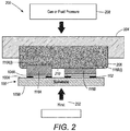
- FIGURE 2 depicted is a side view of an attachment or bonding device 200 designed to bond multiple chips of different heights in a dense configuration.
- the device 200 is being shown in use with the previously illustrated arrangement which includes the flexible substrate 100 , which has the conductive traces 102 covered by the ACA (e.g ., in certain embodiments being an ACF and/or ACP) 104 (in a tacky state 104A ) and which carries semiconductor chips of differing heights 116A , 116B .
- the arrangement is in operational arrangement with heater (e.g., a heated platen) 202 positioned adjacent the second surface 100B of the flexible substrate 100 .
- heater e.g., a heated platen
- the attachment or bonding device 200 further includes a support member 204 to which is attached a bonding head (also called herein compliant plug, of rubber or other polymer) 206 .
- a movement element (which may be in the form of an gas (e.g., air) cylinder mechanism, hydraulic mechanism, or other appropriate motivating arrangement) 208 is in operational position to move the support member 204 and therefore the bonding head 206 into association with upper surface 116A(i) of semiconductor chip 116A and an upper surface 116B(i) of semiconductor chip 116B .
- thermosetting adhesive of the ACA As the movement element 208 is activated to move the support member 204 and bonding head 206 into contact with the semiconductor chips 116A, 116B , heat from the heated platen 202 and pressure from the upper portion of the attachment or bonding device 200 apply heat and pressure, thereby curing the thermosetting adhesive of the ACA while simultaneously pressing and deforming spherical elements (conductive balls) and at substantially the same time curing of the thermosetting adhesive is taking place.
- An appropriate force factor for the movement element (i.e., in the form of an air cylinder or hydraulic cylinder) 208 allows for the use of standard levels of air pressure and/or hydraulic pressure to achieve very large forces on the semiconductor chips.
- the force factor will depend on the pressure that needs to be applied and that is proportional to the total area of the semiconductor chips being bonded.
- a typical upper level of useful air pressure is about 80 psi.
- an air cylinder with a force factor of 3 (which gives a maximum applied pressure of 240 psi) was used. This can be increased if a large number of chips are being bonded.
- a fluoropolymer film 210 is, in certain embodiments, applied to the surface of the bonding head 206 to diminish or prevent sticking of the semiconductor chips 116A , 116B to the bonding head 206 when the pressure is removed.
- the tacky ACA 104A of FIGURE 2 is shown extending across a gap between traces 102 . This is provided as one possibility if the tackiness has a sufficient stiffness. In other embodiments, the tacky ACA would encompass the semiconductor chips but not the gap area (similar concepts are also appropriate for FIGURES 3 , 4 , and 5 ).
- a particular aspect of attachment or bonding device 200 is that the bonding head 206 is compliant and allows for deformation when downward pressure is applied causing a meeting with the top surfaces 116A , 116B .
- the semiconductor chip 116A acts to deform the bonding head to a greater degree than the semiconductor chip 116B which has a lower height profile than semiconductor chip 116A .
- a neoprene rubber may be used as the bonding head (i.e., compliant plug) 206 .
- a material of 40A hardness was found to be useful for the present operation. It is understood that a softer rubber would tend to be more useful when there is a greater disparity in height of the semiconductor chips being bonded. For a large enough disparity in height there will be significant differences in the compressive force being applied to different height chips because of the difference in the amount of compression of the rubber over each chip.
- FIGURE 3 illustrated is an alternative multiple semiconductor chip attachment or bonding device 300 . While the materials on the flexible substrate 100 are similar to those discussed in connection with FIGURE 2 as well as the flexible substrate 100 being operationally associated with a heated platen 202 , the pressure providing mechanism for the top of the semiconductor chips 116A and 116B is implemented in a different manner. More particularly, support members 302A , 302B hold an expandable elastic membrane 304 which, in certain embodiments, may be, but is not limited to approximately 1/8 inch thick.
- attachment or bonding device 300 is also shown in attachment or bonding device 300 .
- a movement element 306 similar to that discussed in connection with FIGURE 2 .
- the actual implementation may be slightly different as the pressure is being applied to the expandable elastic membrane 304 rather than to a non-flexible support member or carrier (e.g., 204 of FIGURE 2 ).
- the arrangement to move the expandable elastic membrane 304 may be a gas (e.g., air) cylinder mechanism, a hydraulic mechanism, or other appropriate motivating arrangement. More particularly, this motivating force (gas pressure or fluid pressure) is directly applied to the expandable elastic membrane 304 which pushes the membrane down and causes it to conform to the profiles of the semiconductor chips to be attached or bonded. Similar to the concepts in FIGURE 2 , for the taller semiconductor chip 106a , there will be more of an impediment to the movement of the expandable elastic membrane 304 downward. However, each semiconductor chip will engage with the expandable elastic membrane 304. By this arrangement heat and pressure is thereby applied to the flexible substrate arrangement 100 resulting in an attachment or bonding of the semiconductor chips 116A and 116B .
- gas e.g., air
- hydraulic mechanism e.g., hydraulic mechanism
- FIGURE 4 illustrated is a further embodiment of an attachment or bonding device 400 .
- a flexible substrate 100 and associated elements previously discussed e.g., conductive traces 102 , tacky ACA 104A , semiconductor chips 116A , 116B
- a heated platen 202 such as in the previous embodiments is also provided.
- Distinguishing characteristics of attachment or bonding device 400 is in the use of a plurality of pins held in a support structure (e.g., a pin screen) 404 in a manner that allows the pins to move transversely back and forth, particularly when pressure is applied at ends 402A of pins 402 .
- an elastic plug 406 is provided (in certain embodiments made of a rubber or other polymer).
- a carrying mechanism 408 which is movable. As the carrying mechanism 408 moves downward towards the top surfaces of semiconductor chips 116A , 116B , the pin ends 402A come into contact with the top surfaces of the semiconductor chips 116A , 116B . This causes the pins 402 to be pushed back into the elastic plug 406 .
- the deformability and strength of the elastic plug 406 is selected such that sufficient pressure is provided on the top surface of the semiconductor chips 116A , 116B that as heat is supplied by heater (e.g., heat platen) 202 , the bonding of the chips take place in a substantially simultaneous manner, even though semiconductor chips 116A and 116B have different height profiles.
- FIGURE 5 depicted is yet another embodiment using the pin screen type structure.
- the attachment or bonding device 500 again is similarly arranged to operate with the previously discussed flexible substrate 100 , conductive traces 102 , tacky ACA 104A , and semiconductor chips 116A , 116B .
- a heated platen 202 is provided on a bottom side surface of the flexible substrate 100 .
- an elastic membrane 502 is provided which is secured at ends 504A , 504B .
- the pins 506 again arranged to be securely movable within a holding region 508 , being able to translate movement depending on pressure applied to the tips 506A of pins 506 .
- a gas e.g., air
- hydraulic or other appropriate source of pressure 510 is provided on one side of membrane 502 .
- the pressure (such as similarly discussed in connection with the previous embodiments) is applied causing the membrane to move in a downward direction, such as by arrow 512 , the pins move into contact with the upper surfaces of semiconductor chips 116A , 116B and the membrane 502 supplies the pressure to the semiconductor chips 116A , 116B such that pressure and heat are sufficient to perform the attachment or bonding process in a simultaneous manner.
- FIGURE 6A illustrated are two semiconductor chips (e.g ., resistors) having two different height components such as semiconductor chip 602 being 1.75 mm and semiconductor chip 604 being 0.6 mm. These chips have been bonded with the use of ACF to conductive traces as discussed in the previous examples. In other words, they have been bonded in a simultaneous bonding operation even though they have significant different height components.
- semiconductor chip 602 being 1.75 mm
- semiconductor chip 604 being 0.6 mm.
- These chips have been bonded with the use of ACF to conductive traces as discussed in the previous examples. In other words, they have been bonded in a simultaneous bonding operation even though they have significant different height components.
- FIGURE 6B illustrates two resistors 610 , 612 bound side-by-side in a high density close proximity configuration using the concepts of the present application. It is understood that the present application teaches methods and processed as well as systems and devices that allow for a substantially simultaneous bonding for attachment of semiconductor chips having intentionally different distinct height profiles. This is an aspect which is particularly suitable for packing of hybrid electronics on flexible substrates.
Landscapes
- Engineering & Computer Science (AREA)
- Computer Hardware Design (AREA)
- Microelectronics & Electronic Packaging (AREA)
- Power Engineering (AREA)
- Manufacturing & Machinery (AREA)
- Wire Bonding (AREA)
- Electric Connection Of Electric Components To Printed Circuits (AREA)
- Adhesives Or Adhesive Processes (AREA)
Abstract
providing a flexible substrate (100) with printed conductive traces (102);
placing an anisotropic conductive adhesive (ACA) (104) over at least portions of the printed conductive traces (102) of the flexible substrate (100), the ACA (104) including a thermosetting adhesive and conductive spherical elements;
tacking the ACA (104) in place by application of heat and pressure for a predetermined time;
positioning and orientating a first side of each of multiple semiconductor chips (116A, 116B) to align with selected locations of the printed conductive traces (102) of the flexible substrate (100) lying under the ACA (104), wherein at least one of the multiple semiconductor chips (116A, 116B) has a height profile different from at least one other one of the multiple semiconductor chips (116A, 116B);
curing the thermosetting adhesive of the ACA (104) by applying heat and pressure, wherein the pressure is applied, with a deformable bonding head (206), an expandable elastic membrane (304) or a plurality of movable pins (402) held in a support structure (e.g., a pin screen) (404), to a second side of each of the multiple semiconductor chips (116A, 116B), the applying of the pressure pressing and deforming the conductive spherical elements of the ACA (104), wherein electrical contact is made between the semiconductor chips (116A, 116B) and at least portions of the printed conductive traces (102).
Description
- The present disclosure relates to packaging of electronic components, more particularly to the bonding of semiconductor chips to a flexible substrate.
- Flexible hybrid electronics integrates packaged electronic components with high precision digital printing technologies on low cost flexible substrates and provides a cost-effective, large-area manufacturing technique while keeping the same complex functionality and processing capability as conventional integrated circuits. Various techniques have been developed for semiconductor chip integration on flexible substrates. In this process semiconductor chips are attached or bonded individually to conductive traces on the substrate. Bonding equipment consists of a metal thermode or hot bar supplying heat and pressure to bond a single semiconductor chip. However use of this technique does not allow for the attachment or bonding of multiple chips of arbitrary height in a dense configuration during the same attachment or bonding operation, i.e., the attachment or bonding does not take place in a substantially simultaneous manner. This restriction reduces the throughput for the semiconductor chip attachment or bonding step. Additionally, subsequent attachment or bonding of adjacent semiconductor chips can act to distort the thermally sensitive polymer substrate being used.
- Therefore, it is considered desirable to develop a method, system and equipment to facilitate high density attachment of semiconductor chips having different heights substantially simultaneously.
- The present application provides a method and system for simultaneously bonding multiple semiconductor chips of different height profiles on a flexible substrate. Such a method includes providing a flexible substrate with printed conductive traces. Placing an anisotropic conductive adhesive (ACA) over at least portions of the printed conductive traces of the flexible substrate, the ACA including a thermosetting adhesive and conductive spherical elements. Next the ACA is tacked in place by application of heat and pressure for a predetermined time. Thereafter a first side of each of multiple semiconductor chips is positioned to align with selected locations of the printed conductive traces of the flexible substrate lying under the ACA. At least one of the multiple semiconductor chips has a height profile different from at least one other one of the multiple semiconductor chips. Next there is a curing of the thermosetting adhesive of the ACA by applying heat and pressure. The pressure is also applied to a second side of each of the multiple semiconductor chips, and the applying of the pressure presses and deforms the conductive spherical elements of the ACA, wherein electrical contact is made between the semiconductor chips and at least portions of the printed conductive traces.
- In another aspect the application of pressure occurs on a second side of each of the multiple semiconductor chips opposite the first side of each of the multiple semiconductor chips.
- In another aspect applying the pressure includes using a pressure applying device having a deformable bonding head to provide the application of pressure to the second side of each of the multiple semiconductor chips, wherein the semiconductor chips of differing heights deform the deformable bonding head of the pressure applying device by different amounts of compression.
- In another aspect the deformable bonding head is a rubber or other compliant material capable of withstanding a required bonding temperature and with a hardness to conform to the profiles of the semiconductor chips.
- In another aspect the deformable bonding head is moved by at least one of a gas cylinder mechanism and a hydraulic mechanism.
- In another aspect applying the pressure includes using a pressure applying device having an expandable elastic membrane to provide the application of pressure to the second side of each of the multiple semiconductor chips, wherein the expandable elastic membrane conforms to profiles of the semiconductor chips of differing heights that are to be bonded.
- In another aspect applying the pressure includes using a pressure applying device having (i) a pin screen with a plurality of movable pins spaced apart from each other, each of the pins having a first end and a second end, (ii) a deformable elastic material located adjacent the first ends of the pins and second ends of the pins located at one of adjacent to and in contact with a second surface of each of the multiple semiconductor chips, and (iii) a pressure applicator which moves the pins into contact with the second side of each of the multiple semiconductor chips, wherein as the pins come into contact with the second side of each of the semiconductor chips the first ends of the corresponding pins deform the elastic plug.
- In another aspect applying of pressure includes using a pressure applying device having (i) a pin screen with a plurality of movable pins spaced apart from each other, each of the pins having a first end and a second end, (ii) an expandable elastic membrane located adjacent the first ends of the pins and second end of the pins located at one of adjacent to and in contact with a second surface of each of the multiple semiconductor chips, and (iii) a pressure applicator which moves the pins towards or into contact with the second side of each of the multiple semiconductor chips, wherein as the pins come into contact with the second side of each of the semiconductor chips the first end of the corresponding pins deform the expandable elastic membrane.
- The present application also discloses a semiconductor chip bonding device for bonding multiple semiconductor chips, at least one of the semiconductor chips having a height profile different from at least one other one of the multiple semiconductor chips. The device includes a heat generating element configured to hold a flexible substrate having printed conductive traces, the printed conductive traces at least partially covered by an anisotropic conductive adhesive. A semiconductor chip pick and place device is used to position a first side of each of the multiple semiconductor chips onto selected portions of the flexible substrate, wherein the semiconductor chip pick and place device is further configured to locate the semiconductor chips in an desired manner in relationship to the printed conductive traces. A pressure application arrangement includes a semiconductor chip engagement arrangement, wherein the pressure application arrangement is in an operational position sufficient to allow the semiconductor chip engagement arrangement to engage with a second surface of each of the semiconductor chips located on the flexible substrate, wherein at least one of the semiconductor chips has a height profile different from at least one other one of the multiple semiconductor chips.
- In another aspect the semiconductor chip engagement element is a deformable bonding head, wherein the semiconductor chips of differing heights deform the deformable bonding head by different amounts of compression.
- In another aspect there is a parallelism between the deformable bonding head and the flexible substrate (i.e., they are parallel to each other).
- In another aspect the pressure application arrangement includes at least one of a gas cylinder mechanism and a hydraulic mechanism.
- In another aspect the semiconductor chip engagement element is an expandable elastic membrane to which gas pressure is applied to provide the application of pressure to the second side of each of the multiple semiconductor chips, wherein the expandable elastic membrane conforms to the profiles of the semiconductor chips of different heights.
- In another aspect the semiconductor chip engagement element includes (i) a pin screen with a plurality of movable pins spaced apart from each other, each of the pins having a first end and a second end, (ii) a deformable bonding head located adjacent the first ends of the pins, and the second end of the pins located at one of adjacent and in contact with a second surface of each of the multiple semiconductor chips, and (iii) a pressure applicator which moves the pins into contact with the second side of each of the multiple semiconductor chips, wherein as the pins come into contact with the second side of each of the semiconductor chips the first end of the corresponding pins deform the bonding head.
- In another aspect the semiconductor chip engagement element includes (i) a pin screen with a plurality of movable pins spaced apart from each other, each of the pins having a first end and a second end, (ii) an expandable elastic membrane located adjacent the first ends of the pins and the second end of the pins located at one of adjacent and in contact with a second surface of each of the multiple semiconductor chips, and (iii) a pressure applicator which moves the pins towards or into contact with the second side of each of the multiple semiconductor chips, wherein as the pins come into contact with the second side of each of the semiconductor chips the first end of the corresponding pins the expandable elastic membrane.
- In another aspect a fluoropolymer film is applied to a surface of the semiconductor chip engagement arrangement, to avoid a sticking of the bonding head to the semiconductor chips.
- In another aspect a minimum height difference profile between at least two of the multiple semiconductor chips is 0.5 mm.
- In another aspect a minimum height difference profile between at least two of the multiple semiconductor chips is 1.0 mm.
-
-
FIGURE 1A illustrates side and top views of a flexible substrate having printed conductive traces; -
FIGURE 1B illustrates side and top views of the substrate with conductive traces having anisotropic conductive adhesive located over at least the conductive traces; -
FIGURE 1C illustrates side and top views of a pressure and heating element that is applied to the flexible substrate; -
FIGURE 1D illustrates side and top views of the flexible substrate wherein the ACA has a tacked path for the conductive traces; -
FIGURE 1E illustrates side and top views of the placement of semiconductor chips on the flexible substrate of the present application; -
FIGURE 2 illustrates a first embodiment of an attachment or bonding device according to the present application; -
FIGURE 3 illustrates an alternative design of a multiple chip attachment or bonding device; -
FIGURE 4 illustrates another embodiment of an attachment or bonding device; -
FIGURE 5 illustrates another embodiment of an attachment or bonding device; -
FIGURE 6A illustrates two different semiconductor chips having distinct height components bonded by the simultaneous bonding operations of the present application; and -
FIGURE 6B illustrates two resistors mounted according to the present application in a side-by-side highly dense manner. - The present disclosure provides methods, systems and equipment to facilitate high density attachment or bonding of multiple semiconductor chips having different heights, where the attachment or bonding is done in a substantially simultaneous manner.
- For thermal and mechanical reasons, traditional silicon integration methods such as solder bonding and wire bonding is not considered suitable for packaging hybrid electronics on flexible substrates. In consideration of this various packaging techniques have been developed for chip integration on flexible substrates including the use of anisotropic conductive adhesive (ACA), which can be embodied in a number of forms including but not limited to anisotropic conductive film (ACF) and anisotropic conductive paste (ACP). It is considered that until now attaching or bonding a plurality or multiple semiconductor chips of different heights in a dense configuration during the same attachment or bonding operation, such that the attachment or bonding is accomplished substantially simultaneously with ACA (such as in the form of ACF and/or ACP) has not been demonstrated.
- The attachment or bonding operations of the present disclosure are now discussed in more detail. Initially,
FIGURE 1A shows a top and side view of aflexible substrate 100, having aupper surface 100A, and alower surface 100B, includingconductive traces 102, which are commonly applied by printing techniques. It is understood that other techniques may also be employed to obtain the conductive traces. Further the flexible substrate and conductive traces ofFIGURE 1A are depicted in a simplified form for convenience of discussion, and it is to be appreciated that the present concepts are applicable to much more complex designs and layouts as known in the art. - Thereafter, as shown in top and side views of
FIGURE 1B , an anisotropic conductive adhesive (ACA) 104 is provided to cover at least some of the printedconductive traces 102. In certain embodiments the anisotropic conductive adhesive (ACA) is in the form of an anisotropic conductive film (ACF) or an anisotropic conductive paste (ACP). The application of the ACA in either form may be achieved by anadhesive dispenser 106 which is understood to be a film dispenser, paste dispenser, or other appropriate dispensing configuration. - Thereafter, turning to top and side views of
FIGURE 1C , the ACA (e.g., tape, in one embodiment) is tacked into place by application of pressure and heat by heating/pressure element 108. Incertain embodiments element 108 is a thermode or hot bar. InFIGURE 1C ,element 108 is configured to move in the direction ofarrow 110 moves down to thesurface 100A of theflexible substrate 100 and may come into contact with the material on its surface. The heat and pressure may be applied for a determined time, such as a few seconds (in one embodiment 1-3 seconds, where 3-5 seconds is typical) to obtain the tacking state for the anisotropic conductive adhesive. Theelements element 108. - When the anisotropic conductive adhesive is in the form of an anisotropic conductive tape (ACT), it will commonly have a non-sticking liner on its outer upper surface. Following the tacking operation, this liner may be removed.
- Turning now to the top and side views of
FIGURE 1D , theflexible substrate 100 is shown with theconductive traces 102 covered by the anisotropic conductive adhesive (ACA) 104 in atacky state 104A. - Thereafter and with attention to top and side views of
FIGURE 1E shown is a semiconductor chip pick andplace device 112 operating in cooperation with a semiconductorchip holding area 114 having a plurality ofsemiconductor chips place device 112 selects one ormore semiconductor chips 116 and thereafter moves such selected chips to theflexible substrate 100. Thesemiconductor chips place device 112 so that they are registered, i.e., properly positioned with selected areas of the conductive printedtraces 102, where the traces lie under the tacky anisotropic conductive adhesive 104A. - More particularly, with regard to
FIGURE 1E pick andplace device 112 is shown with a carryingelement 112A carrying twosemiconductor chips semiconductor chips FIGURE 1E depicts thesemiconductor chips - It is noted that the illustrations of
FIGURE 1E show the pick and place device placing two semiconductor chips at the same time, in certain embodiments only a single semiconductor chip is picked and placed at a time. While in other embodiments multiple semiconductor chips are picked and placed at the same time. It is also to be appreciated that it is common for more than a single pick and place device to be used in populating a flexible substrate. - At this point it is illustrated that
semiconductor chips upper surface 100A of theflexible substrate 100. As noted regarding existing processes and systems, attachment and/or bonding of these semiconductor chips would be undertaken one at a time due to the height differences, and therefore a substantially simultaneous attachment or bonding operation would not be achieved, slowing down the packaging operations. - Turning to
FIGURE 2 , depicted is a side view of an attachment orbonding device 200 designed to bond multiple chips of different heights in a dense configuration. Thedevice 200 is being shown in use with the previously illustrated arrangement which includes theflexible substrate 100, which has theconductive traces 102 covered by the ACA (e.g., in certain embodiments being an ACF and/or ACP) 104 (in atacky state 104A) and which carries semiconductor chips ofdiffering heights device 200, the arrangement is in operational arrangement with heater (e.g., a heated platen) 202 positioned adjacent thesecond surface 100B of theflexible substrate 100. The attachment orbonding device 200 further includes asupport member 204 to which is attached a bonding head (also called herein compliant plug, of rubber or other polymer) 206. A movement element (which may be in the form of an gas (e.g., air) cylinder mechanism, hydraulic mechanism, or other appropriate motivating arrangement) 208 is in operational position to move thesupport member 204 and therefore thebonding head 206 into association withupper surface 116A(i) ofsemiconductor chip 116A and anupper surface 116B(i) ofsemiconductor chip 116B. As themovement element 208 is activated to move thesupport member 204 andbonding head 206 into contact with thesemiconductor chips heated platen 202 and pressure from the upper portion of the attachment orbonding device 200 apply heat and pressure, thereby curing the thermosetting adhesive of the ACA while simultaneously pressing and deforming spherical elements (conductive balls) and at substantially the same time curing of the thermosetting adhesive is taking place. - These substantially simultaneous or overlapping actions which press and deform the spherical elements allow for an electrical contact to be made in the z-direction (i.e., between the
conductive traces 102, and thesemiconductor chips FIGURE 2 , there is a strong parallelism between theflexible substrate 100 and thebonding head 206. This is important in order to provide an even amount of pressure on the semiconductor chips. - An appropriate force factor for the movement element (i.e., in the form of an air cylinder or hydraulic cylinder) 208 allows for the use of standard levels of air pressure and/or hydraulic pressure to achieve very large forces on the semiconductor chips. The force factor will depend on the pressure that needs to be applied and that is proportional to the total area of the semiconductor chips being bonded. A typical upper level of useful air pressure is about 80 psi. In an experiment an air cylinder with a force factor of 3 (which gives a maximum applied pressure of 240 psi) was used. This can be increased if a large number of chips are being bonded.
- A
fluoropolymer film 210 is, in certain embodiments, applied to the surface of thebonding head 206 to diminish or prevent sticking of thesemiconductor chips bonding head 206 when the pressure is removed. - It is to be appreciated the
tacky ACA 104A ofFIGURE 2 is shown extending across a gap between traces 102. This is provided as one possibility if the tackiness has a sufficient stiffness. In other embodiments, the tacky ACA would encompass the semiconductor chips but not the gap area (similar concepts are also appropriate forFIGURES 3 ,4 , and5 ). - With continuing attention to
FIGURE 2 , a particular aspect of attachment orbonding device 200 is that thebonding head 206 is compliant and allows for deformation when downward pressure is applied causing a meeting with thetop surfaces FIGURE 2 , where thesemiconductor chip 116A acts to deform the bonding head to a greater degree than thesemiconductor chip 116B which has a lower height profile thansemiconductor chip 116A. - While not restricted to any particular material, in one embodiment, a neoprene rubber may be used as the bonding head (i.e., compliant plug) 206. With regard to neoprene rubber, in a particular embodiment, a material of 40A hardness was found to be useful for the present operation. It is understood that a softer rubber would tend to be more useful when there is a greater disparity in height of the semiconductor chips being bonded. For a large enough disparity in height there will be significant differences in the compressive force being applied to different height chips because of the difference in the amount of compression of the rubber over each chip.
- Turning to
FIGURE 3 , illustrated is an alternative multiple semiconductor chip attachment orbonding device 300. While the materials on theflexible substrate 100 are similar to those discussed in connection withFIGURE 2 as well as theflexible substrate 100 being operationally associated with aheated platen 202, the pressure providing mechanism for the top of thesemiconductor chips support members elastic membrane 304 which, in certain embodiments, may be, but is not limited to approximately 1/8 inch thick. - Also shown in attachment or
bonding device 300 is amovement element 306 similar to that discussed in connection withFIGURE 2 . However, the actual implementation may be slightly different as the pressure is being applied to the expandableelastic membrane 304 rather than to a non-flexible support member or carrier (e.g., 204 ofFIGURE 2 ). - The arrangement to move the expandable
elastic membrane 304 may be a gas (e.g., air) cylinder mechanism, a hydraulic mechanism, or other appropriate motivating arrangement. More particularly, this motivating force (gas pressure or fluid pressure) is directly applied to the expandableelastic membrane 304 which pushes the membrane down and causes it to conform to the profiles of the semiconductor chips to be attached or bonded. Similar to the concepts inFIGURE 2 , for the taller semiconductor chip 106a, there will be more of an impediment to the movement of the expandableelastic membrane 304 downward. However, each semiconductor chip will engage with the expandableelastic membrane 304. By this arrangement heat and pressure is thereby applied to theflexible substrate arrangement 100 resulting in an attachment or bonding of thesemiconductor chips - Turning to
FIGURE 4 , illustrated is a further embodiment of an attachment orbonding device 400. In this embodiment, aflexible substrate 100 and associated elements previously discussed (e.g.,conductive traces 102,tacky ACA 104A,semiconductor chips heated platen 202 such as in the previous embodiments is also provided. Distinguishing characteristics of attachment orbonding device 400 is in the use of a plurality of pins held in a support structure (e.g., a pin screen) 404 in a manner that allows the pins to move transversely back and forth, particularly when pressure is applied at ends 402A ofpins 402. In other words, as pressure is applied at the pin ends 402A, the pins will move away from the pressure. The pins are substantially equivalently spaced although in certain embodiments, if it is desired, the pins might be grouped in different arrangements. At anopposite end 402B of thepins 402, anelastic plug 406 is provided (in certain embodiments made of a rubber or other polymer). - These components are arranged in a
carrying mechanism 408 which is movable. As thecarrying mechanism 408 moves downward towards the top surfaces ofsemiconductor chips semiconductor chips pins 402 to be pushed back into theelastic plug 406. The deformability and strength of theelastic plug 406 is selected such that sufficient pressure is provided on the top surface of thesemiconductor chips semiconductor chips - Turning to
FIGURE 5 , depicted is yet another embodiment using the pin screen type structure. The attachment orbonding device 500 again is similarly arranged to operate with the previously discussedflexible substrate 100,conductive traces 102,tacky ACA 104A, andsemiconductor chips heated platen 202 is provided on a bottom side surface of theflexible substrate 100. In this design, instead of the elastic plug orbonding head 406 ofFIGURE 4 , anelastic membrane 502 is provided which is secured atends pins 506 again arranged to be securely movable within a holding region 508, being able to translate movement depending on pressure applied to thetips 506A ofpins 506. In this embodiment, a gas (e.g., air), hydraulic or other appropriate source ofpressure 510 is provided on one side ofmembrane 502. As the pressure (such as similarly discussed in connection with the previous embodiments) is applied causing the membrane to move in a downward direction, such as byarrow 512, the pins move into contact with the upper surfaces ofsemiconductor chips membrane 502 supplies the pressure to thesemiconductor chips - Turning to
FIGURE 6A , illustrated are two semiconductor chips (e.g., resistors) having two different height components such assemiconductor chip 602 being 1.75 mm andsemiconductor chip 604 being 0.6 mm. These chips have been bonded with the use of ACF to conductive traces as discussed in the previous examples. In other words, they have been bonded in a simultaneous bonding operation even though they have significant different height components. -
FIGURE 6B illustrates tworesistors - It will be appreciated that variants of the above-disclosed and other features and functions, or alternatives thereof, may be combined into many other different systems or applications. Various presently unforeseen or unanticipated alternatives, modifications, variations or improvements therein may be subsequently made by those skilled in the art which are also intended to be encompassed by the following claims.
Claims (10)
- A method for substantially simultaneously bonding multiple semiconductor chips of different height profiles on a flexible substrate comprising:providing a flexible substrate with printed conductive traces;placing an anisotropic conductive adhesive (ACA) over at least portions of the printed conductive traces of the flexible substrate, the ACA including a thermosetting adhesive and conductive spherical elements;tacking the ACA in place by application of heat and pressure for a predetermined time;positioning and orientating a first side of each of multiple semiconductor chips to align with selected locations of the printed conductive traces of the flexible substrate lying under the ACA, wherein at least one of the multiple semiconductor chips has a height profile different from at least one other one of the multiple semiconductor chips;curing the thermosetting adhesive of the ACA by applying heat and pressure, wherein the pressure is applied to a second side of each of the multiple semiconductor chips, the applying of the pressure pressing and deforming the conductive spherical elements of the ACA, wherein electrical contact is made between the semiconductor chips and at least portions of the printed conductive traces.
- The method according to claim 1 wherein the application of pressure occurs on a second side of each of the multiple semiconductor chips opposite the first side of each of the multiple semiconductor chips.
- The method according to claim 1 wherein applying the pressure includes using a pressure applying device having a deformable bonding head to provide the application of pressure to the second side of each of the multiple semiconductor chips, wherein the semiconductor chips of differing heights deform the deformable bonding head of the pressure applying device by different amounts of compression.
- The method according to claim 3 wherein the deformable bonding head is a rubber or other compliant material capable of withstanding a required bonding temperature and with a hardness to conform to the profiles of the semiconductor chips.
- The method according to claim 3 further including moving the deformable bonding head by at least one of a gas cylinder mechanism and a hydraulic mechanism.
- A semiconductor chip bonding device for bonding multiple semiconductor chips, at least one of the semiconductor chips having a height profile different from at least one other one of the multiple semiconductor chips comprising:a heat generating element configured to hold a flexible substrate having printed conductive traces, the printed conductive traces at least partially covered by an anisotropic conductive adhesive;a semiconductor chip pick and place device configured to position a first side of each of the multiple semiconductor chips onto selected portions of the flexible substrate, wherein the semiconductor chip pick and place device is further configured to locate the semiconductor chips in an desired manner in relationship to the printed conductive traces;a pressure application arrangement including a semiconductor chip engagement arrangement, wherein the pressure application arrangement is in an operational position sufficient to allow the semiconductor chip engagement arrangement to engage with a second surface of each of the semiconductor chips located on the flexible substrate, wherein at least one of the semiconductor chips has a height profile different from at least one other one of the multiple semiconductor chips.
- The device according to claim 6 wherein the semiconductor chip engagement element is a deformable bonding head, wherein the semiconductor chips of differing heights deform the deformable bonding head by different amounts of compression.
- The device according to claim 7 wherein there is a parallelism between the deformable bonding head and the flexible substrate.
- The device according to claim 6 wherein the pressure application arrangement includes at least one of a gas cylinder mechanism and a hydraulic mechanism.
- A system for bonding multiple semiconductor chips of different heights on a flexible substrate comprising:a flexible substrate with printed conductive traces;an anisotropic conductive adhesive (ACA) placed over at least portions of the printed conductive traces of the flexible substrate, the ACA including a thermosetting adhesive and conductive spherical elements;a heat generating mechanism;a pressure generating mechanism, wherein the ACA is tacked in place by application of heat by the heat mechanism and by application of pressure by the pressure mechanism for a predetermined time;a positioning and orientating mechanism configured to hold a first side of at least one of each of multiple semiconductor chips to register and place the held semiconductor chips with selected locations of the underlying printed conductive traces of the flexible substrate;a curing mechanism configured to cure the thermosetting adhesive of the ACA by application of heat and pressure, wherein the pressure is applied to a second side of each of the multiple semiconductor chips, the application of the pressure substantially simultaneously pressing and deforming the conductive spherical elements of the ACA, wherein electrical contact is made between the semiconductor chips and at least portions of the printed conductive traces.
Priority Applications (1)
| Application Number | Priority Date | Filing Date | Title |
|---|---|---|---|
| EP19213869.1A EP3657539A1 (en) | 2016-10-24 | 2017-10-19 | Method and device for simultaneously bonding multiple chips of different heights on a flexible substrate using anisotropic conductive film or paste |
Applications Claiming Priority (1)
| Application Number | Priority Date | Filing Date | Title |
|---|---|---|---|
| US15/332,326 US10147702B2 (en) | 2016-10-24 | 2016-10-24 | Method for simultaneously bonding multiple chips of different heights on flexible substrates using anisotropic conductive film or paste |
Related Child Applications (1)
| Application Number | Title | Priority Date | Filing Date |
|---|---|---|---|
| EP19213869.1A Division EP3657539A1 (en) | 2016-10-24 | 2017-10-19 | Method and device for simultaneously bonding multiple chips of different heights on a flexible substrate using anisotropic conductive film or paste |
Publications (2)
| Publication Number | Publication Date |
|---|---|
| EP3312877A2 true EP3312877A2 (en) | 2018-04-25 |
| EP3312877A3 EP3312877A3 (en) | 2018-08-08 |
Family
ID=60164608
Family Applications (2)
| Application Number | Title | Priority Date | Filing Date |
|---|---|---|---|
| EP17197418.1A Ceased EP3312877A3 (en) | 2016-10-24 | 2017-10-19 | Method and device for simultaneously bonding multiple chips of different heights on a flexible substrate using anisotropic conductive film or paste |
| EP19213869.1A Withdrawn EP3657539A1 (en) | 2016-10-24 | 2017-10-19 | Method and device for simultaneously bonding multiple chips of different heights on a flexible substrate using anisotropic conductive film or paste |
Family Applications After (1)
| Application Number | Title | Priority Date | Filing Date |
|---|---|---|---|
| EP19213869.1A Withdrawn EP3657539A1 (en) | 2016-10-24 | 2017-10-19 | Method and device for simultaneously bonding multiple chips of different heights on a flexible substrate using anisotropic conductive film or paste |
Country Status (3)
| Country | Link |
|---|---|
| US (1) | US10147702B2 (en) |
| EP (2) | EP3312877A3 (en) |
| JP (1) | JP6931311B2 (en) |
Cited By (3)
| Publication number | Priority date | Publication date | Assignee | Title |
|---|---|---|---|---|
| US20220122939A1 (en) * | 2020-10-15 | 2022-04-21 | Gallant Micro. Machining Co., Ltd. | Producing apparatus and pre-bonding device |
| WO2023061872A3 (en) * | 2021-10-14 | 2023-09-07 | Pink Gmbh Thermosysteme | Multifunctional sintering or diffusion soldering device and pressing tool |
| CN118103967A (en) * | 2021-10-14 | 2024-05-28 | 平克塞莫系统有限公司 | Multifunctional sintering or diffusion welding equipment and stamping tool |
Families Citing this family (3)
| Publication number | Priority date | Publication date | Assignee | Title |
|---|---|---|---|---|
| DE102015120156B4 (en) * | 2015-11-20 | 2019-07-04 | Semikron Elektronik Gmbh & Co. Kg | Device for the material connection of connection partners of a Leistungselekronik component and use of such a device |
| JP2020119983A (en) * | 2019-01-23 | 2020-08-06 | トヨタ自動車株式会社 | Semiconductor element bonding device and semiconductor element bonding method |
| KR20210138263A (en) * | 2020-05-12 | 2021-11-19 | 삼성전자주식회사 | A semiconductor chip mounting tape and a method of manufacturing semiconductor package using the tape |
Family Cites Families (16)
| Publication number | Priority date | Publication date | Assignee | Title |
|---|---|---|---|---|
| US5353498A (en) * | 1993-02-08 | 1994-10-11 | General Electric Company | Method for fabricating an integrated circuit module |
| US5861678A (en) * | 1997-12-23 | 1999-01-19 | Micron Technology, Inc. | Method and system for attaching semiconductor dice to substrates |
| JP2000150560A (en) * | 1998-11-13 | 2000-05-30 | Seiko Epson Corp | Bump forming method, bump forming bonding tool, semiconductor wafer, semiconductor chip, semiconductor device, manufacture thereof, circuit substrate and electronic machine |
| CN1201383C (en) * | 1999-01-29 | 2005-05-11 | 松下电器产业株式会社 | Electronic parts mounting method and device therefor |
| JP2002110744A (en) * | 2000-09-26 | 2002-04-12 | Matsushita Electric Ind Co Ltd | Apparatus and method for mounting semiconductor |
| JP2002198395A (en) * | 2000-12-26 | 2002-07-12 | Seiko Epson Corp | Semiconductor device, its manufacturing method, circuit board, and electronic appliance |
| JP4710205B2 (en) | 2001-09-06 | 2011-06-29 | ソニー株式会社 | Flip chip mounting method |
| KR100604334B1 (en) * | 2003-11-25 | 2006-08-08 | (주)케이나인 | Flip Chip Bondig Method for Enhancing the Performance of Connection in Flip Chip Packaging Process |
| US20050282355A1 (en) * | 2004-06-18 | 2005-12-22 | Edwards David N | High density bonding of electrical devices |
| JP4925669B2 (en) * | 2006-01-13 | 2012-05-09 | ソニーケミカル&インフォメーションデバイス株式会社 | Crimping apparatus and mounting method |
| JP2007294607A (en) * | 2006-04-24 | 2007-11-08 | Sony Chemical & Information Device Corp | Pressing head and pressing device |
| KR100785493B1 (en) * | 2006-05-04 | 2007-12-13 | 한국과학기술원 | Manufacturing method of wafer level package for flip chip capable of preventng water-absorption into adhesives |
| US7884719B2 (en) * | 2006-11-21 | 2011-02-08 | Rcd Technology Inc. | Radio frequency identification (RFID) tag lamination process |
| JP5285144B2 (en) | 2009-03-26 | 2013-09-11 | シャープ株式会社 | Chip component mounting structure, chip component mounting method, and liquid crystal display device |
| US8520399B2 (en) * | 2010-10-29 | 2013-08-27 | Palo Alto Research Center Incorporated | Stretchable electronics modules and circuits |
| JP2013084790A (en) * | 2011-10-11 | 2013-05-09 | Sharp Corp | Thermocompression bonding apparatus |
-
2016
- 2016-10-24 US US15/332,326 patent/US10147702B2/en active Active
-
2017
- 2017-10-04 JP JP2017193915A patent/JP6931311B2/en active Active
- 2017-10-19 EP EP17197418.1A patent/EP3312877A3/en not_active Ceased
- 2017-10-19 EP EP19213869.1A patent/EP3657539A1/en not_active Withdrawn
Non-Patent Citations (1)
| Title |
|---|
| None |
Cited By (4)
| Publication number | Priority date | Publication date | Assignee | Title |
|---|---|---|---|---|
| US20220122939A1 (en) * | 2020-10-15 | 2022-04-21 | Gallant Micro. Machining Co., Ltd. | Producing apparatus and pre-bonding device |
| US11784158B2 (en) * | 2020-10-15 | 2023-10-10 | Gallant Micro. Machining Co., Ltd. | Producing apparatus |
| WO2023061872A3 (en) * | 2021-10-14 | 2023-09-07 | Pink Gmbh Thermosysteme | Multifunctional sintering or diffusion soldering device and pressing tool |
| CN118103967A (en) * | 2021-10-14 | 2024-05-28 | 平克塞莫系统有限公司 | Multifunctional sintering or diffusion welding equipment and stamping tool |
Also Published As
| Publication number | Publication date |
|---|---|
| JP6931311B2 (en) | 2021-09-01 |
| EP3657539A1 (en) | 2020-05-27 |
| JP2018074148A (en) | 2018-05-10 |
| EP3312877A3 (en) | 2018-08-08 |
| US20180114772A1 (en) | 2018-04-26 |
| US10147702B2 (en) | 2018-12-04 |
Similar Documents
| Publication | Publication Date | Title |
|---|---|---|
| US10147702B2 (en) | Method for simultaneously bonding multiple chips of different heights on flexible substrates using anisotropic conductive film or paste | |
| KR20200019133A (en) | Manufacturing Method of Display Device, Transfer Method of Chip Component, and Transfer Member | |
| TWI664681B (en) | Mounting head and mounting device using the same | |
| TWI681478B (en) | Installation device and installation method | |
| CN107210239B (en) | Mounting device and mounting method | |
| US20120018084A1 (en) | Printed Circuit Board Assembly Manufacturing Device And Method | |
| KR102403569B1 (en) | Thermocompression bonders, methods of operating thermocompression bonders, and interconnect methods for fine pitch flip chip assembly | |
| JP2018074148A5 (en) | ||
| KR0179717B1 (en) | Method of fabricating semiconductor package and of mounting semiconductor device | |
| US6613180B2 (en) | Method for fabricating semiconductor-mounting body and apparatus for fabricating semiconductor-mounting body | |
| JP6234277B2 (en) | Crimping head, mounting apparatus and mounting method using the same | |
| JP6639915B2 (en) | Semiconductor mounting apparatus and semiconductor mounting method | |
| KR20190040493A (en) | Mounting method and mounting apparatus | |
| TWI390646B (en) | Method and device for mounting electric component | |
| US20230093241A1 (en) | Element array pressurizing device, manufacturing device, and manufacturing method | |
| US6559523B2 (en) | Device for attaching a semiconductor chip to a chip carrier | |
| US8286340B2 (en) | Method of manufacturing and warpage correcting of printed circuit board assembly | |
| JP4619209B2 (en) | Semiconductor element mounting method and semiconductor element mounting apparatus | |
| JP6385885B2 (en) | Bonding equipment | |
| JPH08293525A (en) | Junction method of board with lead | |
| CN110199587B (en) | Device for mounting electronic component | |
| JP5361134B2 (en) | Pressure head and component crimping device | |
| KR102284943B1 (en) | Bonding device and bonding method | |
| JP2004259917A (en) | Bonding method and device thereof | |
| JP2001189553A (en) | Bonding device for substrate and method for bonding substrate using the same |
Legal Events
| Date | Code | Title | Description |
|---|---|---|---|
| PUAI | Public reference made under article 153(3) epc to a published international application that has entered the european phase |
Free format text: ORIGINAL CODE: 0009012 |
|
| STAA | Information on the status of an ep patent application or granted ep patent |
Free format text: STATUS: THE APPLICATION HAS BEEN PUBLISHED |
|
| AK | Designated contracting states |
Kind code of ref document: A2 Designated state(s): AL AT BE BG CH CY CZ DE DK EE ES FI FR GB GR HR HU IE IS IT LI LT LU LV MC MK MT NL NO PL PT RO RS SE SI SK SM TR |
|
| AX | Request for extension of the european patent |
Extension state: BA ME |
|
| PUAL | Search report despatched |
Free format text: ORIGINAL CODE: 0009013 |
|
| AK | Designated contracting states |
Kind code of ref document: A3 Designated state(s): AL AT BE BG CH CY CZ DE DK EE ES FI FR GB GR HR HU IE IS IT LI LT LU LV MC MK MT NL NO PL PT RO RS SE SI SK SM TR |
|
| AX | Request for extension of the european patent |
Extension state: BA ME |
|
| RIC1 | Information provided on ipc code assigned before grant |
Ipc: H01L 21/98 20060101AFI20180629BHEP Ipc: H01L 21/67 20060101ALI20180629BHEP Ipc: H01L 21/60 20060101ALI20180629BHEP |
|
| STAA | Information on the status of an ep patent application or granted ep patent |
Free format text: STATUS: REQUEST FOR EXAMINATION WAS MADE |
|
| STAA | Information on the status of an ep patent application or granted ep patent |
Free format text: STATUS: EXAMINATION IS IN PROGRESS |
|
| 17P | Request for examination filed |
Effective date: 20190208 |
|
| RBV | Designated contracting states (corrected) |
Designated state(s): AL AT BE BG CH CY CZ DE DK EE ES FI FR GB GR HR HU IE IS IT LI LT LU LV MC MK MT NL NO PL PT RO RS SE SI SK SM TR |
|
| 17Q | First examination report despatched |
Effective date: 20190318 |
|
| STAA | Information on the status of an ep patent application or granted ep patent |
Free format text: STATUS: THE APPLICATION HAS BEEN REFUSED |
|
| 18R | Application refused |
Effective date: 20191226 |