JP4619209B2 - Semiconductor element mounting method and semiconductor element mounting apparatus - Google Patents
Semiconductor element mounting method and semiconductor element mounting apparatus Download PDFInfo
- Publication number
- JP4619209B2 JP4619209B2 JP2005187498A JP2005187498A JP4619209B2 JP 4619209 B2 JP4619209 B2 JP 4619209B2 JP 2005187498 A JP2005187498 A JP 2005187498A JP 2005187498 A JP2005187498 A JP 2005187498A JP 4619209 B2 JP4619209 B2 JP 4619209B2
- Authority
- JP
- Japan
- Prior art keywords
- semiconductor element
- pressing
- temporarily fixed
- substrate
- mounting
- Prior art date
- Legal status (The legal status is an assumption and is not a legal conclusion. Google has not performed a legal analysis and makes no representation as to the accuracy of the status listed.)
- Expired - Fee Related
Links
Images


Classifications
-
- H—ELECTRICITY
- H01—ELECTRIC ELEMENTS
- H01L—SEMICONDUCTOR DEVICES NOT COVERED BY CLASS H10
- H01L24/00—Arrangements for connecting or disconnecting semiconductor or solid-state bodies; Methods or apparatus related thereto
- H01L24/74—Apparatus for manufacturing arrangements for connecting or disconnecting semiconductor or solid-state bodies
- H01L24/75—Apparatus for connecting with bump connectors or layer connectors
-
- H—ELECTRICITY
- H01—ELECTRIC ELEMENTS
- H01L—SEMICONDUCTOR DEVICES NOT COVERED BY CLASS H10
- H01L2224/00—Indexing scheme for arrangements for connecting or disconnecting semiconductor or solid-state bodies and methods related thereto as covered by H01L24/00
- H01L2224/01—Means for bonding being attached to, or being formed on, the surface to be connected, e.g. chip-to-package, die-attach, "first-level" interconnects; Manufacturing methods related thereto
- H01L2224/10—Bump connectors; Manufacturing methods related thereto
- H01L2224/15—Structure, shape, material or disposition of the bump connectors after the connecting process
- H01L2224/16—Structure, shape, material or disposition of the bump connectors after the connecting process of an individual bump connector
-
- H—ELECTRICITY
- H01—ELECTRIC ELEMENTS
- H01L—SEMICONDUCTOR DEVICES NOT COVERED BY CLASS H10
- H01L2224/00—Indexing scheme for arrangements for connecting or disconnecting semiconductor or solid-state bodies and methods related thereto as covered by H01L24/00
- H01L2224/74—Apparatus for manufacturing arrangements for connecting or disconnecting semiconductor or solid-state bodies and for methods related thereto
- H01L2224/75—Apparatus for connecting with bump connectors or layer connectors
- H01L2224/7525—Means for applying energy, e.g. heating means
- H01L2224/753—Means for applying energy, e.g. heating means by means of pressure
- H01L2224/75301—Bonding head
- H01L2224/75314—Auxiliary members on the pressing surface
- H01L2224/75315—Elastomer inlay
-
- H—ELECTRICITY
- H01—ELECTRIC ELEMENTS
- H01L—SEMICONDUCTOR DEVICES NOT COVERED BY CLASS H10
- H01L2924/00—Indexing scheme for arrangements or methods for connecting or disconnecting semiconductor or solid-state bodies as covered by H01L24/00
- H01L2924/30—Technical effects
- H01L2924/301—Electrical effects
- H01L2924/3025—Electromagnetic shielding
-
- H—ELECTRICITY
- H01—ELECTRIC ELEMENTS
- H01L—SEMICONDUCTOR DEVICES NOT COVERED BY CLASS H10
- H01L2924/00—Indexing scheme for arrangements or methods for connecting or disconnecting semiconductor or solid-state bodies as covered by H01L24/00
- H01L2924/30—Technical effects
- H01L2924/35—Mechanical effects
- H01L2924/351—Thermal stress
- H01L2924/3511—Warping
Description
基板に半導体素子を実装する半導体素子実装方法に関するものである。 The present invention relates to a semiconductor element mounting method for mounting a semiconductor element on a substrate.
近年、携帯電話やデジタルカメラなどの小型軽量化を求められている製品において、電気回路基板の薄型化や、実装構造における小型化へのニーズが高まっている。
このような状況のなか、基板技術においては、多層で貫通ビアを持つ樹脂基板から、多層でインナービアを持つ薄型の樹脂基板に変化し、さらにポリイミドフィルムを用いたフレキシブル基板に進化している。
In recent years, in products that are required to be smaller and lighter, such as mobile phones and digital cameras, there is an increasing need for thinner electric circuit boards and smaller mounting structures.
Under such circumstances, the substrate technology has changed from a multilayer resin substrate having through vias to a thin resin substrate having multilayer inner vias, and has further evolved into a flexible substrate using a polyimide film.
また半導体技術も、基板の上にパッケージされた半導体素子を半田付けする表面実装技術から、パッケージしない半導体素子を回路基板に直接に実装するベアチップ実装技術分野の中で、半導体素子のアクティブ面をフェイスダウンで回路基板面に実装するフリップチップ実装技術へと進化している。 Semiconductor technology also includes the active surface of a semiconductor element in a face-chip mounting technology field in which a semiconductor element that is not packaged is directly mounted on a circuit board, from a surface mounting technique that solders a semiconductor element packaged on a substrate. It has evolved into a flip chip mounting technology that mounts on the circuit board surface down.
従来のフリップチップ技術において、位置ズレを防止する方法として仮止め用接着剤を用いた実装方法がある(例えば、特許文献1を参照)。
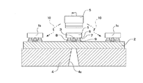
図5において、半導体素子1をフレキシブル基板2の上に実装する工程を説明する。3は仮止め用接着剤、4は搬送台、5は高温になる加熱加圧ツールである。
In the conventional flip chip technology, there is a mounting method using a temporary fixing adhesive as a method for preventing misalignment (see, for example, Patent Document 1).
In FIG. 5, a process of mounting the
最初に、半導体素子1のアクティブ面にあるアルミ電極6に突起電極7を形成し、突起電極7の上に導電性接着剤8を転写する。
次に、仮止め用接着剤3をディスペンス工法によりフレキシブル基板2上の半導体素子1を実装する部分に塗布する。
First, the protruding electrode 7 is formed on the
Next, the
次に、導電性接着剤8が転写された突起電極7がフレキシブル基板2の上の基板電極9に接触するように位置合わせしながら実装する。その時点で、仮止め用接着剤3と半導体素子1が接触する。
Next, mounting is performed while positioning so that the protruding electrode 7 to which the
次に、仮止め用接着剤3を加熱により硬化させる。このときに加熱する手段としては、フレキシブル基板2および半導体素子1を含め全体を加熱する場合や、搬送台4に設けた穴4aを利用して微細なヒーターやレーザーを用いてスポット加熱する場合がある。仮止め用接着剤3が硬化すると、フレキシブル基板2と半導体素子1の実装位置が固定され、位置ズレが発生しにくい。その後、必要に応じて接合信頼性を向上させるために半導体素子1とフレキシブル基板2との隙間に封止樹脂を流し込み、加熱により硬化させる。
しかしこの従来の方法では、仮止め用接着剤3を用いて半導体素子1とフレキシブル基板2とを仮止め固定する工程と、半導体素子1とフレキシブル基板2との隙間に封止樹脂を流し込み加熱により硬化させて接合信頼性を確保するために固定する工程とが、別工程であって工程数が増大している。
However, in this conventional method, the step of temporarily fixing and fixing the
また、半導体素子1の面積に対し、仮止め用接着剤3を塗布する面積が小さく、半導体素子1に水平方向の力を与えると、仮止め用接着剤3の弾性により仮止め位置がマイクロメーターのオーダーで移動する問題がある。
Further, when the area for applying the
また、1枚の回路基板に複数の半導体素子1を実装する場合において、高温になった加熱加圧ツール5からの輻射熱10のために隣接した半導体素子1b,1cの温度が高くなり、接合に用いる接着材の反応が進むため、接合不良になることがある。このため、隣接間距離を狭くすることができず、高密度実装ができない問題がある。
Further, when a plurality of
本発明は、半導体素子の仮止めの位置ズレがなく、しかも実装工程を少なくでき、かつ高密度実装ができる半導体素子の実装方法を提供することを目的とする。 SUMMARY OF THE INVENTION An object of the present invention is to provide a method for mounting a semiconductor element that does not cause misalignment of the temporary fixing of the semiconductor element, can reduce the mounting process, and can perform high-density mounting.
本発明の請求項1記載の半導体素子実装方法は、基板に仮止めされた半導体素子を高温の加熱加圧ツールで押圧して実装するに際し、仮止め中の前記半導体素子に接触して基板との平行度を矯正し、その後に前記加熱加圧ツールが仮止め中の前記半導体素子に近接して押圧して実装するとともに、仮止め中の半導体素子に接触して基板との平行度を矯正する工程は、半導体素子をテープにて押圧することを特徴とする。
本発明の請求項2記載の半導体素子実装方法は、基板に仮止めされた半導体素子を高温の加熱加圧ツールで押圧して実装するに際し、仮止め中の前記半導体素子に接触して基板との平行度を矯正し、その後に前記加熱加圧ツールが仮止め中の前記半導体素子に近接して押圧する工程では、前記半導体素子に隣接する実装部品との間に熱遮蔽部を介装して前記加熱加圧ツールから前記実装部品への熱伝導を遮蔽して実装するとともに、仮止め中の半導体素子に接触して基板との平行度を矯正する工程は、半導体素子をテープにて押圧することを特徴とする。
In the semiconductor element mounting method according to
In the semiconductor element mounting method according to
本発明の請求項3記載の半導体素子実装装置は、基板に仮止めされた半導体素子を高温の加熱加圧ツールで押圧して実装する半導体素子実装装置であって、仮止め中の前記半導体素子を押圧して基板との平行度を矯正する部品姿勢矯正手段と、前記加熱加圧ツールが仮止め中の前記半導体素子に近接して押圧する押圧手段とを設け、前記部品姿勢矯正手段は、架張されたテープにて前記半導体素子を押圧するよう構成したことを特徴とする。
本発明の請求項4記載の半導体素子実装装置は、基板に仮止めされた半導体素子を高温の加熱加圧ツールで押圧して実装する半導体素子実装装置であって、仮止め中の前記半導体素子を押圧して基板との平行度を矯正する部品姿勢矯正手段と、前記加熱加圧ツールが仮止め中の前記半導体素子に近接して押圧する状態で前記半導体素子に隣接する実装部品との間に熱遮蔽部を介装して熱伝導を遮蔽する熱遮蔽手段とを設け、前記部品姿勢矯正手段は、架張されたテープにて前記半導体素子を押圧するよう構成したことを特徴とする。
A semiconductor element mounting apparatus according to
A semiconductor element mounting apparatus according to
本発明の請求項5記載の半導体素子実装装置は、基板に仮止めされた半導体素子を高温の加熱加圧ツールで押圧して実装する半導体素子実装装置であって、仮止め中の前記半導体素子を押圧して基板との平行度を矯正する部品姿勢矯正手段と、前記加熱加圧ツールが仮止め中の前記半導体素子に近接して押圧する押圧手段と、前記加熱加圧ツールが仮止め中の前記半導体素子に近接して押圧する状態で前記半導体素子に隣接する実装部品との間に熱遮蔽部を介装して熱伝導を遮蔽する熱遮蔽手段とを設け、前記部品姿勢矯正手段と熱遮蔽手段が一体構造であり、仮止め中の半導体素子をテープにて押圧して基板との平行度を矯正するよう構成し、かつ前記テープを支持するテープ支持部を隣接する実装部品との間に介装して熱伝導を遮蔽する熱遮蔽部として構成したことを特徴とする。
本発明の請求項6記載の半導体素子実装装置は、請求項4において、前記部品姿勢矯正手段と熱遮蔽手段が一体構造であり、仮止め中の半導体素子をテープにて押圧して基板との平行度を矯正するよう構成し、かつ前記テープを押圧するテープ支持部を隣接する実装部品との間に介装して熱伝導を遮蔽する熱遮蔽部となるよう構成したことを特徴とする。
A semiconductor element mounting apparatus according to
According to a sixth aspect of the present invention, there is provided the semiconductor element mounting apparatus according to the fourth aspect , wherein the component posture correcting means and the heat shielding means are integrated, and the temporarily fixed semiconductor element is pressed with a tape to It is configured to correct parallelism, and is configured to be a heat shielding part that shields heat conduction by interposing a tape support part that presses the tape between adjacent mounting parts.
この構成によると、半導体素子と回路基板の電気的かつ機械的に接合する工程において位置ズレすることなく、高密度実装できる。 According to this arrangement, without misalignment in the step of electrically and mechanically bonding the semiconductor element and the circuit board, it high density mounting.
以下、本発明の半導体素子実装方法を具体的な実施の形態に基づいて説明する。
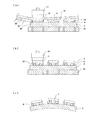
図1(a)(b)は本発明の半導体素子実装方法の実施に使用する半導体素子実装装置を示す。
Hereinafter, a semiconductor device mounting method of the present invention will be described based on specific embodiments.
FIGS. 1A and 1B show a semiconductor element mounting apparatus used for carrying out the semiconductor element mounting method of the present invention.
フレキシブル基板2が載置された搬送台4に対して、昇降が自在のホルダー11は、中央に加熱加圧ツール5が通過する連通孔12が形成されている。また、このホルダー11には、下降した状態でフレキシブル基板2を押さえる基板当接部13a,13bが設けられている。このホルダー11には、基板当接部13a,13bの先端に切り欠き14が形成されている。さらに、基板当接部13a,13bの間隔は、半導体素子1に応じてそれよりも幅広の間隔の所定間隔に配置されており、基板当接部13aの切り欠き14と基板当接部13bの切り欠き14を通過してテープ15が架張されている。詳しくは、テープ15の巻装体は軸16にセットされており、この巻装体から引き出されたテープ15が巻き取り軸17に巻き取られている。軸16と巻き取り軸17もホルダー11に取り付けられている。
A
なお、テープ15は12.5μm厚のポリイミドフィルムと5.0μm厚のフッ化樹脂フィルムの2層構造で、そのポリイミドフィルムの弾性率は550MPa、フッ化樹脂フィルムの弾性率は392MPaのものを使用している。
The
図2(a)(b)(c)は図1に示した実装装置にセットする前のフレキシブル基板2の作成工程を示しており、次のようにして半導体素子1が仮止めされている。
図2(a)では、フレキシブル基板2の上に、カットした樹脂シート18を貼り付ける。具体的には、樹脂シート供給用テープ19に貼られた樹脂シートにカット部20を入れた後に、加熱加圧ツール21を用いて半導体素子の実装領域のみに樹脂シート供給用テープ19の上から押圧する。この時の加熱加圧ツール21の温度は樹脂シート18が硬化反応を起こさず、かつ、樹脂シート18の軟化を起こさせフレキシブル基板2への貼り付けを容易にする温度が必要であり、通常60〜100℃、0.1〜1秒の押圧で貼り付けを行う。
FIGS. 2A, 2B, and 2C show a process of creating the
In FIG. 2A, the
次に図2(b)に示すように、フレキシブル基板2を作業台22に吸着させてフラットにした状態で、半導体素子1を実装ヘッド23で真空吸着してホールドし、基板電極9と半導体素子1に形成した突起電極7が接するように荷重1〜3kgf程度で±5μm以下の精度で半導体素子1を仮止めする。
Next, as shown in FIG. 2B, in a state where the
次に図2(c)では、作業台22の吸着をオフし、フレキシブル基板2を作業台22から取り外し、図1の搬送台4に乗せ換える。その時点でフレキシブル基板2は変形し、中央の半導体素子1のようにマウント状態が変化する場合がある。また、フレキシブル基板2のそれ自身の反りが原因でマウント状態が変化する場合がある。
Next, in FIG.2 (c), adsorption | suction of the
このようにマウント状態が変化した半導体素子1を有したフレキシブル基板2を図1の搬送台4に乗せ換えた直後の状態を図3(a)に示す。この際には、前記ホルダー11と加熱加圧ツール5は共に上昇位置にある。
FIG. 3A shows a state immediately after the
図3(b)では、ホルダー11と加熱加圧ツール5が一体に降下を始める。降下中のホルダー11の前記基板当接部13a,13bの間に所定のテンションで架張された前記テープ15が半導体素子1の背面に当接し、さらにホルダー11が降下することによって、前記マウント状態が変化した半導体素子1にテープ15から半導体素子1へ下向きの力が働き、半導体素子1の傾きが矯正される。なお、ここではテープ15の弾性が有効に作用して、ホルダー11の降下量が一定であっても、半導体素子1の各種の傾きを矯正できる。
In FIG. 3B, the
さらにホルダー11を降下させると、基板当接部13a,13bの先端が図4(a)のようにフレキシブル基板2に接触し、フレキシブル基板2に下方の力を加える。この力でフレキシブル基板2の反りを直し、搬送台4にフレキシブル基板2を密着させ、同時にフレキシブル基板2と半導体素子1を平行にする。
When the
次に、図4(b)に示すように、ホルダー11でフレキシブル基板2に下方の力を加えたまま、ホルダー11に対して加熱加圧ツール5を降下させて、テープ15を介して半導体素子1を押圧して加熱する。接合条件は30〜70kgfの加圧、180〜200℃の加熱を、10〜20秒間行う。なお、加熱加圧ツール5のテープ15との当接面にはダイヤモンドチップ5aが取り付けられている。
Next, as shown in FIG. 4B, the heating and
この圧着工程において、突起電極7は基板電極9上で変形しながら接触面積を増加させて電気的接続を得る。同時に樹脂シート18に加えた熱により、樹脂硬化反応を起こし、突起電極7と基板電極9が電気的に接続した状態を維持する。
In this crimping step, the protruding electrode 7 is deformed on the
さらにこの図4(b)から明らかなように、加熱加圧ツール5が半導体素子1を押圧している10〜20秒間の状態に注目すると、隣接する実装部品としての半導体素子1bと加熱加圧ツール5との間には、基板当接部13aの前記切り欠き部14よりも上部の熱遮蔽部としてのテープ支持部24aが介在して熱輻射を遮蔽している。また隣接する実装部品としての半導体素子1cと加熱加圧ツール5との間には、基板当接部13bの前記切り欠き部14よりも上部の熱遮蔽部としてのテープ支持部24bが介在して熱輻射を遮蔽している。このように加熱加圧ツール5から半導体素子1b,1cへの熱輻射を遮ることによって、高密度実装の場合であっても正常な実装状態が得られる。また搬送台4からの熱伝導を抑えるために、本実施例では、搬送台4を1つの半導体素子サイズよりも僅かに大きな小型化したものを使用し、2つの効果により、半導体素子1b,1cの樹脂シート18の熱硬化反応が発生せず、良好な接合を得ている。具体的には、熱遮蔽部24a,24bを設けなかった場合には、図4(b)の工程を実施した場合には、半導体素子1b,1cの温度が80〜100℃に上昇したが、テープ支持部24a,24bを設けることによって40〜60℃に抑制された。
Further, as apparent from FIG. 4B, when attention is paid to the state of 10 to 20 seconds in which the heating and
樹脂シート18の硬化により半導体素子1とフレキシブル基板3とが電気的に接続され、かつ機械的に固定された状態になると、図4(c)に示すように加熱加圧ツール5を上昇させ、加熱と加圧を終了させる。その後にホルダー11を上昇させて1つの半導体素子の実装を終了する。
When the
なお、単数または複数の半導体素子の実装が完了するたびに、巻き取り軸17に巻き取られて更新されている。
なお、上記の実施の形態において、仮止め中の前記半導体素子1を押圧してフレキシブル基板2との平行度を矯正する部品姿勢矯正手段は、ホルダー11に架張されたテープ15によって構成されている。また、加熱加圧ツール5が仮止め中の前記半導体素子1に近接して押圧する状態で前記半導体素子1に隣接する実装部品との間に熱遮蔽部を介装して熱伝導を遮蔽する熱遮蔽手段は、ホルダー11に設けられてテープ15を支持しているテープ支持部24a,24bによって構成されている。
なお、上記の実施の形態では基板の具体例がフレキシブル基板2の場合を例に挙げて説明したが、弾性を有する多層基板の場合にも同様に実施できる。
Each time the mounting of one or a plurality of semiconductor elements is completed, it is wound around the winding
In the above embodiment, the component posture correcting means for correcting the parallelism with the
In the above embodiment, the case where the specific example of the substrate is the
本発明は、例えば、薄く反り易い樹脂で出来たフレキシブル基板に、複数の半導体素子をフリップチップ実装工法を実施する際に、基板の反りと半導体素子の傾きを矯正し、かつ隣接半導体素子の輻射熱による温度上昇を抑え、位置ズレが無く、良好な接合品質を得ることができ、小型軽量化が要求される携帯電話装置やデジタルカメラなどの製品に使用される半導体パッケージの良好な実装を期待できる。 The present invention, for example, corrects the warpage of the semiconductor element and the inclination of the semiconductor element when performing the flip chip mounting method on a flexible substrate made of a thin and easily warped resin, and radiant heat of the adjacent semiconductor element. The temperature rise due to the above can be suppressed, there is no positional deviation, good bonding quality can be obtained, and good mounting of semiconductor packages used in products such as mobile phone devices and digital cameras that require miniaturization and weight reduction can be expected .
1 半導体素子
2 フレキシブル基板
4 搬送台
5 加熱加圧ツール
5a ダイヤモンドチップ
7 突起電極
9 基板電極
11 ホルダー
12 連通孔
13a,13b 基板当接部
14 切り欠き
15 テープ
16 軸
17 巻き取り軸
18 樹脂シート
19 樹脂シート供給用テープ
20 カット部
21 加熱加圧ツール
22 作業台
23 実装ヘッド
24a,24b テープ支持部(熱遮蔽部)
DESCRIPTION OF
Claims (6)
仮止め中の前記半導体素子に接触して基板との平行度を矯正し、
その後に前記加熱加圧ツールが仮止め中の前記半導体素子に近接して押圧して実装するとともに、仮止め中の半導体素子に接触して基板との平行度を矯正する工程は、半導体素子をテープにて押圧する
半導体素子実装方法。 When mounting the semiconductor element temporarily fixed to the substrate with a high-temperature heating and pressing tool,
Correct the parallelism with the substrate in contact with the semiconductor element being temporarily fixed,
Thereafter, the heating and pressing tool presses and mounts close to the semiconductor element being temporarily fixed, and the step of contacting the semiconductor element being temporarily fixed and correcting the parallelism with the substrate includes the steps of: Method of mounting semiconductor device by pressing with tape .
仮止め中の前記半導体素子に接触して基板との平行度を矯正し、
その後に前記加熱加圧ツールが仮止め中の前記半導体素子に近接して押圧する工程では、前記半導体素子に隣接する実装部品との間に熱遮蔽部を介装して前記加熱加圧ツールから前記実装部品への熱伝導を遮蔽して実装する
とともに、仮止め中の半導体素子に接触して基板との平行度を矯正する工程は、半導体素子をテープにて押圧する
半導体素子実装方法。 When mounting the semiconductor element temporarily fixed to the substrate with a high-temperature heating and pressing tool,
Correct the parallelism with the substrate in contact with the semiconductor element being temporarily fixed,
Thereafter, in the step of pressing the heating and pressing tool close to the semiconductor element being temporarily fixed, a heat shielding part is interposed between the mounting component adjacent to the semiconductor element and the heating and pressing tool from the heating and pressing tool. Mounted by shielding heat conduction to the mounting parts
At the same time, the step of correcting the parallelism with the substrate by contacting the temporarily fixed semiconductor element presses the semiconductor element with a tape .
仮止め中の前記半導体素子を押圧して基板との平行度を矯正する部品姿勢矯正手段と、
前記加熱加圧ツールが仮止め中の前記半導体素子に近接して押圧する押圧手段と
を設け、
前記部品姿勢矯正手段は、架張されたテープにて前記半導体素子を押圧するよう構成し
た半導体素子実装装置。 A semiconductor element mounting apparatus for mounting a semiconductor element temporarily fixed to a substrate by pressing with a high temperature heating and pressing tool,
Component posture correcting means for correcting the parallelism with the substrate by pressing the semiconductor element being temporarily fixed;
A pressing means for pressing the heating and pressing tool in proximity to the semiconductor element being temporarily fixed ;
The semiconductor element mounting apparatus, wherein the component posture correcting means is configured to press the semiconductor element with a stretched tape .
仮止め中の前記半導体素子を押圧して基板との平行度を矯正する部品姿勢矯正手段と、
前記加熱加圧ツールが仮止め中の前記半導体素子に近接して押圧する押圧手段と、
前記加熱加圧ツールが仮止め中の前記半導体素子に近接して押圧する状態で前記半導体素子に隣接する実装部品との間に熱遮蔽部を介装して熱伝導を遮蔽する熱遮蔽手段と
を設け、
前記部品姿勢矯正手段は、架張されたテープにて前記半導体素子を押圧するよう構成した半導体素子実装装置。 A semiconductor element mounting apparatus for mounting a semiconductor element temporarily fixed to a substrate by pressing with a high temperature heating and pressing tool,
Component posture correcting means for correcting the parallelism with the substrate by pressing the semiconductor element being temporarily fixed;
A pressing means for pressing the heating and pressing tool close to the semiconductor element being temporarily fixed;
A heat shielding means for shielding heat conduction by interposing a heat shielding part between the heating and pressing tool and a mounting component adjacent to the semiconductor element in a state of pressing in proximity to the semiconductor element being temporarily fixed; Provided ,
The component orientation correcting means is a semiconductor element mounting apparatus configured to press the semiconductor element with a stretched tape .
仮止め中の前記半導体素子を押圧して基板との平行度を矯正する部品姿勢矯正手段と、
前記加熱加圧ツールが仮止め中の前記半導体素子に近接して押圧する押圧手段と、
前記加熱加圧ツールが仮止め中の前記半導体素子に近接して押圧する状態で前記半導体素子に隣接する実装部品との間に熱遮蔽部を介装して熱伝導を遮蔽する熱遮蔽手段と
を設け、
前記部品姿勢矯正手段と熱遮蔽手段が一体構造であり、仮止め中の半導体素子をテープにて押圧して基板との平行度を矯正するよう構成し、かつ前記テープを支持するテープ支持部を隣接する実装部品との間に介装して熱伝導を遮蔽する熱遮蔽部として構成した
半導体素子実装装置。 A semiconductor element mounting apparatus for mounting a semiconductor element temporarily fixed to a substrate by pressing with a high temperature heating and pressing tool,
Component posture correcting means for correcting the parallelism with the substrate by pressing the semiconductor element being temporarily fixed;
A pressing means for pressing the heating and pressing tool close to the semiconductor element being temporarily fixed;
A heat shielding means for shielding heat conduction by interposing a heat shielding part between the heating and pressing tool and a mounting component adjacent to the semiconductor element in a state of pressing in proximity to the semiconductor element being temporarily fixed; Provided ,
The component posture correcting means and the heat shielding means are integrally structured, and are configured to correct the parallelism with the substrate by pressing the semiconductor element being temporarily fixed with a tape, and a tape support portion for supporting the tape. A semiconductor element mounting apparatus configured as a heat shielding portion that is interposed between adjacent mounting components and shields heat conduction .
仮止め中の半導体素子をテープにて押圧して基板との平行度を矯正するよう構成し、かつ前記テープを支持するテープ支持部を隣接する実装部品との間に介装して熱伝導を遮蔽する熱遮蔽部として構成した
請求項4に記載の半導体素子実装装置。 The component posture correcting means and the heat shielding means have an integral structure,
The semiconductor element being temporarily fixed is pressed with a tape so as to correct the parallelism with the substrate, and a tape support part for supporting the tape is interposed between adjacent mounting parts for heat conduction. Configured as a heat shield to shield
The semiconductor element mounting apparatus according to claim 4 .
Priority Applications (1)
| Application Number | Priority Date | Filing Date | Title |
|---|---|---|---|
| JP2005187498A JP4619209B2 (en) | 2005-06-28 | 2005-06-28 | Semiconductor element mounting method and semiconductor element mounting apparatus |
Applications Claiming Priority (1)
| Application Number | Priority Date | Filing Date | Title |
|---|---|---|---|
| JP2005187498A JP4619209B2 (en) | 2005-06-28 | 2005-06-28 | Semiconductor element mounting method and semiconductor element mounting apparatus |
Publications (3)
| Publication Number | Publication Date |
|---|---|
| JP2007012641A JP2007012641A (en) | 2007-01-18 |
| JP2007012641A5 JP2007012641A5 (en) | 2008-04-17 |
| JP4619209B2 true JP4619209B2 (en) | 2011-01-26 |
Family
ID=37750798
Family Applications (1)
| Application Number | Title | Priority Date | Filing Date |
|---|---|---|---|
| JP2005187498A Expired - Fee Related JP4619209B2 (en) | 2005-06-28 | 2005-06-28 | Semiconductor element mounting method and semiconductor element mounting apparatus |
Country Status (1)
| Country | Link |
|---|---|
| JP (1) | JP4619209B2 (en) |
Families Citing this family (5)
| Publication number | Priority date | Publication date | Assignee | Title |
|---|---|---|---|---|
| JP5122192B2 (en) * | 2007-07-04 | 2013-01-16 | パナソニック株式会社 | Semiconductor device mounting equipment |
| JP5024117B2 (en) * | 2007-10-09 | 2012-09-12 | 日立化成工業株式会社 | Circuit member mounting method |
| US9362196B2 (en) * | 2010-07-15 | 2016-06-07 | Kabushiki Kaisha Toshiba | Semiconductor package and mobile device using the same |
| KR102191179B1 (en) * | 2019-02-07 | 2020-12-15 | (주)에이피텍 | Pulse heater power dispensing solution with alignment plate curing heater |
| WO2022013995A1 (en) * | 2020-07-16 | 2022-01-20 | 株式会社新川 | Mounting device |
Citations (7)
| Publication number | Priority date | Publication date | Assignee | Title |
|---|---|---|---|---|
| JPH02122531A (en) * | 1988-11-01 | 1990-05-10 | Matsushita Electric Ind Co Ltd | Device for mounting electronic component |
| JPH05144881A (en) * | 1991-11-18 | 1993-06-11 | Matsushita Electric Ind Co Ltd | Manufacture of mounting device and semiconductor device |
| JPH09107008A (en) * | 1995-10-12 | 1997-04-22 | Oki Electric Ind Co Ltd | Mounting method and device of semiconductor element |
| JP2000277569A (en) * | 1999-03-25 | 2000-10-06 | Toshiba Corp | Device and method for leveling and bonding |
| JP2001068847A (en) * | 1999-08-25 | 2001-03-16 | Fujitsu Ltd | Method and device for mounting electronic component |
| JP2002305214A (en) * | 2001-04-05 | 2002-10-18 | Toray Eng Co Ltd | Chip-bonding method and its device |
| JP2003152028A (en) * | 2001-11-12 | 2003-05-23 | Matsushita Electric Ind Co Ltd | Method and apparatus for mounting electronic parts |
-
2005
- 2005-06-28 JP JP2005187498A patent/JP4619209B2/en not_active Expired - Fee Related
Patent Citations (7)
| Publication number | Priority date | Publication date | Assignee | Title |
|---|---|---|---|---|
| JPH02122531A (en) * | 1988-11-01 | 1990-05-10 | Matsushita Electric Ind Co Ltd | Device for mounting electronic component |
| JPH05144881A (en) * | 1991-11-18 | 1993-06-11 | Matsushita Electric Ind Co Ltd | Manufacture of mounting device and semiconductor device |
| JPH09107008A (en) * | 1995-10-12 | 1997-04-22 | Oki Electric Ind Co Ltd | Mounting method and device of semiconductor element |
| JP2000277569A (en) * | 1999-03-25 | 2000-10-06 | Toshiba Corp | Device and method for leveling and bonding |
| JP2001068847A (en) * | 1999-08-25 | 2001-03-16 | Fujitsu Ltd | Method and device for mounting electronic component |
| JP2002305214A (en) * | 2001-04-05 | 2002-10-18 | Toray Eng Co Ltd | Chip-bonding method and its device |
| JP2003152028A (en) * | 2001-11-12 | 2003-05-23 | Matsushita Electric Ind Co Ltd | Method and apparatus for mounting electronic parts |
Also Published As
| Publication number | Publication date |
|---|---|
| JP2007012641A (en) | 2007-01-18 |
Similar Documents
| Publication | Publication Date | Title |
|---|---|---|
| US8163599B2 (en) | Flip-chip mounting method, flip-chip mounting apparatus and tool protection sheet used in flip-chip mounting apparatus | |
| JP4139713B2 (en) | Reinforcing plate pasting device and pasting method | |
| JPWO2010050209A1 (en) | Method and apparatus for joining electronic component and flexible film substrate | |
| JP6029245B2 (en) | Crimping apparatus and crimping method | |
| JP4619209B2 (en) | Semiconductor element mounting method and semiconductor element mounting apparatus | |
| JP3896017B2 (en) | Semiconductor mounting body manufacturing method and semiconductor mounting body manufacturing apparatus | |
| JP5122192B2 (en) | Semiconductor device mounting equipment | |
| WO2019054284A1 (en) | Compression head and mounting device | |
| KR100950523B1 (en) | Printed circuit board assembly and electronic device | |
| TWI392422B (en) | Method of manufacturing wiring board mounting electric components | |
| US20110126409A1 (en) | Method of manufacturing printed circuit board | |
| KR20210052774A (en) | System for flip chip bonding and method for flip chip bonding using the same | |
| US7743491B2 (en) | Mounting method of passive component | |
| JP2013012513A (en) | Mounting method of electronic component | |
| JP2004327944A (en) | Mounting method of wiring board | |
| JP3997838B2 (en) | Driver IC crimping apparatus and crimping method | |
| JP2002141373A (en) | Method and apparatus for mounting semiconductor | |
| JP5288898B2 (en) | Adhesive sheet sticking device and sticking method, and electronic component mounting device and mounting method | |
| JP4228839B2 (en) | Bonding equipment | |
| JP2011187699A (en) | Semiconductor device and method of manufacturing the same | |
| JP4052144B2 (en) | Manufacturing method of semiconductor device | |
| JP2001189553A (en) | Bonding device for substrate and method for bonding substrate using the same | |
| JP2006179811A (en) | Method of packaging semiconductor device and its packaging device | |
| JP6461822B2 (en) | Semiconductor device mounting method and mounting apparatus | |
| JP2006253179A (en) | Method and apparatus of manufacturing semiconductor device |
Legal Events
| Date | Code | Title | Description |
|---|---|---|---|
| A521 | Written amendment |
Free format text: JAPANESE INTERMEDIATE CODE: A523 Effective date: 20080303 |
|
| A621 | Written request for application examination |
Free format text: JAPANESE INTERMEDIATE CODE: A621 Effective date: 20080303 |
|
| RD04 | Notification of resignation of power of attorney |
Free format text: JAPANESE INTERMEDIATE CODE: A7424 Effective date: 20080430 |
|
| A977 | Report on retrieval |
Free format text: JAPANESE INTERMEDIATE CODE: A971007 Effective date: 20100712 |
|
| A131 | Notification of reasons for refusal |
Free format text: JAPANESE INTERMEDIATE CODE: A131 Effective date: 20100720 |
|
| A521 | Written amendment |
Free format text: JAPANESE INTERMEDIATE CODE: A523 Effective date: 20100908 |
|
| TRDD | Decision of grant or rejection written | ||
| A01 | Written decision to grant a patent or to grant a registration (utility model) |
Free format text: JAPANESE INTERMEDIATE CODE: A01 Effective date: 20100928 |
|
| A01 | Written decision to grant a patent or to grant a registration (utility model) |
Free format text: JAPANESE INTERMEDIATE CODE: A01 |
|
| A61 | First payment of annual fees (during grant procedure) |
Free format text: JAPANESE INTERMEDIATE CODE: A61 Effective date: 20101026 |
|
| FPAY | Renewal fee payment (event date is renewal date of database) |
Free format text: PAYMENT UNTIL: 20131105 Year of fee payment: 3 |
|
| FPAY | Renewal fee payment (event date is renewal date of database) |
Free format text: PAYMENT UNTIL: 20131105 Year of fee payment: 3 |
|
| LAPS | Cancellation because of no payment of annual fees |