JP6926012B2 - Semiconductor device - Google Patents
Semiconductor device Download PDFInfo
- Publication number
- JP6926012B2 JP6926012B2 JP2018024047A JP2018024047A JP6926012B2 JP 6926012 B2 JP6926012 B2 JP 6926012B2 JP 2018024047 A JP2018024047 A JP 2018024047A JP 2018024047 A JP2018024047 A JP 2018024047A JP 6926012 B2 JP6926012 B2 JP 6926012B2
- Authority
- JP
- Japan
- Prior art keywords
- conductive
- region
- electrode
- semiconductor
- conductive portion
- Prior art date
- Legal status (The legal status is an assumption and is not a legal conclusion. Google has not performed a legal analysis and makes no representation as to the accuracy of the status listed.)
- Active
Links
- 239000004065 semiconductor Substances 0.000 title claims description 216
- 230000003071 parasitic effect Effects 0.000 description 13
- 239000012535 impurity Substances 0.000 description 11
- 238000000034 method Methods 0.000 description 10
- 229920002120 photoresistant polymer Polymers 0.000 description 9
- 238000009413 insulation Methods 0.000 description 6
- 238000004519 manufacturing process Methods 0.000 description 6
- 239000000758 substrate Substances 0.000 description 6
- 238000011084 recovery Methods 0.000 description 5
- 239000000969 carrier Substances 0.000 description 4
- 229910052751 metal Inorganic materials 0.000 description 4
- 239000002184 metal Substances 0.000 description 4
- 230000015556 catabolic process Effects 0.000 description 3
- 239000000463 material Substances 0.000 description 3
- 230000004048 modification Effects 0.000 description 3
- 238000012986 modification Methods 0.000 description 3
- 238000001020 plasma etching Methods 0.000 description 3
- 229910052785 arsenic Inorganic materials 0.000 description 2
- RQNWIZPPADIBDY-UHFFFAOYSA-N arsenic atom Chemical compound [As] RQNWIZPPADIBDY-UHFFFAOYSA-N 0.000 description 2
- 238000005229 chemical vapour deposition Methods 0.000 description 2
- 238000010586 diagram Methods 0.000 description 2
- 230000002093 peripheral effect Effects 0.000 description 2
- 238000001004 secondary ion mass spectrometry Methods 0.000 description 2
- 229910052710 silicon Inorganic materials 0.000 description 2
- 239000010703 silicon Substances 0.000 description 2
- 238000004544 sputter deposition Methods 0.000 description 2
- ZOXJGFHDIHLPTG-UHFFFAOYSA-N Boron Chemical compound [B] ZOXJGFHDIHLPTG-UHFFFAOYSA-N 0.000 description 1
- 229910002601 GaN Inorganic materials 0.000 description 1
- GYHNNYVSQQEPJS-UHFFFAOYSA-N Gallium Chemical compound [Ga] GYHNNYVSQQEPJS-UHFFFAOYSA-N 0.000 description 1
- JMASRVWKEDWRBT-UHFFFAOYSA-N Gallium nitride Chemical compound [Ga]#N JMASRVWKEDWRBT-UHFFFAOYSA-N 0.000 description 1
- OAICVXFJPJFONN-UHFFFAOYSA-N Phosphorus Chemical compound [P] OAICVXFJPJFONN-UHFFFAOYSA-N 0.000 description 1
- VYPSYNLAJGMNEJ-UHFFFAOYSA-N Silicium dioxide Chemical compound O=[Si]=O VYPSYNLAJGMNEJ-UHFFFAOYSA-N 0.000 description 1
- XUIMIQQOPSSXEZ-UHFFFAOYSA-N Silicon Chemical compound [Si] XUIMIQQOPSSXEZ-UHFFFAOYSA-N 0.000 description 1
- 229910052782 aluminium Inorganic materials 0.000 description 1
- XAGFODPZIPBFFR-UHFFFAOYSA-N aluminium Chemical compound [Al] XAGFODPZIPBFFR-UHFFFAOYSA-N 0.000 description 1
- 229910052787 antimony Inorganic materials 0.000 description 1
- WATWJIUSRGPENY-UHFFFAOYSA-N antimony atom Chemical compound [Sb] WATWJIUSRGPENY-UHFFFAOYSA-N 0.000 description 1
- 229910052796 boron Inorganic materials 0.000 description 1
- 239000004020 conductor Substances 0.000 description 1
- 230000006866 deterioration Effects 0.000 description 1
- 238000001312 dry etching Methods 0.000 description 1
- 230000000694 effects Effects 0.000 description 1
- 230000005669 field effect Effects 0.000 description 1
- 229910052733 gallium Inorganic materials 0.000 description 1
- 230000005484 gravity Effects 0.000 description 1
- 239000011810 insulating material Substances 0.000 description 1
- 238000005468 ion implantation Methods 0.000 description 1
- 150000002500 ions Chemical class 0.000 description 1
- 239000007769 metal material Substances 0.000 description 1
- 229910044991 metal oxide Inorganic materials 0.000 description 1
- 150000004706 metal oxides Chemical class 0.000 description 1
- 238000000059 patterning Methods 0.000 description 1
- 229910052698 phosphorus Inorganic materials 0.000 description 1
- 239000011574 phosphorus Substances 0.000 description 1
- 238000000206 photolithography Methods 0.000 description 1
- 229910021420 polycrystalline silicon Inorganic materials 0.000 description 1
- 229920005591 polysilicon Polymers 0.000 description 1
- 229910010271 silicon carbide Inorganic materials 0.000 description 1
- HBMJWWWQQXIZIP-UHFFFAOYSA-N silicon carbide Chemical compound [Si+]#[C-] HBMJWWWQQXIZIP-UHFFFAOYSA-N 0.000 description 1
- 229910052814 silicon oxide Inorganic materials 0.000 description 1
- 239000000126 substance Substances 0.000 description 1
- 238000001039 wet etching Methods 0.000 description 1
Images


Classifications
-
- H—ELECTRICITY
- H01—ELECTRIC ELEMENTS
- H01L—SEMICONDUCTOR DEVICES NOT COVERED BY CLASS H10
- H01L29/00—Semiconductor devices adapted for rectifying, amplifying, oscillating or switching, or capacitors or resistors with at least one potential-jump barrier or surface barrier, e.g. PN junction depletion layer or carrier concentration layer; Details of semiconductor bodies or of electrodes thereof ; Multistep manufacturing processes therefor
- H01L29/66—Types of semiconductor device ; Multistep manufacturing processes therefor
- H01L29/68—Types of semiconductor device ; Multistep manufacturing processes therefor controllable by only the electric current supplied, or only the electric potential applied, to an electrode which does not carry the current to be rectified, amplified or switched
- H01L29/76—Unipolar devices, e.g. field effect transistors
- H01L29/772—Field effect transistors
- H01L29/78—Field effect transistors with field effect produced by an insulated gate
- H01L29/7801—DMOS transistors, i.e. MISFETs with a channel accommodating body or base region adjoining a drain drift region
- H01L29/7802—Vertical DMOS transistors, i.e. VDMOS transistors
- H01L29/7813—Vertical DMOS transistors, i.e. VDMOS transistors with trench gate electrode, e.g. UMOS transistors
-
- H—ELECTRICITY
- H01—ELECTRIC ELEMENTS
- H01L—SEMICONDUCTOR DEVICES NOT COVERED BY CLASS H10
- H01L29/00—Semiconductor devices adapted for rectifying, amplifying, oscillating or switching, or capacitors or resistors with at least one potential-jump barrier or surface barrier, e.g. PN junction depletion layer or carrier concentration layer; Details of semiconductor bodies or of electrodes thereof ; Multistep manufacturing processes therefor
- H01L29/02—Semiconductor bodies ; Multistep manufacturing processes therefor
- H01L29/06—Semiconductor bodies ; Multistep manufacturing processes therefor characterised by their shape; characterised by the shapes, relative sizes, or dispositions of the semiconductor regions ; characterised by the concentration or distribution of impurities within semiconductor regions
- H01L29/0603—Semiconductor bodies ; Multistep manufacturing processes therefor characterised by their shape; characterised by the shapes, relative sizes, or dispositions of the semiconductor regions ; characterised by the concentration or distribution of impurities within semiconductor regions characterised by particular constructional design considerations, e.g. for preventing surface leakage, for controlling electric field concentration or for internal isolations regions
- H01L29/0607—Semiconductor bodies ; Multistep manufacturing processes therefor characterised by their shape; characterised by the shapes, relative sizes, or dispositions of the semiconductor regions ; characterised by the concentration or distribution of impurities within semiconductor regions characterised by particular constructional design considerations, e.g. for preventing surface leakage, for controlling electric field concentration or for internal isolations regions for preventing surface leakage or controlling electric field concentration
- H01L29/0611—Semiconductor bodies ; Multistep manufacturing processes therefor characterised by their shape; characterised by the shapes, relative sizes, or dispositions of the semiconductor regions ; characterised by the concentration or distribution of impurities within semiconductor regions characterised by particular constructional design considerations, e.g. for preventing surface leakage, for controlling electric field concentration or for internal isolations regions for preventing surface leakage or controlling electric field concentration for increasing or controlling the breakdown voltage of reverse biased devices
- H01L29/0615—Semiconductor bodies ; Multistep manufacturing processes therefor characterised by their shape; characterised by the shapes, relative sizes, or dispositions of the semiconductor regions ; characterised by the concentration or distribution of impurities within semiconductor regions characterised by particular constructional design considerations, e.g. for preventing surface leakage, for controlling electric field concentration or for internal isolations regions for preventing surface leakage or controlling electric field concentration for increasing or controlling the breakdown voltage of reverse biased devices by the doping profile or the shape or the arrangement of the PN junction, or with supplementary regions, e.g. junction termination extension [JTE]
-
- H—ELECTRICITY
- H01—ELECTRIC ELEMENTS
- H01L—SEMICONDUCTOR DEVICES NOT COVERED BY CLASS H10
- H01L29/00—Semiconductor devices adapted for rectifying, amplifying, oscillating or switching, or capacitors or resistors with at least one potential-jump barrier or surface barrier, e.g. PN junction depletion layer or carrier concentration layer; Details of semiconductor bodies or of electrodes thereof ; Multistep manufacturing processes therefor
- H01L29/02—Semiconductor bodies ; Multistep manufacturing processes therefor
- H01L29/06—Semiconductor bodies ; Multistep manufacturing processes therefor characterised by their shape; characterised by the shapes, relative sizes, or dispositions of the semiconductor regions ; characterised by the concentration or distribution of impurities within semiconductor regions
- H01L29/0684—Semiconductor bodies ; Multistep manufacturing processes therefor characterised by their shape; characterised by the shapes, relative sizes, or dispositions of the semiconductor regions ; characterised by the concentration or distribution of impurities within semiconductor regions characterised by the shape, relative sizes or dispositions of the semiconductor regions or junctions between the regions
- H01L29/0692—Surface layout
- H01L29/0696—Surface layout of cellular field-effect devices, e.g. multicellular DMOS transistors or IGBTs
-
- H—ELECTRICITY
- H01—ELECTRIC ELEMENTS
- H01L—SEMICONDUCTOR DEVICES NOT COVERED BY CLASS H10
- H01L29/00—Semiconductor devices adapted for rectifying, amplifying, oscillating or switching, or capacitors or resistors with at least one potential-jump barrier or surface barrier, e.g. PN junction depletion layer or carrier concentration layer; Details of semiconductor bodies or of electrodes thereof ; Multistep manufacturing processes therefor
- H01L29/02—Semiconductor bodies ; Multistep manufacturing processes therefor
- H01L29/06—Semiconductor bodies ; Multistep manufacturing processes therefor characterised by their shape; characterised by the shapes, relative sizes, or dispositions of the semiconductor regions ; characterised by the concentration or distribution of impurities within semiconductor regions
- H01L29/10—Semiconductor bodies ; Multistep manufacturing processes therefor characterised by their shape; characterised by the shapes, relative sizes, or dispositions of the semiconductor regions ; characterised by the concentration or distribution of impurities within semiconductor regions with semiconductor regions connected to an electrode not carrying current to be rectified, amplified or switched and such electrode being part of a semiconductor device which comprises three or more electrodes
- H01L29/1095—Body region, i.e. base region, of DMOS transistors or IGBTs
-
- H—ELECTRICITY
- H01—ELECTRIC ELEMENTS
- H01L—SEMICONDUCTOR DEVICES NOT COVERED BY CLASS H10
- H01L29/00—Semiconductor devices adapted for rectifying, amplifying, oscillating or switching, or capacitors or resistors with at least one potential-jump barrier or surface barrier, e.g. PN junction depletion layer or carrier concentration layer; Details of semiconductor bodies or of electrodes thereof ; Multistep manufacturing processes therefor
- H01L29/40—Electrodes ; Multistep manufacturing processes therefor
- H01L29/402—Field plates
- H01L29/407—Recessed field plates, e.g. trench field plates, buried field plates
-
- H—ELECTRICITY
- H01—ELECTRIC ELEMENTS
- H01L—SEMICONDUCTOR DEVICES NOT COVERED BY CLASS H10
- H01L29/00—Semiconductor devices adapted for rectifying, amplifying, oscillating or switching, or capacitors or resistors with at least one potential-jump barrier or surface barrier, e.g. PN junction depletion layer or carrier concentration layer; Details of semiconductor bodies or of electrodes thereof ; Multistep manufacturing processes therefor
- H01L29/40—Electrodes ; Multistep manufacturing processes therefor
- H01L29/41—Electrodes ; Multistep manufacturing processes therefor characterised by their shape, relative sizes or dispositions
- H01L29/417—Electrodes ; Multistep manufacturing processes therefor characterised by their shape, relative sizes or dispositions carrying the current to be rectified, amplified or switched
- H01L29/41725—Source or drain electrodes for field effect devices
- H01L29/41766—Source or drain electrodes for field effect devices with at least part of the source or drain electrode having contact below the semiconductor surface, e.g. the source or drain electrode formed at least partially in a groove or with inclusions of conductor inside the semiconductor
-
- H—ELECTRICITY
- H01—ELECTRIC ELEMENTS
- H01L—SEMICONDUCTOR DEVICES NOT COVERED BY CLASS H10
- H01L29/00—Semiconductor devices adapted for rectifying, amplifying, oscillating or switching, or capacitors or resistors with at least one potential-jump barrier or surface barrier, e.g. PN junction depletion layer or carrier concentration layer; Details of semiconductor bodies or of electrodes thereof ; Multistep manufacturing processes therefor
- H01L29/40—Electrodes ; Multistep manufacturing processes therefor
- H01L29/41—Electrodes ; Multistep manufacturing processes therefor characterised by their shape, relative sizes or dispositions
- H01L29/423—Electrodes ; Multistep manufacturing processes therefor characterised by their shape, relative sizes or dispositions not carrying the current to be rectified, amplified or switched
- H01L29/42312—Gate electrodes for field effect devices
- H01L29/42316—Gate electrodes for field effect devices for field-effect transistors
- H01L29/4232—Gate electrodes for field effect devices for field-effect transistors with insulated gate
- H01L29/42356—Disposition, e.g. buried gate electrode
- H01L29/4236—Disposition, e.g. buried gate electrode within a trench, e.g. trench gate electrode, groove gate electrode
-
- H—ELECTRICITY
- H01—ELECTRIC ELEMENTS
- H01L—SEMICONDUCTOR DEVICES NOT COVERED BY CLASS H10
- H01L29/00—Semiconductor devices adapted for rectifying, amplifying, oscillating or switching, or capacitors or resistors with at least one potential-jump barrier or surface barrier, e.g. PN junction depletion layer or carrier concentration layer; Details of semiconductor bodies or of electrodes thereof ; Multistep manufacturing processes therefor
- H01L29/40—Electrodes ; Multistep manufacturing processes therefor
- H01L29/41—Electrodes ; Multistep manufacturing processes therefor characterised by their shape, relative sizes or dispositions
- H01L29/423—Electrodes ; Multistep manufacturing processes therefor characterised by their shape, relative sizes or dispositions not carrying the current to be rectified, amplified or switched
- H01L29/42312—Gate electrodes for field effect devices
- H01L29/42316—Gate electrodes for field effect devices for field-effect transistors
- H01L29/4232—Gate electrodes for field effect devices for field-effect transistors with insulated gate
- H01L29/42372—Gate electrodes for field effect devices for field-effect transistors with insulated gate characterised by the conducting layer, e.g. the length, the sectional shape or the lay-out
- H01L29/42376—Gate electrodes for field effect devices for field-effect transistors with insulated gate characterised by the conducting layer, e.g. the length, the sectional shape or the lay-out characterised by the length or the sectional shape
-
- H—ELECTRICITY
- H01—ELECTRIC ELEMENTS
- H01L—SEMICONDUCTOR DEVICES NOT COVERED BY CLASS H10
- H01L29/00—Semiconductor devices adapted for rectifying, amplifying, oscillating or switching, or capacitors or resistors with at least one potential-jump barrier or surface barrier, e.g. PN junction depletion layer or carrier concentration layer; Details of semiconductor bodies or of electrodes thereof ; Multistep manufacturing processes therefor
- H01L29/66—Types of semiconductor device ; Multistep manufacturing processes therefor
- H01L29/66007—Multistep manufacturing processes
- H01L29/66075—Multistep manufacturing processes of devices having semiconductor bodies comprising group 14 or group 13/15 materials
- H01L29/66227—Multistep manufacturing processes of devices having semiconductor bodies comprising group 14 or group 13/15 materials the devices being controllable only by the electric current supplied or the electric potential applied, to an electrode which does not carry the current to be rectified, amplified or switched, e.g. three-terminal devices
- H01L29/66409—Unipolar field-effect transistors
- H01L29/66477—Unipolar field-effect transistors with an insulated gate, i.e. MISFET
- H01L29/66674—DMOS transistors, i.e. MISFETs with a channel accommodating body or base region adjoining a drain drift region
- H01L29/66712—Vertical DMOS transistors, i.e. VDMOS transistors
- H01L29/66727—Vertical DMOS transistors, i.e. VDMOS transistors with a step of recessing the source electrode
-
- H—ELECTRICITY
- H01—ELECTRIC ELEMENTS
- H01L—SEMICONDUCTOR DEVICES NOT COVERED BY CLASS H10
- H01L29/00—Semiconductor devices adapted for rectifying, amplifying, oscillating or switching, or capacitors or resistors with at least one potential-jump barrier or surface barrier, e.g. PN junction depletion layer or carrier concentration layer; Details of semiconductor bodies or of electrodes thereof ; Multistep manufacturing processes therefor
- H01L29/66—Types of semiconductor device ; Multistep manufacturing processes therefor
- H01L29/66007—Multistep manufacturing processes
- H01L29/66075—Multistep manufacturing processes of devices having semiconductor bodies comprising group 14 or group 13/15 materials
- H01L29/66227—Multistep manufacturing processes of devices having semiconductor bodies comprising group 14 or group 13/15 materials the devices being controllable only by the electric current supplied or the electric potential applied, to an electrode which does not carry the current to be rectified, amplified or switched, e.g. three-terminal devices
- H01L29/66409—Unipolar field-effect transistors
- H01L29/66477—Unipolar field-effect transistors with an insulated gate, i.e. MISFET
- H01L29/66674—DMOS transistors, i.e. MISFETs with a channel accommodating body or base region adjoining a drain drift region
- H01L29/66712—Vertical DMOS transistors, i.e. VDMOS transistors
- H01L29/66734—Vertical DMOS transistors, i.e. VDMOS transistors with a step of recessing the gate electrode, e.g. to form a trench gate electrode
-
- H—ELECTRICITY
- H01—ELECTRIC ELEMENTS
- H01L—SEMICONDUCTOR DEVICES NOT COVERED BY CLASS H10
- H01L29/00—Semiconductor devices adapted for rectifying, amplifying, oscillating or switching, or capacitors or resistors with at least one potential-jump barrier or surface barrier, e.g. PN junction depletion layer or carrier concentration layer; Details of semiconductor bodies or of electrodes thereof ; Multistep manufacturing processes therefor
- H01L29/66—Types of semiconductor device ; Multistep manufacturing processes therefor
- H01L29/68—Types of semiconductor device ; Multistep manufacturing processes therefor controllable by only the electric current supplied, or only the electric potential applied, to an electrode which does not carry the current to be rectified, amplified or switched
- H01L29/76—Unipolar devices, e.g. field effect transistors
- H01L29/772—Field effect transistors
- H01L29/78—Field effect transistors with field effect produced by an insulated gate
- H01L29/7801—DMOS transistors, i.e. MISFETs with a channel accommodating body or base region adjoining a drain drift region
- H01L29/7802—Vertical DMOS transistors, i.e. VDMOS transistors
- H01L29/7803—Vertical DMOS transistors, i.e. VDMOS transistors structurally associated with at least one other device
- H01L29/7804—Vertical DMOS transistors, i.e. VDMOS transistors structurally associated with at least one other device the other device being a pn-junction diode
- H01L29/7805—Vertical DMOS transistors, i.e. VDMOS transistors structurally associated with at least one other device the other device being a pn-junction diode in antiparallel, e.g. freewheel diode
-
- H—ELECTRICITY
- H01—ELECTRIC ELEMENTS
- H01L—SEMICONDUCTOR DEVICES NOT COVERED BY CLASS H10
- H01L29/00—Semiconductor devices adapted for rectifying, amplifying, oscillating or switching, or capacitors or resistors with at least one potential-jump barrier or surface barrier, e.g. PN junction depletion layer or carrier concentration layer; Details of semiconductor bodies or of electrodes thereof ; Multistep manufacturing processes therefor
- H01L29/66—Types of semiconductor device ; Multistep manufacturing processes therefor
- H01L29/68—Types of semiconductor device ; Multistep manufacturing processes therefor controllable by only the electric current supplied, or only the electric potential applied, to an electrode which does not carry the current to be rectified, amplified or switched
- H01L29/76—Unipolar devices, e.g. field effect transistors
- H01L29/772—Field effect transistors
- H01L29/78—Field effect transistors with field effect produced by an insulated gate
- H01L29/7801—DMOS transistors, i.e. MISFETs with a channel accommodating body or base region adjoining a drain drift region
- H01L29/7802—Vertical DMOS transistors, i.e. VDMOS transistors
- H01L29/7811—Vertical DMOS transistors, i.e. VDMOS transistors with an edge termination structure
Description
本発明の実施形態は、半導体装置に関する。 Embodiments of the present invention relate to semiconductor devices.
MOSFET(Metal Oxide Semiconductor Field Effect Transistor)などの半導体装置は、スイッチング装置として用いられる。MOSFETは、寄生バイポーラトランジスタを含む。この寄生トランジスタが動作すると、半導体装置が破壊される可能性がある。このため、寄生トランジスタは動作し難いことが望ましい。 Semiconductor devices such as MOSFETs (Metal Oxide Semiconductor Field Effect Transistors) are used as switching devices. MOSFETs include parasitic bipolar transistors. When this parasitic transistor operates, the semiconductor device may be destroyed. Therefore, it is desirable that the parasitic transistor is difficult to operate.
本発明が解決しようとする課題は、寄生トランジスタの動作を抑制できる半導体装置を提供することである。 An object to be solved by the present invention is to provide a semiconductor device capable of suppressing the operation of a parasitic transistor.
実施形態に係る半導体装置は、第1電極と、第1導電形の第1半導体領域と、第2導電形の第2半導体領域と、第1導電形の第3半導体領域と、第2電極と、ゲート電極と、第1導電部と、第2導電部と、を備える。前記第1半導体領域は、前記第1電極の上に設けられている。前記第1半導体領域は、第1領域と、前記第1領域を囲む第2領域と、を有する。前記第2半導体領域は、前記第1領域の上に設けられている。前記第3半導体領域は、前記第2半導体領域の上に設けられている。前記第2電極は、前記第3半導体領域の上に設けられ、前記第2半導体領域及び前記第3半導体領域と電気的に接続されている。前記ゲート電極は、前記第1領域から前記第2半導体領域に向かう第1方向に垂直な第2方向において、前記第2半導体領域とゲート絶縁部を介して対向している。前記第1導電部は、前記第2領域の上の前記第1半導体領域中に第1絶縁部を介して設けられている。前記第1導電部は、前記第1方向及び前記第2方向に垂直な第3方向において、互いに離間して複数設けられている。複数の前記第1導電部は、前記第2方向において前記ゲート電極と並び、前記第2電極又は前記ゲート電極と電気的に接続されている。前記複数の第1導電部のうち隣り合う前記第1導電部の間には、前記第1半導体領域のみが設けられている。前記第2導電部は、前記第2電極又は前記ゲート電極と電気的に接続されている。前記第2導電部は、前記第2領域の上の前記第1半導体領域中に第2絶縁部を介して設けられている。前記第2導電部は、前記第3方向において前記ゲート電極及び前記複数の第1導電部と並んでいる。前記第2導電部と、前記複数の第1導電部のうち前記第2導電部と隣り合う前記第1導電部と、の間には、前記第1半導体領域のみが設けられている。前記第1導電部の前記第2方向における長さは、前記ゲート電極の前記第2方向における長さよりも長い。
The semiconductor device according to the embodiment includes a first electrode, a first conductive type first semiconductor region, a second conductive type second semiconductor region, a first conductive type third semiconductor region, and a second electrode. , A gate electrode, a first conductive portion, and a second conductive portion. The first semiconductor region is provided on the first electrode. The first semiconductor region has a first region and a second region surrounding the first region. The second semiconductor region is provided above the first region. The third semiconductor region is provided above the second semiconductor region. The second electrode is provided on the third semiconductor region and is electrically connected to the second semiconductor region and the third semiconductor region. The gate electrode faces the second semiconductor region via a gate insulating portion in a second direction perpendicular to the first direction from the first region to the second semiconductor region. The first conductive portion is provided in the first semiconductor region above the second region via a first insulating portion. A plurality of the first conductive portions are provided so as to be separated from each other in the first direction and the third direction perpendicular to the second direction. The plurality of first conductive portions are aligned with the gate electrode in the second direction and are electrically connected to the second electrode or the gate electrode. Only the first semiconductor region is provided between the adjacent first conductive portions among the plurality of first conductive portions. The second conductive portion is electrically connected to the second electrode or the gate electrode. The second conductive portion is provided in the first semiconductor region above the second region via a second insulating portion. The second conductive portion is aligned with the gate electrode and the plurality of first conductive portions in the third direction. Only the first semiconductor region is provided between the second conductive portion and the first conductive portion adjacent to the second conductive portion among the plurality of first conductive portions. The length of the first conductive portion in the second direction is longer than the length of the gate electrode in the second direction.
以下に、本発明の各実施形態について図面を参照しつつ説明する。
なお、図面は模式的または概念的なものであり、各部分の厚みと幅との関係、部分間の大きさの比率などは、必ずしも現実のものと同一とは限らない。また、同じ部分を表す場合であっても、図面により互いの寸法や比率が異なって表される場合もある。
また、本願明細書と各図において、既に説明したものと同様の要素には同一の符号を付して詳細な説明は適宜省略する。
以下の説明及び図面において、n+、n−及びp+、pの表記は、各導電形における不純物濃度の相対的な高低を表す。すなわち、「+」が付されている表記は、「+」及び「−」のいずれも付されていない表記よりも不純物濃度が相対的に高く、「−」が付されている表記は、いずれも付されていない表記よりも不純物濃度が相対的に低いことを示す。
以下で説明する各実施形態について、各半導体領域のp形とn形を反転させて各実施形態を実施してもよい。
Hereinafter, each embodiment of the present invention will be described with reference to the drawings.
The drawings are schematic or conceptual, and the relationship between the thickness and width of each part, the ratio of the sizes between the parts, and the like are not necessarily the same as the actual ones. Further, even when the same parts are represented, the dimensions and ratios may be different from each other depending on the drawings.
Further, in the present specification and each figure, the same elements as those already described are designated by the same reference numerals, and detailed description thereof will be omitted as appropriate.
In the following description and drawings, the notations n + , n − and p + , p represent the relative high and low concentrations of impurities in each conductive form. That is, the notation with "+" has a relatively higher impurity concentration than the notation without either "+" or "-", and the notation with "-" is any of them. Indicates that the impurity concentration is relatively lower than the notation not marked with.
For each of the embodiments described below, the p-type and the n-type of each semiconductor region may be inverted to carry out each embodiment.
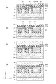
(第1実施形態)
図1は、第1実施形態に係る半導体装置を表す平面図である。
図2は、図1のA−A’断面図である。
図3は、図1のB−B’断面図及びC−C’断面図である。
なお、図1は、図2のD−D’線の位置で切断した面を表し、図1では、各半導体領域が省略されている。
(First Embodiment)
FIG. 1 is a plan view showing a semiconductor device according to the first embodiment.
FIG. 2 is a cross-sectional view taken along the line AA'of FIG.
FIG. 3 is a cross-sectional view taken along the line BB and a cross-sectional view taken along the line CC of FIG.
Note that FIG. 1 shows a surface cut at the position of the DD'line in FIG. 2, and each semiconductor region is omitted in FIG.
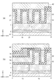
半導体装置100は、例えばMOSFETである。半導体装置100は、図1〜図3に表したように、n−形(第1導電形)半導体領域1(第1半導体領域)、p形(第2導電形)ベース領域2(第2半導体領域)、n+形ソース領域3(第3半導体領域)、p+形コンタクト領域4(第4半導体領域)、n+形ドレイン領域5(第5半導体領域)、フィールドプレート電極(以下FP電極という)10、ゲート電極14、第1導電部21、第2導電部22、ドレイン電極41(第1電極)、ソース電極42(第2電極)、及びゲートパッド43(第3電極)を有する。
The
実施形態の説明では、XYZ直交座標系を用いる。n−形半導体領域1の第1領域1aからp形ベース領域2に向かう方向をZ方向(第1方向)とする。Z方向に対して垂直であり、相互に直交する2方向をX方向(第2方向)及びY方向(第3方向)とする。また、説明のために、第1領域1aからp形ベース領域2に向かう方向を「上」と言い、その反対方向を「下」と言う。これらの方向は、第1領域1aとp形ベース領域2との位置関係に基づき、重力の方向とは無関係である。
In the description of the embodiment, the XYZ Cartesian coordinate system is used. the n - direction from the
図1では、ソース電極42及びゲートパッド43が、破線で表されている。図1に表したように、ソース電極42及びゲートパッド43は、半導体装置100の上面に設けられ、互いに離間している。ソース電極42の下には、FP電極10、ゲート電極14、第1導電部21、及び第2導電部22が設けられている。
In FIG. 1, the
図2に表したように、ドレイン電極41は、半導体装置100の下面に設けられている。n+形ドレイン領域5は、ドレイン電極41の上に設けられ、ドレイン電極41と電気的に接続されている。n−形半導体領域1は、n+形ドレイン領域5の上に設けられている。n−形半導体領域1は、第1領域1aと、第1領域1aを囲む第2領域1bと、を有する。第1領域1aから第2領域1bに向かう方向は、Z方向に垂直である。p形ベース領域2は、第1領域1aの上に設けられている。n+形ソース領域3及びp+形コンタクト領域4は、p形ベース領域2の上に設けられている。
As shown in FIG. 2, the
FP電極10は、第1領域1aの上に、絶縁部11を介して設けられている。ゲート電極14は、FP電極10の上に絶縁部12を介して設けられている。また、ゲート電極14は、X方向において、n−形半導体領域1の一部、p形ベース領域2、及びn+形ソース領域3の少なくとも一部とゲート絶縁部15を介して対向している。ゲート電極14の上には、絶縁部35が設けられている。ゲート電極14は、ゲートパッド43と電気的に接続されている。
The
ソース電極42の一部は、絶縁部35中に設けられ、n+形ソース領域3及びp+形コンタクト領域4と電気的に接続されている。図2に表した例では、p+形コンタクト領域4がn+形ソース領域3よりも下方に位置し、n+形ソース領域3はX方向においてソース電極42の一部と並んでいる。ソース電極42の電位は、例えばグランドに設定される。ゲート電極14とソース電極42は、絶縁部35によって電気的に分離されている。FP電極10は、ソース電極42またはゲート電極14(ゲートパッド43)と電気的に接続されている。
A part of the
p形ベース領域2、n+形ソース領域3、p+形コンタクト領域4、FP電極10、及びゲート電極14のそれぞれは、第1領域1aの上において、X方向に複数設けられ、Y方向に延びている。
A plurality of p-
第1導電部21は、図1に表したように、Y方向において複数設けられている。複数の第1導電部21は、互いに離間している。複数の第1導電部21は、X方向においてゲート電極14と並んでいる。図1の例では、第1導電部21は、さらに、X方向において複数設けられている。複数のゲート電極14は、X方向において、複数の第1導電部21の一部と、複数の第1導電部21の別の一部と、の間に位置している。
As shown in FIG. 1, a plurality of first
第2導電部22は、X方向に延びている。第2導電部22は、Y方向において、複数のゲート電極14及び複数の第1導電部21と並んでいる。図1の例では、第2導電部22は、Y方向において複数設けられている。複数のゲート電極14及び複数の第1導電部21は、Y方向において、第2導電部22と、別の第2導電部22と、の間に位置している。
The second
複数の第1導電部21及び複数の第2導電部22は、例えば、ゲートパッド43の下に位置しないように、ソース電極42の下にのみ設けられている。
The plurality of first
図2に表したように、第1導電部21は、第2領域1bの上に、第1絶縁部31を介して設けられている。第1導電部21は、X方向及びY方向において、n−形半導体領域1の一部と第1絶縁部31を介して対向している。第1導電部21は、例えば、ソース電極42と電気的に接続されている。または、第1導電部21は、ゲート電極14及びゲートパッド43と電気的に接続されていても良い。
As shown in FIG. 2, the first
第1導電部21とp形ベース領域2との間の第1絶縁部31中には、例えば、第4導電部24が設けられている。第4導電部24は、X方向において第1導電部21と離間している。例えば、第4導電部24のX方向における長さは、第1導電部21のX方向における長さより短い。第4導電部24のZ方向における長さは、第1導電部21のZ方向における長さより短い。第4導電部24の電位は、例えば、フローティングである。または、第4導電部24は、ソース電極42と電気的に接続されていても良い。
For example, a fourth
図3(a)及び図3(b)に表したように、第2導電部22は、第2領域1bの上に、第2絶縁部32を介して設けられている。第2導電部22は、X方向及びY方向において、n−形半導体領域1の一部と第2絶縁部32を介して対向している。第2導電部22は、例えば、ソース電極42と電気的に接続されている。または、第2導電部22は、ゲート電極14及びゲートパッド43と電気的に接続されていても良い。
As shown in FIGS. 3A and 3B, the second
例えば、図3(a)及び図3(b)に表したように、第1導電部21と第2導電部22は、連続してつながっている。第1絶縁部31と第2絶縁部32は、連続してつながっている。
For example, as shown in FIGS. 3A and 3B, the first
半導体装置100の各構成要素の材料の一例を説明する。
n−形半導体領域1、p形ベース領域2、n+形ソース領域3、p+形コンタクト領域4、及びn+形ドレイン領域5は、半導体材料として、シリコン、炭化シリコン、窒化ガリウム、またはガリウムヒ素を含む。半導体材料としてシリコンが用いられる場合、n形不純物として、ヒ素、リン、またはアンチモンを用いることができる。p形不純物として、ボロンを用いることができる。
FP電極10、ゲート電極14、第1導電部21、及び第2導電部22は、ポリシリコンなどの導電材料を含む。
絶縁部11、絶縁部12、ゲート絶縁部15、第1絶縁部31、及び第2絶縁部32は、酸化シリコンなどの絶縁材料を含む。
ドレイン電極41、ソース電極42、及びゲートパッド43は、アルミニウムなどの金属を含む。
An example of the material of each component of the
the n -
The
The insulating
The
半導体装置100の動作を説明する。
ソース電極42に対してドレイン電極41に正の電圧が印加された状態で、ゲート電極14に閾値以上の電圧が印加されると、p形ベース領域2のゲート絶縁部15近傍にチャネル(反転層)が形成され、半導体装置100がオン状態となる。電子は、このチャネルを通ってソース電極42からドレイン電極41へ流れる。その後、ゲート電極14に印加される電圧が閾値よりも低くなると、p形ベース領域2におけるチャネルが消滅し、半導体装置100がオフ状態になる。
The operation of the
When a positive voltage is applied to the
半導体装置100の製造方法の一例を説明する。
図4〜図6は、第1実施形態に係る半導体装置の製造工程を表す工程断面図である。
図4〜図6は、図1のA−A’断面に対応する部分の製造工程を表している。
An example of a method for manufacturing the
4 to 6 are process cross-sectional views showing a manufacturing process of the semiconductor device according to the first embodiment.
4 to 6 show the manufacturing process of the portion corresponding to the AA'cross section of FIG.
まず、n+形半導体領域5mと、n+形半導体領域5mの上に設けられたn−形半導体領域1mと、を有する半導体基板Sを用意する。n−形半導体領域1mの上面に、フォトリソグラフィ法及びRIE(Reactive Ion Etching)法を用いて、図4(a)に表したように、トレンチT1及びT2を形成する。トレンチT1は、X方向において複数形成され、それぞれがY方向に延びている。トレンチT2は、Y方向において複数形成される。トレンチT2のX方向における寸法は、トレンチT1のX方向における寸法よりも長い。トレンチT1は、FP電極10及びゲート電極14を形成するためのトレンチである。トレンチT2は、第1導電部21を形成するためのトレンチである。その他に、この工程において、第2導電部22を形成するための不図示のトレンチが形成される。
First, a semiconductor substrate S having an n + type
半導体基板Sを熱酸化し、n−形半導体領域1mの表面に沿って絶縁層11mを形成する。図4(b)に表したように、絶縁層11mの上に、CVD(Chemical Vapor Deposition)法を用いて、トレンチT1及びT2を埋め込む導電層10mを形成する。
The semiconductor substrate S is thermally oxidized, n - along the surface of the
図4(c)に表したように、導電層10mの一部を除去することで、互いに分離された複数の導電層10nを形成する。トレンチT2内に形成された導電層10nを不図示のマスクで覆い、図4(d)に表したように、トレンチT1内に形成された導電層10nの一部を除去する。トレンチT1内に残った導電層10nは、FP電極10に対応する。トレンチT2内に残った導電層10nは、第1導電部21に対応する。
As shown in FIG. 4C, by removing a part of the
トレンチT2を含む半導体基板Sの外周を不図示のマスクで覆い、図5(a)に表したように、ウェットエッチングにより絶縁層11mの一部を除去する。これにより、トレンチT1の内面の一部及びトレンチT2の内面の一部が露出する。半導体基板Sを熱酸化し、トレンチT1の内面、トレンチT2の内面、及び第1導電部21の表面に、絶縁層11mよりも薄い絶縁部15mを形成する。FP電極10の上面には、絶縁層12mが形成される。
The outer circumference of the semiconductor substrate S including the trench T2 is covered with a mask (not shown), and as shown in FIG. 5A, a part of the insulating
図5(b)に表したように、絶縁部15mの上に、トレンチT1及びT2を埋め込む導電層14mを形成する。CDE(Chemical Dry Etching)法またはRIE法を用いて導電層14mの一部を除去することで、図5(c)に表したように、トレンチT1内及びトレンチT2内にそれぞれ設けられた、複数の導電層を形成する。トレンチT1内に形成された導電層は、ゲート電極14に対応する。トレンチT2内に形成された導電層は、第4導電部24に対応する。
As shown in FIG. 5B, a
トレンチT1同士の間及びトレンチT1とT2との間にp形不純物をイオン注入し、p形半導体領域2mを形成する。トレンチT1同士の間のp形半導体領域2mの表面に、n形不純物をイオン注入し、n+形半導体領域3mを形成する。図5(d)に表したように、ゲート電極14及び第4導電部24を覆う絶縁層35mを形成する。
Ion implantation of p-type impurities between the trenches T1 and between the trenches T1 and T2 forms a p-
絶縁層35mの上に、フォトレジストPRを形成する。図6(a)に表したように、フォトレジストPRに複数の開口OP1及び開口OP2を形成する。絶縁層35mの一部が、複数の開口OP1及び開口OP2を通して露出する。複数の開口OP1は、それぞれ、複数のp形半導体領域2mの直上に位置する。開口OP2は、第1導電部21の直上に位置する。
A photoresist PR is formed on the insulating
フォトレジストPRをマスクとして用いて、複数の開口OP3及び開口OP4を形成する。それぞれの開口OP3は、絶縁層35m、絶縁部15m、及びn+形半導体領域3mを貫通し、p形半導体領域2mに達する。開口OP4は、絶縁層35m及び絶縁部15mを貫通している。フォトレジストPRを除去し、開口OP3の底部にp形不純物をイオン注入する。これにより、図6(b)に表したように、p+形コンタクト領域4が形成される。p+形コンタクト領域4以外のp形半導体領域2mは、p形ベース領域2に対応する。n+形半導体領域3mは、n+形ソース領域3に対応する。
Using the photoresist PR as a mask, a plurality of openings OP3 and OP4 are formed. Each opening OP3 penetrates the insulating
図6(c)に表したように、絶縁層35mの上に、スパッタリング法を用いて金属層を形成する。複数の開口OP3及び開口OP4は、この金属層により埋め込まれる。この金属層をパターニングすることで、ソース電極42及びゲートパッド43を形成する。n+形半導体領域5mの下面を、n+形半導体領域5mが所定の厚みになるまで研削する。図6(d)に表したように、研削したn+形半導体領域5mの下面に、スパッタリング法を用いて金属材料を堆積させ、ドレイン電極41を形成する。以上の工程により、図1〜図3に表した半導体装置100が製造される。
As shown in FIG. 6C, a metal layer is formed on the insulating
図4(a)に表した工程で形成されるトレンチT1及びT2について、トレンチT2のX方向における寸法は、トレンチT1のX方向における寸法よりも長い。これにより、図6(a)に表したように、絶縁層11mの上面及び第1導電部21の上面の間の段差st1と、第1導電部21と、のX方向における距離を長くできる。これに伴い、絶縁層35mの上面に形成される段差st2と、第1導電部21と、のX方向における距離も長くなる。この結果、フォトレジストPRの表面において段差st3が生じる位置を、開口OP2が形成される位置よりも、半導体基板Sの外周側にずらすことができる。
Regarding the trenches T1 and T2 formed in the process shown in FIG. 4A, the dimension of the trench T2 in the X direction is longer than the dimension of the trench T1 in the X direction. As a result, as shown in FIG. 6A, the distance between the step st1 between the upper surface of the insulating
フォトレジストPRの段差st3が存在する部分の厚みは、ゲート電極14上などのフォトレジストPRの他の部分の厚みよりも大きい。このため、段差st3の位置と開口OP2の位置が重なると、開口OP2を形成する際に、フォトレジストPRが十分に除去されず、絶縁層35mが露出しない可能性がある。開口OP2を通して絶縁層35mが露出していない場合、開口OP4が適切に形成されない。この結果、第1導電部21がソース電極42と接続されない可能性がある。上述したように、段差st3の位置を、開口OP2が形成される位置からずらすことで、開口OP4を適切に形成することが可能となる。
The thickness of the portion of the photoresist PR where the step st3 exists is larger than the thickness of other portions of the photoresist PR, such as on the
第1実施形態の効果を、図7〜図9を参照して説明する。
図7は、第1実施形態に係る半導体装置が接続された電気回路を例示する回路図である。
図8は、図7に表した電気回路中の半導体装置における電流および電圧の波形を表すグラフである。
図9は、第1実施形態に係る半導体装置中の正孔の流れを模式的に表す平面図である。
なお、図9では、n−形半導体領域1及びp形ベース領域2以外の半導体領域が省略されている。
The effects of the first embodiment will be described with reference to FIGS. 7 to 9.
FIG. 7 is a circuit diagram illustrating an electric circuit to which the semiconductor device according to the first embodiment is connected.
FIG. 8 is a graph showing current and voltage waveforms in the semiconductor device in the electric circuit shown in FIG. 7.
FIG. 9 is a plan view schematically showing the flow of holes in the semiconductor device according to the first embodiment.
In FIG. 9, n -
図7(a)〜図7(c)に表す例では、本実施形態に係る2つの半導体装置100−1と100−2が用いられ、ハーフブリッジ回路が構成されている。図7(a)は、半導体装置100−1がオン状態、半導体装置100−2がオフ状態のときの様子を表している。半導体装置100−1には、オン電流IONが流れている。 In the examples shown in FIGS. 7 (a) to 7 (c), the two semiconductor devices 100-1 and 100-2 according to the present embodiment are used to form a half-bridge circuit. FIG. 7A shows a state when the semiconductor device 100-1 is in the on state and the semiconductor device 100-2 is in the off state. An on-current ION is flowing through the semiconductor device 100-1.
図7(a)に表した状態で、半導体装置100−1がターンオフされると、インダクタンスLによる誘導起電力が生じる。これにより、図7(b)に表したように、半導体装置100−2のn−形半導体領域1とp形ベース領域2から構成されるダイオードに、順方向の電流IFが流れる。このとき、ソース電極42からn−形半導体領域1へ正孔が注入され、ドレイン電極41からn−形半導体領域1へ電子が注入される。
When the semiconductor device 100-1 is turned off in the state shown in FIG. 7A, an induced electromotive force due to the inductance L is generated. Thus, as shown in FIG. 7 (b), n of the semiconductor device 100-2 - the formed diodes from
半導体装置100−2のダイオードに順方向電流が流れきると、半導体装置100−2の内部に蓄積されたキャリアが排出される。このとき、n−形半導体領域1に蓄積された正孔はソース電極42へ排出され、電子はドレイン電極41へ排出される。半導体装置100−2からキャリアが排出されることで、図7(c)に表すように、半導体装置100−2には、ドレイン電極41からソース電極42に向かって逆回復電流IRが流れる。
When the forward current flows through the diode of the semiconductor device 100-2, the carriers accumulated inside the semiconductor device 100-2 are discharged. At this time, n - holes accumulated in
図8において、実線は、半導体装置100−2を流れる電流を表し、破線は、ソース電極42に対するドレイン電極41の電圧を表している。横軸は時間を表し、縦軸は電流値を表している。電流値は、ドレイン電極41からソース電極42に向かう方向を正として表している。
In FIG. 8, the solid line represents the current flowing through the semiconductor device 100-2, and the broken line represents the voltage of the
図8に表したように、タイミングt1で順方向電流が流れきると、その後、逆回復電流が流れ始めるとともに、半導体装置100−2のソース電極42に対するドレイン電極41の電圧Vが上昇していく。このとき、逆回復電流の減少の傾きdIR/dtに応じて、電圧Vにサージ電圧Vsが発生する。dIR/dtが大きいと、サージ電圧Vsも大きくなる。サージ電圧Vsが大きいと、n+形ソース領域3、p形ベース領域2、およびn−形半導体領域1から構成される寄生NPNトランジスタが動作し易くなる。寄生NPNトランジスタが動作すると、半導体装置内を大電流が流れ、半導体装置が破壊される可能性がある。このため、dIR/dtは、小さいことが望ましい。
As shown in FIG. 8, when the forward current flows completely at the timing t1, the reverse recovery current starts to flow and the voltage V of the
ダイオード動作時に注入されたキャリアの一部は、n−形半導体領域1の外周にも蓄積される。n−形半導体領域1の外周に蓄積された正孔は、逆回復動作時には、近くのp形ベース領域2に移動してソース電極42へ排出される。従って、外周側に設けられたp形ベース領域2には、他の部分に比べて多くの正孔が流れる。このため、p形ベース領域2の電位が上昇し易く、より寄生NPNトランジスタが動作し易い。
Some of the carriers injected during the diode operation, n - is also accumulated on the outer periphery of the
この課題について、半導体装置100では、n−形半導体領域1の第2領域1bの上に、互いに離間した複数の第1導電部21が設けられている。複数の第1導電部21は、ソース電極42またはゲート電極14(ゲートパッド43)と電気的に接続されている。すなわち、半導体装置100がオフ状態のとき、第1導電部21の電位は、正孔に対して負である。
この構成によれば、n−形半導体領域1の外周に蓄積された正孔hの一部は、図9の点線矢印で表したように、第1導電部21同士の間を通過してp形ベース領域2へ流れる。正孔hの別の一部は、破線矢印で表したように、第1絶縁部31近傍でトラップされる。トラップされた正孔hは、トラップされなかった正孔hに比べて、長い時間をかけてp形ベース領域2へ流れる。
このように、互いに離間した複数の第1導電部21が設けられることで、正孔hがp形ベース領域2に達するまでの時間のばらつきを大きくできる。この結果、図8に表したdIR/dtを小さくでき、寄生NPNトランジスタの動作により半導体装置が破壊される可能性を低減できる。
For this problem, in the
According to this configuration, n - the part of the holes h accumulated on the outer periphery of the
By providing the plurality of first
図9に表したように、第1導電部21のX方向における長さL1は、ゲート電極14のX方向における長さL2よりも長いことが望ましい。長さL1が長いことで、正孔hがよりトラップされ易くなり、dIR/dtをさらに小さくできる。
As shown in FIG. 9, it is desirable that the length L1 of the first
第1絶縁部31同士の間のY方向における距離D1は、ゲート絶縁部15同士の間のX方向における距離D2と同じか、それよりも短いことが望ましい。距離D1は、例えば、n−形半導体領域1の第1絶縁部31同士の間の部分の、Y方向における長さと同じである。距離D2は、例えば、n−形半導体領域1のゲート絶縁部15同士の間の部分の、X方向における長さと同じである。距離D2は、例えば、ゲート絶縁部15同士の間のp形ベース領域2のX方向における長さと同じである。
It is desirable that the distance D1 between the first insulating
例えば、第1絶縁部31の厚みは、ゲート絶縁部15の厚みよりも大きい。この場合、半導体装置100をターンオフした際に、第1絶縁部31近傍のn−形半導体領域1では、ゲート電極14及びFP電極10近傍のn−形半導体領域1よりも空乏層が広がり難くなる。複数の第1導電部21が互いに離間した構成において、距離D1が長いと、第1絶縁部31同士の間のn−形半導体領域1が空乏化し難くなり、半導体装置100の耐圧が低下する可能性がある。
第1絶縁部31同士の間のn−形半導体領域1を空乏化させ易くし、半導体装置100の耐圧の低下を抑制するためには、距離D1が距離D2以下であることが望ましい。より望ましくは、距離D1は、距離D2未満である。これにより、第1絶縁部31同士の間のn−形半導体領域1がより空乏化し易くなり、半導体装置100の耐圧の低下を抑制できる。
For example, the thickness of the first insulating
N between each other the first insulating portion 31 - a
第1絶縁部31と第2絶縁部32との間のY方向における距離D3は、距離D2と同じか、それよりも短いことが望ましい。距離D3は、例えば、n−形半導体領域1の第1絶縁部31と第2絶縁部32との間の部分の、Y方向における長さと同じである。この構成によれば、上記と同様に、半導体装置100の耐圧の低下を抑制できる。
It is desirable that the distance D3 in the Y direction between the first insulating
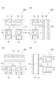
(変形例)
図10は、第1実施形態の変形例に係る半導体装置を表す平面図である。
図11は、図10のA−A’断面図である。
なお、図10の平面図は、図11のB−B’線における断面を表している。
(Modification example)
FIG. 10 is a plan view showing a semiconductor device according to a modified example of the first embodiment.
FIG. 11 is a cross-sectional view taken along the line AA'of FIG.
The plan view of FIG. 10 shows a cross section taken along the line BB'of FIG.
第1実施形態の変形例に係る半導体装置110は、図10に表したように、複数の第3導電部23をさらに備える。複数の第3導電部23は、Y方向において互いに離間している。それぞれの第3導電部23は、X方向に延びている。また、それぞれの第3導電部23の一部は、ゲートパッド43の下に位置している。
As shown in FIG. 10, the
ゲート電極14の一部は、X方向において、複数の第1導電部21と、複数の第3導電部23と、の間に位置している。第2導電部22の一部は、ゲートパッド43の下に設けられている。複数の第3導電部23は、Y方向において、第1導電部21と第2導電部22の一部との間及び複数のゲート電極14と第2導電部22の別の一部との間に位置している。第3導電部23のX方向における長さは、ゲート電極14及び第1導電部21のそれぞれのX方向における長さよりも長い。
A part of the
図11に表したように、第3導電部23は、第2領域1bの上に第3絶縁部33を介して設けられている。第3導電部23は、X方向及びY方向において、n−形半導体領域1の一部と第3絶縁部33を介して対向している。ゲートパッド43は、第3導電部23の上に、絶縁部36を介して設けられている。第3導電部23は、ソース電極42と電気的に接続されている。または、第3導電部23は、ゲート電極14及びゲートパッド43と電気的に接続されていても良い。
As shown in FIG. 11, the third conductive portion 23 is provided on the
半導体装置100のダイオードに電流が流れると、ゲートパッド43の下のn−形半導体領域1にもキャリアが蓄積される。ゲートパッド43の下に蓄積された正孔は、ゲートパッド43に近いp形ベース領域2へ流れる。このため、ゲートパッド43に近いp形ベース領域2では、電位が上昇し易く、より寄生NPNトランジスタが動作し易い。
When a current flows through the diode of the
図10に表したように、複数の第3導電部23が設けられることで、複数の第1導電部21と同様に、正孔hがソース電極42へ排出される際、正孔hの一部をトラップできる。これにより、ゲートパッド43付近における寄生NPNトランジスタの動作を抑制でき、半導体装置が破壊される可能性をさらに低減できる。
As shown in FIG. 10, by providing the plurality of third conductive portions 23, as in the case of the plurality of first
(第2実施形態)
図12は、第2実施形態に係る半導体装置を表す平面図である。
図13は、図12のA−A’断面図及びB−B’断面図である。
図14は、図12のC−C’断面図である。
なお、図12の平面図は、図13のD−D’線における断面を表している。
(Second Embodiment)
FIG. 12 is a plan view showing the semiconductor device according to the second embodiment.
13 is a cross-sectional view taken along the line AA and a cross-sectional view taken along the line BB of FIG.
Figure 14 is a C-C 'sectional view of FIG. 12.
The plan view of FIG. 12 shows a cross section taken along the line DD'of FIG.
第2実施形態に係る半導体装置200では、図12に表したように、複数の第1導電部21が、X方向において互いに離間している。複数の第1導電部21は、Y方向において複数のゲート電極14と並んでいる。第2導電部22は、X方向において、ゲート電極14及び第1導電部21と並んでいる。
In the
図12に表した例では、複数のゲート電極14は、Y方向において、複数の第1導電部21の一部と、複数の第1導電部21の別の一部と、の間に位置している。また、それぞれのゲート電極14の少なくとも一部は、X方向において、第2導電部22と、別の第2導電部22と、の間に位置している。
In the example shown in FIG. 12, the plurality of
図13(a)に表したように、例えば、ゲート絶縁部15と第2絶縁部32との間のX方向における距離D5は、ゲート絶縁部15同士の間の距離D6と同じである。例えば、図13(b)に表したように、第1絶縁部31と第2絶縁部32との間のX方向における距離D7は、第1絶縁部31同士の間の距離D8と同じである。または、距離D8は、距離D6よりも短い。第1導電部21のY方向における長さL3(図14に示す)は、ゲート電極14のX方向における長さL4(図13(a)に示す)よりも長い。
As shown in FIG. 13A, for example, the distance D5 in the X direction between the
本実施形態においても、複数の第1導電部21が設けられることで、第1実施形態と同様に、正孔hがp形ベース領域2に達するまでの時間のばらつきを大きくできる。これにより、逆回復動作時のdIR/dtを小さくでき、寄生NPNトランジスタの動作により半導体装置が破壊される可能性を低減できる。
Also in this embodiment, by providing the plurality of first
また、第2実施形態に係る半導体装置において、半導体装置110と同様に、ゲートパッド43の下に複数の第3導電部23が設けられていても良い。この場合、複数の第3導電部23は、X方向において互いに離間する。複数の第3導電部23が設けられることで、ゲートパッド43付近における寄生NPNトランジスタの動作を抑制でき、半導体装置が破壊される可能性をさらに低減できる。
Further, in the semiconductor device according to the second embodiment, a plurality of third conductive portions 23 may be provided under the
なお、耐圧をより向上させるためには、複数の第1導電部21は、半導体装置100のようにY方向に並んでいることが望ましい。この点について、図15を参照して説明する。
図15は、第1実施形態に係る半導体装置の一部及び第2実施形態に係る半導体装置の一部を表す平面図である。
図15に表した例では、絶縁部11同士の間の距離、第1絶縁部31同士の間の距離、絶縁部11と第1絶縁部31との間の距離、絶縁部11と第2絶縁部32との間の距離、及び第1絶縁部31と第2絶縁部32との間の距離は、互いに同じである。
In order to further improve the withstand voltage, it is desirable that the plurality of first
FIG. 15 is a plan view showing a part of the semiconductor device according to the first embodiment and a part of the semiconductor device according to the second embodiment.
In the example shown in FIG. 15, the distance between the insulating
図15(a)は、半導体装置200のY方向における端部近傍を表し、図15(b)は、半導体装置200のX方向における端部近傍を表す。図15(a)に表したように、一対の第1絶縁部31及び一対の絶縁部11の間の中心点C1と、各絶縁部と、の間の距離D11は、絶縁部11同士の間の距離Dの1/√2倍である。一方、図15(b)に表したように、絶縁部11、第1絶縁部31、及び第2絶縁部32の間の中心点C2と、各絶縁部と、の間の距離D12は、距離Dの1/√3倍である。すなわち、距離D11は、距離D12と異なり、距離D12よりも長い。また、距離D11と距離Dとの差は、距離D12と距離Dとの差よりも大きい。これらの距離の差が大きいと、空乏層の広がり方にばらつきが生じ、半導体装置の耐圧が低下しうる。
FIG. 15A shows the vicinity of the end portion of the
図15(c)は、半導体装置100のY方向における端部近傍を表し、図15(d)は、半導体装置100のX方向における端部近傍を表す。図15(c)に表したように、一対の絶縁部11及び第2絶縁部32の間の中心点C3と、各絶縁部と、の間の距離D13は、距離Dの1/√3倍である。図15(d)に表したように、ゲート絶縁層15及び一対の第1絶縁部31の間の中心点C4と、各絶縁部と、の間の距離D14は、絶縁部11同士の間の距離Dの1/√3倍である。すなわち、距離D13と距離D14は、同じである。また、半導体装置200に比べて、距離D13及び距離D14のそれぞれと距離Dとの差は、距離D11と距離Dとの差よりも小さい。
このため、半導体装置100では、第1絶縁部31近傍における空乏層の広がり方と第2絶縁部32近傍における空乏層の広がり方との差を小さくできる。従って、複数の第1導電部21が互いに離間している場合でも、耐圧の低下をより抑制できる。
FIG. 15 (c) shows the vicinity of the end portion of the
Therefore, in the
(第3実施形態)
図16は、第3実施形態に係る半導体装置を表す平面図である。
第3実施形態に係る半導体装置300では、複数の第1導電部21が、X方向においてゲート電極14と並んでいる。複数の第1導電部21は、Y方向において互いに離間している。また、複数の第2導電部22が、Y方向において複数のゲート電極14と並んでいる。複数の第2導電部22は、X方向において互いに離間している。
(Third Embodiment)
FIG. 16 is a plan view showing the semiconductor device according to the third embodiment.
In the
図16の例では、複数のゲート電極14は、X方向において、複数の第1導電部21の一部と、複数の第1導電部21の別の一部と、の間に位置している。また、複数のゲート電極14は、Y方向において、複数の第2導電部22の一部と、複数の第2導電部22の別の一部と、の間に位置している。
In the example of FIG. 16, the plurality of
複数の第1導電部21及び複数の第2導電部22が設けられることで、n−形半導体領域1外周部のより広い範囲において、正孔hがp形ベース領域2に達するまでの時間のばらつきを大きくできる。これにより、寄生NPNトランジスタの動作により半導体装置が破壊される可能性をさらに低減できる。
By plurality of first
以上で説明した各実施形態における、各半導体領域の間の不純物濃度の相対的な高低については、例えば、SCM(走査型静電容量顕微鏡)を用いて確認することが可能である。なお、各半導体領域におけるキャリア濃度は、各半導体領域において活性化している不純物濃度と等しいものとみなすことができる。従って、各半導体領域の間のキャリア濃度の相対的な高低についても、SCMを用いて確認することができる。
また、各半導体領域における不純物濃度については、例えば、SIMS(二次イオン質量分析法)により測定することが可能である。
The relative high and low of the impurity concentration between the semiconductor regions in each of the embodiments described above can be confirmed by using, for example, an SCM (scanning capacitance microscope). The carrier concentration in each semiconductor region can be regarded as equal to the concentration of impurities activated in each semiconductor region. Therefore, the relative high and low of the carrier concentration between the semiconductor regions can also be confirmed by using SCM.
Further, the impurity concentration in each semiconductor region can be measured by, for example, SIMS (secondary ion mass spectrometry).
以上、本発明のいくつかの実施形態を例示したが、これらの実施形態は、例として提示したものであり、発明の範囲を限定することは意図していない。これら新規な実施形態は、その他の様々な形態で実施されることが可能であり、発明の要旨を逸脱しない範囲で、種々の省略、置き換え、変更などを行うことができる。これら実施形態やその変形例は、発明の範囲や要旨に含まれるとともに、特許請求の範囲に記載された発明とその均等の範囲に含まれる。また、前述の各実施形態は、相互に組み合わせて実施することができる。 Although some embodiments of the present invention have been illustrated above, these embodiments are presented as examples and are not intended to limit the scope of the invention. These novel embodiments can be implemented in various other embodiments, and various omissions, replacements, changes, etc. can be made without departing from the gist of the invention. These embodiments and modifications thereof are included in the scope and gist of the invention, and are also included in the scope of the invention described in the claims and the equivalent scope thereof. Moreover, each of the above-described embodiments can be implemented in combination with each other.
1 n−形半導体領域、 1a 第1領域、 1b 第2領域、 1m n−形半導体領域、 2 p形ベース領域、 2m p形半導体領域、 3 n+形ソース領域、 3m n+形半導体領域、 4 p+形コンタクト領域、 5 n+形ドレイン領域、 5m n+形半導体領域、 10 フィールドプレート電極、 10m、10n 導電層、 11 絶縁部、 11m 絶縁層、 12 絶縁部、 14 ゲート電極、 14m 導電層、 15 ゲート絶縁部、 15m 絶縁部、 21 第1導電部、 22 第2導電部、 23 第3導電部、 24 第4導電部、 31 第1絶縁部、 32 第2絶縁部、 33 第3絶縁部、 35、36 絶縁部、 35m 絶縁層、 41 ドレイン電極、 42 ソース電極、 43 ゲートパッド、 100、110、200、300 半導体装置、 PR フォトレジスト、 S 半導体基板、 h 正孔 1 n − semiconductor region, 1a 1st region, 1b 2nd region, 1 mn − semiconductor region, 2 p base region, 2 mp semiconductor region, 3 n + source region, 3 mn + semiconductor region, 4p + type contact region, 5n + type drain region, 5mn + type semiconductor region, 10 field plate electrode, 10m, 10n conductive layer, 11 insulation part, 11m insulation layer, 12 insulation part, 14 gate electrode, 14m conductivity Layer, 15 gate insulating part, 15m insulating part, 21 1st conductive part, 22 2nd conductive part, 23 3rd conductive part, 24 4th conductive part, 31 1st insulating part, 32 2nd insulating part, 33 3rd Insulation part, 35, 36 Insulation part, 35m insulation layer, 41 drain electrode, 42 source electrode, 43 gate pad, 100, 110, 200, 300 semiconductor device, PR photoresist, S semiconductor substrate, h hole
Claims (9)
前記第1電極の上に設けられ、第1領域と、前記第1領域を囲む第2領域と、を有する第1導電形の第1半導体領域と、
前記第1領域の上に設けられた第2導電形の第2半導体領域と、
前記第2半導体領域の上に設けられた第1導電形の第3半導体領域と、
前記第3半導体領域の上に設けられ、前記第2半導体領域及び前記第3半導体領域と電気的に接続された第2電極と、
前記第1領域から前記第2半導体領域に向かう第1方向に垂直な第2方向において、前記第2半導体領域とゲート絶縁部を介して対向するゲート電極と、
前記第2領域の上の前記第1半導体領域中に第1絶縁部を介して設けられ、前記第1方向及び前記第2方向に垂直な第3方向において互いに離間して複数設けられた第1導電部であって、複数の前記第1導電部は、前記第2方向において前記ゲート電極と並び、前記第2電極又は前記ゲート電極と電気的に接続され、前記複数の第1導電部のうち隣り合う前記第1導電部の間には前記第1半導体領域のみが設けられた、前記第1導電部と、
前記第2電極又は前記ゲート電極と電気的に接続され、前記第2領域の上の前記第1半導体領域中に第2絶縁部を介して設けられ、前記第3方向において前記ゲート電極及び前記複数の第1導電部と並ぶ第2導電部であって、前記第2導電部と、前記複数の第1導電部のうち前記第2導電部と隣り合う前記第1導電部と、の間には前記第1半導体領域のみが設けられた、前記第2導電部と、
を備え、
前記第1導電部の前記第2方向における長さは、前記ゲート電極の前記第2方向における長さよりも長い半導体装置。 With the first electrode
A first conductive type first semiconductor region provided on the first electrode and having a first region and a second region surrounding the first region.
A second conductive type second semiconductor region provided above the first region,
A first conductive type third semiconductor region provided above the second semiconductor region,
A second electrode provided on the third semiconductor region and electrically connected to the second semiconductor region and the third semiconductor region,
A gate electrode facing the second semiconductor region via a gate insulating portion in a second direction perpendicular to the first direction from the first region to the second semiconductor region.
A first, which is provided in the first semiconductor region above the second region via a first insulating portion, and is provided at a plurality of distances from each other in a third direction perpendicular to the first direction and the second direction. The plurality of conductive portions thereof are aligned with the gate electrode in the second direction and electrically connected to the second electrode or the gate electrode, and among the plurality of first conductive portions. The first conductive portion and the first conductive portion, in which only the first semiconductor region is provided between the adjacent first conductive portions,
The gate electrode and the plurality of the gate electrodes are electrically connected to the second electrode or the gate electrode and are provided in the first semiconductor region above the second region via a second insulating portion in the third direction. Between the second conductive portion and the first conductive portion adjacent to the second conductive portion among the plurality of first conductive portions, which is a second conductive portion along with the first conductive portion of the above. With the second conductive portion provided with only the first semiconductor region ,
With
A semiconductor device in which the length of the first conductive portion in the second direction is longer than the length of the gate electrode in the second direction.
前記第2導電部は、前記第3方向において前記複数のゲート電極及び前記複数の第1導電部と並び、
前記第1絶縁部同士の間の前記第3方向における距離は、前記ゲート絶縁部同士の間の前記第2方向における距離以下である請求項1記載の半導体装置。 A plurality of the gate electrodes are provided so as to be separated from each other in the second direction.
The second conductive portion is aligned with the plurality of gate electrodes and the plurality of first conductive portions in the third direction.
The distance in the third direction between the first insulating portion each other, the semiconductor device according to claim 1, wherein the distance is less than in the second direction between the adjacent said gate insulating unit.
前記複数の第3導電部の上に設けられ、前記ゲート電極と電気的に接続された第3電極と、
をさらに備え、
前記複数の第3導電部は、前記第3方向において互いに離間し、
前記複数の第3導電部のそれぞれは、前記第2領域の上に第3絶縁部を介して設けられ、
前記ゲート電極の一部は、前記第2方向において、前記複数の第1導電部の一部と前記複数の第3導電部との間に位置し、
前記複数の第3導電部のそれぞれの前記第2方向における長さは、前記複数の第1導電部のそれぞれの前記第2方向における長さよりも長い請求項1または2に記載の半導体装置。 A plurality of third conductive portions electrically connected to the second electrode or the gate electrode,
A third electrode provided on the plurality of third conductive portions and electrically connected to the gate electrode,
With more
The plurality of third conductive portions are separated from each other in the third direction.
Each of the plurality of third conductive portions is provided on the second region via a third insulating portion.
A part of the gate electrode is located between a part of the plurality of first conductive portions and the plurality of third conductive portions in the second direction .
The semiconductor device according to claim 1 or 2 , wherein the length of each of the plurality of third conductive portions in the second direction is longer than the length of each of the plurality of first conductive portions in the second direction.
前記ゲート電極は、前記第2方向において、複数の前記第1導電部の一部と、複数の前記第1導電部の別の一部と、の間に位置する請求項1〜4のいずれか1つに記載の半導体装置。 A plurality of the first conductive portions are further provided in the second direction.
The gate electrode is any one of claims 1 to 4 located between a part of the plurality of first conductive portions and another part of the plurality of first conductive portions in the second direction. The semiconductor device according to one.
前記ゲート電極は、前記第3方向において、複数の前記第2導電部の1つと、複数の前記第2導電部の別の1つと、の間に位置する請求項1〜5のいずれか1つに記載の半導体装置。 A plurality of the second conductive portions are provided in the third direction.
The gate electrode is any one of claims 1 to 5 located between one of the plurality of second conductive portions and another of the plurality of second conductive portions in the third direction. The semiconductor device described in 1.
前記第1電極の上に設けられ、第1領域と、前記第1領域を囲む第2領域と、を有し、前記第1電極と電気的に接続された第1導電形の第1半導体領域と、
前記第1領域の上に設けられた第2導電形の複数の第2半導体領域と、
それぞれが、前記複数の第2半導体領域のそれぞれの上に設けられた第1導電形の複数の第3半導体領域と、
前記複数の第3半導体領域の上に設けられ、前記複数の第2半導体領域及び前記複数の第3半導体領域と電気的に接続された第2電極と、
それぞれが、前記第1領域から前記複数の第2半導体領域に向かう第1方向に垂直な第2方向において、前記複数の第2半導体領域のそれぞれとゲート絶縁部を介して対向する複数のゲート電極と、
前記第2領域の上の前記第1半導体領域中に第1絶縁部を介して設けられ、前記第2方向において互いに離間して複数設けられた第1導電部であって、複数の前記第1導電部は、前記第1方向及び前記第2方向に垂直な第3方向において前記ゲート電極と並び、前記第2電極又は前記ゲート電極と電気的に接続され、前記複数の第1導電部のうち隣り合う前記第1導電部の間には前記第1半導体領域のみが設けられた、前記第1導電部と、
前記第2電極又は前記ゲート電極と電気的に接続され、前記第2領域の上の前記第1半導体領域中に第2絶縁部を介して設けられ、前記第2方向において前記ゲート電極及び前記複数の第1導電部と並ぶ第2導電部であって、前記第2導電部と、前記複数の第1導電部のうち前記第2導電部と隣り合う前記第1導電部と、の間には前記第1半導体領域のみが設けられた、前記第2導電部と、
を備え、
前記第1導電部の前記第3方向における長さは、前記ゲート電極の前記第2方向における長さよりも長い半導体装置。 With the first electrode
A first conductive type first semiconductor region provided on the first electrode, having a first region and a second region surrounding the first region, and electrically connected to the first electrode. When,
A plurality of second conductive semiconductor regions of the second conductive type provided on the first region,
Each of the plurality of first conductive type third semiconductor regions provided on each of the plurality of second semiconductor regions,
A second electrode provided on the plurality of third semiconductor regions and electrically connected to the plurality of second semiconductor regions and the plurality of third semiconductor regions.
A plurality of gate electrodes each facing each of the plurality of second semiconductor regions via a gate insulating portion in a second direction perpendicular to the first direction from the first region to the plurality of second semiconductor regions. When,
A plurality of first conductive portions provided in the first semiconductor region above the second region via a first insulating portion and spaced apart from each other in the second direction. The conductive portion is aligned with the gate electrode in the first direction and the third direction perpendicular to the second direction, and is electrically connected to the second electrode or the gate electrode, and is among the plurality of first conductive portions. The first conductive portion and the first conductive portion, in which only the first semiconductor region is provided between the adjacent first conductive portions,
The gate electrode and the plurality of the gate electrodes are electrically connected to the second electrode or the gate electrode and are provided in the first semiconductor region above the second region via a second insulating portion in the second direction. Between the second conductive portion and the first conductive portion adjacent to the second conductive portion among the plurality of first conductive portions, which is a second conductive portion along with the first conductive portion of the above. With the second conductive portion provided with only the first semiconductor region ,
With
A semiconductor device in which the length of the first conductive portion in the third direction is longer than the length of the gate electrode in the second direction.
前記第2導電部は、前記第2方向において前記複数のゲート電極及び前記複数の第1導電部と並び、
前記第1絶縁部同士の間の前記第2方向における距離は、前記ゲート絶縁部同士の間の前記第2方向における距離以下である請求項7記載の半導体装置。 A plurality of the gate electrodes are provided so as to be separated from each other in the second direction.
The second conductive portion is aligned with the plurality of gate electrodes and the plurality of first conductive portions in the second direction.
The semiconductor device according to claim 7 , wherein the distance between the first insulating portions in the second direction is equal to or less than the distance between the gate insulating portions in the second direction.
前記第1電極の上に設けられ、第1領域と、前記第1領域を囲む第2領域と、を有し、前記第1電極と電気的に接続された第1導電形の第1半導体領域と、
前記第1領域の上に設けられた第2導電形の複数の第2半導体領域と、
それぞれが、前記複数の第2半導体領域のそれぞれの上に設けられた第1導電形の複数の第3半導体領域と、
前記複数の第3半導体領域の上に設けられ、前記複数の第2半導体領域及び前記複数の第3半導体領域と電気的に接続された第2電極と、
それぞれが、前記第1領域から前記複数の第2半導体領域に向かう第1方向に垂直な第2方向において、前記複数の第2半導体領域のそれぞれとゲート絶縁部を介して対向する複数のゲート電極と、
前記第2領域の上の前記第1半導体領域中に第1絶縁部を介して設けられ、前記第1方向及び前記第2方向に垂直な第3方向において互いに離間して複数設けられた第1導電部であって、複数の前記第1導電部のそれぞれは、前記第2方向において前記複数のゲート電極と並び、前記第2電極又は前記複数のゲート電極と電気的に接続され、前記複数の第1導電部のうち隣り合う前記第1導電部の間には前記第1半導体領域のみが設けられた、前記第1導電部と、
前記第2領域の上の前記第1半導体領域中に第2絶縁部を介して設けられ、前記第2方向において互いに離間して複数設けられた第2導電部であって、複数の前記第2導電部は、前記第3方向において前記複数のゲート電極と並び、前記第2電極又は前記複数のゲート電極と電気的に接続された、前記第2導電部であって、前記第2導電部と、前記複数の第1導電部のうち前記第2導電部と隣り合う前記第1導電部と、の間には前記第1半導体領域のみが設けられた、前記第2導電部と、
を備えた半導体装置。 With the first electrode
A first conductive type first semiconductor region provided on the first electrode, having a first region and a second region surrounding the first region, and electrically connected to the first electrode. When,
A plurality of second conductive semiconductor regions of the second conductive type provided on the first region,
Each of the plurality of first conductive type third semiconductor regions provided on each of the plurality of second semiconductor regions,
A second electrode provided on the plurality of third semiconductor regions and electrically connected to the plurality of second semiconductor regions and the plurality of third semiconductor regions.
A plurality of gate electrodes each facing each of the plurality of second semiconductor regions via a gate insulating portion in a second direction perpendicular to the first direction from the first region to the plurality of second semiconductor regions. When,
A first, which is provided in the first semiconductor region above the second region via a first insulating portion, and is provided at a plurality of distances from each other in a third direction perpendicular to the first direction and the second direction. Each of the plurality of conductive portions is arranged with the plurality of gate electrodes in the second direction, and is electrically connected to the second electrode or the plurality of gate electrodes, and the plurality of conductive portions. The first conductive portion and the first conductive portion, in which only the first semiconductor region is provided between the adjacent first conductive portions of the first conductive portions,
A plurality of second conductive portions provided in the first semiconductor region above the second region via a second insulating portion and separated from each other in the second direction, and the plurality of the second conductive portions. The conductive portion is the second conductive portion that is aligned with the plurality of gate electrodes in the third direction and is electrically connected to the second electrode or the plurality of gate electrodes, and is the second conductive portion. The second conductive portion, wherein only the first semiconductor region is provided between the first conductive portion adjacent to the second conductive portion among the plurality of first conductive portions .
Semiconductor device equipped with.
Priority Applications (3)
| Application Number | Priority Date | Filing Date | Title |
|---|---|---|---|
| JP2018024047A JP6926012B2 (en) | 2018-02-14 | 2018-02-14 | Semiconductor device |
| US16/033,371 US10847648B2 (en) | 2018-02-14 | 2018-07-12 | Semiconductor device |
| CN201810762478.6A CN110164971B (en) | 2018-02-14 | 2018-07-12 | Semiconductor device with a plurality of semiconductor chips |
Applications Claiming Priority (1)
| Application Number | Priority Date | Filing Date | Title |
|---|---|---|---|
| JP2018024047A JP6926012B2 (en) | 2018-02-14 | 2018-02-14 | Semiconductor device |
Publications (3)
| Publication Number | Publication Date |
|---|---|
| JP2019140310A JP2019140310A (en) | 2019-08-22 |
| JP2019140310A5 JP2019140310A5 (en) | 2020-03-26 |
| JP6926012B2 true JP6926012B2 (en) | 2021-08-25 |
Family
ID=67540256
Family Applications (1)
| Application Number | Title | Priority Date | Filing Date |
|---|---|---|---|
| JP2018024047A Active JP6926012B2 (en) | 2018-02-14 | 2018-02-14 | Semiconductor device |
Country Status (3)
| Country | Link |
|---|---|
| US (1) | US10847648B2 (en) |
| JP (1) | JP6926012B2 (en) |
| CN (1) | CN110164971B (en) |
Families Citing this family (4)
| Publication number | Priority date | Publication date | Assignee | Title |
|---|---|---|---|---|
| JP6864640B2 (en) * | 2018-03-19 | 2021-04-28 | 株式会社東芝 | Semiconductor devices and their control methods |
| JP7164497B2 (en) * | 2019-08-23 | 2022-11-01 | 株式会社東芝 | semiconductor equipment |
| CN111739936B (en) * | 2020-08-07 | 2020-11-27 | 中芯集成电路制造(绍兴)有限公司 | Semiconductor device and forming method thereof |
| WO2022201893A1 (en) * | 2021-03-26 | 2022-09-29 | ローム株式会社 | Semiconductor device |
Family Cites Families (13)
| Publication number | Priority date | Publication date | Assignee | Title |
|---|---|---|---|---|
| JP4830360B2 (en) | 2005-06-17 | 2011-12-07 | 株式会社デンソー | Semiconductor device and manufacturing method thereof |
| JP2010010263A (en) | 2008-06-25 | 2010-01-14 | Panasonic Corp | Vertical semiconductor device |
| JP5422930B2 (en) | 2008-06-30 | 2014-02-19 | 株式会社デンソー | Semiconductor device |
| US8022470B2 (en) * | 2008-09-04 | 2011-09-20 | Infineon Technologies Austria Ag | Semiconductor device with a trench gate structure and method for the production thereof |
| CN102792448B (en) * | 2010-03-09 | 2015-09-09 | 富士电机株式会社 | Semiconductor device |
| JP5287835B2 (en) * | 2010-04-22 | 2013-09-11 | 株式会社デンソー | Semiconductor device |
| US8716746B2 (en) * | 2010-08-17 | 2014-05-06 | Denso Corporation | Semiconductor device |
| JP6392133B2 (en) * | 2015-01-28 | 2018-09-19 | 株式会社東芝 | Semiconductor device |
| JP6334438B2 (en) * | 2015-03-10 | 2018-05-30 | 株式会社東芝 | Semiconductor device |
| JP6445952B2 (en) * | 2015-10-19 | 2018-12-26 | 株式会社東芝 | Semiconductor device |
| US9530882B1 (en) * | 2015-11-17 | 2016-12-27 | Force Mos Technology Co., Ltd | Trench MOSFET with shielded gate and diffused drift region |
| US20170317207A1 (en) * | 2016-04-29 | 2017-11-02 | Force Mos Technology Co., Ltd. | Trench mosfet structure and layout with separated shielded gate |
| JP6677613B2 (en) | 2016-09-15 | 2020-04-08 | 株式会社東芝 | Semiconductor device |
-
2018
- 2018-02-14 JP JP2018024047A patent/JP6926012B2/en active Active
- 2018-07-12 CN CN201810762478.6A patent/CN110164971B/en active Active
- 2018-07-12 US US16/033,371 patent/US10847648B2/en active Active
Also Published As
| Publication number | Publication date |
|---|---|
| JP2019140310A (en) | 2019-08-22 |
| CN110164971B (en) | 2022-08-12 |
| US10847648B2 (en) | 2020-11-24 |
| CN110164971A (en) | 2019-08-23 |
| US20190252541A1 (en) | 2019-08-15 |
Similar Documents
| Publication | Publication Date | Title |
|---|---|---|
| JP6926012B2 (en) | Semiconductor device | |
| US7692221B2 (en) | Semiconductor device having IGBT element | |
| US8269272B2 (en) | Semiconductor device and method for manufacturing the same | |
| US8916931B2 (en) | LDMOS semiconductor device with parasitic bipolar transistor for reduced surge current | |
| US20120061723A1 (en) | Semiconductor device | |
| JP5480084B2 (en) | Semiconductor device | |
| JP5941448B2 (en) | Semiconductor device | |
| JP2007123570A (en) | Semiconductor device | |
| JP5537359B2 (en) | Semiconductor device | |
| US8471333B2 (en) | Semiconductor device and manufacturing method of the same | |
| JP2019145708A (en) | Semiconductor device | |
| CN107833918B (en) | Semiconductor device with a plurality of semiconductor chips | |
| US20170062604A1 (en) | Semiconductor device | |
| JP5739826B2 (en) | Semiconductor device | |
| US7180106B2 (en) | Semiconductor device having enhanced di/dt tolerance and dV/dt tolerance | |
| US10211331B2 (en) | Semiconductor device | |
| US8482060B2 (en) | Semiconductor device | |
| JP2018046256A (en) | Semiconductor device | |
| JP5339789B2 (en) | Semiconductor device | |
| US11862698B2 (en) | Semiconductor device and method of manufacturing semiconductor device | |
| JP7405230B2 (en) | switching element | |
| JP6445990B2 (en) | Semiconductor device | |
| US20230042721A1 (en) | Semiconductor device and manufacturing method of semiconductor device | |
| JP2017037965A (en) | Semiconductor device | |
| CN117747659A (en) | Semiconductor device and method for manufacturing semiconductor device |
Legal Events
| Date | Code | Title | Description |
|---|---|---|---|
| A521 | Request for written amendment filed |
Free format text: JAPANESE INTERMEDIATE CODE: A523 Effective date: 20200206 |
|
| A621 | Written request for application examination |
Free format text: JAPANESE INTERMEDIATE CODE: A621 Effective date: 20200206 |
|
| A977 | Report on retrieval |
Free format text: JAPANESE INTERMEDIATE CODE: A971007 Effective date: 20201222 |
|
| A131 | Notification of reasons for refusal |
Free format text: JAPANESE INTERMEDIATE CODE: A131 Effective date: 20201224 |
|
| A601 | Written request for extension of time |
Free format text: JAPANESE INTERMEDIATE CODE: A601 Effective date: 20210126 |
|
| A521 | Request for written amendment filed |
Free format text: JAPANESE INTERMEDIATE CODE: A523 Effective date: 20210405 |
|
| TRDD | Decision of grant or rejection written | ||
| A01 | Written decision to grant a patent or to grant a registration (utility model) |
Free format text: JAPANESE INTERMEDIATE CODE: A01 Effective date: 20210706 |
|
| A61 | First payment of annual fees (during grant procedure) |
Free format text: JAPANESE INTERMEDIATE CODE: A61 Effective date: 20210804 |
|
| R150 | Certificate of patent or registration of utility model |
Ref document number: 6926012 Country of ref document: JP Free format text: JAPANESE INTERMEDIATE CODE: R150 |