JP6677613B2 - Semiconductor device - Google Patents
Semiconductor device Download PDFInfo
- Publication number
- JP6677613B2 JP6677613B2 JP2016180766A JP2016180766A JP6677613B2 JP 6677613 B2 JP6677613 B2 JP 6677613B2 JP 2016180766 A JP2016180766 A JP 2016180766A JP 2016180766 A JP2016180766 A JP 2016180766A JP 6677613 B2 JP6677613 B2 JP 6677613B2
- Authority
- JP
- Japan
- Prior art keywords
- semiconductor region
- insulating portion
- insulating
- electrode
- semiconductor device
- Prior art date
- Legal status (The legal status is an assumption and is not a legal conclusion. Google has not performed a legal analysis and makes no representation as to the accuracy of the status listed.)
- Active
Links
- 239000004065 semiconductor Substances 0.000 title claims description 217
- 230000004048 modification Effects 0.000 description 26
- 238000012986 modification Methods 0.000 description 26
- 230000003071 parasitic effect Effects 0.000 description 20
- 238000011084 recovery Methods 0.000 description 11
- 239000012535 impurity Substances 0.000 description 9
- 239000000969 carrier Substances 0.000 description 5
- 230000007423 decrease Effects 0.000 description 3
- 239000000463 material Substances 0.000 description 3
- 229910052785 arsenic Inorganic materials 0.000 description 2
- RQNWIZPPADIBDY-UHFFFAOYSA-N arsenic atom Chemical compound [As] RQNWIZPPADIBDY-UHFFFAOYSA-N 0.000 description 2
- 230000015556 catabolic process Effects 0.000 description 2
- 238000010586 diagram Methods 0.000 description 2
- 230000005669 field effect Effects 0.000 description 2
- 229910044991 metal oxide Inorganic materials 0.000 description 2
- 150000004706 metal oxides Chemical class 0.000 description 2
- 238000001004 secondary ion mass spectrometry Methods 0.000 description 2
- 229910052710 silicon Inorganic materials 0.000 description 2
- 239000010703 silicon Substances 0.000 description 2
- ZOXJGFHDIHLPTG-UHFFFAOYSA-N Boron Chemical compound [B] ZOXJGFHDIHLPTG-UHFFFAOYSA-N 0.000 description 1
- 229910002601 GaN Inorganic materials 0.000 description 1
- GYHNNYVSQQEPJS-UHFFFAOYSA-N Gallium Chemical compound [Ga] GYHNNYVSQQEPJS-UHFFFAOYSA-N 0.000 description 1
- JMASRVWKEDWRBT-UHFFFAOYSA-N Gallium nitride Chemical compound [Ga]#N JMASRVWKEDWRBT-UHFFFAOYSA-N 0.000 description 1
- OAICVXFJPJFONN-UHFFFAOYSA-N Phosphorus Chemical compound [P] OAICVXFJPJFONN-UHFFFAOYSA-N 0.000 description 1
- VYPSYNLAJGMNEJ-UHFFFAOYSA-N Silicium dioxide Chemical compound O=[Si]=O VYPSYNLAJGMNEJ-UHFFFAOYSA-N 0.000 description 1
- XUIMIQQOPSSXEZ-UHFFFAOYSA-N Silicon Chemical compound [Si] XUIMIQQOPSSXEZ-UHFFFAOYSA-N 0.000 description 1
- 229910052782 aluminium Inorganic materials 0.000 description 1
- XAGFODPZIPBFFR-UHFFFAOYSA-N aluminium Chemical compound [Al] XAGFODPZIPBFFR-UHFFFAOYSA-N 0.000 description 1
- 229910052787 antimony Inorganic materials 0.000 description 1
- WATWJIUSRGPENY-UHFFFAOYSA-N antimony atom Chemical compound [Sb] WATWJIUSRGPENY-UHFFFAOYSA-N 0.000 description 1
- 229910052796 boron Inorganic materials 0.000 description 1
- 239000012141 concentrate Substances 0.000 description 1
- 239000004020 conductor Substances 0.000 description 1
- 238000007599 discharging Methods 0.000 description 1
- 230000000694 effects Effects 0.000 description 1
- 229910052733 gallium Inorganic materials 0.000 description 1
- 239000011810 insulating material Substances 0.000 description 1
- 229910052751 metal Inorganic materials 0.000 description 1
- 239000002184 metal Substances 0.000 description 1
- 238000000034 method Methods 0.000 description 1
- 230000002093 peripheral effect Effects 0.000 description 1
- 229910052698 phosphorus Inorganic materials 0.000 description 1
- 239000011574 phosphorus Substances 0.000 description 1
- 229910021420 polycrystalline silicon Inorganic materials 0.000 description 1
- 229920005591 polysilicon Polymers 0.000 description 1
- 229910010271 silicon carbide Inorganic materials 0.000 description 1
- HBMJWWWQQXIZIP-UHFFFAOYSA-N silicon carbide Chemical compound [Si+]#[C-] HBMJWWWQQXIZIP-UHFFFAOYSA-N 0.000 description 1
- 229910052814 silicon oxide Inorganic materials 0.000 description 1
Images


Classifications
-
- H—ELECTRICITY
- H01—ELECTRIC ELEMENTS
- H01L—SEMICONDUCTOR DEVICES NOT COVERED BY CLASS H10
- H01L29/00—Semiconductor devices adapted for rectifying, amplifying, oscillating or switching, or capacitors or resistors with at least one potential-jump barrier or surface barrier, e.g. PN junction depletion layer or carrier concentration layer; Details of semiconductor bodies or of electrodes thereof ; Multistep manufacturing processes therefor
- H01L29/66—Types of semiconductor device ; Multistep manufacturing processes therefor
- H01L29/68—Types of semiconductor device ; Multistep manufacturing processes therefor controllable by only the electric current supplied, or only the electric potential applied, to an electrode which does not carry the current to be rectified, amplified or switched
- H01L29/76—Unipolar devices, e.g. field effect transistors
- H01L29/772—Field effect transistors
- H01L29/78—Field effect transistors with field effect produced by an insulated gate
- H01L29/7801—DMOS transistors, i.e. MISFETs with a channel accommodating body or base region adjoining a drain drift region
- H01L29/7802—Vertical DMOS transistors, i.e. VDMOS transistors
- H01L29/7813—Vertical DMOS transistors, i.e. VDMOS transistors with trench gate electrode, e.g. UMOS transistors
-
- H—ELECTRICITY
- H01—ELECTRIC ELEMENTS
- H01L—SEMICONDUCTOR DEVICES NOT COVERED BY CLASS H10
- H01L29/00—Semiconductor devices adapted for rectifying, amplifying, oscillating or switching, or capacitors or resistors with at least one potential-jump barrier or surface barrier, e.g. PN junction depletion layer or carrier concentration layer; Details of semiconductor bodies or of electrodes thereof ; Multistep manufacturing processes therefor
- H01L29/02—Semiconductor bodies ; Multistep manufacturing processes therefor
- H01L29/06—Semiconductor bodies ; Multistep manufacturing processes therefor characterised by their shape; characterised by the shapes, relative sizes, or dispositions of the semiconductor regions ; characterised by the concentration or distribution of impurities within semiconductor regions
- H01L29/10—Semiconductor bodies ; Multistep manufacturing processes therefor characterised by their shape; characterised by the shapes, relative sizes, or dispositions of the semiconductor regions ; characterised by the concentration or distribution of impurities within semiconductor regions with semiconductor regions connected to an electrode not carrying current to be rectified, amplified or switched and such electrode being part of a semiconductor device which comprises three or more electrodes
- H01L29/1004—Base region of bipolar transistors
-
- H—ELECTRICITY
- H01—ELECTRIC ELEMENTS
- H01L—SEMICONDUCTOR DEVICES NOT COVERED BY CLASS H10
- H01L27/00—Devices consisting of a plurality of semiconductor or other solid-state components formed in or on a common substrate
- H01L27/02—Devices consisting of a plurality of semiconductor or other solid-state components formed in or on a common substrate including semiconductor components specially adapted for rectifying, oscillating, amplifying or switching and having at least one potential-jump barrier or surface barrier; including integrated passive circuit elements with at least one potential-jump barrier or surface barrier
- H01L27/04—Devices consisting of a plurality of semiconductor or other solid-state components formed in or on a common substrate including semiconductor components specially adapted for rectifying, oscillating, amplifying or switching and having at least one potential-jump barrier or surface barrier; including integrated passive circuit elements with at least one potential-jump barrier or surface barrier the substrate being a semiconductor body
- H01L27/06—Devices consisting of a plurality of semiconductor or other solid-state components formed in or on a common substrate including semiconductor components specially adapted for rectifying, oscillating, amplifying or switching and having at least one potential-jump barrier or surface barrier; including integrated passive circuit elements with at least one potential-jump barrier or surface barrier the substrate being a semiconductor body including a plurality of individual components in a non-repetitive configuration
- H01L27/0611—Devices consisting of a plurality of semiconductor or other solid-state components formed in or on a common substrate including semiconductor components specially adapted for rectifying, oscillating, amplifying or switching and having at least one potential-jump barrier or surface barrier; including integrated passive circuit elements with at least one potential-jump barrier or surface barrier the substrate being a semiconductor body including a plurality of individual components in a non-repetitive configuration integrated circuits having a two-dimensional layout of components without a common active region
- H01L27/0617—Devices consisting of a plurality of semiconductor or other solid-state components formed in or on a common substrate including semiconductor components specially adapted for rectifying, oscillating, amplifying or switching and having at least one potential-jump barrier or surface barrier; including integrated passive circuit elements with at least one potential-jump barrier or surface barrier the substrate being a semiconductor body including a plurality of individual components in a non-repetitive configuration integrated circuits having a two-dimensional layout of components without a common active region comprising components of the field-effect type
- H01L27/0623—Devices consisting of a plurality of semiconductor or other solid-state components formed in or on a common substrate including semiconductor components specially adapted for rectifying, oscillating, amplifying or switching and having at least one potential-jump barrier or surface barrier; including integrated passive circuit elements with at least one potential-jump barrier or surface barrier the substrate being a semiconductor body including a plurality of individual components in a non-repetitive configuration integrated circuits having a two-dimensional layout of components without a common active region comprising components of the field-effect type in combination with bipolar transistors
-
- H—ELECTRICITY
- H01—ELECTRIC ELEMENTS
- H01L—SEMICONDUCTOR DEVICES NOT COVERED BY CLASS H10
- H01L29/00—Semiconductor devices adapted for rectifying, amplifying, oscillating or switching, or capacitors or resistors with at least one potential-jump barrier or surface barrier, e.g. PN junction depletion layer or carrier concentration layer; Details of semiconductor bodies or of electrodes thereof ; Multistep manufacturing processes therefor
- H01L29/02—Semiconductor bodies ; Multistep manufacturing processes therefor
- H01L29/06—Semiconductor bodies ; Multistep manufacturing processes therefor characterised by their shape; characterised by the shapes, relative sizes, or dispositions of the semiconductor regions ; characterised by the concentration or distribution of impurities within semiconductor regions
- H01L29/0603—Semiconductor bodies ; Multistep manufacturing processes therefor characterised by their shape; characterised by the shapes, relative sizes, or dispositions of the semiconductor regions ; characterised by the concentration or distribution of impurities within semiconductor regions characterised by particular constructional design considerations, e.g. for preventing surface leakage, for controlling electric field concentration or for internal isolations regions
- H01L29/0642—Isolation within the component, i.e. internal isolation
- H01L29/0649—Dielectric regions, e.g. SiO2 regions, air gaps
-
- H—ELECTRICITY
- H01—ELECTRIC ELEMENTS
- H01L—SEMICONDUCTOR DEVICES NOT COVERED BY CLASS H10
- H01L29/00—Semiconductor devices adapted for rectifying, amplifying, oscillating or switching, or capacitors or resistors with at least one potential-jump barrier or surface barrier, e.g. PN junction depletion layer or carrier concentration layer; Details of semiconductor bodies or of electrodes thereof ; Multistep manufacturing processes therefor
- H01L29/02—Semiconductor bodies ; Multistep manufacturing processes therefor
- H01L29/06—Semiconductor bodies ; Multistep manufacturing processes therefor characterised by their shape; characterised by the shapes, relative sizes, or dispositions of the semiconductor regions ; characterised by the concentration or distribution of impurities within semiconductor regions
- H01L29/0684—Semiconductor bodies ; Multistep manufacturing processes therefor characterised by their shape; characterised by the shapes, relative sizes, or dispositions of the semiconductor regions ; characterised by the concentration or distribution of impurities within semiconductor regions characterised by the shape, relative sizes or dispositions of the semiconductor regions or junctions between the regions
- H01L29/0692—Surface layout
- H01L29/0696—Surface layout of cellular field-effect devices, e.g. multicellular DMOS transistors or IGBTs
-
- H—ELECTRICITY
- H01—ELECTRIC ELEMENTS
- H01L—SEMICONDUCTOR DEVICES NOT COVERED BY CLASS H10
- H01L29/00—Semiconductor devices adapted for rectifying, amplifying, oscillating or switching, or capacitors or resistors with at least one potential-jump barrier or surface barrier, e.g. PN junction depletion layer or carrier concentration layer; Details of semiconductor bodies or of electrodes thereof ; Multistep manufacturing processes therefor
- H01L29/40—Electrodes ; Multistep manufacturing processes therefor
- H01L29/402—Field plates
- H01L29/407—Recessed field plates, e.g. trench field plates, buried field plates
-
- H—ELECTRICITY
- H01—ELECTRIC ELEMENTS
- H01L—SEMICONDUCTOR DEVICES NOT COVERED BY CLASS H10
- H01L29/00—Semiconductor devices adapted for rectifying, amplifying, oscillating or switching, or capacitors or resistors with at least one potential-jump barrier or surface barrier, e.g. PN junction depletion layer or carrier concentration layer; Details of semiconductor bodies or of electrodes thereof ; Multistep manufacturing processes therefor
- H01L29/66—Types of semiconductor device ; Multistep manufacturing processes therefor
- H01L29/68—Types of semiconductor device ; Multistep manufacturing processes therefor controllable by only the electric current supplied, or only the electric potential applied, to an electrode which does not carry the current to be rectified, amplified or switched
- H01L29/76—Unipolar devices, e.g. field effect transistors
- H01L29/772—Field effect transistors
- H01L29/78—Field effect transistors with field effect produced by an insulated gate
- H01L29/7801—DMOS transistors, i.e. MISFETs with a channel accommodating body or base region adjoining a drain drift region
- H01L29/7802—Vertical DMOS transistors, i.e. VDMOS transistors
- H01L29/7803—Vertical DMOS transistors, i.e. VDMOS transistors structurally associated with at least one other device
- H01L29/7804—Vertical DMOS transistors, i.e. VDMOS transistors structurally associated with at least one other device the other device being a pn-junction diode
- H01L29/7805—Vertical DMOS transistors, i.e. VDMOS transistors structurally associated with at least one other device the other device being a pn-junction diode in antiparallel, e.g. freewheel diode
-
- H—ELECTRICITY
- H01—ELECTRIC ELEMENTS
- H01L—SEMICONDUCTOR DEVICES NOT COVERED BY CLASS H10
- H01L29/00—Semiconductor devices adapted for rectifying, amplifying, oscillating or switching, or capacitors or resistors with at least one potential-jump barrier or surface barrier, e.g. PN junction depletion layer or carrier concentration layer; Details of semiconductor bodies or of electrodes thereof ; Multistep manufacturing processes therefor
- H01L29/40—Electrodes ; Multistep manufacturing processes therefor
- H01L29/41—Electrodes ; Multistep manufacturing processes therefor characterised by their shape, relative sizes or dispositions
- H01L29/423—Electrodes ; Multistep manufacturing processes therefor characterised by their shape, relative sizes or dispositions not carrying the current to be rectified, amplified or switched
- H01L29/42312—Gate electrodes for field effect devices
- H01L29/42316—Gate electrodes for field effect devices for field-effect transistors
- H01L29/4232—Gate electrodes for field effect devices for field-effect transistors with insulated gate
- H01L29/42372—Gate electrodes for field effect devices for field-effect transistors with insulated gate characterised by the conducting layer, e.g. the length, the sectional shape or the lay-out
-
- H—ELECTRICITY
- H01—ELECTRIC ELEMENTS
- H01L—SEMICONDUCTOR DEVICES NOT COVERED BY CLASS H10
- H01L29/00—Semiconductor devices adapted for rectifying, amplifying, oscillating or switching, or capacitors or resistors with at least one potential-jump barrier or surface barrier, e.g. PN junction depletion layer or carrier concentration layer; Details of semiconductor bodies or of electrodes thereof ; Multistep manufacturing processes therefor
- H01L29/66—Types of semiconductor device ; Multistep manufacturing processes therefor
- H01L29/86—Types of semiconductor device ; Multistep manufacturing processes therefor controllable only by variation of the electric current supplied, or only the electric potential applied, to one or more of the electrodes carrying the current to be rectified, amplified, oscillated or switched
- H01L29/861—Diodes
- H01L29/8611—Planar PN junction diodes
Description
本発明の実施形態は、半導体装置に関する。 Embodiments of the present invention relate to a semiconductor device.
MOSFET(Metal Oxide Semiconductor Field Effect Transistor)などの半導体装置は、寄生トランジスタを有する。この寄生トランジスタは、動作し難いことが望ましい。 A semiconductor device such as a MOSFET (Metal Oxide Semiconductor Field Effect Transistor) has a parasitic transistor. It is desirable that this parasitic transistor does not easily operate.
本発明が解決しようとする課題は、寄生トランジスタの動作を抑制できる半導体装置を提供することである。 An object of the present invention is to provide a semiconductor device capable of suppressing the operation of a parasitic transistor.
実施形態に係る半導体装置は、第1導電形の第1半導体領域と、第2導電形の第2半導体領域と、第1導電形の第3半導体領域と、ゲート電極と、第1電極と、第2絶縁部と、第3絶縁部と、第2電極と、を有する。前記第2半導体領域は、前記第1半導体領域の上に選択的に設けられている。前記第3半導体領域は、前記第2半導体領域の上に選択的に設けられている。前記ゲート電極は、前記第1半導体領域中および前記第2半導体領域中に第1絶縁部を介して設けられている。前記ゲート電極は、第1方向に延びている。前記ゲート電極は、前記第1方向と交差する第2方向において複数設けられている。前記第1電極は、前記第3半導体領域の上に設けられている。前記第1電極は、前記第3半導体領域と電気的に接続されている。前記第2絶縁部は、前記第1半導体領域中において前記複数のゲート電極と離間している。前記第2絶縁部は、前記第2方向に延びている。前記第2絶縁部は、前記第2方向に延び、前記第1方向において複数設けられている。前記第3絶縁部は、前記第1方向に延びる第1絶縁部分を有する。前記第3絶縁部の前記第1絶縁部分は、前記第2方向において前記複数のゲート電極と前記複数の第2絶縁部との間に位置している。前記第3絶縁部は、前記第1半導体領域中において前記複数のゲート電極および前記複数の第2絶縁部と離間している。前記第2電極は、前記複数の第2絶縁部および前記第3絶縁部の上に設けられている。前記第2電極は、前記複数のゲート電極と電気的に接続されている。
The semiconductor device according to the embodiment includes a first semiconductor region of a first conductivity type, a second semiconductor region of a second conductivity type, a third semiconductor region of the first conductivity type, a gate electrode, a first electrode, It has a second insulating part, a third insulating part, and a second electrode. The second semiconductor region is selectively provided on the first semiconductor region. The third semiconductor region is selectively provided on the second semiconductor region. The gate electrode is provided in the first semiconductor region and the second semiconductor region via a first insulating unit. The gate electrode extends in a first direction. A plurality of the gate electrodes are provided in a second direction that intersects the first direction. The first electrode is provided on the third semiconductor region. The first electrode is electrically connected to the third semiconductor region. The second insulating portion is separated from the plurality of gate electrodes in the first semiconductor region. The second insulating portion extends in front Symbol second direction. The second insulating portion extends in the second direction, and is provided in plurality in the first direction. The third insulating portion has a first insulating portion extending in the first direction. The first insulating portion of the third insulating portion is located between the plurality of gate electrodes and the plurality of second insulating portions in the second direction. The third insulating portion is separated from the plurality of gate electrodes and the plurality of second insulating portions in the first semiconductor region. The second electrode is provided on the plurality of second insulating units and the third insulating unit. The second electrode is electrically connected to the plurality of gate electrodes.
以下に、本発明の各実施形態について図面を参照しつつ説明する。
なお、図面は模式的または概念的なものであり、各部分の厚みと幅との関係、部分間の大きさの比率などは、必ずしも現実のものと同一とは限らない。また、同じ部分を表す場合であっても、図面により互いの寸法や比率が異なって表される場合もある。
また、本願明細書と各図において、既に説明したものと同様の要素には同一の符号を付して詳細な説明は適宜省略する。
各実施形態の説明には、XYZ直交座標系を用いる。ドレイン電極50からソース電極51に向かう方向をZ方向とする。また、Z方向に対して垂直であり、相互に直交する2方向をX方向(第2方向)およびY方向(第1方向)とする。
以下の説明において、n+、n−及びp+、pの表記は、各導電形における不純物濃度の相対的な高低を表す。すなわち、「+」が付されている表記は、「+」および「−」のいずれも付されていない表記よりも不純物濃度が相対的に高く、「−」が付されている表記は、いずれも付されていない表記よりも不純物濃度が相対的に低いことを示す。
以下で説明する各実施形態について、各半導体領域のp形とn形を反転させて各実施形態を実施してもよい。
Hereinafter, embodiments of the present invention will be described with reference to the drawings.
The drawings are schematic or conceptual, and the relationship between the thickness and the width of each part, the size ratio between the parts, and the like are not necessarily the same as actual ones. In addition, even when the same part is represented, the dimensions and ratios may be represented differently depending on the drawings.
In the specification and the drawings of the application, the same elements as those already described are denoted by the same reference numerals, and detailed description will be appropriately omitted.
In the description of each embodiment, an XYZ rectangular coordinate system is used. The direction from the
In the following description, the notation of n + , n − and p + , p indicates the relative level of the impurity concentration in each conductivity type. That is, the notation with “+” has a relatively higher impurity concentration than the notation with neither “+” nor “−”, and the notation with “−” It indicates that the impurity concentration is relatively lower than the notation not attached.
In each embodiment described below, each embodiment may be implemented by inverting the p-type and the n-type of each semiconductor region.
(第1実施形態)
図1〜図5を用いて、第1実施形態に係る半導体装置の一例について説明する。
図1は、第1実施形態に係る半導体装置100の平面図である。
図2は、図1の部分Aを拡大した平面図である。
図3は、図2のB−B’断面図である。
図4は、図2のC−C’断面図である。
図5は、図2のD−D’断面図である。
なお、図2では、ソース電極51およびゲートパッド52が破線で表され、絶縁層45、p形ベース領域2、およびn+形ソース領域3が省略されている。
(1st Embodiment)
An example of the semiconductor device according to the first embodiment will be described with reference to FIGS.
FIG. 1 is a plan view of the
FIG. 2 is an enlarged plan view of part A of FIG.
FIG. 3 is a sectional view taken along the line BB ′ of FIG.
FIG. 4 is a sectional view taken along the line CC ′ of FIG.
FIG. 5 is a sectional view taken along line DD ′ of FIG.
In FIG. 2, the
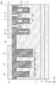
半導体装置100は、例えば、MOSFET(Metal Oxide Semiconductor Field Effect Transistor)である。
図1〜図4に表すように、半導体装置100は、n−形(第1導電形)半導体領域1(第1半導体領域)と、p形(第2導電形)ベース領域2(第2半導体領域)と、n+形ソース領域3(第3半導体領域)と、p+形コンタクト領域4と、n+形ドレイン領域5と、絶縁部10(第1絶縁部)と、フィールドプレート電極(以下、FP電極という)11と、ゲート電極12Aおよび12Bと、絶縁部20(第2絶縁部)と、絶縁部30(第3絶縁部)と、絶縁部40と、FP電極41Aおよび41Bと、絶縁層45と、ドレイン電極50と、ソース電極51(第1電極)と、ゲートパッド52(第2電極)と、を有する。
The
As shown in FIGS. 1 to 4, the
図1に表すように、半導体装置100の上面には、ソース電極51およびゲートパッド52が設けられている。ソース電極51とゲートパッド52とは、互いに離隔され、電気的に分離されている。
As shown in FIG. 1, a
図2に表すように、ソース電極51の下には、ゲートパッド52と電気的に接続された複数のゲート電極12Aおよび複数のゲート電極12Bが設けられている。複数のゲート電極12Aおよび複数のゲート電極12Bは、X方向に並べられ、各々がY方向に延びている。Z方向から見た場合に、ゲートパッド52は、Y方向において、ゲート電極12Bと並び、ゲート電極12Aとは並んでいない。このため、ゲート電極12BのY方向における長さは、ゲート電極12AのY方向における長さよりも短い。
以降では、ゲート電極12Aおよび12Bに共通する性質については、これらのゲート電極をまとめて「ゲート電極12」と称して説明する。
As shown in FIG. 2, below the
Hereinafter, the properties common to the
ゲートパッド52の下には、複数の絶縁部20がY方向に並べられている。各絶縁部20は、X方向に延びている。ゲート電極12Aの一部は、X方向において絶縁部20と並んでいる。また、ゲート電極12Bは、Y方向において、絶縁部20の一部と並んでいる。
Below the
絶縁部30は、Y方向に延びる第1絶縁部分30aと、X方向に延びる第2絶縁部分30bと、を有する。第1絶縁部分30aは、X方向において、複数の絶縁部20と複数のゲート電極12Aとの間に位置している。第2絶縁部分30bは、Y方向において、複数の絶縁部20と複数のゲート電極12Bとの間に位置している。
The insulating
FP電極41Aおよび41Bは、ソース電極51の下に設けられている。Z方向から見た場合に、ゲートパッド52は、Y方向において、FP電極41Bと並び、FP電極41Aと並んでいない。このため、FP電極41BのY方向における長さは、FP電極41AのY方向における長さよりも短い。
FP電極41Aの一部は、X方向において、ゲート電極12Aの一部と絶縁部30との間に位置している。FP電極41Bは、複数のゲート電極12Bの半導体装置外周側に位置している。ゲート電極12Bは、X方向において、FP電極41Aの一部とFP電極41Bとの間に設けられている。
以降では、FP電極41Aおよび41Bに共通する性質については、これらのFP電極をまとめて「FP電極41」と称して説明する。
The
Part of the
Hereinafter, the properties common to the
図3〜図5に表すように、半導体装置100の下面には、ドレイン電極50が設けられている。
n+形ドレイン領域5は、ドレイン電極50の上に設けられ、ドレイン電極50と電気的に接続されている。
n−形半導体領域1は、n+形ドレイン領域5の上に設けられている。
p形ベース領域2は、n−形半導体領域1の上に選択的に設けられている。
n+形ソース領域3およびp+形コンタクト領域4は、p形ベース領域2の上に選択的に設けられている。
As shown in FIGS. 3 to 5, a
The n + -
The n − type semiconductor region 1 is provided on the n + type drain region 5.
P-
The n + type source region 3 and the p + type contact region 4 are selectively provided on the p
FP電極11は、絶縁部10を介してn−形半導体領域1中に設けられている。
ゲート電極12は、絶縁部10を介してn−形半導体領域1中およびp形ベース領域2中に設けられている。ゲート電極12は、FP電極11の上に位置し、FP電極11と離間している。図4に表すように、FP電極11のY方向における端部は、Z方向に向けて屈曲しており、ゲート電極12とY方向において並んでいる。
The
ソース電極51の一部は、p形ベース領域2中に設けられ、n+形ソース領域3およびp+形コンタクト領域4と電気的に接続されている。ゲート電極12とソース電極51との間には、絶縁層45が設けられ、これらの電極は電気的に分離されている。
Part of the
FP電極41は、絶縁部40を介してn−形半導体領域1中およびp形ベース領域2中に設けられている。FP電極41は、ゲート電極12とX方向において離間している。
FP電極11および41は、ソース電極51またはゲートパッド52と電気的に接続されている。
絶縁部20および30は、p形ベース領域2、絶縁部10、およびゲート電極12と離間してn−形半導体領域1中に設けられている。また、絶縁部20と30は、n−形半導体領域1中で、X方向およびY方向において離間している。
絶縁部20および絶縁部30の周りのn−形半導体領域1は、絶縁層45に覆われており、ゲートパッド52は、絶縁層45の上に、ソース電極51と離間して設けられている。絶縁部10、20、および30は、絶縁層45によってつながっている。絶縁部10、20、および30と、絶縁層45と、は、例えば、一体に形成された絶縁膜である。
Insulating
The n − type semiconductor region 1 around the insulating
ここで、半導体装置100の動作について説明する。
ソース電極51に対して正の電圧がドレイン電極50に印加された状態で、ゲート電極12に閾値以上の電圧が印加されると、半導体装置がオン状態となる。このとき、絶縁部10近傍のp形ベース領域2にチャネル(反転層)が形成される。電子は、このチャネルを通ってn+形ソース領域3からn−形半導体領域1に流れ、n+形ドレイン領域5を通って排出される。
その後、ゲート電極12に印加される電圧が閾値よりも低くなると、p形ベース領域2におけるチャネルが消滅し、半導体装置がオフ状態になる。
Here, the operation of the
When a voltage equal to or higher than the threshold is applied to the
Thereafter, when the voltage applied to the
半導体装置100がオフ状態になると、FP電極11とドレイン電極50との間の電位差により、絶縁部10とn−形半導体領域1との界面からn−形半導体領域1に向けて空乏層が広がる。絶縁部10とn−形半導体領域1との界面から広がるこの空乏層により、半導体装置の耐圧を高めることができる。あるいは、半導体装置の耐圧が向上した分、n−形半導体領域1におけるn形不純物濃度を高め、半導体装置のオン抵抗を低減することができる。
When the
また、半導体装置100は、p形ベース領域2をアノード、n−形半導体領域1をカソードとするダイオードを内蔵している。このため、ドレイン電極50に対してソース電極51に正の電圧が印加された際には、ドレイン電極50からソース電極51へ順方向の電流が流れる。
Further, the
次に、各構成要素の材料の一例を説明する。
n−形半導体領域1、p形ベース領域2、n+形ソース領域3、p+形コンタクト領域4、およびn+形ドレイン領域5は、半導体材料として、シリコン、炭化シリコン、窒化ガリウム、またはガリウムヒ素を含む。半導体材料としてシリコンが用いられる場合、n形不純物として、ヒ素、リン、またはアンチモンを用いることができる。p形不純物として、ボロンを用いることができる。
FP電極11、ゲート電極12、およびFP電極41は、ポリシリコンなどの導電材料を含む。
絶縁部10、20、30、および40は、酸化シリコンなどの絶縁材料を含む。
ドレイン電極50、ソース電極51、およびゲートパッド52は、アルミニウムなどの金属を含む。
Next, an example of a material of each component will be described.
The n − -type semiconductor region 1, the p-
The
The insulating
The
ここで、本実施形態による効果を、図6〜図8を用いて説明する。
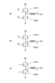
図6は、第1実施形態に係る半導体装置100が接続された電気回路の一例を表す回路図である。
図7は、第1実施形態に係る半導体装置におけるキャリアの流れを表す断面図である。
図8は、図6に表す電気回路中の半導体装置100−2における電流および電圧の波形を表すグラフである。
なお、図8において、実線は、ダイオードを流れる電流を表し、破線は、ソース電極51に対するドレイン電極50の電圧を表している。横軸は時間を表し、ダイオードの電流は順方向に流れる場合を正として表している。
Here, the effect of the present embodiment will be described with reference to FIGS.
FIG. 6 is a circuit diagram illustrating an example of an electric circuit to which the
FIG. 7 is a cross-sectional view illustrating the flow of carriers in the semiconductor device according to the first embodiment.
FIG. 8 is a graph showing current and voltage waveforms in the semiconductor device 100-2 in the electric circuit shown in FIG.
In FIG. 8, the solid line represents the current flowing through the diode, and the dashed line represents the voltage of the
図6に表す例では、本実施形態に係る2つの半導体装置100−1と100−2が用いられ、ハーフブリッジ回路が構成されている。図6(a)は、半導体装置100−1がオン状態、半導体装置100−2がオフ状態であり、半導体装置100−1に電流Iが流れている様子を表している。 In the example illustrated in FIG. 6, two semiconductor devices 100-1 and 100-2 according to the present embodiment are used, and a half bridge circuit is configured. FIG. 6A illustrates a state in which the semiconductor device 100-1 is in an on state and the semiconductor device 100-2 is in an off state, and the current I flows through the semiconductor device 100-1.
図6(a)に表す状態で、半導体装置100−1がターンオフされると、インダクタンスLによる誘導起電力が生じる。これにより、図6(b)に表すように、半導体装置100−2のダイオードに順方向の電流Iが流れる。このとき、正孔が、図7(a)に表すように、p形ベース領域2を通してソース電極51からn−形半導体領域1に注入される。
When the semiconductor device 100-1 is turned off in the state shown in FIG. 6A, an induced electromotive force is generated by the inductance L. Thereby, as shown in FIG. 6B, a forward current I flows through the diode of the semiconductor device 100-2. At this time, holes are injected from the
半導体装置100−2のダイオードに順方向電流が流れきると、半導体装置100−2の内部に蓄積されたキャリアが排出される。このとき、正孔は、図7(b)に表すように、p形ベース領域2を通してソース電極51へ排出される。半導体装置100−2からキャリアが排出されることで、図6(c)に表すように、半導体装置100−2には、ドレイン電極50からソース電極51に向かって逆回復電流が流れる。
When the forward current completely flows through the diode of the semiconductor device 100-2, the carriers accumulated inside the semiconductor device 100-2 are discharged. At this time, the holes are discharged to the
図8に表すように、タイミングT1で逆回復電流が流れきると、その後、半導体装置100−2のソース電極51に対するドレイン電極50の電圧Vが上昇していく。このとき、逆回復電流の減少の傾きdir/dtに応じて、電圧Vにサージ電圧Vsが発生する。dir/dtが大きいと、サージ電圧Vsも大きくなる。サージ電圧Vsが大きいと、n+形ソース領域3、p形ベース領域2、およびn−形半導体領域1から構成される寄生NPNトランジスタが動作し易くなる。寄生NPNトランジスタが動作すると、半導体装置内を大電流が流れ、半導体装置が破壊される可能性があるため、dir/dtは、小さいことが望ましい。
As shown in FIG. 8, when the reverse recovery current has completely flown at the timing T1, the voltage V of the
また、図8に表す蓄積電荷Qrrが大きく、一部のp形ベース領域2およびp+形コンタクト領域4に正孔が集中して流れると、寄生トランジスタのベース電位が上昇し、寄生トランジスタが動作する可能性がある。従って、dir/dtと同様に、蓄積電荷Qrrも少ないことが望ましい。
Further, when the accumulated charge Qrr shown in FIG. 8 is large and holes flow intensively in some of the p-
ダイオード動作時に注入された正孔の一部は、ゲートパッド52の下のn−形半導体領域1にも蓄積される。ゲートパッド52の下のn−形半導体領域1に蓄積された正孔は、逆回復動作時には、近くのp形ベース領域2に移動してソース電極51へ排出される。従って、ゲートパッド52下のn−形半導体領域1に近いp形ベース領域2には、他の部分に比べて多くの正孔が流れるため、より寄生NPNトランジスタが動作し易い。
このため、ゲートパッド52の下に蓄積される電荷Qrrの減少、およびゲートパッド52の下に蓄積されたキャリアによる逆回復時のdir/dtの減少が、寄生NPNトランジスタの動作の抑制に特に効果的である。
Some of the holes injected during the diode operation are also accumulated in the n − type semiconductor region 1 below the
Therefore, the reduction of the charge Qrr stored under the
この点について、本実施形態に係る半導体装置100のように、ゲートパッド52下のn−形半導体領域1中に絶縁部20を設けることで、ゲートパッド52の下のn−形半導体領域1の体積を減少させることができる。このため、ゲートパッド52の下に蓄積される電荷Qrrを減少させることができる。
In this regard, by providing the insulating
また、絶縁部20が複数設けられていることで、n−形半導体領域1に注入された正孔の一部が、絶縁部20同士の間に蓄積される。絶縁部20同士の間のn−形半導体領域1に蓄積された正孔は、逆回復動作時に、絶縁部20によってその移動が妨げられ、ソース電極51に向けて移動し難くなるため、逆回復に要する時間を長くし、dir/dtを小さくすることができる。
In addition, since the plurality of insulating
さらに、本実施形態に係る半導体装置100では、絶縁部30の第1絶縁部分30aが、複数の絶縁部20と複数のゲート電極12Aとの間をY方向に延びている。このような構造を採用することで、逆回復動作時に、絶縁部20同士の間のn−形半導体領域1に蓄積された正孔がソース電極51に向けて移動する際に、その移動が第1絶縁部分30aによって妨げられる。このため、逆回復に要する時間を長くし、dir/dtをさらに小さくすることができる。
Further, in the
すなわち、本実施形態によれば、絶縁部20および30が設けられることで、蓄積電荷Qrrを減少させ、かつdir/dtを小さくすることができ、これにより寄生NPNトランジスタが動作する可能性を低減することができる。
That is, according to the present embodiment, the provision of the insulating
ここで、図9を参照しつつ、本実施形態に係る半導体装置のより望ましい形態について説明する。
図9は、第1実施形態に係る半導体装置の平面図である。
第1絶縁部分30aは、X方向において、複数の絶縁部20と離間している。絶縁部30が第1絶縁部分30aのみを有する場合、絶縁部20同士の間に蓄積された正孔が、図9の矢印A1に表すように、絶縁部20と絶縁部30との隙間を流れ、p+形コンタクト領域4に流れる可能性がある。従って、絶縁部20と30との隙間を流れた正孔が、一部のp+形コンタクト領域4に集中して流れ、寄生NPNトランジスタが動作してしまう可能性がある。
Here, a more desirable mode of the semiconductor device according to the present embodiment will be described with reference to FIG.
FIG. 9 is a plan view of the semiconductor device according to the first embodiment.
The first insulating
絶縁部30が、第1絶縁部分30aに加えて、第2絶縁部分30bを有することで、矢印A1のように、絶縁部20と30との隙間を−Y方向に向けて流れる正孔を減少させることができる。このため、正孔が一部のp+形コンタクト領域4に集中して流れることを抑制し、寄生NPNトランジスタが動作する可能性をより一層低減させることが可能となる。
Since the insulating
また、逆回復動作時には、n−形半導体領域1の電位は、p形ベース領域2の電位よりも高く、ソース電極51に接続されたFP電極41Aの電位よりも高い。このため、絶縁部20および30とゲート電極12Aとの間に、FP電極41Aが設けられていることで、逆回復時にFP電極41A近傍を通った正孔が、FP電極41Aによってトラップすることができる。これにより、電荷Qrrを減少させ、寄生NPNトランジスタが動作する可能性をより一層低減させることが可能となる。
In the reverse recovery operation, the potential of n − type semiconductor region 1 is higher than the potential of p
(第1変形例)
図10は、第1実施形態の第1変形例に係る半導体装置110の一部を表す平面図である。
図10では、ソース電極51およびゲートパッド52が破線で表され、絶縁層45および各半導体領域が省略されている。
(First Modification)
FIG. 10 is a plan view illustrating a part of a
In FIG. 10, the
図2〜図4に表す半導体装置100では、ゲート電極12がY方向に延び、絶縁部20がX方向に延びている。これに対して、本変形例に係る半導体装置110では、ゲート電極12と絶縁部20とが、ともにY方向に延びている。
In the
半導体装置110では、半導体装置100と同様に、複数の絶縁部20が、ゲートパッド52の下に設けられている。また、絶縁部30の第2絶縁部分30bが、Y方向において、複数のゲート電極12Bと複数の絶縁部20との間に設けられている。
In the
このため、本変形例によれば、半導体装置100と同様に、ダイオード動作時における正孔の蓄積量および逆回復動作時における正孔の排出量を低減させることができる。
また、絶縁部30がY方向に延びる第1絶縁部分30aをさらに有することで、絶縁部20と第2絶縁部分30bの隙間を流れる正孔を減少させることができる点も同様である。
Therefore, according to the present modification, similarly to the
In addition, the fact that the insulating
ただし、ゲート電極12と絶縁部20が互いに異なる方向に延びている場合、絶縁部20同士の間に蓄積された正孔が、絶縁部20に沿ってソース電極51に向けて流れる際に、その流れがゲート電極12によって移動が妨げられる。従って、ゲート電極12と絶縁部20が互いに異なる方向に延びている場合、ゲート電極12と絶縁部20が同じ方向に延びている場合に比べて、電荷Qrrが減少し、寄生NPNトランジスタが動作する可能性をさらに低減することが可能である。
However, when the
(第2変形例)
図11は、第1実施形態の第2変形例に係る半導体装置120の一部を表す平面図である。
図12(a)は図11のE−E’断面図であり、図12(b)は図11のF−F’断面図である。
図13は、第1実施形態の第2変形例に係る半導体装置120の他の一例を表す部分拡大断面図である。
なお、図11では、ソース電極51およびゲートパッド52が破線で表され、絶縁層45および各半導体領域が省略されている。
(Second Modification)
FIG. 11 is a plan view illustrating a part of a
FIG. 12A is a sectional view taken along the line EE ′ of FIG. 11, and FIG. 12B is a sectional view taken along the line FF ′ of FIG.
FIG. 13 is a partially enlarged cross-sectional view illustrating another example of the
In FIG. 11, the
本変形例に係る半導体装置120では、図11に表すように、ゲート電極12と絶縁部20が互いに異なる方向に延びている。また、図12に表すように、絶縁部20の幅W2および絶縁部30の幅W3は、絶縁部10の幅W1よりも広い。
なお、ここでは、幅とは、それぞれの絶縁部が延びている方向に対して垂直な方向における、各絶縁部の長さを意味している。
In the
Here, the width means the length of each insulating portion in a direction perpendicular to the direction in which each insulating portion extends.
絶縁部20同士の間の距離D2および絶縁部20と30との間の距離D3は、絶縁部10同士の間の距離D1よりも短い。また、絶縁部20の下端および絶縁部30の下端は、絶縁部10の下端よりも下方に設けられている。
The distance D2 between the insulating
幅W2および幅W3を、幅W1よりも広くし、距離D2および距離D3を、距離D1よりも短くすることで、半導体装置100に比べて、ゲートパッド52の下のn−形半導体領域1の体積を小さくし、ゲートパッド52の下に蓄積される正孔の量を減少させることができる。
By making the width W2 and the width W3 wider than the width W1, and making the distance D2 and the distance D3 shorter than the distance D1, the n − type semiconductor region 1 below the
また、絶縁部20の下端および絶縁部30の下端は、絶縁部10の下端よりも下方に設けることで、ゲートパッド52の下のn−形半導体領域1の体積をさらに小さくし、図8に表す電荷Qrrを減少させることができる。加えて、絶縁部20同士の間に蓄積した正孔がソース電極51から排出されるまでの時間がより長くなるために、dir/dtをさらに小さくすることができる。
Further, by providing the lower end of the insulating
すなわち、本変形例に係る半導体装置120によれば、半導体装置100に比べて、寄生NPNトランジスタが動作する可能性をさらに低減することが可能である。
That is, according to the
なお、図13に表すように、絶縁部30の幅W3を幅W2よりも広くし、距離D3を距離D2より短くしてもよい。また、絶縁部30の下端の位置を絶縁部20の下端の位置よりも深くしてもよい。こうすることで、より一層、ゲートパッド52下の正孔の蓄積量およびソース電極51への正孔の排出量を減少させ、寄生NPNトランジスタが動作する可能性を低減させることが可能となる。
As shown in FIG. 13, the width W3 of the insulating
(第3変形例)
図14は、第1実施形態の第3変形例に係る半導体装置130の一部を表す平面図である。
図15は、図14のG−G’断面図である。
なお、図14では、ソース電極51およびゲートパッド52が破線で表され、絶縁層45および各半導体領域が省略されている。
(Third Modification)
FIG. 14 is a plan view illustrating a part of a
FIG. 15 is a sectional view taken along line GG ′ of FIG.
In FIG. 14, the
半導体装置130は、導電部21および導電部31をさらに備える点で、半導体装置100と異なる。導電部21は、絶縁部20中に設けられ、導電部31は、絶縁部30中に設けられている。
The
導電部21は、絶縁部20に沿ってX方向に延びている。
導電部31は、第1導電部分31aおよび第2導電部分31bを有する。第1導電部分31aは、第1絶縁部分30a中に設けられ、Y方向に延びている。第2導電部分31bは、第2絶縁部分30b中に設けられ、X方向に延びている。
The
The
導電部21および31は、ソース電極51およびゲートパッド52と電気的に分離されており、これらの導電部の電位は、フローティングである。
本変形例に係る半導体装置130においても、半導体装置100と同様に、電荷Qrrおよびdir/dtを減少させ、寄生NPNトランジスタが動作する可能性を低減させることが可能となる。
In the
また、導電部21および31をソース電極51およびゲートパッド52と電気的に分離することで、ソース電極51の容量およびゲートパッド52の容量の増加を抑え、半導体装置のスイッチング速度の低下を抑制することができる。
Further, by electrically separating the
なお、ここでは、半導体装置100に対して導電部21および31を設けた場合について説明したが、本変形例はこれに限られない。例えば、半導体装置110または120の絶縁部20中および絶縁部30中に、導電部21および31が設けられていてもよい。
Although the case where the
(第2実施形態)
図16は、第2実施形態に係る半導体装置200の一部を表す平面図である。
図17は、図16のH−H’断面図である。
なお、図16では、ソース電極51およびゲートパッド52が破線で表され、絶縁層45および各半導体領域が省略されている。
(2nd Embodiment)
FIG. 16 is a plan view illustrating a part of the
FIG. 17 is a sectional view taken along line HH ′ of FIG.
In FIG. 16, the
半導体装置200は、ゲートパッド52の下に設けられた絶縁部の構造が半導体装置100と異なる。
The
図16および図17に表すように、半導体装置200では、ゲートパッド52の下に、絶縁部22(第2絶縁部)、24(第3絶縁部)、および26が設けられている。絶縁部22、24、および26は、それぞれ環状に設けられ、n−形半導体領域1の一部を囲んでいる。絶縁部24は、絶縁部22の内側に設けられ、絶縁部26は、絶縁部24の内側に設けられている。
As shown in FIGS. 16 and 17, in the
所定の方向に延びる複数の絶縁部をゲートパッド52の下に設けた場合、絶縁部同士の隙間を通して、ゲートパッド52下の領域とソース電極51との間を正孔が移動する可能性がある。
これに対して、本実施形態に係る半導体装置200のように、ゲートパッド52の下に環状の絶縁部を設けることで、ゲートパッド52下の領域とソース電極51との間の正孔の移動をより一層抑制することが可能となる。このため、本実施形態によれば、第1実施形態に係る半導体装置に比べて、図8に表したdir/dtをより小さくし、寄生NPNトランジスタが動作する可能性をさらに低減することが可能である。
When a plurality of insulating portions extending in a predetermined direction are provided below the
On the other hand, by providing an annular insulating portion below the
なお、ゲートパッド52の下に設けられる環状の絶縁部の数は、図16に表す例よりも少なくても良いし、多くても良い。絶縁部の数は任意であり、適宜変更することが可能である。
Note that the number of annular insulating portions provided below the
(第1変形例)
図18は、第2実施形態の第1変形例に係る半導体装置210の一部を表す断面図である。
(First Modification)
FIG. 18 is a cross-sectional view illustrating a part of a
半導体装置210は、導電部23、25、および27をさらに備える点で、半導体装置200と異なる。
図18に表すように、導電部23、25、および27は、それぞれ、絶縁部22、24、および26の中に設けられている。導電部23、25、および27は、それぞれ環状に設けられており、n−形半導体領域1の一部を囲んでいる。
The
As shown in FIG. 18, the
導電部23、25、および27は、ソース電極51およびゲートパッド52と電気的に分離されており、これらの導電部の電位は、フローティングである。
The
本変形例においても、半導体装置200と同様に、電荷Qrrおよびdir/dtを減少させ、寄生NPNトランジスタが動作する可能性を低減することが可能である。
Also in the present modification, similarly to the
また、導電部23、25、および27をソース電極51およびゲートパッド52と電気的に分離することで、ソース電極51の容量およびゲートパッド52の容量の増加を抑え、半導体装置のスイッチング速度の低下を抑制することができる。
Further, by electrically separating the
(第2変形例)
図19は、第2実施形態の第2変形例に係る半導体装置220の一部を表す断面図である。
(Second Modification)
FIG. 19 is a cross-sectional view illustrating a part of a
半導体装置220は、絶縁部22、24、および26の構造が半導体装置200と異なる。
図19に表すように、絶縁部22の幅W2は、絶縁部24の幅W3よりも広く、幅W3は、絶縁部26の幅W4よりも広い。幅W2は、例えば、絶縁部10の幅と同じか、それよりも広い。
The
As shown in FIG. 19, the width W2 of the insulating
絶縁部22と24との間の距離D2は、絶縁部24と26との間の距離D3よりも狭い。距離D3は、絶縁部10同士の間の距離D1よりも狭い。また、絶縁部22の下端の位置は、絶縁部24の下端の位置よりも深く、絶縁部24の下端の位置は、絶縁部26の下端の位置よりも深い。絶縁部26の下端の位置は、例えば、絶縁部10の下端の位置と同じか、それよりも深い。
The distance D2 between the insulating
すなわち、絶縁部22、24、および26は、外側に向かうほど、幅が広く、下端の位置が深くなっている。外側の絶縁部の幅を広く、下端の位置を深くすることで、半導体装置200に比べて、ゲートパッド52下の領域とソース電極51との間の正孔の移動をより一層抑制し、dir/dtを小さくすることが可能となる。このため、本変形例によれば、寄生NPNトランジスタが動作する可能性をさらに低減させることが可能となる。
In other words, the insulating
なお、半導体装置220においても半導体装置210と同様に、絶縁部22、24、および26中に、それぞれ、導電部23、25、および27が設けられていてもよい。
In the
以上で説明した各実施形態における、各半導体領域の間の不純物濃度の相対的な高低については、例えば、SCM(走査型静電容量顕微鏡)を用いて確認することが可能である。なお、各半導体領域におけるキャリア濃度は、各半導体領域において活性化している不純物濃度と等しいものとみなすことができる。従って、各半導体領域の間のキャリア濃度の相対的な高低についても、SCMを用いて確認することができる。
また、各半導体領域における不純物濃度については、例えば、SIMS(二次イオン質量分析法)により測定することが可能である。
The relative level of the impurity concentration between the semiconductor regions in each of the embodiments described above can be confirmed using, for example, an SCM (scanning capacitance microscope). Note that the carrier concentration in each semiconductor region can be regarded as being equal to the impurity concentration activated in each semiconductor region. Therefore, the relative level of the carrier concentration between the semiconductor regions can be confirmed using the SCM.
The impurity concentration in each semiconductor region can be measured, for example, by SIMS (secondary ion mass spectrometry).
以上、本発明のいくつかの実施形態を説明したが、これらの実施形態は、例として提示したものであり、発明の範囲を限定することは意図していない。これら新規な実施形態は、その他の様々な形態で実施されることが可能であり、発明の要旨を逸脱しない範囲で、種々の省略、置き換え、変更を行うことができる。実施形態に含まれる、例えば、n−形半導体領域1、p形ベース領域2、n+形ソース領域3、p+形コンタクト領域4、n+形ドレイン領域5、絶縁部10、フィールドプレート電極11、ゲート電極12、絶縁部20、22、24、および26、導電部21、23、25、および27、絶縁部30、導電部31、絶縁部40、フィールドプレート電極41、絶縁層45、ドレイン電極50、ソース電極51、およびゲートパッド52などの各要素の具体的な構成に関しては、当業者が公知の技術から適宜選択することが可能である。これら実施形態やその変形は、発明の範囲や要旨に含まれるとともに、特許請求の範囲に記載された発明とその均等の範囲に含まれる。また、前述の各実施形態は、相互に組み合わせて実施することができる。
Although some embodiments of the present invention have been described above, these embodiments are presented as examples and are not intended to limit the scope of the invention. These new embodiments can be implemented in other various forms, and various omissions, replacements, and changes can be made without departing from the spirit of the invention. Included in the embodiment, for example, n -
100、110、120、130、200、210、220 半導体装置、 1 n−形半導体領域、 2 p形ベース領域、 3 n+形ソース領域、 4 p+形コンタクト領域、 5 n+形ドレイン領域、 10、20、22、24、26、30、40 絶縁部、 11、41A、41B フィールドプレート電極、 12A、12B ゲート電極、 21、23、25、27、31 導電部、 45 絶縁層、 50 ドレイン電極、 51 ソース電極、 52 ゲートパッド 100, 110, 120, 130, 200, 210, 220 semiconductor device, 1 n − type semiconductor region, 2 p type base region, 3 n + type source region, 4 p + type contact region, 5 n + type drain region, 10, 20, 22, 24, 26, 30, 40 insulating part, 11, 41A, 41B field plate electrode, 12A, 12B gate electrode, 21, 23, 25, 27, 31 conductive part, 45 insulating layer, 50 drain electrode , 51 source electrode, 52 gate pad
Claims (5)
前記第1半導体領域の上に選択的に設けられた第2導電形の第2半導体領域と、
前記第2半導体領域の上に選択的に設けられた第1導電形の第3半導体領域と、
前記第1半導体領域中および前記第2半導体領域中に第1絶縁部を介して設けられ、第1方向に延び、前記第1方向と交差する第2方向において複数設けられたゲート電極と、
前記第3半導体領域の上に設けられ、前記第3半導体領域と電気的に接続された第1電極と、
前記第1半導体領域中において前記複数のゲート電極と離間し、前記第2方向に延び、前記第1方向において複数設けられた第2絶縁部と、
前記第1方向に延びる第1絶縁部分を有し、前記第1絶縁部分が前記第2方向において前記複数のゲート電極と前記複数の第2絶縁部との間に位置し、前記第1半導体領域中において前記複数のゲート電極および前記複数の第2絶縁部と離間した第3絶縁部と、
前記複数の第2絶縁部および前記第3絶縁部の上に設けられ、前記複数のゲート電極と電気的に接続された第2電極と、
を備えた半導体装置。 A first semiconductor region of a first conductivity type;
A second semiconductor region of a second conductivity type selectively provided on the first semiconductor region;
A third semiconductor region of a first conductivity type selectively provided on the second semiconductor region;
A plurality of gate electrodes provided in the first semiconductor region and the second semiconductor region via a first insulating portion, extending in a first direction, and provided in a second direction intersecting the first direction ;
A first electrode provided on the third semiconductor region and electrically connected to the third semiconductor region;
A second insulating portion provided with a plurality in the in the first semiconductor region spaced apart from said plurality of gate electrodes extending before Symbol second direction, said first direction,
A first insulating portion extending in the first direction, wherein the first insulating portion is located between the plurality of gate electrodes and the plurality of second insulating portions in the second direction; A third insulating portion separated from the plurality of gate electrodes and the plurality of second insulating portions,
A second electrode provided on the plurality of second insulating portions and the third insulating portion and electrically connected to the plurality of gate electrodes;
A semiconductor device comprising:
前記第1半導体領域の上に選択的に設けられた第2導電形の第2半導体領域と、
前記第2半導体領域の上に選択的に設けられた第1導電形の第3半導体領域と、
前記第1半導体領域中および前記第2半導体領域中に第1絶縁部を介して設けられ、第1方向に延び、前記第1方向と交差する第2方向において複数設けられたゲート電極と、
前記第3半導体領域の上に設けられ、前記第3半導体領域と電気的に接続された第1電極と、
前記第1半導体領域中において前記複数のゲート電極と離間し、前記第2方向に延び、前記第1方向において複数設けられた第2絶縁部と、
前記第1方向に延びる第1絶縁部分および前記第2方向に延びる第2絶縁部分を有し、前記第1絶縁部分が前記第2方向において前記複数のゲート電極の一部と前記複数の第2絶縁部との間に位置し、前記第2絶縁部分が前記第1方向において前記複数のゲート電極の他の一部と前記複数の第2絶縁部との間に位置し、前記第1半導体領域中において前記複数のゲート電極および前記複数の第2絶縁部と離間した第3絶縁部と、
前記複数の第2絶縁部および前記第3絶縁部の上に設けられ、前記複数のゲート電極と電気的に接続された第2電極と、
を備えた半導体装置。 A first semiconductor region of a first conductivity type;
A second semiconductor region of a second conductivity type selectively provided on the first semiconductor region;
A third semiconductor region of a first conductivity type selectively provided on the second semiconductor region;
A plurality of gate electrodes provided in the first semiconductor region and the second semiconductor region via a first insulating portion, extending in a first direction, and provided in a second direction intersecting the first direction ;
A first electrode provided on the third semiconductor region and electrically connected to the third semiconductor region;
A second insulating portion that is separated from the plurality of gate electrodes in the first semiconductor region, extends in the second direction, and is provided in plurality in the first direction ;
A second insulating portion extending to the first insulating portion and the second direction extending in the first direction, wherein a portion of the first insulating portion before Symbol second direction odor Te before Symbol plurality of gate electrodes plurality the second is located between the insulating portion located between the second insulating portion and the second insulating portion of the other part of the plurality previous SL plurality of gate electrodes Te before Symbol first direction odor A third insulating portion separated from the plurality of gate electrodes and the plurality of second insulating portions in the first semiconductor region;
A second electrode provided on the plurality of second insulating portions and the third insulating portion and electrically connected to the plurality of gate electrodes;
A semiconductor device comprising:
前記第1半導体領域の上に選択的に設けられた第2導電形の第2半導体領域と、
前記第2半導体領域の上に選択的に設けられた第1導電形の第3半導体領域と、
前記第1半導体領域中および前記第2半導体領域中に第1絶縁部を介して設けられ、第1方向に延びるゲート電極と、
前記第3半導体領域の上に設けられ、前記第3半導体領域と電気的に接続された第1電極と、
前記第1半導体領域中において前記ゲート電極と離間し、前記第1方向と交差する第2方向に延びる第2絶縁部と、
前記第1方向に延びる第1絶縁部分を有し、前記第1絶縁部分が前記第2方向において前記ゲート電極と前記第2絶縁部との間に位置し、前記第1半導体領域中において前記ゲート電極および前記第2絶縁部と離間した第3絶縁部と、
前記第2絶縁部および前記第3絶縁部の上に設けられ、前記ゲート電極と電気的に接続された第2電極と、
前記第2絶縁部中に設けられ、前記第2方向に延び、前記第1電極および前記第2電極と電気的に分離された第1導電部と、
前記第1絶縁部分中を前記第1方向に延びる第1導電部分を有し、前記第3絶縁部中に設けられ、前記第1電極および前記第2電極と電気的に分離された第2導電部と、
を備えた半導体装置。 A first semiconductor region of a first conductivity type;
A second semiconductor region of a second conductivity type selectively provided on the first semiconductor region;
A third semiconductor region of a first conductivity type selectively provided on the second semiconductor region;
A gate electrode provided in the first semiconductor region and the second semiconductor region via a first insulating portion and extending in a first direction;
A first electrode provided on the third semiconductor region and electrically connected to the third semiconductor region;
A second insulating portion separated from the gate electrode in the first semiconductor region and extending in a second direction intersecting the first direction;
A first insulating portion extending in the first direction, wherein the first insulating portion is located between the gate electrode and the second insulating portion in the second direction, and wherein the gate is located in the first semiconductor region. A third insulating portion separated from the electrode and the second insulating portion;
A second electrode provided on the second insulating portion and the third insulating portion and electrically connected to the gate electrode;
A first conductive portion provided in the second insulating portion , extending in the second direction, and electrically separated from the first electrode and the second electrode ;
A second conductive portion having a first conductive portion extending in the first direction in the first insulating portion and provided in the third insulating portion and electrically separated from the first electrode and the second electrode; Department and
A semiconductor device comprising:
前記第1半導体領域の上に選択的に設けられた第2導電形の第2半導体領域と、
前記第2半導体領域の上に選択的に設けられた第1導電形の第3半導体領域と、
前記第1半導体領域中および前記第2半導体領域中に第1絶縁部を介して設けられ、第1方向に延び、前記第1方向と交差する第2方向において複数設けられたゲート電極と、
前記第3半導体領域の上に設けられ、前記第3半導体領域と電気的に接続された第1電極と、
前記第1半導体領域中において前記複数のゲート電極と離間し、前記第1方向に延び、前記第2方向において複数設けられた第2絶縁部と、
前記第1方向に延びる第1絶縁部分と前記第2方向に延びる第2絶縁部分を有し、前記第1絶縁部分が前記第2方向において前記複数のゲート電極の一部と前記複数の第2絶縁部との間に位置し、前記第2絶縁部分が前記第1方向において前記複数のゲート電極の他の一部と前記複数の第2絶縁部との間に位置し、前記第1半導体領域中において前記複数のゲート電極および前記複数の第2絶縁部と離間した第3絶縁部と、
前記複数の第2絶縁部および前記第3絶縁部の上に設けられ、前記複数のゲート電極と電気的に接続された第2電極と、
を備えた半導体装置。 A first semiconductor region of a first conductivity type;
A second semiconductor region of a second conductivity type selectively provided on the first semiconductor region;
A third semiconductor region of a first conductivity type selectively provided on the second semiconductor region;
A plurality of gate electrodes provided in the first semiconductor region and the second semiconductor region via a first insulating portion, extending in a first direction, and provided in a second direction intersecting the first direction;
A first electrode provided on the third semiconductor region and electrically connected to the third semiconductor region;
A second insulating portion that is separated from the plurality of gate electrodes in the first semiconductor region, extends in the first direction, and is provided in plurality in the second direction;
A first insulating portion extending in the first direction and a second insulating portion extending in the second direction, wherein the first insulating portion is configured to partially overlap the plurality of gate electrodes and the plurality of second electrodes in the second direction; The first semiconductor region, wherein the second semiconductor portion is located between the other portion of the plurality of gate electrodes and the plurality of second insulating portions in the first direction. a third insulating portion which is spaced apart from the plurality of second insulating portion of the gate electrode and before Kifuku number in the middle,
A second electrode provided on the plurality of second insulating portions and the third insulating portion and electrically connected to the plurality of gate electrodes;
A semiconductor device comprising:
前記第1半導体領域の上に選択的に設けられた第2導電形の第2半導体領域と、
前記第2半導体領域の上に選択的に設けられた第1導電形の第3半導体領域と、
前記第1半導体領域中および前記第2半導体領域中に第1絶縁部を介して設けられたゲート電極と、
前記第3半導体領域の上に設けられ、前記第3半導体領域と電気的に接続された第1電極と、
前記第1半導体領域中において前記ゲート電極と離間し、前記第1半導体領域の一部を囲む環状の第2絶縁部と、
前記第2絶縁部の上に設けられ、前記ゲート電極と電気的に接続された第2電極と、
前記第2絶縁部と離間して前記第1半導体領域中に設けられ、前記第2絶縁部の内側に位置し、前記第1半導体領域の一部を囲む環状の第3絶縁部と、
前記第2絶縁部中に設けられ、前記第1電極および前記第2電極と電気的に分離された環状の第1導電部と、
前記第3絶縁部中に設けられ、前記第1電極および前記第2電極と電気的に分離された環状の第2導電部と、
を備えた半導体装置。 A first semiconductor region of a first conductivity type;
A second semiconductor region of a second conductivity type selectively provided on the first semiconductor region;
A third semiconductor region of a first conductivity type selectively provided on the second semiconductor region;
A gate electrode provided in the first semiconductor region and the second semiconductor region via a first insulating portion;
A first electrode provided on the third semiconductor region and electrically connected to the third semiconductor region;
An annular second insulating portion spaced apart from the gate electrode in the first semiconductor region and surrounding a part of the first semiconductor region;
A second electrode provided on the second insulating portion and electrically connected to the gate electrode;
An annular third insulating portion provided in the first semiconductor region at a distance from the second insulating portion and located inside the second insulating portion and surrounding a part of the first semiconductor region;
An annular first conductive portion provided in the second insulating portion and electrically separated from the first electrode and the second electrode;
An annular second conductive portion provided in the third insulating portion and electrically separated from the first electrode and the second electrode;
A semiconductor device comprising:
Priority Applications (3)
| Application Number | Priority Date | Filing Date | Title |
|---|---|---|---|
| JP2016180766A JP6677613B2 (en) | 2016-09-15 | 2016-09-15 | Semiconductor device |
| US15/446,499 US10529805B2 (en) | 2016-09-15 | 2017-03-01 | Semiconductor device |
| CN201710377223.3A CN107833918B (en) | 2016-09-15 | 2017-05-25 | Semiconductor device with a plurality of semiconductor chips |
Applications Claiming Priority (1)
| Application Number | Priority Date | Filing Date | Title |
|---|---|---|---|
| JP2016180766A JP6677613B2 (en) | 2016-09-15 | 2016-09-15 | Semiconductor device |
Publications (3)
| Publication Number | Publication Date |
|---|---|
| JP2018046201A JP2018046201A (en) | 2018-03-22 |
| JP2018046201A5 JP2018046201A5 (en) | 2018-10-18 |
| JP6677613B2 true JP6677613B2 (en) | 2020-04-08 |
Family
ID=61560931
Family Applications (1)
| Application Number | Title | Priority Date | Filing Date |
|---|---|---|---|
| JP2016180766A Active JP6677613B2 (en) | 2016-09-15 | 2016-09-15 | Semiconductor device |
Country Status (3)
| Country | Link |
|---|---|
| US (1) | US10529805B2 (en) |
| JP (1) | JP6677613B2 (en) |
| CN (1) | CN107833918B (en) |
Families Citing this family (5)
| Publication number | Priority date | Publication date | Assignee | Title |
|---|---|---|---|---|
| JP6926012B2 (en) | 2018-02-14 | 2021-08-25 | 株式会社東芝 | Semiconductor device |
| JP7224979B2 (en) * | 2019-03-15 | 2023-02-20 | 株式会社東芝 | semiconductor equipment |
| JP7242485B2 (en) * | 2019-09-13 | 2023-03-20 | 株式会社東芝 | semiconductor equipment |
| CN115053352A (en) * | 2020-02-07 | 2022-09-13 | 罗姆股份有限公司 | Semiconductor device with a plurality of semiconductor chips |
| JP2022148177A (en) | 2021-03-24 | 2022-10-06 | 株式会社東芝 | Semiconductor device |
Family Cites Families (9)
| Publication number | Priority date | Publication date | Assignee | Title |
|---|---|---|---|---|
| JP4764998B2 (en) | 2003-11-14 | 2011-09-07 | 富士電機株式会社 | Semiconductor device |
| JP4498796B2 (en) * | 2004-03-29 | 2010-07-07 | トヨタ自動車株式会社 | Insulated gate semiconductor device and manufacturing method thereof |
| JP5048273B2 (en) | 2006-05-10 | 2012-10-17 | オンセミコンダクター・トレーディング・リミテッド | Insulated gate semiconductor device |
| JP6037499B2 (en) * | 2011-06-08 | 2016-12-07 | ローム株式会社 | Semiconductor device and manufacturing method thereof |
| JP5701913B2 (en) * | 2013-01-09 | 2015-04-15 | トヨタ自動車株式会社 | Semiconductor device |
| CN105103298B (en) * | 2013-03-31 | 2019-01-01 | 新电元工业株式会社 | Semiconductor device |
| JP6271155B2 (en) * | 2013-05-21 | 2018-01-31 | 株式会社東芝 | Semiconductor device |
| JP5842896B2 (en) * | 2013-11-12 | 2016-01-13 | トヨタ自動車株式会社 | Semiconductor device |
| WO2016006263A1 (en) * | 2014-07-11 | 2016-01-14 | 新電元工業株式会社 | Semiconductor device and method for producing semiconductor device |
-
2016
- 2016-09-15 JP JP2016180766A patent/JP6677613B2/en active Active
-
2017
- 2017-03-01 US US15/446,499 patent/US10529805B2/en active Active
- 2017-05-25 CN CN201710377223.3A patent/CN107833918B/en active Active
Also Published As
| Publication number | Publication date |
|---|---|
| CN107833918B (en) | 2021-03-16 |
| US10529805B2 (en) | 2020-01-07 |
| JP2018046201A (en) | 2018-03-22 |
| US20180076307A1 (en) | 2018-03-15 |
| CN107833918A (en) | 2018-03-23 |
Similar Documents
| Publication | Publication Date | Title |
|---|---|---|
| JP6677613B2 (en) | Semiconductor device | |
| US9362393B2 (en) | Vertical semiconductor device including element active portion and voltage withstanding structure portion, and method of manufacturing the vertical semiconductor device | |
| JP6197773B2 (en) | Semiconductor device | |
| JP5918288B2 (en) | Semiconductor device | |
| US10083957B2 (en) | Semiconductor device | |
| JP2014060362A (en) | Semiconductor device | |
| USRE48259E1 (en) | Semiconductor device | |
| JP2016163019A (en) | Semiconductor device | |
| JP6338776B2 (en) | Semiconductor device | |
| JP7208875B2 (en) | semiconductor equipment | |
| US9905689B2 (en) | Semiconductor device | |
| US20160260705A1 (en) | Semiconductor device | |
| JP2016058428A (en) | Semiconductor device | |
| JP5129943B2 (en) | Semiconductor device | |
| JP2012212842A (en) | Semiconductor device | |
| JP7227110B2 (en) | semiconductor equipment | |
| JP7204544B2 (en) | semiconductor equipment | |
| JP2016062975A (en) | Semiconductor device and method of manufacturing the same | |
| JP6408405B2 (en) | Semiconductor device | |
| JP4897029B2 (en) | Semiconductor device | |
| JP2014060299A (en) | Semiconductor device | |
| JP7352360B2 (en) | semiconductor equipment | |
| JP6450659B2 (en) | Semiconductor device | |
| JP6509674B2 (en) | Semiconductor device | |
| WO2012157025A1 (en) | Semiconductor device |
Legal Events
| Date | Code | Title | Description |
|---|---|---|---|
| A711 | Notification of change in applicant |
Free format text: JAPANESE INTERMEDIATE CODE: A712 Effective date: 20170911 |
|
| A711 | Notification of change in applicant |
Free format text: JAPANESE INTERMEDIATE CODE: A711 Effective date: 20170912 |
|
| A521 | Request for written amendment filed |
Free format text: JAPANESE INTERMEDIATE CODE: A523 Effective date: 20171031 |
|
| A521 | Request for written amendment filed |
Free format text: JAPANESE INTERMEDIATE CODE: A523 Effective date: 20180830 |
|
| A621 | Written request for application examination |
Free format text: JAPANESE INTERMEDIATE CODE: A621 Effective date: 20180830 |
|
| A977 | Report on retrieval |
Free format text: JAPANESE INTERMEDIATE CODE: A971007 Effective date: 20190412 |
|
| A131 | Notification of reasons for refusal |
Free format text: JAPANESE INTERMEDIATE CODE: A131 Effective date: 20190513 |
|
| A521 | Request for written amendment filed |
Free format text: JAPANESE INTERMEDIATE CODE: A523 Effective date: 20190708 |
|
| A131 | Notification of reasons for refusal |
Free format text: JAPANESE INTERMEDIATE CODE: A131 Effective date: 20191015 |
|
| A521 | Request for written amendment filed |
Free format text: JAPANESE INTERMEDIATE CODE: A523 Effective date: 20191125 |
|
| TRDD | Decision of grant or rejection written | ||
| A01 | Written decision to grant a patent or to grant a registration (utility model) |
Free format text: JAPANESE INTERMEDIATE CODE: A01 Effective date: 20200213 |
|
| A61 | First payment of annual fees (during grant procedure) |
Free format text: JAPANESE INTERMEDIATE CODE: A61 Effective date: 20200313 |
|
| R150 | Certificate of patent or registration of utility model |
Ref document number: 6677613 Country of ref document: JP Free format text: JAPANESE INTERMEDIATE CODE: R150 |