CN107833918B - Semiconductor device with a plurality of semiconductor chips - Google Patents
Semiconductor device with a plurality of semiconductor chips Download PDFInfo
- Publication number
- CN107833918B CN107833918B CN201710377223.3A CN201710377223A CN107833918B CN 107833918 B CN107833918 B CN 107833918B CN 201710377223 A CN201710377223 A CN 201710377223A CN 107833918 B CN107833918 B CN 107833918B
- Authority
- CN
- China
- Prior art keywords
- insulating
- semiconductor region
- insulating portion
- electrode
- semiconductor device
- Prior art date
- Legal status (The legal status is an assumption and is not a legal conclusion. Google has not performed a legal analysis and makes no representation as to the accuracy of the status listed.)
- Active
Links
- 239000004065 semiconductor Substances 0.000 title claims abstract description 210
- 230000003071 parasitic effect Effects 0.000 abstract description 21
- 238000009413 insulation Methods 0.000 description 16
- 238000011084 recovery Methods 0.000 description 12
- 238000012986 modification Methods 0.000 description 11
- 230000004048 modification Effects 0.000 description 11
- 239000012535 impurity Substances 0.000 description 9
- 239000000969 carrier Substances 0.000 description 5
- 239000000463 material Substances 0.000 description 3
- 238000010586 diagram Methods 0.000 description 2
- 230000005669 field effect Effects 0.000 description 2
- 229910044991 metal oxide Inorganic materials 0.000 description 2
- 150000004706 metal oxides Chemical class 0.000 description 2
- 238000001004 secondary ion mass spectrometry Methods 0.000 description 2
- 229910052710 silicon Inorganic materials 0.000 description 2
- 239000010703 silicon Substances 0.000 description 2
- JBRZTFJDHDCESZ-UHFFFAOYSA-N AsGa Chemical compound [As]#[Ga] JBRZTFJDHDCESZ-UHFFFAOYSA-N 0.000 description 1
- ZOXJGFHDIHLPTG-UHFFFAOYSA-N Boron Chemical compound [B] ZOXJGFHDIHLPTG-UHFFFAOYSA-N 0.000 description 1
- 229910002601 GaN Inorganic materials 0.000 description 1
- 229910001218 Gallium arsenide Inorganic materials 0.000 description 1
- JMASRVWKEDWRBT-UHFFFAOYSA-N Gallium nitride Chemical compound [Ga]#N JMASRVWKEDWRBT-UHFFFAOYSA-N 0.000 description 1
- OAICVXFJPJFONN-UHFFFAOYSA-N Phosphorus Chemical compound [P] OAICVXFJPJFONN-UHFFFAOYSA-N 0.000 description 1
- VYPSYNLAJGMNEJ-UHFFFAOYSA-N Silicium dioxide Chemical compound O=[Si]=O VYPSYNLAJGMNEJ-UHFFFAOYSA-N 0.000 description 1
- XUIMIQQOPSSXEZ-UHFFFAOYSA-N Silicon Chemical compound [Si] XUIMIQQOPSSXEZ-UHFFFAOYSA-N 0.000 description 1
- 229910052782 aluminium Inorganic materials 0.000 description 1
- XAGFODPZIPBFFR-UHFFFAOYSA-N aluminium Chemical compound [Al] XAGFODPZIPBFFR-UHFFFAOYSA-N 0.000 description 1
- 229910052787 antimony Inorganic materials 0.000 description 1
- WATWJIUSRGPENY-UHFFFAOYSA-N antimony atom Chemical compound [Sb] WATWJIUSRGPENY-UHFFFAOYSA-N 0.000 description 1
- 229910052785 arsenic Inorganic materials 0.000 description 1
- RQNWIZPPADIBDY-UHFFFAOYSA-N arsenic atom Chemical compound [As] RQNWIZPPADIBDY-UHFFFAOYSA-N 0.000 description 1
- 229910052796 boron Inorganic materials 0.000 description 1
- 230000015556 catabolic process Effects 0.000 description 1
- 239000004020 conductor Substances 0.000 description 1
- 230000003247 decreasing effect Effects 0.000 description 1
- 230000000694 effects Effects 0.000 description 1
- 238000002347 injection Methods 0.000 description 1
- 239000007924 injection Substances 0.000 description 1
- 239000011810 insulating material Substances 0.000 description 1
- 229910052751 metal Inorganic materials 0.000 description 1
- 239000002184 metal Substances 0.000 description 1
- 238000000034 method Methods 0.000 description 1
- 230000002093 peripheral effect Effects 0.000 description 1
- 229910052698 phosphorus Inorganic materials 0.000 description 1
- 239000011574 phosphorus Substances 0.000 description 1
- 229910021420 polycrystalline silicon Inorganic materials 0.000 description 1
- 229920005591 polysilicon Polymers 0.000 description 1
- 229910010271 silicon carbide Inorganic materials 0.000 description 1
- HBMJWWWQQXIZIP-UHFFFAOYSA-N silicon carbide Chemical compound [Si+]#[C-] HBMJWWWQQXIZIP-UHFFFAOYSA-N 0.000 description 1
- 229910052814 silicon oxide Inorganic materials 0.000 description 1
- 238000006467 substitution reaction Methods 0.000 description 1
Images


Classifications
-
- H—ELECTRICITY
- H01—ELECTRIC ELEMENTS
- H01L—SEMICONDUCTOR DEVICES NOT COVERED BY CLASS H10
- H01L29/00—Semiconductor devices adapted for rectifying, amplifying, oscillating or switching, or capacitors or resistors with at least one potential-jump barrier or surface barrier, e.g. PN junction depletion layer or carrier concentration layer; Details of semiconductor bodies or of electrodes thereof ; Multistep manufacturing processes therefor
- H01L29/02—Semiconductor bodies ; Multistep manufacturing processes therefor
- H01L29/06—Semiconductor bodies ; Multistep manufacturing processes therefor characterised by their shape; characterised by the shapes, relative sizes, or dispositions of the semiconductor regions ; characterised by the concentration or distribution of impurities within semiconductor regions
- H01L29/10—Semiconductor bodies ; Multistep manufacturing processes therefor characterised by their shape; characterised by the shapes, relative sizes, or dispositions of the semiconductor regions ; characterised by the concentration or distribution of impurities within semiconductor regions with semiconductor regions connected to an electrode not carrying current to be rectified, amplified or switched and such electrode being part of a semiconductor device which comprises three or more electrodes
- H01L29/1004—Base region of bipolar transistors
-
- H—ELECTRICITY
- H01—ELECTRIC ELEMENTS
- H01L—SEMICONDUCTOR DEVICES NOT COVERED BY CLASS H10
- H01L29/00—Semiconductor devices adapted for rectifying, amplifying, oscillating or switching, or capacitors or resistors with at least one potential-jump barrier or surface barrier, e.g. PN junction depletion layer or carrier concentration layer; Details of semiconductor bodies or of electrodes thereof ; Multistep manufacturing processes therefor
- H01L29/66—Types of semiconductor device ; Multistep manufacturing processes therefor
- H01L29/68—Types of semiconductor device ; Multistep manufacturing processes therefor controllable by only the electric current supplied, or only the electric potential applied, to an electrode which does not carry the current to be rectified, amplified or switched
- H01L29/76—Unipolar devices, e.g. field effect transistors
- H01L29/772—Field effect transistors
- H01L29/78—Field effect transistors with field effect produced by an insulated gate
- H01L29/7801—DMOS transistors, i.e. MISFETs with a channel accommodating body or base region adjoining a drain drift region
- H01L29/7802—Vertical DMOS transistors, i.e. VDMOS transistors
- H01L29/7813—Vertical DMOS transistors, i.e. VDMOS transistors with trench gate electrode, e.g. UMOS transistors
-
- H—ELECTRICITY
- H01—ELECTRIC ELEMENTS
- H01L—SEMICONDUCTOR DEVICES NOT COVERED BY CLASS H10
- H01L27/00—Devices consisting of a plurality of semiconductor or other solid-state components formed in or on a common substrate
- H01L27/02—Devices consisting of a plurality of semiconductor or other solid-state components formed in or on a common substrate including semiconductor components specially adapted for rectifying, oscillating, amplifying or switching and having at least one potential-jump barrier or surface barrier; including integrated passive circuit elements with at least one potential-jump barrier or surface barrier
- H01L27/04—Devices consisting of a plurality of semiconductor or other solid-state components formed in or on a common substrate including semiconductor components specially adapted for rectifying, oscillating, amplifying or switching and having at least one potential-jump barrier or surface barrier; including integrated passive circuit elements with at least one potential-jump barrier or surface barrier the substrate being a semiconductor body
- H01L27/06—Devices consisting of a plurality of semiconductor or other solid-state components formed in or on a common substrate including semiconductor components specially adapted for rectifying, oscillating, amplifying or switching and having at least one potential-jump barrier or surface barrier; including integrated passive circuit elements with at least one potential-jump barrier or surface barrier the substrate being a semiconductor body including a plurality of individual components in a non-repetitive configuration
- H01L27/0611—Devices consisting of a plurality of semiconductor or other solid-state components formed in or on a common substrate including semiconductor components specially adapted for rectifying, oscillating, amplifying or switching and having at least one potential-jump barrier or surface barrier; including integrated passive circuit elements with at least one potential-jump barrier or surface barrier the substrate being a semiconductor body including a plurality of individual components in a non-repetitive configuration integrated circuits having a two-dimensional layout of components without a common active region
- H01L27/0617—Devices consisting of a plurality of semiconductor or other solid-state components formed in or on a common substrate including semiconductor components specially adapted for rectifying, oscillating, amplifying or switching and having at least one potential-jump barrier or surface barrier; including integrated passive circuit elements with at least one potential-jump barrier or surface barrier the substrate being a semiconductor body including a plurality of individual components in a non-repetitive configuration integrated circuits having a two-dimensional layout of components without a common active region comprising components of the field-effect type
- H01L27/0623—Devices consisting of a plurality of semiconductor or other solid-state components formed in or on a common substrate including semiconductor components specially adapted for rectifying, oscillating, amplifying or switching and having at least one potential-jump barrier or surface barrier; including integrated passive circuit elements with at least one potential-jump barrier or surface barrier the substrate being a semiconductor body including a plurality of individual components in a non-repetitive configuration integrated circuits having a two-dimensional layout of components without a common active region comprising components of the field-effect type in combination with bipolar transistors
-
- H—ELECTRICITY
- H01—ELECTRIC ELEMENTS
- H01L—SEMICONDUCTOR DEVICES NOT COVERED BY CLASS H10
- H01L29/00—Semiconductor devices adapted for rectifying, amplifying, oscillating or switching, or capacitors or resistors with at least one potential-jump barrier or surface barrier, e.g. PN junction depletion layer or carrier concentration layer; Details of semiconductor bodies or of electrodes thereof ; Multistep manufacturing processes therefor
- H01L29/02—Semiconductor bodies ; Multistep manufacturing processes therefor
- H01L29/06—Semiconductor bodies ; Multistep manufacturing processes therefor characterised by their shape; characterised by the shapes, relative sizes, or dispositions of the semiconductor regions ; characterised by the concentration or distribution of impurities within semiconductor regions
- H01L29/0603—Semiconductor bodies ; Multistep manufacturing processes therefor characterised by their shape; characterised by the shapes, relative sizes, or dispositions of the semiconductor regions ; characterised by the concentration or distribution of impurities within semiconductor regions characterised by particular constructional design considerations, e.g. for preventing surface leakage, for controlling electric field concentration or for internal isolations regions
- H01L29/0642—Isolation within the component, i.e. internal isolation
- H01L29/0649—Dielectric regions, e.g. SiO2 regions, air gaps
-
- H—ELECTRICITY
- H01—ELECTRIC ELEMENTS
- H01L—SEMICONDUCTOR DEVICES NOT COVERED BY CLASS H10
- H01L29/00—Semiconductor devices adapted for rectifying, amplifying, oscillating or switching, or capacitors or resistors with at least one potential-jump barrier or surface barrier, e.g. PN junction depletion layer or carrier concentration layer; Details of semiconductor bodies or of electrodes thereof ; Multistep manufacturing processes therefor
- H01L29/02—Semiconductor bodies ; Multistep manufacturing processes therefor
- H01L29/06—Semiconductor bodies ; Multistep manufacturing processes therefor characterised by their shape; characterised by the shapes, relative sizes, or dispositions of the semiconductor regions ; characterised by the concentration or distribution of impurities within semiconductor regions
- H01L29/0684—Semiconductor bodies ; Multistep manufacturing processes therefor characterised by their shape; characterised by the shapes, relative sizes, or dispositions of the semiconductor regions ; characterised by the concentration or distribution of impurities within semiconductor regions characterised by the shape, relative sizes or dispositions of the semiconductor regions or junctions between the regions
- H01L29/0692—Surface layout
- H01L29/0696—Surface layout of cellular field-effect devices, e.g. multicellular DMOS transistors or IGBTs
-
- H—ELECTRICITY
- H01—ELECTRIC ELEMENTS
- H01L—SEMICONDUCTOR DEVICES NOT COVERED BY CLASS H10
- H01L29/00—Semiconductor devices adapted for rectifying, amplifying, oscillating or switching, or capacitors or resistors with at least one potential-jump barrier or surface barrier, e.g. PN junction depletion layer or carrier concentration layer; Details of semiconductor bodies or of electrodes thereof ; Multistep manufacturing processes therefor
- H01L29/40—Electrodes ; Multistep manufacturing processes therefor
- H01L29/402—Field plates
- H01L29/407—Recessed field plates, e.g. trench field plates, buried field plates
-
- H—ELECTRICITY
- H01—ELECTRIC ELEMENTS
- H01L—SEMICONDUCTOR DEVICES NOT COVERED BY CLASS H10
- H01L29/00—Semiconductor devices adapted for rectifying, amplifying, oscillating or switching, or capacitors or resistors with at least one potential-jump barrier or surface barrier, e.g. PN junction depletion layer or carrier concentration layer; Details of semiconductor bodies or of electrodes thereof ; Multistep manufacturing processes therefor
- H01L29/66—Types of semiconductor device ; Multistep manufacturing processes therefor
- H01L29/68—Types of semiconductor device ; Multistep manufacturing processes therefor controllable by only the electric current supplied, or only the electric potential applied, to an electrode which does not carry the current to be rectified, amplified or switched
- H01L29/76—Unipolar devices, e.g. field effect transistors
- H01L29/772—Field effect transistors
- H01L29/78—Field effect transistors with field effect produced by an insulated gate
- H01L29/7801—DMOS transistors, i.e. MISFETs with a channel accommodating body or base region adjoining a drain drift region
- H01L29/7802—Vertical DMOS transistors, i.e. VDMOS transistors
- H01L29/7803—Vertical DMOS transistors, i.e. VDMOS transistors structurally associated with at least one other device
- H01L29/7804—Vertical DMOS transistors, i.e. VDMOS transistors structurally associated with at least one other device the other device being a pn-junction diode
- H01L29/7805—Vertical DMOS transistors, i.e. VDMOS transistors structurally associated with at least one other device the other device being a pn-junction diode in antiparallel, e.g. freewheel diode
-
- H—ELECTRICITY
- H01—ELECTRIC ELEMENTS
- H01L—SEMICONDUCTOR DEVICES NOT COVERED BY CLASS H10
- H01L29/00—Semiconductor devices adapted for rectifying, amplifying, oscillating or switching, or capacitors or resistors with at least one potential-jump barrier or surface barrier, e.g. PN junction depletion layer or carrier concentration layer; Details of semiconductor bodies or of electrodes thereof ; Multistep manufacturing processes therefor
- H01L29/40—Electrodes ; Multistep manufacturing processes therefor
- H01L29/41—Electrodes ; Multistep manufacturing processes therefor characterised by their shape, relative sizes or dispositions
- H01L29/423—Electrodes ; Multistep manufacturing processes therefor characterised by their shape, relative sizes or dispositions not carrying the current to be rectified, amplified or switched
- H01L29/42312—Gate electrodes for field effect devices
- H01L29/42316—Gate electrodes for field effect devices for field-effect transistors
- H01L29/4232—Gate electrodes for field effect devices for field-effect transistors with insulated gate
- H01L29/42372—Gate electrodes for field effect devices for field-effect transistors with insulated gate characterised by the conducting layer, e.g. the length, the sectional shape or the lay-out
-
- H—ELECTRICITY
- H01—ELECTRIC ELEMENTS
- H01L—SEMICONDUCTOR DEVICES NOT COVERED BY CLASS H10
- H01L29/00—Semiconductor devices adapted for rectifying, amplifying, oscillating or switching, or capacitors or resistors with at least one potential-jump barrier or surface barrier, e.g. PN junction depletion layer or carrier concentration layer; Details of semiconductor bodies or of electrodes thereof ; Multistep manufacturing processes therefor
- H01L29/66—Types of semiconductor device ; Multistep manufacturing processes therefor
- H01L29/86—Types of semiconductor device ; Multistep manufacturing processes therefor controllable only by variation of the electric current supplied, or only the electric potential applied, to one or more of the electrodes carrying the current to be rectified, amplified, oscillated or switched
- H01L29/861—Diodes
- H01L29/8611—Planar PN junction diodes
Abstract
Embodiments of the invention provide a semiconductor device capable of suppressing an operation of a parasitic transistor. The semiconductor device of the embodiment has a1 st semiconductor region of a1 st conductivity type, a 2 nd semiconductor region of a 2 nd conductivity type, a 3 rd semiconductor region of the 1 st conductivity type, a gate electrode, a1 st electrode, a 2 nd insulating portion, a 3 rd insulating portion, and a 2 nd electrode. The gate electrode is provided in the 1 st semiconductor region and the 2 nd semiconductor region with the 1 st insulating portion interposed therebetween, and extends in the 1 st direction. The 1 st electrode is disposed over the 3 rd semiconductor region and electrically connected to the 3 rd semiconductor region. The 2 nd insulating portion is spaced apart from the gate electrode in the 1 st semiconductor region and extends in the 2 nd direction. The 3 rd insulating part has a1 st insulating portion extending in the 1 st direction. The 1 st insulating portion is located between the gate electrode and the 2 nd insulating portion in the 2 nd direction. The 2 nd electrode is disposed on the 2 nd insulating portion and the 3 rd insulating portion, and is electrically connected to the gate electrode.
Description
[ related applications ]
The present application has priority to application based on Japanese patent application No. 2016-. The present application incorporates the entire contents of the base application by reference thereto.
Technical Field
Embodiments of the present invention relate to a semiconductor device.
Background
A Semiconductor device such as a MOSFET (Metal Oxide Semiconductor Field Effect Transistor) has a parasitic Transistor. The parasitic transistor is preferably hard to operate.
Disclosure of Invention
The invention provides a semiconductor device capable of suppressing the operation of a parasitic transistor.
The semiconductor device of the embodiment has a1 st semiconductor region of a1 st conductivity type, a 2 nd semiconductor region of a 2 nd conductivity type, a 3 rd semiconductor region of the 1 st conductivity type, a gate electrode, a1 st electrode, a 2 nd insulating portion, a 3 rd insulating portion, and a 2 nd electrode. The 2 nd semiconductor region is selectively disposed over the 1 st semiconductor region. The 3 rd semiconductor region is selectively disposed over the 2 nd semiconductor region. The gate electrode is provided in the 1 st semiconductor region and the 2 nd semiconductor region with a1 st insulating portion interposed therebetween. The gate electrode extends in a1 st direction. The 1 st electrode is disposed over the 3 rd semiconductor region. The 1 st electrode is electrically connected to the 3 rd semiconductor region. The 2 nd insulating portion is spaced apart from the gate electrode in the 1 st semiconductor region. The 2 nd insulating portion extends in a 2 nd direction intersecting the 1 st direction. The 3 rd insulating part has a1 st insulating portion extending in the 1 st direction. The 1 st insulating portion of the 3 rd insulating portion is located between the gate electrode and the 2 nd insulating portion in the 2 nd direction. The 3 rd insulating portion is spaced apart from the gate electrode and the 2 nd insulating portion in the 1 st semiconductor region. The 2 nd electrode is provided on the 2 nd insulating portion and the 3 rd insulating portion. The 2 nd electrode is electrically connected to the gate electrode.
Drawings
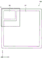
Fig. 1 is a plan view of a semiconductor device according to embodiment 1.
Fig. 2 is an enlarged plan view of a portion a of fig. 1.
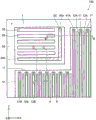
Fig. 3 is a sectional view B-B' of fig. 2.
Fig. 4 is a cross-sectional view of C-C' of fig. 2.
Fig. 5 is a cross-sectional view D-D' of fig. 2.
Fig. 6(a) to (c) are circuit diagrams showing an example of an electrical circuit connected to the semiconductor device of embodiment 1.
Fig. 7(a) and (b) are cross-sectional views showing the flow of carriers in the semiconductor device according to embodiment 1.
Fig. 8 is a graph showing waveforms of current and voltage in the semiconductor device in the electric circuit shown in fig. 6.
Fig. 9 is a plan view of semiconductor device 100 according to embodiment 1.
Fig. 10 is a plan view showing a part of a semiconductor device according to variation 1 of embodiment 1.
Fig. 11 is a plan view showing a part of a semiconductor device according to variation 2 of embodiment 1.
Fig. 12(a) is a sectional view of E-E 'of fig. 11, and fig. 12(b) is a sectional view of F-F' of fig. 11.
Fig. 13(a) and (b) are partially enlarged cross-sectional views showing another example of the semiconductor device according to variation 2 of embodiment 1.
Fig. 14 is a plan view showing a part of a semiconductor device according to variation 3 of embodiment 1.
Fig. 15 is a sectional view G-G' of fig. 14.
Fig. 16 is a plan view showing a part of the semiconductor device according to embodiment 2.
Fig. 17 is a sectional view H-H' of fig. 16.
Fig. 18 is a cross-sectional view showing a part of a semiconductor device according to variation 1 of embodiment 2.
Fig. 19 is a cross-sectional view showing a part of a semiconductor device according to variation 2 of embodiment 2.
Detailed Description
Embodiments of the present invention will be described below with reference to the drawings.
The drawings are schematic or conceptual, and the relationship between the thickness and the width of each portion, the ratio of the sizes of the portions, and the like are not necessarily the same as in the real case. Even when the same portions are shown, the sizes and ratios of the portions may be different from each other depending on the drawings.
In the description and drawings of the present application, the same elements as those already described are denoted by the same reference numerals, and detailed description thereof is appropriately omitted.
In the description of each embodiment, an XYZ orthogonal coordinate system is used. The direction from the drain electrode 50 to the source electrode 51 is defined as the Z direction. In addition, 2 directions perpendicular to the Z direction and orthogonal to each other are referred to as an X direction (2 nd direction) and a Y direction (1 st direction).
In the following description, n+、n-And p+、p-The notation of (1) indicates the relative high or low impurity concentration of each conductivity type. That is, notation with "+" means that the impurity concentration is relatively high compared to notation without "+" and without "-", and notation with "-" means that the impurity concentration is relatively low compared to notation without "+" and without "-".
In the embodiments described below, the p-type and the n-type of each semiconductor region may be reversed.
(embodiment 1)
An example of the semiconductor device according to embodiment 1 will be described with reference to fig. 1 to 5.
Fig. 1 is a plan view of a semiconductor device 100 according to embodiment 1.
Fig. 2 is an enlarged plan view of a portion a of fig. 1.
Fig. 3 is a sectional view B-B' of fig. 2.
Fig. 4 is a cross-sectional view of C-C' of fig. 2.
Fig. 5 is a cross-sectional view D-D' of fig. 2.
In fig. 2, the source electrode 51 and the gate pad 52 are indicated by broken lines, and the insulating layer 45, the p-type base region 2, and the n-type base region are omitted+And a source region 3.
The Semiconductor device 100 is, for example, a mosfet (metal Oxide Semiconductor Field Effect transistor).
As shown in FIGS. 1 to 4, the semiconductor device 100 has n-A type (1 st conductivity type) semiconductor region 1 (1 st semiconductor region), a p-type (2 nd conductivity type) base region 2 (2 nd semiconductor region), n+Type source region 3 (3 rd semiconductor region), p+ Type contact region 4, n+ Type drain region 5, insulating portion 10 (1 st insulating portion), field plate electrode (hereinafter, referred to as FP electrode) 11, gate electrodes 12A and 12B, insulating portion 20 (2 nd insulating portion), insulating portion 30 (3 rd insulating portion), insulating portion 40, FP electrodes 41A and 41B, insulating layer 45, drain electrode 50, source electrode 51 (1 st electrode), and gate pad 52 (2 nd electrode).
As shown in fig. 1, a source electrode 51 and a gate pad 52 are provided on the upper surface of the semiconductor device 100. The source electrode 51 and the gate pad 52 are electrically separated away from each other.
As shown in fig. 2, a plurality of gate electrodes 12A and a plurality of gate electrodes 12B electrically connected to the gate pads 52 are provided under the source electrodes 51. The plurality of gate electrodes 12A and the plurality of gate electrodes 12B are arranged in parallel in the X direction and each extend in the Y direction. The gate pad 52 is arranged side by side with the gate electrode 12B, not with the gate electrode 12A, in the Y direction when viewed from the Z direction. Therefore, the length of the gate electrode 12B in the Y direction is shorter than the length of the gate electrode 12A in the Y direction.
Hereinafter, the common property of the gate electrodes 12A and 12B will be described by collectively referring to the gate electrodes as "gate electrode 12".
Under the gate pad 52, a plurality of insulating portions 20 are arranged along the Y direction. Each of the insulating portions 20 extends in the X direction. A part of the gate electrode 12A is aligned with the insulating portion 20 in the X direction. The gate electrode 12B is arranged in parallel with a part of the insulating portion 20 in the Y direction.
The insulating portion 30 has a1 st insulating portion 30a extending in the Y direction and a 2 nd insulating portion 30b extending in the X direction. The 1 st insulating portion 30a is located between the plurality of insulating portions 20 and the plurality of gate electrodes 12A in the X direction. The 2 nd insulating portion 30B is located between the plurality of insulating portions 20 and the plurality of gate electrodes 12B in the Y direction.
The FP electrodes 41A and 41B are disposed below the source electrode 51. The gate pad 52 is arranged in the Y direction along the FP electrode 41B, not along the FP electrode 41A when viewed from the Z direction. Therefore, the length of the FP electrode 41B in the Y direction is shorter than the length of the FP electrode 41A in the Y direction.
A part of the FP electrode 41A is located between a part of the gate electrode 12A and the insulating portion 30 in the X direction. The FP electrode 41B is located on the outer peripheral side of the semiconductor device of the plurality of gate electrodes 12B. The gate electrode 12B is provided between a part of the FP electrode 41A and the FP electrode 41B in the X direction.
Hereinafter, the properties common to the FP electrodes 41A and 41B will be described as "FP electrode 41" collectively.
As shown in fig. 3 to 5, a drain electrode 50 is provided on the lower surface of the semiconductor device 100.
n+The type drain region 5 is disposed over the drain electrode 50 and electrically connected to the drain electrode 50.
n-The type semiconductor region 1 is arranged at n+Over the type drain region 5.
The p-type base region 2 is selectively arrangedAt n-Over the type semiconductor region 1.
n+ Type source regions 3 and p+A type contact region 4 is selectively provided over the p-type base region 2.
A gate electrode 12 is provided at n via an insulating portion 10-In the type semiconductor region 1 and in the p-type base region 2. The gate electrode 12 is located above the FP electrode 11 and spaced apart from the FP electrode 11. As shown in fig. 4, the FP electrode 11 has its end in the Y direction turned in the Z direction and is aligned with the gate electrode 12 in the Y direction.
A part of the source electrode 51 is arranged in the p-type base region 2 and is connected to n+ Type source regions 3 and p+The type contact regions 4 are electrically connected. Between the gate electrode 12 and the source electrode 51, an insulating layer 45 is provided, and these electrodes are electrically separated.
The FP electrodes 11 and 41 are electrically connected to the source electrode 51 or the gate pad 52.
The insulating parts 20 and 30 are provided at n intervals from the p-type base region 2, the insulating part 10, and the gate electrode 12-In the type semiconductor region 1. In addition, the insulation parts 20 and 30 are at n-The semiconductor regions 1 are spaced apart in the X-direction and the Y-direction.
Here, the operation of the semiconductor device 100 will be described.
When a voltage equal to or higher than a threshold value is applied to the gate electrode 12 in a state where a positive voltage is applied to the drain electrode 50 with respect to the source electrode 51, the semiconductor device is turned on. At this time, the insulation partThe p-type base region 2 near 10 forms a channel (inversion layer). Electrons passing through the channel from n+The source region 3 flows to n- Type semiconductor region 1, and passing n+Drain region 5.
Thereafter, if the voltage applied to the gate electrode 12 is lower than the threshold value, the channel in the p-type base region 2 is annihilated, and the semiconductor device becomes an off state.
If the semiconductor device 100 is turned off, a depletion layer is formed from the insulating portion 10 and n due to a potential difference between the FP electrode 11 and the drain electrode 50-Interface of type semiconductor region 1 is oriented to n-The type semiconductor region 1 is enlarged. Using the slave insulating parts 10 and n-The depletion layer having an enlarged interface with the type semiconductor region 1 can improve the breakdown voltage of the semiconductor device. Alternatively, n can be increased to a degree corresponding to the increase in withstand voltage of the semiconductor device-The n-type impurity concentration in the type semiconductor region 1, thereby reducing the on-resistance of the semiconductor device.
Next, an example of the material of each component will be described.
n- Type semiconductor region 1, p-type base region 2, n+ Type source region 3, p+ Type contact region 4, and n+The type drain region 5 includes silicon, silicon carbide, gallium nitride, or gallium arsenide as a semiconductor material. In the case of using silicon as a semiconductor material, arsenic, phosphorus, or antimony may be used as an n-type impurity. Boron may be used as the p-type impurity.
The FP electrode 11, the gate electrode 12, and the FP electrode 41 include a conductive material such as polysilicon.
The insulating portions 10, 20, 30, and 40 include an insulating material such as silicon oxide.
The drain electrode 50, the source electrode 51, and the gate pad 52 include a metal such as aluminum.
Here, the effects achieved by the present embodiment will be described with reference to fig. 6 to 8.
Fig. 6 is a circuit diagram showing an example of an electric circuit connected to the semiconductor device 100 according to embodiment 1.
Fig. 7 is a cross-sectional view showing a flow of carriers in the semiconductor device according to embodiment 1.
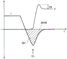
Fig. 8 is a graph showing waveforms of current and voltage in the semiconductor device 100-2 in the electric circuit shown in fig. 6.
In fig. 8, the solid line indicates the current flowing through the diode, and the broken line indicates the voltage of the drain electrode 50 with respect to the source electrode 51. The horizontal axis represents time, and the current of the diode is represented as positive when flowing in the forward direction.
In the example shown in fig. 6, a half-bridge circuit is formed using 2 semiconductor devices 100-1 and 100-2 according to this embodiment. Fig. 6(a) shows a case where the semiconductor device 100-1 is in an on state and the semiconductor device 100-2 is in an off state, and a current I flows in the semiconductor device 100-1.
If the semiconductor device 100-1 is turned off in the state shown in fig. 6(a), an induced electromotive force based on the inductance L is generated. As a result, a forward current I flows through the diode of the semiconductor device 100-2, as shown in fig. 6 (b). At this time, holes are injected from the source electrode 51 to n through the p-type base region 2 as shown in FIG. 7(a)-And a type semiconductor region 1.
If the flow of the forward current to the diode of the semiconductor device 100-2 is finished, carriers stored inside the semiconductor device 100-2 are discharged. At this time, as shown in fig. 7(b), holes are discharged to the source electrode 51 through the p-type base region 2. Carriers are discharged from the semiconductor device 100-2, and thus, as shown in fig. 6(c), a reverse recovery current flows from the drain electrode 50 to the source electrode 51 in the semiconductor device 100-2.
As shown in fig. 8, if the flow of the reverse recovery current is ended at the timing T1, thereafter, the voltage V of the drain electrode 50 with respect to the source electrode 51 of the semiconductor device 100-2 starts to rise. At this time, the decreasing slope dir/d corresponding to the reverse recovery currentt, a surge voltage Vs is generated in the voltage V. If dir/dt is large, the surge voltage Vs is also large. If the surge voltage Vs is large, n is+A source region 3, a base region 2, and n-The parasitic NPN transistor formed in the semiconductor region 1 is easy to operate. If the parasitic NPN transistor operates, a large current flows through the semiconductor device, and the semiconductor device may be damaged, and thus dir/dt is preferably small.
In addition, if the stored charge Qrr is large as shown in FIG. 8, holes flow intensively to a portion of the p-type base region 2 and p+The type contact region 4 may increase the base potential of the parasitic transistor, and the parasitic transistor may operate. Therefore, it is preferable that the stored charge Qrr is small as in dir/dt.
A portion of the holes injected during diode operation are also stored under the gate pad 52 as n-And a type semiconductor region 1. N stored under the gate pad 52-During the reverse recovery operation, holes in the type semiconductor region 1 move to the neighboring p-type base region 2 and are discharged to the source electrode 51. Thus, n is under the gate pad 52-The parasitic NPN transistor is more likely to operate because more holes flow in the p-type base region 2 near the p-type semiconductor region 1 than in other portions.
Therefore, reducing the charge Qrr stored under the gate pad 52 and reducing the reverse recovery dir/dt of the carriers stored under the gate pad 52 are particularly effective for suppressing the operation of the parasitic NPN transistor.
In this regard, as in the semiconductor device 100 of the present embodiment, n is below the gate pad 52-The insulating portion 20 is provided in the type semiconductor region 1, whereby n under the gate pad 52 can be reduced-Volume of the type semiconductor region 1. Therefore, the charge Qrr stored under the gate pad 52 can be reduced.
Furthermore, by providing a plurality of insulating portions 20, the injection into n can be performed-A part of holes of the type semiconductor region 1 are stored between the insulating portions 20. N between the insulating parts 20 is stored-Since the holes in the type semiconductor region 1 are prevented from moving toward the source electrode 51 by the insulating portion 20 during the reverse recovery operation, the time required for the reverse recovery can be extended and dir/dt can be reduced.
Further, in the semiconductor device 100 of the present embodiment, the 1 st insulating portion 30a of the insulating portion 30 extends in the Y direction between the plurality of insulating portions 20 and the plurality of gate electrodes 12A. By adopting such a configuration, n stored between the insulating parts 20 at the time of the reverse recovery action-When the holes of the type semiconductor region 1 move toward the source electrode 51, the movement thereof is hindered by the 1 st insulating portion 30 a. Therefore, the time required for reverse recovery can be extended, and dir/dt can be further reduced.
That is, according to the present embodiment, by providing the insulating portions 20 and 30, the stored charge Qrr can be reduced and dir/dt can be reduced, thereby reducing the possibility of the parasitic NPN transistor operation.
Here, a more preferable embodiment of the semiconductor device of the present embodiment will be described with reference to fig. 9.
Fig. 9 is a plan view of the semiconductor device according to embodiment 1.
The 1 st insulating portion 30a is spaced apart from the plurality of insulating portions 20 in the X direction. In the case where the insulating portion 30 has only the 1 st insulating portion 30a, there are possibilities as follows: the holes accumulated between the insulating portions 20 flow through the gap between the insulating portions 20 and 30 and p as indicated by an arrow a1 in fig. 9+And a type contact region 4. Therefore, holes flowing through the gap between the insulating portions 20 and 30 flow intensively to the portion p+The type contact region 4, thereby parasitic the possibility of the NPN type transistor operation.
By providing the insulating portion 30 with the 2 nd insulating portion 30b in addition to the 1 st insulating portion 30a, holes flowing in the-Y direction in the gap between the insulating portions 20 and 30 as indicated by the arrow a1 can be reduced. Therefore, the concentrated flow of holes to the portion p can be suppressed+The possibility of operation of the parasitic NPN transistor can be further reduced by the contact region 4.
Also, in the reverse recovery operation, n-The potential of the type semiconductor region 1 is higher than that of the p-type base region 2 and also higher than that of the FP electrode 41A connected to the source electrode 51. Therefore, by providing the FP electrode 41A between the insulating portions 20 and 30 and the gate electrode 12A, holes passing through the vicinity of the FP electrode 41A at the time of reverse recovery can be trapped by the FP electrode 41A. This can reduce the charge Qrr, and can further reduce the possibility of the parasitic NPN transistor operating.
(modification 1)
Fig. 10 is a plan view showing a part of a semiconductor device 110 according to variation 1 of embodiment 1.
In fig. 10, the source electrode 51 and the gate pad 52 are indicated by broken lines, and the insulating layer 45 and the semiconductor regions are omitted.
In the semiconductor device 100 shown in fig. 2 to 4, the gate electrode 12 extends in the Y direction, and the insulating portion 20 extends in the X direction. In contrast, in the semiconductor device 110 of the present modification, both the gate electrode 12 and the insulating portion 20 extend in the Y direction.
In the semiconductor device 110, the plurality of insulating portions 20 are provided under the gate pad 52, as in the semiconductor device 100. In addition, the 2 nd insulating portion 30B of the insulating portion 30 is disposed between the plurality of gate electrodes 12B and the plurality of insulating portions 20 in the Y direction.
Therefore, according to this modification, similarly to the semiconductor device 100, the hole storage amount during the diode operation and the hole discharge amount during the reverse recovery operation can be reduced.
In addition, the same is true in that holes flowing through the gap between the insulating portion 20 and the 2 nd insulating portion 30b can be reduced by providing the insulating portion 30 with the 1 st insulating portion 30a extending in the Y direction.
However, in the case where the gate electrode 12 and the insulating portion 20 extend in different directions from each other, when holes stored between the insulating portions 20 flow toward the source electrode 51 along the insulating portion 20, the movement of the hole flow is hindered by the gate electrode 12. Therefore, when the gate electrode 12 and the insulating portion 20 extend in different directions from each other, the charge Qrr can be reduced as compared with the case where the gate electrode 12 and the insulating portion 20 extend in the same direction, and the possibility of the parasitic NPN transistor operation can be further reduced.
(modification 2)
Fig. 11 is a plan view showing a part of a semiconductor device 120 according to variation 2 of embodiment 1.
Fig. 12(a) is a sectional view of E-E 'of fig. 11, and fig. 12(b) is a sectional view of F-F' of fig. 11.
Fig. 13 is a partially enlarged cross-sectional view showing another example of a semiconductor device 120 according to variation 2 of embodiment 1.
In fig. 11, the source electrode 51 and the gate pad 52 are indicated by broken lines, and the insulating layer 45 and the semiconductor regions are omitted.
In the semiconductor device 120 of the present modification example, as shown in fig. 11, the gate electrode 12 and the insulating portion 20 extend in different directions from each other. As shown in fig. 12, width W2 of insulation portion 20 and width W3 of insulation portion 30 are wider than width W1 of insulation portion 10.
The width here indicates the length of each insulating portion in the direction perpendicular to the extending direction of each insulating portion.
The distance D2 between the insulation parts 20 and the distance D3 between the insulation parts 20 and 30 are shorter than the distance D1 between the insulation parts 10. The lower ends of the insulating portions 20 and 30 are disposed below the lower end of the insulating portion 10.
By making the width W2 and the width W3 wider than the width W1 and making the distance D2 and the distance D3 shorter than the distance D1, n under the gate pad 52 can be made smaller than that of the semiconductor device 100-The volume of the type semiconductor region 1, thereby reducing the amount of holes stored under the gate pad 52.
In addition, by providing the lower end of the insulating portion 20 and the lower end of the insulating portion 30 below the lower end of the insulating portion 10, n below the gate pad 52 can be further reduced-The volume of the type semiconductor region 1 can reduce the charge Qrr shown in fig. 8. In addition, the time until the holes accumulated between the insulating portions 20 are discharged from the source electrode 51 becomes longerSince the length is long, dir/dt can be further reduced.
That is, according to the semiconductor device 120 of the present variation, the possibility of the parasitic NPN transistor operating can be further reduced as compared with the semiconductor device 100.
As shown in fig. 13, the width W3 of the insulating portion 30 may be made wider than the width W2, and the distance D3 may be made shorter than the distance D2. The lower end of the insulating portion 30 may be located deeper than the lower end of the insulating portion 20. By such an arrangement, the amount of holes stored under the gate pad 52 and the amount of holes discharged toward the source electrode 51 can be further reduced, and the possibility of the parasitic NPN transistor operation can be reduced.
(modification 3)
Fig. 14 is a plan view showing a part of a semiconductor device 130 according to variation 3 of embodiment 1.
Fig. 15 is a sectional view G-G' of fig. 14.
In fig. 14, the source electrode 51 and the gate pad 52 are indicated by broken lines, and the insulating layer 45 and the semiconductor regions are omitted.
The semiconductor device 130 is different from the semiconductor device 100 in that it further includes the conductive portion 21 and the conductive portion 31. The conductive portion 21 is provided in the insulating portion 20, and the conductive portion 31 is provided in the insulating portion 30.
The conductive portion 21 extends in the X direction along the insulating portion 20.
The conductive portion 31 has a1 st conductive portion 31a and a 2 nd conductive portion 31 b. The 1 st conductive portion 31a is disposed in the 1 st insulating portion 30a, and extends in the Y direction. The 2 nd conductive portion 31b is disposed in the 2 nd insulating portion 30b, and extends in the X direction.
The conductive portions 21 and 31 are electrically separated from the source electrode 51 and the gate pad 52, and the potentials of these conductive portions are floating.
In the semiconductor device 130 of the present variation, as in the semiconductor device 100, the electric charges Qrr and dir/dt can be reduced, and the possibility of the parasitic NPN transistor operating can be reduced.
Further, by electrically separating the conductive portions 21 and 31 from the source electrode 51 and the gate pad 52, it is possible to suppress an increase in the capacitance of the source electrode 51 and the capacitance of the gate pad 52, and to suppress a decrease in the switching speed of the semiconductor device.
Here, although the case where the conductive portions 21 and 31 are provided in the semiconductor device 100 has been described, the present modification is not limited to this. For example, the conductive portions 21 and 31 may be provided in the insulating portion 20 and the insulating portion 30 of the semiconductor device 110 or 120.
(embodiment 2)
Fig. 16 is a plan view showing a part of a semiconductor device 200 according to embodiment 2.
Fig. 17 is a sectional view H-H' of fig. 16.
In fig. 16, the source electrode 51 and the gate pad 52 are indicated by broken lines, and the insulating layer 45 and the semiconductor regions are omitted.
The semiconductor device 200 is different from the semiconductor device 100 in the structure of the insulating portion provided under the gate pad 52.
As shown in fig. 16 and 17, in the semiconductor device 200, the insulating portions 22 (2 nd insulating portion), 24 (3 rd insulating portion), and 26 are provided under the gate pad 52. The insulating portions 22, 24 and 26 are respectively configured in a ring shape and surround n-A portion of the type semiconductor region 1. The insulating portion 24 is disposed inside the insulating portion 22, and the insulating portion 26 is disposed inside the insulating portion 24.
In the case where a plurality of insulating portions extending in a predetermined direction are provided under the gate pad 52, holes may move between the region under the gate pad 52 and the source electrode 51 through the gaps between the insulating portions.
In contrast, by providing an annular insulating portion under the gate pad 52 as in the semiconductor device 200 of the present embodiment, it is possible to further suppress the movement of holes between the region under the gate pad 52 and the source electrode 51. Therefore, according to this embodiment, dir/dt shown in fig. 8 can be made smaller than that of the semiconductor device according to embodiment 1, and the possibility of the parasitic NPN transistor operating can be further reduced.
The number of annular insulating portions provided under the gate pad 52 may be smaller or larger than the example shown in fig. 16. The number of the insulating portions is arbitrary and can be changed as appropriate.
(modification 1)
Fig. 18 is a cross-sectional view showing a part of a semiconductor device 210 according to variation 1 of embodiment 2.
The semiconductor device 210 is different from the semiconductor device 200 in that it further includes conductive portions 23, 25, and 27.
As shown in fig. 18, the conductive portions 23, 25, and 27 are provided in the insulating portions 22, 24, and 26, respectively. The conductive parts 23, 25 and 27 are respectively configured into a ring shape and surround n-A portion of the type semiconductor region 1.
The conductive portions 23, 25, and 27 are electrically separated from the source electrode 51 and the gate pad 52, and the potentials of these conductive portions are floating.
In this variation as well, as in the case of the semiconductor device 200, the electric charges Qrr and dir/dt can be reduced, and the possibility of the parasitic NPN transistor operating can be reduced.
Further, by electrically separating the conductive portions 23, 25, and 27 from the source electrode 51 and the gate pad 52, an increase in the capacitance of the source electrode 51 and an increase in the capacitance of the gate pad 52 can be suppressed, and a decrease in the switching speed of the semiconductor device can be suppressed.
(modification 2)
Fig. 19 is a cross-sectional view showing a part of a semiconductor device 220 according to variation 2 of embodiment 2.
The semiconductor device 220 is different from the semiconductor device 200 in the structure of the insulating portions 22, 24, and 26.
As shown in fig. 19, width W2 of insulation 22 is wider than width W3 of insulation 24, and width W3 is wider than width W4 of insulation 26. The width W2 is, for example, the same as or wider than the width of the insulating portion 10.
The distance D2 between insulation portions 22 and 24 is narrower than the distance D3 between insulation portions 24 and 26. The distance D3 is narrower than the distance D1 between the insulation parts 10. The lower end of the insulating portion 22 is located deeper than the lower end of the insulating portion 24, and the lower end of the insulating portion 24 is located deeper than the lower end of the insulating portion 26. The position of the lower end of the insulating portion 26 is, for example, the same as or deeper than the position of the lower end of the insulating portion 10.
That is, the width of the insulating portions 22, 24, and 26 increases toward the outside, and the lower end thereof is located deeper. By increasing the width of the outer insulating portion and increasing the position of the lower end, it is possible to further suppress the movement of holes between the region under the gate pad 52 and the source electrode 51, and to reduce dir/dt, as compared with the semiconductor device 200. Therefore, according to this modification, the possibility of the parasitic NPN transistor operating can be further reduced.
In the semiconductor device 220, the conductive portions 23, 25, and 27 may be provided in the insulating portions 22, 24, and 26, respectively, as in the semiconductor device 210.
The relative levels of the impurity concentrations between the semiconductor regions in the above-described embodiments can be confirmed, for example, by using SCM (scanning capacitance microscope). The carrier concentration in each semiconductor region can be considered to be equal to the impurity concentration activated in each semiconductor region. Therefore, the relative level of the carrier concentration between the semiconductor regions can also be confirmed using SCM.
The impurity concentration in each semiconductor region can be measured by, for example, SIMS (secondary ion mass spectrometry).
While several embodiments of the present invention have been described above, these embodiments are provided as examples and are not intended to limit the scope of the invention. These novel embodiments can be implemented in other various forms, and various omissions, substitutions, and changes can be made without departing from the spirit of the invention. With respect to the embodiments, e.g. n- Type semiconductor region 1, p-type base region 2, n+ Type source region 3, p+ Type contact region 4, n+Drain region 5, insulating portion 10, field plate electrode 11, gate electrode 12, insulating portions 20, 22, 24, and 26, conductive portions 21, 23, 25, and 27, insulating portion 30, conductive portion 31, insulating portion 40, field plate electrode 41, insulating layer 45, drain electrode 50, source electrode 51, and gate pad 52The specific constitution of the element can be appropriately selected by those skilled in the art from known techniques. These embodiments and modifications thereof are included in the scope and gist of the invention, and are included in the invention described in the claims and the equivalent scope thereof. Further, the above embodiments can be combined with each other.
Claims (11)
1. A semiconductor device, characterized by comprising:
a1 st semiconductor region of a1 st conductivity type;
a 2 nd semiconductor region of a 2 nd conductivity type selectively provided over the 1 st semiconductor region;
a 3 rd semiconductor region of a1 st conductivity type selectively disposed over the 2 nd semiconductor region;
a gate electrode provided in the 1 st semiconductor region and the 2 nd semiconductor region with a1 st insulating portion interposed therebetween and extending in the 1 st direction;
a1 st electrode disposed over the 3 rd semiconductor region and electrically connected to the 3 rd semiconductor region;
a 2 nd insulating portion spaced apart from the gate electrode in the 1 st semiconductor region and having only a portion extending in a 2 nd direction intersecting the 1 st direction;
a 3 rd insulating portion having a1 st insulating portion extending in the 1 st direction, the 1 st insulating portion being located between the gate electrode and the 2 nd insulating portion in the 2 nd direction, the 3 rd insulating portion being spaced apart from the gate electrode and the 2 nd insulating portion in the 1 st semiconductor region; and
and a 2 nd electrode disposed on the 2 nd insulating portion and the 3 rd insulating portion and electrically connected to the gate electrode.
2. The semiconductor device according to claim 1, wherein:
a plurality of the gate electrodes are arranged in the 2 nd direction,
a plurality of the 2 nd insulating parts are arranged in the 1 st direction,
the 1 st insulating portion is located between the plurality of gate electrodes and the plurality of 2 nd insulating portions in the 2 nd direction.
3. The semiconductor device according to claim 1, wherein:
a plurality of the gate electrodes are arranged in the 2 nd direction,
a plurality of the 2 nd insulating parts are arranged in the 1 st direction,
the 3 rd insulating part further has a 2 nd insulating portion extending in the 2 nd direction, and
the 1 st insulating portion is located between a part of the plurality of gate electrodes and the plurality of 2 nd insulating portions in the 2 nd direction,
the 2 nd insulating portion is located between another portion of the plurality of gate electrodes and the plurality of 2 nd insulating portions in the 1 st direction.
4. The semiconductor device according to claim 1, further comprising:
a1 st conductive part provided in the 2 nd insulating part; and
a 2 nd conductive part provided in the 3 rd insulating part; and is
The 1 st conductive portion extends in the 2 nd direction,
the 2 nd conductive part has a1 st conductive part extending in the 1 st direction in the 1 st insulating part;
the 1 st conductive portion and the 2 nd conductive portion are electrically separated from the 1 st electrode and the 2 nd electrode.
5. A semiconductor device, characterized by comprising:
a1 st semiconductor region of a1 st conductivity type;
a 2 nd semiconductor region of a 2 nd conductivity type selectively provided over the 1 st semiconductor region;
a 3 rd semiconductor region of a1 st conductivity type selectively disposed over the 2 nd semiconductor region;
a gate electrode provided in the 1 st semiconductor region and the 2 nd semiconductor region with a1 st insulating portion interposed therebetween and extending in the 1 st direction;
a1 st electrode disposed over the 3 rd semiconductor region and electrically connected to the 3 rd semiconductor region;
a 2 nd insulating portion spaced apart from the gate electrode in the 1 st semiconductor region and having only a portion extending in the 1 st direction;
a 3 rd insulating portion having a 2 nd insulating portion extending in a 2 nd direction intersecting the 1 st direction, the 2 nd insulating portion being located between the gate electrode and the 2 nd insulating portion in the 1 st direction, the 3 rd insulating portion being spaced apart from the gate electrode and the 2 nd insulating portion in the 1 st semiconductor region; and
and a 2 nd electrode disposed on the 2 nd insulating portion and the 3 rd insulating portion and electrically connected to the gate electrode.
6. The semiconductor device according to claim 5, wherein:
a plurality of the gate electrodes are arranged in the 2 nd direction,
a plurality of the 2 nd insulating parts are arranged in the 2 nd direction,
the 2 nd insulating portion is located between the plurality of gate electrodes and the plurality of 2 nd insulating portions in the 1 st direction.
7. The semiconductor device according to claim 5, wherein:
a plurality of the gate electrodes are arranged in the 2 nd direction,
a plurality of the 2 nd insulating parts are arranged in the 2 nd direction,
the 3 rd insulating part further has a1 st insulating portion extending in the 1 st direction, and
the 1 st insulating portion is located between a part of the plurality of gate electrodes and the plurality of 2 nd insulating portions in the 2 nd direction,
the 2 nd insulating portion is located between another portion of the plurality of gate electrodes and the plurality of 2 nd insulating portions in the 1 st direction.
8. The semiconductor device according to claim 5, further comprising:
a1 st conductive part provided in the 2 nd insulating part; and
a 2 nd conductive part provided in the 3 rd insulating part; and is
The 1 st conductive portion extends in the 2 nd direction,
the 2 nd conductive portion has a 2 nd conductive portion extending in the 2 nd direction in the 2 nd insulating portion,
the 1 st conductive portion and the 2 nd conductive portion are electrically separated from the 1 st electrode and the 2 nd electrode.
9. A semiconductor device, characterized by comprising:
a1 st semiconductor region of a1 st conductivity type;
a 2 nd semiconductor region of a 2 nd conductivity type selectively provided over the 1 st semiconductor region;
a 3 rd semiconductor region of a1 st conductivity type selectively disposed over the 2 nd semiconductor region;
a gate electrode provided in the 1 st semiconductor region and the 2 nd semiconductor region with a1 st insulating portion interposed therebetween;
a1 st electrode disposed over the 3 rd semiconductor region and electrically connected to the 3 rd semiconductor region;
an annular 2 nd insulating portion which is spaced apart from the gate electrode in the 1 st semiconductor region and surrounds a part of the 1 st semiconductor region;
a ring-shaped 1 st conductive part provided in the 2 nd insulating part; and
and a 2 nd electrode disposed on the 2 nd insulating portion and electrically connected to the gate electrode.
10. The semiconductor device according to claim 9, further comprising:
an annular 3 rd insulating portion which is provided in the 1 st semiconductor region at a distance from the 2 nd insulating portion, is located inside the 2 nd insulating portion, and surrounds a part of the 1 st semiconductor region; and
and a 2 nd conductive part in an annular shape provided in the 3 rd insulating part.
11. The semiconductor device according to claim 10, wherein:
the 1 st conductive portion and the 2 nd conductive portion are electrically separated from the 1 st electrode and the 2 nd electrode.
Applications Claiming Priority (2)
| Application Number | Priority Date | Filing Date | Title |
|---|---|---|---|
| JP2016-180766 | 2016-09-15 | ||
| JP2016180766A JP6677613B2 (en) | 2016-09-15 | 2016-09-15 | Semiconductor device |
Publications (2)
| Publication Number | Publication Date |
|---|---|
| CN107833918A CN107833918A (en) | 2018-03-23 |
| CN107833918B true CN107833918B (en) | 2021-03-16 |
Family
ID=61560931
Family Applications (1)
| Application Number | Title | Priority Date | Filing Date |
|---|---|---|---|
| CN201710377223.3A Active CN107833918B (en) | 2016-09-15 | 2017-05-25 | Semiconductor device with a plurality of semiconductor chips |
Country Status (3)
| Country | Link |
|---|---|
| US (1) | US10529805B2 (en) |
| JP (1) | JP6677613B2 (en) |
| CN (1) | CN107833918B (en) |
Families Citing this family (5)
| Publication number | Priority date | Publication date | Assignee | Title |
|---|---|---|---|---|
| JP6926012B2 (en) | 2018-02-14 | 2021-08-25 | 株式会社東芝 | Semiconductor device |
| JP7224979B2 (en) * | 2019-03-15 | 2023-02-20 | 株式会社東芝 | semiconductor equipment |
| JP7242485B2 (en) * | 2019-09-13 | 2023-03-20 | 株式会社東芝 | semiconductor equipment |
| JPWO2021157529A1 (en) * | 2020-02-07 | 2021-08-12 | ||
| JP2022148177A (en) | 2021-03-24 | 2022-10-06 | 株式会社東芝 | Semiconductor device |
Citations (3)
| Publication number | Priority date | Publication date | Assignee | Title |
|---|---|---|---|---|
| JP2005286042A (en) * | 2004-03-29 | 2005-10-13 | Toyota Motor Corp | Insulated gate type semiconductor device and its manufacturing method |
| CN105122457A (en) * | 2013-03-31 | 2015-12-02 | 新电元工业株式会社 | Semiconductor device |
| CN105431949A (en) * | 2014-07-11 | 2016-03-23 | 新电元工业株式会社 | Semiconductor device and method for producing semiconductor device |
Family Cites Families (6)
| Publication number | Priority date | Publication date | Assignee | Title |
|---|---|---|---|---|
| JP4764998B2 (en) | 2003-11-14 | 2011-09-07 | 富士電機株式会社 | Semiconductor device |
| JP5048273B2 (en) | 2006-05-10 | 2012-10-17 | オンセミコンダクター・トレーディング・リミテッド | Insulated gate semiconductor device |
| JP6037499B2 (en) * | 2011-06-08 | 2016-12-07 | ローム株式会社 | Semiconductor device and manufacturing method thereof |
| JP5701913B2 (en) * | 2013-01-09 | 2015-04-15 | トヨタ自動車株式会社 | Semiconductor device |
| JP6271155B2 (en) * | 2013-05-21 | 2018-01-31 | 株式会社東芝 | Semiconductor device |
| JP5842896B2 (en) * | 2013-11-12 | 2016-01-13 | トヨタ自動車株式会社 | Semiconductor device |
-
2016
- 2016-09-15 JP JP2016180766A patent/JP6677613B2/en active Active
-
2017
- 2017-03-01 US US15/446,499 patent/US10529805B2/en active Active
- 2017-05-25 CN CN201710377223.3A patent/CN107833918B/en active Active
Patent Citations (3)
| Publication number | Priority date | Publication date | Assignee | Title |
|---|---|---|---|---|
| JP2005286042A (en) * | 2004-03-29 | 2005-10-13 | Toyota Motor Corp | Insulated gate type semiconductor device and its manufacturing method |
| CN105122457A (en) * | 2013-03-31 | 2015-12-02 | 新电元工业株式会社 | Semiconductor device |
| CN105431949A (en) * | 2014-07-11 | 2016-03-23 | 新电元工业株式会社 | Semiconductor device and method for producing semiconductor device |
Also Published As
| Publication number | Publication date |
|---|---|
| US20180076307A1 (en) | 2018-03-15 |
| JP6677613B2 (en) | 2020-04-08 |
| CN107833918A (en) | 2018-03-23 |
| US10529805B2 (en) | 2020-01-07 |
| JP2018046201A (en) | 2018-03-22 |
Similar Documents
| Publication | Publication Date | Title |
|---|---|---|
| CN107833918B (en) | Semiconductor device with a plurality of semiconductor chips | |
| CN107887382B (en) | Semiconductor device and method for forming semiconductor device | |
| US10727225B2 (en) | IGBT semiconductor device | |
| US10083957B2 (en) | Semiconductor device | |
| US20120187478A1 (en) | Semiconductor device | |
| US8912632B2 (en) | Semiconductor device | |
| US20120049273A1 (en) | Depletion mos transistor and charging arrangement | |
| US8466491B2 (en) | Semiconductor component with improved softness | |
| JP7208875B2 (en) | semiconductor equipment | |
| US9905689B2 (en) | Semiconductor device | |
| KR20160029630A (en) | Semiconductor device | |
| JP7227110B2 (en) | semiconductor equipment | |
| US10211331B2 (en) | Semiconductor device | |
| JP7204544B2 (en) | semiconductor equipment | |
| US10403768B2 (en) | Semiconductor device | |
| JP2019145646A (en) | Semiconductor device | |
| US10991812B2 (en) | Transistor device with a rectifier element between a field electrode and a source electrode | |
| JP2017157673A (en) | Semiconductor device | |
| CN112531010B (en) | Semiconductor device with a semiconductor device having a plurality of semiconductor chips | |
| JP6450659B2 (en) | Semiconductor device | |
| KR20150076768A (en) | Power semiconductor device | |
| KR20140067445A (en) | Power semiconductor device | |
| JP7280213B2 (en) | semiconductor equipment | |
| US20240055505A1 (en) | Semiconductor device | |
| KR20160111307A (en) | Semiconductor device |
Legal Events
| Date | Code | Title | Description |
|---|---|---|---|
| PB01 | Publication | ||
| PB01 | Publication | ||
| SE01 | Entry into force of request for substantive examination | ||
| SE01 | Entry into force of request for substantive examination | ||
| GR01 | Patent grant | ||
| GR01 | Patent grant |