JP6862321B2 - Semiconductor device - Google Patents
Semiconductor device Download PDFInfo
- Publication number
- JP6862321B2 JP6862321B2 JP2017176264A JP2017176264A JP6862321B2 JP 6862321 B2 JP6862321 B2 JP 6862321B2 JP 2017176264 A JP2017176264 A JP 2017176264A JP 2017176264 A JP2017176264 A JP 2017176264A JP 6862321 B2 JP6862321 B2 JP 6862321B2
- Authority
- JP
- Japan
- Prior art keywords
- trench
- trenches
- cell
- semiconductor layer
- field plate
- Prior art date
- Legal status (The legal status is an assumption and is not a legal conclusion. Google has not performed a legal analysis and makes no representation as to the accuracy of the status listed.)
- Active
Links
- 239000004065 semiconductor Substances 0.000 title claims description 321
- 239000010410 layer Substances 0.000 description 179
- 230000000052 comparative effect Effects 0.000 description 46
- 230000005684 electric field Effects 0.000 description 46
- 239000012535 impurity Substances 0.000 description 29
- 238000010586 diagram Methods 0.000 description 11
- 230000007423 decrease Effects 0.000 description 8
- 230000010354 integration Effects 0.000 description 8
- 239000000463 material Substances 0.000 description 8
- 229910021420 polycrystalline silicon Inorganic materials 0.000 description 8
- 230000000694 effects Effects 0.000 description 7
- 229910021421 monocrystalline silicon Inorganic materials 0.000 description 7
- 238000009413 insulation Methods 0.000 description 6
- 239000002184 metal Substances 0.000 description 6
- 238000000034 method Methods 0.000 description 6
- 230000015556 catabolic process Effects 0.000 description 4
- VYPSYNLAJGMNEJ-UHFFFAOYSA-N Silicium dioxide Chemical compound O=[Si]=O VYPSYNLAJGMNEJ-UHFFFAOYSA-N 0.000 description 3
- 239000011229 interlayer Substances 0.000 description 3
- 230000003071 parasitic effect Effects 0.000 description 3
- 229910052814 silicon oxide Inorganic materials 0.000 description 3
- 239000000969 carrier Substances 0.000 description 2
- 229920002120 photoresistant polymer Polymers 0.000 description 2
- 230000015572 biosynthetic process Effects 0.000 description 1
- 239000013078 crystal Substances 0.000 description 1
- 238000001312 dry etching Methods 0.000 description 1
- 238000005530 etching Methods 0.000 description 1
- 238000000605 extraction Methods 0.000 description 1
- 230000005669 field effect Effects 0.000 description 1
- 238000003754 machining Methods 0.000 description 1
- 229910044991 metal oxide Inorganic materials 0.000 description 1
- 150000004706 metal oxides Chemical class 0.000 description 1
- 238000012986 modification Methods 0.000 description 1
- 230000004048 modification Effects 0.000 description 1
- 238000004904 shortening Methods 0.000 description 1
- HBMJWWWQQXIZIP-UHFFFAOYSA-N silicon carbide Chemical compound [Si+]#[C-] HBMJWWWQQXIZIP-UHFFFAOYSA-N 0.000 description 1
Images


Classifications
-
- H—ELECTRICITY
- H01—ELECTRIC ELEMENTS
- H01L—SEMICONDUCTOR DEVICES NOT COVERED BY CLASS H10
- H01L29/00—Semiconductor devices adapted for rectifying, amplifying, oscillating or switching, or capacitors or resistors with at least one potential-jump barrier or surface barrier, e.g. PN junction depletion layer or carrier concentration layer; Details of semiconductor bodies or of electrodes thereof ; Multistep manufacturing processes therefor
- H01L29/66—Types of semiconductor device ; Multistep manufacturing processes therefor
- H01L29/68—Types of semiconductor device ; Multistep manufacturing processes therefor controllable by only the electric current supplied, or only the electric potential applied, to an electrode which does not carry the current to be rectified, amplified or switched
- H01L29/76—Unipolar devices, e.g. field effect transistors
- H01L29/772—Field effect transistors
- H01L29/78—Field effect transistors with field effect produced by an insulated gate
- H01L29/7801—DMOS transistors, i.e. MISFETs with a channel accommodating body or base region adjoining a drain drift region
- H01L29/7802—Vertical DMOS transistors, i.e. VDMOS transistors
- H01L29/7813—Vertical DMOS transistors, i.e. VDMOS transistors with trench gate electrode, e.g. UMOS transistors
-
- H—ELECTRICITY
- H01—ELECTRIC ELEMENTS
- H01L—SEMICONDUCTOR DEVICES NOT COVERED BY CLASS H10
- H01L29/00—Semiconductor devices adapted for rectifying, amplifying, oscillating or switching, or capacitors or resistors with at least one potential-jump barrier or surface barrier, e.g. PN junction depletion layer or carrier concentration layer; Details of semiconductor bodies or of electrodes thereof ; Multistep manufacturing processes therefor
- H01L29/40—Electrodes ; Multistep manufacturing processes therefor
- H01L29/402—Field plates
- H01L29/407—Recessed field plates, e.g. trench field plates, buried field plates
-
- H—ELECTRICITY
- H01—ELECTRIC ELEMENTS
- H01L—SEMICONDUCTOR DEVICES NOT COVERED BY CLASS H10
- H01L29/00—Semiconductor devices adapted for rectifying, amplifying, oscillating or switching, or capacitors or resistors with at least one potential-jump barrier or surface barrier, e.g. PN junction depletion layer or carrier concentration layer; Details of semiconductor bodies or of electrodes thereof ; Multistep manufacturing processes therefor
- H01L29/02—Semiconductor bodies ; Multistep manufacturing processes therefor
- H01L29/06—Semiconductor bodies ; Multistep manufacturing processes therefor characterised by their shape; characterised by the shapes, relative sizes, or dispositions of the semiconductor regions ; characterised by the concentration or distribution of impurities within semiconductor regions
- H01L29/0603—Semiconductor bodies ; Multistep manufacturing processes therefor characterised by their shape; characterised by the shapes, relative sizes, or dispositions of the semiconductor regions ; characterised by the concentration or distribution of impurities within semiconductor regions characterised by particular constructional design considerations, e.g. for preventing surface leakage, for controlling electric field concentration or for internal isolations regions
- H01L29/0607—Semiconductor bodies ; Multistep manufacturing processes therefor characterised by their shape; characterised by the shapes, relative sizes, or dispositions of the semiconductor regions ; characterised by the concentration or distribution of impurities within semiconductor regions characterised by particular constructional design considerations, e.g. for preventing surface leakage, for controlling electric field concentration or for internal isolations regions for preventing surface leakage or controlling electric field concentration
- H01L29/0611—Semiconductor bodies ; Multistep manufacturing processes therefor characterised by their shape; characterised by the shapes, relative sizes, or dispositions of the semiconductor regions ; characterised by the concentration or distribution of impurities within semiconductor regions characterised by particular constructional design considerations, e.g. for preventing surface leakage, for controlling electric field concentration or for internal isolations regions for preventing surface leakage or controlling electric field concentration for increasing or controlling the breakdown voltage of reverse biased devices
- H01L29/0615—Semiconductor bodies ; Multistep manufacturing processes therefor characterised by their shape; characterised by the shapes, relative sizes, or dispositions of the semiconductor regions ; characterised by the concentration or distribution of impurities within semiconductor regions characterised by particular constructional design considerations, e.g. for preventing surface leakage, for controlling electric field concentration or for internal isolations regions for preventing surface leakage or controlling electric field concentration for increasing or controlling the breakdown voltage of reverse biased devices by the doping profile or the shape or the arrangement of the PN junction, or with supplementary regions, e.g. junction termination extension [JTE]
-
- H—ELECTRICITY
- H01—ELECTRIC ELEMENTS
- H01L—SEMICONDUCTOR DEVICES NOT COVERED BY CLASS H10
- H01L29/00—Semiconductor devices adapted for rectifying, amplifying, oscillating or switching, or capacitors or resistors with at least one potential-jump barrier or surface barrier, e.g. PN junction depletion layer or carrier concentration layer; Details of semiconductor bodies or of electrodes thereof ; Multistep manufacturing processes therefor
- H01L29/40—Electrodes ; Multistep manufacturing processes therefor
- H01L29/402—Field plates
- H01L29/404—Multiple field plate structures
-
- H—ELECTRICITY
- H01—ELECTRIC ELEMENTS
- H01L—SEMICONDUCTOR DEVICES NOT COVERED BY CLASS H10
- H01L29/00—Semiconductor devices adapted for rectifying, amplifying, oscillating or switching, or capacitors or resistors with at least one potential-jump barrier or surface barrier, e.g. PN junction depletion layer or carrier concentration layer; Details of semiconductor bodies or of electrodes thereof ; Multistep manufacturing processes therefor
- H01L29/40—Electrodes ; Multistep manufacturing processes therefor
- H01L29/41—Electrodes ; Multistep manufacturing processes therefor characterised by their shape, relative sizes or dispositions
-
- H—ELECTRICITY
- H01—ELECTRIC ELEMENTS
- H01L—SEMICONDUCTOR DEVICES NOT COVERED BY CLASS H10
- H01L29/00—Semiconductor devices adapted for rectifying, amplifying, oscillating or switching, or capacitors or resistors with at least one potential-jump barrier or surface barrier, e.g. PN junction depletion layer or carrier concentration layer; Details of semiconductor bodies or of electrodes thereof ; Multistep manufacturing processes therefor
- H01L29/66—Types of semiconductor device ; Multistep manufacturing processes therefor
- H01L29/68—Types of semiconductor device ; Multistep manufacturing processes therefor controllable by only the electric current supplied, or only the electric potential applied, to an electrode which does not carry the current to be rectified, amplified or switched
- H01L29/70—Bipolar devices
- H01L29/72—Transistor-type devices, i.e. able to continuously respond to applied control signals
- H01L29/739—Transistor-type devices, i.e. able to continuously respond to applied control signals controlled by field-effect, e.g. bipolar static induction transistors [BSIT]
- H01L29/7393—Insulated gate bipolar mode transistors, i.e. IGBT; IGT; COMFET
- H01L29/7395—Vertical transistors, e.g. vertical IGBT
- H01L29/7396—Vertical transistors, e.g. vertical IGBT with a non planar surface, e.g. with a non planar gate or with a trench or recess or pillar in the surface of the emitter, base or collector region for improving current density or short circuiting the emitter and base regions
- H01L29/7397—Vertical transistors, e.g. vertical IGBT with a non planar surface, e.g. with a non planar gate or with a trench or recess or pillar in the surface of the emitter, base or collector region for improving current density or short circuiting the emitter and base regions and a gate structure lying on a slanted or vertical surface or formed in a groove, e.g. trench gate IGBT
-
- H—ELECTRICITY
- H01—ELECTRIC ELEMENTS
- H01L—SEMICONDUCTOR DEVICES NOT COVERED BY CLASS H10
- H01L29/00—Semiconductor devices adapted for rectifying, amplifying, oscillating or switching, or capacitors or resistors with at least one potential-jump barrier or surface barrier, e.g. PN junction depletion layer or carrier concentration layer; Details of semiconductor bodies or of electrodes thereof ; Multistep manufacturing processes therefor
- H01L29/66—Types of semiconductor device ; Multistep manufacturing processes therefor
- H01L29/68—Types of semiconductor device ; Multistep manufacturing processes therefor controllable by only the electric current supplied, or only the electric potential applied, to an electrode which does not carry the current to be rectified, amplified or switched
- H01L29/76—Unipolar devices, e.g. field effect transistors
- H01L29/772—Field effect transistors
- H01L29/78—Field effect transistors with field effect produced by an insulated gate
- H01L29/7801—DMOS transistors, i.e. MISFETs with a channel accommodating body or base region adjoining a drain drift region
- H01L29/7802—Vertical DMOS transistors, i.e. VDMOS transistors
- H01L29/7811—Vertical DMOS transistors, i.e. VDMOS transistors with an edge termination structure
-
- H—ELECTRICITY
- H01—ELECTRIC ELEMENTS
- H01L—SEMICONDUCTOR DEVICES NOT COVERED BY CLASS H10
- H01L29/00—Semiconductor devices adapted for rectifying, amplifying, oscillating or switching, or capacitors or resistors with at least one potential-jump barrier or surface barrier, e.g. PN junction depletion layer or carrier concentration layer; Details of semiconductor bodies or of electrodes thereof ; Multistep manufacturing processes therefor
- H01L29/66—Types of semiconductor device ; Multistep manufacturing processes therefor
- H01L29/68—Types of semiconductor device ; Multistep manufacturing processes therefor controllable by only the electric current supplied, or only the electric potential applied, to an electrode which does not carry the current to be rectified, amplified or switched
- H01L29/76—Unipolar devices, e.g. field effect transistors
- H01L29/772—Field effect transistors
- H01L29/78—Field effect transistors with field effect produced by an insulated gate
- H01L29/7827—Vertical transistors
-
- H—ELECTRICITY
- H01—ELECTRIC ELEMENTS
- H01L—SEMICONDUCTOR DEVICES NOT COVERED BY CLASS H10
- H01L29/00—Semiconductor devices adapted for rectifying, amplifying, oscillating or switching, or capacitors or resistors with at least one potential-jump barrier or surface barrier, e.g. PN junction depletion layer or carrier concentration layer; Details of semiconductor bodies or of electrodes thereof ; Multistep manufacturing processes therefor
- H01L29/40—Electrodes ; Multistep manufacturing processes therefor
- H01L29/41—Electrodes ; Multistep manufacturing processes therefor characterised by their shape, relative sizes or dispositions
- H01L29/423—Electrodes ; Multistep manufacturing processes therefor characterised by their shape, relative sizes or dispositions not carrying the current to be rectified, amplified or switched
- H01L29/42312—Gate electrodes for field effect devices
- H01L29/42316—Gate electrodes for field effect devices for field-effect transistors
- H01L29/4232—Gate electrodes for field effect devices for field-effect transistors with insulated gate
- H01L29/42372—Gate electrodes for field effect devices for field-effect transistors with insulated gate characterised by the conducting layer, e.g. the length, the sectional shape or the lay-out
- H01L29/4238—Gate electrodes for field effect devices for field-effect transistors with insulated gate characterised by the conducting layer, e.g. the length, the sectional shape or the lay-out characterised by the surface lay-out
Description
本発明の実施形態は、半導体装置に関する。 Embodiments of the present invention relate to semiconductor devices.
電力用の半導体装置の一例として、半導体層に設けられたトレンチ内にゲート電極を有するトレンチゲート構造のMOSFET(Metal Oxide Field Effect Transistor)やIGBT(Insulated Gate Bipolar Transistor)等の縦型トランジスタがある。トレンチ内にゲート電極を設けることで、集積度が向上し、縦型トランジスタのオン電流を増加させることが可能となる。 As an example of a semiconductor device for electric power, there are vertical transistors such as a MOSFET (Metal Oxide Field Effect Transistor) having a trench gate structure having a gate electrode in a trench provided in a semiconductor layer and an IGBT (Insulated Gate Bipolar Transistor). By providing the gate electrode in the trench, the degree of integration is improved and the on-current of the vertical transistor can be increased.
トレンチゲート構造の縦型トランジスタの耐圧を向上させるために、トレンチフィールドプレート構造が採用される。トレンチフィールドプレート構造は、トレンチ内のゲート電極の下部に半導体層と絶縁膜で分離されたフィールドプレート電極を設けることで、半導体層内の電界分布を制御し縦型トランジスタの耐圧を向上させる。 A trench field plate structure is adopted in order to improve the withstand voltage of the vertical transistor having a trench gate structure. In the trench field plate structure, the electric field distribution in the semiconductor layer is controlled and the withstand voltage of the vertical transistor is improved by providing the field plate electrode separated by the semiconductor layer and the insulating film under the gate electrode in the trench.
トレンチの終端部では、構造上半導体層内の電界が高くなり、低い電圧でアバランシェブレークダウンが生じるおそれがある。このため、トレンチの終端部に起因して、縦型トランジスタの耐圧が劣化するという問題がある。 At the end of the trench, the electric field in the semiconductor layer is structurally high, and avalanche breakdown may occur at low voltage. Therefore, there is a problem that the withstand voltage of the vertical transistor deteriorates due to the end portion of the trench.
本発明が解決しようとする課題は、トレンチフィールドプレート構造を有する縦型トランジスタの耐圧の向上を可能とする半導体装置を提供することにある。 An object to be solved by the present invention is to provide a semiconductor device capable of improving the withstand voltage of a vertical transistor having a trench field plate structure.
実施形態の半導体装置は、第1の面と、前記第1の面と対向する第2の面を有する半導体層と、前記第1の面に接する第1の電極と、前記第2の面に接する第2の電極と、前記半導体層の中に設けられ、前記第1の面に略平行な第1の方向に伸長する複数の第1のトレンチと、前記半導体層の中に設けられ、前記複数の第1のトレンチを囲む第2のトレンチと、前記複数の第1のトレンチの、それぞれの中に設けられたゲート電極と、前記複数の第1のトレンチの、それぞれの中に設けられ、前記ゲート電極と前記第2の面との間に設けられた第1のフィールドプレート電極と、前記複数の第1のトレンチの、それぞれの中に設けられ、前記ゲート電極と前記半導体層との間に位置し第1の膜厚を有する第1の部分と、前記第1のフィールドプレート電極と前記半導体層との間に位置し前記第1の膜厚よりも厚い第2の膜厚を有する第2の部分と、前記第1のフィールドプレート電極と前記半導体層との間の前記第2の部分と前記第2の面との間に位置し前記第2の膜厚よりも厚い第3の膜厚を有する第3の部分と、を有する第1の絶縁層と、前記第2のトレンチの中に設けられた第2のゲート電極と、前記第2のトレンチの中に設けられ、前記第2のゲート電極と前記第2の面との間に設けられた第2のフィールドプレート電極と、前記第2のトレンチの中に設けられ、前記第2のフィールドプレート電極と前記半導体層との間に設けられた第2の絶縁層と、前記半導体層の中に設けられ、前記複数の第1のトレンチの中の隣接する2本の第1のトレンチの間に位置する第1導電型の第1の半導体領域と、前記半導体層の中に設けられ、前記第1の半導体領域と前記第2の面との間に位置する第2導電型の第2の半導体領域と、前記半導体層の中に設けられ、前記第1の半導体領域と前記第1の電極との間に位置し、前記第1の電極に電気的に接続された第2導電型の第3の半導体領域と、を備える。
The semiconductor device of the embodiment has a first surface, a semiconductor layer having a second surface facing the first surface, a first electrode in contact with the first surface, and the second surface. A second electrode in contact, a plurality of first trenches provided in the semiconductor layer and extending in a first direction substantially parallel to the first surface, and a plurality of first trenches provided in the semiconductor layer, said A second trench surrounding the plurality of first trenches, a gate electrode provided in each of the plurality of first trenches, and a gate electrode provided in each of the plurality of first trenches, respectively. Between the gate electrode and the semiconductor layer provided in each of the first field plate electrode provided between the gate electrode and the second surface and the plurality of first trenches. A first portion located in the above and having a first film thickness, and a second portion located between the first field plate electrode and the semiconductor layer and having a second film thickness thicker than the first film thickness. A third film located between the second portion, the second portion between the first field plate electrode and the semiconductor layer, and the second surface, and thicker than the second film thickness. A first insulating layer having a thick third portion, a second gate electrode provided in the second trench, and a second trench provided in the second trench . A second field plate electrode provided between the gate electrode and the second surface, and between the second field plate electrode and the semiconductor layer provided in the second trench. A first conductive type first that is provided in the provided second insulating layer and the semiconductor layer and is located between two adjacent first trenches in the plurality of first trenches. In the semiconductor region of the above, a second conductive type second semiconductor region provided in the semiconductor layer and located between the first semiconductor region and the second surface, and in the semiconductor layer. A second conductive type third semiconductor region provided, located between the first semiconductor region and the first electrode, and electrically connected to the first electrode is provided.
以下、図面を参照しつつ本発明の実施形態を説明する。なお、以下の説明では、同一又は類似の部材等には同一の符号を付し、一度説明した部材等については適宜その説明を省略する。 Hereinafter, embodiments of the present invention will be described with reference to the drawings. In the following description, the same or similar members and the like are designated by the same reference numerals, and the description of the members and the like once described will be omitted as appropriate.
本明細書中、n+型、n型、n−型との表記がある場合、n+型、n型、n−型の順でn型の不純物濃度が低くなっていることを意味する。また、p+型、p型、p−型の表記がある場合、p+型、p型、p−型の順で、p型の不純物濃度が低くなっていることを意味する。 Herein, n + -type, n-type, n - if there is a representation of the type, n + -type, n-type, n - n-type impurity concentration in the order of type means that are lower. Further, p + -type, p-type, p - if there is a type of notation, p + -type, p-type, p - in the order of type impurity concentration of the p-type means that are lower.
(第1の実施形態)
本実施形態の半導体装置は、第1の面と、第1の面と対向する第2の面を有する半導体層と、第1の面に接する第1の電極と、第2の面に接する第2の電極と、半導体層の中に設けられ、第1の面に略平行な第1の方向に伸長する複数の第1のトレンチと、半導体層の中に設けられ、複数の第1のトレンチを囲む第2のトレンチと、複数の第1のトレンチの、それぞれの中に設けられたゲート電極と、複数の第1のトレンチの、それぞれの中に設けられ、ゲート電極と第2の面との間に設けられた第1のフィールドプレート電極と、複数の第1のトレンチの、それぞれの中に設けられ、ゲート電極と半導体層との間に位置し第1の膜厚を有する第1の部分と、第1のフィールドプレート電極と半導体層との間に位置し第1の膜厚よりも厚い第2の膜厚を有する第2の部分と、第1のフィールドプレート電極と半導体層との間の第2の部分と第2の面との間に位置し第2の膜厚よりも厚い第3の膜厚を有する第3の部分と、を有する第1の絶縁層と、第2のトレンチの中に設けられた第2のフィールドプレート電極と、第2のトレンチの中に設けられ、第2のフィールドプレート電極と半導体層との間に設けられた第2の絶縁層と、半導体層の中に設けられ、複数の第1のトレンチの中の隣接する2本の第1のトレンチの間に位置する第1導電型の第1の半導体領域と、半導体層の中に設けられ、第1の半導体領域と第2の面との間に位置する第2導電型の第2の半導体領域と、半導体層の中に設けられ、第1の半導体領域と第1の電極との間に位置し、第1の電極に電気的に接続された第2導電型の第3の半導体領域と、を備える。
(First Embodiment)
The semiconductor device of the present embodiment has a first surface, a semiconductor layer having a second surface facing the first surface, a first electrode in contact with the first surface, and a second surface in contact with the second surface. Two electrodes, a plurality of first trenches provided in the semiconductor layer and extending in a first direction substantially parallel to the first surface, and a plurality of first trenches provided in the semiconductor layer. A second trench surrounding the semiconductor, a gate electrode provided in each of the plurality of first trenches, and a gate electrode and a second surface provided in each of the plurality of first trenches. A first field plate electrode provided between the two, and a first one provided in each of the plurality of first trenches, located between the gate electrode and the semiconductor layer, and having a first film thickness. A second portion located between the portion and the first field plate electrode and the semiconductor layer and having a second film thickness thicker than the first film thickness, and the first field plate electrode and the semiconductor layer. A first insulating layer having a third portion having a third film thickness that is thicker than the second film thickness and located between the second portion and the second surface in between, and a second A second field plate electrode provided in the trench, a second insulating layer provided in the second trench and provided between the second field plate electrode and the semiconductor layer, and a semiconductor layer. A first conductive type first semiconductor region located between two adjacent first trenches in a plurality of first trenches, and a first semiconductor region provided in the semiconductor layer. A second conductive type second semiconductor region located between the first semiconductor region and the second surface, and a position provided in the semiconductor layer between the first semiconductor region and the first electrode. A second conductive type third semiconductor region, which is electrically connected to the first electrode, is provided.
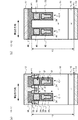
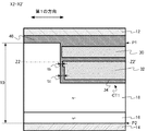
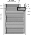
図1は、本実施形態の半導体装置の模式平面図である。図2は、本実施形態の半導体装置の一部の模式平面図である。図2は、図1の枠線Aで囲った部分の模式平面図である。図3は、本実施形態の半導体装置の一部の模式断面図である。図3(a)は、図2のY1−Y1’断面、図3(b)は図2のY2−Y2’断面である。図4は、本実施形態の半導体装置の一部の模式断面図である。図4は、図2のX1−X1’断面である。 FIG. 1 is a schematic plan view of the semiconductor device of the present embodiment. FIG. 2 is a schematic plan view of a part of the semiconductor device of the present embodiment. FIG. 2 is a schematic plan view of a portion surrounded by the frame line A in FIG. FIG. 3 is a schematic cross-sectional view of a part of the semiconductor device of the present embodiment. FIG. 3A is a cross section of Y1-Y1'in FIG. 2, and FIG. 3B is a cross section of Y2-Y2' in FIG. FIG. 4 is a schematic cross-sectional view of a part of the semiconductor device of the present embodiment. FIG. 4 is a cross section of X1-X1'of FIG.
本実施形態の半導体装置は、半導体層に形成されたトレンチの中にゲート電極を備える縦型のトレンチゲート構造の縦型MOSFETである。本実施形態の縦型MOSFETは、トレンチフィールドプレート構造を備える。本実施形態の縦型MOSFETは、電子をキャリアとするnチャネル型トランジスタである。 The semiconductor device of this embodiment is a vertical MOSFET having a vertical trench gate structure in which a gate electrode is provided in a trench formed in a semiconductor layer. The vertical MOSFET of this embodiment includes a trench field plate structure. The vertical MOSFET of this embodiment is an n-channel transistor having electrons as carriers.
本実施形態の縦型MOSFETは、半導体層10、セルトレンチCT1(第1のトレンチ)、終端トレンチTT1(第2のトレンチ)、ソース電極12(第1の電極)、ドレイン電極14(第2の電極)、ドレイン領域16、ドリフト領域18(第2の半導体領域)、ベース領域20(第1の半導体領域)、ソース領域22(第3の半導体領域)、ベースコンタクト領域24、セルゲート電極30(第1のゲート電極)、セルフィールドプレート電極32(第1のフィールドプレート電極)、セルトレンチ絶縁層34(第1の絶縁層)、終端ゲート電極40(第2のゲート電極)、終端フィールドプレート電極42(第2のフィールドプレート電極)、終端トレンチ絶縁層44(第2の絶縁層)、層間絶縁層46を備える。セルトレンチ絶縁層34(第1の絶縁層)は、ゲート絶縁膜34a(第1の部分)、上部フィールドプレート絶縁膜34b(第2の部分)、下部フィールドプレート絶縁膜34c(第3の部分)を有する。また、本実施形態の縦型MOSFETは、ゲートパッド電極50を有する。
The vertical MOSFET of this embodiment includes a
図1は、複数のセルトレンチCT1、終端トレンチTT1、ベース領域20、及び、ゲートパッド電極50のレイアウトを模式的に示している。セルトレンチCT1、及び、終端トレンチTT1は、半導体層10の中に設けられる。
FIG. 1 schematically shows the layout of a plurality of cell trenches CT1, a terminal trench TT1, a
半導体層10は、第1の面P1(以下、表面とも称する)と、第1の面P1に対向する第2の面P2(以下裏面とも称する)とを有する。半導体層10は、例えば、単結晶シリコンである。例えば、単結晶シリコンである。半導体層10の膜厚は、例えば、50μm以上300μm以下である。
The
複数のセルトレンチCT1は、第1の方向に伸長する。第1の方向は半導体層10の表面に略平行である。複数のセルトレンチCT1は、第1の方向に直交する第2の方向に略一定の間隔で配列している。
The plurality of cell trenches CT1 extend in the first direction. The first direction is substantially parallel to the surface of the
終端トレンチTT1は、複数のセルトレンチCT1を囲む。複数のセルトレンチCT1は終端トレンチTT1の内側に設けられる。終端トレンチTT1とセルトレンチCT1は、所定の距離だけ離間して設けられる。 The terminal trench TT1 surrounds a plurality of cell trenches CT1. The plurality of cell trenches CT1 are provided inside the terminal trench TT1. The terminal trench TT1 and the cell trench CT1 are provided apart by a predetermined distance.
複数のセルトレンチCT1と終端トレンチTT1は、例えば、ドライエッチング技術により半導体層10に同時に形成される。
The plurality of cell trenches CT1 and the terminal trench TT1 are simultaneously formed on the
ゲートパッド電極50は、終端トレンチTT1の外側に設けられる。
The
ソース電極12の少なくとも一部は半導体層10の第1の面P1に接する。ソース電極12は、例えば、金属である。ソース電極12には、ソース電圧が印加される。ソース電圧は、例えば、0Vである。
At least a part of the
ドレイン電極14の少なくとも一部は半導体層10の第2の面P2に接する。ドレイン電極14は、例えば、金属である。ドレイン電極14には、ドレイン電圧が印加される。ドレイン電圧は、例えば、200V以上1500V以下である。
At least a part of the
セルゲート電極30は、複数のセルトレンチCT1の、それぞれの中に設けられる。セルゲート電極30は、例えば、n型不純物又はp型不純物を含む多結晶シリコンである。
The
セルゲート電極30には、ゲート電圧が印加される。ゲート電圧を変化させることにより、縦型MOSFET100のオン・オフ動作が実現する。
A gate voltage is applied to the
セルフィールドプレート電極32は、複数のセルトレンチCT1の、それぞれの中に設けられる。セルフィールドプレート電極32は、セルゲート電極30と半導体層10の裏面との間に設けられる。セルフィールドプレート電極32は、例えば、n型不純物又はp型不純物を含む多結晶シリコンである。
The cell
セルフィールドプレート電極32の上部の第2の方向の幅は、セルフィールドプレート電極32の下部の第2の方向の幅よりも広い。本実施形態の縦型MOSFETは、セルフィールドプレート電極32の幅が深さ方向に2段階に変化する、いわゆる2段フィールドプレート構造を備える。
The width of the upper part of the cell
セルフィールドプレート電極32には、例えば、ソース電圧が印加される。セルフィールドプレート電極32にゲート電圧を印加する構成とすることも可能である。
For example, a source voltage is applied to the cell
セルゲート電極30及びセルフィールドプレート電極32は、セルトレンチ絶縁層34で囲まれる。セルトレンチ絶縁層34は、ゲート絶縁膜34a、上部フィールドプレート絶縁膜34b、下部フィールドプレート絶縁膜34cを有する。セルトレンチ絶縁層34は、例えば、酸化シリコンである。ゲート絶縁膜34a、上部フィールドプレート絶縁膜34b、及び、下部フィールドプレート絶縁膜34cは、同一の工程で形成されても、それぞれ、或いは、一部が別工程で形成されても構わない。
The
ゲート絶縁膜34aは、セルゲート電極30と半導体層10との間に位置する。ゲート絶縁膜34aは、第1の膜厚t1を有する。
The
上部フィールドプレート絶縁膜34bは、セルフィールドプレート電極32の上部と半導体層10との間に位置する。上部フィールドプレート絶縁膜34bは、第2の膜厚t2を有する。
The upper field
下部フィールドプレート絶縁膜34cは、セルフィールドプレート電極32の下部と半導体層10との間に位置する。下部フィールドプレート絶縁膜34cは、上部フィールドプレート絶縁膜34bと半導体層10の裏面との間に位置する。下部フィールドプレート絶縁膜34cは、第3の膜厚t3を有する。
The lower field
上部フィールドプレート絶縁膜34bの第2の膜厚t2は、ゲート絶縁膜34aの第1の膜厚t1よりも厚い。下部フィールドプレート絶縁膜34cの第3の膜厚t3は、上部フィールドプレート絶縁膜34bの第2の膜厚t2よりも厚い。
The second film thickness t2 of the upper field
例えば、セルトレンチCT1の内面に絶縁膜を形成した後、下部フィールドプレート絶縁膜34cに相当する部分を、マスク材で覆って絶縁膜をエッチングして薄くすることで上部フィールドプレート絶縁膜34bの形成が可能である。マスク材には、例えば、多結晶シリコンやフォトレジストを適用することが可能である。
For example, after forming an insulating film on the inner surface of the cell trench CT1, the upper field
上部フィールドプレート絶縁膜34bの第2の膜厚t2は、例えば、下部フィールドプレート絶縁膜34cの第3の膜厚t3の40%以上60%以下である。
The second film thickness t2 of the upper field
終端ゲート電極40は、終端トレンチTT1の中に設けられる。終端ゲート電極40は、例えば、n型不純物又はp型不純物を含む多結晶シリコンである。
The
終端ゲート電極40は、縦型MOSFETのオン・オフ動作には寄与しない。終端ゲート電極40には、例えば、ソース電圧が印加される。終端ゲート電極40にゲート電圧を印加する構成とすることも可能である。
The
終端フィールドプレート電極42は、終端トレンチTT1の中に設けられる。終端フィールドプレート電極42は、終端ゲート電極40と半導体層10の裏面との間に設けられる。終端フィールドプレート電極42は、例えば、n型不純物又はp型不純物を含む多結晶シリコンである。
The terminal
終端フィールドプレート電極42の上部の第2の方向の幅は、終端フィールドプレート電極42の下部の第2の方向の幅よりも広い。
The width of the upper part of the terminal
終端ゲート電極40及び終端フィールドプレート電極42は、終端トレンチ絶縁層44で囲まれる。終端トレンチ絶縁層44は、例えば、酸化シリコンである。終端フィールドプレート電極42と半導体層10との間の終端トレンチ絶縁層44には、膜厚の薄い部分(第4の部分)と、膜厚の薄い部分よりも深い位置に存在する膜厚の厚い部分(第5の部分)とがある。膜厚の薄い部分の膜厚を第4の膜厚と称し、膜厚の厚い部分の膜厚を第5の膜厚と称する。
The
ベース領域20は、半導体層10の中に設けられる。ベース領域20は、隣接する2本のセルトレンチCT1の間に位置する。ベース領域20は、p型の半導体領域である。ベース領域20のゲート絶縁膜34aに接する領域は、縦型MOSFET100のチャネル領域として機能する。ベース領域20は、ソース電極12に電気的に接続される。
The
ソース領域22は、半導体層10の中に設けられる。ソース領域22は、ベース領域20と半導体層10の表面との間に設けられる。ソース領域22は、ベース領域20とソース電極12との間に設けられる。ソース領域22は、n型の半導体領域である。ソース領域22は、ソース電極12に電気的に接続される。
The
ベースコンタクト領域24は、半導体層10の中に設けられる。ベースコンタクト領域24は、ベース領域20とソース電極12との間に設けられる。ベースコンタクト領域24は、p型の半導体領域である。ベースコンタクト領域24のp型不純物濃度は、ベース領域20のp型不純物濃度よりも高い。ベースコンタクト領域24は、ソース電極12に電気的に接続される。
The
ドリフト領域18は、半導体層10の中に設けられる。ドリフト領域18は、ベース領域20と半導体層10の裏面との間に設けられる。ドリフト領域18は、n型の半導体領域である。ドリフト領域18のn型不純物濃度は、ソース領域22のn型不純物濃度よりも低い。
The
ドレイン領域16は、半導体層10の中に設けられる。ドレイン領域16は、ドリフト領域18と半導体層10の裏面との間に設けられる。ドレイン領域16は、n型の半導体領域である。ドレイン領域16のn型不純物濃度は、ドリフト領域18のn型不純物濃度よりも高い。ドレイン領域16は、ドレイン電極14に電気的に接続される。
The
ゲートパッド電極50は、半導体層10の上に設けられる。ゲートパッド電極50は、半導体層10の表面の側に設けられる。ゲートパッド電極50は、少なくともセルゲート電極30に電気的に接続される。ゲートパッド電極50は、例えば、金属である。
The
図2は、図1の枠線Aで囲った部分の、セルトレンチCT1、終端トレンチTT1、ドレイン領域16、ドリフト領域18、ベース領域20、ソース領域22、及び、ベースコンタクト領域24の半導体層10の表面でのレイアウトを示している。
FIG. 2 shows the
図1及び図2に示すように、セルトレンチCT1の第1の方向の端部と終端トレンチTT1との間、及び、セルトレンチCT1の第1の方向の端部の近傍には、ベース領域20が存在しない。
As shown in FIGS. 1 and 2, the
例えば、セルトレンチCT1の第1の方向の端部と終端トレンチTT1との間の第1の距離(図2中のd1)は、セルトレンチCT1の中の隣接する2本のセルトレンチCT1の間の第2の距離(図2中のd2)よりも小さい。第1の距離d1は、例えば、第2の距離d2の90%以下である。 For example, the first distance (d1 in FIG. 2) between the end of the cell trench CT1 in the first direction and the terminal trench TT1 is between two adjacent cell trenches CT1 in the cell trench CT1. Is smaller than the second distance (d2 in FIG. 2). The first distance d1 is, for example, 90% or less of the second distance d2.
例えば、セルトレンチCT1の第1の方向の端部とベース領域20の第1の方向の端部との間の距離(図2中のd3)は、ベース領域20とセルトレンチCT1の半導体層10の裏面の側の端部との間の距離(図3(a)中のd4)以上である。
For example, the distance between the end of the cell trench CT1 in the first direction and the end of the
以下、本実施形態の半導体装置の作用及び効果について説明する。 Hereinafter, the operation and effect of the semiconductor device of the present embodiment will be described.
最初に、2段フィールドプレート構造の効果について説明する。図5及び図6はフィールドプレート構造の効果の説明図である。 First, the effect of the two-stage field plate structure will be described. 5 and 6 are explanatory views of the effect of the field plate structure.
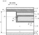
図5は、第1の比較形態の半導体装置の模式断面図及び電界分布図である。第1の比較形態の半導体装置は、縦型MOSFETである。図5は、第1の比較形態のセルトレンチCT1の断面を示す。図5の断面は、図3(a)の断面に相当する断面である。第1の比較形態の縦型MOSFETは1段フィールドプレート構造を有する。 FIG. 5 is a schematic cross-sectional view and an electric field distribution diagram of the semiconductor device of the first comparative embodiment. The semiconductor device of the first comparative form is a vertical MOSFET. FIG. 5 shows a cross section of the cell trench CT1 of the first comparative form. The cross section of FIG. 5 is a cross section corresponding to the cross section of FIG. 3 (a). The vertical MOSFET of the first comparative embodiment has a one-stage field plate structure.
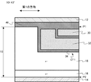
図6は、第2の比較形態半導体装置の模式断面図及び電界分布図である。第2の比較形態の半導体装置は、縦型MOSFETである。図6は、第2の比較形態のセルトレンチCT1の断面を示す。図6の断面は、図3(a)の断面に相当する断面である。第2の比較形態の縦型MOSFETは2段フィールドプレート構造を有する。 FIG. 6 is a schematic cross-sectional view and an electric field distribution diagram of the second comparative form semiconductor device. The semiconductor device of the second comparative form is a vertical MOSFET. FIG. 6 shows a cross section of the cell trench CT1 of the second comparative form. The cross section of FIG. 6 is a cross section corresponding to the cross section of FIG. 3 (a). The vertical MOSFET of the second comparative embodiment has a two-stage field plate structure.
図5に占めす1段フィールドプレート構造は、セルフィールドプレート電極32の幅が略一定であり、セルフィールドプレート電極32に段差がない。セルフィールドプレート電極32と半導体層10との間のセルトレンチ絶縁層34の膜厚が略一定である。縦型MOSFETの耐圧は、電界の深さ方向の積分値が大きくなることで向上する。1段フィールドプレート構造では、セルトレンチCT1の底部で電界のピークが生じることで、縦型MOSFETの耐圧が向上する。
In the one-stage field plate structure occupied in FIG. 5, the width of the cell
図6に示す2段フィールドプレート構造は、セルフィールドプレート電極32の上部の幅は、下部の幅よりも広い。2段フィールドプレート構造では、セルフィールドプレート電極32の幅が段階的に変化する。セルフィールドプレート電極32と半導体層10との間のセルトレンチ絶縁層34の膜厚が深さ方向に2段階に変化する。2段フィールドプレート構造では、セルトレンチCT1の底部、及び、セルフィールドプレート電極32の上部と下部の境界で電界のピークが生じる。したがって、縦型MOSFETの耐圧が1段フィールドプレート構造の場合よりも向上する。
In the two-stage field plate structure shown in FIG. 6, the width of the upper part of the cell
しかし、2段フィールドプレート構造の場合、1段フィールドプレート構造に比べ、セルトレンチCT1の端部で耐圧が低下するという問題がある。以下、説明する。 However, in the case of the two-stage field plate structure, there is a problem that the withstand voltage is lowered at the end of the cell trench CT1 as compared with the one-stage field plate structure. This will be described below.
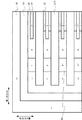
図7は第1及び第2の比較形態の模式平面図である。図8は、第1及び第2の比較形態の半導体装置の一部の模式平面図である。図8は、図7の枠線Bで囲った部分の模式平面図である。図8は、図7の枠線Bで囲った部分の、セルトレンチCT1、ドレイン領域16、ドリフト領域18、ベース領域20、ソース領域22、及び、ベースコンタクト領域24の半導体層10の表面でのレイアウトを示している。
FIG. 7 is a schematic plan view of the first and second comparative forms. FIG. 8 is a schematic plan view of a part of the semiconductor device of the first and second comparative forms. FIG. 8 is a schematic plan view of a portion surrounded by the frame line B in FIG. 7. FIG. 8 shows the cell trench CT1, the
第1及び第2の比較形態の半導体装置は、終端トレンチTT1を備えない点で第1の実施形態の縦型MOSFET100と異なっている。 The semiconductor devices of the first and second comparative embodiments are different from the vertical MOSFET 100 of the first embodiment in that they do not include the termination trench TT1.
図9は、第1の比較形態の半導体装置の一部の模式断面図である。図9は、図8のX2−X2’断面である。図9に示すようにセルトレンチCT1の第1の方向の端部で、セルフィールドプレート電極32と半導体層10との間のセルトレンチ絶縁層34の膜厚(図9中のTa)は略一定である。
FIG. 9 is a schematic cross-sectional view of a part of the semiconductor device of the first comparative embodiment. FIG. 9 is a cross section of X2-X2'of FIG. As shown in FIG. 9, the film thickness (Ta in FIG. 9) of the cell
図10は、第2の比較形態の半導体装置の一部の模式断面図である。図10は、図8のX2−X2’断面である。図10に示すようにセルトレンチCT1の第1の方向の端部で、セルフィールドプレート電極32と半導体層10との間のセルトレンチ絶縁層34の膜厚に変化がある。セルトレンチ絶縁層34の上部の膜厚(図10中のtb)は、下部の膜厚(図10中のtc)よりも薄い。
FIG. 10 is a schematic cross-sectional view of a part of the semiconductor device of the second comparative embodiment. FIG. 10 is a cross section of X2-X2'of FIG. As shown in FIG. 10, there is a change in the film thickness of the cell
図11は、第1の比較形態の半導体装置の模式平面図及び電界分布図である。図11は、図9のZ1−Z1’の第1の面に平行な断面図である。図11中の太い点線は、ドリフト領域18とベース領域20との境界の位置を示す。電界分布は図11のE1−E1’に沿った領域の電界分布である。
FIG. 11 is a schematic plan view and an electric field distribution diagram of the semiconductor device of the first comparative embodiment. FIG. 11 is a cross-sectional view parallel to the first plane of Z1-Z1'in FIG. The thick dotted line in FIG. 11 indicates the position of the boundary between the
図11に示すように、セルトレンチCT1の第1の方向の端部では、ドリフト領域18内での電界が高くなる。これは、セルトレンチCT1の端部では、2本のセルトレンチCT1の間の領域と比較して、半導体層10中の空間電荷のチャージバランスが異なり電界が集中するためである。
As shown in FIG. 11, at the end of the cell trench CT1 in the first direction, the electric field in the
図12は、第2の比較形態の半導体装置の模式平面図及び電界分布図である。図12は、図10のZ2−Z2’の第1の面に平行な断面図である。図12中の太い点線は、ドリフト領域18とベース領域20との境界の位置を示す。電界分布は図12のE2−E2’に沿った領域の電界分布である。
FIG. 12 is a schematic plan view and an electric field distribution diagram of the semiconductor device of the second comparative embodiment. FIG. 12 is a cross-sectional view parallel to the first plane of Z2-Z2'of FIG. The thick dotted line in FIG. 12 indicates the position of the boundary between the
図12に示すように、セルトレンチCT1の第1の方向の端部では、ドリフト領域18内での電界が、第1の比較形態に比べ高くなる。これは、セルトレンチ絶縁層34の上部の膜厚(図10中のtb)が、第1の比較形態のセルトレンチ絶縁層34の膜厚(図11中のta)よりも薄いことに起因する。したがって、第1の比較形態よりもセルトレンチCT1の端部でのアバランシェブレークダウンが生じやすくなり、縦型MOSFETの耐圧が低下する。
As shown in FIG. 12, at the end of the cell trench CT1 in the first direction, the electric field in the
本実施形態の縦型MOSFETでは、複数のセルトレンチCT1を囲む終端トレンチTT1を設ける。セルトレンチCT1の第1の方向の端部には、終端トレンチTT1が対向することになる。このため、図4に示すように、セルトレンチCT1の端部と終端トレンチTT1の間に、2本のセルトレンチCT1の間の領域と同様の半導体層10のメサ構造が形成される。このため、セルトレンチCT1の端部での空間電荷のチャージバランスが、2本のセルトレンチCT1の間の領域と同様に保たれることになる。したがって、セルトレンチCT1の端部での電界の集中が抑制される。よって、2段フィールドプレート構造を有する場合でも、セルトレンチCT1の端部に起因する耐圧の低下が生じない。
In the vertical MOSFET of the present embodiment, the terminal trench TT1 surrounding the plurality of cell trenches CT1 is provided. The terminal trench TT1 faces the end of the cell trench CT1 in the first direction. Therefore, as shown in FIG. 4, a mesa structure of the
本実施形態の縦型MOSFETでは、セルトレンチCT1の第1の方向の端部と終端トレンチTT1との間の第1の距離(図2中のd1)は、セルトレンチCT1の中の隣接する2本のセルトレンチCT1の間の第2の距離(図2中のd2)よりも小さいことが好ましい。上記条件を充足することにより、セルトレンチCT1の端部での空間電荷のチャージバランスが、2本のセルトレンチCT1の間の領域の空間電荷のチャージバランスに更に近づくことになり、セルトレンチCT1の端部での電界の集中が更に抑制される。 In the vertical MOSFET of the present embodiment, the first distance (d1 in FIG. 2) between the end of the cell trench CT1 in the first direction and the terminal trench TT1 is 2 adjacent to each other in the cell trench CT1. It is preferably smaller than the second distance between the book cell trench CT1 (d2 in FIG. 2). By satisfying the above conditions, the charge balance of the space charge at the end of the cell trench CT1 becomes closer to the charge balance of the space charge in the region between the two cell trenches CT1, and the cell trench CT1 The concentration of electric field at the ends is further suppressed.
セルトレンチCT1の端部での電界の集中を更に抑制する観点から、第1の距離d1は、第2の距離d2の90%以下であることがより好ましい。 From the viewpoint of further suppressing the concentration of the electric field at the end of the cell trench CT1, the first distance d1 is more preferably 90% or less of the second distance d2.
セルトレンチCT1の第1の方向の端部とベース領域20の第1の方向の端部との間の距離(図2中のd3)は、ベース領域20とセルトレンチCT1の半導体層10の裏面の側の端部との間の距離(図3(a)中のd4)以上であることが望ましい。上記条件を充足することにより、セルトレンチCT1の端部とベース領域20までの第1の方向の距離がベース領域20とセルトレンチCT1の底部までの距離以上になる。このため、セルトレンチCT1の端部とベース領域20までの第1の方向の領域の間の横方向の電界が緩和され、縦型MOSFETの耐圧が向上する。
The distance between the end of the cell trench CT1 in the first direction and the end of the
図13は、本実施形態の変形例の半導体装置の一部の模式断面図である。図13(a)、13(b)、13(c)のそれぞれは、図3(a)に対応する断面図である。 FIG. 13 is a schematic cross-sectional view of a part of the semiconductor device of the modified example of the present embodiment. 13 (a), 13 (b), and 13 (c) are cross-sectional views corresponding to FIG. 3 (a).
図13(a)は、セルフィールドプレート電極32の幅が深さ方向に3段階に変化する構造、言い換えれば、セルフィールドプレート電極32と半導体層との間のセルトレンチ絶縁層34の膜厚が深さ方向に3段階に変化する構造、すなわち、3段フィールドプレート構造である点で本実施形態と異なる。4段階以上に変化する構造とすることも可能である。また、図13(b)は、セルフィールドプレート電極32の幅が深さ方向に連続的に狭くなる点で、本実施形態と異なる。いいかえれば、セルトレンチ絶縁層34の膜厚が、半導体層10の表面から裏面に向かう方向に連続的に薄くなる。また、図13(c)はセルトレンチCT1の底部、及び、セルフィールドプレート電極32の底部の曲率が大きい点で、本実施形態と異なる。
FIG. 13A shows a structure in which the width of the cell
図13(a)、13(b)、13(c)の変形例でも、本実施形態と同様、セルトレンチCT1の端部に起因する耐圧の低下が生じないという効果が得られる。 Also in the modified examples of FIGS. 13 (a), 13 (b), and 13 (c), the effect that the withstand voltage does not decrease due to the end portion of the cell trench CT1 can be obtained as in the present embodiment.
以上、本実施形態の縦型MOSFETによれば、複数のセルトレンチCT1を囲む終端トレンチTT1を設けることで、セルトレンチCT1の端部の耐圧が向上する。したがって、トレンチフィールドプレート構造を有する縦型トランジスタの耐圧の向上が可能となる。 As described above, according to the vertical MOSFET of the present embodiment, the withstand voltage of the end portion of the cell trench CT1 is improved by providing the terminal trench TT1 surrounding the plurality of cell trench CT1s. Therefore, it is possible to improve the withstand voltage of the vertical transistor having a trench field plate structure.
(第2の実施形態)
本実施形態の半導体装置は、複数の第1のトレンチの、それぞれの第1の方向の端部とゲート電極との間に、フィールドプレート電極が位置する点で、第1の実施形態と異なっている。以下、第1の実施形態と重複する内容については記述を省略する。
(Second Embodiment)
The semiconductor device of the present embodiment differs from the first embodiment in that the field plate electrode is located between the end of each of the plurality of first trenches in the first direction and the gate electrode. There is. Hereinafter, the description of the content overlapping with the first embodiment will be omitted.
図14は、本実施形態の半導体装置の一部の模式断面図である。図14は、第1の実施形態の図4に相当する断面である。 FIG. 14 is a schematic cross-sectional view of a part of the semiconductor device of the present embodiment. FIG. 14 is a cross section corresponding to FIG. 4 of the first embodiment.
本実施形態の縦型MOSFETでは、セルトレンチCT1の第1の方向の端部とセルゲート電極30との間にセルフィールドプレート電極32が存在する。また、終端トレンチTT1には、終端ゲート電極は存在しない。
In the vertical MOSFET of the present embodiment, the cell
例えば、セルトレンチCT1中のセルフィールドプレート電極32をエッチバックプロセスにより形成する際に、セルトレンチCT1の端部と終端トレンチTT1の上をマスク材で覆うことにより、本実施形態の構造を形成することが可能である。
For example, when the cell
セルトレンチCT1の第1の方向の端部で、セルゲート電極30がセルトレンチ絶縁層34を介して半導体層10に対向する領域がない。したがって、縦型MOSFETのゲートとドレイン間の寄生容量が低減する。したがって、縦型MOSFETのスイッチング速度が上昇する。
At the end of the cell trench CT1 in the first direction, there is no region where the
また、終端トレンチTT1に終端ゲート電極が存在する場合、終端ゲート電極がゲート電圧に接続されると、ゲートとドレイン間の寄生容量が増大し、縦型MOSFETのスイッチング速度が低下する。本実施形態では、終端トレンチTT1には、終端ゲート電極が存在しないため、スイッチング速度の低下が抑制される。 Further, when the terminal gate electrode is present in the terminal trench TT1, when the terminal gate electrode is connected to the gate voltage, the parasitic capacitance between the gate and the drain increases, and the switching speed of the vertical MOSFET decreases. In the present embodiment, since the terminal gate electrode does not exist in the terminal trench TT1, the decrease in switching speed is suppressed.
以上、本実施形態の縦型MOSFETによれば、第1の実施形態と同様、縦型トランジスタの耐圧の向上が可能となる。さらに、縦型トランジスタのスイッチング速度の向上が可能となる。 As described above, according to the vertical MOSFET of the present embodiment, it is possible to improve the withstand voltage of the vertical transistor as in the first embodiment. Further, the switching speed of the vertical transistor can be improved.
(第3の実施形態)
本実施形態の半導体装置は、第2の半導体領域と第1の半導体領域の第1の方向の端部との間に、第1の半導体領域に接し、第1の半導体領域よりも第1導電型の不純物濃度の低い第1導電型の第4の半導体領域が位置する点で、第1の実施形態と異なっている。以下、第1の実施形態と重複する内容については記述を省略する。
(Third Embodiment)
The semiconductor device of the present embodiment is in contact with the first semiconductor region between the second semiconductor region and the end of the first semiconductor region in the first direction, and has a first conductivity rather than the first semiconductor region. It differs from the first embodiment in that the fourth semiconductor region of the first conductive type having a low impurity concentration of the mold is located. Hereinafter, the description of the content overlapping with the first embodiment will be omitted.
図15は、本実施形態の半導体装置の一部の模式平面図である。図15は、第1の実施形態の図2に相当する模式平面図である。 FIG. 15 is a schematic plan view of a part of the semiconductor device of the present embodiment. FIG. 15 is a schematic plan view corresponding to FIG. 2 of the first embodiment.
終端トレンチTT1と、ベース領域20との間に、リサーフ領域52(第4の半導体領域)が設けられる。ドリフト領域18と、ベース領域20との間に、リサーフ領域52が設けられる。リサーフ領域52は、ドリフト領域18とベース領域20に接する。
A resurf region 52 (fourth semiconductor region) is provided between the terminal trench TT1 and the
リサーフ領域52は、p型の半導体領域である。リサーフ領域52のp型不純物濃度は、ベース領域20のp型不純物濃度よりも低い。リサーフ領域52の深さは、ベース領域20より深くすることも、浅くすることも可能である。
The
リサーフ領域52を設けることにより、セルトレンチCT1の端部とベース領域20までの第1の方向の領域の間の横方向の電界が緩和され、縦型MOSFETの耐圧が向上する。
By providing the
以上、本実施形態の縦型MOSFETによれば、第1の実施形態よりも、更に、縦型トランジスタの耐圧が向上する。 As described above, according to the vertical MOSFET of the present embodiment, the withstand voltage of the vertical transistor is further improved as compared with the first embodiment.
(第4の実施形態)
本実施形態の半導体装置は、複数の第1のトレンチと第1の方向の端部と第2のトレンチとの間に、第1の半導体領域が位置する点で、第1の実施形態と異なっている。以下、第1の実施形態と重複する内容については記述を省略する。
(Fourth Embodiment)
The semiconductor device of the present embodiment is different from the first embodiment in that the first semiconductor region is located between the plurality of first trenches, the end portion in the first direction, and the second trench. ing. Hereinafter, the description of the content overlapping with the first embodiment will be omitted.
図16は、本実施形態の半導体装置の一部の模式平面図である。図16は、第1の実施形態の図2に相当する模式平面図である。 FIG. 16 is a schematic plan view of a part of the semiconductor device of the present embodiment. FIG. 16 is a schematic plan view corresponding to FIG. 2 of the first embodiment.
複数のセルトレンチCT1の第1の方向の端部と終端トレンチTT1との間に、ベース領域20が位置する。2本のセルトレンチCT1の端部の間に、ベース領域20が位置する。ソース領域22の第1の方向の端部と終端トレンチTT1との間の半導体層10の表面は、全てベース領域20が設けられる。
The
ソース領域22の第1の方向の端部と終端トレンチTT1との間の半導体層10の表面を、全てベース領域20とすることで、セルトレンチCT1の端部近傍で横方向に伸びる空乏層が生じなくなる。したがって、縦型MOSFETの耐圧設計が容易となる。
By setting all the surfaces of the
以上、本実施形態の縦型MOSFETによれば、第1の実施形態と同様、縦型トランジスタの耐圧の向上が可能となる。さらに、縦型トランジスタの耐圧設計が容易となる。 As described above, according to the vertical MOSFET of the present embodiment, it is possible to improve the withstand voltage of the vertical transistor as in the first embodiment. Further, the withstand voltage design of the vertical transistor becomes easy.
(第5の実施形態)
本実施形態の半導体装置は、半導体層の中に設けられ、第1の方向に伸長し、複数の第1のトレンチよりも第1の方向の長さの短い複数の第3のトレンチと、半導体層の中に設けられ、複数の第3のトレンチを囲む第4のトレンチと、を更に備える点で、第1の実施形態と異なっている。以下、第1の実施形態と重複する内容については記述を省略する。
(Fifth Embodiment)
The semiconductor device of the present embodiment includes a plurality of third trenches provided in the semiconductor layer, extending in the first direction, and having a shorter length in the first direction than the plurality of first trenches, and a semiconductor. It differs from the first embodiment in that it further comprises a fourth trench provided in the layer and surrounding the plurality of third trenches. Hereinafter, the description of the content overlapping with the first embodiment will be omitted.
図17は、本実施形態の半導体装置の模式平面図である。図17は、第1の実施形態の図1に相当する模式平面図である。図18は、本実施形態の半導体装置の一部の模式平面図である。図18は、図17の枠線Cで囲った部分の模式平面図である。図18は、第1の実施形態の図2に相当する模式平面図である。 FIG. 17 is a schematic plan view of the semiconductor device of this embodiment. FIG. 17 is a schematic plan view corresponding to FIG. 1 of the first embodiment. FIG. 18 is a schematic plan view of a part of the semiconductor device of the present embodiment. FIG. 18 is a schematic plan view of a portion surrounded by the frame line C in FIG. FIG. 18 is a schematic plan view corresponding to FIG. 2 of the first embodiment.
本実施形態の縦型MOSFETは、半導体層10、第1のセルトレンチCT1(第1のトレンチ)、第1の終端トレンチTT1(第2のトレンチ)、第2のセルトレンチCT2(第3のトレンチ)、第2の終端トレンチTT2(第4のトレンチ)を備える。
The vertical MOSFET of this embodiment includes a
複数の第1のセルトレンチCT1は、第1の方向に伸長する。第1の方向は半導体層10の表面(第1の面)に略平行である。複数の第1のセルトレンチCT1は、第2の方向に略一定の間隔で配列している。
The plurality of first cell trenches CT1 extend in the first direction. The first direction is substantially parallel to the surface (first surface) of the
第1の終端トレンチTT1は、複数の第1のセルトレンチCT1を囲む。複数の第1のセルトレンチCT1は第1の終端トレンチTT1の内側に設けられる。第1の終端トレンチTT1と第1のセルトレンチCT1は、所定の距離だけ離間して設けられる。 The first termination trench TT1 surrounds a plurality of first cell trenches CT1. The plurality of first cell trenches CT1 are provided inside the first terminal trench TT1. The first terminal trench TT1 and the first cell trench CT1 are provided apart by a predetermined distance.
複数の第2のセルトレンチCT2は、第1の方向に伸長する。第1の方向は半導体層10の表面(第1の面)に略平行である。複数の第2のセルトレンチCT2は、第2の方向に略一定の間隔で配列している。第2のセルトレンチCT2の第1の方向の長さは、第1のセルトレンチCT1の第1の方向の長さよりも短い。
The plurality of second cell trenches CT2 extend in the first direction. The first direction is substantially parallel to the surface (first surface) of the
第2の終端トレンチTT2は、複数の第2のセルトレンチCT2を囲む。複数の第2のセルトレンチCT2は第2の終端トレンチTT2の内側に設けられる。第2の終端トレンチTT2と第2のセルトレンチCT2は、所定の距離だけ離間して設けられる。 The second termination trench TT2 surrounds the plurality of second cell trenches CT2. The plurality of second cell trenches CT2 are provided inside the second terminal trench TT2. The second terminal trench TT2 and the second cell trench CT2 are provided apart by a predetermined distance.
本実施形態によれば、第1のセルトレンチCT1に加え、第2のセルトレンチCT2を設けることで、縦型MOSFETの集積度が向上する。したがって、縦型MOSFETのオン電流が増大する。 According to the present embodiment, by providing the second cell trench CT2 in addition to the first cell trench CT1, the degree of integration of the vertical MOSFET is improved. Therefore, the on-current of the vertical MOSFET increases.
複数の第1のセルトレンチCT1の中の隣接する2本の第1のセルトレンチCT1の間の距離(図18中のd2)と、第1の終端トレンチTT1と第2の終端トレンチTT2との間の距離(図18中のd5)が略同一であることが好ましい。上記条件を充足することで、トレンチの加工精度が向上する。また、半導体層10の表面の余剰領域が減り、縦型MOSFETの集積度が向上する。
The distance between two adjacent first cell trenches CT1 in the plurality of first cell trenches CT1 (d2 in FIG. 18) and the first termination trench TT1 and the second termination trench TT2. It is preferable that the distance between them (d5 in FIG. 18) is substantially the same. By satisfying the above conditions, the machining accuracy of the trench is improved. Further, the surplus region on the surface of the
以上、本実施形態の縦型MOSFETによれば、第1の実施形態と同様、縦型トランジスタの耐圧の向上が可能となる。さらに、縦型トランジスタの集積度が向上し、オン電流が増大する。 As described above, according to the vertical MOSFET of the present embodiment, it is possible to improve the withstand voltage of the vertical transistor as in the first embodiment. Further, the degree of integration of the vertical transistor is improved, and the on-current is increased.
(第6の実施形態)
本実施形態の半導体装置は、半導体層の中に設けられ、第1の方向に伸長し、複数の第1のトレンチよりも第1の方向の長さの短い複数の第3のトレンチと、半導体層の中に設けられ、第1の方向に伸長し、複数の第1のトレンチと複数の第3のトレンチとの間に位置する第4のトレンチを、更に備え、第2のトレンチが、複数の第1のトレンチ、複数の第3のトレンチ、及び、第4のトレンチを囲み、第4のトレンチの第1の方向の端部と第2のトレンチとの間の距離が、複数の第1のトレンチの、それぞれの第1の方向の端部と第2のトレンチとの間の距離、及び、複数の第3のトレンチの、それぞれの第1の方向の端部と第2のトレンチとの間の距離よりも小さい点で、第1の実施形態と異なっている。以下、第1の実施形態と重複する内容については記述を省略する。
(Sixth Embodiment)
The semiconductor device of the present embodiment is provided in a semiconductor layer, extends in a first direction, has a plurality of third trenches having a shorter length in the first direction than the plurality of first trenches, and a semiconductor. A fourth trench provided in the layer, extending in the first direction, and located between the plurality of first trenches and the plurality of third trenches is further provided, and a plurality of second trenches are provided. The distance between the first trench, the plurality of third trenches, and the fourth trench, and the distance between the end of the fourth trench in the first direction and the second trench is the plurality of first trenches. The distance between the end of each of the first directions and the second trench of the trench, and the distance between the end of each of the first directions and the second trench of the plurality of third trenches. It differs from the first embodiment in that it is smaller than the distance between them. Hereinafter, the description of the content overlapping with the first embodiment will be omitted.
図19は、本実施形態の半導体装置の模式平面図である。図19は、第1の実施形態の図1に相当する模式平面図である。図20は、本実施形態の半導体装置の一部の模式平面図である。図20は、図19の枠線Dで囲った部分の模式平面図である。図19は、第1の実施形態の図2に相当する模式平面図である。 FIG. 19 is a schematic plan view of the semiconductor device of this embodiment. FIG. 19 is a schematic plan view corresponding to FIG. 1 of the first embodiment. FIG. 20 is a schematic plan view of a part of the semiconductor device of the present embodiment. FIG. 20 is a schematic plan view of a portion surrounded by the frame line D in FIG. FIG. 19 is a schematic plan view corresponding to FIG. 2 of the first embodiment.
本実施形態の縦型MOSFETは、半導体層10、第1のセルトレンチCT1(第1のトレンチ)、終端トレンチTT1(第2のトレンチ)、第2のセルトレンチCT2(第3のトレンチ)、第3のセルトレンチCT3(第4のトレンチ)を備える。
The vertical MOSFET of the present embodiment includes a
複数の第1のセルトレンチCT1は、第1の方向に伸長する。第1の方向は半導体層10の表面(第1の面)に略平行である。複数の第1のセルトレンチCT1は、第2の方向に略一定の間隔で配列している。
The plurality of first cell trenches CT1 extend in the first direction. The first direction is substantially parallel to the surface (first surface) of the
複数の第2のセルトレンチCT2は、第1の方向に伸長する。第1の方向は半導体層10の表面(第1の面)に略平行である。複数の第2のセルトレンチCT2は、第2の方向に略一定の間隔で配列している。第2のセルトレンチCT2の第1の方向の長さは、第1のセルトレンチCT1の第1の方向の長さよりも短い。
The plurality of second cell trenches CT2 extend in the first direction. The first direction is substantially parallel to the surface (first surface) of the
第3のセルトレンチCT3は、第1の方向に伸長する。第1の方向は半導体層10の表面(第1の面)に略平行である。第3のセルトレンチCT3は、第1のセルトレンチCT1と第2のセルトレンチCT2との間に位置する。第3のセルトレンチCT3の第1の方向の長さは、第1のセルトレンチCT1の第1の方向の長さよりも短い。また、第3のセルトレンチCT3の第1の方向の長さは、第2のセルトレンチCT2の第1の方向の長さよりも長い。
The third cell trench CT3 extends in the first direction. The first direction is substantially parallel to the surface (first surface) of the
終端トレンチTT1は、複数の第1のセルトレンチCT1、複数の第2のセルトレンチCT2、及び、第3のセルトレンチCT3を囲む。 The terminal trench TT1 surrounds a plurality of first cell trenches CT1, a plurality of second cell trenches CT2, and a third cell trench CT3.
本実施形態によれば、第1のセルトレンチCT1に加え、第2のセルトレンチCT2を設けることで、縦型MOSFETの集積度が向上する。したがって、縦型MOSFETのオン電流が増大する。 According to the present embodiment, by providing the second cell trench CT2 in addition to the first cell trench CT1, the degree of integration of the vertical MOSFET is improved. Therefore, the on-current of the vertical MOSFET increases.
第3のセルトレンチCT3の第1の方向の端部と終端トレンチTT1との間の距離(図20中のd6)は、第1のセルトレンチCT1の第1の方向の端部と終端トレンチTT1との間の距離(図20中のd7)、及び、第2のセルトレンチCT2の第1の方向の端部と終端トレンチTT1との間の距離(図20中のd8)よりも小さい。第1のセルトレンチCT1の第1の方向の端部と終端トレンチTT1との間の距離(図20中のd7)、及び、第2のセルトレンチCT2の第1の方向の端部と終端トレンチTT1との間の距離(図20中のd8)は、例えば、略同一である。 The distance between the end of the third cell trench CT3 in the first direction and the end trench TT1 (d6 in FIG. 20) is the distance between the end of the first cell trench CT1 in the first direction and the end trench TT1. It is smaller than the distance between (d7 in FIG. 20) and the distance between the end of the second cell trench CT2 in the first direction and the terminal trench TT1 (d8 in FIG. 20). The distance between the end of the first cell trench CT1 in the first direction and the end trench TT1 (d7 in FIG. 20), and the end of the second cell trench CT2 in the first direction and the end trench. The distance to TT1 (d8 in FIG. 20) is, for example, substantially the same.
第3のセルトレンチCT3の端部は、終端トレンチTT1が屈曲する特異点に存在する。第3のセルトレンチCT3の第1の方向の端部と終端トレンチTT1との間の距離(図20中のd6)を短くすることにより、空間電荷とのチャージバランスが調整され、第3のセルトレンチCT3の端部での電界集中が抑制される。したがって、縦型MOSFETの耐圧の低下が抑制される。 The end of the third cell trench CT3 is located at a singular point where the termination trench TT1 bends. By shortening the distance between the end of the third cell trench CT3 in the first direction and the end trench TT1 (d6 in FIG. 20), the charge balance with the space charge is adjusted, and the third cell The electric field concentration at the end of the trench CT3 is suppressed. Therefore, the decrease in withstand voltage of the vertical MOSFET is suppressed.
以上、本実施形態の縦型MOSFETによれば、第1の実施形態と同様、縦型トランジスタの耐圧の向上が可能となる。さらに、縦型トランジスタの集積度が向上し、オン電流が増大する。 As described above, according to the vertical MOSFET of the present embodiment, it is possible to improve the withstand voltage of the vertical transistor as in the first embodiment. Further, the degree of integration of the vertical transistor is improved, and the on-current is increased.
(第7の実施形態)
本実施形態の半導体装置は、複数の第1のトレンチの一部の中の隣接する2本の第1のトレンチの間の第1の半導体領域の第1の方向の長さが、複数の第1のトレンチの残部の中の隣接する2本の第1のトレンチの間の第1の半導体領域の第1の方向の長さよりも短い点で、第1の実施形態と異なっている。以下、第1の実施形態と重複する内容については記述を省略する。
(7th Embodiment)
In the semiconductor device of the present embodiment, the length of the first semiconductor region between two adjacent first trenches in a part of the plurality of first trenches is a plurality of first semiconductor regions. It differs from the first embodiment in that it is shorter than the length of the first semiconductor region between the two adjacent first trenches in the rest of one trench in the first direction. Hereinafter, the description of the content overlapping with the first embodiment will be omitted.
図21は、本実施形態の半導体装置の模式平面図である。図21は、第1の実施形態の図1に相当する模式平面図である。 FIG. 21 is a schematic plan view of the semiconductor device of this embodiment. FIG. 21 is a schematic plan view corresponding to FIG. 1 of the first embodiment.
複数の第1のセルトレンチCT1の一部は、ゲートパッド電極50の下にも設けられる。ゲートパッド電極50の下に設けられた複数の第1のセルトレンチCT1の一部の中の隣接する2本の第1のセルトレンチCT1の間のベース領域20の第1の方向の長さは、複数の第1のセルトレンチCT1の残部の中の隣接する2本の間のベース領域20の第1の方向の長さよりも短い。ゲートパッド電極50の下の領域には、ベース領域20が設けられない。
A part of the plurality of first cell trenches CT1 is also provided under the
本実施形態によれば、第1のセルトレンチCT1の本数が増えることで、縦型MOSFETの集積度が向上する。したがって、縦型MOSFETのオン電流が増大する。 According to the present embodiment, the degree of integration of the vertical MOSFET is improved by increasing the number of the first cell trench CT1s. Therefore, the on-current of the vertical MOSFET increases.
また、ベース領域20へのコンタクトを設けることが困難なゲートパッド電極50の下の領域から、ベース領域20を除くことで、ホールの引き抜き効率の低下を防止する。したがって、縦型MOSFETのアバランシェ耐量の低下が抑制される。
Further, by removing the
以上、本実施形態の縦型MOSFETによれば、第1の実施形態と同様、縦型トランジスタの耐圧の向上が可能となる。さらに、縦型トランジスタの集積度が向上し、オン電流が増大する。 As described above, according to the vertical MOSFET of the present embodiment, it is possible to improve the withstand voltage of the vertical transistor as in the first embodiment. Further, the degree of integration of the vertical transistor is improved, and the on-current is increased.
(第8の実施形態)
本実施形態の半導体装置は、第1の面と、第1の面と対向する第2の面を有する半導体層と、第1の面に接する第1の電極と、第2の面に接する第2の電極と、半導体層の中に設けられ、第1の面に略平行な第1の方向に伸長する複数のトレンチと、複数のトレンチの、それぞれの中に設けられたゲート電極と、複数のトレンチの、それぞれの中に設けられ、ゲート電極と第2の面との間に設けられたフィールドプレート電極と、複数のトレンチの、それぞれの中に設けられ、ゲート電極と半導体層との間に位置し第1の膜厚を有する第1の部分と、フィールドプレート電極と半導体層との間に位置し第1の膜厚よりも厚い第2の膜厚を有する第2の部分と、フィールドプレート電極と半導体層との間の第2の部分と第2の面との間に位置し第2の膜厚よりも厚い第3の膜厚を有する第3の部分と、フィールドプレート電極の第1の方向の端部と半導体層との間であって第2の部分と第1の面から略同一の深さに位置し、第2の膜厚よりも厚い第4の膜厚を有する第4の部分、を有する絶縁層と、半導体層の中に設けられ、複数のトレンチの中の隣接する2本のトレンチの間に位置する第1導電型の第1の半導体領域と、半導体層の中に設けられ、第1の半導体領域と第2の面との間に位置する第2導電型の第2の半導体領域と、半導体層の中に設けられ、第1の半導体領域と第1の電極との間に位置し、第1の電極に電気的に接続された第2導電型の第3の半導体領域と、を備える。
(8th Embodiment)
The semiconductor device of the present embodiment has a first surface, a semiconductor layer having a second surface facing the first surface, a first electrode in contact with the first surface, and a second surface in contact with the second surface. A plurality of electrodes, a plurality of trenches provided in the semiconductor layer and extending in a first direction substantially parallel to the first surface, and a plurality of gate electrodes provided in each of the plurality of trenches. A field plate electrode provided in each of the trenches and provided between the gate electrode and the second surface, and a plurality of trenches provided in each of the gate electrodes and the semiconductor layer. A first portion located in the field and having a first film thickness, a second portion located between the field plate electrode and the semiconductor layer and having a second film thickness thicker than the first film thickness, and a field. A third portion located between the second portion and the second surface between the plate electrode and the semiconductor layer and having a third film thickness thicker than the second film thickness, and a third portion of the field plate electrode. A second having a fourth film thickness that is thicker than the second film thickness and is located between the end portion in the first direction and the semiconductor layer at substantially the same depth from the second portion and the first surface. An insulating layer having four portions, a first conductive type first semiconductor region provided in the semiconductor layer and located between two adjacent trenches in a plurality of trenches, and a semiconductor layer. A second conductive type second semiconductor region provided inside and located between the first semiconductor region and the second surface, and a first semiconductor region and a first semiconductor region provided in the semiconductor layer. It includes a second conductive type third semiconductor region, which is located between the electrodes and is electrically connected to the first electrode.
図22は、本実施形態の半導体装置の模式平面図である。図23は、本実施形態の半導体装置の一部の模式平面図である。図23は、図22の枠線Eで囲った部分の模式平面図である。図24は、本実施形態の半導体装置の一部の模式断面図である。図24(a)は、図23のY3−Y3’断面、図24(b)は図23のY4−Y4’断面である。図25は、本実施形態の半導体装置の一部の模式断面図である。図25は、図23のX3−X3’断面である。 FIG. 22 is a schematic plan view of the semiconductor device of this embodiment. FIG. 23 is a schematic plan view of a part of the semiconductor device of the present embodiment. FIG. 23 is a schematic plan view of a portion surrounded by the frame line E in FIG. 22. FIG. 24 is a schematic cross-sectional view of a part of the semiconductor device of the present embodiment. FIG. 24A is a cross section of Y3-Y3'in FIG. 23, and FIG. 24B is a cross section of Y4-Y4' in FIG. 23. FIG. 25 is a schematic cross-sectional view of a part of the semiconductor device of the present embodiment. FIG. 25 is a cross section of X3-X3'of FIG. 23.
本実施形態の半導体装置は、半導体層に形成されたトレンチの中にゲート電極を備える縦型のトレンチゲート構造の縦型MOSFETである。本実施形態の縦型MOSFETは、トレンチフィールドプレート構造を備える。本実施形態の縦型MOSFETは、電子をキャリアとするnチャネル型トランジスタである。 The semiconductor device of this embodiment is a vertical MOSFET having a vertical trench gate structure in which a gate electrode is provided in a trench formed in a semiconductor layer. The vertical MOSFET of this embodiment includes a trench field plate structure. The vertical MOSFET of this embodiment is an n-channel transistor having electrons as carriers.
本実施形態の縦型MOSFETは、半導体層10、セルトレンチCT1(トレンチ)、ソース電極12、ドレイン電極14、ドレイン領域16、ドリフト領域18、ベース領域20、ソース領域22、ベースコンタクト領域24、セルゲート電極30(ゲート電極)、セルフィールドプレート電極32(フィールドプレート電極)、セルトレンチ絶縁層34(絶縁層)、層間絶縁層46を備える。セルトレンチ絶縁層34(絶縁層)は、ゲート絶縁膜34a(第1の部分)、上部フィールドプレート絶縁膜34b(第2の部分)、下部フィールドプレート絶縁膜34c(第3の部分)、端部フィールドプレート絶縁膜34d(第4の部分)を有する。また、本実施形態の縦型MOSFETは、ゲートパッド電極50を有する。
The vertical MOSFET of the present embodiment includes a
図23は、複数のセルトレンチCT1、ベース領域20、及び、ゲートパッド電極50のレイアウトを模式的に示している。セルトレンチCT1は、半導体層10の中に設けられる。
FIG. 23 schematically shows the layout of the plurality of cell trenches CT1, the
半導体層10は、第1の面P1(以下、表面とも称する)と、第1の面P1に対向する第2の面P2(以下裏面とも称する)とを有する。半導体層10は、例えば、単結晶シリコンである。例えば、単結晶シリコンである。半導体層10の膜厚は、例えば、50μm以上300μm以下である。
The
複数のセルトレンチCT1は、第1の方向に伸長する。第1の方向は半導体層10の表面に略平行である。複数のセルトレンチCT1は、第1の方向に直交する第2の方向に略一定の間隔で配列している。
The plurality of cell trenches CT1 extend in the first direction. The first direction is substantially parallel to the surface of the
ゲートパッド電極50は、複数のセルトレンチCT1の外側に設けられる。
The
ソース電極12の少なくとも一部は半導体層10の第1の面P1に接する。ソース電極12は、例えば、金属である。ソース電極12には、ソース電圧が印加される。ソース電圧は、例えば、0Vである。
At least a part of the
ドレイン電極14の少なくとも一部は半導体層10の第2の面P2に接する。ドレイン電極14は、例えば、金属である。ドレイン電極14には、ドレイン電圧が印加される。ドレイン電圧は、例えば、200V以上1500V以下である。
At least a part of the
セルゲート電極30は、複数のセルトレンチCT1の、それぞれの中に設けられる。セルゲート電極30は、例えば、n型不純物又はp型不純物を含む多結晶シリコンである。
The
セルゲート電極30には、ゲート電圧が印加される。ゲート電圧を変化させることにより、縦型MOSFET100のオン・オフ動作が実現する。
A gate voltage is applied to the
セルフィールドプレート電極32は、複数のセルトレンチCT1の、それぞれの中に設けられる。セルフィールドプレート電極32は、セルゲート電極30と半導体層10の裏面との間に設けられる。セルフィールドプレート電極32は、例えば、n型不純物又はp型不純物を含む多結晶シリコンである。
The cell
セルフィールドプレート電極32の上部の第2の方向の幅は、セルフィールドプレート電極32の下部の第2の方向の幅よりも広い。本実施形態の縦型MOSFETは、セルフィールドプレート電極32の幅が深さ方向に2段階に変化する、いわゆる2段フィールドプレート構造を備える。
The width of the upper part of the cell
セルフィールドプレート電極32には、例えば、ソース電圧が印加される。セルフィールドプレート電極32にゲート電圧を印加する構成とすることも可能である。
For example, a source voltage is applied to the cell
セルゲート電極30及びセルフィールドプレート電極32は、セルトレンチ絶縁層34で囲まれる。セルトレンチ絶縁層34は、ゲート絶縁膜34a、上部フィールドプレート絶縁膜34b、下部フィールドプレート絶縁膜34c、端部フィールドプレート絶縁膜34dを有する。セルトレンチ絶縁層34は、例えば、酸化シリコンである。ゲート絶縁膜34a、上部フィールドプレート絶縁膜34b、下部フィールドプレート絶縁膜34c、及び、端部フィールドプレート絶縁膜34dは、同一の工程で形成されても、それぞれ、或いは、一部が別工程で形成されても構わない。
The
ゲート絶縁膜34aは、セルゲート電極30と半導体層10との間に位置する。ゲート絶縁膜34aは、第1の膜厚t1を有する。
The
上部フィールドプレート絶縁膜34bは、セルフィールドプレート電極32の上部と半導体層10との間に位置する。上部フィールドプレート絶縁膜34bは、第2の膜厚t2を有する。
The upper field
下部フィールドプレート絶縁膜34cは、セルフィールドプレート電極32の下部と半導体層10との間に位置する。下部フィールドプレート絶縁膜34cは、上部フィールドプレート絶縁膜34bと半導体層10の裏面との間に位置する。下部フィールドプレート絶縁膜34cは、第3の膜厚t3を有する。
The lower field
上部フィールドプレート絶縁膜34bの第2の膜厚t2は、ゲート絶縁膜34aの第1の膜厚t1よりも厚い。下部フィールドプレート絶縁膜34cの第3の膜厚t3は、上部フィールドプレート絶縁膜34bの第2の膜厚t2よりも厚い。
The second film thickness t2 of the upper field
上部フィールドプレート絶縁膜34bの第2の膜厚t2は、例えば、下部フィールドプレート絶縁膜34cの第3の膜厚t3の40%以上60%以下である。
The second film thickness t2 of the upper field
端部フィールドプレート絶縁膜34dは、セルフィールドプレート電極32の第1の方向の端部と半導体層10との間に位置する。端部フィールドプレート絶縁膜34dは、上部フィールドプレート絶縁膜34bと、半導体層10の表面(第1の面)から略同一の深さに位置する。端部フィールドプレート絶縁膜34dの半導体層10の表面(第1の面)からの深さは、上部フィールドプレート絶縁膜34bの半導体層10の表面(第1の面)からの深さと略同一である。ここで、「深さ」とは、半導体層10の表面(第1の面)から裏面(第2の面)に向かう方向の距離である。
The end field
端部フィールドプレート絶縁膜34dの第4の膜厚t4は、上部フィールドプレート絶縁膜34bの第2の膜厚t2よりも厚い。端部フィールドプレート絶縁膜34dの第4の膜厚t4は、例えば、下部フィールドプレート絶縁膜34cの第3の膜厚t3と略同一である。
The fourth film thickness t4 of the end field
例えば、セルトレンチCT1の内面に絶縁膜を形成した後、下部フィールドプレート絶縁膜34cに相当する部分を、第1のマスク材で覆って絶縁膜をエッチングして薄くすることで上部フィールドプレート絶縁膜34bの形成が可能である。絶縁膜をエッチングする際に、セルトレンチCT1の第1の方向の端部を第2のマスク材で覆うことで、絶縁膜がエッチングされず、端部フィールドプレート絶縁膜34dの形成が可能となる。例えば、第1のマスク材には多結晶シリコン、第2のマスク材にはフォトレジストを適用することが可能である。
For example, after forming an insulating film on the inner surface of the cell trench CT1, the portion corresponding to the lower field
ベース領域20は、半導体層10の中に設けられる。ベース領域20は、隣接する2本のセルトレンチCT1の間に位置する。ベース領域20は、p型の半導体領域である。ベース領域20のゲート絶縁膜34aに接する領域は、縦型MOSFET100のチャネル領域として機能する。ベース領域20は、ソース電極12に電気的に接続される。
The
ソース領域22は、半導体層10の中に設けられる。ソース領域22は、ベース領域20と半導体層10の表面との間に設けられる。ソース領域22は、ベース領域20とソース電極12との間に設けられる。ソース領域22は、n型の半導体領域である。ソース領域22は、ソース電極12に電気的に接続される。
The
ベースコンタクト領域24は、半導体層10の中に設けられる。ベースコンタクト領域24は、ベース領域20とソース電極12との間に設けられる。ベースコンタクト領域24は、p型の半導体領域である。ベースコンタクト領域24のp型不純物濃度は、ベース領域20のp型不純物濃度よりも高い。ベースコンタクト領域24は、ソース電極12に電気的に接続される。
The
ドリフト領域18は、半導体層10の中に設けられる。ドリフト領域18は、ベース領域20と半導体層10の裏面との間に設けられる。ドリフト領域18は、n型の半導体領域である。ドリフト領域18のn型不純物濃度は、ソース領域22のn型不純物濃度よりも低い。
The
ドレイン領域16は、半導体層10の中に設けられる。ドレイン領域16は、ドリフト領域18と半導体層10の裏面との間に設けられる。ドレイン領域16は、n型の半導体領域である。ドレイン領域16のn型不純物濃度は、ドリフト領域18のn型不純物濃度よりも高い。ドレイン領域16は、ドレイン電極14に電気的に接続される。
The
ゲートパッド電極50は、半導体層10の上に設けられる。ゲートパッド電極50は、半導体層10の表面の側に設けられる。ゲートパッド電極50は、少なくともセルゲート電極30に電気的に接続される。ゲートパッド電極50は、例えば、金属である。
The
図23は、図22の枠線Eで囲った部分の、セルトレンチCT1、ドレイン領域16、ドリフト領域18、ベース領域20、ソース領域22、及び、ベースコンタクト領域24の半導体層10の表面でのレイアウトを示している。
FIG. 23 shows the cell trench CT1, the
例えば、セルトレンチCT1の第1の方向の端部とベース領域20の第1の方向の端部との間の距離(図23中のd3)は、ベース領域20とセルトレンチCT1の半導体層10の裏面の側の端部との間の距離(図24(a)中のd4)以上である。
For example, the distance between the end of the cell trench CT1 in the first direction and the end of the
以下、本実施形態の半導体装置の作用及び効果について説明する。 Hereinafter, the operation and effect of the semiconductor device of the present embodiment will be described.
最初に、2段フィールドプレート構造の効果について説明する。図5及び図6はフィールドプレート構造の効果の説明図である。 First, the effect of the two-stage field plate structure will be described. 5 and 6 are explanatory views of the effect of the field plate structure.
図5は、第1の比較形態の半導体装置の模式断面図及び電界分布図である。第1の比較形態の半導体装置は、縦型MOSFETである。図5は、第1の比較形態のセルトレンチCT1の断面を示す。図5の断面は、図3(a)の断面に相当する断面である。第1の比較形態の縦型MOSFETは1段フィールドプレート構造を有する。 FIG. 5 is a schematic cross-sectional view and an electric field distribution diagram of the semiconductor device of the first comparative embodiment. The semiconductor device of the first comparative form is a vertical MOSFET. FIG. 5 shows a cross section of the cell trench CT1 of the first comparative form. The cross section of FIG. 5 is a cross section corresponding to the cross section of FIG. 3 (a). The vertical MOSFET of the first comparative embodiment has a one-stage field plate structure.
図6は、第2の比較形態半導体装置の模式断面図及び電界分布図である。第2の比較形態の半導体装置は、縦型MOSFETである。図6は、第2の比較形態のセルトレンチCT1の断面を示す。図6の断面は、図3(a)の断面に相当する断面である。第2の比較形態の縦型MOSFETは2段フィールドプレート構造を有する。 FIG. 6 is a schematic cross-sectional view and an electric field distribution diagram of the second comparative form semiconductor device. The semiconductor device of the second comparative form is a vertical MOSFET. FIG. 6 shows a cross section of the cell trench CT1 of the second comparative form. The cross section of FIG. 6 is a cross section corresponding to the cross section of FIG. 3 (a). The vertical MOSFET of the second comparative embodiment has a two-stage field plate structure.
図5に占めす1段フィールドプレート構造は、セルフィールドプレート電極32の幅が略一定であり、セルフィールドプレート電極32に段差がない。縦型MOSFETの耐圧は、電界の深さ方向の積分値が大きくなることで向上する。1段フィールドプレート構造では、セルトレンチCT1の底部で電界のピークが生じることで、縦型MOSFETの耐圧が向上する。
In the one-stage field plate structure occupied in FIG. 5, the width of the cell
図6に占めす2段フィールドプレート構造は、セルフィールドプレート電極32の上部の幅は、下部の幅よりも広い。2段フィールドプレート構造では、セルフィールドプレート電極32の幅が段階的に変化する、2段フィールドプレート構造では、セルトレンチCT1の底部、及び、セルフィールドプレート電極32の上部と下部の境界で電界のピークが生じることで、縦型MOSFETの耐圧が1段フィールドプレート構造の場合よりも向上する。
In the two-stage field plate structure occupied in FIG. 6, the width of the upper part of the cell
しかし、2段フィールドプレート構造の場合、1段フィールドプレート構造に比べ、セルトレンチCT1の端部で耐圧が低下するという問題がある。以下、説明する。 However, in the case of the two-stage field plate structure, there is a problem that the withstand voltage is lowered at the end of the cell trench CT1 as compared with the one-stage field plate structure. This will be described below.
図7は第1及び第2の比較形態の模式平面図である。図8は、第1及び第2の比較形態の半導体装置の一部の模式平面図である。図8は、図7の枠線Bで囲った部分の模式平面図である。図8は、図7の枠線Bで囲った部分の、セルトレンチCT1、ドレイン領域16、ドリフト領域18、ベース領域20、ソース領域22、及び、ベースコンタクト領域24の半導体層10の表面でのレイアウトを示している。
FIG. 7 is a schematic plan view of the first and second comparative forms. FIG. 8 is a schematic plan view of a part of the semiconductor device of the first and second comparative forms. FIG. 8 is a schematic plan view of a portion surrounded by the frame line B in FIG. 7. FIG. 8 shows the cell trench CT1, the
第1及び第2の比較形態の半導体装置は、終端トレンチTT1を備えない点で第1の実施形態の縦型MOSFET100と異なっている。 The semiconductor devices of the first and second comparative embodiments are different from the vertical MOSFET 100 of the first embodiment in that they do not include the termination trench TT1.
図9は、第1の比較形態の半導体装置の一部の模式断面図である。図9は、図8のX2−X2’断面である。図9に示すようにセルトレンチCT1の第1の方向の端部で、セルフィールドプレート電極32と半導体層10との間のセルトレンチ絶縁層34の膜厚(図9中のTa)は略一定である。
FIG. 9 is a schematic cross-sectional view of a part of the semiconductor device of the first comparative embodiment. FIG. 9 is a cross section of X2-X2'of FIG. As shown in FIG. 9, the film thickness (Ta in FIG. 9) of the cell
図10は、第2の比較形態の半導体装置の一部の模式断面図である。図10は、図8のX2−X2’断面である。図10に示すようにセルトレンチCT1の第1の方向の端部で、セルフィールドプレート電極32と半導体層10との間のセルトレンチ絶縁層34の膜厚に変化がある。セルトレンチ絶縁層34の上部の膜厚(図10中のtb)は、下部の膜厚(図10中のtc)よりも薄い。
FIG. 10 is a schematic cross-sectional view of a part of the semiconductor device of the second comparative embodiment. FIG. 10 is a cross section of X2-X2'of FIG. As shown in FIG. 10, there is a change in the film thickness of the cell
図11は、第1の比較形態の半導体装置の模式平面図及び電界分布図である。図11は、図9のZ1−Z1’の第1の面に平行な断面図である。図11中の太い点線は、ドリフト領域18とベース領域20との境界の位置を示す。電界分布は図11のE1−E1’に沿った領域の電界分布である。
FIG. 11 is a schematic plan view and an electric field distribution diagram of the semiconductor device of the first comparative embodiment. FIG. 11 is a cross-sectional view parallel to the first plane of Z1-Z1'in FIG. The thick dotted line in FIG. 11 indicates the position of the boundary between the
図11に示すように、セルトレンチCT1の第1の方向の端部では、ドリフト領域18内での電界が高くなる。これは、セルトレンチCT1の端部では、2本のセルトレンチCT1の間の領域と比較して、半導体層10中の空間電荷のチャージバランスが異なり電界が集中するためである。
As shown in FIG. 11, at the end of the cell trench CT1 in the first direction, the electric field in the
図12は、第2の比較形態の半導体装置の模式平面図及び電界分布図である。図12は、図10のZ2−Z2’の第1の面に平行な断面図である。図12中の太い点線は、ドリフト領域18とベース領域20との境界の位置を示す。電界分布は図12のE2−E2’に沿った領域の電界分布である。
FIG. 12 is a schematic plan view and an electric field distribution diagram of the semiconductor device of the second comparative embodiment. FIG. 12 is a cross-sectional view parallel to the first plane of Z2-Z2'of FIG. The thick dotted line in FIG. 12 indicates the position of the boundary between the
図12に示すように、セルトレンチCT1の第1の方向の端部では、ドリフト領域18内での電界が、第1の比較形態に比べ高くなる。これは、セルトレンチ絶縁層34の上部の膜厚(図10中のtb)が、第1の比較形態のセルトレンチ絶縁層34の膜厚(図11中のta)よりも薄いことに起因する。したがって、第1の比較形態よりもセルトレンチCT1の端部でのアバランシェブレークダウンが生じやすくなり、縦型MOSFETの耐圧が低下する。
As shown in FIG. 12, at the end of the cell trench CT1 in the first direction, the electric field in the
図26は、本実施形態の半導体装置の模式平面図及び電界分布図である。図26は、図25のZ3−Z3’の半導体層10の表面(第1の面)に平行な断面図である。図26中の太い点線は、ドリフト領域18とベース領域20との境界の位置を示す。電界分布は図26のE3−E3’に沿った領域の電界分布である。
FIG. 26 is a schematic plan view and an electric field distribution diagram of the semiconductor device of the present embodiment. FIG. 26 is a cross-sectional view parallel to the surface (first surface) of the
本実施形態の縦型MOSFETでは、第2の比較形態に比べ、セルトレンチCT1の第1の方向の端部のセルトレンチ絶縁層34の膜厚が厚くなっている。セルトレンチCT1の第1の方向の端部のセルトレンチ絶縁層34の膜厚は、第1の方向及び第2の方向のいずれも厚くなっている。第2の方向の膜厚が厚いことにより、セルフィールドプレート電極32が第1の方向にも2段フィールドプレート構造となっている。したがって、第2の比較形態と比較して、セルトレンチCT1の端部での電界集中が緩和され、アバランシェブレークダウンが抑制される。よって、縦型MOSFETの耐圧の低下が抑制される。
In the vertical MOSFET of the present embodiment, the film thickness of the cell
セルトレンチCT1の第1の方向の端部とベース領域20の第1の方向の端部との間の距離(図23中のd3)は、ベース領域20とセルトレンチCT1の半導体層10の裏面の側の端部との間の距離(図24(a)中のd4)以上であることが望ましい。上記条件を充足することにより、セルトレンチCT1の端部とベース領域20までの第1の方向の距離がベース領域20とセルトレンチCT1の底部までの距離以上になる。このため、セルトレンチCT1の端部とベース領域20までの第1の方向の領域の間の横方向の電界が緩和され、縦型MOSFETの耐圧が向上する。
The distance between the end of the cell trench CT1 in the first direction and the end of the
(第9の実施形態)
本実施形態の半導体装置は、複数のトレンチの、それぞれの第1の方向の端部とゲート電極との間に、フィールドプレート電極が位置する点で、第8の実施形態と異なっている。以下、第8の実施形態と重複する内容については記述を省略する。
(9th Embodiment)
The semiconductor device of the present embodiment is different from the eighth embodiment in that the field plate electrode is located between the end of each of the plurality of trenches in the first direction and the gate electrode. Hereinafter, the description of the content overlapping with the eighth embodiment will be omitted.
図27は、本実施形態の半導体装置の一部の模式断面図である。図27は、第8の実施形態の図25に相当する断面である。 FIG. 27 is a schematic cross-sectional view of a part of the semiconductor device of the present embodiment. FIG. 27 is a cross section corresponding to FIG. 25 of the eighth embodiment.
本実施形態の縦型MOSFETでは、セルトレンチCT1の第1の方向の端部とセルゲート電極30との間にセルフィールドプレート電極32が存在する。
In the vertical MOSFET of the present embodiment, the cell
例えば、セルトレンチCT1中のセルフィールドプレート電極32をエッチバックプロセスにより形成する際に、セルトレンチCT1の端部と終端トレンチTT1の上をマスク材で覆うことにより、本実施形態の構造を形成することが可能である。
For example, when the cell
本実施形態の縦型MOSFETでは、セルトレンチCT1の第1の方向の端部で、セルゲート電極30がセルトレンチ絶縁層34を介して半導体層10に対向する領域がない。したがって、縦型MOSFETのゲートとドレイン間の寄生容量が低減する。したがって、縦型MOSFETのスイッチング速度が上昇する。
In the vertical MOSFET of the present embodiment, there is no region where the
以上、本実施形態の縦型MOSFETによれば、第8の実施形態と同様、縦型トランジスタの耐圧の向上が可能となる。さらに、縦型トランジスタのスイッチング速度の向上が可能となる。 As described above, according to the vertical MOSFET of the present embodiment, it is possible to improve the withstand voltage of the vertical transistor as in the eighth embodiment. Further, the switching speed of the vertical transistor can be improved.
第1ないし第9の実施形態においては、半導体層が単結晶シリコンである場合を例に説明したが、半導体層は単結晶シリコンに限られることはない。例えば、単結晶炭化珪素等、その他の単結晶半導体であっても構わない。 In the first to ninth embodiments, the case where the semiconductor layer is single crystal silicon has been described as an example, but the semiconductor layer is not limited to single crystal silicon. For example, other single crystal semiconductors such as single crystal silicon carbide may be used.
第1ないし第9の実施形態においては、第1導電型がp型、第2導電型がn型のnチャネル型トランジスタを例に説明したが、第1導電型がn型、第2導電型がp型のpチャネル型トランジスタであっても構わない。 In the first to ninth embodiments, an n-channel transistor in which the first conductive type is p-type and the second conductive type is n-type has been described as an example, but the first conductive type is n-type and the second conductive type is n-type. May be a p-type p-channel type transistor.
第1ないし第9の実施形態においては、縦型トランジスタが縦型MOSFETである場合を例に説明したが、縦型トランジスタが縦型IGBTであっても構わない。 In the first to ninth embodiments, the case where the vertical transistor is a vertical MOSFET has been described as an example, but the vertical transistor may be a vertical IGBT.
本発明のいくつかの実施形態を説明したが、これらの実施形態は、例として提示したものであり、発明の範囲を限定することは意図していない。これら新規な実施形態は、その他の様々な形態で実施されることが可能であり、発明の要旨を逸脱しない範囲で、種々の省略、置き換え、変更を行うことができる。例えば、一実施形態の構成要素を他の実施形態の構成要素と置き換え又は変更してもよい。これら実施形態やその変形は、発明の範囲や要旨に含まれるとともに、特許請求の範囲に記載された発明とその均等の範囲に含まれる。 Although some embodiments of the present invention have been described, these embodiments are presented as examples and are not intended to limit the scope of the invention. These novel embodiments can be implemented in various other embodiments, and various omissions, replacements, and changes can be made without departing from the gist of the invention. For example, the components of one embodiment may be replaced or modified with the components of another embodiment. These embodiments and modifications thereof are included in the scope and gist of the invention, and are included in the scope of the invention described in the claims and the equivalent scope thereof.
10 半導体層
12 ソース電極(第1の電極)
14 ドレイン電極(第2の電極)
16 ドレイン領域
18 ドリフト領域(第2の半導体領域)
20 ベース領域(第1の半導体領域)
22 ソース領域(第3の半導体領域)
24 ベースコンタクト領域
30 セルゲート電極(第1のゲート電極)
32 セルフィールドプレート電極(第1のフィールドプレート電極、フィールドプレート電極)
34 セルトレンチ絶縁層(第1の絶縁層、絶縁層)
34a ゲート絶縁膜(第1の部分)
34b 上部フィールドプレート絶縁膜(第2の部分)
34c 下部フィールドプレート絶縁膜(第3の部分)
34d 端部フィールドプレート絶縁膜(第4の部分)
40 終端ゲート電極(第2のゲート電極)
42 終端フィールドプレート電極(第2のフィールドプレート電極)
44 終端トレンチ絶縁層(第2の絶縁層)
46 層間絶縁層
50 ゲートパッド電極
52 リサーフ領域(第4の半導体領域)
CT1 セルトレンチ、第1のセルトレンチ(第1のトレンチ、トレンチ)
CT2 第2のセルトレンチ(第3のトレンチ)
CT3 第3のセルトレンチ(第4のトレンチ)
TT1 終端トレンチ、第1の終端トレンチ(第2のトレンチ)
TT2 第2の終端トレンチ(第4のトレンチ)
P1 第1の面
P2 第2の面
10
14 Drain electrode (second electrode)
16
20 base region (first semiconductor region)
22 Source region (third semiconductor region)
24
32 Cell field plate electrode (first field plate electrode, field plate electrode)
34 Cell trench insulation layer (first insulation layer, insulation layer)
34a Gate insulating film (first part)
34b Upper field plate insulating film (second part)
34c Lower field plate insulating film (third part)
34d End field plate insulating film (fourth part)
40 Termination gate electrode (second gate electrode)
42 Terminal field plate electrode (second field plate electrode)
44 Termination trench insulation layer (second insulation layer)
46
CT1 cell trench, first cell trench (first trench, trench)
CT2 2nd cell trench (3rd trench)
CT3 3rd cell trench (4th trench)
TT1 end trench, first end trench (second trench)
TT2 2nd end trench (4th trench)
P1 first surface P2 second surface
Claims (9)
前記第1の面に接する第1の電極と、
前記第2の面に接する第2の電極と、
前記半導体層の中に設けられ、前記第1の面に略平行な第1の方向に伸長する複数の第1のトレンチと、
前記半導体層の中に設けられ、前記複数の第1のトレンチを囲む第2のトレンチと、
前記複数の第1のトレンチの、それぞれの中に設けられた第1のゲート電極と、
前記複数の第1のトレンチの、それぞれの中に設けられ、前記第1のゲート電極と前記第2の面との間に設けられた第1のフィールドプレート電極と、
前記複数の第1のトレンチの、それぞれの中に設けられ、前記第1のゲート電極と前記半導体層との間に位置し第1の膜厚を有する第1の部分と、前記第1のフィールドプレート電極と前記半導体層との間に位置し前記第1の膜厚よりも厚い第2の膜厚を有する第2の部分と、前記第1のフィールドプレート電極と前記半導体層との間の前記第2の部分と前記第2の面との間に位置し前記第2の膜厚よりも厚い第3の膜厚を有する第3の部分と、を有する第1の絶縁層と、
前記第2のトレンチの中に設けられた第2のゲート電極と、
前記第2のトレンチの中に設けられ、前記第2のゲート電極と前記第2の面との間に設けられた第2のフィールドプレート電極と、
前記第2のトレンチの中に設けられ、前記第2のフィールドプレート電極と前記半導体層との間に設けられた第2の絶縁層と、
前記半導体層の中に設けられ、前記複数の第1のトレンチの中の隣接する2本の第1のトレンチの間に位置する第1導電型の第1の半導体領域と、
前記半導体層の中に設けられ、前記第1の半導体領域と前記第2の面との間に位置する第2導電型の第2の半導体領域と、
前記半導体層の中に設けられ、前記第1の半導体領域と前記第1の電極との間に位置し、前記第1の電極に電気的に接続された第2導電型の第3の半導体領域と、
を備える半導体装置。 A semiconductor layer having a first surface and a second surface facing the first surface,
With the first electrode in contact with the first surface,
With the second electrode in contact with the second surface,
A plurality of first trenches provided in the semiconductor layer and extending in a first direction substantially parallel to the first surface,
A second trench provided in the semiconductor layer and surrounding the plurality of first trenches,
A first gate electrode provided in each of the plurality of first trenches,
A first field plate electrode provided in each of the plurality of first trenches and provided between the first gate electrode and the second surface.
A first portion of the plurality of first trenches, which is provided in each of the first trenches and is located between the first gate electrode and the semiconductor layer and has a first film thickness, and the first field. The second portion located between the plate electrode and the semiconductor layer and having a second film thickness thicker than the first film thickness, and the said section between the first field plate electrode and the semiconductor layer. A first insulating layer having a third portion located between the second portion and the second surface and having a third film thickness thicker than the second film thickness.
With the second gate electrode provided in the second trench,
A second field plate electrode provided in the second trench and between the second gate electrode and the second surface,
A second insulating layer provided in the second trench and provided between the second field plate electrode and the semiconductor layer,
A first conductive type first semiconductor region provided in the semiconductor layer and located between two adjacent first trenches in the plurality of first trenches.
A second conductive type second semiconductor region provided in the semiconductor layer and located between the first semiconductor region and the second surface, and
A second conductive type third semiconductor region provided in the semiconductor layer, located between the first semiconductor region and the first electrode, and electrically connected to the first electrode. When,
A semiconductor device equipped with.
前記第1の面に接する第1の電極と、 With the first electrode in contact with the first surface,
前記第2の面に接する第2の電極と、 With the second electrode in contact with the second surface,
前記半導体層の中に設けられ、前記第1の面に略平行な第1の方向に伸長する複数の第1のトレンチと、 A plurality of first trenches provided in the semiconductor layer and extending in a first direction substantially parallel to the first surface,
前記半導体層の中に設けられ、前記複数の第1のトレンチを囲む第2のトレンチと、 A second trench provided in the semiconductor layer and surrounding the plurality of first trenches,
前記半導体層の中に設けられ、前記第1の方向に伸長し、前記複数の第1のトレンチよりも前記第1の方向の長さの短い複数の第3のトレンチと、 A plurality of third trenches provided in the semiconductor layer, extending in the first direction, and having a shorter length in the first direction than the plurality of first trenches.
前記半導体層の中に設けられ、前記複数の第3のトレンチを囲む第4のトレンチと、 A fourth trench provided in the semiconductor layer and surrounding the plurality of third trenches,
前記複数の第1のトレンチの、それぞれの中に設けられた第1のゲート電極と、 A first gate electrode provided in each of the plurality of first trenches,
前記複数の第1のトレンチの、それぞれの中に設けられ、前記第1のゲート電極と前記第2の面との間に設けられた第1のフィールドプレート電極と、 A first field plate electrode provided in each of the plurality of first trenches and provided between the first gate electrode and the second surface.
前記複数の第1のトレンチの、それぞれの中に設けられ、前記第1のゲート電極と前記半導体層との間に位置し第1の膜厚を有する第1の部分と、前記第1のフィールドプレート電極と前記半導体層との間に位置し前記第1の膜厚よりも厚い第2の膜厚を有する第2の部分と、前記第1のフィールドプレート電極と前記半導体層との間の前記第2の部分と前記第2の面との間に位置し前記第2の膜厚よりも厚い第3の膜厚を有する第3の部分と、を有する第1の絶縁層と、 A first portion of the plurality of first trenches, which is provided in each of the first trenches and is located between the first gate electrode and the semiconductor layer and has a first film thickness, and the first field. The second portion located between the plate electrode and the semiconductor layer and having a second film thickness thicker than the first film thickness, and the said section between the first field plate electrode and the semiconductor layer. A first insulating layer having a third portion located between the second portion and the second surface and having a third film thickness thicker than the second film thickness.
前記第2のトレンチの中に設けられた第2のフィールドプレート電極と、 A second field plate electrode provided in the second trench,
前記第2のトレンチの中に設けられ、前記第2のフィールドプレート電極と前記半導体層との間に設けられた第2の絶縁層と、 A second insulating layer provided in the second trench and provided between the second field plate electrode and the semiconductor layer,
前記半導体層の中に設けられ、前記複数の第1のトレンチの中の隣接する2本の第1のトレンチの間に位置する第1導電型の第1の半導体領域と、 A first conductive type first semiconductor region provided in the semiconductor layer and located between two adjacent first trenches in the plurality of first trenches.
前記半導体層の中に設けられ、前記第1の半導体領域と前記第2の面との間に位置する第2導電型の第2の半導体領域と、 A second conductive type second semiconductor region provided in the semiconductor layer and located between the first semiconductor region and the second surface, and
前記半導体層の中に設けられ、前記第1の半導体領域と前記第1の電極との間に位置し、前記第1の電極に電気的に接続された第2導電型の第3の半導体領域と、 A second conductive type third semiconductor region provided in the semiconductor layer, located between the first semiconductor region and the first electrode, and electrically connected to the first electrode. When,
を備える半導体装置。A semiconductor device equipped with.
前記第1の面に接する第1の電極と、 With the first electrode in contact with the first surface,
前記第2の面に接する第2の電極と、 With the second electrode in contact with the second surface,
前記半導体層の中に設けられ、前記第1の面に略平行な第1の方向に伸長する複数の第1のトレンチと、 A plurality of first trenches provided in the semiconductor layer and extending in a first direction substantially parallel to the first surface,
前記半導体層の中に設けられ、前記複数の第1のトレンチを囲む第2のトレンチと、 A second trench provided in the semiconductor layer and surrounding the plurality of first trenches,
前記複数の第1のトレンチの、それぞれの中に設けられた第1のゲート電極と、 A first gate electrode provided in each of the plurality of first trenches,
前記複数の第1のトレンチの、それぞれの中に設けられ、前記第1のゲート電極と前記第2の面との間に設けられた第1のフィールドプレート電極と、 A first field plate electrode provided in each of the plurality of first trenches and provided between the first gate electrode and the second surface.
前記複数の第1のトレンチの、それぞれの中に設けられ、前記第1のゲート電極と前記半導体層との間に位置し第1の膜厚を有する第1の部分と、前記第1のフィールドプレート電極と前記半導体層との間に位置し前記第1の膜厚よりも厚い第2の膜厚を有する第2の部分と、前記第1のフィールドプレート電極と前記半導体層との間の前記第2の部分と前記第2の面との間に位置し前記第2の膜厚よりも厚い第3の膜厚を有する第3の部分と、を有する第1の絶縁層と、 A first portion of the plurality of first trenches, which is provided in each of the first trenches and is located between the first gate electrode and the semiconductor layer and has a first film thickness, and the first field. The second portion located between the plate electrode and the semiconductor layer and having a second film thickness thicker than the first film thickness, and the said section between the first field plate electrode and the semiconductor layer. A first insulating layer having a third portion located between the second portion and the second surface and having a third film thickness thicker than the second film thickness.
前記第2のトレンチの中に設けられた第2のフィールドプレート電極と、 A second field plate electrode provided in the second trench,
前記第2のトレンチの中に設けられ、前記第2のフィールドプレート電極と前記半導体層との間に設けられた第2の絶縁層と、 A second insulating layer provided in the second trench and provided between the second field plate electrode and the semiconductor layer,
前記半導体層の中に設けられ、前記複数の第1のトレンチの中の隣接する2本の第1のトレンチの間に位置する第1導電型の第1の半導体領域と、 A first conductive type first semiconductor region provided in the semiconductor layer and located between two adjacent first trenches in the plurality of first trenches.
前記半導体層の中に設けられ、前記第1の半導体領域と前記第2の面との間に位置する第2導電型の第2の半導体領域と、 A second conductive type second semiconductor region provided in the semiconductor layer and located between the first semiconductor region and the second surface, and
前記半導体層の中に設けられ、前記第1の半導体領域と前記第1の電極との間に位置し、前記第1の電極に電気的に接続された第2導電型の第3の半導体領域と、 A second conductive type third semiconductor region provided in the semiconductor layer, located between the first semiconductor region and the first electrode, and electrically connected to the first electrode. When,
を備え、With
前記複数の第1のトレンチの一部の中の隣接する2本の第1のトレンチの間の前記第1の半導体領域の前記第1の方向の長さが、前記複数の第1のトレンチの残部の中の隣接する2本の第1のトレンチの間の前記第1の半導体領域の前記第1の方向の長さよりも短い、半導体装置。 The length of the first semiconductor region between two adjacent first trenches in a part of the plurality of first trenches in the first direction is the length of the plurality of first trenches. A semiconductor device that is shorter than the length of the first semiconductor region between two adjacent first trenches in the rest in the first direction.
The semiconductor device according to any one of claims 1 to 8, wherein the second film thickness is 40% or more and 60% or less of the third film thickness.
Priority Applications (3)
| Application Number | Priority Date | Filing Date | Title |
|---|---|---|---|
| JP2017176264A JP6862321B2 (en) | 2017-09-14 | 2017-09-14 | Semiconductor device |
| CN201810052145.4A CN109509785B (en) | 2017-09-14 | 2018-01-19 | Semiconductor device with a plurality of semiconductor chips |
| US15/903,955 US20190081173A1 (en) | 2017-09-14 | 2018-02-23 | Semiconductor device |
Applications Claiming Priority (1)
| Application Number | Priority Date | Filing Date | Title |
|---|---|---|---|
| JP2017176264A JP6862321B2 (en) | 2017-09-14 | 2017-09-14 | Semiconductor device |
Publications (3)
| Publication Number | Publication Date |
|---|---|
| JP2019054071A JP2019054071A (en) | 2019-04-04 |
| JP2019054071A5 JP2019054071A5 (en) | 2019-10-31 |
| JP6862321B2 true JP6862321B2 (en) | 2021-04-21 |
Family
ID=65631616
Family Applications (1)
| Application Number | Title | Priority Date | Filing Date |
|---|---|---|---|
| JP2017176264A Active JP6862321B2 (en) | 2017-09-14 | 2017-09-14 | Semiconductor device |
Country Status (3)
| Country | Link |
|---|---|
| US (1) | US20190081173A1 (en) |
| JP (1) | JP6862321B2 (en) |
| CN (1) | CN109509785B (en) |
Families Citing this family (14)
| Publication number | Priority date | Publication date | Assignee | Title |
|---|---|---|---|---|
| JP7157719B2 (en) * | 2019-09-09 | 2022-10-20 | 株式会社東芝 | Semiconductor device manufacturing method |
| JP7242486B2 (en) * | 2019-09-13 | 2023-03-20 | 株式会社東芝 | semiconductor equipment |
| JPWO2021157529A1 (en) * | 2020-02-07 | 2021-08-12 | ||
| US11329150B2 (en) * | 2020-04-14 | 2022-05-10 | Nxp Usa, Inc. | Termination for trench field plate power MOSFET |
| JP7337756B2 (en) | 2020-07-30 | 2023-09-04 | 株式会社東芝 | semiconductor equipment |
| JP7319754B2 (en) * | 2020-08-19 | 2023-08-02 | 株式会社東芝 | semiconductor equipment |
| JP7392613B2 (en) | 2020-08-26 | 2023-12-06 | 株式会社デンソー | semiconductor equipment |
| JP7392612B2 (en) * | 2020-08-26 | 2023-12-06 | 株式会社デンソー | semiconductor equipment |
| US11621331B2 (en) * | 2020-09-10 | 2023-04-04 | Semiconductor Components Industries, Llc | Electronic device including a charge storage component |
| JP7374871B2 (en) | 2020-09-11 | 2023-11-07 | 株式会社東芝 | semiconductor equipment |
| JP7474214B2 (en) * | 2021-03-17 | 2024-04-24 | 株式会社東芝 | Semiconductor Device |
| DE112022001150T5 (en) * | 2021-03-26 | 2023-12-07 | Rohm Co., Ltd. | SEMICONDUCTOR COMPONENT |
| WO2024053485A1 (en) * | 2022-09-07 | 2024-03-14 | ローム株式会社 | Semiconductor device |
| WO2024053486A1 (en) * | 2022-09-07 | 2024-03-14 | ローム株式会社 | Semiconductor device |
Family Cites Families (8)
| Publication number | Priority date | Publication date | Assignee | Title |
|---|---|---|---|---|
| JP4150496B2 (en) * | 2000-12-28 | 2008-09-17 | 株式会社日立製作所 | Semiconductor device and manufacturing method thereof |
| JP2006202931A (en) * | 2005-01-20 | 2006-08-03 | Renesas Technology Corp | Semiconductor device and its manufacturing method |
| US20100264486A1 (en) * | 2009-04-20 | 2010-10-21 | Texas Instruments Incorporated | Field plate trench mosfet transistor with graded dielectric liner thickness |
| US8608074B2 (en) * | 2011-12-20 | 2013-12-17 | Seiko Epson Corporation | Method and apparatus for locating and decoding machine-readable symbols |
| JP2013258327A (en) * | 2012-06-13 | 2013-12-26 | Toshiba Corp | Semiconductor device and method of manufacturing the same |
| JP2014187141A (en) * | 2013-03-22 | 2014-10-02 | Toshiba Corp | Semiconductor device |
| JP6231377B2 (en) * | 2013-12-25 | 2017-11-15 | トヨタ自動車株式会社 | Semiconductor device and manufacturing method of semiconductor device |
| JP6203697B2 (en) * | 2014-09-30 | 2017-09-27 | 株式会社東芝 | Semiconductor device and manufacturing method thereof |
-
2017
- 2017-09-14 JP JP2017176264A patent/JP6862321B2/en active Active
-
2018
- 2018-01-19 CN CN201810052145.4A patent/CN109509785B/en active Active
- 2018-02-23 US US15/903,955 patent/US20190081173A1/en not_active Abandoned
Also Published As
| Publication number | Publication date |
|---|---|
| CN109509785A (en) | 2019-03-22 |
| JP2019054071A (en) | 2019-04-04 |
| US20190081173A1 (en) | 2019-03-14 |
| CN109509785B (en) | 2022-06-28 |
Similar Documents
| Publication | Publication Date | Title |
|---|---|---|
| JP6862321B2 (en) | Semiconductor device | |
| US9343453B2 (en) | Semiconductor device | |
| US9496388B2 (en) | Trench MOSFET having reduced gate charge | |
| JP7091204B2 (en) | Semiconductor equipment | |
| US11004931B2 (en) | Semiconductor device | |
| JP7442699B2 (en) | semiconductor equipment | |
| US10068965B1 (en) | Lateral high-voltage device | |
| US9818743B2 (en) | Power semiconductor device with contiguous gate trenches and offset source trenches | |
| WO2019159351A1 (en) | Silicon carbide semiconductor device | |
| TW201533901A (en) | Semiconductor device | |
| JP5586546B2 (en) | Semiconductor device | |
| JP2010182740A (en) | Semiconductor device | |
| JP2022143238A (en) | Semiconductor device | |
| US20140159110A1 (en) | Semiconductor device and operating method for the same | |
| JP5092202B2 (en) | Semiconductor device | |
| US8952744B1 (en) | Semiconductor device and operating method for the same | |
| KR20120004954A (en) | Semiconductor device | |
| JP6678615B2 (en) | Semiconductor device | |
| JP6458994B2 (en) | Semiconductor device | |
| US11508841B2 (en) | Semiconductor device | |
| JP7135819B2 (en) | semiconductor equipment | |
| JP2008288510A (en) | Semiconductor device | |
| JP6441191B2 (en) | Semiconductor device | |
| US20160307849A1 (en) | Semiconductor Device and Manufacturing Method | |
| CN112913030A (en) | Semiconductor device with a plurality of semiconductor chips |
Legal Events
| Date | Code | Title | Description |
|---|---|---|---|
| A521 | Request for written amendment filed |
Free format text: JAPANESE INTERMEDIATE CODE: A523 Effective date: 20190919 |
|
| A621 | Written request for application examination |
Free format text: JAPANESE INTERMEDIATE CODE: A621 Effective date: 20190919 |
|
| A977 | Report on retrieval |
Free format text: JAPANESE INTERMEDIATE CODE: A971007 Effective date: 20200911 |
|
| A131 | Notification of reasons for refusal |
Free format text: JAPANESE INTERMEDIATE CODE: A131 Effective date: 20200929 |
|
| A521 | Request for written amendment filed |
Free format text: JAPANESE INTERMEDIATE CODE: A523 Effective date: 20201127 |
|
| TRDD | Decision of grant or rejection written | ||
| A01 | Written decision to grant a patent or to grant a registration (utility model) |
Free format text: JAPANESE INTERMEDIATE CODE: A01 Effective date: 20210302 |
|
| A61 | First payment of annual fees (during grant procedure) |
Free format text: JAPANESE INTERMEDIATE CODE: A61 Effective date: 20210331 |
|
| R150 | Certificate of patent or registration of utility model |
Ref document number: 6862321 Country of ref document: JP Free format text: JAPANESE INTERMEDIATE CODE: R150 |