US10068965B1 - Lateral high-voltage device - Google Patents
Lateral high-voltage device Download PDFInfo
- Publication number
- US10068965B1 US10068965B1 US15/718,001 US201715718001A US10068965B1 US 10068965 B1 US10068965 B1 US 10068965B1 US 201715718001 A US201715718001 A US 201715718001A US 10068965 B1 US10068965 B1 US 10068965B1
- Authority
- US
- United States
- Prior art keywords
- doping
- type
- pillar
- region
- type doping
- Prior art date
- Legal status (The legal status is an assumption and is not a legal conclusion. Google has not performed a legal analysis and makes no representation as to the accuracy of the status listed.)
- Expired - Fee Related
Links
- 229910021420 polycrystalline silicon Inorganic materials 0.000 claims abstract description 20
- 229920005591 polysilicon Polymers 0.000 claims abstract description 20
- 230000037361 pathway Effects 0.000 claims description 18
- 239000000758 substrate Substances 0.000 claims description 14
- 229910052710 silicon Inorganic materials 0.000 claims description 7
- 239000010703 silicon Substances 0.000 claims description 7
- QVGXLLKOCUKJST-UHFFFAOYSA-N atomic oxygen Chemical compound [O] QVGXLLKOCUKJST-UHFFFAOYSA-N 0.000 claims description 5
- 229910052760 oxygen Inorganic materials 0.000 claims description 5
- 239000001301 oxygen Substances 0.000 claims description 5
- 230000015556 catabolic process Effects 0.000 abstract description 15
- 238000010586 diagram Methods 0.000 description 24
- 238000004088 simulation Methods 0.000 description 6
- 230000005684 electric field Effects 0.000 description 4
- VYPSYNLAJGMNEJ-UHFFFAOYSA-N Silicium dioxide Chemical compound O=[Si]=O VYPSYNLAJGMNEJ-UHFFFAOYSA-N 0.000 description 2
- 230000000694 effects Effects 0.000 description 2
- 239000004065 semiconductor Substances 0.000 description 2
- 230000004075 alteration Effects 0.000 description 1
- 229910052681 coesite Inorganic materials 0.000 description 1
- 229910052906 cristobalite Inorganic materials 0.000 description 1
- 230000002708 enhancing effect Effects 0.000 description 1
- 230000005669 field effect Effects 0.000 description 1
- 230000010354 integration Effects 0.000 description 1
- 230000004048 modification Effects 0.000 description 1
- 238000012986 modification Methods 0.000 description 1
- 230000009467 reduction Effects 0.000 description 1
- 239000000377 silicon dioxide Substances 0.000 description 1
- 229910052682 stishovite Inorganic materials 0.000 description 1
- 229910052905 tridymite Inorganic materials 0.000 description 1
Images


Classifications
-
- H—ELECTRICITY
- H01—ELECTRIC ELEMENTS
- H01L—SEMICONDUCTOR DEVICES NOT COVERED BY CLASS H10
- H01L29/00—Semiconductor devices adapted for rectifying, amplifying, oscillating or switching, or capacitors or resistors with at least one potential-jump barrier or surface barrier, e.g. PN junction depletion layer or carrier concentration layer; Details of semiconductor bodies or of electrodes thereof ; Multistep manufacturing processes therefor
- H01L29/02—Semiconductor bodies ; Multistep manufacturing processes therefor
- H01L29/06—Semiconductor bodies ; Multistep manufacturing processes therefor characterised by their shape; characterised by the shapes, relative sizes, or dispositions of the semiconductor regions ; characterised by the concentration or distribution of impurities within semiconductor regions
- H01L29/0603—Semiconductor bodies ; Multistep manufacturing processes therefor characterised by their shape; characterised by the shapes, relative sizes, or dispositions of the semiconductor regions ; characterised by the concentration or distribution of impurities within semiconductor regions characterised by particular constructional design considerations, e.g. for preventing surface leakage, for controlling electric field concentration or for internal isolations regions
- H01L29/0607—Semiconductor bodies ; Multistep manufacturing processes therefor characterised by their shape; characterised by the shapes, relative sizes, or dispositions of the semiconductor regions ; characterised by the concentration or distribution of impurities within semiconductor regions characterised by particular constructional design considerations, e.g. for preventing surface leakage, for controlling electric field concentration or for internal isolations regions for preventing surface leakage or controlling electric field concentration
- H01L29/0611—Semiconductor bodies ; Multistep manufacturing processes therefor characterised by their shape; characterised by the shapes, relative sizes, or dispositions of the semiconductor regions ; characterised by the concentration or distribution of impurities within semiconductor regions characterised by particular constructional design considerations, e.g. for preventing surface leakage, for controlling electric field concentration or for internal isolations regions for preventing surface leakage or controlling electric field concentration for increasing or controlling the breakdown voltage of reverse biased devices
- H01L29/0615—Semiconductor bodies ; Multistep manufacturing processes therefor characterised by their shape; characterised by the shapes, relative sizes, or dispositions of the semiconductor regions ; characterised by the concentration or distribution of impurities within semiconductor regions characterised by particular constructional design considerations, e.g. for preventing surface leakage, for controlling electric field concentration or for internal isolations regions for preventing surface leakage or controlling electric field concentration for increasing or controlling the breakdown voltage of reverse biased devices by the doping profile or the shape or the arrangement of the PN junction, or with supplementary regions, e.g. junction termination extension [JTE]
- H01L29/063—Reduced surface field [RESURF] pn-junction structures
-
- H—ELECTRICITY
- H01—ELECTRIC ELEMENTS
- H01L—SEMICONDUCTOR DEVICES NOT COVERED BY CLASS H10
- H01L27/00—Devices consisting of a plurality of semiconductor or other solid-state components formed in or on a common substrate
- H01L27/02—Devices consisting of a plurality of semiconductor or other solid-state components formed in or on a common substrate including semiconductor components specially adapted for rectifying, oscillating, amplifying or switching and having at least one potential-jump barrier or surface barrier; including integrated passive circuit elements with at least one potential-jump barrier or surface barrier
- H01L27/0203—Particular design considerations for integrated circuits
- H01L27/0248—Particular design considerations for integrated circuits for electrical or thermal protection, e.g. electrostatic discharge [ESD] protection
- H01L27/0251—Particular design considerations for integrated circuits for electrical or thermal protection, e.g. electrostatic discharge [ESD] protection for MOS devices
- H01L27/0266—Particular design considerations for integrated circuits for electrical or thermal protection, e.g. electrostatic discharge [ESD] protection for MOS devices using field effect transistors as protective elements
-
- H—ELECTRICITY
- H01—ELECTRIC ELEMENTS
- H01L—SEMICONDUCTOR DEVICES NOT COVERED BY CLASS H10
- H01L29/00—Semiconductor devices adapted for rectifying, amplifying, oscillating or switching, or capacitors or resistors with at least one potential-jump barrier or surface barrier, e.g. PN junction depletion layer or carrier concentration layer; Details of semiconductor bodies or of electrodes thereof ; Multistep manufacturing processes therefor
- H01L29/02—Semiconductor bodies ; Multistep manufacturing processes therefor
- H01L29/06—Semiconductor bodies ; Multistep manufacturing processes therefor characterised by their shape; characterised by the shapes, relative sizes, or dispositions of the semiconductor regions ; characterised by the concentration or distribution of impurities within semiconductor regions
- H01L29/0603—Semiconductor bodies ; Multistep manufacturing processes therefor characterised by their shape; characterised by the shapes, relative sizes, or dispositions of the semiconductor regions ; characterised by the concentration or distribution of impurities within semiconductor regions characterised by particular constructional design considerations, e.g. for preventing surface leakage, for controlling electric field concentration or for internal isolations regions
- H01L29/0607—Semiconductor bodies ; Multistep manufacturing processes therefor characterised by their shape; characterised by the shapes, relative sizes, or dispositions of the semiconductor regions ; characterised by the concentration or distribution of impurities within semiconductor regions characterised by particular constructional design considerations, e.g. for preventing surface leakage, for controlling electric field concentration or for internal isolations regions for preventing surface leakage or controlling electric field concentration
- H01L29/0611—Semiconductor bodies ; Multistep manufacturing processes therefor characterised by their shape; characterised by the shapes, relative sizes, or dispositions of the semiconductor regions ; characterised by the concentration or distribution of impurities within semiconductor regions characterised by particular constructional design considerations, e.g. for preventing surface leakage, for controlling electric field concentration or for internal isolations regions for preventing surface leakage or controlling electric field concentration for increasing or controlling the breakdown voltage of reverse biased devices
- H01L29/0615—Semiconductor bodies ; Multistep manufacturing processes therefor characterised by their shape; characterised by the shapes, relative sizes, or dispositions of the semiconductor regions ; characterised by the concentration or distribution of impurities within semiconductor regions characterised by particular constructional design considerations, e.g. for preventing surface leakage, for controlling electric field concentration or for internal isolations regions for preventing surface leakage or controlling electric field concentration for increasing or controlling the breakdown voltage of reverse biased devices by the doping profile or the shape or the arrangement of the PN junction, or with supplementary regions, e.g. junction termination extension [JTE]
- H01L29/063—Reduced surface field [RESURF] pn-junction structures
- H01L29/0634—Multiple reduced surface field (multi-RESURF) structures, e.g. double RESURF, charge compensation, cool, superjunction (SJ), 3D-RESURF, composite buffer (CB) structures
-
- H—ELECTRICITY
- H01—ELECTRIC ELEMENTS
- H01L—SEMICONDUCTOR DEVICES NOT COVERED BY CLASS H10
- H01L29/00—Semiconductor devices adapted for rectifying, amplifying, oscillating or switching, or capacitors or resistors with at least one potential-jump barrier or surface barrier, e.g. PN junction depletion layer or carrier concentration layer; Details of semiconductor bodies or of electrodes thereof ; Multistep manufacturing processes therefor
- H01L29/02—Semiconductor bodies ; Multistep manufacturing processes therefor
- H01L29/06—Semiconductor bodies ; Multistep manufacturing processes therefor characterised by their shape; characterised by the shapes, relative sizes, or dispositions of the semiconductor regions ; characterised by the concentration or distribution of impurities within semiconductor regions
- H01L29/0603—Semiconductor bodies ; Multistep manufacturing processes therefor characterised by their shape; characterised by the shapes, relative sizes, or dispositions of the semiconductor regions ; characterised by the concentration or distribution of impurities within semiconductor regions characterised by particular constructional design considerations, e.g. for preventing surface leakage, for controlling electric field concentration or for internal isolations regions
- H01L29/0642—Isolation within the component, i.e. internal isolation
- H01L29/0649—Dielectric regions, e.g. SiO2 regions, air gaps
- H01L29/0653—Dielectric regions, e.g. SiO2 regions, air gaps adjoining the input or output region of a field-effect device, e.g. the source or drain region
-
- H—ELECTRICITY
- H01—ELECTRIC ELEMENTS
- H01L—SEMICONDUCTOR DEVICES NOT COVERED BY CLASS H10
- H01L29/00—Semiconductor devices adapted for rectifying, amplifying, oscillating or switching, or capacitors or resistors with at least one potential-jump barrier or surface barrier, e.g. PN junction depletion layer or carrier concentration layer; Details of semiconductor bodies or of electrodes thereof ; Multistep manufacturing processes therefor
- H01L29/02—Semiconductor bodies ; Multistep manufacturing processes therefor
- H01L29/06—Semiconductor bodies ; Multistep manufacturing processes therefor characterised by their shape; characterised by the shapes, relative sizes, or dispositions of the semiconductor regions ; characterised by the concentration or distribution of impurities within semiconductor regions
- H01L29/08—Semiconductor bodies ; Multistep manufacturing processes therefor characterised by their shape; characterised by the shapes, relative sizes, or dispositions of the semiconductor regions ; characterised by the concentration or distribution of impurities within semiconductor regions with semiconductor regions connected to an electrode carrying current to be rectified, amplified or switched and such electrode being part of a semiconductor device which comprises three or more electrodes
- H01L29/0843—Source or drain regions of field-effect devices
- H01L29/0847—Source or drain regions of field-effect devices of field-effect transistors with insulated gate
- H01L29/0852—Source or drain regions of field-effect devices of field-effect transistors with insulated gate of DMOS transistors
- H01L29/0873—Drain regions
- H01L29/0882—Disposition
-
- H—ELECTRICITY
- H01—ELECTRIC ELEMENTS
- H01L—SEMICONDUCTOR DEVICES NOT COVERED BY CLASS H10
- H01L29/00—Semiconductor devices adapted for rectifying, amplifying, oscillating or switching, or capacitors or resistors with at least one potential-jump barrier or surface barrier, e.g. PN junction depletion layer or carrier concentration layer; Details of semiconductor bodies or of electrodes thereof ; Multistep manufacturing processes therefor
- H01L29/02—Semiconductor bodies ; Multistep manufacturing processes therefor
- H01L29/06—Semiconductor bodies ; Multistep manufacturing processes therefor characterised by their shape; characterised by the shapes, relative sizes, or dispositions of the semiconductor regions ; characterised by the concentration or distribution of impurities within semiconductor regions
- H01L29/08—Semiconductor bodies ; Multistep manufacturing processes therefor characterised by their shape; characterised by the shapes, relative sizes, or dispositions of the semiconductor regions ; characterised by the concentration or distribution of impurities within semiconductor regions with semiconductor regions connected to an electrode carrying current to be rectified, amplified or switched and such electrode being part of a semiconductor device which comprises three or more electrodes
- H01L29/0843—Source or drain regions of field-effect devices
- H01L29/0847—Source or drain regions of field-effect devices of field-effect transistors with insulated gate
- H01L29/0852—Source or drain regions of field-effect devices of field-effect transistors with insulated gate of DMOS transistors
- H01L29/0873—Drain regions
- H01L29/0886—Shape
-
- H—ELECTRICITY
- H01—ELECTRIC ELEMENTS
- H01L—SEMICONDUCTOR DEVICES NOT COVERED BY CLASS H10
- H01L29/00—Semiconductor devices adapted for rectifying, amplifying, oscillating or switching, or capacitors or resistors with at least one potential-jump barrier or surface barrier, e.g. PN junction depletion layer or carrier concentration layer; Details of semiconductor bodies or of electrodes thereof ; Multistep manufacturing processes therefor
- H01L29/40—Electrodes ; Multistep manufacturing processes therefor
- H01L29/402—Field plates
- H01L29/407—Recessed field plates, e.g. trench field plates, buried field plates
-
- H—ELECTRICITY
- H01—ELECTRIC ELEMENTS
- H01L—SEMICONDUCTOR DEVICES NOT COVERED BY CLASS H10
- H01L29/00—Semiconductor devices adapted for rectifying, amplifying, oscillating or switching, or capacitors or resistors with at least one potential-jump barrier or surface barrier, e.g. PN junction depletion layer or carrier concentration layer; Details of semiconductor bodies or of electrodes thereof ; Multistep manufacturing processes therefor
- H01L29/40—Electrodes ; Multistep manufacturing processes therefor
- H01L29/408—Electrodes ; Multistep manufacturing processes therefor with an insulating layer with a particular dielectric or electrostatic property, e.g. with static charges or for controlling trapped charges or moving ions, or with a plate acting on the insulator potential or the insulator charges, e.g. for controlling charges effect or potential distribution in the insulating layer, or with a semi-insulating layer contacting directly the semiconductor surface
-
- H—ELECTRICITY
- H01—ELECTRIC ELEMENTS
- H01L—SEMICONDUCTOR DEVICES NOT COVERED BY CLASS H10
- H01L29/00—Semiconductor devices adapted for rectifying, amplifying, oscillating or switching, or capacitors or resistors with at least one potential-jump barrier or surface barrier, e.g. PN junction depletion layer or carrier concentration layer; Details of semiconductor bodies or of electrodes thereof ; Multistep manufacturing processes therefor
- H01L29/66—Types of semiconductor device ; Multistep manufacturing processes therefor
- H01L29/68—Types of semiconductor device ; Multistep manufacturing processes therefor controllable by only the electric current supplied, or only the electric potential applied, to an electrode which does not carry the current to be rectified, amplified or switched
- H01L29/70—Bipolar devices
- H01L29/72—Transistor-type devices, i.e. able to continuously respond to applied control signals
- H01L29/73—Bipolar junction transistors
- H01L29/735—Lateral transistors
-
- H—ELECTRICITY
- H01—ELECTRIC ELEMENTS
- H01L—SEMICONDUCTOR DEVICES NOT COVERED BY CLASS H10
- H01L29/00—Semiconductor devices adapted for rectifying, amplifying, oscillating or switching, or capacitors or resistors with at least one potential-jump barrier or surface barrier, e.g. PN junction depletion layer or carrier concentration layer; Details of semiconductor bodies or of electrodes thereof ; Multistep manufacturing processes therefor
- H01L29/66—Types of semiconductor device ; Multistep manufacturing processes therefor
- H01L29/68—Types of semiconductor device ; Multistep manufacturing processes therefor controllable by only the electric current supplied, or only the electric potential applied, to an electrode which does not carry the current to be rectified, amplified or switched
- H01L29/70—Bipolar devices
- H01L29/72—Transistor-type devices, i.e. able to continuously respond to applied control signals
- H01L29/739—Transistor-type devices, i.e. able to continuously respond to applied control signals controlled by field-effect, e.g. bipolar static induction transistors [BSIT]
- H01L29/7393—Insulated gate bipolar mode transistors, i.e. IGBT; IGT; COMFET
- H01L29/7394—Insulated gate bipolar mode transistors, i.e. IGBT; IGT; COMFET on an insulating layer or substrate, e.g. thin film device or device isolated from the bulk substrate
-
- H—ELECTRICITY
- H01—ELECTRIC ELEMENTS
- H01L—SEMICONDUCTOR DEVICES NOT COVERED BY CLASS H10
- H01L29/00—Semiconductor devices adapted for rectifying, amplifying, oscillating or switching, or capacitors or resistors with at least one potential-jump barrier or surface barrier, e.g. PN junction depletion layer or carrier concentration layer; Details of semiconductor bodies or of electrodes thereof ; Multistep manufacturing processes therefor
- H01L29/66—Types of semiconductor device ; Multistep manufacturing processes therefor
- H01L29/68—Types of semiconductor device ; Multistep manufacturing processes therefor controllable by only the electric current supplied, or only the electric potential applied, to an electrode which does not carry the current to be rectified, amplified or switched
- H01L29/76—Unipolar devices, e.g. field effect transistors
- H01L29/772—Field effect transistors
- H01L29/78—Field effect transistors with field effect produced by an insulated gate
- H01L29/7801—DMOS transistors, i.e. MISFETs with a channel accommodating body or base region adjoining a drain drift region
- H01L29/7816—Lateral DMOS transistors, i.e. LDMOS transistors
- H01L29/7824—Lateral DMOS transistors, i.e. LDMOS transistors with a substrate comprising an insulating layer, e.g. SOI-LDMOS transistors
-
- H—ELECTRICITY
- H01—ELECTRIC ELEMENTS
- H01L—SEMICONDUCTOR DEVICES NOT COVERED BY CLASS H10
- H01L29/00—Semiconductor devices adapted for rectifying, amplifying, oscillating or switching, or capacitors or resistors with at least one potential-jump barrier or surface barrier, e.g. PN junction depletion layer or carrier concentration layer; Details of semiconductor bodies or of electrodes thereof ; Multistep manufacturing processes therefor
- H01L29/66—Types of semiconductor device ; Multistep manufacturing processes therefor
- H01L29/68—Types of semiconductor device ; Multistep manufacturing processes therefor controllable by only the electric current supplied, or only the electric potential applied, to an electrode which does not carry the current to be rectified, amplified or switched
- H01L29/76—Unipolar devices, e.g. field effect transistors
- H01L29/772—Field effect transistors
- H01L29/78—Field effect transistors with field effect produced by an insulated gate
- H01L29/7801—DMOS transistors, i.e. MISFETs with a channel accommodating body or base region adjoining a drain drift region
- H01L29/7816—Lateral DMOS transistors, i.e. LDMOS transistors
- H01L29/7825—Lateral DMOS transistors, i.e. LDMOS transistors with trench gate electrode
-
- H—ELECTRICITY
- H01—ELECTRIC ELEMENTS
- H01L—SEMICONDUCTOR DEVICES NOT COVERED BY CLASS H10
- H01L29/00—Semiconductor devices adapted for rectifying, amplifying, oscillating or switching, or capacitors or resistors with at least one potential-jump barrier or surface barrier, e.g. PN junction depletion layer or carrier concentration layer; Details of semiconductor bodies or of electrodes thereof ; Multistep manufacturing processes therefor
- H01L29/02—Semiconductor bodies ; Multistep manufacturing processes therefor
- H01L29/06—Semiconductor bodies ; Multistep manufacturing processes therefor characterised by their shape; characterised by the shapes, relative sizes, or dispositions of the semiconductor regions ; characterised by the concentration or distribution of impurities within semiconductor regions
- H01L29/08—Semiconductor bodies ; Multistep manufacturing processes therefor characterised by their shape; characterised by the shapes, relative sizes, or dispositions of the semiconductor regions ; characterised by the concentration or distribution of impurities within semiconductor regions with semiconductor regions connected to an electrode carrying current to be rectified, amplified or switched and such electrode being part of a semiconductor device which comprises three or more electrodes
- H01L29/0843—Source or drain regions of field-effect devices
- H01L29/0847—Source or drain regions of field-effect devices of field-effect transistors with insulated gate
- H01L29/0852—Source or drain regions of field-effect devices of field-effect transistors with insulated gate of DMOS transistors
- H01L29/0873—Drain regions
- H01L29/0878—Impurity concentration or distribution
Definitions
- the present invention relates to semiconductor power devices, particularly relates to a lateral high-voltage device.
- a power LDMOSFET Lateral Double-diffused Metal-Oxide-Semiconductor Field Effect Transistor
- BV breakdown Voltage
- R ON,sp On-Resistance
- the higher breakdown Voltage BV requires that the device has a longer drift region length and a lower drift region doping concentration, which leads to a higher specific On-Resistance R ON,sp .
- the researcher introduces the dielectric trench in the LDMOS lateral drift region.
- the dielectric trench can withstand most lateral pressure and shorten the lateral dimension of the device, and greatly reduce the area of the chip.
- the traditional dielectric trench LDMOS still has a large specific On-Resistance R ON,sp , which could not further relieve the contradiction between the breakdown Voltage BV and the specific On-Resistance R ON,sp .
- the present invention aims to solve one or more of the above problems, and the present invention proposes a lateral high-voltage device, aiming to keep the high breakdown Voltage BV of the device while reduce the device's specific On-Resistance R ON,sp .
- a lateral high-voltage device comprising a dielectric trench region 2 , a doping-overlapping structure with different doping types alternating mode is provided at at least one position i.e. below, on the left side, or on the right side of the dielectric trench region 2 .
- the upper surface of the dielectric trench region 2 is a dielectric layer 22 , and a body field plate 53 extends from the upper surface of the device to the interior of the dielectric trench region 2 .
- the body field plate 53 adjacently connects a polysilicon gate 52 .
- a gate oxide layer 21 is below polysilicon gate 52 .
- a source contacting terminal 51 and the polysilicon gate 52 are isolated through the dielectric layer 22 .
- the body field plate 53 and a drain contacting terminal 54 are isolated through the dielectric layer 22 .
- a second N-type heavy doping region 35 is below the drain contacting terminal 54 .
- An adjacent P-type heavy doping region 41 and a first n-type heavy doping region 31 are below the source contacting terminal 51 .
- the P-type heavy doping region 41 and the first N-type heavy doping region 31 are positioned in the P well region 42 and at the top of the P well region 42 .
- the gate oxide layer 21 is positioned above the P-well region 42 .
- a conductive pathway consisting of a first N-type doping pillar 32 , a second N-type doping pillar 33 and a third N-type doping pillar are respectively provided on two sides and below the dielectric trench region 2 .
- a first P-type doping pillar 43 and a second P-type doping pillar 44 are provided on the two sides of the conductive pathway.
- a P-type substrate 1 is below the conductive pathway. If the doping-overlapping structure is below the dielectric trench region 2 , then the doping-overlapping structure sequentially includes the third N-type doping pillar 34 , a third P-type doping pillar 45 and a sixth N-type doping pillar 38 .
- the doping-overlapping structure sequentially includes the second N-type doping pillar 33 , the second P-type doping pillar 44 and a seventh N-Type doping pillar 39 , and the upper surfaces of the N-type doping pillar 33 , the P-type doping pillar 44 and the N-type doping pillar 39 contact with the second N-type heavy doping region 35 .
- the doping-overlapping structure sequentially includes the first N-type doping pillar 32 , the first P-type doping pillar 43 and a fifth N-type doping pillar 37 , and there is a fourth N-type doping pillar 36 between the doping-overlapping structure and the P-well region 42 .
- the dielectric trench region 2 is divided into a plurality of dielectric regions with different dielectric constants from top to bottom, and the dielectric constant in each dielectric area is raised in turn from top to bottom.
- a pair of adjacent N-type doping pillar and P-type doping pillar constitute one group.
- the doping-overlapping structures includes a plurality of groups with multiple N-type doped pillars and P-type doped pillars in an alternating mode, wherein a group number is greater than 2.
- the device is a SOI device.
- the substrate 1 is N-type silicon or P-type silicon for the SOI device.
- the epitaxial layer 46 there is an epitaxial layer 46 between the P-type substrate 1 and the conductive pathway, or the epitaxial layer 46 is arranged between a SOI buried oxygen layer 23 and the conductive pathway.
- the polysilicon gate 52 and the gate oxide layer 21 constitute a trench gate, at this time, the source contacting terminals 51 and the body field plate 53 are adjacent.
- the trench gate consisting of the polysilicon gate 52 and the gate oxide layer 21 extends to the interior of the P-type substrate 1 , at this time, the source contacting terminal 51 and the body field plate 53 are adjacent.
- the trench gate consisting of the polysilicon gate 52 and the gate oxide layer 21 is arranged inside the dielectric trench region 2 .
- the second N-type heavy doping region 35 is replaced by a collector P-type heavy doping region 47 , so the device is changed from a LDMOS device to a LIGBT device.
- the left side of the drain contacting terminal 54 contacts with an electrode field plate 58 , and the electrode field plate 58 extends from the surface of the device to the interior of the dielectric trench region.
- the N-type doping pillars have different widths as the P-type doping pillars.
- the doping type of the device structure is correspondingly changed to the opposite doping type, that is, the P-type doping becomes N-type doping, and the N-type doping becomes P-type doping.
- the device by introducing the dielectric trench region in the drift region, the device can keep the character of withstanding voltage, reduce the surface area and reduce the specific On-Resistance R ON,sp ; in the device drift region, a cascade of P-type heavy doping pillars and N-type heavy doping pillars are introduced to provide a low resistance conductive pathway for the on state of the device, which can further reduce the specific On-Resistance R ON,sp of the device, and finally achieve the purposes of effectively reducing the device area and reducing the specific On-Resistance R ON,sp .
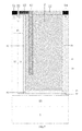
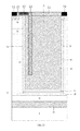
- FIG. 1 is a schematic diagram of a conventional lateral dielectric trench high-voltage device
- FIG. 2 is a schematic diagram of a device structure of the embodiment 1 of the invention, wherein the doping-overlapping structure is located on the left side of the dielectric trench region
- FIG. 3 is a schematic diagram of a device structure of the embodiment 2 of the invention, wherein the doping-overlapping structure is located on the right side of the dielectric trench region;
- FIG. 4 is a schematic diagram of a device structure of the embodiment 3 of the invention, wherein the doping-overlapping structure is located blow the dielectric trench region;
- FIG. 5 is a schematic diagram of a device structure of the embodiment 4 of the invention, wherein the doping-overlapping structures are located on the right side and left side of the dielectric trench region;
- FIG. 6 is a schematic diagram of a device structure of the embodiment 5 of the invention, wherein the doping-overlapping structures are located on the right side of, on the left side of, and below the dielectric trench region;
- FIG. 7 is a schematic diagram of a device structure of the embodiment 6 of the invention, wherein an epitaxial layer is located between the P-type substrate and the conductive path;
- FIG. 8 is a schematic diagram of a device structure with a shallow trench gate in the embodiment 7 of the invention.
- FIG. 9 is a schematic diagram of a device structure with a trench gate in the embodiment 8 of the invention.
- FIG. 10 is a schematic diagram of a device structure of the embodiment 9 of the invention, wherein a trench gate is located in the dielectric trench region;
- FIG. 11 is a schematic diagram of a LIGBT device of the embodiment 10 of the invention.
- FIG. 12 is a schematic diagram of a SOI device without epitaxial layer of the embodiment 11 of the invention.
- FIG. 13 is a schematic diagram of a SOI device with an epitaxial layer of the embodiment 12 of the invention.
- FIG. 14 is a schematic diagram of a device of the embodiment 13 of the invention, wherein the dielectric trench region is composed of two dielectric media having different dielectric constants;
- FIG. 15 is a schematic diagram of a device of the embodiment 14 of the invention, wherein the dielectric trench region is composed of three dielectric media having different dielectric constants;
- FIG. 16 is a schematic diagram of a device of the embodiment 15 of the invention, wherein the drain terminal introduces the drain terminal field;
- FIG. 17 is a schematic diagram of a device simulation structure of the embodiment 13 of the invention.
- FIG. 18 is the on state current distribution diagram of the device simulation of the embodiment 13 of the invention:
- FIG. 19 is the on state linear region current diagram of the device simulation of the embodiment 13 of the invention.
- FIG. 20 is the off state BV diagram of the device simulation of the embodiment 13 of the invention.
- 1 is the P-type substrate
- 2 is the dielectric trench region
- 21 is the gate oxide layer
- 22 is the dielectric layer
- 23 is the SOI oxygen layer
- 31 is the first N-type heavy doping region
- 32 is the first N-type doping pillar
- 33 is the second N-type doping pillar
- 34 is the third N-type doping pillar
- 35 is the second N-type heavy doping region
- 36 is the fourth N-type doping pillar
- 37 is the fifth N-type doping pillar.
- 38 is the sixth N-type doping pillar
- 39 is the seventh N-type doping pillar
- 41 is the P-type heavy doping region
- 42 is P-well region
- 43 is the first P-type doping pillar
- 44 is the second P-type doping pillar
- 45 is the third P-type doping pillar
- 46 is the epitaxial layer
- 47 is the collector terminal P-type heavy doping region
- 51 is the source contacting terminal
- 52 is the polysilicon gate
- 53 is the body field plate
- 54 is the drain contacting terminal
- 55 is the low-K dielectric trench
- 56 is the dielectric trench
- 57 is the second dielectric trench
- 58 is the electrode field plate.
- the dielectric trench region By adding the dielectric trench region into the drift region, the dielectric trench region is subjected to lateral pressure while reducing device size, and thus the specific On-Resistance R ON,sp of the device is also reduced.
- the heavy doping N-type doping pillars are introduced into the drift region, providing low resistance conductive pathway for the on-state electronic current of the device, and further reducing the specific On-Resistance R ON,sp of the device.
- the body field plate 53 is introduced into the dielectric trench region for the auxiliary depletion of the heavy doping N-type doping pillars to improve the breakdown Voltage BV of the device.
- the heavy doping P-type doping pillars are also introduced into the drift region, so that while the N-type doping pillars are depleted when the state is off, an additional electric field is formed to improve the breakdown Voltage BV of the device.
- FIG. 18 is an on state current distribution diagram of the trench type lateral high-voltage device of the invention. As the diagram shows, when the device is in on state, the current is distributed in two low resistance conductive pathways provided by the N-type heavy doping pillars, so that the current capacity is enhanced when the surface area is unchanged, i.e., the specific On-Resistance R ON,sp of the device is reduced when the surface area is unchanged.
- FIG. 19 is the current diagram of the on state linear region of the structural device of the invention. By MEDICI device simulation, a sample structure of the present invention has a 27% reduction in its linear resistance compared with the traditional structure.
- FIG. 20 is the off state BV diagram of the structure device simulation of the invention. As to an exemplary structure of the present invention, the breakdown Voltage BV has an increase of about 140V compared with the traditional structure. The invention can greatly reduce the specific On-Resistance R ON,sp while obtaining a high breakdown Voltage BV.
- a lateral high-voltage device comprising: a dielectric trench region 2 , a doping-overlapping structure with different doping types in an alternating mode is provided on the left side of the dielectric trench region 2 .
- the doping-overlapping structure includes the first N-type doping pillar 32 , the first P-type doping pillar 43 and a fifth N-type doping pillar 37 , and there is a fourth N-type doping pillar 36 between the doping-overlapping structure and the P-well region 42 .
- the upper surface of the dielectric trench region 2 is a dielectric layer 22 , and a body field plate 53 extends from the surface of the device to the interior of the dielectric trench region 2 .
- the body field plate 53 is adjacently connected to a polysilicon gate 52 , the gate oxide layer 21 is located below the polysilicon gate 52 .
- a source contacting terminal 51 and the polysilicon gate 52 are isolated through the dielectric layer 22 .
- the body field plate 53 and a drain contacting terminal 54 are isolated through the dielectric layer 22 .
- a second N-type heavy doping region 35 is below the drain contacting terminal 54 .
- An adjacent P-type heavy doping region 41 and a first n-type heavy doping region 31 are below the source contacting terminal 51 .
- the P-type heavy doping region 41 and the first N-type heavy doping region 31 are positioned in the P well region 42 and at the top of the P well region 42 .
- the gate oxide layer 21 is positioned above the P-well region 42 .
- a conductive pathway consisting of a first N-type doping pillar 32 , a second N-type doping pillar 33 and a third N-type doping pillar 34 are respectively provided on two sides of and below the dielectric trench region 2 .
- a first P-type doping pillar 43 and a second P-type doping pillar 44 are respectively provided on two sides of the conductive pathway.
- a P-type substrate 1 is below the conductive pathway.
- a pair of adjacent N-type doping pillar and P-type doping pillar constitutes one group.
- the doping-overlapping structure includes a plurality of groups with N-type doping pillars and P-type doping pillars in an alternating mode, wherein the number of groups are more than 2.
- the N-type doping pillars can have different widths as the P-type doping pillars.
- the embodiment 2 and embodiment 1 are essentially the same, except that: the doping-overlapping structure is on the right side of the dielectric trench region 2 .
- the doping-overlapping structure sequentially includes the second N-type doping pillar 33 , the second P-type doping pillar 44 and the seventh N-Type doping pillar 39 .
- the upper surfaces of N-type doping pillar 33 , P-type doping pillar 44 and N-type doping pillar 39 contact with the second N-type heavy doping region 35 .
- the embodiment 3 and embodiment 1 are essentially the same, except that: the doping-overlapping structure is below the dielectric trench region 2 .
- the doping-overlapping structure sequentially includes the third N-type doping pillar 34 , the third P-type doping pillar 45 and the sixth N-type doping pillar 38 .
- the embodiment 4 and embodiment 1 are essentially the same, except that: the doping-overlapping structures are on the right side and left side of the dielectric trench region 2 .
- the doping-overlapping structure on the right side of the dielectric trench region 2 sequentially includes the second N-type doping pillar 33 , the second P-type doping pillar 44 and the seventh N-Type doping pillar 39 .
- the upper surfaces of N-type doping pillar 33 , P-type doping pillar 44 and N-type doping pillar 39 contact with the second N-type heavy doping region 35 .
- the doping-overlapping structure on the left side of the dielectric trench region 2 sequentially includes the first N-type doping pillar 32 , the first P-type doping pillar 43 and the fifth N-type doping pillar 37 , and there is a fourth N-type doping pillar 36 between the doping-overlapping structure and the P-well region 42 .
- the embodiment 5 and embodiment 1 are essentially the same, except that: the doping-overlapping structures are on the right side of, on the left side of and below the dielectric trench region 2 .
- the doping-overlapping structure below the dielectric trench region 2 sequentially includes the third N-type doping pillar 34 , the third P-type doping pillar 45 and the sixth N-type doping pillar 38 .
- the doping-overlapping structure on the right side of the dielectric trench region 2 sequentially includes the second N-type doping pillar 33 , the second P-type doping pillar 44 and the seventh N-Type doping pillar 39 , and the upper surfaces of the N-type doping pillar 33 , P-type doping pillar 44 and N-type doping pillar 39 contact with the second N-type heavy doping region 35 .
- the doping-overlapping structure on the left side of the dielectric trench region 2 sequentially includes the first N-type doping pillar 32 , the first P-type doping pillar 43 and the fifth N-type doping pillar 37 , and there is a fourth N-type doping pillar 36 between the doping-overlapping structure and the P-well region 42 .
- the embodiment 6 and embodiment 5 are essentially the same (there are doping-overlapping structures on the right side of, on the left side of and below the dielectric trench region 2 ), except that: there is an epitaxial layer 46 between the P-type substrate 1 and the conductive pathway.
- the embodiment 7 and embodiment 5 are essentially the same (there are doping-overlapping structures on the right side of, on the left side of and below the dielectric trench region 2 ), except that: the polysilicon gate 52 and the gate oxide layer 21 constitute a trench gate, and the source contacting terminal 51 and the body field plate 53 are adjacent.
- the embodiment 8 and embodiment 7 are essentially the same, except that: the trench gate consisting of the polysilicon gate 52 and the gate oxide layer 21 extends to the interior of the P-type substrate 1 , and the source contacting terminal 51 and the body field plate 53 are adjacent.
- the embodiment 9 and embodiment 7 are essentially the same, except that: the trench gate consisting of the polysilicon gate 52 and the gate oxide layer 21 is arranged inside the dielectric trench region 2 .
- the embodiment 10 and embodiment 5 are essentially the same, except that: the second N-type heavy doping region 35 is replaced by the collector P-type heavy doping region 47 , so the device is changed from a LDMOS device to a LIGBT device.
- the embodiment 11 and embodiment 5 are essentially the same, except that: the device is a SOI device.
- the SOI buried oxygen layer 23 is below the doping-overlapping structure, which is below the dielectric trench region 2 .
- the substrate 1 is N-type silicon or P-type silicon for SOI devices.
- the embodiment 12 and embodiment 11 are essentially the same, except that: the device is a SOI device.
- the epitaxial layer 46 is below the doping-overlapping structure, which is below the dielectric trench region 2 .
- the epitaxial layer 46 is arranged between the SOI buried oxygen layer 23 and the conductive pathway.
- the embodiment 13 and embodiment 5 are essentially the same (there are doping-overlapping structures on the right side of, on the left side of and below the dielectric trench region 2 ), except that: the dielectric trench region 2 comprises a low-K dielectric trench 55 in the upper portion and the dielectric trench 56 in the lower portion.
- the low-k dielectric refers to the dielectric having a dielectric constant lower than the that of SiO 2 .
- the embodiment 14 and embodiment 13 are essentially the same (there are doping-overlapping structures on the right side of, on the left side of and below the dielectric trench region 2 ), except that: the dielectric trench region 2 is divided into a plurality of dielectric regions with different dielectric constants, and the dielectric constant in each dielectric area is raised in turn from top to bottom. This will introduce a plurality of electric field peaks, further enhancing the breakdown voltage BV of the device.
- Dielectric trench 57 is below the dielectric trench 55 , and the dielectric constant of the dielectric trench 57 is higher than that of the low-K dielectric trench 55 .
- the dielectric constant of the dielectric trench 56 is higher than that of the second dielectric trench 57 .
- a new electric field peak is introduced due to the intersection of dielectric media having different dielectric constants, greatly improving the breakdown voltage BV of the device.
- the embodiment 15 and embodiment 13 are essentially the same, except that: the left side of drain contacting terminal 54 contacts with the electrode field plate 58 , and the electrode field plate 58 extends from the surface of the device to the interior of the dielectric trench region.
Abstract
Description
Claims (12)
Applications Claiming Priority (4)
| Application Number | Priority Date | Filing Date | Title |
|---|---|---|---|
| CN201710495848 | 2017-06-26 | ||
| CN201710496712.0A CN107275388B (en) | 2017-06-26 | 2017-06-26 | Transverse high-voltage device |
| CN201710496712 | 2017-06-26 | ||
| CN201710495848.XA CN107195683A (en) | 2017-06-26 | 2017-06-26 | A kind of lateral high-voltage device |
Publications (1)
| Publication Number | Publication Date |
|---|---|
| US10068965B1 true US10068965B1 (en) | 2018-09-04 |
Family
ID=63295394
Family Applications (1)
| Application Number | Title | Priority Date | Filing Date |
|---|---|---|---|
| US15/718,001 Expired - Fee Related US10068965B1 (en) | 2017-06-26 | 2017-09-28 | Lateral high-voltage device |
Country Status (1)
| Country | Link |
|---|---|
| US (1) | US10068965B1 (en) |
Cited By (6)
| Publication number | Priority date | Publication date | Assignee | Title |
|---|---|---|---|---|
| CN110504321A (en) * | 2019-08-27 | 2019-11-26 | 杭州电子科技大学温州研究院有限公司 | Silicon ldmos transistor on a kind of insulating layer with PN column |
| US20200020573A1 (en) * | 2018-07-11 | 2020-01-16 | Vanguard International Semiconductor Corporation | Semiconductor substrate structure and semiconductor device and methods for forming the same |
| CN112885889A (en) * | 2021-01-14 | 2021-06-01 | 电子科技大学 | Transverse pressure-resistant area containing combined medium deep groove |
| CN113206145A (en) * | 2021-04-22 | 2021-08-03 | 电子科技大学 | Power semiconductor device with improved hot carrier injection |
| CN113517354A (en) * | 2021-04-29 | 2021-10-19 | 电子科技大学 | High-voltage JFET device |
| CN114899103A (en) * | 2022-07-13 | 2022-08-12 | 北京芯可鉴科技有限公司 | Silicon carbide LDMOSFET device manufacturing method and silicon carbide LDMOSFET device |
Citations (7)
| Publication number | Priority date | Publication date | Assignee | Title |
|---|---|---|---|---|
| US20060038224A1 (en) * | 2004-08-18 | 2006-02-23 | Shibib Muhammed A | Metal-oxide-semiconductor device having an enhanced shielding structure |
| US20070102773A1 (en) * | 2005-11-09 | 2007-05-10 | Kabushiki Kaisha Toshiba | Semiconductor device and method of manufacturing same |
| US20080135930A1 (en) * | 2006-11-14 | 2008-06-12 | Kabushiki Kaisha Toshiba | Power semiconductor device |
| US20090032865A1 (en) * | 2007-07-18 | 2009-02-05 | Infineon Technologies Austria Ag | Semiconductor component and method for producing it |
| US20130334601A1 (en) * | 2011-09-21 | 2013-12-19 | Globalfoundries Singapore Pte. Ltd. | High voltage trench transistor |
| US20170148871A1 (en) * | 2014-05-30 | 2017-05-25 | Texas Instruments Incorporated | Mosfet having dual-gate cells with an integrated channel diode |
| US20170263727A1 (en) * | 2011-09-23 | 2017-09-14 | Alpha And Omega Semiconductor Incorporated | Lateral pnp bipolar transistor with narrow trench emitter |
-
2017
- 2017-09-28 US US15/718,001 patent/US10068965B1/en not_active Expired - Fee Related
Patent Citations (8)
| Publication number | Priority date | Publication date | Assignee | Title |
|---|---|---|---|---|
| US20060038224A1 (en) * | 2004-08-18 | 2006-02-23 | Shibib Muhammed A | Metal-oxide-semiconductor device having an enhanced shielding structure |
| US20070102773A1 (en) * | 2005-11-09 | 2007-05-10 | Kabushiki Kaisha Toshiba | Semiconductor device and method of manufacturing same |
| US20080135930A1 (en) * | 2006-11-14 | 2008-06-12 | Kabushiki Kaisha Toshiba | Power semiconductor device |
| US20090032865A1 (en) * | 2007-07-18 | 2009-02-05 | Infineon Technologies Austria Ag | Semiconductor component and method for producing it |
| US20130334601A1 (en) * | 2011-09-21 | 2013-12-19 | Globalfoundries Singapore Pte. Ltd. | High voltage trench transistor |
| US20150236085A1 (en) * | 2011-09-21 | 2015-08-20 | Globalfoundries Singapore Pte. Ltd. | High voltage trench transistor |
| US20170263727A1 (en) * | 2011-09-23 | 2017-09-14 | Alpha And Omega Semiconductor Incorporated | Lateral pnp bipolar transistor with narrow trench emitter |
| US20170148871A1 (en) * | 2014-05-30 | 2017-05-25 | Texas Instruments Incorporated | Mosfet having dual-gate cells with an integrated channel diode |
Cited By (12)
| Publication number | Priority date | Publication date | Assignee | Title |
|---|---|---|---|---|
| US20200020573A1 (en) * | 2018-07-11 | 2020-01-16 | Vanguard International Semiconductor Corporation | Semiconductor substrate structure and semiconductor device and methods for forming the same |
| US10658228B2 (en) * | 2018-07-11 | 2020-05-19 | Vanguard International Semiconductor Corporation | Semiconductor substrate structure and semiconductor device and methods for forming the same |
| CN110504321A (en) * | 2019-08-27 | 2019-11-26 | 杭州电子科技大学温州研究院有限公司 | Silicon ldmos transistor on a kind of insulating layer with PN column |
| CN110504321B (en) * | 2019-08-27 | 2022-03-01 | 杭州电子科技大学温州研究院有限公司 | Silicon-on-insulator LDMOS transistor with PN column |
| CN112885889A (en) * | 2021-01-14 | 2021-06-01 | 电子科技大学 | Transverse pressure-resistant area containing combined medium deep groove |
| CN112885889B (en) * | 2021-01-14 | 2022-06-03 | 电子科技大学 | Transverse pressure-resistant area containing combined medium deep groove |
| CN113206145A (en) * | 2021-04-22 | 2021-08-03 | 电子科技大学 | Power semiconductor device with improved hot carrier injection |
| CN113206145B (en) * | 2021-04-22 | 2022-08-05 | 电子科技大学 | Power semiconductor device with improved hot carrier injection |
| CN113517354A (en) * | 2021-04-29 | 2021-10-19 | 电子科技大学 | High-voltage JFET device |
| CN113517354B (en) * | 2021-04-29 | 2023-04-28 | 电子科技大学 | High-voltage JFET device |
| CN114899103A (en) * | 2022-07-13 | 2022-08-12 | 北京芯可鉴科技有限公司 | Silicon carbide LDMOSFET device manufacturing method and silicon carbide LDMOSFET device |
| CN114899103B (en) * | 2022-07-13 | 2022-09-13 | 北京芯可鉴科技有限公司 | Silicon carbide LDMOSFET device manufacturing method and silicon carbide LDMOSFET device |
Similar Documents
| Publication | Publication Date | Title |
|---|---|---|
| US10068965B1 (en) | Lateral high-voltage device | |
| US7535057B2 (en) | DMOS transistor with a poly-filled deep trench for improved performance | |
| US8716794B2 (en) | SOI lateral MOSFET devices | |
| US20210074853A1 (en) | Semiconductor Device and Manufacturing Method | |
| US6833585B2 (en) | High voltage lateral DMOS transistor having low on-resistance and high breakdown voltage | |
| US6825536B2 (en) | Lateral power MOSFET for high switching speeds | |
| US9362351B2 (en) | Field effect transistor, termination structure and associated method for manufacturing | |
| US9496382B2 (en) | Field effect transistor, termination structure and associated method for manufacturing | |
| US20130161740A1 (en) | Lateral High-Voltage Transistor with Buried Resurf Layer and Associated Method for Manufacturing the Same | |
| KR20130085751A (en) | Lateral dmos transistor and method of fabricating the same | |
| US8482066B2 (en) | Semiconductor device | |
| CN107275388B (en) | Transverse high-voltage device | |
| CN104752512A (en) | Transverse high-voltage device with multi-electrode structure | |
| CN101593773B (en) | Trench-type power mos transistor and integrated circuit utilizing the same | |
| TWI447912B (en) | Semiconductor device and manufacturing method for the same | |
| KR20120108899A (en) | Semiconductor apparatus | |
| TW201810691A (en) | Diode, junction field effect transistor, and semiconductor device | |
| US20140124858A1 (en) | Semiconductor device and fabricating method thereof | |
| TWI473267B (en) | Mosfet device | |
| CN112909082B (en) | High-voltage low-resistance power LDMOS | |
| CN107146814B (en) | High voltage semiconductor device and method for manufacturing the same | |
| US11316021B2 (en) | High density power device with selectively shielded recessed field plate | |
| CN109616522B (en) | Transverse high-voltage device | |
| CN112186028A (en) | Shielding grid MOSFET device integrated with NPN punch-through triode | |
| TWI641131B (en) | Lateral double-diffused metal oxide semiconductor device |
Legal Events
| Date | Code | Title | Description |
|---|---|---|---|
| FEPP | Fee payment procedure |
Free format text: ENTITY STATUS SET TO UNDISCOUNTED (ORIGINAL EVENT CODE: BIG.); ENTITY STATUS OF PATENT OWNER: SMALL ENTITY |
|
| FEPP | Fee payment procedure |
Free format text: ENTITY STATUS SET TO SMALL (ORIGINAL EVENT CODE: SMAL); ENTITY STATUS OF PATENT OWNER: SMALL ENTITY |
|
| STCF | Information on status: patent grant |
Free format text: PATENTED CASE |
|
| FEPP | Fee payment procedure |
Free format text: MAINTENANCE FEE REMINDER MAILED (ORIGINAL EVENT CODE: REM.); ENTITY STATUS OF PATENT OWNER: SMALL ENTITY |
|
| LAPS | Lapse for failure to pay maintenance fees |
Free format text: PATENT EXPIRED FOR FAILURE TO PAY MAINTENANCE FEES (ORIGINAL EVENT CODE: EXP.); ENTITY STATUS OF PATENT OWNER: SMALL ENTITY |
|
| STCH | Information on status: patent discontinuation |
Free format text: PATENT EXPIRED DUE TO NONPAYMENT OF MAINTENANCE FEES UNDER 37 CFR 1.362 |
|
| FP | Lapsed due to failure to pay maintenance fee |
Effective date: 20220904 |