JP6842485B2 - LED module - Google Patents
LED module Download PDFInfo
- Publication number
- JP6842485B2 JP6842485B2 JP2019038818A JP2019038818A JP6842485B2 JP 6842485 B2 JP6842485 B2 JP 6842485B2 JP 2019038818 A JP2019038818 A JP 2019038818A JP 2019038818 A JP2019038818 A JP 2019038818A JP 6842485 B2 JP6842485 B2 JP 6842485B2
- Authority
- JP
- Japan
- Prior art keywords
- pad
- main surface
- led chip
- circular
- electrode
- Prior art date
- Legal status (The legal status is an assumption and is not a legal conclusion. Google has not performed a legal analysis and makes no representation as to the accuracy of the status listed.)
- Active
Links
- 239000000758 substrate Substances 0.000 claims description 104
- 230000000149 penetrating effect Effects 0.000 claims description 5
- 239000010410 layer Substances 0.000 description 54
- 229920005989 resin Polymers 0.000 description 35
- 239000011347 resin Substances 0.000 description 35
- 239000012790 adhesive layer Substances 0.000 description 18
- 229910000679 solder Inorganic materials 0.000 description 15
- 238000000034 method Methods 0.000 description 10
- 238000004519 manufacturing process Methods 0.000 description 9
- 238000000926 separation method Methods 0.000 description 9
- 238000007789 sealing Methods 0.000 description 8
- 239000000853 adhesive Substances 0.000 description 7
- 230000001070 adhesive effect Effects 0.000 description 7
- 239000007788 liquid Substances 0.000 description 6
- 239000004065 semiconductor Substances 0.000 description 6
- 239000000463 material Substances 0.000 description 5
- 239000003822 epoxy resin Substances 0.000 description 4
- 239000010931 gold Substances 0.000 description 4
- 239000013067 intermediate product Substances 0.000 description 4
- 229920000647 polyepoxide Polymers 0.000 description 4
- PXHVJJICTQNCMI-UHFFFAOYSA-N Nickel Chemical compound [Ni] PXHVJJICTQNCMI-UHFFFAOYSA-N 0.000 description 3
- 230000005540 biological transmission Effects 0.000 description 3
- 239000010949 copper Substances 0.000 description 3
- PCHJSUWPFVWCPO-UHFFFAOYSA-N gold Chemical compound [Au] PCHJSUWPFVWCPO-UHFFFAOYSA-N 0.000 description 3
- 229910052737 gold Inorganic materials 0.000 description 3
- 238000007747 plating Methods 0.000 description 3
- RYGMFSIKBFXOCR-UHFFFAOYSA-N Copper Chemical compound [Cu] RYGMFSIKBFXOCR-UHFFFAOYSA-N 0.000 description 2
- 229920000106 Liquid crystal polymer Polymers 0.000 description 2
- 239000004977 Liquid-crystal polymers (LCPs) Substances 0.000 description 2
- 239000004954 Polyphthalamide Substances 0.000 description 2
- BQCADISMDOOEFD-UHFFFAOYSA-N Silver Chemical compound [Ag] BQCADISMDOOEFD-UHFFFAOYSA-N 0.000 description 2
- 230000001154 acute effect Effects 0.000 description 2
- 238000004891 communication Methods 0.000 description 2
- 229910052802 copper Inorganic materials 0.000 description 2
- 230000000694 effects Effects 0.000 description 2
- 239000011521 glass Substances 0.000 description 2
- 239000011810 insulating material Substances 0.000 description 2
- 238000009413 insulation Methods 0.000 description 2
- 229920006375 polyphtalamide Polymers 0.000 description 2
- 229910052709 silver Inorganic materials 0.000 description 2
- 239000004332 silver Substances 0.000 description 2
- NIXOWILDQLNWCW-UHFFFAOYSA-N acrylic acid group Chemical group C(C=C)(=O)O NIXOWILDQLNWCW-UHFFFAOYSA-N 0.000 description 1
- 238000005452 bending Methods 0.000 description 1
- 238000007796 conventional method Methods 0.000 description 1
- 230000012447 hatching Effects 0.000 description 1
- 238000009434 installation Methods 0.000 description 1
- 229910052759 nickel Inorganic materials 0.000 description 1
- 230000035515 penetration Effects 0.000 description 1
- 230000000717 retained effect Effects 0.000 description 1
- 229920002050 silicone resin Polymers 0.000 description 1
Images


Description
本発明は、LEDモジュールに関する。 The present invention relates to an LED module.
図32は、従来のLEDモジュールの一例を示している(たとえば、特許文献1参照)。同図に示されたLEDモジュール900は、長矩形状の基板910に3つのLEDチップ931,932,933が搭載された構造とされている。基板910には、複数の電極921,922,922,924が形成されている。電極921,922,923には、LEDチップ921,922,923がそれぞれダイボンディングされている。電極924は、いわゆるコモン電極であり、LEDチップ931,932,933のそれぞれに対してワイヤを介して導通している。3つのLEDチップ931,932,933は、ケース950によって囲われている。ケース950は、略枠状の不透光樹脂製であり、その内側空間に透光樹脂(図示略)が充填されている。LEDモジュール900は、基板910の長手方向に延びる図中下方の面を実装面として実装基板などに実装される、いわゆるサイドビュータイプのLEDモジュールとして構成されている。LEDチップ931,932,933は、それぞれ赤色光、緑色光、青色光を出射するものである。これらのLEDチップ931,932,933からの光を混色させることにより、LEDモジュール900は、白色光を出射することが指向されている。
FIG. 32 shows an example of a conventional LED module (see, for example, Patent Document 1). The
しかしながら、LEDモジュール900に対する小型化の要請は年々強くなっている。たとえば、LEDモジュール900が実装される実装基板からの突出高さを抑制しようとすると、基板910を更に狭幅化する必要がある。これに伴い、LEDチップ931,932,933を搭載するためのスペースが狭くなる。LEDチップ931,932,933を搭載するためのスペースとしては、LEDチップ931,932,933自体の設置スペースの他に、これらに接続されたワイヤ、およびコモン電極924のうちこれらのワイヤが接続された部分を配置するためのスペースが必要である。また、基板910において電極922,923が占める割合は決して小さくない。このため、基板910を狭幅化することは容易ではなかった。
However, the demand for miniaturization of the
また、上記のサイドビュータイプのLEDモジュールの他に、トップビュータイプのLEDモジュールも知られている。トップビュータイプも小型化を求められている。トップビュータイプのLEDモジュールに関しては、たとえば、特許文献1に開示されている。
In addition to the side-view type LED module described above, a top-view type LED module is also known. The top view type is also required to be miniaturized. A top view type LED module is disclosed in, for example,
本発明は、上記した事情のもとで考え出されたものであって、小型化を図ることのできるLEDモジュールを提供することをその主たる課題とする。 The present invention has been conceived under the above circumstances, and its main object is to provide an LED module capable of miniaturization.
本発明の第1の側面によると、互いに反対側を向く主面および裏面を有する基板と、上記主面に形成された主面電極と、上記主面電極につながり且つ上記基板を貫通する複数の貫通電極と、上記主面電極に第1方向に沿って配列された複数のLEDチップと、上記主面に配置され且つ上記主面電極を囲むケースと、を備え、上記複数のLEDチップのうちの3つは、赤色光、緑色光、および青色光をそれぞれ発する、LEDモジュールが提供される。 According to the first aspect of the present invention, a substrate having a main surface and a back surface facing opposite sides, a main surface electrode formed on the main surface, and a plurality of substrates connected to the main surface electrode and penetrating the substrate. Among the plurality of LED chips, the penetrating electrode, a plurality of LED chips arranged on the main surface electrode along the first direction, and a case arranged on the main surface and surrounding the main surface electrode are provided. Three of these are provided with LED modules that emit red light, green light, and blue light, respectively.
好ましくは、上記主面電極は、上記主面と上記ケースとの間に介在している部位を有する。 Preferably, the main surface electrode has a portion interposed between the main surface and the case.
好ましくは、上記複数のLEDチップのいずれか一つと上記主面電極とに各々がボンディングされた複数のワイヤを更に備える。 Preferably, a plurality of wires each bonded to any one of the plurality of LED chips and the main surface electrode are further provided.
好ましくは、上記裏面に形成され且つ上記複数の貫通電極の各々につながる裏面電極と、上記裏面に形成された絶縁膜と、を更に備える。 Preferably, a back surface electrode formed on the back surface and connected to each of the plurality of through electrodes, and an insulating film formed on the back surface are further provided.
好ましくは、上記ワイヤの端部は、上記基板の厚さ方向視において、上記裏面電極もしくは上記絶縁膜に重なる。 Preferably, the end of the wire overlaps the back electrode or the insulating film in the thickness direction of the substrate.
好ましくは、上記絶縁膜は、全体にわたって、上記基板の厚さ方向視において、上記裏面のうち上記裏面電極が形成された領域以外の領域に形成されている。 Preferably, the insulating film is formed in a region of the back surface other than the region where the back surface electrode is formed in the thickness direction of the substrate as a whole.
好ましくは、上記裏面電極は、互いに離間している複数の実装パッド部を含み、上記絶縁膜は、長手状に延びる第1帯状絶縁部を含み、上記第1帯状絶縁部は、上記複数の実装パッド部のいずれか2つに挟まれた位置に配置されている。 Preferably, the back surface electrode includes a plurality of mounting pad portions separated from each other, the insulating film includes a first strip-shaped insulating portion extending in a longitudinal shape, and the first strip-shaped insulating portion includes the plurality of mounting portions. It is arranged at a position sandwiched between any two of the pad portions.
好ましくは、上記裏面は、上記絶縁膜から露出する露出部を有し、上記露出部は、上記第1帯状絶縁部が延びる方向における上記裏面のうちの端に位置し、上記第1帯状絶縁部は、上記基板の厚さ方向視において上記露出部に連続している。 Preferably, the back surface has an exposed portion exposed from the insulating film, and the exposed portion is located at an end of the back surface in the direction in which the first band-shaped insulating portion extends, and the first band-shaped insulating portion is located. Is continuous with the exposed portion in the thickness direction of the substrate.
好ましくは、上記絶縁膜は、上記第1帯状絶縁部が延びる方向とは交差する方向に、長手状に延びる第2帯状絶縁部を含み、上記第2帯状絶縁部は、上記複数の実装パッド部のいずれか2つに挟まれた位置に配置されている。 Preferably, the insulating film includes a second strip-shaped insulating portion extending in a longitudinal direction in a direction intersecting the direction in which the first strip-shaped insulating portion extends, and the second strip-shaped insulating portion includes the plurality of mounting pad portions. It is arranged at a position sandwiched between any two of the above.
好ましくは、上記第2帯状絶縁部は、上記裏面の端縁に至っている。 Preferably, the second strip-shaped insulating portion reaches the edge of the back surface.
好ましくは、上記主面電極は、第1導電部と、上記第1導電部から絶縁された第2導電部と、を含み、上記第1導電部には、上記複数のLEDチップのいずれか一つが配置されている。 Preferably, the main surface electrode includes a first conductive portion and a second conductive portion insulated from the first conductive portion, and the first conductive portion includes any one of the plurality of LED chips. One is arranged.
好ましくは、上記第1導電部は、第1ダイパッドと、上記第1ダイパッドに導通している第1ワイヤボンディングパッドと、を有し、上記第1ダイパッドには、上記複数のLEDチップのいずれか一つが配置され、上記第1ワイヤボンディングパッドには、上記複数のワイヤのいずれか一つがボンディングされ、上記第1ダイパッドは、上記第1ワイヤボンディングパッドに対し隙間を介して離間している。 Preferably, the first conductive portion includes a first die pad and a first wire bonding pad conducting the first die pad, and the first die pad is any one of the plurality of LED chips. One is arranged, any one of the plurality of wires is bonded to the first wire bonding pad, and the first die pad is separated from the first wire bonding pad via a gap.
好ましくは、上記第1ワイヤボンディングパッドは、上記第1ダイパッドに対し、上記第1方向に交差する第2方向に離間している。 Preferably, the first wire bonding pad is separated from the first die pad in a second direction intersecting the first direction.
好ましくは、上記第1ダイパッドは、上記第2導電部と、上記第1ワイヤボンディングパッドと、の間に位置する。 Preferably, the first die pad is located between the second conductive portion and the first wire bonding pad.
好ましくは、上記第1導電部は、上記基板の厚さ方向視において上記複数の貫通電極のいずれか一つに重なる第1円形パッドを有し、上記第1円形パッドは、上記第1ワイヤボンディングパッドに導通している。 Preferably, the first conductive portion has a first circular pad that overlaps with any one of the plurality of through electrodes in the thickness direction of the substrate, and the first circular pad is the first wire bonding. Conducting to the pad.
好ましくは、上記第1円形パッドは、上記ケースと上記基板との間に介在している部位を有する。 Preferably, the first circular pad has a portion interposed between the case and the substrate.
好ましくは、上記第1導電部は、上記第1ダイパッドに導通する帯状部を有する。 Preferably, the first conductive portion has a strip-shaped portion that conducts to the first die pad.
好ましくは、上記第2導電部は、上記複数のワイヤのいずれか一つがボンディングされたワイヤボンディング配線部を有する。 Preferably, the second conductive portion has a wire bonding wiring portion to which any one of the plurality of wires is bonded.
好ましくは、上記第2導電部には、上記複数のワイヤのいずれか一つがボンディングされている。 Preferably, any one of the plurality of wires is bonded to the second conductive portion.
好ましくは、上記第2導電部は、上記基板の厚さ方向視において上記複数の貫通電極のいずれか一つに重なる第2円形配線部を有し、上記第2円形配線部は、上記ワイヤボンディング配線部に導通している。 Preferably, the second conductive portion has a second circular wiring portion that overlaps with any one of the plurality of through electrodes in the thickness direction of the substrate, and the second circular wiring portion is wire bonding. It is conducting to the wiring part.
好ましくは、上記第2円形配線部は、上記ワイヤボンディング配線部につながっている。 Preferably, the second circular wiring portion is connected to the wire bonding wiring portion.
好ましくは、上記第2円形配線部は、上記ケースと上記基板との間に介在している部位を有する。 Preferably, the second circular wiring portion has a portion interposed between the case and the substrate.
好ましくは、上記複数のLEDチップのいずれか一つと上記主面電極との間に各々が介在している複数の接合層を更に備える。 Preferably, a plurality of bonding layers are further provided, each of which is interposed between any one of the plurality of LED chips and the main surface electrode.
好ましくは、上記複数の接合層のいずれか一つは、導電性を有する。 Preferably, any one of the plurality of bonding layers has conductivity.
好ましくは、上記複数の接合層のいずれか一つは、絶縁性を有する。 Preferably, any one of the plurality of bonding layers has an insulating property.
好ましくは、上記ケースと上記基板との間に介在している接着層を更に備える。 Preferably, an adhesive layer interposed between the case and the substrate is further provided.
好ましくは、上記複数の貫通電極のいずれか一つは、上記基板の厚さ方向視において、上記ケースに重なる。 Preferably, any one of the plurality of through electrodes overlaps the case in the thickness direction of the substrate.
好ましくは、上記ケースは、上記複数のLEDチップを囲む包囲面を有する。 Preferably, the case has an enclosing surface that surrounds the plurality of LED chips.
好ましくは、上記ケースは、上記包囲面が包囲する領域とは反対側を向くケース側面を有する。 Preferably, the case has a case side that faces away from the area surrounded by the enclosing surface.
好ましくは、上記基板は、上記ケース側面と面一である基板側面を有する。 Preferably, the substrate has a substrate side surface that is flush with the case side surface.
好ましくは、上記ケースは、上記主面に対向し且つ上記包囲面および上記ケース側面とつながる底面を有する。 Preferably, the case has a bottom surface that faces the main surface and connects to the surrounding surface and the side surface of the case.
好ましくは、上記底面は、枠状を呈し、且つ、上記包囲面から上記ケース側面にわたって平坦である。 Preferably, the bottom surface has a frame shape and is flat from the surrounding surface to the side surface of the case.
好ましくは、上記包囲面は、上記底面と鋭角をなすように上記基板の厚さ方向に対し傾斜している。 Preferably, the surrounding surface is inclined with respect to the thickness direction of the substrate so as to form an acute angle with the bottom surface.
好ましくは、上記複数のLEDチップはいずれも、上記第1ダイパッドに配置されている。 Preferably, all of the plurality of LED chips are arranged on the first die pad.
好ましくは、上記複数のワイヤのいずれか一つは、上記基板の厚さ方向視において、上記第1方向と上記第1方向に直交する方向と、に対し傾斜する方向に延びている。 Preferably, any one of the plurality of wires extends in a direction inclined with respect to the first direction and the direction orthogonal to the first direction in the thickness direction of the substrate.
好ましくは、上記第1導電部は、上記第1ダイパッドから離間している第2ダイパッドと、上記第1ダイパッドおよび上記第2ダイパッドのいずれもから離間している第3ダイパッドと、を有し、上記第1ダイパッドには、上記複数のLEDチップのうちの1つのみが配置され、上記第2ダイパッドには、上記複数のLEDチップのうちの1つのみが配置され、上記第3ダイパッドには、上記複数のLEDチップのうちの1つのみが配置されている。 Preferably, the first conductive portion has a second die pad that is separated from the first die pad, and a third die pad that is separated from both the first die pad and the second die pad. Only one of the plurality of LED chips is arranged on the first die pad, only one of the plurality of LED chips is arranged on the second die pad, and the third die pad is arranged with only one of the plurality of LED chips. , Only one of the plurality of LED chips is arranged.
本発明の第2の側面によると、本発明の第2の側面によって提供されるLEDモジュールと、実装基板と、上記実装基板と上記裏面との間に介在しているハンダ層と、を備える、LEDモジュールの実装構造が提供される。 According to the second aspect of the present invention, the LED module provided by the second aspect of the present invention includes a mounting board and a solder layer interposed between the mounting board and the back surface. An LED module mounting structure is provided.
本発明の第3の側面によると、主面を有する基板と、上記主面に形成された主面電極と、上記主面電極につながり且つ上記基板を貫通する複数の貫通電極と、上記主面電極に一方向に沿って配列された複数のLEDチップと、を備え、上記複数のLEDチップどうしの離間距離は、100〜150μmである、LEDモジュールが提供される。 According to the third aspect of the present invention, a substrate having a main surface, a main surface electrode formed on the main surface, a plurality of through electrodes connected to the main surface electrode and penetrating the substrate, and the main surface. Provided is an LED module comprising a plurality of LED chips arranged along one direction on an electrode, and the distance between the plurality of LED chips is 100 to 150 μm.
本発明の第4の側面によると、互いに反対方向を向き長矩形状である主面および背面、これらの主面および背面の長辺どうしをつなぐ底面、を有する基板と、上記基板の上記主面に支持された1以上のLEDチップと、上記基板上に形成されており、上記LEDチップに導通する配線と、を備えており、上記底面を実装面とする、LEDモジュールであって、上記基板は、上記主面から上記背面に貫通する1以上の貫通孔を有し、上記配線は、上記主面に形成されているとともに上記LEDチップに導通するパッド、上記背面に形成された背面電極、上記パッドおよび上記背面電極を導通させているとともに上記貫通孔内面に形成された貫通電極、を有することを特徴とする、LEDモジュールが提供される。 According to the fourth aspect of the present invention, a substrate having a main surface and a back surface which are long rectangular shapes facing in opposite directions, and a bottom surface connecting the long sides of the main surface and the back surface, and the main surface of the substrate. An LED module comprising one or more supported LED chips, a wiring formed on the substrate and conducting conduction to the LED chip, and having the bottom surface as a mounting surface, wherein the substrate is The pad having one or more through holes penetrating from the main surface to the back surface, and the wiring is formed on the main surface and conducting to the LED chip, the back electrode formed on the back surface, and the above. Provided is an LED module characterized by having a pad and a through electrode formed on the inner surface of the through hole while conducting the back electrode.
好ましくは、上記配線は、上記基板の上記底面のすべてを露出させている。 Preferably, the wiring exposes all of the bottom surfaces of the substrate.
好ましくは、上記主面の長手方向に離間配置された3つの上記LEDチップを備える。 Preferably, the three LED chips are spaced apart from each other in the longitudinal direction of the main surface.
好ましくは、上記基板は、3つの上記貫通孔を有し、上記配線は、3つの上記貫通電極を有する。 Preferably, the substrate has three through holes and the wiring has three through electrodes.
好ましくは、上記配線は、上記パッドとしてのボンディングパッドを有しており、上記3つのLEDチップのうちの1つと上記ボンディングパッドとを接続する第1ワイヤを備えており、上記3つの貫通孔の1つと上記ボンディングパッドとが重なっており、かつ上記3つの貫通電極の1つと上記ボンディングパッドとが導通している。 Preferably, the wiring has a bonding pad as the pad, includes a first wire connecting one of the three LED chips and the bonding pad, and of the three through holes. One and the bonding pad overlap each other, and one of the three through electrodes and the bonding pad are conductive.
好ましくは、上記配線は、上記3つのLEDチップのうちの2つがダイボンディングされた上記パッドとしての2つのダイボンディングパッドを有しており、上記2つのダイボンディングパッドと2つの上記貫通孔とが上記基板の厚さ方向視において重なる。 Preferably, the wiring has two die bonding pads as the pads in which two of the three LED chips are die bonded, and the two die bonding pads and the two through holes are formed. They overlap in the thickness direction of the above substrates.
好ましくは、上記背面電極は、各々が上記2つの貫通電極を介して上記2つのダイボンディングパッドと導通する2つの個別電極を有する。 Preferably, the back electrode has two individual electrodes, each of which conducts with the two die bonding pads via the two through electrodes.
好ましくは、上記基板は、上記長手方向両端において上記主面および上記背面をつなぐ1対の側面を有しており、かつ上記側面および上記底面の間に介在しており、かつ上記基板の厚さ方向において上記主面および上記背面に達する2つのコーナー溝が形成されており、上記配線は、上記2つのコーナー溝の内面に形成された2つのコーナー溝配線を有する。 Preferably, the substrate has a pair of side surfaces connecting the main surface and the back surface at both ends in the longitudinal direction, and is interposed between the side surfaces and the bottom surface, and the thickness of the substrate. Two corner grooves are formed to reach the main surface and the back surface in the direction, and the wiring has two corner groove wirings formed on the inner surfaces of the two corner grooves.
好ましくは、上記背面電極は、上記2つのコーナー溝配線の一方につながっているとともに上記3つのLEDチップと導通する端部共通電極と、上記2つのコーナー溝配線の他方につながっているとともに上記3つのLEDチップのいずれか1つに導通する端部個別電極とを有する。 Preferably, the back electrode is connected to one of the two corner groove wirings and is connected to the other end common electrode that conducts with the three LED chips, and the other of the two corner groove wirings. It has an end individual electrode that conducts to any one of the LED chips.
好ましくは、上記配線は、上記背面に形成されており、かつ上記2つの個別電極と導通していない上記貫通電極と上記端部共通電極とをつなぐ背面連絡配線を有している。 Preferably, the wiring has a back connecting wiring that is formed on the back surface and connects the through electrode and the end common electrode that are not conductive to the two individual electrodes.
好ましくは、上記コーナー溝は、断面四半円形状である。 Preferably, the corner groove has a quadrangular cross section.
好ましくは、上記主面に形成されており、上記3つのLEDチップを囲む反射面を有するリフレクタと、上記反射面に囲まれた領域に充填されており、上記3つのLEDチップを覆う透光樹脂部と、を備える。 Preferably, a reflector formed on the main surface and having a reflecting surface surrounding the three LED chips and a translucent resin filled in a region surrounded by the reflecting surfaces and covering the three LED chips. It has a part and.
好ましくは、上記3つのLEDチップのうちの1つと上記ボンディングパッドとを接続する第2ワイヤを更に備え、上記第2ワイヤは、上記基板の厚さ方向視において、上記3つのLEDチップのうち上記第1ワイヤが接続されたLEDチップと重なる部位を有する。 Preferably, a second wire for connecting one of the three LED chips and the bonding pad is further provided, and the second wire is one of the three LED chips in the thickness direction of the substrate. It has a portion that overlaps with the LED chip to which the first wire is connected.
好ましくは、上記3つのLEDチップのうち上記第1ワイヤが接続されたLEDチップの中心は、上記3つのLEDチップのうち上記第2ワイヤが接続されたLEDチップの中心に対し、上記主面の短手方向において、ずれた位置に位置する。 Preferably, the center of the LED chip to which the first wire of the three LED chips is connected is on the main surface of the center of the LED chip to which the second wire of the three LED chips is connected. It is located at a shifted position in the lateral direction.
好ましくは、上記3つの貫通孔のうちの一つは、上記基板の厚さ方向視において、上記3つのLEDチップのうち上記第2ワイヤが接続されたLEDチップに重なる部位と、当該LEDチップからはみ出た部位と、を有する。 Preferably, one of the three through holes is formed from a portion of the three LED chips that overlaps the LED chip to which the second wire is connected and the LED chip in the thickness direction of the substrate. It has a protruding part.
好ましくは、上記背面電極を覆う絶縁膜を更に備える。 Preferably, an insulating film covering the back electrode is further provided.
好ましくは、上記絶縁膜は、上記背面連絡配線を覆っている。 Preferably, the insulating film covers the back surface connecting wiring.
好ましくは、上記絶縁膜は、上記各個別電極の少なくとも一部分ずつを露出させている。 Preferably, the insulating film exposes at least a part of each of the individual electrodes.
好ましくは、上記絶縁膜は、上記各個別電極のうちの、上記背面連絡配線に近接する部分を覆っている。 Preferably, the insulating film covers the portion of each of the individual electrodes that is close to the back surface connecting wiring.
好ましくは、上記絶縁膜は、上記端部共通電極および上記端部個別電極を露出させている。 Preferably, the insulating film exposes the end common electrode and the end individual electrode.
本発明のその他の特徴および利点は、添付図面を参照して以下に行う詳細な説明によって、より明らかとなろう。 Other features and advantages of the present invention will become more apparent with the detailed description given below with reference to the accompanying drawings.
以下、本発明の実施の形態につき、図面を参照して具体的に説明する。 Hereinafter, embodiments of the present invention will be specifically described with reference to the drawings.
図1〜図14を用いて、本発明の第1実施形態について説明する。 The first embodiment of the present invention will be described with reference to FIGS. 1 to 14.
図1に示すLEDモジュールの実装構造B1は、LEDモジュールA1と、実装基板871と、ハンダ層872と、を備える。
The LED module mounting structure B1 shown in FIG. 1 includes an LED module A1, a mounting
実装基板871は、たとえばプリント配線基板である。実装基板871は、たとえば、絶縁基板と、当該絶縁基板に形成されたパターン電極(図示略)とを含む。LEDモジュールA1は実装基板871に搭載されている。LEDモジュールA1と、実装基板871との間には、ハンダ層872が介在している。ハンダ層872は、LEDモジュールA1と実装基板871とを接合している。
The mounting
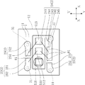
図2は、本実施形態にかかるLEDモジュールの平面図である。図3は、図2から、ケースおよび接着層を省略した平面図である。図4は、本実施形態にかかるLEDモジュールの底面図である。図5は、図2のV−V線に沿う断面図である。図6は、図2のVI−VI線に沿う断面図である。 FIG. 2 is a plan view of the LED module according to the present embodiment. FIG. 3 is a plan view in which the case and the adhesive layer are omitted from FIG. FIG. 4 is a bottom view of the LED module according to the present embodiment. FIG. 5 is a cross-sectional view taken along the line VV of FIG. FIG. 6 is a cross-sectional view taken along the line VI-VI of FIG.
これらの図に示すLEDモジュールA1は、トップビュータイプのものである。すなわち、LEDモジュールA1は実装基板871の厚さ方向に光を放つ。LEDモジュールA1は、基板1と、主面電極2と、複数の貫通電極31と、裏面電極4と、LEDチップ511,512,513と、接合層521,522,523と、封止樹脂部59と、ケース6と、接着層71と、絶縁膜74と、複数のワイヤ81と、を備える。図2においては、理解の便宜上、封止樹脂部59を省略している。また、図5は、図1に示したLEDモジュールA1の拡大図に相当する。図1においては、理解の便宜上、接合層521,522,523および接着層71を省略している。図2、図3では、接合層522,523を省略している。LEDモジュールA1の方向Xおよび方向Yにおける寸法は、たとえば、1.6〜1.8mm程度である。
The LED module A1 shown in these figures is a top view type. That is, the LED module A1 emits light in the thickness direction of the mounting
LEDチップ511,512,513は、LEDモジュールA1の光源である。LEDチップ511,512,513は、p型半導体層とn型半導体層と活性層とが積層された構造である。活性層は、p型半導体層およびn型半導体層に挟まれている。本実施形態においては、LEDチップ511は赤色光を発し、LEDチップ512は緑色光を発し、LEDチップ513は青色光を発する。複数のLEDチップ511,512,513は方向Xに沿って配列されている。LEDチップ511,512,513どうしの離間距離は、100〜150μmであることが好ましい。
The LED chips 511, 512, 513 are light sources of the LED module A1. The LED chips 511, 512, 513 have a structure in which a p-type semiconductor layer, an n-type semiconductor layer, and an active layer are laminated. The active layer is sandwiched between a p-type semiconductor layer and an n-type semiconductor layer. In the present embodiment, the
基板1は、平面視において矩形状を呈する。基板1は、たとえば、ガラスエポキシ樹脂よりなる。基板1は、主面11と、基板側面12と、裏面13と、を有する。主面11および裏面13は互いに反対側を向く。基板側面12は、方向Xのいずれか一方もしくは方向Yのいずれか一方を向く。基板側面12は、主面11および裏面13のいずれともつながっている。主面11、基板側面12、および裏面13はいずれも、平坦である。裏面13と実装基板871との間に、ハンダ層872が介在している。
The
主面電極2は主面11に形成されている。主面電極2は、第1導電部24と、複数の第2導電部25と、を含む。主面電極2は、銅、ニッケル、および金が、互いに積層されている。後述の貫通電極31や裏面電極4も同様である。
The
第1導電部24には、LEDチップ511,512,513のいずれか一つが配置されている。第1導電部24は、ダイパッド241と、ワイヤボンディングパッド242と、円形パッド243と、帯状部244,245と、を有する。
Any one of the LED chips 511, 512, 513 is arranged in the first
ダイパッド241は矩形状を呈する。ダイパッド241には、LEDチップ511,512,513のいずれか一つが配置されている。本実施形態においては、ダイパッド241には、LEDチップ511,512,513のいずれもが配置されている。
The
ワイヤボンディングパッド242は矩形状を呈する。本実施形態においてワイヤボンディングパッド242は、長辺が方向Xに一致する矩形状である。ワイヤボンディングパッド242には、複数のワイヤ81のうちのいずれか1つがボンディングされている。本実施形態においては、ワイヤボンディングパッド242には、複数のワイヤ81のうちの2つがボンディングされている。ワイヤボンディングパッド242に対して隙間を介して、ダイパッド241が離間している。具体的には、ワイヤボンディングパッド242は、ダイパッド241に対し、方向Xに交差する方向Y(本実施形態においては方向Xに直交する)に離間している。ワイヤ81の方向Z視における長さは、たとえば、0.4〜0.6mmである。
The
円形パッド243は方向Z視において円形状を呈する。本実施形態において、円形パッド243は、ダイパッド241に対し、ワイヤボンディングパッド242が位置する側に、配置されている。円形パッド243は、ワイヤボンディングパッド242に対し、方向X側に配置されている。円形パッド243は、ダイパッド241と、ワイヤボンディングパッド242と、に導通している。
The
帯状部244は、方向Yに沿って帯状に延びている。帯状部244は、ダイパッド241に導通している。本実施形態においては、帯状部244は、円形パッド243にも導通している。帯状部244は、ダイパッド241および円形パッド243につながっている。
The band-shaped
帯状部245は、方向Xに沿って帯状に延びている。帯状部245は、ダイパッド241に導通している。本実施形態においては、帯状部245は、円形パッド243にも導通している。帯状部245は、ワイヤボンディングパッド242および円形パッド243につながっている。帯状部245が細ければ細いほど、主面11が露出する面積が大きくなる。帯状部245の反射率よりも主面11の反射率の方が大きい場合、主面11の露出する面積が大きくなることは、LEDモジュールA1の方向Zに向かう光の強度を増大させる点において好ましい。
The band-shaped
以上に述べたように、ダイパッド241と、ワイヤボンディングパッド242と、円形パッド243と、帯状部244,245とは、互いに導通している。
As described above, the
複数(本実施形態においては3つ)の第2導電部25は、それぞれ、第1導電部24から絶縁されている。複数の第2導電部25は、それぞれ、複数のワイヤ81のうちのいずれか1つがボンディングされている。複数の第2導電部25のうちの二つの間に、ダイパッド241が位置している。また、複数の第2導電部25のうちの一つと、ワイヤボンディングパッド242との間には、ダイパッド241が位置している。
A plurality of (three in this embodiment) second
複数の第2導電部25はそれぞれ、ワイヤボンディング配線部251と、円形配線部252と、を有する。
Each of the plurality of second
ワイヤボンディング配線部251は矩形状を呈する。ワイヤボンディング配線部251には、複数のワイヤ81のうちのいずれか1つがボンディングされている。ワイヤボンディング配線部251に対して隙間を介して、ダイパッド241が離間している。具体的には、ワイヤボンディング配線部251は、ダイパッド241に対し、方向Xに交差する方向Y(本実施形態においては方向Xに直交する)に離間している。
The wire
円形配線部252は方向Z視において円形状を呈する。円形配線部252は、ワイヤボンディング配線部251に対し、方向X側に配置されている。円形配線部252は、ワイヤボンディング配線部251に導通している。
The
複数の(本実施形態では5つの)ワイヤ81はそれぞれ、複数のLEDチップ511,512,513のいずれか一つと、主面電極2とにボンディングされている。各ワイヤ81は、金、銀、もしくは銅よりなる。本実施形態では、各ワイヤ81は金よりなる。各ワイヤ81は、基板1の厚さ方向Z視において、方向Xと方向Xに直交する方向Yと、に対し傾斜する方向に延びている。各ワイヤ81の、LEDチップ511,512,513からの高さは、たとえば、110〜130μmである。
Each of the plurality of wires 81 (five in this embodiment) is bonded to any one of the plurality of
接合層521は、LEDチップ511と主面電極2との間に介在している。本実施形態においては、接合層521は、LEDチップ511とダイパッド241(第1導電部24)との間に介在している。接合層521はLEDチップ511を主面電極2(本実施形態においては、ダイパッド241もしくは第1導電部24)に接合するための機能を担う。接合層521は導電性を有する。導電性を有する接合層521を形成するには、たとえば銀ペーストを用いるとよい。接合層521が導電性を有するので、LEDチップ511と、主面電極2(本実施形態においては、ダイパッド241もしくは第1導電部24)と、が接合層521を介して導通している。接合層521は、方向Z視において、LEDチップ511の占める領域よりも広範囲を占めている。接合層521の方向Z視の形状が円形である場合、当該円形の直径は、たとえば、LEDチップ511を規定する矩形の一辺の長さの1.5〜2倍程度である。
The
接合層522は、LEDチップ512と主面電極2との間に介在している。本実施形態においては、接合層522は、LEDチップ512とダイパッド241(第1導電部24)との間に介在している。接合層522はLEDチップ512を主面電極2(本実施形態においては、ダイパッド241もしくは第1導電部24)に接合するための機能を担う。本実施形態において接合層522は絶縁性を有する。
The
接合層523は、LEDチップ513と主面電極2との間に介在している。本実施形態においては、接合層523は、LEDチップ513とダイパッド241(第1導電部24)との間に介在している。接合層523はLEDチップ513を主面電極2(本実施形態においては、ダイパッド241もしくは第1導電部24)に接合するための機能を担う。本実施形態において接合層523は絶縁性を有する。
The
裏面電極4は裏面13に形成されている。裏面電極4は実装電極である。裏面電極4と実装基板871との間に、ハンダ層872(図1参照)が介在している。裏面電極4は、複数の(本実施形態では4つの)実装パッド部41を含む。
The
複数の実装パッド部41はいずれも矩形状である。もちろん各実装パッド部41の形状は矩形状に限られない。複数の実装パッド部41は互いに離間している。
Each of the plurality of mounting
複数の貫通電極31はそれぞれ、基板1を貫通している。より具体的には、各貫通電極31は、主面11から裏面13に基板1を貫通している。各貫通電極31は、基板1に形成された貫通孔の内面を覆っている。本実施形態において各貫通電極31は膜状を呈する。そのため、各貫通電極31は方向Zに沿って延びる円筒状である。本実施形態においては、貫通電極31に囲まれた空間に樹脂が充填されている。各貫通電極31は、主面電極2および裏面電極4につながっている。より具体的には、円形パッド243が、複数の貫通電極31のいずれか一つにつながり、且つ、方向Z視において当該貫通電極31に重なっている。円形配線部252はいずれも、複数の貫通電極31のいずれか一つにつながり、且つ、方向Z視において当該貫通電極31に重なっている。
Each of the plurality of through
絶縁膜74は裏面13に形成されている。絶縁膜74は、レジスト層であり、ソルダーレジストと称されている。絶縁膜74はハンダ層872が裏面13に付着することを防止する。本実施形態において絶縁膜74は、全体にわたって、基板1の厚さ方向Z視において、裏面13のうち裏面電極4が形成された領域以外の領域に形成されている。絶縁膜74もしくは裏面電極4に、基板1の厚さ方向Z視において、各ワイヤ81の端部が重なっている。
The insulating
絶縁膜74は、複数の(本実施形態では2つ)第1帯状絶縁部741および複数の(本実施形態では2つ)第2帯状絶縁部742を含む。
The insulating
各第1帯状絶縁部741は長手状に延びている。本実施形態においては、各第1帯状絶縁部741は方向Xに延びている。各第1帯状絶縁部741は、複数の実装パッド部41のいずれか2つに挟まれた位置に配置されている。より具体的には、複数の第1帯状絶縁部741のうちの図4において左側に配置されたものは、複数の実装パッド部41のうちの左側の2つに挟まれた位置に配置されている。一方、複数の第1帯状絶縁部741のうちの図4において右側に配置されたものは、複数の実装パッド部41のうちの右側の2つに挟まれた位置に配置されている。各第1帯状絶縁部741は、裏面13の端縁17に至っていない。すなわち、複数の第1帯状絶縁部741のうちの図4において左側に配置されたものが延びる方向(本実施形態では方向X)における裏面13のうちの端に、露出部15が位置している。複数の第1帯状絶縁部741のうちの図4において左側に配置されたものは、露出部15に連続している。基板1に露出部15が形成されているのは、後述の基板1’のたわみを防止するべく、方向Xに長く延びる絶縁膜を基板1’に形成していないためである。同様に、複数の第1帯状絶縁部741のうちの図4において右側に配置されたものが延びる方向(本実施形態では方向X)における裏面13のうちの端に、露出部15が位置している。複数の第1帯状絶縁部741のうちの図4において右側に配置されたものは、露出部15に連続している。基板1に露出部15が形成されているのは、方向Xに長く延びる絶縁膜を基板1’に形成していないためである。方向Xに長く延びる絶縁膜を基板1’に形成しないと、後述の基板1’のたわみを防止することができる。
Each first strip-shaped insulating
各第2帯状絶縁部742は長手状に延びている。各第2帯状絶縁部742は、各第1帯状絶縁部741が延びる方向とは交差する方向に延びている。本実施形態においては、各第2帯状絶縁部742は方向Yに延びている。各第2帯状絶縁部742は、複数の実装パッド部41のいずれか2つに挟まれた位置に配置されている。より具体的には、複数の第2帯状絶縁部742のうちの図4において上側に配置されたものは、複数の実装パッド部41のうちの上側の2つに挟まれた位置に配置されている。一方、複数の第2帯状絶縁部742のうちの図4において下側に配置されたものは、複数の実装パッド部41のうちの下側の2つに挟まれた位置に配置されている。各第2帯状絶縁部742は、裏面13の端縁17に至っている。
Each second strip-shaped insulating
ケース6は主面11に配置されている。ケース6は複数のLEDチップ511,512,513を囲んでいる。本実施形態においてケース6は枠状を呈する。ケース6は絶縁性の材料よりなる。絶縁性の材料としては、ポリフタルアミド(PPA)、液晶ポリマ(LCP)、シリコーン樹脂、もしくはエポキシ樹脂が挙げられる。ケース6は、白色であっても黒色であっても、もしくは、白色や黒色以外の色であってもよい。ケース6と主面11との間には、主面電極2が介在している。より具体的には、ケース6と主面11との間に、円形パッド243が介在している。更に、ケース6と主面11との間に、複数の円形配線部252が介在している。ケース6と主面11との間に主面電極2を確実に介在させることにより、ケース6が主面11に対し傾くことを防止できる。ケース6は、方向Z視において、複数の貫通電極31のいずれかと重なっている。
The
ケース6は、包囲面61と、ケース側面62と、底面63と、を有する。
The
包囲面61は、複数のLEDチップ511,512,513を囲んでいる。包囲面61は、底面63と鋭角をなすように基板1の厚さ方向Zに対し傾斜している。包囲面61の底面63に対する傾斜角度は、たとえば、80〜85度である。
The surrounding
ケース側面62は、包囲面61が包囲する領域とは反対側を向く。ケース側面62と包囲面61との最近接距離は、たとえば、50〜100μmである。ケース側面62は、基板側面12と面一となっている。
The
底面63は主面11に対向している。底面63は枠状を呈する。底面63は、包囲面61からケース側面62にわたって平坦である。底面63と主面11との間には、主面電極2が介在している。より具体的には、底面63と主面11との間に、円形パッド243が介在している。更に、底面63と主面11との間に、複数の円形配線部252が介在している。
The
接着層71は、ケース6を主面11に接着している。接着層71は、ケース6を基板1に対し固定するためのものである。接着層71は、ケース6と基板1との間に介在している。より具体的には、接着層71は、主面11および底面63との間に介在している。接着層71は、たとえば、液体接着剤が硬化したものである。液体接着剤には、たとえば、UV系のものや、アクリル系のものがある。
The
封止樹脂部59は、ケース6に囲まれた領域に配置されている。封止樹脂部59は、主面11と、主面電極2と、複数のLEDチップ511,512,513と、接合層521,522,523と、包囲面61と、接着層71とを覆っている。封止樹脂部59は、透明な樹脂もしくは複数のLEDチップ511,512,513からの光を透過可能な樹脂よりなる。
The sealing
次に、LEDモジュールA1の製造方法について簡単に説明する。なお、上記と同一または類似の要素には、上記と同一の符号を付している。 Next, the manufacturing method of the LED module A1 will be briefly described. The same or similar elements as above are designated by the same reference numerals as above.
図7は、LEDモジュールA1を製造する工程の一工程を示す平面図である。図8は、図7のVIII−VII線に沿う断面図である。これらの図には、LEDモジュールA1の製造工程にて製造される中間品881を示している。中間品881における基板1’は、後にダイシングされることにより、複数の上述の基板1となる。中間品881には、既に、上述のLEDチップ511,512,513等が基板1’に配置されている。
FIG. 7 is a plan view showing one step of the process of manufacturing the LED module A1. FIG. 8 is a cross-sectional view taken along the line VIII-VII of FIG. These figures show the
図9は、ケース6’を形成する方法の一工程を示す断面図である。ケース6’は、後にダイシングされることにより、複数の上述のケース6となる。同図に示すように、ケース6’を形成するには、第1金型891および第2金型892を用いる。第1金型891に第2金型892を当てた状態で、第1金型891および第2金型892に挟まれた空間に、樹脂材を流しこむ。当該樹脂材を硬化させることによりケース6’が得られる。
FIG. 9 is a cross-sectional view showing one step of the method of forming the case 6'. Case 6'becomes a plurality of the above-mentioned
次に、図10,図11に示すように、基板1’にケース6’を、上述の接着層71(図10、図11では略)を介して接着する。 Next, as shown in FIGS. 10 and 11, the case 6'is attached to the substrate 1'via the above-mentioned adhesive layer 71 (omitted in FIGS. 10 and 11).
次に、図12,13に示すように、封止樹脂部59を形成した後に、ダイシングブレード895によって、ケース6’および基板1’を一括してダイシングする。以上の工程により、LEDモジュールA1の製造が完成する。
Next, as shown in FIGS. 12 and 13, after the sealing
次に、本実施形態の作用効果について説明する。 Next, the action and effect of this embodiment will be described.
LEDモジュールA1は、複数の貫通電極31を備える。各貫通電極31は、主面電極2および裏面電極4につながり、且つ、基板1を貫通している。このような構成によると、主面電極2および裏面電極4を導通させるための電極を、基板1の基板側面12に形成させる必要がない。そのため、主面電極2を基板側面12に引き回すための余分なスペースを、主面11に形成する必要がない。よって、主面11の小型化を図ることができる。主面11の小型化はLEDモジュールA1を小型化するのに適する。
The LED module A1 includes a plurality of through
本実施形態とは異なり、主面電極2と裏面電極4とを導通させるためには、基板1の厚さ方向Zに直交する方向に露出する連絡電極を形成することが考えられる。当該連絡電極は、基板側面12から凹む半円状の溝に形成される。この半円状の溝は、基板1’に形成された円形の孔が分断されたものである。2つのLEDモジュールA1を基板1’に形成される円形の孔を小さく形成することには、従来の技術では不都合が生じ得た。たとえば、円形の孔を小さく形成すると、ケースにおける枠状の部分の幅を細くする必要がある。そうすると、第1金型891と第2金型892とに挟まれた樹脂材の流れる空間の断面積が小さくなり、樹脂材が当該空間に行き渡らないことが考えられる。そのため、円形の上記の孔をある程度の大きさ以上とする必要があった。円形の上記の孔の大きさをある程度の大きさ以上とする場合に主面11の小型化を図るときには、半円状の溝に形成された連絡電極と、この連絡電極に隣接する他の連絡電極とが、近接することとなる。連絡電極どうしが隣接すると、LEDモジュールの実装時にハンダ層を介して連絡電極どうしがショートするおそれがある。
Unlike the present embodiment, in order to make the
一方、LEDモジュールA1においては、このような連絡電極が形成されていない。そのためLEDモジュールA1によると、上述の不都合なく、小型化を図ることができる。 On the other hand, in the LED module A1, such a connecting electrode is not formed. Therefore, according to the LED module A1, miniaturization can be achieved without the above-mentioned inconvenience.
LEDモジュールA1においては、ワイヤ81の端部は、基板1の厚さ方向Z視において、裏面電極4もしくは絶縁膜74に重なる。このような構成によると、裏面13のうち、方向Z視においてワイヤ81の端部と重なる位置には、裏面電極4もしくは絶縁膜74が位置する。図14には、LEDモジュールを製造する工程のうちワイヤ81をボンディングする工程における、基板1’の裏面近傍を示す部分拡大断面図を示している。本実施形態によると、ワイヤ81を複数のLEDチップ511,512,513のいずれか、もしくは主面電極2にボンディングする際、ワイヤ81に流す超音波を、裏面電極4もしくは絶縁膜74を経由させて、ステージ882に効率的に流すことができる。したがって、ワイヤ81を複数のLEDチップ511,512,513のいずれか、もしくは主面電極2対し、確実にボンディングできる。
In the LED module A1, the end of the
仮に、基板1に上述の半円の溝(基板1’のダイシング前においては円形の孔)が形成されていた場合、基板1’にケース6’を接着する際に、接着層71になる液状の接着剤が、円形の孔に垂れてしまうおそれがある。円形の孔に液状の接着剤が垂れることを防止するために、従来、ケース6に底面63から凹む凹みを設けていた。ケース6に底面63から凹む凹みを設けるには、凹みを形成するための金型を用意しなければならない。このような金型を用意するには、手間や費用がかかる。一方、本実施形態においては、液状の接着剤が垂れてしまう孔が基板1’に形成されていない。よって、ケース6に底面63から凹む凹みを設ける必要がない。そのため、第2金型892に余分な加工をする必要がない。以上より、本実施形態によると、第2金型892を製造する手間および費用のいずれをも削減することができる。なお、ケース6に底面63から凹む凹みを設ける必要がないため、LEDモジュールA1においては、ケース6は底面63を有する。底面63は、包囲面61からケース側面62にわたって平坦となっている。
If the above-mentioned semicircular groove (circular hole before dicing of the substrate 1') is formed on the
複数のLEDチップ511,512,513を互いに離間する別個のダイパッドにそれぞれ配置した場合を想定する。互いに離間するダイパッドどうしは、たとえば75μm程度の距離だけ離間させる必要がある。そのため、互いに離間する別個のダイパッドに複数のLEDチップ511,512,513をそれぞれ配置する場合、ダイパッドどうしの離間距離を確保する必要があり、LEDチップ511,512,513どうしを近接させることが困難である。一方、本実施形態においては、複数のLEDチップ511,512,513は一つのダイパッド241に配置されているから、ダイパッドどうしの離間距離を確保するといったことがそもそも不要である。そのため、複数のLEDチップ511,512,513の離間距離を小さくすることができる。複数のLEDチップ511,512,513の離間距離を小さくできることは、LEDモジュールA1の小型化を図るのに適する。
It is assumed that a plurality of
LEDモジュールA1においては、各ワイヤ81は、基板1の厚さ方向Z視において、方向Xと方向Xに直交する方向Yと、に対し傾斜する方向に延びている。このような構成によると、方向Z視において、各ワイヤ81が方向Yにまっすぐに延びている場合と比べ、方向YにおけるLEDモジュールA1の寸法を小さくするのに適する。
In the LED module A1, each
LEDモジュールA1においては、ワイヤボンディングパッド242に対して隙間を介して、ダイパッド241が離間している。このような構成によると、接合層522や接合層523を形成する際に、接合層522や接合層523となる液状の樹脂材が、ダイパッド241からワイヤボンディングパッド242に向かっていったとしても、ダイパッド241とワイヤボンディングパッド242との間に留まらせることができる。よって、接合層522や接合層523がワイヤボンディングパッド242を覆ってしまうことを防止できる。よって、ワイヤボンディングパッド242のうちワイヤ81をボンディングするべき領域を、接合層522や接合層523に覆われることなく確実に露出させておくことができる。
In the LED module A1, the
図15〜図18を用いて、本発明の第2実施形態について説明する。 A second embodiment of the present invention will be described with reference to FIGS. 15 to 18.
図15は、本実施形態にかかるLEDモジュールの平面図である。図16は、図15から、ケースおよび接着層を省略した平面図である。図17は、本実施形態にかかるLEDモジュールの底面図である。図18は、図15のXVIII−XVIII線に沿う断面図である。 FIG. 15 is a plan view of the LED module according to the present embodiment. FIG. 16 is a plan view in which the case and the adhesive layer are omitted from FIG. FIG. 17 is a bottom view of the LED module according to this embodiment. FIG. 18 is a cross-sectional view taken along the line XVIII-XVIII of FIG.
同図に示すLEDモジュールA2は、基板1と、主面電極2と、複数の貫通電極31と、裏面電極4と、LEDチップ511,512,513と、接合層521,522,523と、封止樹脂部59と、ケース6と、接着層71と、絶縁膜74と、複数のワイヤ81と、を備える。基板1、LEDチップ511,512,513、接合層521,522,523、封止樹脂部59、ケース6、接着層71、絶縁膜74、および複数のワイヤ81の各構成は、上記のLEDモジュールA1と同様であるから、説明を省略する。図15においては、理解の便宜上、封止樹脂部59を省略している。
The LED module A2 shown in the figure is sealed with a
主面電極2は主面11に形成されている。主面電極2は、第1導電部24と、複数の第2導電部25と、を含む。複数の第2導電部25は、LEDモジュールA1におけるものと同様であるから、説明を省略する。
The
第1導電部24には、LEDチップ511,512,513のいずれか一つが配置されている。第1導電部24は、複数の(3つの)ダイパッド241a,241b,241cと、複数の(3つの)ワイヤボンディングパッド242a,242b,242cと、複数の(3つの)円形パッド243a,243b,243cと、複数の(3つの)帯状部244a,244b,244cと、を有する。
Any one of the LED chips 511, 512, 513 is arranged in the first
ダイパッド241aは矩形状を呈する。ダイパッド241aにはLEDチップ511が配置されている。
The
ワイヤボンディングパッド242aは矩形状を呈する。本実施形態においては、ワイヤボンディングパッド242aに、複数のワイヤ81のうちのいずれもボンディングされていない。ワイヤボンディングパッド242aに対して隙間を介して、ダイパッド241aが離間している。ワイヤボンディングパッド242aは、ダイパッド241aに対し、方向Xに交差する方向Y(本実施形態においては方向Xに直交する)に離間している。
The
円形パッド243aは方向Z視において円形状を呈する。円形パッド243aは、ダイパッド241aと、ワイヤボンディングパッド242aと、に導通している。
The
帯状部244aは、方向Yに沿って帯状に延びている。帯状部244aは、ダイパッド241aに導通している。本実施形態においては、帯状部244aは、円形パッド243aにも導通している。帯状部244aは、ダイパッド241aおよび円形パッド243aにつながっている。
The band-shaped
ダイパッド241aと、ワイヤボンディングパッド242aと、円形パッド243aと、帯状部244aとは、一体となっている。
The
ダイパッド241b、ワイヤボンディングパッド242b、円形パッド243b,および帯状部244bは、それぞれ、ダイパッド241a、ワイヤボンディングパッド242a、円形パッド243a,および帯状部244aと略同様である。
The
ダイパッド241bは矩形状を呈する。ダイパッド241bにはLEDチップ512が配置されている。
The
ワイヤボンディングパッド242bは矩形状を呈する。本実施形態においては、ワイヤボンディングパッド242bには、複数のワイヤ81のうちの一つがボンディングされている。ワイヤボンディングパッド242bに対して隙間を介して、ダイパッド241bが離間している。ワイヤボンディングパッド242bは、ダイパッド241bに対し、方向Xに交差する方向Y(本実施形態においては方向Xに直交する)に離間している。
The
円形パッド243bは方向Z視において円形状を呈する。円形パッド243bは、ダイパッド241bと、ワイヤボンディングパッド242bと、に導通している。
The
帯状部244bは、方向Yに沿って帯状に延びている。帯状部244bは、ダイパッド241bに導通している。本実施形態においては、帯状部244bは、円形パッド243bにも導通している。帯状部244bは、ダイパッド241bおよび円形パッド243bにつながっている。
The band-shaped
ダイパッド241bと、ワイヤボンディングパッド242bと、円形パッド243bと、帯状部244bとは、一体となっている。
The
ダイパッド241c、ワイヤボンディングパッド242c、円形パッド243c,および帯状部244cは、それぞれ、ダイパッド241a、ワイヤボンディングパッド242a、円形パッド243a,および帯状部244aと略同様である。
The
ダイパッド241cは矩形状を呈する。ダイパッド241cにはLEDチップ513が配置されている。
The
ワイヤボンディングパッド242cは矩形状を呈する。本実施形態においては、ワイヤボンディングパッド242cには、複数のワイヤ81のうちの一つがボンディングされている。ワイヤボンディングパッド242cに対して隙間を介して、ダイパッド241cが離間している。ワイヤボンディングパッド242cは、ダイパッド241cに対し、方向Xに交差する方向Y(本実施形態においては方向Xに直交する)に離間している。
The
円形パッド243cは方向Z視において円形状を呈する。円形パッド243cは、ダイパッド241cと、ワイヤボンディングパッド242cと、に導通している。
The
帯状部244cは、方向Yに沿って帯状に延びている。帯状部244cは、ダイパッド241cに導通している。本実施形態においては、帯状部244cは、円形パッド243cにも導通している。帯状部244cは、ダイパッド241cおよび円形パッド243cにつながっている。
The band-shaped
ダイパッド241cと、ワイヤボンディングパッド242cと、円形パッド243cと、帯状部244cとは、一体となっている。
The
以上の、ダイパッド241a,241b,241cは互いに離間している。
The
裏面電極4は、実装パッド部41の数が6つである点においてLEDモジュールA1と異なるが、その他の点はLEDモジュールA1におけるものと同様であるから、説明を省略する。
The
次に、本実施形態の作用効果について説明する。 Next, the action and effect of this embodiment will be described.
LEDモジュールA2は、LEDモジュールA1と同様に、小型化をするのに適する。 The LED module A2, like the LED module A1, is suitable for miniaturization.
LEDモジュールA2においては、ワイヤ81の端部は、基板1の厚さ方向Z視において、裏面電極4もしくは絶縁膜74に重なる。このような構成によると、LEDモジュールA1に関して説明したのと同様に、ワイヤ81を、確実にボンディングできる。
In the LED module A2, the end portion of the
本実施形態によると、LEDモジュールA1に関して説明したのと同様に、第2金型892を製造する手間および費用のいずれをも削減することができる。なお、ケース6に底面63から凹む凹みを設ける必要がないため、LEDモジュールA2においては、ケース6は底面63を有する。底面63は、包囲面61からケース側面62にわたって平坦となっている。
According to the present embodiment, both the labor and the cost for manufacturing the
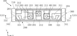
図19〜図23は、本発明の第1参考例に基づくLEDモジュールを示している。本参考例のLEDモジュール101は、基板200、配線300、3つのLEDチップ401,402,403、および透光樹脂部700を備えている。LEDモジュール101は、図23に示す姿勢でたとえば実装基板801に実装される、いわゆるサイドビュータイプのLEDモジュールとして構成されている。本参考例においては、LEDモジュール101は、x方向寸法が3.0mm程度、y方向寸法が0.43mm程度、z方向寸法が1.3mm程度とされている。
19 to 23 show an LED module based on the first reference example of the present invention. The
基板200は、たとえばガラスエポキシ樹脂からなる絶縁基板であり、x方向を長手方向、y方向を短手方向とする長矩形状であり、z方向を厚さ方向とする。基板200は、主面201、背面202、底面203、2つの側面204を有している。また、基板200には、2つの貫通孔211,212および2つのコーナー溝221,222が形成されている。図19および図22に示すように、貫通孔211,212は、y方向において底面203とは反対側寄りに配置されている。本参考例においては、基板200は、x方向寸法が3.0mm程度、y方向寸法が0.43mm程度、z方向寸法が0.5mm程度とされている。
The
2つの貫通孔211,212は、基板200をz方向に貫通しており、主面201から背面202に達している。コーナー溝221,222は、側面204と底面203との間に介在しており、z方向に延びている。コーナー溝221,222は、主面201から背面202に達しており、断面四半円形状である。
The two through
配線300は、3つのLEDチップ401,402,403に電力供給するための経路を構成するものであり、ダイボンディングパッド301,302,303、2つの四半環状部321、主面連絡配線322、枝状配線323、コーナー溝配線341,342、貫通電極351,352、および背面電極370を有している。配線300は、たとえばCuメッキ、Niメッキ、およびAuメッキが積層された構造とされている。
The
ダイボンディングパッド301,302,303は、x方向に配列されており、LEDチップ401,402,403がダイボンディングされている。ダイボンディングパッド301,302は、正方形状の部分と円形状の部分とが結合した形状とされている。ダイボンディングパッド301,302の円形状の部分どうしは、x方向において反対側に配置されている。ダイボンディングパッド303は、正方形状の部分とこれからx方向に延びる帯状部分とを有する。
The
四半環状部321は、主面201のうちコーナー溝221,222とつながる部分近傍に形成されている。主面連絡配線322は、コーナー溝221近傍にある四半環状部321からx方向に延びる帯状であり、y方向において主面201の一端寄りに配置されている。枝状配線323は、主面連絡配線322の途中部分からダイボンディングパッド301,302の間に向けてy方向に延びている。
The quaternary
コーナー溝配線341,342は、基板200のコーナー溝221,222の内面を覆うように形成されており、主面201から背面202に達している。貫通電極351,352は、貫通孔211,212の内面に形成されており、円筒形状となっている。貫通電極351,352は、主面201から背面202に達している。本参考例においては、貫通電極351,352の内側には、充填樹脂602が充填されている。
The
背面電極370は、背面202に形成されており、本参考例においては、個別電極371,372、端部個別電極374、および端部共通電極375からなる。個別電極371,372、端部個別電極374、および端部共通電極375は、x方向に並べられている。個別電極371,372は、端部個別電極374および端部共通電極375に挟まれている。個別電極371は、z方向視において貫通孔211と重なっており、貫通電極351とつながっている。個別電極372は、z方向視において貫通孔212と重なっており、貫通電極352とつながっている。端部個別電極374は、背面202の一端寄りに設けられており、コーナー溝配線342とつながっている。端部共通電極375は、背面202の他端寄りに設けられており、コーナー溝配線341とつながっている。
The
本参考例においては、背面202に複数の絶縁膜601が設けられている。これらの絶縁膜601は、背面202のうち背面電極370から露出した部分、および個別電極371,372の一部ずつを覆っている。また、底面203には、配線300は形成されておらず、底面203のすべてが露出している。LEDモジュール101を図23に示す実装基板801に実装するときには、実装基板801のパッド(図示略)と個別電極371,372とに接するハンダフィレット802が形成される。また、端部個別電極374と端部共通電極375は、ハンダフィレット802が形成されるだけでなく、ハンダフィレット802の一部が、端部個別電極374または端部共通電極375と実装基板801とに囲まれた空間に充てんされる格好となる。
In this reference example, a plurality of insulating
LEDチップ401,402,403は、LEDモジュール101の光源であり、たとえばp型半導体層、n型半導体層、およびこれらに挟まれた活性層が積層された構造とされている。LEDチップ401は、ダイボンディングパッド301にダイボンディングされており、たとえば青色光を発する。LEDチップ402は、ダイボンディングパッド302にダイボンディングされており、たとえば赤色光を発する。LEDチップ403は、ダイボンディングパッド303にダイボンディングされており、たとえば緑色光を発する。LEDチップ401,402は、各々ワイヤ500によって枝状配線323に接続されている。LEDチップ403は、ワイヤ500によって主面連絡配線322に接続されている。LEDチップ401,402,403どうしの離間距離は、100〜150μmであることが好ましい。
The LED chips 401, 402, and 403 are light sources of the
個別電極371は、貫通電極351を介してLEDチップ401と導通している。個別電極372は、貫通電極352を介してLEDチップ402と導通している。端部個別電極374は、コーナー溝配線342を介してLEDチップ403と導通している。端部共通電極375は、コーナー溝配線341を介してLEDチップ401,402,403と導通している。
The
透光樹脂部700は、基板200の主面201に設けられており、LEDチップ401,402,403を覆っている。透光樹脂部700は、たとえばエポキシ樹脂などの透明な樹脂またはLEDチップ401,402,403からの光を透過可能な樹脂からなる。本参考例においては、透光樹脂部700のy方向視形状は、台形状となっており、x方向視形状は長方形となっている。透光樹脂部700のz方向寸法は、たとえば0.8mm程度である。
The
次に、LEDモジュール101の作用について説明する。
Next, the operation of the
本参考例によれば、個別電極371,372から貫通電極351,352を介した経路が、LEDチップ401,402に電力を供給する経路として利用される。この経路は、主面201または背面202から底面203へと回り込む部分を有さない。このため、配線300を形成するため主面201および背面202に確保すべきスペースを縮小することが可能である。したがって、LEDモジュール101の小型化を図ることができる。
According to this reference example, the path from the
端部個別電極374および端部共通電極375からコーナー溝配線341,342を介した経路が、LEDチップ401,402,403に電力を供給する経路として利用される。これにより、底面203は、配線300によって全く覆われていない。すなわち、主面201または背面202から底面203へと配線300を回り込ませる部分は一切存在しない。したがって、配線300を形成するために主面201および背面202に確保すべきスペースを更に縮小することができる。
The path from the end
図22に示すように、貫通孔211,212がy方向において底面203から離間した側にある。これにより、貫通孔211,212の存在によって個別電極371,372に意図しない変形が発生したとしても、この変形によってLEDモジュール101の実装姿勢が乱されてしまうことを回避することができる。
As shown in FIG. 22, the through
図24〜図31において、上記参考例と同一または類似の要素には、上記参考例と同一の符号を付している。 In FIGS. 24 to 31, elements that are the same as or similar to those of the reference example are designated by the same reference numerals as those of the reference example.
図24〜図27は、本発明の第2参考例に基づくLEDモジュールを示している。本参考例のLEDモジュール102は、3つの貫通孔211,212,213を備えており、3つの個別電極371,372,373と2つの端部共通電極375,376を有している。また、LEDモジュール102は、リフレクタ710を備えている。LEDモジュール102は、x方向寸法が2.0mm程度、y方向寸法が0.5mm程度、z方向寸法が0.9mm程度とされている。なお、図24においては、理解の便宜上、透光樹脂部700を省略している。
24 to 27 show an LED module based on the second reference example of the present invention. The
基板200には、3つの貫通孔211,212,213が形成されている。これらの貫通孔211,212,213の内面には、貫通電極351,352,353(貫通電極351,353は図示略)が形成されている。個別電極371,372,373は、順に貫
通電極351,352,353とつながっている。主面201には、3つのダイボンディングパッド301,302,303が形成されている。3つのLEDチップ401,402,403は、ダイボンディングパッド301,302,303にダイボンディングされており、貫通電極351,352,353と導通している。貫通孔211,213(貫通電極351,353)は、LEDチップ401,403に対して図24における図中上側に配置されている。貫通孔212(貫通電極352)は、LEDチップ402に対して図24における図中下側に配置されている。
Three through holes 211,212, 213 are formed in the
主面201には、2つのボンディングパッド311,312が形成されている。ボンディングパッド311とLEDチップ401とはワイヤ500によって接続されている。ボンディングパッド312とLEDチップ402,403とは各々ワイヤ500によって接続されている。ボンディングパッド311は、一方の四半環状部321につながっており、コーナー溝配線341を介して端部共通電極375と導通している。ボンディングパッド312は、他方の四半環状部321につながっており、コーナー溝配線342を介して端部共通電極376と導通している。
Two
リフレクタ710は、たとえば白色樹脂からなり、主面201に形成されている。リフレクタ710は、反射面711を有している。反射面711は、LEDチップ401,402,403を囲んでおり、LEDチップ401,402,403からx方向またはy方向に進行してきた光をz方向に向けて反射する機能を果たす。リフレクタ710のz方向寸法は、たとえば0.4mm程度である。リフレクタ710に囲まれた領域には、透光樹脂部700が充填されている。
The
このような参考例によっても、LEDモジュール102の小型化を図ることができる。LEDチップ401,402,403と貫通孔211,212,213とをいわゆる千鳥状の配置とすることにより、基板200のx方向寸法を縮小することができる。
The
図28〜図31は、本発明の第3実施形態に基づくLEDモジュールを示している。本実施形態のLEDモジュール103は、主面201および背面202における配線300の構成が、上述したLEDモジュール102と異なっている。LEDモジュール103は、x方向寸法が2.7mm程度、y方向寸法が0.5mm程度、z方向寸法が0.9mm程度とされている。なお、図28においては、理解の便宜上、透光樹脂部700を省略している。図31においては、絶縁膜601が形成されている領域を、ハッチングを付して表している。
28 to 31 show an LED module based on the third embodiment of the present invention. The
本実施形態においては、ダイボンディングパッド303が四半環状部321につながっている。この四半環状部321は、コーナー溝配線342につながっている。背面電極370は、端部個別電極374を有している。端部個別電極374は、コーナー溝配線342につながっている。LEDチップ403に対してワイヤ500によって接続されたボンディングパッド312は、貫通孔213に形成された貫通電極353(図示略)につながっている。背面電極370は、背面連絡配線378を有している。背面連絡配線378は、貫通電極353と端部共通電極375とをつないでいる。主面201においては、ボンディングパッド311とLEDチップ401,402とが各々ワイヤ500によって接続されている。ボンディングパッド311は、コーナー溝配線341を介して端部共通電極375に導通している。これにより、端部共通電極375は、LEDチップ401,402だけでなくLEDチップ403とも導通している。貫通孔211,212は、z方向視においてLEDチップ401,402と重なっている。
In the present embodiment, the
LEDチップ402と、複数のワイヤ500のうちボンディングパッド311と、を接続するワイヤ500は、方向z視において、LEDチップ401と重なる部位を有する。LEDチップ401の中心は、LEDチップ402の中心に対し、方向yにおいて、ずれた位置に位置している。貫通孔212は、方向z視において、LEDチップ402に重なる部位と、LEDチップ402からはみ出た部位と、を有する。
The
絶縁膜601は、背面電極370を覆っている。具体的には、絶縁膜601は背面連絡配線378を覆っている。絶縁膜601は、個別電極371,372の少なくとも一部分ずつを露出させている。絶縁膜601は、個別電極371,372のうちの、背面連絡配線378に近接する部分を覆っている。このことにより、絶縁膜601がめくれてしまうことを防止できる。絶縁膜601は、端部個別電極374および端部共通電極375のいずれをも露出させている。
The insulating
このような実施形態によっても、LEDモジュール103の小型化を図ることができる。貫通孔211,212をz方向視においてLEDチップ401,402と重ねることにより、基板200の小型化、すなわちLEDモジュール103の小型化を更に促進することができる。
The
LEDモジュール103においては、LEDチップ402と、複数のワイヤ500のうちボンディングパッド311と、を接続するワイヤ500は、方向z視において、LEDチップ401と重なる部位を有する。このような構成によると、LEDチップ401の互いに反対側に配置されたLEDチップ402およびボンディングパッド311に、ワイヤ500を接合することができる。したがって、LEDチップ402とLEDチップ401との間や、LEDチップ402とLEDチップ403との間に、LEDチップ402に接合されたワイヤ500をボンディングするためのボンディングパッドを形成する必要がない。よって、LEDチップ402とLEDチップ401との離間距離、もしくは、LEDチップ402とLEDチップ403との離間距離、を小さくすることができる。
In the
LEDモジュール103においては、LEDチップ401の中心は、LEDチップ402の中心に対し、方向yにおいて、ずれた位置に位置している。これは、LEDチップ401に接続するワイヤ500と、LEDチップ402に接続するワイヤ500とが接触することを防止するのに好適である。また、ワイヤ500を形成する際に用いるキャピラリが、他のワイヤ500に接触することを防止するにも好適である。
In the
LEDモジュール103においては、貫通孔212は、方向z視において、LEDチップ402に重なる部位と、LEDチップ402からはみ出た部位と、を有する。このような構成によると、貫通孔212に重なる個別電極372と、背面連絡配線378と、の離間距離をある程度離間させることができる。
In the
LEDモジュール103においては、絶縁膜601は背面連絡配線378を覆っている。このような構成によると、個別電極371や個別電極372に接するハンダが、背面連絡配線378に付着することを防止できる。よって、個別電極371や個別電極372がハンダを介し背面連絡配線378とショートする不具合を防止できる。
In the
本発明は、上述した実施形態に限定されるものではない。本発明の各部の具体的な構成は、種々に設計変更自在である。 The present invention is not limited to the above-described embodiments. The specific configuration of each part of the present invention can be freely redesigned.
B1 実装構造
871 実装基板
872 ハンダ層
A1,A2 LEDモジュール
1,1’ 基板
11 主面
12 基板側面
13 裏面
15 露出部
17 端縁
2 主面電極
24 第1導電部
241,241a,241b,241c ダイパッド
242,242a,242b,242c ワイヤボンディングパッド
243,243a,243b,243c 円形パッド
244,245,244a,244b,244c 帯状部
25 第2導電部
251 ワイヤボンディング配線部
252 円形配線部
31 貫通電極
4 裏面電極
41 実装パッド部
511,512,513 LEDチップ
521,522,523 接合層
59 封止樹脂部
6,6’ ケース
61 包囲面
62 ケース側面
63 底面
71 接着層
74 絶縁膜
741 第1帯状絶縁部
742 第2帯状絶縁部
81 ワイヤ
881 中間品
882 ステージ
891 第1金型
892 第2金型
895 ダイシングブレード
101,102,103 LEDモジュール
200 基板
201 主面
202 背面
203 底面
204 側面
211,212,213 貫通孔
221,222 コーナー溝
300 配線
301,302,303 ダイボンディングパッド(パッド)
311,312 ボンディングパッド(パッド)
321 四半環状部
322 主面連絡配線
323 枝状配線
341,342 コーナー溝配線
351,352,353 貫通電極
370 背面電極
371,372,373 個別電極
374 端部個別電極
375,376 端部共通電極
378 背面連絡配線
401,402,403 LEDチップ
500 ワイヤ
601 絶縁膜
602 充填樹脂
700 透光樹脂部
710 リフレクタ
711 反射面
801 実装基板
802 ハンダフィレット
311, 312 Bonding pad (pad)
321
Claims (6)
前記主面に形成された主面電極と、
前記主面電極に前記厚さ方向と直角である第1方向に沿って一方側から他方側に順に配列された第1LEDチップ、第2LEDチップおよび第3LEDチップと、
前記第1LEDチップと前記主面電極とにボンディングされた第1ワイヤと、
前記第2LEDチップと前記主面電極とにボンディングされた第2ワイヤと、
前記第3LEDチップと前記主面電極とにボンディングされた第3ワイヤと、
前記主面に配置され且つ前記第1ないし前記第3LEDチップを囲むケースと、を備え、
前記主面電極は、第1導電部を含み、
前記第1導電部は、第1ダイパッドと、前記第1ダイパッドに導通している第1ワイヤボンディングパッドと、を有し、
前記第1ダイパッドと前記第1ワイヤボンディングパッドとは、隙間を介して前記厚さ方向および前記第1方向と直角である第2方向に離間して配置されており、
前記第1ダイパッドには、前記第1ないし前記第3LEDチップが配置され、
前記第1ワイヤボンディングパッドには、前記第2ワイヤおよび前記第3ワイヤがボンディングされており、
前記主面電極は、前記第1導電部から絶縁された第2導電部をさらに含み、
前記第2導電部は、前記第1ワイヤボンディングパッドに対して前記第1方向一方側に配置されており、且つ前記第1ワイヤがボンディングされており、
前記第1ワイヤボンディングパッドは、第1ダイパッドのうち前記厚さ方向視において前記第1LEDチップおよび前記第2LEDチップに重なる部分と前記第2方向視において重なり、且つ前記第1ダイパッドのうち前記厚さ方向視において前記第3LEDチップに重なる部分と前記第2方向視において離間しており、
前記第2導電部は、前記第1ダイパッドのうち前記厚さ方向視において前記第1LEDチップに重なる部分と前記第2方向視において重なり、且つ前記第1ダイパッドのうち前記厚さ方向視において前記第2LEDチップおよび前記第3LEDチップに重なる部分と前記第2方向視において離間しており、
前記主面電極につながり且つ前記基板を貫通する複数の貫通電極と、
前記裏面に形成され且つ前記複数の貫通電極の各々につながる裏面電極と、をさらに備え、
前記第1導電部は、前記第1ダイパッドおよび前記第1ワイヤボンディングパッドの間に介在する円形の円形パッドをさらに有し、
前記円形パッドは、前記複数の貫通電極のいずれかとつながり、
前記円形パッドにつながる前記貫通電極は、平面視において前記円形パッドに内包されており、
前記円形パッドは、前記第1ダイパッドに対して前記第2方向に配置されており、且つ前記第1ワイヤボンディングパッドに対して前記第1方向他方側に配置されており、
前記第1導電部は、前記第1ダイパッドと前記円形パッドとをつなぐ第1帯状部と、前記円形パッドと前記第1ワイヤボンディングパッドとをつなぐ第2帯状部と、をさらに有し、
前記第1ワイヤボンディングパッドの前記第2方向の大きさは、前記第2帯状部の前記第2方向の大きさよりも大きく、
前記主面電極は、前記厚さ方向に視て前記主面の外端縁よりも内側に配置されており、
前記ケースは、前記厚さ方向に視て前記主面の外端縁に到達している、LEDモジュール。 A substrate having a main surface and a back surface facing opposite sides in the thickness direction,
With the main surface electrodes formed on the main surface,
The first LED chip, the second LED chip, and the third LED chip arranged in order from one side to the other side along the first direction perpendicular to the thickness direction on the main surface electrode.
A first wire bonded to the first LED chip and the main surface electrode,
A second wire bonded to the second LED chip and the main surface electrode,
A third wire bonded to the third LED chip and the main surface electrode,
A case arranged on the main surface and surrounding the first to third LED chips is provided.
The main surface electrode includes a first conductive portion and includes a first conductive portion.
The first conductive portion includes a first die pad and a first wire bonding pad conducting the first die pad.
The first die pad and the first wire bonding pad are arranged apart from each other through a gap in the thickness direction and the second direction perpendicular to the first direction.
The first to third LED chips are arranged on the first die pad.
The second wire and the third wire are bonded to the first wire bonding pad.
The main surface electrode further includes a second conductive portion insulated from the first conductive portion.
The second conductive portion is arranged on one side of the first direction with respect to the first wire bonding pad, and the first wire is bonded.
The first wire bonding pad overlaps the portion of the first die pad that overlaps the first LED chip and the second LED chip in the thickness direction, and is the thickness of the first die pad that overlaps in the second direction. The portion overlapping the third LED chip in the directional view and the portion overlapping the third LED chip in the directional view are separated from each other in the second directional view.
The second conductive portion overlaps the portion of the first die pad that overlaps with the first LED chip in the thickness direction view and overlaps with the portion of the first die pad that overlaps with the first LED chip in the thickness direction view, and the first die pad of the first die pad that overlaps with the thickness direction view. It is separated from the portion overlapping the 2LED chip and the 3rd LED chip in the 2nd direction view.
A plurality of through electrodes connected to the main surface electrode and penetrating the substrate,
A back surface electrode formed on the back surface and connected to each of the plurality of through electrodes is further provided.
The first conductive portion further has a circular circular pad interposed between the first die pad and the first wire bonding pad.
The circular pad is connected to any of the plurality of through electrodes,
The through electrode connected to the circular pad is included in the circular pad in a plan view.
The circular pad is arranged in the second direction with respect to the first die pad, and is arranged on the other side of the first direction with respect to the first wire bonding pad.
The first conductive portion further includes a first strip-shaped portion connecting the first die pad and the circular pad, and a second strip-shaped portion connecting the circular pad and the first wire bonding pad.
The size of the first wire bonding pad in the second direction is larger than the size of the second band-shaped portion in the second direction.
The main surface electrodes are arranged inside the outer edge of the main surface when viewed in the thickness direction.
The case is an LED module that reaches the outer edge of the main surface when viewed in the thickness direction.
前記第2ワイヤボンディング配線部に、前記第1ワイヤがボンディングされており、
前記第2円形配線部に、前記複数の貫通電極のいずれかが繋がり、
前記第2円形配線部につながる前記貫通電極は、平面視において前記第2円形配線部に内包されている、請求項1ないし3のいずれかに記載のLEDモジュール。 The second conductive portion has a second wire bonding wiring portion and a circular second circular wiring portion.
The first wire is bonded to the second wire bonding wiring portion.
One of the plurality of through electrodes is connected to the second circular wiring portion,
The LED module according to any one of claims 1 to 3 , wherein the through electrode connected to the second circular wiring portion is included in the second circular wiring portion in a plan view.
前記第3導電部は、前記第2方向において前記第1ダイパッドを挟んで前記第1ワイヤボンディングパッドとは反対側に配置されており、
前記第2LEDチップと前記第3導電部とにボンディングされた追加の第2ワイヤを備える、請求項1ないし4のいずれかに記載のLEDモジュール。 The main surface electrode further includes a third conductive portion insulated from the first conductive portion.
The third conductive portion is arranged on the side opposite to the first wire bonding pad with the first die pad sandwiched in the second direction.
The LED module according to any one of claims 1 to 4 , further comprising an additional second wire bonded to the second LED chip and the third conductive portion.
前記第4導電部は、前記第2方向において前記第1ダイパッドを挟んで前記第1ワイヤボンディングパッドとは反対側に配置されているとともに前記第3導電部に対して前記第1方向他方側に配置されており、
前記第3LEDチップと前記第4導電部とにボンディングされた追加の第3ワイヤを備える、請求項5に記載のLEDモジュール。 The main surface electrode further includes a fourth conductive portion insulated from the first conductive portion.
The fourth conductive portion is arranged on the side opposite to the first wire bonding pad with the first die pad sandwiched in the second direction, and on the other side of the first direction with respect to the third conductive portion. Have been placed and
The LED module according to claim 5 , further comprising an additional third wire bonded to the third LED chip and the fourth conductive portion.
Priority Applications (1)
| Application Number | Priority Date | Filing Date | Title |
|---|---|---|---|
| JP2019038818A JP6842485B2 (en) | 2019-03-04 | 2019-03-04 | LED module |
Applications Claiming Priority (1)
| Application Number | Priority Date | Filing Date | Title |
|---|---|---|---|
| JP2019038818A JP6842485B2 (en) | 2019-03-04 | 2019-03-04 | LED module |
Related Parent Applications (1)
| Application Number | Title | Priority Date | Filing Date |
|---|---|---|---|
| JP2017102329A Division JP2017143314A (en) | 2017-05-24 | 2017-05-24 | LED module |
Publications (2)
| Publication Number | Publication Date |
|---|---|
| JP2019083350A JP2019083350A (en) | 2019-05-30 |
| JP6842485B2 true JP6842485B2 (en) | 2021-03-17 |
Family
ID=66670599
Family Applications (1)
| Application Number | Title | Priority Date | Filing Date |
|---|---|---|---|
| JP2019038818A Active JP6842485B2 (en) | 2019-03-04 | 2019-03-04 | LED module |
Country Status (1)
| Country | Link |
|---|---|
| JP (1) | JP6842485B2 (en) |
Families Citing this family (1)
| Publication number | Priority date | Publication date | Assignee | Title |
|---|---|---|---|---|
| CN114335310A (en) * | 2021-11-30 | 2022-04-12 | 佛山市国星光电股份有限公司 | LED device |
Family Cites Families (19)
| Publication number | Priority date | Publication date | Assignee | Title |
|---|---|---|---|---|
| JP3217322B2 (en) * | 1999-02-18 | 2001-10-09 | 日亜化学工業株式会社 | Chip component type light emitting device |
| JP2001177156A (en) * | 1999-12-14 | 2001-06-29 | Koha Co Ltd | Side emitting led lamp |
| JP2001345485A (en) * | 2000-06-02 | 2001-12-14 | Toyoda Gosei Co Ltd | Light emitting device |
| JP2002314143A (en) * | 2001-04-09 | 2002-10-25 | Toshiba Corp | Light emitting device |
| JP2002314138A (en) * | 2001-04-09 | 2002-10-25 | Toshiba Corp | Light emitting device |
| JP4239509B2 (en) * | 2002-08-02 | 2009-03-18 | 日亜化学工業株式会社 | Light emitting diode |
| JP4306247B2 (en) * | 2002-12-27 | 2009-07-29 | 日亜化学工業株式会社 | Semiconductor light emitting device |
| JP4830768B2 (en) * | 2006-05-10 | 2011-12-07 | 日亜化学工業株式会社 | Semiconductor light emitting device and method for manufacturing semiconductor light emitting device |
| JP5057707B2 (en) * | 2006-06-16 | 2012-10-24 | 日亜化学工業株式会社 | Light emitting device |
| JP4858032B2 (en) * | 2006-09-15 | 2012-01-18 | 日亜化学工業株式会社 | Light emitting device |
| JP4306772B2 (en) * | 2006-10-05 | 2009-08-05 | 日亜化学工業株式会社 | Light emitting device |
| JP4983348B2 (en) * | 2007-04-04 | 2012-07-25 | 豊田合成株式会社 | Light emitting device |
| JP5453713B2 (en) * | 2007-07-06 | 2014-03-26 | 日亜化学工業株式会社 | Semiconductor device and method for forming the same |
| CN101388161A (en) * | 2007-09-14 | 2009-03-18 | 科锐香港有限公司 | LED surface mounting device and LED display with the device |
| JP5132404B2 (en) * | 2008-04-17 | 2013-01-30 | スタンレー電気株式会社 | Semiconductor light emitting device |
| JP2009277705A (en) * | 2008-05-12 | 2009-11-26 | Koa Corp | Package light-emitting component and method of manufacturing the same |
| US8049230B2 (en) * | 2008-05-16 | 2011-11-01 | Cree Huizhou Opto Limited | Apparatus and system for miniature surface mount devices |
| JP5392059B2 (en) * | 2009-12-24 | 2014-01-22 | 日亜化学工業株式会社 | Semiconductor device |
| JP2013026510A (en) * | 2011-07-22 | 2013-02-04 | Rohm Co Ltd | Led module and mounting structure of the same |
-
2019
- 2019-03-04 JP JP2019038818A patent/JP6842485B2/en active Active
Also Published As
| Publication number | Publication date |
|---|---|
| JP2019083350A (en) | 2019-05-30 |
Similar Documents
| Publication | Publication Date | Title |
|---|---|---|
| JP2013026510A (en) | Led module and mounting structure of the same | |
| US10950759B2 (en) | LED module | |
| US10593846B2 (en) | Semiconductor light-emitting device, method for producing same, and display device | |
| US10103130B2 (en) | LED module | |
| US9847282B2 (en) | Semiconductor device | |
| US10381331B2 (en) | Semiconductor light-emitting device | |
| US9583455B2 (en) | Semiconductor device | |
| US10153258B2 (en) | LED package | |
| US20130043501A1 (en) | Led module | |
| US20130049058A1 (en) | Led module | |
| US9543279B2 (en) | Method of manufacturing a single light-emitting structure | |
| JP6842485B2 (en) | LED module | |
| JP2004288937A (en) | Package for accommodating light emitting element and light emitting device | |
| JP6450096B2 (en) | Optical device, semiconductor device, mounting structure of optical device, and manufacturing method of optical device | |
| JP2017143314A (en) | LED module | |
| JP5913432B2 (en) | Chip light emitting device | |
| JP5436353B2 (en) | Light emitting device | |
| JP7089343B2 (en) | Semiconductor light emitting device | |
| JP2017157683A (en) | Led light-emitting device and manufacturing method thereof | |
| JP2018142708A (en) | Led module and packaging structure of the same | |
| JP2024039359A (en) | Semiconductor device and its manufacturing method | |
| JP2019186583A (en) | Light-emitting device |
Legal Events
| Date | Code | Title | Description |
|---|---|---|---|
| A621 | Written request for application examination |
Free format text: JAPANESE INTERMEDIATE CODE: A621 Effective date: 20190307 |
|
| A977 | Report on retrieval |
Free format text: JAPANESE INTERMEDIATE CODE: A971007 Effective date: 20200128 |
|
| A131 | Notification of reasons for refusal |
Free format text: JAPANESE INTERMEDIATE CODE: A131 Effective date: 20200204 |
|
| A521 | Request for written amendment filed |
Free format text: JAPANESE INTERMEDIATE CODE: A523 Effective date: 20200403 |
|
| A131 | Notification of reasons for refusal |
Free format text: JAPANESE INTERMEDIATE CODE: A131 Effective date: 20200929 |
|
| A521 | Request for written amendment filed |
Free format text: JAPANESE INTERMEDIATE CODE: A523 Effective date: 20201030 |
|
| TRDD | Decision of grant or rejection written | ||
| A01 | Written decision to grant a patent or to grant a registration (utility model) |
Free format text: JAPANESE INTERMEDIATE CODE: A01 Effective date: 20210202 |
|
| A61 | First payment of annual fees (during grant procedure) |
Free format text: JAPANESE INTERMEDIATE CODE: A61 Effective date: 20210219 |
|
| R150 | Certificate of patent or registration of utility model |
Ref document number: 6842485 Country of ref document: JP Free format text: JAPANESE INTERMEDIATE CODE: R150 |
|
| R250 | Receipt of annual fees |
Free format text: JAPANESE INTERMEDIATE CODE: R250 |