JP6834091B2 - Multilayer ceramic electronic components and their manufacturing methods - Google Patents
Multilayer ceramic electronic components and their manufacturing methods Download PDFInfo
- Publication number
- JP6834091B2 JP6834091B2 JP2016143778A JP2016143778A JP6834091B2 JP 6834091 B2 JP6834091 B2 JP 6834091B2 JP 2016143778 A JP2016143778 A JP 2016143778A JP 2016143778 A JP2016143778 A JP 2016143778A JP 6834091 B2 JP6834091 B2 JP 6834091B2
- Authority
- JP
- Japan
- Prior art keywords
- ceramic
- internal electrode
- laminated
- dielectric layer
- region
- Prior art date
- Legal status (The legal status is an assumption and is not a legal conclusion. Google has not performed a legal analysis and makes no representation as to the accuracy of the status listed.)
- Active
Links
Images


Classifications
-
- H—ELECTRICITY
- H01—ELECTRIC ELEMENTS
- H01G—CAPACITORS; CAPACITORS, RECTIFIERS, DETECTORS, SWITCHING DEVICES, LIGHT-SENSITIVE OR TEMPERATURE-SENSITIVE DEVICES OF THE ELECTROLYTIC TYPE
- H01G4/00—Fixed capacitors; Processes of their manufacture
- H01G4/30—Stacked capacitors
- H01G4/308—Stacked capacitors made by transfer techniques
-
- H—ELECTRICITY
- H01—ELECTRIC ELEMENTS
- H01G—CAPACITORS; CAPACITORS, RECTIFIERS, DETECTORS, SWITCHING DEVICES, LIGHT-SENSITIVE OR TEMPERATURE-SENSITIVE DEVICES OF THE ELECTROLYTIC TYPE
- H01G13/00—Apparatus specially adapted for manufacturing capacitors; Processes specially adapted for manufacturing capacitors not provided for in groups H01G4/00 - H01G11/00
-
- H—ELECTRICITY
- H01—ELECTRIC ELEMENTS
- H01G—CAPACITORS; CAPACITORS, RECTIFIERS, DETECTORS, SWITCHING DEVICES, LIGHT-SENSITIVE OR TEMPERATURE-SENSITIVE DEVICES OF THE ELECTROLYTIC TYPE
- H01G4/00—Fixed capacitors; Processes of their manufacture
- H01G4/002—Details
- H01G4/005—Electrodes
- H01G4/012—Form of non-self-supporting electrodes
-
- H—ELECTRICITY
- H01—ELECTRIC ELEMENTS
- H01G—CAPACITORS; CAPACITORS, RECTIFIERS, DETECTORS, SWITCHING DEVICES, LIGHT-SENSITIVE OR TEMPERATURE-SENSITIVE DEVICES OF THE ELECTROLYTIC TYPE
- H01G4/00—Fixed capacitors; Processes of their manufacture
- H01G4/002—Details
- H01G4/228—Terminals
- H01G4/232—Terminals electrically connecting two or more layers of a stacked or rolled capacitor
-
- H—ELECTRICITY
- H01—ELECTRIC ELEMENTS
- H01G—CAPACITORS; CAPACITORS, RECTIFIERS, DETECTORS, SWITCHING DEVICES, LIGHT-SENSITIVE OR TEMPERATURE-SENSITIVE DEVICES OF THE ELECTROLYTIC TYPE
- H01G4/00—Fixed capacitors; Processes of their manufacture
- H01G4/30—Stacked capacitors
-
- H—ELECTRICITY
- H01—ELECTRIC ELEMENTS
- H01G—CAPACITORS; CAPACITORS, RECTIFIERS, DETECTORS, SWITCHING DEVICES, LIGHT-SENSITIVE OR TEMPERATURE-SENSITIVE DEVICES OF THE ELECTROLYTIC TYPE
- H01G4/00—Fixed capacitors; Processes of their manufacture
- H01G4/002—Details
- H01G4/018—Dielectrics
- H01G4/06—Solid dielectrics
- H01G4/08—Inorganic dielectrics
- H01G4/12—Ceramic dielectrics
- H01G4/1209—Ceramic dielectrics characterised by the ceramic dielectric material
- H01G4/1218—Ceramic dielectrics characterised by the ceramic dielectric material based on titanium oxides or titanates
- H01G4/1227—Ceramic dielectrics characterised by the ceramic dielectric material based on titanium oxides or titanates based on alkaline earth titanates
Landscapes
- Engineering & Computer Science (AREA)
- Power Engineering (AREA)
- Manufacturing & Machinery (AREA)
- Microelectronics & Electronic Packaging (AREA)
- Ceramic Engineering (AREA)
- Chemical & Material Sciences (AREA)
- Inorganic Chemistry (AREA)
- Fixed Capacitors And Capacitor Manufacturing Machines (AREA)
- Ceramic Capacitors (AREA)
Description
本発明は、高容量積層セラミック電子部品において、部品内部の段差を改善して耐電圧特性を向上させた積層セラミック電子部品及びその製造方法に関する。 The present invention relates to a laminated ceramic electronic component having improved withstand voltage characteristics by improving a step inside the component and a method for manufacturing the same in a high-capacity laminated ceramic electronic component.
積層セラミック電子部品は、積層された複数の誘電体層と、一誘電体層を挟んで対向配置される内部電極と、上記内部電極に電気的に接続された外部電極と、を含む。 The laminated ceramic electronic component includes a plurality of laminated dielectric layers, an internal electrode arranged so as to face each other with the one dielectric layer interposed therebetween, and an external electrode electrically connected to the internal electrode.
積層セラミック電子部品は、小型でありながら高容量が保証され、実装が容易であるという利点から、コンピューター、PDA、携帯電話などの移動通信装置の部品として広く使用されている。 Multilayer ceramic electronic components are widely used as components for mobile communication devices such as computers, PDAs, and mobile phones because of their advantages of being small, guaranteed high capacity, and easy to mount.
近年、電子製品の小型化及び多機能化に伴い、チップ部品もまた小型化及び高機能化する傾向にあり、積層セラミック電子部品もそのサイズが小さく、且つ容量が大きい高容量の製品が求められている。 In recent years, as electronic products have become smaller and more multifunctional, chip components have also tended to become smaller and more sophisticated, and multilayer ceramic electronic components are also required to have high capacity products having a small size and a large capacity. ing.
一般的に、積層セラミック電子部品の製造方法は、セラミックグリーンシートを製造し、セラミックグリーンシート上に導電性ペーストを印刷して内部電極膜を形成する。内部電極膜が形成されたセラミックグリーンシートを数十層から数百層まで重ねて積み上げ、グリーンセラミック本体を作製する。 Generally, a method for manufacturing a laminated ceramic electronic component is to manufacture a ceramic green sheet and print a conductive paste on the ceramic green sheet to form an internal electrode film. A ceramic green sheet on which an internal electrode film is formed is stacked from tens to hundreds of layers to prepare a green ceramic body.
次に、グリーンセラミック本体を高温及び高圧で圧着し、強固なグリーンセラミック本体を作製し、切断工程を経た後、仮焼、焼成、研磨を行い、外部電極を形成して積層セラミックキャパシターを完成する。 Next, the green ceramic body is crimped at high temperature and high pressure to prepare a strong green ceramic body, and after undergoing a cutting process, calcining, firing, and polishing are performed to form an external electrode to complete a laminated ceramic capacitor. ..
近年、積層されるセラミックグリーンシートの数が増加するに伴い、セラミックグリーンシートの積層工程と圧着工程を行う間に製品の信頼性に影響を及ぼすという問題点が発生している。 In recent years, as the number of ceramic green sheets to be laminated has increased, there has been a problem that the reliability of the product is affected during the laminating process and the crimping process of the ceramic green sheets.
すなわち、セラミックグリーンシートは、内部電極形成部と内部電極非形成部であるマージン部とからなり、セラミックグリーンシートが積層された後、所定の圧力が印加されて互いに圧着される場合、内部電極形成部と内部電極非形成部であるマージン部との段差が激しくなり、耐電圧特性が低下するという問題がある。 That is, the ceramic green sheet is composed of an internal electrode forming portion and a margin portion which is an internal electrode non-forming portion, and when the ceramic green sheet is laminated and then a predetermined pressure is applied to crimp each other, the internal electrode is formed. There is a problem that the step between the portion and the margin portion, which is the non-formed portion of the internal electrode, becomes large and the withstand voltage characteristic deteriorates.
上記段差は、内部電極形成部での内部電極と誘電体層の密度と、内部電極非形成部であるマージン部でのその密度との差によって発生する。 The step is generated by the difference between the density of the internal electrode and the dielectric layer in the internal electrode forming portion and the density in the margin portion which is the internal electrode non-forming portion.
上記のような段差の問題を改善するために、セラミック本体のマージン部に別のセラミック材料をネガティブ印刷(Negative Printing)工程により追加する技術があるが、この場合、セラミックグリーンシートで内部電極非形成部であるマージン部に別のセラミックスラリーを印刷する工程が非常に困難であるという問題がある。 In order to improve the problem of the step as described above, there is a technique of adding another ceramic material to the margin portion of the ceramic body by a negative printing (Negative Printing) process. In this case, the internal electrode is not formed by the ceramic green sheet. There is a problem that the process of printing another ceramic slurry on the margin portion, which is a portion, is very difficult.
また、マージン部に別のセラミック材料をネガティブ印刷(Negative Printing)工程により追加する方法は、精度が高くなく、積層後のセラミックグリーンシートの整列(Alignment)不良の問題によって段差改善の効果が十分でない。 Further, the method of adding another ceramic material to the margin portion by the negative printing (Negative Printing) process is not highly accurate, and the effect of improving the step is not sufficient due to the problem of poor alignment of the ceramic green sheet after lamination. ..
本発明は、上記問題点を解決するためのものであり、本発明の一実施例によると、高容量積層セラミック電子部品において、部品内部の段差を改善して耐電圧特性を向上させた積層セラミック電子部品及びその製造方法に関する。 The present invention is for solving the above problems, and according to an embodiment of the present invention, in a high-capacity laminated ceramic electronic component, a laminated ceramic in which a step inside the component is improved to improve withstand voltage characteristics. Regarding electronic parts and their manufacturing methods.
本発明の一実施形態は、誘電体層と第1内部電極及び第2内部電極が交互に積層され、且つ静電容量の形成に寄与するアクティブ領域、及び上記アクティブ領域の上下面のうち少なくとも一面に提供される保護層を含むセラミック本体と、上記第1内部電極及び第2内部電極と電気的に連結され、上記セラミック本体の両端に形成される第1外部電極及び第2外部電極と、を含み、上記アクティブ領域内には、上記セラミック本体の長さ方向の両側端部及び幅方向の両側端部のうち少なくとも一つ以上に段差吸収層が配置され、上記段差吸収層が配置された領域の側部に配置された誘電体層の厚さは、他の領域に配置された誘電体層の厚さより厚い積層セラミック電子部品を提供する。 In one embodiment of the present invention, the dielectric layer, the first internal electrode, and the second internal electrode are alternately laminated, and the active region contributes to the formation of the capacitance, and at least one surface of the upper and lower surfaces of the active region. A ceramic body including a protective layer provided in the above, and a first external electrode and a second external electrode electrically connected to the first internal electrode and the second internal electrode and formed at both ends of the ceramic body. In the active region, a step absorbing layer is arranged at least one of both side ends in the length direction and both side ends in the width direction of the ceramic body, and the step absorbing layer is arranged in the region. The thickness of the dielectric layer arranged on the side of the is thicker than the thickness of the dielectric layer arranged in other regions provides a laminated ceramic electronic component.
本発明の他の実施形態は、誘電体層と内部電極が交互に積層され、且つ静電容量の形成に寄与するアクティブ領域、及び上記アクティブ領域の上下面のうち少なくとも一面に提供される保護層を含むセラミック本体と、上記内部電極と電気的に連結され、上記セラミック本体の両端に形成される外部電極と、を含み、上記アクティブ領域の両側端部には、少なくとも一つ以上のギャップ部が配置され、上記ギャップ部に隣接した二つの内部電極の間の距離は、他の二つの内部電極の間の距離より大きい積層セラミック電子部品を提供する。 In another embodiment of the present invention, a dielectric layer and an internal electrode are alternately laminated, and an active region contributing to the formation of capacitance and a protective layer provided on at least one of the upper and lower surfaces of the active region. A ceramic body including the above, and an external electrode electrically connected to the internal electrode and formed at both ends of the ceramic body, and at least one or more gap portions are provided at both end portions of the active region. The distance between the two internal electrodes arranged and adjacent to the gap provides a laminated ceramic electronic component that is greater than the distance between the other two internal electrodes.
本発明の他の実施形態は、誘電体層と内部電極が交互に積層され、且つ静電容量の形成に寄与するアクティブ領域、及び上記アクティブ領域の上下面のうち少なくとも一面に提供される保護層を含むセラミック本体と、上記内部電極と電気的に連結され、上記セラミック本体の両端に形成される外部電極と、を含み、上記アクティブ領域の両側端部には、少なくとも一つ以上のギャップ部が配置され、上記ギャップ部に隣接した二つの内部電極は、上記内部電極の積層方向において、上記ギャップ部から離れる方向に曲がる積層セラミック電子部品を提供する。 In another embodiment of the present invention, a dielectric layer and an internal electrode are alternately laminated, and an active region contributing to the formation of capacitance and a protective layer provided on at least one of the upper and lower surfaces of the active region. A ceramic body including the above, and an external electrode electrically connected to the internal electrode and formed at both ends of the ceramic body, and at least one or more gap portions are provided at both end portions of the active region. The two internal electrodes arranged and adjacent to the gap provide a laminated ceramic electronic component that bends away from the gap in the stacking direction of the internal electrodes.
本発明の他の実施形態は、第1及び第2セラミックグリーンシートを製造する段階と、上記第1セラミックグリーンシート上に導電性金属ペーストを用いて内部電極パターンを形成する段階と、上記第2セラミックグリーンシートの長さ方向の両側端部及び幅方向の両側端部のうち少なくとも一つ以上にセラミック部材を形成して、段差吸収層を形成する段階と、上記第1及び第2セラミックグリーンシートを積層して、誘電体層と第1内部電極及び第2内部電極を含むセラミック本体を形成する段階と、上記第1内部電極及び第2内部電極と電気的に連結される第1外部電極及び第2外部電極を形成する段階と、を含み、上記セラミック本体は、静電容量の形成に寄与するアクティブ領域、及び上記アクティブ領域の上下面のうち少なくとも一面に提供される保護層を含み、上記アクティブ領域は、少なくとも2層以上の第1セラミックグリーンシートを積層し、その上部に第2セラミックグリーンシートを積層する段階を繰り返すことにより形成される積層セラミック電子部品の製造方法を提供する。 Other embodiments of the present invention include a step of producing the first and second ceramic green sheets, a step of forming an internal electrode pattern on the first ceramic green sheet using a conductive metal paste, and the second step. A step of forming a step absorbing layer by forming a ceramic member at least one of both side ends in the length direction and both side ends in the width direction of the ceramic green sheet, and the first and second ceramic green sheets. To form a ceramic body including a dielectric layer and a first internal electrode and a second internal electrode, and a first external electrode electrically connected to the first internal electrode and the second internal electrode. The ceramic body includes a step of forming a second external electrode, an active region that contributes to the formation of capacitance, and a protective layer provided on at least one of the upper and lower surfaces of the active region. The active region provides a method for manufacturing a laminated ceramic electronic component formed by laminating at least two or more layers of a first ceramic green sheet and repeating a step of laminating a second ceramic green sheet on the first ceramic green sheet.
本発明の他の実施形態は、誘電体層を介して交互に配置された第1内部電極及び第2内部電極、及び幅方向の両側に延びたマージン部内に配置された段差吸収層を含むセラミック本体と、上記第1内部電極及び第2内部電極と電気的に連結され、上記セラミック本体の両端に形成される第1外部電極及び第2外部電極と、を含み、上記段差吸収層は、上記セラミック本体の一端面において上記第1内部電極の上部に配置され、他端面において上記第2内部電極の下部に配置される積層セラミック電子部品を提供する。 Another embodiment of the present invention is a ceramic including a first internal electrode and a second internal electrode arranged alternately via a dielectric layer, and a step absorbing layer arranged in a margin portion extending on both sides in the width direction. The step absorbing layer includes a first external electrode and a second external electrode that are electrically connected to the main body and the first internal electrode and the second internal electrode and are formed at both ends of the ceramic main body. Provided is a laminated ceramic electronic component that is arranged on one end surface of a ceramic body above the first internal electrode and below the second internal electrode on the other end surface.
本発明の他の実施形態は、マージン部によって一面以上に離れて第1セラミックグリーンシート上に内部電極パターンを形成する段階と、上記第1セラミックグリーンシートのマージン部に対応する第2セラミックグリーンシートの領域上にセラミック部材を形成する段階と、複数の第1セラミックグリーンシート上に上記第2セラミックグリーンシートのうち一つ以上を積層する段階と、を含む積層セラミック電子部品の製造方法を提供する。 In another embodiment of the present invention, there is a step of forming an internal electrode pattern on the first ceramic green sheet separated by one or more surfaces by a margin portion, and a second ceramic green sheet corresponding to the margin portion of the first ceramic green sheet. Provided is a method for manufacturing a laminated ceramic electronic component including a step of forming a ceramic member on the region of the above and a step of laminating one or more of the second ceramic green sheets on a plurality of first ceramic green sheets. ..
本発明によると、静電容量の形成に寄与するアクティブ領域において、マージン部に段差吸収層が配置された少なくとも一つ以上の別の誘電体層を配置することにより、段差の問題を改善して耐電圧特性が向上した高容量積層セラミック電子部品を実現することができる。 According to the present invention, in the active region that contributes to the formation of the capacitance, the problem of the step is improved by arranging at least one other dielectric layer in which the step absorbing layer is arranged in the margin portion. It is possible to realize a high-capacitance laminated ceramic electronic component with improved withstand voltage characteristics.
以下では、添付の図面を参照して本発明の好ましい実施形態について説明する。しかし、本発明の実形態は様々な他の形態に変形されることができ、本発明の範囲は以下で説明する実施形態に限定されない。また、本発明の実施形態は、当該技術分野で平均的な知識を有する者に本発明をより完全に説明するために提供されるものである。したがって、図面における要素の形状及び大きさなどはより明確な説明のために誇張されることがある。 Hereinafter, preferred embodiments of the present invention will be described with reference to the accompanying drawings. However, the actual embodiment of the present invention can be transformed into various other forms, and the scope of the present invention is not limited to the embodiments described below. In addition, embodiments of the present invention are provided to more fully explain the present invention to those having average knowledge in the art. Therefore, the shape and size of the elements in the drawings may be exaggerated for a clearer explanation.
以下、添付の図面を参照して、本発明の好ましい実施形態に係る積層セラミック電子部品について説明するに際し、特に積層セラミックキャパシターについて説明するが、これに制限されるものではない。 Hereinafter, when the laminated ceramic electronic component according to the preferred embodiment of the present invention is described with reference to the accompanying drawings, the laminated ceramic capacitor will be particularly described, but the present invention is not limited thereto.
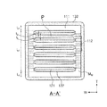
図1は本発明の一実施形態に係る積層セラミックキャパシターを概略的に示す斜視図であり、図2は図1のA−A'線に沿った断面図である。 FIG. 1 is a perspective view schematically showing a multilayer ceramic capacitor according to an embodiment of the present invention, and FIG. 2 is a cross-sectional view taken along the line AA'of FIG.
図3は図2のP領域を拡大した拡大図である。 FIG. 3 is an enlarged view of the P region of FIG.
図1及び図2を参照すると、本発明の一実施形態に係る積層セラミックキャパシター100は、誘電体層111と第1内部電極及び第2内部電極121、122が交互に積層されたセラミック本体110と、上記第1内部電極及び第2内部電極121、122と電気的に連結され、上記セラミック本体110の両端に形成される第1外部電極及び第2外部電極131、132と、を含む。
Referring to FIGS. 1 and 2, the multilayer
本発明の一実施形態によると、積層セラミックキャパシターの「長さ方向」は図1の「L」方向、「幅方向」は「W」方向、「厚さ方向」は「T」方向と定義されることができる。上記「厚さ方向」は、誘電体層を積み上げる方向、すなわち「積層方向」と同じ概念として使用することができる。 According to one embodiment of the present invention, the "length direction" of the multilayer ceramic capacitor is defined as the "L" direction in FIG. 1, the "width direction" is defined as the "W" direction, and the "thickness direction" is defined as the "T" direction. Can be done. The above-mentioned "thickness direction" can be used as the same concept as the direction in which the dielectric layers are stacked, that is, the "stacking direction".
上記セラミック本体110の形状は、特に制限されないが、一般的に六面体の形状であってもよい。また、その寸法は、特に制限されないが、例えば、0.6mm×0.3mmサイズであってもよく、1.0μF以上の高積層及び高容量積層セラミックキャパシターであってもよい。
The shape of the
本発明の一実施形態によると、上記誘電体層111を形成する原料は、チタン酸バリウム(BaTiO3)粉末であってもよいが、これに制限されるものではなく、これにセラミック添加剤、有機溶剤、可塑剤、結合剤、分散剤などが添加されてもよい。 According to one embodiment of the present invention, the raw material for forming the dielectric layer 111 may be barium titanate (BaTIO 3 ) powder, but is not limited thereto, and a ceramic additive may be used. Organic solvents, plasticizers, binders, dispersants and the like may be added.
上記第1内部電極121及び第2内部電極122を形成する材料は、銅(Cu)、ニッケル(Ni)、銀(Ag)及び銀−パラジウム(Ag−Pd)のうち一つ以上の物質からなる導電性ペーストを使用して形成されることができる。
The material forming the first
第1外部電極及び第2外部電極131、132は、セラミック本体110の両側面を覆うように形成されることができ、セラミック本体110の一面に露出した第1内部電極及び第2内部電極121、122と接続して電気的に連結されることができる。
The first external electrode and the second
このような第1外部電極及び第2外部電極131、132は、セラミック本体110の両端に導電性ペーストを塗布して形成することができ、上記導電性ペーストの主要成分としては、銅(Cu)のような金属成分や、ガラス及び有機材料などを含むことができる。
Such a first external electrode and the second
本発明の一実施形態によると、上記セラミック本体110は、複数の第1誘電体層111aとその一面に第1内部電極及び第2内部電極121、122が交互に配置されて静電容量の形成に寄与するアクティブ領域Laと、上記アクティブ領域Laの上下面のうち少なくとも一面に提供される保護層Lcと、を含み、上記アクティブ領域La内には、両側端部に段差吸収層112が配置された少なくとも一つ以上の第2誘電体層111bが挿入される。
According to one embodiment of the present invention, in the
上記セラミック本体110は、複数の誘電体層111が厚さ方向に積層されて形成されることができる。
The
より具体的には、上記セラミック本体110は、図2に図示されているように、複数の誘電体層111が厚さ方向に積層され、第1内部電極及び第2内部電極121、122が誘電体層と対向して交互に積層されてキャパシターの静電容量の形成に寄与するアクティブ領域Laが配置され、上記アクティブ領域Laの上下面のうち少なくとも一面に提供される保護層Lcが配置される。
More specifically, in the
上記アクティブ領域Laに配置される第1誘電体層111aの1層の厚さは、積層セラミックキャパシターの容量設計に応じて任意に変更することができるが、本発明の一実施形態において、焼成後、一つの誘電体層の厚さは、1.0μm以下であってもよい。
The thickness of one layer of the
上記セラミック本体110のアクティブ領域Laには、複数の第1内部電極及び第2内部電極121、122が配置される。
The active region L a of the
上記第1内部電極及び第2内部電極121、122は、第1誘電体層111aを形成するセラミックグリーンシート上に形成されて積層され、焼結により一誘電体層を挟み、上記セラミック本体110の内部に形成されることができる。
The first internal electrode and the second
上記内部電極は、互いに異なる極性を有する第1内部電極121と第2内部電極122を一対とすることができ、アクティブ領域Laに配置される第1誘電体層111aを挟んで積層方向に沿って対向配置されることができる。
The internal electrode may be a first
第1内部電極及び第2内部電極121、122の末端は、セラミック本体110の長さ方向の一面に露出することができる。
The ends of the first internal electrode and the second
本発明では、内部電極が形成されていない誘電体層の領域をマージン部と称する。 In the present invention, the region of the dielectric layer on which the internal electrodes are not formed is referred to as a margin portion.
図2に図示されているように、セラミックキャパシターの幅方向(W方向)に形成されたマージン部を幅方向マージン部MWとし、後述するように図4に図示されているセラミックキャパシターの長さ方向(L方向)に形成されたマージン部を長さ方向マージン部MLとする。 As illustrated in Figure 2, a margin portion is formed in the width direction of the ceramic capacitor (W direction) and the width direction margin portion M W, the length of the ceramic capacitors are shown in Figure 4 as described below the margin portion which is formed in a direction (L direction) and longitudinal margin M L.
すなわち、一誘電体層111は、長さ方向(L方向)に第1内部電極121又は第2内部電極122が形成されていない長さ方向マージン部MLを有することができ、幅方向(W方向)に第1内部電極121又は第2内部電極122が形成されていない幅方向マージン部MWを有することができる。
That is, first
上記第1内部電極及び第2内部電極121、122の厚さは、用途などに応じて適宜決定することができるが、例えば、1.0μm以下であってもよい。
The thicknesses of the first internal electrode and the second
本発明の一実施形態によると、上記セラミック本体110を構成する誘電体層は、当業界において一般的に使用されるセラミック粉末を含むことができる。これに制限されるものではなく、例えば、BaTiO3系セラミック粉末を含んでもよい。BaTiO3系セラミック粉末は、これに制限されるものではなく、例えば、BaTiO3にCa、Zrなどが一部固溶された(Ba1−xCax)TiO3、Ba(Ti1−yCay)O3、(Ba1−xCax)(Ti1−yZry)O3又はBa(Ti1−yZry)O3などがある。上記セラミック粉末の平均粒径は、これに制限されるものではないが、例えば、0.8μm以下であってもよく、好ましくは0.05〜0.5μmであってもよい。
According to one embodiment of the present invention, the dielectric layer constituting the
また、誘電体層は、上記セラミック粉末とともに遷移金属酸化物又は炭化物、希土類元素及びMg、Alなどを含むことができる。 Further, the dielectric layer may contain transition metal oxides or carbides, rare earth elements, Mg, Al and the like together with the ceramic powder.
本発明の一実施形態によると、上記アクティブ領域La内には両側端部に段差吸収層112が配置された少なくとも一つ以上の第2誘電体層111bが挿入される。
According to one embodiment of the present invention, it is in the active region L a at least one second dielectric layer 111b which
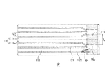
すなわち、上記アクティブ領域Laは、第1内部電極及び第2内部電極121、122と交互に積層配置される複数の第1誘電体層111aの間に、両側端部に段差吸収層112が配置された第2誘電体層111bが挿入された構造を有する。
That is, the active region L a is between the plurality of
上記の構造は、後述するように、焼成後、第1内部電極及び第2内部電極121、122となる導電性金属ペーストが塗布された第1セラミックグリーンシートを複数枚積層し、その上部に、両側端部にセラミック部材を形成して段差吸収層が形成された第2セラミックグリーンシートを積層することにより実現する。
In the above structure, as will be described later, after firing, a plurality of first ceramic green sheets coated with a conductive metal paste to be the first internal electrodes and the second
近年、積層されるセラミックグリーンシートの数が増加するに伴い、セラミックグリーンシートの積層工程と圧着工程を行う間に製品の信頼性に影響を及ぼすという問題点が発生している。 In recent years, as the number of ceramic green sheets to be laminated has increased, there has been a problem that the reliability of the product is affected during the laminating process and the crimping process of the ceramic green sheets.
すなわち、セラミックグリーンシートは、内部電極形成部と内部電極非形成部であるマージン部とからなり、セラミックグリーンシートが積層された後、所定の圧力が印加されて互いに圧着される場合、内部電極形成部と内部電極非形成部であるマージン部との段差が激しくなり、耐電圧特性が低下するという問題がある。 That is, the ceramic green sheet is composed of an internal electrode forming portion and a margin portion which is an internal electrode non-forming portion, and when the ceramic green sheet is laminated and then a predetermined pressure is applied to crimp each other, the internal electrode is formed. There is a problem that the step between the portion and the margin portion, which is the non-formed portion of the internal electrode, becomes large and the withstand voltage characteristic deteriorates.
上記のような段差の問題を改善するために、セラミック本体のマージン部に別のセラミック材料をネガティブ印刷(Negative Printing)工程により追加する技術があるが、この場合、セラミックグリーンシートで内部電極非形成部であるマージン部に別のセラミックスラリーを印刷する工程が非常に困難であるという問題がある。 In order to improve the problem of the step as described above, there is a technique of adding another ceramic material to the margin portion of the ceramic body by a negative printing (Negative Printing) process. In this case, the internal electrode is not formed by the ceramic green sheet. There is a problem that the process of printing another ceramic slurry on the margin portion, which is a portion, is very difficult.
また、マージン部に別のセラミック材料をネガティブ印刷(Negative Printing)工程により追加する方法は、精度が高くなく、積層後のセラミックグリーンシートの整列(Alignment)不良の問題によって段差の問題の改善効果が十分でない。 Further, the method of adding another ceramic material to the margin portion by the negative printing (Negative Printing) process does not have high accuracy, and the problem of poor alignment of the ceramic green sheet after lamination has an effect of improving the problem of step difference. not enough.
また、ネガティブ印刷(Negative Printing)工程を使用する場合、製造コストが増加し、工程自体の難易度が高くて不良率が高く、精密な製品の実現が困難であるという問題がある。 Further, when the negative printing process is used, there are problems that the manufacturing cost increases, the difficulty of the process itself is high, the defect rate is high, and it is difficult to realize a precise product.
しかし、本発明の一実施形態によると、上記アクティブ領域Laが第1内部電極及び第2内部電極121、122と交互に積層配置される複数の第1誘電体層111aの間に、両側端部に段差吸収層112が配置された第2誘電体層111bが挿入される構造を有することにより、段差の問題を改善して耐電圧特性が向上した高容量積層セラミック電子部品を実現することができる。
However, according to an embodiment of the present invention, during a plurality of
上記両側端部は、上記アクティブ領域Laのマージン部MW、MLに該当する領域であってもよい。 The side edge portions, the active region L a margin portion M W, or may be a region corresponding to M L.
すなわち、静電容量の形成に寄与するアクティブ領域Laは、第1内部電極及び第2内部電極121、122と交互に積層配置される複数の第1誘電体層111aと別に内部電極非形成部であるマージン部MW、MLに段差吸収層112が配置された少なくとも一つ以上の第2誘電体層111bが配置された構造を有する。
That is, the active region L a contribute to the formation of the electrostatic capacitance, separate internal electrode unformed portions and the plurality of
段差の問題を改善するために、セラミック本体のマージン部に別のセラミック材料をネガティブ印刷(Negative Printing)工程により追加する従来の構造は、第1内部電極及び第2内部電極と交互に積層配置される複数の誘電体層において、内部電極非形成部であるマージン部にセラミックスラリーを印刷する方法により実現するため、上記のような本発明の一実施形態に係る構造とは異なる。 In order to improve the problem of the step, another ceramic material is added to the margin portion of the ceramic body by a negative printing (Negative Printing) step, and the conventional structure is arranged alternately with the first internal electrode and the second internal electrode. Since it is realized by a method of printing a ceramic slurry on a margin portion which is an internal electrode non-forming portion in a plurality of dielectric layers, the structure is different from the structure according to the embodiment of the present invention as described above.
すなわち、従来の構造は、内部電極が印刷された誘電体層において内部電極非形成部であるマージン部にセラミックスラリーを印刷するため、内部電極と印刷されるセラミックスラリーは、同一水準で配置されるため、内部電極が印刷されていない別の誘電体層においてマージン部に該当する領域に段差吸収層を配置する本発明の構造とは異なる。 That is, in the conventional structure, since the ceramic slurry is printed on the margin portion which is the non-forming portion of the internal electrode in the dielectric layer on which the internal electrode is printed, the internal electrode and the printed ceramic slurry are arranged at the same level. Therefore, it is different from the structure of the present invention in which the step absorbing layer is arranged in the region corresponding to the margin portion in another dielectric layer on which the internal electrodes are not printed.
本発明の一実施形態によると、第1内部電極及び第2内部電極121、122と交互に積層配置される複数の第1誘電体層111aと別に内部電極非形成部であるマージン部MW、MLに段差吸収層112が配置された少なくとも一つ以上の第2誘電体層111bが交互に積層されるため、別のセラミック材料をネガティブ印刷(Negative Printing)する従来の方法とは異なって、工程が容易であり、積層後のセラミックグリーンシートの整列(Alignment)不良の問題がなく、段差改善の効果に優れる。
According to one embodiment of the present invention, a plurality of
本発明の一実施形態によると、上記段差吸収層112が配置された領域の側部に配置された誘電体層の厚さt1は、他の領域に配置された誘電体層の厚さt2より厚いことを特徴とする。
According to one embodiment of the present invention, the thickness t 1 of the dielectric layer arranged on the side of the region where the
ここで、誘電体層の厚さは、セラミック本体110のアクティブ領域Laにおいて、第1内部電極及び第2内部電極121、122が互いに対向する地点で測定されたものを意味する。
The thickness of the dielectric layer in the active region L a of the
すなわち、段差吸収層112が配置された領域の側部に配置された誘電体層の厚さt1は、上記アクティブ領域Laのマージン部MW、MLに配置された段差吸収層112と同一平面に配置された誘電体層の厚さであり、第1内部電極及び第2内部電極121、122が互いに対向する地点で測定されたものを意味する。
That is, the thickness t 1 of the
また、他の領域に配置された誘電体層の厚さt2は、アクティブ領域Laのマージン部MW、MLに配置された段差吸収層112と同一平面ではない領域に配置された誘電体層の厚さであり、第1内部電極及び第2内部電極121、122が互いに対向する地点で測定されたものを意味する。
The thickness t 2 of the dielectric layer disposed on the other region, is disposed in the active region L a margin portion M W, areas not arranged
上記段差吸収層112が配置された領域の側部に配置された誘電体層の厚さt1が他の領域に配置された誘電体層の厚さt2より厚い構造は、第1内部電極及び第2内部電極121、122と交互に積層配置される複数の第1誘電体層111aと別に内部電極非形成部であるマージン部MW、MLに段差吸収層112が配置された少なくとも一つ以上の第2誘電体層111bが交互に積層されることから実現されることができる。
A structure in which the thickness t 1 of the dielectric layer arranged on the side of the region where the
すなわち、アクティブ領域Laのマージン部MW、MLに配置された段差吸収層112と同一平面に配置された誘電体層は、他の位置に配置された誘電体層とは異なり、少なくとも2層以上の誘電体層が配置されるため、段差吸収層112が配置された誘電体層の厚さt1は、他の誘電体層の厚さt2より厚くなる。
In other words, the margin portion M W of the active region L a, dielectric layer disposed on the arranged
図2を参照すると、上記段差吸収層112は、上記セラミック本体の幅方向において、上記アクティブ領域Laのマージン部MWに該当する領域に配置されることができる。
Referring to FIG. 2, the
ただし、これに制限されるものではなく、上記段差吸収層112は、上記セラミック本体の幅方向と長さ方向において、上記アクティブ領域Laのマージン部MW、MLに該当する全領域に配置されてもよい。
However, this is not intended to be limiting, the
また、後述する図4のように、上記段差吸収層112は、上記セラミック本体の長さ方向において、上記アクティブ領域Laのマージン部MLに該当する領域にのみ配置されてもよい。
Further, as shown in FIG. 4 to be described later, the
図2及び図3を参照すると、上記第2誘電体層111bは、一面が第1内部電極121又は第2内部電極122と接し、他面が第1誘電体層111aと接することができる。
With reference to FIGS. 2 and 3, one surface of the second dielectric layer 111b can be in contact with the first
焼成後、第1内部電極及び第2内部電極121、122となる導電性金属ペーストが塗布された第1セラミックグリーンシートを複数枚積層し、その上部に、両側端部にセラミック部材を形成して段差吸収層が形成された第2セラミックグリーンシートを積層し、次に、その上部に複数枚の第1セラミックグリーンシートを積層する方法を繰り返すことによりアクティブ領域Laを形成することから、上記第2誘電体層111bは、一面が第1内部電極121又は第2内部電極122と接し、他面が第1誘電体層111aと接することができる。
After firing, a plurality of first ceramic green sheets coated with a conductive metal paste to be the first internal electrodes and the second
また、上記第2誘電体層111bの上下面のうち少なくとも一面には2層以上の第1誘電体層111aが積層されることができる。
Further, two or more first
すなわち、2層以上の第1誘電体層111aが積層され、その上部に上記第2誘電体層111bが積層された構造が繰り返されることにより、アクティブ領域Laが形成されることができる。
That is, two or more layers of the
上記第2誘電体層111bの上下面のうち少なくとも一面に配置される第1誘電体層111aの数は3層であってもよく、より多くの複数の第1誘電体層111aが配置されてもよい。
The number of the first
本発明の一実施形態によると、第1内部電極及び第2内部電極121、122が配置された2層以上の第1誘電体層111aを一つのユニットとしたときに、上記第2誘電体層111bは、2層以上の第1誘電体層111aで構成された一つのユニットと隣接したユニットとの間に配置されることができる。
According to one embodiment of the present invention, when two or more first
セラミック本体110の長さ及び/又は幅方向マージン部MW、MLに段差吸収層112が配置された第2誘電体層111bの層数は、特に制限されず、内部電極が積層されることによって発生する段差を相殺できる層数であってもよい。
Length and / or width direction margin portion M W of the ceramic body 110, the number of layers of the second dielectric layer 111b which
上記段差吸収層112の厚さは、特に制限されず、例えば、内部電極が積層されることによって発生する段差を相殺できる厚さであってもよい。
The thickness of the
上記段差吸収層112が配置された領域の側面に配置された誘電体層は、他の領域に配置された誘電体層より誘電体グレーンの個数がさらに多くてもよい。
The dielectric layer arranged on the side surface of the region where the
上記段差吸収層112が配置された誘電体層は、他の誘電体層とは異なり、少なくとも2層以上の誘電体層が配置されるため、誘電体グレーンの個数がより多くてもよい。
Unlike other dielectric layers, the dielectric layer in which the
本発明の一実施形態によると、上記段差吸収層112の厚さtbは、上記第1誘電体層111aの厚さtdより10倍〜20倍大きくてもよい。
According to one embodiment of the present invention, the thickness t b of the
上記段差吸収層112の厚さtbを上記第1誘電体層111aの厚さtdより10倍〜20倍大きく形成することにより、内部電極が積層されることによって発生する段差を相殺することができ、耐電圧特性を改善することができる。
By forming the thickness t b of the
例えば、第1誘電体層111aの厚さtdが0.4μmである場合、上記段差吸収層112の厚さtbは、4μm〜8μmであってもよい。
For example, when the thickness t d of the first dielectric layer 111 a is 0.4 μm, the thickness t b of the
本発明の一実施形態によると、上記第1内部電極及び第2内部電極121、122の積層方向において、第1内部電極及び第2内部電極121、122のうち上記段差吸収層112に隣接した二つの内部電極の端部は、隣接した段差吸収層112から離れる方向に曲がり得る。
According to one embodiment of the present invention, two of the first internal electrodes and the second
上記段差吸収層112に隣接した二つの内部電極の端部が隣接した段差吸収層112から離れる方向は、図2及び図3に図示されているように、内部電極或いは誘電体層の積層方向、すなわち、セラミック本体110の厚さ方向であり、段差吸収層112から離れる方向を意味することができる。
The direction in which the ends of the two internal electrodes adjacent to the
すなわち、第1誘電体層111aの厚さに比べて10倍〜20倍大きい厚さの段差吸収層112がセラミック本体110の長さ及び/又は幅方向マージン部MW、MLに配置されることにより、圧着過程で段差吸収層112の存在により段差吸収層112に隣接した二つの内部電極の端部は曲がり得る。
That is arranged
また、内部電極の端部は、段差吸収層112の存在により隣接した段差吸収層112から離れる方向に曲がり得る。
Further, the end portion of the internal electrode can be bent in a direction away from the adjacent
上記段差吸収層112に隣接した二つの内部電極121、122の端部の曲がり角度(θ)は、上記誘電体層111の積層面を基準として3度〜15度であってもよい。
The bending angle (θ) of the ends of the two
端部が誘電体層111の積層面を基準として3度〜15度曲がった内部電極は、上記段差吸収層112に隣接した二つの内部電極121、122の両方であってもよいが、これに制限されるものではなく、一部のみこれを満たしてもよい。
The internal electrodes whose ends are bent by 3 to 15 degrees with respect to the laminated surface of the
上記段差吸収層112に隣接した二つの内部電極121、122の端部が誘電体層111の積層面を基準として3度〜15度曲がることにより、耐電圧特性に優れ、且つ高容量積層セラミックキャパシターを実現することができる。
A high-capacity laminated ceramic capacitor with excellent withstand voltage characteristics by bending the ends of the two
すなわち、上記段差吸収層112に隣接した二つの内部電極121、122の端部が誘電体層111の積層面を基準として3度〜15度曲がるように制御することにより、目標設計容量を実現できるだけでなく、二つの内部電極の端部の間の間隔を一定に調節することができることから、ショートなどの不良を防ぐことができ、耐電圧特性を向上させることができる。
That is, the target design capacity can be realized by controlling the ends of the two
上記段差吸収層112に隣接した二つの内部電極121、122の端部が誘電体層111の積層面を基準に曲がる角度が3度未満である場合には、容量が減少して、高容量積層セラミックキャパシターを実現することができない。
When the angle at which the ends of the two
一方、上記段差吸収層112に隣接した二つの内部電極121、122の端部が誘電体層111の積層面を基準に曲がり角度が15度を超える場合には、耐電圧特性が低下する可能性がある。
On the other hand, if the ends of the two
本発明の一実施形態によると、上記段差吸収層112に隣接した二つの内部電極121、122の間の距離は、他の二つの内部電極の間の距離より大きくてもよい。
According to one embodiment of the present invention, the distance between the two
本発明の一実施形態では、段差吸収層112が配置された第2誘電体層111bが、2層以上の第1誘電体層111aで構成された一つのユニットと隣接したユニットとの間に配置されることから、段差吸収層112に隣接した二つの内部電極121、122の間には第1誘電体層111aと第2誘電体層111bが配置され、他の二つの内部電極の間には第1誘電体層111aのみが配置される。
In one embodiment of the present invention, the second dielectric layer 111b on which the
したがって、段差吸収層112に隣接した二つの内部電極121、122の間の距離は、他の二つの内部電極の間の距離より大きい。
Therefore, the distance between the two
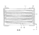
図4は本発明の一実施形態を説明するための図1のB−B'線に沿った断面図である。 FIG. 4 is a cross-sectional view taken along the line BB'of FIG. 1 for explaining one embodiment of the present invention.
図4を参照すると、上記段差吸収層112は、上記セラミック本体110の長さ方向において、上記アクティブ領域Laのマージン部MLに該当する領域に配置されることができる。
Referring to FIG. 4, the
上述のように、上記段差吸収層112は、上記セラミック本体110の長さ方向において、上記アクティブ領域Laのマージン部MLに該当する領域に配置されてもよく、幅方向マージン部MWに配置されてもよく、長さ方向と幅方向の両方に配置されてもよい。
As described above, the
セラミック本体110の長さ方向と幅方向マージン部MW、MLの両方に段差吸収層112が配置される場合、セラミック本体110の長さ方向マージン部MLに配置された段差吸収層112の厚さは、上記セラミック本体110の幅方向マージン部MWに配置された段差吸収層112の厚さより小さくてもよい。
The length and width directions margin part M W of the ceramic body 110, if the
例えば、セラミック本体110の長さ方向マージン部MLに配置された段差吸収層112の厚さは、上記セラミック本体110の幅方向マージン部MWに配置された段差吸収層112の厚さの1/2であってもよい。
For example, the thickness of the
セラミック本体110の長さ方向マージン部MLには、第1内部電極121と第2内部電極122が交互に配置されるため、内部電極非形成の幅方向マージン部MWに比べて電極密度がより高く、幅方向マージン部MWにおいて段差がより激しくなり得る。
The longitudinal margin portion M L of the
したがって、セラミック本体110の全体から見て段差の影響を最小化し、耐電圧特性を改善するために、電極密度がより高いセラミック本体110の長さ方向マージン部MLに配置された段差吸収層112の厚さは、上記セラミック本体110の幅方向マージン部MWに配置された段差吸収層112の厚さより小さいか、又は1/2に調節することができる。
Therefore, to minimize the influence of the steps when viewed from the whole of the
本発明の他の実施形態によると、誘電体層111と内部電極121、122が交互に積層されたセラミック本体110と、上記内部電極121、122と電気的に連結され、上記セラミック本体110の両端に形成される外部電極131、132と、を含み、上記セラミック本体110は、静電容量の形成に寄与するアクティブ領域La、及び上記アクティブ領域Laの上下面のうち少なくとも一面に提供される保護層Lcを含み、上記アクティブ領域Laの両側端部には少なくとも一つ以上のギャップ部112が配置され、上記ギャップ部112に隣接した二つの内部電極121、122の間の距離は、他の二つの内部電極の間の距離より大きい積層セラミック電子部品を提供する。
According to another embodiment of the present invention, the
上記ギャップ部112は、本発明の一実施形態により第2セラミックグリーンシートの両側端部にセラミック部材を形成して段差吸収層を形成し、導電性金属ペーストを用いて内部電極パターンを形成した複数の第1セラミックグリーンシートの間に挿入した後、積層及び圧着、焼成する場合に、段差吸収層によりセラミック本体のマージン部に形成される部分として定義されることができる。
A plurality of the
また、両側端部に段差吸収層が配置された第2セラミックグリーンシートが、2層以上の第1セラミックグリーンシートで構成された一つのユニットと隣接したユニットとの間に配置されるため、段差吸収層に隣接した二つの内部電極パターンの端部は曲がり得る。 Further, since the second ceramic green sheet having the step absorbing layers arranged on both side ends is arranged between one unit composed of two or more layers of the first ceramic green sheet and the adjacent unit, there is a step. The ends of the two internal electrode patterns adjacent to the absorption layer can be bent.
これにより、焼成後に、曲がった二つの内部電極の端部の辺りであるセラミック本体110のマージン部MW、MLにギャップ部112が配置されることができる。
Thus, after firing, the margin portion M W of the
また、両側端部に段差吸収層が配置された第2セラミックグリーンシートが、2層以上の第1セラミックグリーンシートで構成された一つのユニットと隣接したユニットとの間に配置されることから、段差吸収層に隣接した二つの内部電極パターンの間には第1セラミックグリーンシートと第2セラミックグリーンシートが配置され、他の二つの内部電極パターンの間には第1セラミックグリーンシートのみが配置される。 Further, since the second ceramic green sheet in which the step absorbing layers are arranged on both side ends is arranged between one unit composed of two or more layers of the first ceramic green sheet and the adjacent unit, The first ceramic green sheet and the second ceramic green sheet are arranged between the two internal electrode patterns adjacent to the step absorbing layer, and only the first ceramic green sheet is arranged between the other two internal electrode patterns. To.
したがって、焼成後、ギャップ部112に隣接した二つの内部電極121、122の間の距離は、他の二つの内部電極の間の距離より大きい。
Therefore, after firing, the distance between the two
また、焼成後、セラミック本体110のマージン部MW、MLには、曲がった二つの内部電極の端部の辺りにギャップ部112が配置されることから、ギャップ部112に隣接した二つの内部電極121、122の端部の間の距離は、他の二つの内部電極の端部の間の距離より大きい。
Moreover, after firing, the margin portion M W of the ceramic body 110, the M L, since it is disposed
上記ギャップ部112に隣接した二つの内部電極121、122の間の距離と、他の二つの内部電極の間の距離との差は、中央部より端部でより大きいことを特徴とする。
The difference between the distance between the two
上記の特徴は、焼成後、セラミック本体110のマージン部MW、MLには、曲がった二つの内部電極の端部の辺りにギャップ部112が配置されるためである。
The above features, after firing, the margin portion M W of the ceramic body 110, the M L, to around the end of the bent two internal electrodes is because the
その他の特徴は、上述の本発明の一実施形態に係る積層セラミック電子部品の特徴と同一であるため、ここでは省略する。 Other features are the same as the features of the laminated ceramic electronic component according to the embodiment of the present invention described above, and thus are omitted here.
本発明の他の実施形態は、誘電体層111と内部電極121、122が交互に積層されたセラミック本体110と、上記内部電極121、122と電気的に連結され、上記セラミック本体110の両端に形成される外部電極131、132と、を含み、上記セラミック本体110は、静電容量の形成に寄与するアクティブ領域La、及び上記アクティブ領域Laの上下面のうち少なくとも一面に提供される保護層Lcを含み、上記アクティブ領域Laの両側端部には、少なくとも一つ以上のギャップ部112が配置され、上記ギャップ部112に隣接した二つの内部電極121、122は、上記内部電極の積層方向において、上記ギャップ部112から離れる方向に曲がる積層セラミック電子部品を提供する。
In another embodiment of the present invention, the
本発明の他の実施形態に係る積層セラミック電子部品は、ギャップ部112に隣接した二つの内部電極121、122が上記内部電極の積層方向、すなわち、セラミック本体110の厚さ方向において、上記ギャップ部112から離れる方向に曲がることを特徴とする。
In the laminated ceramic electronic component according to another embodiment of the present invention, the two
上記の特徴以外は、上述の本発明の一実施形態に係る積層セラミック電子部品の特徴と同一であるため、ここでは省略する。 Other than the above-mentioned features, the features are the same as those of the laminated ceramic electronic component according to the above-described embodiment of the present invention, and thus are omitted here.
図5は本発明の他の実施形態を説明するための図1のA−A'線に沿った断面図である。 FIG. 5 is a cross-sectional view taken along the line AA'of FIG. 1 for explaining another embodiment of the present invention.
図5を参照すると、本発明の他の実施形態に係る積層セラミックキャパシターにおいて、第1内部電極及び第2内部電極121、122が製造過程で圧着されることにより、緩いカーブ状の形状を有することができることを示している。
Referring to FIG. 5, in the multilayer ceramic capacitor according to another embodiment of the present invention, the first internal electrode and the second
また、ギャップ部112に隣接した二つの内部電極121、122が上記内部電極の積層方向、すなわち、セラミック本体110の厚さ方向において、上記ギャップ部112から離れる方向に曲がる形状を有することができる。
Further, the two
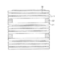
図6は本発明の一実施形態に係る積層セラミックキャパシターの積層構造を示す断面図である。 FIG. 6 is a cross-sectional view showing a laminated structure of a laminated ceramic capacitor according to an embodiment of the present invention.
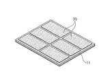
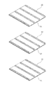
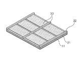
図6を参照すると、本発明の一実施形態に係る積層セラミックキャパシターは、導電性金属ペーストを用いて焼成した後、第1内部電極及び第2内部電極となる内部電極パターン30が形成された第1セラミックグリーンシート11を複数枚積層し、その上部に、両側端部にセラミック部材22を形成して段差吸収層が形成された第2セラミックグリーンシート21を積層し、その上部に複数枚の第1セラミックグリーンシート11を積層して形成された静電容量の形成に寄与するアクティブ領域Laを含む。
Referring to FIG. 6, in the multilayer ceramic capacitor according to the embodiment of the present invention, after firing using a conductive metal paste, an
上記のようにアクティブ領域Laが形成されることから、上記第2セラミックグリーンシート21は、一面が、焼成後、第1内部電極121又は第2内部電極122となる内部電極パターン30と接し、他面が、第1セラミックグリーンシート11と接することができる。
Since the active region L a is formed as described above, the second ceramic
上記第1セラミックグリーンシート11は、焼成後、第1誘電体層111aとなり、第2セラミックグリーンシート21は、焼成後、第2誘電体層111bとなる。
The first ceramic
両側端部にセラミック部材22を形成して段差吸収層が配置された第2セラミックグリーンシート21が、2層以上の第1セラミックグリーンシート11で構成された一つのユニットと隣接したユニットとの間に配置されることから、段差吸収層に隣接した二つの内部電極パターン30の間には第1セラミックグリーンシート11と第2セラミックグリーンシート21が配置され、他の二つの内部電極パターンの間には第1セラミックグリーンシート11のみが配置される。
The second ceramic
したがって、焼成後、段差吸収層112に隣接した二つの内部電極121、122の間の距離は、他の二つの内部電極の間の距離より大きい。
Therefore, after firing, the distance between the two
第2セラミックグリーンシート21の両側端部にセラミック部材22を形成する方法は、特に制限されるものではなく、例えば、印刷法により形成してもよく、パンチングにより形成してもよい。
The method of forming the
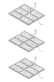
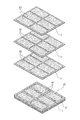
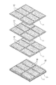
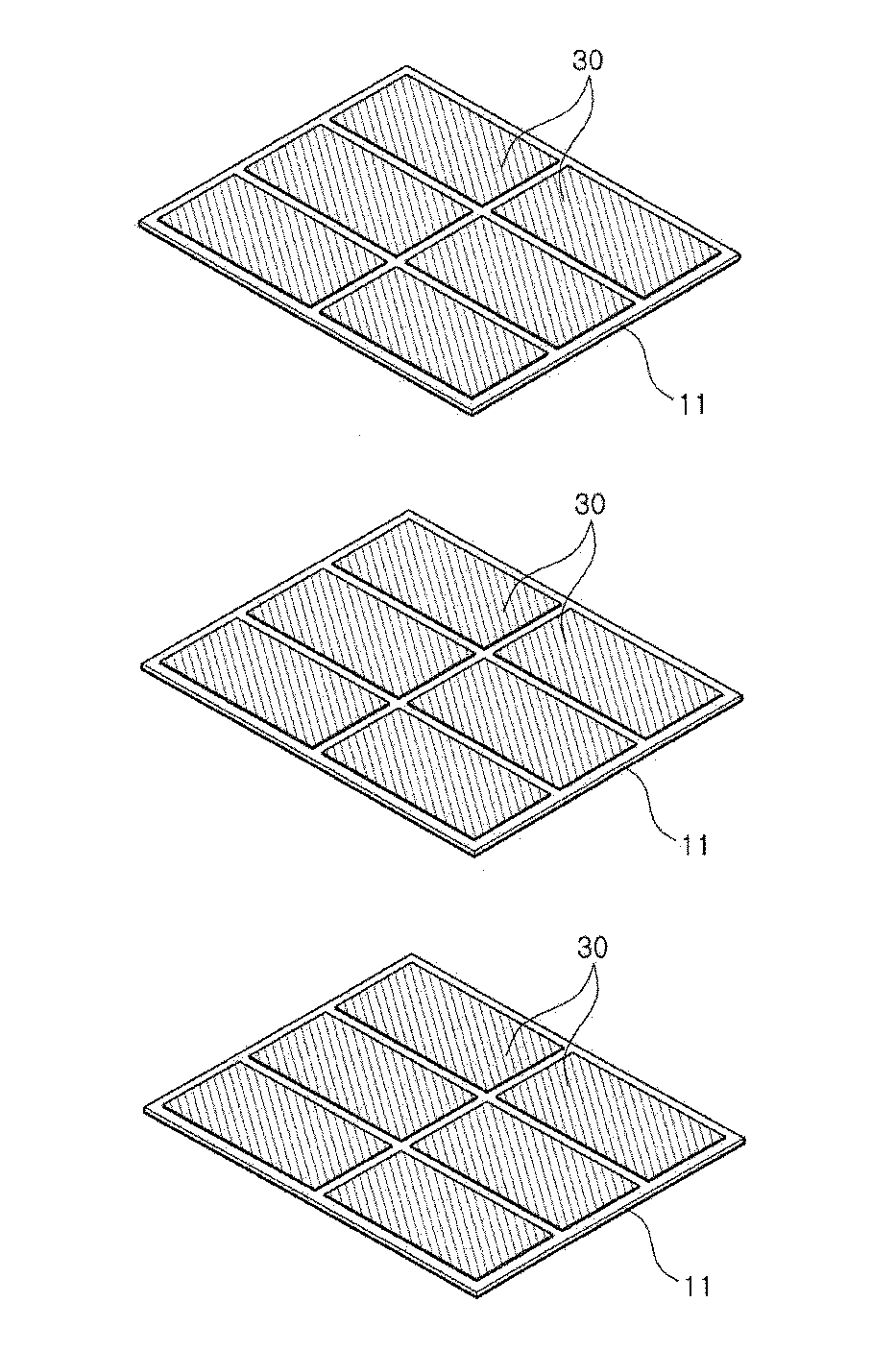
図7a〜図7eは本発明の他の実施形態に係る積層セラミックキャパシターの製造方法を示す工程図である。 7a to 7e are process diagrams showing a method for manufacturing a multilayer ceramic capacitor according to another embodiment of the present invention.
図7a〜図7eを参照すると、本発明の他の実施形態に係る積層セラミックキャパシターの製造方法は、第1及び第2セラミックグリーンシート11、21を製造する段階と、上記第1セラミックグリーンシート11上に導電性金属ペーストを用いて内部電極パターン30を形成する段階と、上記第2セラミックグリーンシート21の両側端部にセラミック部材22を形成して、段差吸収層を形成する段階と、上記第1及び第2セラミックグリーンシート11、21を積層して、誘電体層と第1内部電極及び第2内部電極を含むセラミック本体を形成する段階と、上記第1内部電極及び第2内部電極と電気的に連結される第1外部電極及び第2外部電極を形成する段階と、を含む。
With reference to FIGS. 7a to 7e, the method for manufacturing the multilayer ceramic capacitor according to another embodiment of the present invention includes the steps of manufacturing the first and second ceramic
上記セラミック本体は、静電容量の形成に寄与するアクティブ領域と、上記アクティブ領域の上下面のうち少なくとも一面に提供される保護層と、を含み、上記アクティブ領域は、少なくとも2層以上の第1セラミックグリーンシート11を積層し、その上部に第2セラミックグリーンシート21を積層する段階を繰り返すことにより形成される。
The ceramic body includes an active region that contributes to the formation of capacitance and a protective layer provided on at least one of the upper and lower surfaces of the active region, and the active region includes at least two or more first layers. It is formed by laminating the ceramic
本発明の他の実施形態に係る積層セラミックキャパシターの製造方法は、まず、第1及び第2セラミックグリーンシート11、21を製造する。
In the method for manufacturing a multilayer ceramic capacitor according to another embodiment of the present invention, first, the first and second ceramic
第1セラミックグリーンシート11は、一般的な積層セラミックキャパシターで使用されるセラミックグリーンシートと同様であり、上記第1セラミックグリーンシート11は、セラミック粉末、バインダー、溶剤を混合してスラリーを製造し、上記スラリーをドクターブレード法により数μmの厚さを有するシート(sheet)状に作製することができる。
The first ceramic
上記スラリーは、セラミック本体のアクティブ領域の一部の誘電体層と、及び保護層を構成する誘電体層を形成するセラミックグリーンシート用スラリーである。 The slurry is a slurry for a ceramic green sheet that forms a part of the dielectric layer in the active region of the ceramic body and the dielectric layer forming the protective layer.
第2セラミックグリーンシート21は、第1セラミックグリーンシート11と同様であるが、両側端部にセラミック部材22を形成して段差吸収層が形成される点で異なるため、異なるセラミックグリーンシートと名付けた。
The second ceramic
上記セラミック部材22は、上記第1セラミックグリーンシート11のように、セラミック粉末、バインダー、溶剤を混合したスラリー状であってもよいが、上記第1セラミックグリーンシート11を形成するスラリーとバインダー及び溶剤の含有量において異なる。
The
次に、上記第1セラミックグリーンシート11上に導電性金属ペーストを塗布して内部電極パターン30を形成する。
Next, the conductive metal paste is applied onto the first ceramic
上記内部電極パターン30は、スクリーン印刷法又はグラビア印刷法により形成されることができる。
The
図7aを参照すると、導電性金属ペーストを塗布して内部電極パターン30を形成した第1セラミックグリーンシート11を3枚示して一つのユニットと表現しており、このようなユニットが複数個作製されてもよい。また、一つのユニットをなす第1セラミックグリーンシート11の層数は、制限されず、例えば、2層以上であってもよい。
With reference to FIG. 7a, three first ceramic
次に、上記第2セラミックグリーンシート21の両側端部にセラミック部材22を形成して段差吸収層を形成する。
Next, the
図7bを参照すると、両側端部にセラミック部材22を形成して段差吸収層を形成した第2セラミックグリーンシート21を3枚示しているが、これに制限されるものではなく、複数個が作製されてもよい。
With reference to FIG. 7b, three second ceramic
第2セラミックグリーンシート21の両側端部にセラミック部材22を形成する方法は、特に制限されるものではなく、例えば、印刷法により形成してもよく、パンチングにより形成してもよい。
The method of forming the
図7cを参照すると、上記導電性金属ペーストを塗布して内部電極パターン30を形成した第1セラミックグリーンシート11を複数枚積層する。
With reference to FIG. 7c, a plurality of first ceramic
図7cでは、第1セラミックグリーンシート11を3枚積層しているが、これに制限されるものではない。
In FIG. 7c, three first ceramic
図7dを参照すると、一つのユニットである積層された第1セラミックグリーンシート11上に段差吸収層を形成した第2セラミックグリーンシート21を積層する。
With reference to FIG. 7d, the second ceramic
上記段差吸収層は、第2セラミックグリーンシート21において、第1セラミックグリーンシート11で導電性金属ペーストが塗布されていない部分、すなわち、焼成後、セラミック本体のマージン部となる領域と対応する領域に形成される。
The step absorbing layer is formed in the portion of the second ceramic
図7dでは、焼成後、セラミック本体の長さ方向及び幅方向マージン部に該当する全領域に段差吸収層が形成されていることを図示しているが、これに制限されるものではなく、長さ方向マージン部或いは幅方向マージン部にのみ形成することも可能である。 FIG. 7d shows that the step absorbing layer is formed in the entire region corresponding to the length direction and width direction margins of the ceramic body after firing, but the length is not limited to this. It is also possible to form only in the vertical margin portion or the width direction margin portion.
次に、上記第2セラミックグリーンシート21上に導電性金属ペーストを塗布して内部電極パターン30を形成した第1セラミックグリーンシート11を複数枚積層する。
Next, a plurality of first ceramic
図7eを参照すると、第2セラミックグリーンシート21上に導電性金属ペーストを塗布して内部電極パターン30を形成した第1セラミックグリーンシート11を3枚積層することが図示されているが、これに制限されるものではない。
With reference to FIG. 7e, it is shown that three first ceramic
また、第2セラミックグリーンシート21上に積層される第1セラミックグリーンシート11は、1枚ずつ積層してもよく、積層された第1セラミックグリーンシート11ユニットを積層してもよい。
Further, the first ceramic
このように積層される場合、複数個の第1セラミックグリーンシート11で構成された一つのユニットと隣接した他のユニットとの間に段差吸収層を形成した第2セラミックグリーンシート21が挿入された形態で積層され、このような方法を繰り返して行うことにより、積層数を増加させることができる。
When laminated in this way, the second ceramic
次に、上記複数のセラミックグリーンシートを積層し、積層方向から加圧して、積層されたセラミックグリーンシートと内部電極ペーストを互いに圧着させる。 Next, the plurality of ceramic green sheets are laminated and pressed from the stacking direction to press the laminated ceramic green sheets and the internal electrode paste against each other.
このようにして、セラミックグリーンシートと内部電極ペーストが交互に積層されたセラミック積層体を製造する。 In this way, a ceramic laminate in which ceramic green sheets and internal electrode pastes are alternately laminated is produced.
この際、両側端部にセラミック部材22を形成した第2セラミックグリーンシート21は、上記セラミック積層体のマージン部に段差吸収層を形成する。
At this time, the second ceramic
上記段差吸収層により、上記セラミック積層体において内部電極による段差の発生率が減少し、これにより耐電圧が改善する。 The step absorbing layer reduces the occurrence rate of steps caused by the internal electrodes in the ceramic laminate, thereby improving the withstand voltage.
次に、セラミック積層体を一つのキャパシターに対応する領域ごとに切断し、チップ化する。 Next, the ceramic laminate is cut into chips in each region corresponding to one capacitor.
この際、第1内部電極及び第2内部電極パターンの一端が側面に交互に露出するように切断する。 At this time, the first internal electrode and the second internal electrode pattern are cut so that one ends are alternately exposed on the side surfaces.
次に、チップ化した積層体を、例えば、1200℃程度に焼成して、誘電体層と第1内部電極及び第2内部電極を含むセラミック本体を製造する。 Next, the chipped laminate is fired at, for example, about 1200 ° C. to produce a ceramic body including a dielectric layer, a first internal electrode, and a second internal electrode.
次に、セラミック本体の両端を覆い、セラミック本体の側面に露出した第1内部電極及び第2内部電極と電気的に連結されるように第1外部電極及び第2外部電極を形成する。 Next, both ends of the ceramic body are covered, and the first external electrode and the second external electrode are formed so as to be electrically connected to the first internal electrode and the second internal electrode exposed on the side surface of the ceramic body.
次に、外部電極の表面にニッケル、スズなどのめっき処理を施すことができる。 Next, the surface of the external electrode can be plated with nickel, tin, or the like.
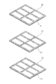
図8a〜図8eは本発明の他の実施形態に係る積層セラミックキャパシターの製造方法を示す工程図である。 8a to 8e are process diagrams showing a method for manufacturing a multilayer ceramic capacitor according to another embodiment of the present invention.
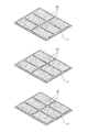
図8a〜図8eを参照すると、第2セラミックグリーンシート21にセラミック部材22を形成する工程において、セラミック本体の幅方向に、アクティブ領域のマージン部に該当する領域にセラミック部材22を形成した以外は、図7a〜図7eに係る積層セラミックキャパシターの製造方法と同一である。
With reference to FIGS. 8a to 8e, in the step of forming the
図9a〜図9eは本発明の他の実施形態に係る積層セラミックキャパシターの製造方法を示す工程図である。 9a to 9e are process diagrams showing a method for manufacturing a multilayer ceramic capacitor according to another embodiment of the present invention.
図9a〜図9eを参照すると、第2セラミックグリーンシート21にセラミック部材22を形成する工程において、セラミック本体の長さ方向に、アクティブ領域のマージン部に該当する領域にセラミック部材22を形成した以外は、図7a〜図7eによる積層セラミックキャパシターの製造方法と同一である。
With reference to FIGS. 9a to 9e, in the step of forming the
下記の表1は第1内部電極及び第2内部電極の積層方向において、上記第1内部電極及び第2内部電極の端部の曲がり角度による積層セラミックキャパシターの静電容量と耐電圧特性を比較した表である。 Table 1 below compares the capacitance and withstand voltage characteristics of the laminated ceramic capacitor depending on the bending angle of the ends of the first internal electrode and the second internal electrode in the stacking direction of the first internal electrode and the second internal electrode. It is a table.
上記表1において、静電容量は、目標静電容量を10%以上超える場合には非常に良好(◎)、0.0%〜10%である場合には良好(○)、目標静電容量未満である場合には不良(×)と判定した。 In Table 1 above, the capacitance is very good (⊚) when it exceeds the target capacitance by 10% or more, good (◯) when it exceeds 0.0% to 10%, and the target capacitance. If it is less than, it is judged as defective (x).
耐電圧特性の場合、目標耐電圧を10%以上超える場合には非常に良好(◎)、0.0%〜10%である場合には良好(○)、目標静電容量未満である場合には不良(×)と判定した。 In the case of withstand voltage characteristics, it is very good when the target withstand voltage exceeds 10% (◎), good when it is 0.0% to 10% (○), and when it is less than the target capacitance. Was judged to be defective (x).
上記表1を参照すると、第1内部電極及び第2内部電極の端部の曲がり角度(θ)が3度〜15度の範囲内にある場合に、高容量で、耐電圧特性に優れ、信頼性が改善することが分かる。 With reference to Table 1 above, when the bending angle (θ) of the ends of the first internal electrode and the second internal electrode is within the range of 3 degrees to 15 degrees, the capacity is high, the withstand voltage characteristics are excellent, and reliability is high. It can be seen that the sex improves.
一方、試料1〜3の場合には、第1内部電極及び第2内部電極の端部の曲がり角度(θ)が3度未満であり、静電容量が減少するという問題があり、試料13及び14の場合には、第1内部電極及び第2内部電極の端部の曲がり角度(θ)が15度を超え、耐電圧特性が低下するという問題がある。 On the other hand, in the case of Samples 1 to 3, there is a problem that the bending angle (θ) of the ends of the first internal electrode and the second internal electrode is less than 3 degrees and the capacitance is reduced. In the case of 14, there is a problem that the bending angle (θ) of the ends of the first internal electrode and the second internal electrode exceeds 15 degrees and the withstand voltage characteristic is deteriorated.
以上、本発明の実施形態について詳細に説明したが、本発明の範囲はこれに限定されず、特許請求の範囲に記載された本発明の技術的思想から外れない範囲内で多様な修正及び変形が可能であるということは、当技術分野の通常の知識を有する者には明らかである。 Although the embodiments of the present invention have been described in detail above, the scope of the present invention is not limited to this, and various modifications and modifications are made without departing from the technical idea of the present invention described in the claims. It is clear to those with ordinary knowledge in the art that this is possible.
100 積層セラミックキャパシター
110 セラミック本体
111 誘電体層
112 段差吸収層(ギャップ部)
121、122 第1内部電極及び第2内部電極
131、132 第1外部電極及び第2外部電極
100
121, 122 First internal electrode and second
Claims (39)
前記第1内部電極及び第2内部電極と電気的に連結され、前記セラミック本体の両端に形成される第1外部電極及び第2外部電極と、を含み、
前記アクティブ領域内には、前記セラミック本体の長さ方向の両側端部及び幅方向の両側端部のうち少なくとも一つ以上に段差吸収層が配置され、前記段差吸収層が配置された領域の側部に配置された誘電体層の厚さは、他の領域に配置された誘電体層の厚さより厚く、
前記第1内部電極及び第2内部電極の積層方向において、前記第1内部電極及び前記第2内部電極のうち、前記段差吸収層の前記積層方向の一方側と他方側とにそれぞれ隣接した二つの内部電極の端部は、隣接した前記段差吸収層から離れる方向に曲がり、
前記段差吸収層の厚さは、前記段差吸収層が配置された誘電体層以外の他の誘電体層の厚さより10倍〜20倍大きい、
積層セラミック電子部品。 Includes an active region in which a dielectric layer, first internal electrodes, and second internal electrodes are alternately laminated and contributes to the formation of capacitance, and a protective layer provided on at least one of the upper and lower surfaces of the active region. With the ceramic body
Includes a first external electrode and a second external electrode that are electrically connected to the first internal electrode and the second internal electrode and are formed at both ends of the ceramic body.
In the active region, a step absorbing layer is arranged at least one of both side ends in the length direction and both side ends in the width direction of the ceramic body, and the side of the region where the step absorbing layer is arranged. The thickness of the dielectric layer arranged in the portion is thicker than the thickness of the dielectric layer arranged in the other region.
In the stacking direction of the first internal electrode and the second internal electrode, two of the first internal electrode and the second internal electrode are adjacent to one side and the other side of the step absorbing layer in the stacking direction, respectively. ends of the internal electrodes, tracks away from adjacent the step absorption layer is Ri,
The thickness of the step absorbing layer is 10 to 20 times larger than the thickness of the dielectric layer other than the dielectric layer on which the step absorbing layer is arranged.
Multilayer ceramic electronic components.
前記内部電極と電気的に連結され、前記セラミック本体の両端に形成される外部電極と、を含み、
前記アクティブ領域の両側端部には、少なくとも一つ以上のギャップ部が配置され、前記ギャップ部に隣接した二つの内部電極の間の距離は、他の二つの内部電極の間の距離より大きく、
前記内部電極の積層方向において、前記ギャップ部の前記積層方向の一方側と他方側とにそれぞれ隣接した二つの内部電極の端部は、隣接した前記ギャップ部から離れる方向に曲がり、
前記ギャップ部の厚さは、前記ギャップ部が配置された誘電体層以外の他の誘電体層の厚さより10倍〜20倍大きい、
積層セラミック電子部品。 An active region in which dielectric layers and internal electrodes are alternately laminated and contributes to the formation of capacitance, a ceramic body including a protective layer provided on at least one of the upper and lower surfaces of the active region, and a ceramic body.
Includes external electrodes that are electrically connected to the internal electrodes and are formed at both ends of the ceramic body.
At least one or more gap portions are arranged at both end portions of the active region, and the distance between the two internal electrodes adjacent to the gap portion is larger than the distance between the other two internal electrodes.
In the stacking direction of the internal electrodes, the ends of the two internal electrodes adjacent each of the to the one side and the other side in the stacking direction of the gap portion, Ri songs in a direction away from adjacent the gap portion,
The thickness of the gap portion is 10 to 20 times larger than the thickness of the dielectric layer other than the dielectric layer in which the gap portion is arranged.
Multilayer ceramic electronic components.
前記内部電極と電気的に連結され、前記セラミック本体の両端に形成される外部電極と、を含み、
前記アクティブ領域の両側端部には、少なくとも一つ以上のギャップ部が配置され、前記内部電極の積層方向において、前記ギャップ部の前記積層方向の一方側と他方側とにそれぞれ隣接した二つの内部電極は、前記ギャップ部から離れる方向に曲がり、
前記ギャップ部の厚さは、前記ギャップ部が配置された誘電体層以外の他の誘電体層の厚さより10倍〜20倍大きい、
積層セラミック電子部品。 A ceramic body including an active region in which dielectric layers and internal electrodes are alternately laminated and contributes to the formation of capacitance, and a protective layer provided on at least one of the upper and lower surfaces of the active region.
Includes external electrodes that are electrically connected to the internal electrodes and are formed at both ends of the ceramic body.
At least one or more gap portions are arranged at both end portions of the active region, and in the stacking direction of the internal electrodes, two internal portions adjacent to one side and the other side of the gap portion in the stacking direction, respectively. electrodes, song Ri in a direction away from the gap portion,
The thickness of the gap portion is 10 to 20 times larger than the thickness of the dielectric layer other than the dielectric layer in which the gap portion is arranged.
Multilayer ceramic electronic components.
前記第1セラミックグリーンシート上に導電性金属ペーストを用いて内部電極パターンを形成する段階と、
前記第2セラミックグリーンシートの長さ方向の両側端部及び幅方向の両側端部のうち少なくとも一つ以上にセラミック部材を形成して、段差吸収層を形成する段階と、
前記第1及び第2セラミックグリーンシートを積層して、誘電体層と第1内部電極及び第2内部電極を含むセラミック本体を形成する段階と、
前記第1内部電極及び第2内部電極と電気的に連結される第1外部電極及び第2外部電極を形成する段階と、を含み、
前記セラミック本体は、静電容量の形成に寄与するアクティブ領域、及び前記アクティブ領域の上下面のうち少なくとも一面に提供される保護層を含み、前記アクティブ領域は、少なくとも2層以上の第1セラミックグリーンシートを積層し、その上部に第2セラミックグリーンシートを積層する段階を繰り返すことにより形成され、
前記第1内部電極及び第2内部電極の積層方向において、第1内部電極及び第2内部電極のうち、前記段差吸収層の前記積層方向の一方側と他方側とにそれぞれ隣接した二つの内部電極の端部は、隣接した前記段差吸収層から離れる方向に曲がり、
前記段差吸収層の厚さは、前記第1セラミックグリーンシートの厚さより10倍〜20倍大きい、
積層セラミック電子部品の製造方法。 The stage of manufacturing the first and second ceramic green sheets,
The stage of forming an internal electrode pattern on the first ceramic green sheet using a conductive metal paste, and
A step of forming a step absorbing layer by forming a ceramic member at least one of both side ends in the length direction and both side ends in the width direction of the second ceramic green sheet.
A step of laminating the first and second ceramic green sheets to form a ceramic body including a dielectric layer, a first internal electrode, and a second internal electrode.
Including a step of forming a first external electrode and a second external electrode that are electrically connected to the first internal electrode and the second internal electrode.
The ceramic body includes an active region that contributes to the formation of capacitance and a protective layer provided on at least one of the upper and lower surfaces of the active region, and the active region includes at least two or more first ceramic greens. It is formed by repeating the steps of laminating sheets and laminating a second ceramic green sheet on top of them.
In the stacking direction of the first internal electrode and the second internal electrode, of the first internal electrode and the second internal electrode, two internal electrodes adjacent to one side and the other side of the step absorbing layer in the stacking direction, respectively. end of the song in a direction away from adjacent the step absorption layer is Ri,
The thickness of the step absorbing layer is 10 to 20 times larger than the thickness of the first ceramic green sheet.
Manufacturing method for monolithic ceramic electronic components.
前記第1内部電極及び第2内部電極と電気的に連結され、前記セラミック本体の両端に形成される第1外部電極及び第2外部電極と、を含み、
前記段差吸収層は、前記セラミック本体の一端面において前記第1内部電極の上部に配置され、他端面において前記第2内部電極の下部に配置され、
前記第1内部電極及び第2内部電極の積層方向において、第1内部電極及び第2内部電極のうち、記段差吸収層の前記積層方向の一方側と他方側とにそれぞれ隣接した二つの内部電極の端部は、隣接した前記段差吸収層から離れる方向に曲がり、
前記段差吸収層の厚さは、第1内部電極及び第2内部電極の間に配置された誘電体層のうち一つの厚さに対して10倍以上である、
積層セラミック電子部品。 A ceramic body including a first internal electrode and a second internal electrode alternately arranged via a dielectric layer, and a step absorbing layer arranged in a margin portion extending on both sides in the width direction.
Includes a first external electrode and a second external electrode that are electrically connected to the first internal electrode and the second internal electrode and are formed at both ends of the ceramic body.
The step absorbing layer is arranged above the first internal electrode on one end surface of the ceramic body and below the second internal electrode on the other end surface.
In the stacking direction of the first internal electrode and the second internal electrode, of the first internal electrode and the second internal electrode, two internal electrodes adjacent to one side and the other side of the step absorption layer in the stacking direction, respectively. end of the song in a direction away from adjacent the step absorption layer is Ri,
The thickness of the step absorbing layer is 10 times or more the thickness of one of the dielectric layers arranged between the first internal electrode and the second internal electrode.
Multilayer ceramic electronic components.
前記第1セラミックグリーンシートのマージン部に対応する第2セラミックグリーンシートの領域上にセラミック部材を形成する段階と、
複数の第1セラミックグリーンシート上に前記第2セラミックグリーンシートのうち一つ以上を積層する段階と、
積層方向において、前記セラミック部材の前記積層方向の一方側と他方側とにそれぞれに隣接した二つの内部電極の端部は、隣接した前記セラミック部材から離れる方向に曲がるように前記積層された第1及び第2セラミックグリーンシートを焼成する段階と、を含み、
前記セラミック部材が前記第1セラミックグリーンシートの厚さに対して10倍以上の厚さを有するように前記積層された第1及び第2セラミックグリーンシートを焼成する段階をさらに含む、
積層セラミック電子部品の製造方法。 The stage of forming the internal electrode pattern on the first ceramic green sheet separated by one or more surfaces by the margin part, and
The stage of forming a ceramic member on the region of the second ceramic green sheet corresponding to the margin portion of the first ceramic green sheet, and
The stage of laminating one or more of the second ceramic green sheets on a plurality of first ceramic green sheets, and
In the stacking direction, the ends of the two internal electrodes adjacent to one side and the other side of the ceramic member in the stacking direction are the first stacked so as to bend in a direction away from the adjacent ceramic member. and a step of firing the second ceramic green sheet, only including,
Further including a step of firing the laminated first and second ceramic green sheets so that the ceramic member has a thickness of 10 times or more the thickness of the first ceramic green sheet.
Manufacturing method for monolithic ceramic electronic components.
内部電極パターンと電気的に連結されるように前記積層された第1及び第2セラミックグリーンシートの端部に外部電極を形成する段階と、をさらに含む、請求項35に記載の積層セラミック電子部品の製造方法。 A step of forming a protective layer on the upper surface or the lower surface of the laminated first and second ceramic green sheets, and
The laminated ceramic electronic component according to claim 35 , further comprising a step of forming an external electrode at the end of the laminated first and second ceramic green sheets so as to be electrically connected to the internal electrode pattern. Manufacturing method.
Applications Claiming Priority (2)
| Application Number | Priority Date | Filing Date | Title |
|---|---|---|---|
| KR1020150167490A KR101762032B1 (en) | 2015-11-27 | 2015-11-27 | Multi-layer ceramic electronic part and method for manufacturing the same |
| KR10-2015-0167490 | 2015-11-27 |
Publications (2)
| Publication Number | Publication Date |
|---|---|
| JP2017098524A JP2017098524A (en) | 2017-06-01 |
| JP6834091B2 true JP6834091B2 (en) | 2021-02-24 |
Family
ID=58777752
Family Applications (1)
| Application Number | Title | Priority Date | Filing Date |
|---|---|---|---|
| JP2016143778A Active JP6834091B2 (en) | 2015-11-27 | 2016-07-21 | Multilayer ceramic electronic components and their manufacturing methods |
Country Status (4)
| Country | Link |
|---|---|
| US (2) | US10304632B2 (en) |
| JP (1) | JP6834091B2 (en) |
| KR (1) | KR101762032B1 (en) |
| CN (2) | CN106816312B (en) |
Families Citing this family (19)
| Publication number | Priority date | Publication date | Assignee | Title |
|---|---|---|---|---|
| KR102437801B1 (en) | 2016-02-22 | 2022-08-30 | 삼성전기주식회사 | Multi-layer ceramic electronic part and method for manufacturing the same |
| JP6696464B2 (en) * | 2017-03-15 | 2020-05-20 | 株式会社村田製作所 | Method for manufacturing monolithic ceramic electronic component |
| KR101952871B1 (en) | 2017-04-13 | 2019-02-28 | 삼성전기주식회사 | Multi layer ceramic capacitor and board having the same |
| JP6841716B2 (en) * | 2017-04-27 | 2021-03-10 | 太陽誘電株式会社 | Multilayer ceramic capacitors and their manufacturing methods |
| KR102527705B1 (en) * | 2018-10-10 | 2023-05-02 | 삼성전기주식회사 | Multilayer ceramic electronic component |
| KR102691306B1 (en) * | 2018-11-13 | 2024-08-05 | 삼성전기주식회사 | Multilayer ceramic electronic component |
| JP7604741B2 (en) * | 2019-02-20 | 2024-12-24 | サムソン エレクトロ-メカニックス カンパニーリミテッド. | Stacked capacitor and method of manufacturing same |
| JP7506514B2 (en) * | 2019-07-16 | 2024-06-26 | 太陽誘電株式会社 | Manufacturing method for multilayer ceramic electronic components |
| KR102737552B1 (en) * | 2019-07-18 | 2024-12-03 | 삼성전기주식회사 | Multilayered capacitor and board having the same mounted thereon |
| KR102797230B1 (en) * | 2019-07-24 | 2025-04-18 | 삼성전기주식회사 | Multi-layered ceramic capacitor |
| JP2021040100A (en) * | 2019-09-05 | 2021-03-11 | 株式会社村田製作所 | Monolithic ceramic capacitor |
| KR102282846B1 (en) * | 2019-09-17 | 2021-07-28 | 서순기 | Electrode laminated structure for electrolyzed sterilizing water producing apparatus |
| JP7192741B2 (en) * | 2019-10-30 | 2022-12-20 | 株式会社村田製作所 | LAMINATED CERAMIC ELECTRONIC COMPONENT AND METHOD FOR MANUFACTURING LAMINATED CERAMIC ELECTRONIC COMPONENT |
| CN111834126B (en) * | 2020-06-12 | 2022-05-31 | 深圳三环电子有限公司 | Multilayer ceramic capacitor and preparation method thereof |
| JP2022075191A (en) * | 2020-11-06 | 2022-05-18 | 株式会社村田製作所 | Multilayer ceramic capacitor and manufacturing method for multilayer ceramic capacitor |
| KR102900298B1 (en) * | 2021-10-15 | 2025-12-12 | 삼성전기주식회사 | Capacitor component |
| KR20240091618A (en) | 2022-12-14 | 2024-06-21 | 삼성전기주식회사 | Multilayer electronic component |
| CN116494349A (en) * | 2023-05-23 | 2023-07-28 | 北京元六鸿远电子科技股份有限公司 | Ceramic green body with stacked ceramic diaphragms |
| KR20250075140A (en) * | 2023-11-21 | 2025-05-28 | 삼성전기주식회사 | Multilayer electronic component |
Family Cites Families (29)
| Publication number | Priority date | Publication date | Assignee | Title |
|---|---|---|---|---|
| JPH02100306A (en) * | 1988-10-07 | 1990-04-12 | Murata Mfg Co Ltd | Manufacture of laminated electronic component |
| JP3025379B2 (en) * | 1992-08-28 | 2000-03-27 | 京セラ株式会社 | Manufacturing method of multilayer capacitor |
| JP3544569B2 (en) | 1994-11-24 | 2004-07-21 | 京セラ株式会社 | Multilayer ceramic capacitors |
| JP3758442B2 (en) * | 1999-02-23 | 2006-03-22 | 株式会社村田製作所 | Manufacturing method of multilayer ceramic capacitor |
| JP3535998B2 (en) * | 1999-03-29 | 2004-06-07 | 太陽誘電株式会社 | Multilayer ceramic electronic components |
| JP3767362B2 (en) * | 1999-12-13 | 2006-04-19 | 株式会社村田製作所 | Manufacturing method of multilayer ceramic electronic component |
| JP2004269325A (en) | 2003-03-10 | 2004-09-30 | Murata Mfg Co Ltd | Method of manufacturing ceramic paste, and method of manufacturing laminated ceramic electronic component using ceramic paste |
| JP2005072452A (en) | 2003-08-27 | 2005-03-17 | Kyocera Corp | Multilayer electronic component and manufacturing method thereof |
| JP2006278566A (en) | 2005-03-28 | 2006-10-12 | Tdk Corp | Multilayer electronic component and its manufacturing method |
| JP2006332285A (en) | 2005-05-25 | 2006-12-07 | Tdk Corp | Stacked ceramic capacitor and method of manufacturing same |
| JP4418969B2 (en) * | 2005-06-03 | 2010-02-24 | 株式会社村田製作所 | Multilayer ceramic capacitor |
| JP4807169B2 (en) | 2006-07-07 | 2011-11-02 | 株式会社村田製作所 | Multilayer ceramic capacitor and manufacturing method thereof |
| JP4760857B2 (en) * | 2008-05-29 | 2011-08-31 | Tdk株式会社 | Manufacturing method of multilayer electronic component |
| JP2010040628A (en) * | 2008-08-01 | 2010-02-18 | Taiyo Yuden Co Ltd | Laminated type ceramic electronic component manufacturing method |
| KR101079382B1 (en) * | 2009-12-22 | 2011-11-02 | 삼성전기주식회사 | multilayer ceramic capacitor and fabricating method of the same |
| KR101288154B1 (en) * | 2010-12-06 | 2013-07-18 | 삼성전기주식회사 | A MUlLTI LAYERED CERAMIC DEVICE AND FABRICATING METHOD THEREOF |
| KR101843182B1 (en) * | 2011-05-31 | 2018-03-28 | 삼성전기주식회사 | Multilayer ceramic electronic component |
| KR101952845B1 (en) | 2011-12-22 | 2019-02-28 | 삼성전기주식회사 | Multi-layer ceramic electronic part and method for manufacturing the same |
| JP5960816B2 (en) * | 2012-06-21 | 2016-08-02 | 京セラ株式会社 | Multilayer ceramic capacitor |
| KR101922866B1 (en) * | 2012-07-19 | 2019-02-27 | 삼성전기 주식회사 | Multi-Layered Ceramic Electronic Component and Manufacturing Method of the Same |
| JP5874682B2 (en) * | 2012-08-09 | 2016-03-02 | 株式会社村田製作所 | Capacitor component and capacitor component mounting structure |
| KR101376843B1 (en) * | 2012-11-29 | 2014-03-20 | 삼성전기주식회사 | Multi-layered ceramic capacitor, mounting structure of circuit having thereon multi-layered ceramic capacitor and packing unit for multi-layered ceramic capacitor |
| JP2014127581A (en) * | 2012-12-26 | 2014-07-07 | Taiyo Yuden Co Ltd | Multilayer ceramic electronic component |
| KR101462754B1 (en) * | 2013-01-24 | 2014-11-17 | 삼성전기주식회사 | Multi-layered ceramic electronic parts and fabricating method thereof |
| KR101514512B1 (en) * | 2013-04-08 | 2015-04-22 | 삼성전기주식회사 | A multilayer ceramic capacitor and a method for manufactuaring the same |
| KR101548797B1 (en) * | 2013-04-08 | 2015-08-31 | 삼성전기주식회사 | A multilayer ceramic capacitor and a method for manufactuaring the same |
| CN104576057B (en) * | 2014-12-23 | 2017-07-04 | 广东风华高新科技股份有限公司 | Multilayer ceramic capacitor |
| JP6218725B2 (en) * | 2014-12-26 | 2017-10-25 | 太陽誘電株式会社 | Multilayer ceramic capacitor |
| KR102437801B1 (en) * | 2016-02-22 | 2022-08-30 | 삼성전기주식회사 | Multi-layer ceramic electronic part and method for manufacturing the same |
-
2015
- 2015-11-27 KR KR1020150167490A patent/KR101762032B1/en not_active Expired - Fee Related
-
2016
- 2016-07-21 JP JP2016143778A patent/JP6834091B2/en active Active
- 2016-07-22 US US15/217,233 patent/US10304632B2/en active Active
- 2016-08-12 CN CN201610663897.5A patent/CN106816312B/en not_active Expired - Fee Related
- 2016-08-12 CN CN201910454995.1A patent/CN110246690B/en not_active Expired - Fee Related
-
2019
- 2019-04-03 US US16/374,000 patent/US10943736B2/en active Active
Also Published As
| Publication number | Publication date |
|---|---|
| CN110246690B (en) | 2021-09-21 |
| CN106816312B (en) | 2019-07-02 |
| US20190228912A1 (en) | 2019-07-25 |
| CN106816312A (en) | 2017-06-09 |
| KR20170062087A (en) | 2017-06-07 |
| JP2017098524A (en) | 2017-06-01 |
| US20170154733A1 (en) | 2017-06-01 |
| CN110246690A (en) | 2019-09-17 |
| US10943736B2 (en) | 2021-03-09 |
| KR101762032B1 (en) | 2017-07-26 |
| US10304632B2 (en) | 2019-05-28 |
Similar Documents
| Publication | Publication Date | Title |
|---|---|---|
| JP6834091B2 (en) | Multilayer ceramic electronic components and their manufacturing methods | |
| KR102527706B1 (en) | Multi-layer ceramic electronic part and method for manufacturing the same | |
| JP7315138B2 (en) | Multilayer ceramic capacitor | |
| JP5551296B1 (en) | Multilayer ceramic capacitor and manufacturing method thereof | |
| JP5332475B2 (en) | Multilayer ceramic electronic component and manufacturing method thereof | |
| JP5420619B2 (en) | Multilayer ceramic capacitor and manufacturing method thereof | |
| JP7586458B2 (en) | Multilayer ceramic capacitor and its manufacturing method | |
| JP5653886B2 (en) | Multilayer ceramic capacitor and manufacturing method thereof | |
| JP2021044533A (en) | Multilayer ceramic capacitors and their manufacturing methods | |
| JP2015146454A (en) | Multilayer ceramic capacitor and method of manufacturing the same | |
| JP2012253337A (en) | Multilayer ceramic electronic component | |
| CN113035569A (en) | Multilayer ceramic capacitor and method for manufacturing the same | |
| KR102097328B1 (en) | Multi-layer ceramic electronic part and method for manufacturing the same | |
| JP6261855B2 (en) | Multilayer ceramic electronic component and manufacturing method thereof | |
| JP2020035991A (en) | Multilayer ceramic capacitor and manufacturing method thereof | |
| JP2015207749A (en) | multilayer ceramic capacitor | |
| KR20140044606A (en) | Laminated ceramic electronic parts and fabricating method thereof |
Legal Events
| Date | Code | Title | Description |
|---|---|---|---|
| A621 | Written request for application examination |
Free format text: JAPANESE INTERMEDIATE CODE: A621 Effective date: 20190621 |
|
| A977 | Report on retrieval |
Free format text: JAPANESE INTERMEDIATE CODE: A971007 Effective date: 20200218 |
|
| A131 | Notification of reasons for refusal |
Free format text: JAPANESE INTERMEDIATE CODE: A131 Effective date: 20200317 |
|
| A521 | Request for written amendment filed |
Free format text: JAPANESE INTERMEDIATE CODE: A523 Effective date: 20200615 |
|
| A02 | Decision of refusal |
Free format text: JAPANESE INTERMEDIATE CODE: A02 Effective date: 20200707 |
|
| A521 | Request for written amendment filed |
Free format text: JAPANESE INTERMEDIATE CODE: A523 Effective date: 20201105 |
|
| C60 | Trial request (containing other claim documents, opposition documents) |
Free format text: JAPANESE INTERMEDIATE CODE: C60 Effective date: 20201105 |
|
| A911 | Transfer to examiner for re-examination before appeal (zenchi) |
Free format text: JAPANESE INTERMEDIATE CODE: A911 Effective date: 20201112 |
|
| C21 | Notice of transfer of a case for reconsideration by examiners before appeal proceedings |
Free format text: JAPANESE INTERMEDIATE CODE: C21 Effective date: 20201117 |
|
| TRDD | Decision of grant or rejection written | ||
| A01 | Written decision to grant a patent or to grant a registration (utility model) |
Free format text: JAPANESE INTERMEDIATE CODE: A01 Effective date: 20210105 |
|
| A61 | First payment of annual fees (during grant procedure) |
Free format text: JAPANESE INTERMEDIATE CODE: A61 Effective date: 20210108 |
|
| R150 | Certificate of patent or registration of utility model |
Ref document number: 6834091 Country of ref document: JP Free format text: JAPANESE INTERMEDIATE CODE: R150 |
|
| R250 | Receipt of annual fees |
Free format text: JAPANESE INTERMEDIATE CODE: R250 |
|
| R250 | Receipt of annual fees |
Free format text: JAPANESE INTERMEDIATE CODE: R250 |
|
| R250 | Receipt of annual fees |
Free format text: JAPANESE INTERMEDIATE CODE: R250 |