JP6809973B2 - 精密集積回路用の低電力温度調節回路 - Google Patents
精密集積回路用の低電力温度調節回路 Download PDFInfo
- Publication number
- JP6809973B2 JP6809973B2 JP2017078206A JP2017078206A JP6809973B2 JP 6809973 B2 JP6809973 B2 JP 6809973B2 JP 2017078206 A JP2017078206 A JP 2017078206A JP 2017078206 A JP2017078206 A JP 2017078206A JP 6809973 B2 JP6809973 B2 JP 6809973B2
- Authority
- JP
- Japan
- Prior art keywords
- wafer
- heater
- frame
- controller
- semiconductor die
- Prior art date
- Legal status (The legal status is an assumption and is not a legal conclusion. Google has not performed a legal analysis and makes no representation as to the accuracy of the status listed.)
- Active
Links
- 239000000725 suspension Substances 0.000 claims description 54
- 239000000758 substrate Substances 0.000 claims description 28
- 238000000034 method Methods 0.000 claims description 16
- 239000004065 semiconductor Substances 0.000 claims description 12
- 230000002093 peripheral effect Effects 0.000 claims description 9
- 238000009529 body temperature measurement Methods 0.000 claims description 6
- 239000000919 ceramic Substances 0.000 claims description 5
- 239000011810 insulating material Substances 0.000 claims description 4
- 235000012431 wafers Nutrition 0.000 claims 16
- 230000017525 heat dissipation Effects 0.000 description 6
- 238000004806 packaging method and process Methods 0.000 description 6
- 238000009413 insulation Methods 0.000 description 5
- IJGRMHOSHXDMSA-UHFFFAOYSA-N Atomic nitrogen Chemical compound N#N IJGRMHOSHXDMSA-UHFFFAOYSA-N 0.000 description 4
- VYPSYNLAJGMNEJ-UHFFFAOYSA-N Silicium dioxide Chemical compound O=[Si]=O VYPSYNLAJGMNEJ-UHFFFAOYSA-N 0.000 description 4
- 230000007613 environmental effect Effects 0.000 description 3
- 239000010408 film Substances 0.000 description 3
- 238000010438 heat treatment Methods 0.000 description 3
- 239000004593 Epoxy Substances 0.000 description 2
- PNEYBMLMFCGWSK-UHFFFAOYSA-N aluminium oxide Inorganic materials [O-2].[O-2].[O-2].[Al+3].[Al+3] PNEYBMLMFCGWSK-UHFFFAOYSA-N 0.000 description 2
- 238000000708 deep reactive-ion etching Methods 0.000 description 2
- 239000007789 gas Substances 0.000 description 2
- 239000011521 glass Substances 0.000 description 2
- 239000000463 material Substances 0.000 description 2
- 229910052757 nitrogen Inorganic materials 0.000 description 2
- 235000012239 silicon dioxide Nutrition 0.000 description 2
- 239000000377 silicon dioxide Substances 0.000 description 2
- 238000009825 accumulation Methods 0.000 description 1
- VNNRSPGTAMTISX-UHFFFAOYSA-N chromium nickel Chemical compound [Cr].[Ni] VNNRSPGTAMTISX-UHFFFAOYSA-N 0.000 description 1
- 239000004020 conductor Substances 0.000 description 1
- 229910021419 crystalline silicon Inorganic materials 0.000 description 1
- 239000012212 insulator Substances 0.000 description 1
- 229910001120 nichrome Inorganic materials 0.000 description 1
- 238000012856 packing Methods 0.000 description 1
- 238000001020 plasma etching Methods 0.000 description 1
- 239000000047 product Substances 0.000 description 1
- 239000013589 supplement Substances 0.000 description 1
- 239000010409 thin film Substances 0.000 description 1
- 238000001039 wet etching Methods 0.000 description 1
Images


Classifications
-
- H—ELECTRICITY
- H01—ELECTRIC ELEMENTS
- H01L—SEMICONDUCTOR DEVICES NOT COVERED BY CLASS H10
- H01L21/00—Processes or apparatus adapted for the manufacture or treatment of semiconductor or solid state devices or of parts thereof
- H01L21/02—Manufacture or treatment of semiconductor devices or of parts thereof
- H01L21/04—Manufacture or treatment of semiconductor devices or of parts thereof the devices having potential barriers, e.g. a PN junction, depletion layer or carrier concentration layer
- H01L21/50—Assembly of semiconductor devices using processes or apparatus not provided for in a single one of the subgroups H01L21/06 - H01L21/326, e.g. sealing of a cap to a base of a container
- H01L21/52—Mounting semiconductor bodies in containers
-
- H—ELECTRICITY
- H01—ELECTRIC ELEMENTS
- H01L—SEMICONDUCTOR DEVICES NOT COVERED BY CLASS H10
- H01L21/00—Processes or apparatus adapted for the manufacture or treatment of semiconductor or solid state devices or of parts thereof
- H01L21/02—Manufacture or treatment of semiconductor devices or of parts thereof
- H01L21/04—Manufacture or treatment of semiconductor devices or of parts thereof the devices having potential barriers, e.g. a PN junction, depletion layer or carrier concentration layer
- H01L21/48—Manufacture or treatment of parts, e.g. containers, prior to assembly of the devices, using processes not provided for in a single one of the subgroups H01L21/06 - H01L21/326
- H01L21/4814—Conductive parts
- H01L21/4846—Leads on or in insulating or insulated substrates, e.g. metallisation
- H01L21/4853—Connection or disconnection of other leads to or from a metallisation, e.g. pins, wires, bumps
-
- H—ELECTRICITY
- H01—ELECTRIC ELEMENTS
- H01L—SEMICONDUCTOR DEVICES NOT COVERED BY CLASS H10
- H01L23/00—Details of semiconductor or other solid state devices
- H01L23/02—Containers; Seals
- H01L23/04—Containers; Seals characterised by the shape of the container or parts, e.g. caps, walls
- H01L23/053—Containers; Seals characterised by the shape of the container or parts, e.g. caps, walls the container being a hollow construction and having an insulating or insulated base as a mounting for the semiconductor body
-
- H—ELECTRICITY
- H01—ELECTRIC ELEMENTS
- H01L—SEMICONDUCTOR DEVICES NOT COVERED BY CLASS H10
- H01L23/00—Details of semiconductor or other solid state devices
- H01L23/16—Fillings or auxiliary members in containers or encapsulations, e.g. centering rings
-
- H—ELECTRICITY
- H01—ELECTRIC ELEMENTS
- H01L—SEMICONDUCTOR DEVICES NOT COVERED BY CLASS H10
- H01L23/00—Details of semiconductor or other solid state devices
- H01L23/32—Holders for supporting the complete device in operation, i.e. detachable fixtures
-
- H—ELECTRICITY
- H01—ELECTRIC ELEMENTS
- H01L—SEMICONDUCTOR DEVICES NOT COVERED BY CLASS H10
- H01L23/00—Details of semiconductor or other solid state devices
- H01L23/34—Arrangements for cooling, heating, ventilating or temperature compensation ; Temperature sensing arrangements
- H01L23/345—Arrangements for heating
-
- H—ELECTRICITY
- H01—ELECTRIC ELEMENTS
- H01L—SEMICONDUCTOR DEVICES NOT COVERED BY CLASS H10
- H01L23/00—Details of semiconductor or other solid state devices
- H01L23/48—Arrangements for conducting electric current to or from the solid state body in operation, e.g. leads, terminal arrangements ; Selection of materials therefor
- H01L23/482—Arrangements for conducting electric current to or from the solid state body in operation, e.g. leads, terminal arrangements ; Selection of materials therefor consisting of lead-in layers inseparably applied to the semiconductor body
- H01L23/4822—Beam leads
-
- H—ELECTRICITY
- H01—ELECTRIC ELEMENTS
- H01L—SEMICONDUCTOR DEVICES NOT COVERED BY CLASS H10
- H01L23/00—Details of semiconductor or other solid state devices
- H01L23/48—Arrangements for conducting electric current to or from the solid state body in operation, e.g. leads, terminal arrangements ; Selection of materials therefor
- H01L23/488—Arrangements for conducting electric current to or from the solid state body in operation, e.g. leads, terminal arrangements ; Selection of materials therefor consisting of soldered or bonded constructions
- H01L23/498—Leads, i.e. metallisations or lead-frames on insulating substrates, e.g. chip carriers
- H01L23/49811—Additional leads joined to the metallisation on the insulating substrate, e.g. pins, bumps, wires, flat leads
-
- H—ELECTRICITY
- H01—ELECTRIC ELEMENTS
- H01L—SEMICONDUCTOR DEVICES NOT COVERED BY CLASS H10
- H01L23/00—Details of semiconductor or other solid state devices
- H01L23/48—Arrangements for conducting electric current to or from the solid state body in operation, e.g. leads, terminal arrangements ; Selection of materials therefor
- H01L23/488—Arrangements for conducting electric current to or from the solid state body in operation, e.g. leads, terminal arrangements ; Selection of materials therefor consisting of soldered or bonded constructions
- H01L23/498—Leads, i.e. metallisations or lead-frames on insulating substrates, e.g. chip carriers
- H01L23/49827—Via connections through the substrates, e.g. pins going through the substrate, coaxial cables
-
- H—ELECTRICITY
- H01—ELECTRIC ELEMENTS
- H01L—SEMICONDUCTOR DEVICES NOT COVERED BY CLASS H10
- H01L24/00—Arrangements for connecting or disconnecting semiconductor or solid-state bodies; Methods or apparatus related thereto
- H01L24/01—Means for bonding being attached to, or being formed on, the surface to be connected, e.g. chip-to-package, die-attach, "first-level" interconnects; Manufacturing methods related thereto
- H01L24/18—High density interconnect [HDI] connectors; Manufacturing methods related thereto
- H01L24/20—Structure, shape, material or disposition of high density interconnect preforms
-
- H—ELECTRICITY
- H01—ELECTRIC ELEMENTS
- H01L—SEMICONDUCTOR DEVICES NOT COVERED BY CLASS H10
- H01L27/00—Devices consisting of a plurality of semiconductor or other solid-state components formed in or on a common substrate
- H01L27/02—Devices consisting of a plurality of semiconductor or other solid-state components formed in or on a common substrate including semiconductor components specially adapted for rectifying, oscillating, amplifying or switching and having potential barriers; including integrated passive circuit elements having potential barriers
- H01L27/0203—Particular design considerations for integrated circuits
- H01L27/0248—Particular design considerations for integrated circuits for electrical or thermal protection, e.g. electrostatic discharge [ESD] protection
-
- H—ELECTRICITY
- H01—ELECTRIC ELEMENTS
- H01L—SEMICONDUCTOR DEVICES NOT COVERED BY CLASS H10
- H01L2224/00—Indexing scheme for arrangements for connecting or disconnecting semiconductor or solid-state bodies and methods related thereto as covered by H01L24/00
- H01L2224/01—Means for bonding being attached to, or being formed on, the surface to be connected, e.g. chip-to-package, die-attach, "first-level" interconnects; Manufacturing methods related thereto
- H01L2224/02—Bonding areas; Manufacturing methods related thereto
- H01L2224/04—Structure, shape, material or disposition of the bonding areas prior to the connecting process
- H01L2224/04105—Bonding areas formed on an encapsulation of the semiconductor or solid-state body, e.g. bonding areas on chip-scale packages
-
- H—ELECTRICITY
- H01—ELECTRIC ELEMENTS
- H01L—SEMICONDUCTOR DEVICES NOT COVERED BY CLASS H10
- H01L2224/00—Indexing scheme for arrangements for connecting or disconnecting semiconductor or solid-state bodies and methods related thereto as covered by H01L24/00
- H01L2224/01—Means for bonding being attached to, or being formed on, the surface to be connected, e.g. chip-to-package, die-attach, "first-level" interconnects; Manufacturing methods related thereto
- H01L2224/18—High density interconnect [HDI] connectors; Manufacturing methods related thereto
-
- H—ELECTRICITY
- H01—ELECTRIC ELEMENTS
- H01L—SEMICONDUCTOR DEVICES NOT COVERED BY CLASS H10
- H01L24/00—Arrangements for connecting or disconnecting semiconductor or solid-state bodies; Methods or apparatus related thereto
- H01L24/01—Means for bonding being attached to, or being formed on, the surface to be connected, e.g. chip-to-package, die-attach, "first-level" interconnects; Manufacturing methods related thereto
- H01L24/18—High density interconnect [HDI] connectors; Manufacturing methods related thereto
- H01L24/19—Manufacturing methods of high density interconnect preforms
-
- H—ELECTRICITY
- H01—ELECTRIC ELEMENTS
- H01L—SEMICONDUCTOR DEVICES NOT COVERED BY CLASS H10
- H01L24/00—Arrangements for connecting or disconnecting semiconductor or solid-state bodies; Methods or apparatus related thereto
- H01L24/01—Means for bonding being attached to, or being formed on, the surface to be connected, e.g. chip-to-package, die-attach, "first-level" interconnects; Manufacturing methods related thereto
- H01L24/18—High density interconnect [HDI] connectors; Manufacturing methods related thereto
- H01L24/23—Structure, shape, material or disposition of the high density interconnect connectors after the connecting process
- H01L24/25—Structure, shape, material or disposition of the high density interconnect connectors after the connecting process of a plurality of high density interconnect connectors
Landscapes
- Engineering & Computer Science (AREA)
- Power Engineering (AREA)
- Computer Hardware Design (AREA)
- Microelectronics & Electronic Packaging (AREA)
- Physics & Mathematics (AREA)
- Condensed Matter Physics & Semiconductors (AREA)
- General Physics & Mathematics (AREA)
- Manufacturing & Machinery (AREA)
- Ceramic Engineering (AREA)
- Cooling Or The Like Of Semiconductors Or Solid State Devices (AREA)
- Container, Conveyance, Adherence, Positioning, Of Wafer (AREA)
- Automation & Control Theory (AREA)
Description
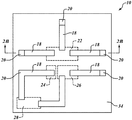
12 フレーム
14 懸架質量部
16 支持梁
18 導電トラック
20 接合パッド
22 集積回路
24 温度センサ
26 ヒータ
28 制御器
30 開口部
Claims (20)
- 開口部を有するフレームと、
前記フレーム上の制御器であって、ヒータを制御するように構成されている制御器と、
熱絶縁材料で作製された複数の支持梁と、
前記フレームの前記開口部に配置された懸架質量部と、
前記懸架質量部上の集積回路、温度センサ、及び前記ヒータと、
前記複数の支持梁の第1の支持梁上の第1の導電トラックと、を備えるデバイスであって、前記懸架質量部は、前記複数の支持梁によって前記フレームに連結し、前記第1の導電トラックは、前記制御器を前記ヒータに電気的に連結する、デバイス。
- 前記複数の支持梁の第2の支持梁上に第2の導電トラックを更に備え、前記第2の導電トラックは、前記制御器を前記温度センサに電気的に連結する、請求項1に記載のデバイス。
- 前記制御器は、前記温度センサから温度測定値を受信し、前記温度測定値に基づいて前記ヒータを制御するように構成されている、請求項2に記載のデバイス。
- 第1のウェハと、
前記フレーム及び前記懸架質量部上の第2のウェハと、を更に備え、前記フレームは前記第1のウェハ上に配置され、前記懸架質量部は前記第1及び前記第2のウェハから離間配置されている、請求項1に記載のデバイス。
- 前記フレーム、前記第1のウェハ、及び前記第2のウェハは、前記懸架質量部の周囲にチェンバを形成する、請求項4に記載のデバイス。
- 前記チェンバは排気されている、請求項5に記載のデバイス。
- 前記第2のウェハを介して形成される導電ビアを更に備え、前記導電ビアは、前記第1の導電トラックに電気的に連結されている、請求項4に記載のデバイス。
- セラミック基部と、
前記セラミック基部に連結する蓋と、を更に備え、前記フレームは前記セラミック基部上に配置され、前記蓋及び前記セラミック基部は、前記懸架質量部の周囲にチェンバを形成する、請求項1に記載のデバイス。
- 前記フレーム上に接合パッドを更に備え、前記第1の導電トラックは、前記接合パッドに電気的に連結している、請求項1に記載のデバイス。
- 基板であって、
開口部を有する第1の部分と、
前記開口部内に配置され、前記第1の部分から離間配置される第2の部分と、を含む基板と、
前記基板の前記第1の部分上の制御器であって、ヒータを制御するように構成されている制御器と、
前記基板の前記第2の部分上の集積回路、温度センサ、及び前記ヒータと、
前記基板の前記第1及び前記第2の部分上の絶縁層であって、前記基板の前記第1及び第2の部分を互いに連結させる前記絶縁層と、
前記絶縁層上の第1の導電トラックと、を備えるデバイスであって、前記第1の導電トラックは、前記制御器を前記ヒータに電気的に連結する、デバイス。
- 前記絶縁層上に第2の導電トラックを更に備え、前記第2の導電トラックは、前記制御器を前記温度センサに電気的に連結する、請求項10に記載のデバイス。
- 前記制御器は、前記温度センサから温度測定値を受信し、前記温度測定値に基づいて前記ヒータを制御するように構成されている、請求項11に記載のデバイス。
- 第1及び第2のウェハを更に備え、前記基板は、前記第1のウェハと前記第2のウェハとの間に配置されている、請求項10に記載のデバイス。
- 気密真空パッケージを更に備え、前記基板は、前記気密真空パッケージの内側に配置されている、請求項10に記載のデバイス。
- 前記基板の前記第1の部分上に接合パッドを更に備え、前記接合パッドは、前記第1の導電トラックに電気的に連結されている、請求項10に記載のデバイス。
- フレームを備える半導体ダイの周辺要素上に制御器を組立てることと、
懸架質量部を備える前記半導体ダイの中心要素上に集積回路、温度センサ、及びヒータ要素を組立てることであって、前記周辺要素は、前記中心要素を取り囲む、ことと、
前記周辺要素と前記中心要素との間にある前記半導体ダイの一部分を取り除くことによって、前記周辺要素から前記中心要素を懸架させることと、
第1の導電トラックを前記半導体ダイと前記懸架させた中心要素を支持する支持梁上に形成することと、を含む、方法であって、前記第1の導電トラックは、前記制御器を前記ヒータ要素に電気的に連結する、方法。
- 前記半導体ダイ上に第2の導電トラックを形成することを更に含み、前記第2の導電トラックは、前記半導体ダイの前記周辺要素上の接合パッドを前記集積回路、前記温度センサ、又は前記ヒータ要素に電気的に連結する、請求項16に記載の方法。
- 前記半導体ダイを第1のウェハ上に配置することと、
前記半導体ダイ上に第2のウェハを配置することと、を更に含み、前記第1のウェハ及び前記第2のウェハは、前記半導体ダイの前記中央要素から離間配置され、前記半導体ダイの前記周辺要素、前記第1のウェハ、及び前記第2のウェハがチェンバを形成する、請求項16に記載の方法。
- 前記チェンバを排気することを更に含む、請求項18に記載の方法。
- 気密真空パッケージに前記半導体ダイを配置することを更に含む、請求項16に記載の方法。
Applications Claiming Priority (2)
| Application Number | Priority Date | Filing Date | Title |
|---|---|---|---|
| US15/099,341 | 2016-04-14 | ||
| US15/099,341 US9607913B1 (en) | 2016-04-14 | 2016-04-14 | Low power, temperature regulated circuit for precision integrated circuits |
Publications (3)
| Publication Number | Publication Date |
|---|---|
| JP2017191102A JP2017191102A (ja) | 2017-10-19 |
| JP2017191102A5 JP2017191102A5 (ja) | 2020-05-14 |
| JP6809973B2 true JP6809973B2 (ja) | 2021-01-06 |
Family
ID=58360120
Family Applications (1)
| Application Number | Title | Priority Date | Filing Date |
|---|---|---|---|
| JP2017078206A Active JP6809973B2 (ja) | 2016-04-14 | 2017-04-11 | 精密集積回路用の低電力温度調節回路 |
Country Status (4)
| Country | Link |
|---|---|
| US (1) | US9607913B1 (ja) |
| EP (1) | EP3232745B1 (ja) |
| JP (1) | JP6809973B2 (ja) |
| CN (1) | CN107301985B (ja) |
Families Citing this family (1)
| Publication number | Priority date | Publication date | Assignee | Title |
|---|---|---|---|---|
| US20230317543A1 (en) * | 2022-04-01 | 2023-10-05 | Fluke Corporation | Structure, system and method for a temperature regulated electrical device |
Family Cites Families (6)
| Publication number | Priority date | Publication date | Assignee | Title |
|---|---|---|---|---|
| DE4340583A1 (de) * | 1993-11-29 | 1995-06-01 | Krautkraemer Gmbh | Temperaturstabilisierter Hybridschaltkreis |
| DE19748005A1 (de) * | 1997-10-30 | 1999-05-20 | Siemens Ag | Anordnung zum Übertragen von elektrischen Signalen zwischen einem auf einer Trägerplatte thermisch isoliertem Modul und angrenzenden Nachbarmodulen |
| US7484411B2 (en) * | 2007-01-30 | 2009-02-03 | Hewlett-Packard Development Company, L.P. | Three phase capacitance-based sensing and actuation |
| US8049326B2 (en) * | 2007-06-07 | 2011-11-01 | The Regents Of The University Of Michigan | Environment-resistant module, micropackage and methods of manufacturing same |
| US7821346B2 (en) * | 2007-08-24 | 2010-10-26 | Cts Corporation | Ovenized oscillator |
| US20100180681A1 (en) * | 2009-01-22 | 2010-07-22 | Honeywell International Inc. | System and method for increased flux density d'arsonval mems accelerometer |
-
2016
- 2016-04-14 US US15/099,341 patent/US9607913B1/en active Active
-
2017
- 2017-04-11 JP JP2017078206A patent/JP6809973B2/ja active Active
- 2017-04-13 EP EP17166640.7A patent/EP3232745B1/en active Active
- 2017-04-14 CN CN201710243779.3A patent/CN107301985B/zh active Active
Also Published As
| Publication number | Publication date |
|---|---|
| JP2017191102A (ja) | 2017-10-19 |
| CN107301985B (zh) | 2022-08-30 |
| US9607913B1 (en) | 2017-03-28 |
| CN107301985A (zh) | 2017-10-27 |
| EP3232745A1 (en) | 2017-10-18 |
| EP3232745B1 (en) | 2020-06-24 |
Similar Documents
| Publication | Publication Date | Title |
|---|---|---|
| US9761543B1 (en) | Integrated circuits with thermal isolation and temperature regulation | |
| US8191792B2 (en) | Temperature sensor, temperature control device, temperature controller and temperature-control method | |
| US10676345B2 (en) | Temperature stabilized MEMS device | |
| TWI557527B (zh) | 具儲熱元件的微機電溫度控制系統 | |
| JP4354347B2 (ja) | 水晶発振器 | |
| KR101447340B1 (ko) | 온도 측정용 장치 | |
| JP6905549B2 (ja) | 熱システム | |
| US10069500B2 (en) | Oven controlled MEMS oscillator | |
| US20190144267A1 (en) | Electronic sensors with sensor die in package structure cavity | |
| JP6809973B2 (ja) | 精密集積回路用の低電力温度調節回路 | |
| KR20170027673A (ko) | 센서 장치 및 센서 장치를 교정하기 위한 방법 | |
| KR101137090B1 (ko) | 가열 가능한 적외선 센서와 이 적외선 센서를 구비하는 적외선 온도계 | |
| US11909354B2 (en) | Ovenized MEMS | |
| US20180131324A1 (en) | High-Efficiency Ovenized Oscillator | |
| US10278281B1 (en) | MEMS stress isolation and stabilization system | |
| KR101469005B1 (ko) | 수정디바이스 및 그 제조 방법 | |
| JP7477371B2 (ja) | 保持装置 | |
| JP2017191102A5 (ja) | ||
| CN110240114B (zh) | 包括微机电系统和封装该微机电系统的盒子的电子系统 | |
| JP2002203661A (ja) | 半導体産業用セラミックヒータの給電端子接続構造 | |
| JP2009232239A (ja) | 恒温型の水晶発振器 | |
| JPH1183593A (ja) | 平型シート状界面センサー | |
| US9899987B2 (en) | Active type temperature compensation resonator structure | |
| JP2010281947A (ja) | 光導波路デバイス | |
| WO2024063652A1 (en) | Thermal processing device and method |
Legal Events
| Date | Code | Title | Description |
|---|---|---|---|
| A521 | Request for written amendment filed |
Free format text: JAPANESE INTERMEDIATE CODE: A523 Effective date: 20200330 |
|
| A621 | Written request for application examination |
Free format text: JAPANESE INTERMEDIATE CODE: A621 Effective date: 20200330 |
|
| TRDD | Decision of grant or rejection written | ||
| A01 | Written decision to grant a patent or to grant a registration (utility model) |
Free format text: JAPANESE INTERMEDIATE CODE: A01 Effective date: 20201201 |
|
| A61 | First payment of annual fees (during grant procedure) |
Free format text: JAPANESE INTERMEDIATE CODE: A61 Effective date: 20201210 |
|
| R150 | Certificate of patent or registration of utility model |
Ref document number: 6809973 Country of ref document: JP Free format text: JAPANESE INTERMEDIATE CODE: R150 |
|
| R250 | Receipt of annual fees |
Free format text: JAPANESE INTERMEDIATE CODE: R250 |