JP6755911B2 - Semiconductor device package - Google Patents
Semiconductor device package Download PDFInfo
- Publication number
- JP6755911B2 JP6755911B2 JP2018165079A JP2018165079A JP6755911B2 JP 6755911 B2 JP6755911 B2 JP 6755911B2 JP 2018165079 A JP2018165079 A JP 2018165079A JP 2018165079 A JP2018165079 A JP 2018165079A JP 6755911 B2 JP6755911 B2 JP 6755911B2
- Authority
- JP
- Japan
- Prior art keywords
- metal body
- groove
- insulating member
- cavity
- region
- Prior art date
- Legal status (The legal status is an assumption and is not a legal conclusion. Google has not performed a legal analysis and makes no representation as to the accuracy of the status listed.)
- Active
Links
Images


Classifications
-
- H—ELECTRICITY
- H01—ELECTRIC ELEMENTS
- H01L—SEMICONDUCTOR DEVICES NOT COVERED BY CLASS H10
- H01L33/00—Semiconductor devices with at least one potential-jump barrier or surface barrier specially adapted for light emission; Processes or apparatus specially adapted for the manufacture or treatment thereof or of parts thereof; Details thereof
- H01L33/48—Semiconductor devices with at least one potential-jump barrier or surface barrier specially adapted for light emission; Processes or apparatus specially adapted for the manufacture or treatment thereof or of parts thereof; Details thereof characterised by the semiconductor body packages
- H01L33/52—Encapsulations
-
- H—ELECTRICITY
- H01—ELECTRIC ELEMENTS
- H01L—SEMICONDUCTOR DEVICES NOT COVERED BY CLASS H10
- H01L33/00—Semiconductor devices with at least one potential-jump barrier or surface barrier specially adapted for light emission; Processes or apparatus specially adapted for the manufacture or treatment thereof or of parts thereof; Details thereof
- H01L33/48—Semiconductor devices with at least one potential-jump barrier or surface barrier specially adapted for light emission; Processes or apparatus specially adapted for the manufacture or treatment thereof or of parts thereof; Details thereof characterised by the semiconductor body packages
- H01L33/64—Heat extraction or cooling elements
- H01L33/647—Heat extraction or cooling elements the elements conducting electric current to or from the semiconductor body
-
- H—ELECTRICITY
- H01—ELECTRIC ELEMENTS
- H01L—SEMICONDUCTOR DEVICES NOT COVERED BY CLASS H10
- H01L33/00—Semiconductor devices with at least one potential-jump barrier or surface barrier specially adapted for light emission; Processes or apparatus specially adapted for the manufacture or treatment thereof or of parts thereof; Details thereof
- H01L33/48—Semiconductor devices with at least one potential-jump barrier or surface barrier specially adapted for light emission; Processes or apparatus specially adapted for the manufacture or treatment thereof or of parts thereof; Details thereof characterised by the semiconductor body packages
- H01L33/62—Arrangements for conducting electric current to or from the semiconductor body, e.g. lead-frames, wire-bonds or solder balls
-
- H—ELECTRICITY
- H01—ELECTRIC ELEMENTS
- H01L—SEMICONDUCTOR DEVICES NOT COVERED BY CLASS H10
- H01L33/00—Semiconductor devices with at least one potential-jump barrier or surface barrier specially adapted for light emission; Processes or apparatus specially adapted for the manufacture or treatment thereof or of parts thereof; Details thereof
- H01L33/48—Semiconductor devices with at least one potential-jump barrier or surface barrier specially adapted for light emission; Processes or apparatus specially adapted for the manufacture or treatment thereof or of parts thereof; Details thereof characterised by the semiconductor body packages
- H01L33/64—Heat extraction or cooling elements
-
- H—ELECTRICITY
- H01—ELECTRIC ELEMENTS
- H01L—SEMICONDUCTOR DEVICES NOT COVERED BY CLASS H10
- H01L2933/00—Details relating to devices covered by the group H01L33/00 but not provided for in its subgroups
- H01L2933/0008—Processes
- H01L2933/0033—Processes relating to semiconductor body packages
-
- H—ELECTRICITY
- H01—ELECTRIC ELEMENTS
- H01L—SEMICONDUCTOR DEVICES NOT COVERED BY CLASS H10
- H01L33/00—Semiconductor devices with at least one potential-jump barrier or surface barrier specially adapted for light emission; Processes or apparatus specially adapted for the manufacture or treatment thereof or of parts thereof; Details thereof
- H01L33/48—Semiconductor devices with at least one potential-jump barrier or surface barrier specially adapted for light emission; Processes or apparatus specially adapted for the manufacture or treatment thereof or of parts thereof; Details thereof characterised by the semiconductor body packages
- H01L33/483—Containers
- H01L33/486—Containers adapted for surface mounting
-
- H—ELECTRICITY
- H01—ELECTRIC ELEMENTS
- H01L—SEMICONDUCTOR DEVICES NOT COVERED BY CLASS H10
- H01L33/00—Semiconductor devices with at least one potential-jump barrier or surface barrier specially adapted for light emission; Processes or apparatus specially adapted for the manufacture or treatment thereof or of parts thereof; Details thereof
- H01L33/48—Semiconductor devices with at least one potential-jump barrier or surface barrier specially adapted for light emission; Processes or apparatus specially adapted for the manufacture or treatment thereof or of parts thereof; Details thereof characterised by the semiconductor body packages
- H01L33/58—Optical field-shaping elements
- H01L33/60—Reflective elements
Description
実施例は半導体素子パッケージに関するものである。 The embodiment relates to a semiconductor device package.
GaN、AlGaNなどの化合物を含む半導体素子は、広くて調整が容易なバンドギャップエネルギーを有するなどの多くの長所を有しているため、発光素子、受光素子および各種ダイオードなどで多様に使用され得る。 Semiconductor devices containing compounds such as GaN and AlGaN have many advantages such as having a wide bandgap energy that can be easily adjusted, and therefore can be widely used in light emitting devices, light receiving elements, various diodes, and the like. ..
特に、半導体の3−5族または2−6族化合物半導体物質を利用した発光ダイオード(Light Emitting Diode)やレーザーダイオード(Laser Diode)のような発光素子は、薄膜成長技術および素子材料の開発により赤色、緑色、青色および紫外線などの多様な色を具現することができ、蛍光物質を利用したり色を組み合わせることによって効率の良い白色光線の具現も可能であり、蛍光灯、白熱灯などの既存の光源と比べて低消費電力、半永久的な寿命、迅速な応答速度、安全性、環境親和性の長所を有する。 In particular, light emitting elements such as light emitting diodes and laser diodes using semiconductor group 3-5 or group 2-6 compound semiconductor materials are red due to thin film growth technology and development of element materials. It is possible to realize various colors such as green, blue and ultraviolet rays, and it is also possible to realize efficient white light by using a diode or combining colors, and existing existing such as fluorescent lamps and incandescent lamps. It has the advantages of low power consumption, semi-permanent life, quick response speed, safety, and environmental friendliness compared to light sources.
それだけでなく、光検出器や太陽電池のような受光素子も、半導体の3−5族または2−6族化合物半導体物質を利用して製作する場合、素子材料の開発により多様な波長領域の光を吸収して光電流を生成することによって、ガンマ線からラジオ波長領域までの多様な波長領域の光を利用することができる。また迅速な応答速度、安全性、環境親和性および素子材料の容易な調節の長所を有するため、電力制御または超高周波回路や通信用モジュールにも容易に利用することができる。 Not only that, when light-receiving elements such as photodetectors and solar cells are also manufactured using semiconductor group 3-5 or group 2-6 compound semiconductor materials, light in various wavelength regions is developed due to the development of element materials. By absorbing light to generate a photocurrent, it is possible to utilize light in various wavelength regions from gamma rays to radio wavelength regions. It also has the advantages of rapid response speed, safety, environmental friendliness and easy adjustment of device materials, so it can be easily used for power control or ultra-high frequency circuits and communication modules.
したがって、半導体素子は、光通信手段の送信モジュール、LCD(Liquid Crystal Display)表示装置のバックライトを構成する冷陰極管(CCFL:Cold Cathode Fluorescence Lamp)を代替する発光ダイオードバックライト、蛍光灯や白熱電球を代替できる白色発光ダイオード照明装置、自動車のヘッドライトおよび信号灯およびGasや火災を感知するセンサなどにまでその応用が拡大している。また、半導体素子は高周波応用回路やその他の電力制御装置、通信用モジュールにまで応用が拡大する可能性がある。 Therefore, the semiconductor element is a transmission module of an optical communication means, a light emitting diode backlight, a fluorescent lamp, or an incandescent lamp that replaces a cold cathode fluorescent lamp (CCFL) that constitutes a backlight of an LCD (Liquid Crystal Display) display device. Its application is expanding to white light emitting diode lighting devices that can replace light bulbs, automobile headlights and signal lights, and sensors that detect Gas and fire. In addition, semiconductor devices may be applied to high-frequency application circuits, other power control devices, and communication modules.
特に、紫外線波長領域の光を放出する発光素子は、硬化作用や殺菌作用をするため、硬化用、医療用、および殺菌用に使用され得る。 In particular, a light emitting element that emits light in the ultraviolet wavelength region can be used for curing, medical use, and sterilization because it has a curing action and a bactericidal action.
最近紫外線発光素子パッケージに関する研究が活発であるが、未だ紫外線発光素子は光抽出効率が相対的に劣る問題があり、内部の熱を外部に効果的に放出できない問題がある。 Recently, research on ultraviolet light emitting element packages has been active, but there is still a problem that ultraviolet light emitting elements have relatively inferior light extraction efficiency, and there is a problem that internal heat cannot be effectively released to the outside.
実施例は熱放出が優秀な半導体素子パッケージを提供する。 The embodiment provides a semiconductor device package with excellent heat release.
実施例は光抽出効率が優秀な半導体素子パッケージを提供する。 The embodiment provides a semiconductor device package having excellent light extraction efficiency.
実施例は、パッケージのカッティング時に発生するバリ(burr)を抑制できる半導体素子パッケージを提供する。 The embodiment provides a semiconductor device package capable of suppressing burrs generated during package cutting.
実施例で解決しようとする課題はこれに限定されるものではなく、下記で説明する課題の解決手段や実施形態から把握され得る目的や効果も含まれるものと言える。 The problem to be solved in the embodiment is not limited to this, and it can be said that the purpose and effect that can be grasped from the solution means and the embodiment of the problem described below are also included.
本発明の一実施例に係る半導体素子パッケージは、第1貫通ホールおよび第2貫通ホールを有する樹脂部;前記樹脂部上に配置され、上面から下面に向かう第1方向に窪んだキャビティを有する導電性胴体;および前記キャビティ内に配置される発光素子;を含み、前記導電性胴体は前記下面から前記第1方向に突出した第1突出部および第2突出部を含み、前記第1突出部は前記第1貫通ホール内に配置され、前記第2突出部は前記第2貫通ホール内に配置され、前記樹脂部の上面は前記導電性胴体の下面に接する。 The semiconductor device package according to an embodiment of the present invention is a resin portion having a first through hole and a second through hole; a conductive cavity arranged on the resin portion and having a cavity recessed in the first direction from the upper surface to the lower surface. The conductive fuselage includes a first projecting portion and a second projecting portion projecting from the lower surface in the first direction, and the first projecting portion includes a sex body; and a light emitting element arranged in the cavity. The second through hole is arranged in the first through hole, the second protruding portion is arranged in the second through hole, and the upper surface of the resin portion is in contact with the lower surface of the conductive body.
前記第1突出部は前記第2突出部より大きくてもよい。 The first protruding portion may be larger than the second protruding portion.
前記第1突出部と第2突出部の面積比は、1:0.2〜1:0.6であり得る。 The area ratio of the first protrusion to the second protrusion can be 1: 0.2 to 1: 0.6.
前記第1突出部および第2突出部はアルミニウムを含むことができる。 The first protrusion and the second protrusion may contain aluminum.
前記導電性胴体は、第1金属パッケージ胴体部、第2金属パッケージ胴体部、および前記第1金属パッケージ胴体部と前記第2金属パッケージ胴体部との間に配置される第1絶縁部材を含むことができる。 The conductive fuselage includes a first metal package fuselage portion, a second metal package fuselage portion, and a first insulating member arranged between the first metal package body portion and the second metal package body portion. Can be done.
前記第1絶縁部材は、前記導電性胴体の複数個の外側面のうち少なくとも2個の外側面に露出され得る。 The first insulating member may be exposed to at least two outer surfaces of the plurality of outer surfaces of the conductive fuselage.
前記第1絶縁部材は前記樹脂部の上面と連結され得る。 The first insulating member may be connected to the upper surface of the resin portion.
前記第1突出部と前記第2突出部との間の間隔は前記第1絶縁部材の幅より大きくてもよい。 The distance between the first protruding portion and the second protruding portion may be larger than the width of the first insulating member.
前記樹脂部と前記第1絶縁部材は互いに異なる物質をそれぞれ具備することができる。 The resin portion and the first insulating member may be provided with different substances.
前記第1金属パッケージ胴体部は、前記第2金属パッケージ胴体部に近づく方向に行くほど厚さが減少して形成される第1陥没部、および前記第1金属パッケージ胴体部の側面と下面の角に形成される第2陥没部を含み、前記第2金属パッケージ胴体部は、前記第1金属パッケージ胴体部に近づく方向に行くほど厚さが減少して形成される第3陥没部、および前記第2金属パッケージ胴体部の側面と下面の角に形成される第4陥没部を含み、前記樹脂部は前記第2陥没部および前記第4陥没部に配置され得る。 The first metal package body portion is formed by reducing the thickness toward the second metal package body portion, and the corners of the side surface and the lower surface of the first metal package body portion. The second metal package body portion includes the second recessed portion formed in the first metal package, and the thickness of the second metal package body portion decreases as the thickness approaches the first metal package body portion. 2. The resin portion may be arranged in the second recessed portion and the fourth depressed portion, including a fourth recessed portion formed at the corners of the side surface and the lower surface of the body portion of the metal package.
前記第1陥没部、第3陥没部、および前記第1絶縁部材は、前記キャビティを形成することができる。 The first depressed portion, the third depressed portion, and the first insulating member can form the cavity.
前記樹脂部の下面は前記第1突出部および第2突出部の下面と面一となり得る。 The lower surface of the resin portion may be flush with the lower surfaces of the first protruding portion and the second protruding portion.
前記第1金属パッケージ胴体部は、複数個の外側面および前記第1絶縁部材と接触する第1接着面を含み、前記第2金属パッケージ胴体部は、複数個の外側面および前記第1絶縁部材と接触する第2接着面を含み、前記第1金属パッケージ胴体部の前記第2陥没部は、前記第1金属パッケージ胴体部の下面と前記第1金属パッケージ胴体部の外側面が会う領域に配置される第1溝、および前記第1金属パッケージ胴体部の下面と第1金属パッケージ胴体部の第1接着面が会う領域に配置される第3溝を含み、前記第2金属パッケージ胴体部の前記第4陥没部は前記第2金属パッケージ胴体部の下面と前記第2金属パッケージ胴体部の外側面が会う領域に配置される第2溝、および前記第2金属パッケージ胴体部の下面と第2金属パッケージ胴体部の接着面が会う領域に配置される第4溝を含み、前記第3溝と前記第4溝は互いに連結され得る。 The first metal package body includes a plurality of outer surfaces and a first adhesive surface in contact with the first insulating member, and the second metal package body includes a plurality of outer surfaces and the first insulating member. The second recessed portion of the first metal package body portion is arranged in a region where the lower surface of the first metal package body portion and the outer surface of the first metal package body portion meet, including the second adhesive surface in contact with the first metal package body portion. The first groove to be formed and the third groove arranged in the area where the lower surface of the first metal package body and the first adhesive surface of the first metal package meet are included. The fourth recessed portion is a second groove arranged in a region where the lower surface of the second metal package body and the outer surface of the second metal package meet, and the lower surface of the second metal package and the second metal. A fourth groove is included in the area where the adhesive surfaces of the package body meet, and the third groove and the fourth groove can be connected to each other.
前記樹脂部は、前記第1溝と前記第2溝に配置される第2絶縁部材、および前記第3溝と前記第4溝に配置される第3絶縁部材を含み、前記第3絶縁部材の幅は前記第1絶縁部材の幅より大きくてもよい。 The resin portion includes the first groove, the second insulating member arranged in the second groove, and the third insulating member arranged in the third groove and the fourth groove, and the third insulating member. The width may be larger than the width of the first insulating member.
前記第2絶縁部材の厚さと前記第3絶縁部材の厚さは互いに異なり得る。 The thickness of the second insulating member and the thickness of the third insulating member may be different from each other.
前記第2絶縁部材の厚さは前記第3絶縁部材の厚さより厚くてもよい。 The thickness of the second insulating member may be thicker than the thickness of the third insulating member.
前記第2絶縁部材の幅は前記第3絶縁部材の幅より小さくてもよい。 The width of the second insulating member may be smaller than the width of the third insulating member.
前記第2絶縁部材の材質と前記第3絶縁部材の材質は同じであり、前記第3絶縁部材と前記第1絶縁部材の材質は互いに異なり得る。 The material of the second insulating member and the material of the third insulating member are the same, and the materials of the third insulating member and the first insulating member may be different from each other.
前記キャビティの内側壁に形成された段差部上に配置される透光部材を含むことができる。 A translucent member arranged on a step portion formed on the inner side wall of the cavity can be included.
前記第1溝の下面の幅と前記第1金属パッケージ胴体部の下面の幅比は、1:3〜1:5であり得る。 The width ratio between the width of the lower surface of the first groove and the width of the lower surface of the first metal package body portion can be 1: 3 to 1: 5.
本発明の他の実施例に係る半導体素子パッケージは、第1金属パッケージ胴体部;前記第1金属パッケージ胴体部と第1絶縁部材によって離隔する第2金属パッケージ胴体部;前記第1金属パッケージ胴体部と前記第2金属パッケージ胴体部に電気的に連結される発光素子;前記第1金属パッケージ胴体部と前記第2金属パッケージ胴体部上に配置される透光部材;を含み、前記第1金属パッケージ胴体部の上部は前記第1金属パッケージ胴体部の厚さの減少により形成される第1陥没部を含み、前記第1金属パッケージ胴体部の下部は複数の外側面に沿って形成される第2陥没部を含み、前記第2金属パッケージ胴体部の上部は前記第2金属パッケージ胴体部の厚さの減少により形成される第3陥没部を含み、前記第2金属パッケージ胴体部の下部は複数の外側面に沿って形成される第4陥没部を含み、前記第1陥没部、前記第3陥没部、前記第1絶縁部材はキャビティを形成し、前記発光素子は前記キャビティ内に配置され、前記第2陥没部と前記第4陥没部に配置される第2絶縁部材を含む。 The semiconductor element package according to another embodiment of the present invention is a first metal package body portion; a second metal package body portion separated from the first metal package body portion by a first insulating member; the first metal package body portion. And a light emitting element electrically connected to the second metal package body; a translucent member arranged on the first metal package body and the second metal package body; the first metal package. The upper portion of the body portion includes a first recessed portion formed by reducing the thickness of the first metal package body portion, and the lower portion of the first metal package body portion is formed along a plurality of outer surfaces. The upper portion of the second metal package body portion includes a recessed portion, the upper portion of the second metal package body portion includes a third recessed portion formed by a decrease in the thickness of the second metal package body portion, and the lower portion of the second metal package body portion includes a plurality of recessed portions. The first depressed portion, the third depressed portion, and the first insulating member form a cavity, and the light emitting element is arranged in the cavity, including a fourth depressed portion formed along the outer side surface. It includes a second recessed portion and a second insulating member arranged in the fourth depressed portion.
実施例によると、半導体素子パッケージの熱放出効率を向上させることができる。 According to the embodiment, the heat release efficiency of the semiconductor device package can be improved.
また、パッケージのカッティング時に発生するバリ(burr)を抑制することができる。 In addition, burrs generated during package cutting can be suppressed.
また、光抽出効率を向上させることができる。 In addition, the light extraction efficiency can be improved.
また、製造工程が簡単となり、製造費用が節減され得る。 In addition, the manufacturing process can be simplified and the manufacturing cost can be reduced.
本発明の多様かつ有益な長所と効果は前述した内容に限定されず、本発明の具体的な実施形態を説明する過程でより容易に理解されるはずである。 The diverse and beneficial advantages and effects of the present invention are not limited to those described above and should be more easily understood in the process of explaining specific embodiments of the present invention.
本実施例は他の形態に変形または複数の実施例を互いに組み合わせることができ、本発明の範囲は以下で説明するそれぞれの実施例に限定されるものではない。 The present embodiment can be modified into other embodiments or a plurality of examples can be combined with each other, and the scope of the present invention is not limited to the respective examples described below.
特定の実施例で説明された事項が他の実施例で説明されていなくても、他の実施例でその事項と反対または矛盾する説明がない限り、他の実施例に関連した説明と理解され得る。 Even if the matter described in a particular embodiment is not explained in another embodiment, it is understood as an explanation related to the other embodiment unless there is an explanation that contradicts or contradicts the matter in the other embodiment. obtain.
例えば、特定の実施例で構成Aに対する特徴を説明し、他の実施例で構成Bに対する特徴を説明したとすれば、構成Aと構成Bが結合された実施例が明示して記載されていなくても反対または矛盾する説明がない限り、本発明の技術的範囲に属するものと理解されるべきである。 For example, if the features for configuration A are explained in a specific embodiment and the features for configuration B are explained in other examples, the embodiment in which configuration A and configuration B are combined is not explicitly described. However, unless there is an opposite or contradictory explanation, it should be understood that it belongs to the technical scope of the present invention.
実施例の説明において、いずれか一つのelementが他のelementの「上(うえ)または下(した)(on or under)」に形成されると記載される場合において、上(うえ)または下(した)(on or under)は、二つのelementが互いに直接(directly)接触するか一つ以上の他のelementが前記両elementの間に配置されて(indirectly)形成されるものをすべて含む。また「上(うえ)または下(した)(on or under)」と表現される場合、一つのelementを基準として上側方向だけでなく下側方向の意味も含み得る。 In the description of the embodiment, when it is described that any one element is formed "on or under" of the other element, the upper or lower (upper) or lower (upper) or lower (on or under). (On or under) includes all those in which two elements are in direct contact with each other or one or more other elements are arranged and formed between the two elements. Further, when the expression "upper" or "lower" is used, it may include not only the upper direction but also the lower direction with respect to one element.
以下、添付した図面を参照して本発明の実施例について、本発明が属する技術分野で通常の知識を有する者が容易に実施できるように詳細に説明する。 Hereinafter, examples of the present invention will be described in detail with reference to the accompanying drawings so that a person having ordinary knowledge in the technical field to which the present invention belongs can easily carry out the embodiments.
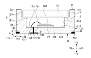
図1は本発明の一実施例に係る半導体素子パッケージの斜視図、図2は本発明の一実施例に係る半導体素子パッケージの平面図であり、図3は本発明の一実施例に係る半導体素子パッケージの断面図、図4は本発明の一実施例に係る半導体素子パッケージの底面図、図5は図3の分解図である。 FIG. 1 is a perspective view of a semiconductor device package according to an embodiment of the present invention, FIG. 2 is a plan view of a semiconductor device package according to an embodiment of the present invention, and FIG. 3 is a plan view of a semiconductor device package according to an embodiment of the present invention. A sectional view of the device package, FIG. 4 is a bottom view of the semiconductor device package according to an embodiment of the present invention, and FIG. 5 is an exploded view of FIG.
図1および図2を参照すると、実施例に係る半導体素子パッケージは、キャビティ11を含む胴体10、キャビティ11の内部に配置される半導体素子100、およびキャビティ11上に配置される透光部材50を含むことができる。
Referring to FIGS. 1 and 2, the semiconductor element package according to the embodiment includes a
胴体10はアルミニウム基板を加工して製作することができる。したがって、実施例に係る胴体10は、内面と外面がすべて導電性を有することができる。このような構造は多様な利点を有することができる。AlN、Al2O3のような非導電性材質を胴体10として使用する場合、紫外線波長帯の反射率が20%〜40%に過ぎないため別途の反射部材を配置しなければならない問題がある。また、リードフレームのような別途の導電性部材および回路パターンが必要となり得る。したがって、製作費用が上昇し工程が複雑となり得る。また、金(Au)のような導電性部材は紫外線を吸収するため光抽出効率が減少する問題がある。
The
しかし、実施例によると、胴体10そのものがアルミニウムで構成されるため紫外線波長帯での反射率が高く、別途の反射部材を省略することができる。また、胴体10自体が導電性があるため、別途の回路パターンおよびリードフレームを省略することができる。また、アルミニウムで製作されるため、熱伝導性が140W/m.k〜160W/m.kと優秀であり得る。したがって、熱放出効率も向上され得る。
However, according to the embodiment, since the
胴体10は、第1金属パッケージ胴体部10aと第2金属パッケージ胴体部10bを含むことができる。第1金属パッケージ胴体部10aと第2金属パッケージ胴体部10bの間には、第1絶縁部材42が配置され得る。第1金属パッケージ胴体部10aと第2金属パッケージ胴体部10bはいずれも導電性を有するため、極を分離するために第1絶縁部材42を配置する必要がある。
The
第1絶縁部材42は絶縁機能を有する多様な材質がすべて含まれ得る。例示的に、第1絶縁部材42はポリイミド(PI)のようなレジンを含むことができるが、必ずしもこれに限定されない。第1絶縁部材42の厚さは10μm〜100μmであり得る。厚さが10μm以上の場合、第1金属パッケージ胴体部10aと第2金属パッケージ胴体部10bを十分に絶縁させることができ、厚さが100μm以下の場合、パッケージのサイズが大きくなる問題を改善することができる。
The first insulating
胴体10は上面から下面に向かう第1方向に窪んだキャビティ11を含むことができる。また、胴体10は上面に配置された第1アライメントマーク15aと第2アライメントマーク15bを含むことができる。第1アライメントマーク15aと第2アライメントマーク15bは互いに異なる形状を有することができる。例示的に、第1アライメントマーク15aは三角形状を有し、第2アライメントマーク15bは四角形状を有することができるが、必ずしもこれに限定されない。
The
胴体10は樹脂部410上に配置され得る。樹脂部410は胴体10の外側面と下面の間の角領域に沿って配置され得る。実施例によると胴体10の下部に樹脂部410が配置されるため、パッケージ切断時にバリ(burr)が発生する問題を改善することができる。
The
第1絶縁部材42は、導電性胴体10の複数個の外側面のうち少なくとも2個の外側面とキャビティ11の底面を貫通することができる。したがって、第1絶縁部材42は胴体10の外側面に露出され得る。
The first insulating
導電性胴体10の外側面と樹脂部410の外側面および第1絶縁部材42の露出面はいずれも同一平面上に配置され得る。すなわち、樹脂部410の外側面と第1絶縁部材42の露出面は、導電性胴体10の外側面と一つの垂直面をなすことができる。
The outer surface of the
第1金属パッケージ胴体部10aは、第2金属パッケージ胴体部10bと向かい合うように配置されてその間に第1絶縁部材42が配置される内側面S14、および胴体10の側面を構成する外側面S11、S12、S13を含むことができる。内側面S24は第1絶縁部材42と接触する第1接着面であり得る。
The first metal
第2金属パッケージ胴体部10bは、第1金属パッケージ胴体部10aと向かい合うように配置されてその間に第1絶縁部材42が配置される内側面S24、および胴体10の側面を構成する外側面S21、S22、S23を含むことができる。内側面S14は第1絶縁部材42と接触する第2接着面であり得る。
The second metal
図3および図4を参照すると、キャビティ11は胴体10の上面に配置されて底面11cと傾斜面11dを有することができる。第1絶縁部材42は胴体の向かい合う2個の外側面を貫通するためキャビティ11の底面11cと傾斜面11dに露出され得る。
With reference to FIGS. 3 and 4, the
第1キャビティ11aの傾斜面11dは底面11cで垂直に配置され得る。しかし、必ずしもこれに限定されず、傾斜面11dは底面11cと90度よりも大きい角度で傾斜して配置されて半導体素子100から出射した光を上部に反射させることができる。前述した通り、胴体10はアルミニウムで製作されるため、キャビティ11の内面は別途の反射部材がなくても紫外線波長帯の光を上部に反射することができる。
The
第2キャビティ11bは第1キャビティ11aの上部に配置され、透光部材50が配置され得る直径を有することができる。透光部材50は第1キャビティ11aと第2キャビティ11bの間の段差部15に支持され得る。第2キャビティ11bは外周面から胴体10の角に向かって突出した複数個のリセス17を含むことができる。
The
胴体10は、下面12と側面13が会う角に配置される第1、第2溝14a、14b、および第1、第2溝14a、14bに配置される第2絶縁部材41a、41bを含むことができる。第1、第2溝14a、14bは胴体10の下面12と側面13が会う角領域に沿って全体的に配置され得る。
The
具体的には、胴体10は第1金属パッケージ胴体部10aの下面12aと外側面S21、S22、S23が会う領域に配置される第1溝14a、第2金属パッケージ胴体部10bの下面12bと外側面S11、S12、S13が会う領域に配置される第2溝14bを含むことができる。
Specifically, the
第2絶縁部材41a、41bは第1溝14aに配置される第2−1絶縁部41aと第2溝14bに配置される第2−2絶縁部41bを含むことができる。この時、第2−1絶縁部41aと第2−2絶縁部41bは一体に形成され得る。
The second insulating
第1溝14aと第2溝14bの形状は特に制限しない。第1溝14aと第2溝14bの断面は多角形状、レンズ形状などをすべて含むことができる。
The shapes of the
第2絶縁部材41a、41bは第1絶縁部材42と同一材質であり得る。第1絶縁部材42と第2絶縁部材41a、41bは、EMC、ホワイトシリコン、PSR(Photoimageable Solder Resist)、シリコーン樹脂組成物、シリコーン変性エポキシ樹脂などの変性エポキシ樹脂組成物、エポキシ変性シリコーン樹脂などの変性シリコーン樹脂組成物、ポリイミド樹脂組成物、変性ポリイミド樹脂組成物、ポリフタルアミド(PPA)、ポリカーボネート樹脂、ポリフェニレンサルファイド(PPS)、液晶ポリマー(LCP)、ABS樹脂、フェノール樹脂、アクリル樹脂、PBT樹脂などの樹脂などが選択され得る。
The second insulating
しかし、これに限定されず、第1絶縁部材42の材質は第2絶縁部材41a、41bの材質と異なってもよい。例示的に、第1絶縁部材42はポリイミド(PI)系列の接着物質を含むことができる。したがって、第1絶縁部材42は第2絶縁部材41a、41bより耐熱性が優秀な物質を含むことができる。
However, the material is not limited to this, and the material of the first insulating
この場合、第1絶縁部材42の生成時に形成される高温、高圧の環境や、共晶(eutectic)、銀ペースト(Ag paste)等のダイボンディング(die bonding)工程時に形成される約320℃に達する高温の環境においても、第1絶縁部材42が壊れたり割れることを抑制することができる。
In this case, the temperature is set to about 320 ° C., which is formed in a high-temperature, high-pressure environment formed when the first insulating
実施例によると、胴体10の下角に第2絶縁部材41a、41bが配置されるため、パッケージの切削時に角にバリ(burr)が発生することを防止することができる。アルミニウム基板の場合、金属材質であるので切削時にバリ(burr)がよく発生する可能性がある。バリ(burr)が発生した場合、下面12が平坦でないため回路基板への実装が不良となり得る。また、バリ(burr)が発生した場合、厚さが不均一となり得、一部の領域に浮きが発生して測定誤差が発生し得る。第2絶縁部材41a、41bは絶縁材質で製作されるので、切削時にバリ(burr)の発生が抑制され得る。
According to the embodiment, since the second insulating
第1溝14aと第2溝14bの内面は粗さ(図示されず)を有することができる。第1溝14aと第2溝14bの内面がなめらかな場合、第2絶縁部材41a、41bとの接着力が弱くなり得る。したがって、第2絶縁部材41a、41bを固定するために第1溝14aと第2溝14bの内面は表面処理を通じて粗さを形成することができる。
The inner surfaces of the
第2絶縁部材41a、41bの第1方向厚さ(Y方向幅、d1)は50μm〜150μmであり得る。第1方向(Y方向)は、胴体10の下面から上面の方向であり得る。厚さが50μm以上の場合、十分な厚さを確保してパッケージ切断時にバリ(burr)が発生することを防止することができ、厚さが150μm以下の場合、第2絶縁部材41a、41bが胴体10の下面12に突出することを防止することができる。
The thickness (Y direction width, d1) of the second insulating
第2絶縁部材41a、41bの第2方向幅(X方向幅、w1)は100μm〜300μmであり得る。第2方向(X方向)は第1方向と垂直な方向であり得る。幅が100μm以上の場合、第1溝14aと第2溝14bに十分に固定され得、幅が300μm以下の場合、胴体10の下面12に電極が実装される面積を確保することができる。
The width in the second direction (width in the X direction, w1) of the second insulating
実施例によると、第2絶縁部材41a、41bの厚さと幅比d1:w1は1:1.5〜1:6であり得る。すなわち、第2絶縁部材41a、41bの幅は厚さより大きくてもよい。厚さと幅比を満足する場合、第2絶縁部材41a、41bが第1溝14に十分に固定されてバリ(burr)の発生を抑制することができる。
According to the embodiment, the thickness and width ratio d1: w1 of the second insulating
胴体10は第1金属パッケージ胴体部10aの下面12aと内側面S24が会う領域に配置される第3溝19a、第2金属パッケージ胴体部10bの下面12bおよび内側面S14が会う角領域に配置される第4溝19b、および第3溝19aと第4溝19bに配置される第3絶縁部材43を含むことができる。
The
第3絶縁部材43は胴体10の下面12に配置されて第2絶縁部材41a、41bおよび第1絶縁部材42と連結され得る。また、第1方向(Y方向)に第3絶縁部材43は第1絶縁部材42と重なり得る。この時、第1方向(Y方向)に第1絶縁部材42の長さは第3絶縁部材43の長さより長くてもよい。
The third insulating
第1溝〜第4溝14a、14b、19a、19bは同時に形成され得る。また、第2絶縁部材41a、41bと第3絶縁部材43は一回のコーティング工程によって形成され得る。したがって、第3絶縁部材43の材質は第2絶縁部材41a、41bと同じであり得るが、必ずしもこれに限定されない。
The first groove to the
第1金属パッケージ胴体部10aの下面12a、第2金属パッケージ胴体部10bの下面12b、第2絶縁部材41a、41bの下面および第3絶縁部材43の下面は同一平面上に配置され得る。すなわち、第2絶縁部材41a、41bと第3絶縁部材43は胴体10の下面12より突出しないため、全体として平坦面を形成することができる。したがって、回路基板に実装時に不良率が減少しパッケージの厚さを減らすことができる。
The
第3絶縁部材43の厚さ(Y方向幅、d2)は10μm〜100μmであり得る。厚さが10μm以上の場合、第2溝19に十分に固定され得、厚さが100μm以下の場合、第2溝19の深さを低く制御できるため半導体素子100が実装される領域の厚さを確保することができる。半導体素子が実装される領域は、キャビティ11が形成されて胴体10のうち厚さが最も薄い領域であるため、できる限り第2溝19の深さを浅く形成することが有利であり得る。
The thickness (Y direction width, d2) of the third insulating
第3絶縁部材43の幅(X方向幅、w2)は300μm〜700μmであり得る。幅が300μm以上の場合、電極面12a、12bの間を十分に離隔させてショートを防止することができ、幅が700μm以下の場合、胴体10の下面12に電極が実装される十分な面積を確保することができる。したがって、第3絶縁部材43の幅w2は第2絶縁部材41a、41bの幅w1より大きくてもよい。
The width (width in the X direction, w2) of the third insulating
第2絶縁部材41a、41bの厚さd1は第3絶縁部材43の厚さd2より厚くてもよい。半導体素子100が実装される領域はキャビティ11が形成されて胴体10のうち厚さが最も薄い領域であるため、できる限り第2溝19の深さを浅く形成することが有利であり得る。また、第2絶縁部材41a、41bはバリ(burr)を防止するために所定の厚さを有することができる。その結果、第2絶縁部材41a、41bの厚さd1が第3絶縁部材43の厚さd2より大きい場合、バリ(burr)が発生することを効果的に防止しながらもパッケージの強度を確保することができる。
The thickness d1 of the second insulating
しかし、必ずしもこれに限定されず、第2絶縁部材41a、41bの厚さd1は第3絶縁部材43の厚さd2と同じであってもよい。
However, the thickness d1 of the second insulating
前述した通り、胴体10は導電性を有するため、第1金属パッケージ胴体部の下面12aと第2金属パッケージ胴体部の下面12bはそれぞれ伝導性を有することができる。この時、第2絶縁部材41a、41bは角に沿って配置されて第1金属パッケージ胴体部の下面12aと第2金属パッケージ胴体部の下面12bを取り囲み、第3絶縁部材43は第1金属パッケージ胴体部の下面12aと第2金属パッケージ胴体部の下面12bの間に配置され得る。第3絶縁部材43の長さ方向に両終端は第2絶縁部材41a、41bに接することができる。
As described above, since the
第1金属パッケージ胴体部の下面12aは第2金属パッケージ胴体部の下面12bより広くてもよい。第1金属パッケージ胴体部の下面12aと第2金属パッケージ胴体部の下面12bの面積比は、1:0.2〜1:0.6であり得る。面積比が1:0.2以上の場合、第2金属パッケージ胴体部の下面12bの面積が確保されてショートを防止することができ、面積比が1:0.6以下の場合、第1金属パッケージ胴体部の下面12aの上部にサブマウントを配置する空間を確保することができる。
The
第1溝の下面の幅w1と第1金属パッケージ胴体部の下面の幅w4の比w1:w4は、1:3〜1:5であり得る。幅比が1:3以上の場合、第1金属パッケージ胴体部の下面12aの面積が増加してサブマウントが装着される面積を確保することができ、幅比が1:5以下の場合、第2絶縁部材の幅が増加してバリ(burr)の発生を効果的に抑制することができる。
The ratio w1: w4 of the width w1 of the lower surface of the first groove and the width w4 of the lower surface of the first metal package body portion can be 1: 3 to 1: 5. When the width ratio is 1: 3 or more, the area of the
第3溝の下面の幅w21と第1溝の下面の幅w1の比w21:w4は、1:0.8〜1:1.2であり得る。すなわち、第3絶縁部材43の幅w2は第2絶縁部材41a、41bの幅w1より2倍以上大きくてもよい。したがって、第1金属パッケージ胴体部と第2金属パッケージ胴体部の下面12a、12bを十分に離隔させてショートを防止することができる。
The ratio w21: w4 of the width w21 of the lower surface of the third groove to the width w1 of the lower surface of the first groove can be 1: 0.8 to 1: 1.2. That is, the width w2 of the third insulating
胴体10の上面には第4絶縁部材44が配置され得る。第4絶縁部材44は第1、第2絶縁部材42、41と同じ材質であってもよく異なる材質であってもよい。第4絶縁部材44の厚さは第2絶縁部材41a、41bより薄くてもよい。
A fourth insulating
半導体素子100はキャビティ11内に配置され得る。半導体素子100は第1金属パッケージ胴体部10aおよび第2金属パッケージ胴体部10bと電気的に連結され得る。キャビティ11にはサブマウント22が配置され、その上に半導体素子100が配置され得る。キャビティ11の底にはワイヤーがボンディングされるパッド部(図示されず)が配置され得る。
The
半導体素子100は紫外線波長帯の光を出力することができる。例示的に、半導体素子100は近紫外線波長帯の光UV−Aを出力してもよく、遠紫外線波長帯の光UV−Bを出力してもよく、深紫外線波長帯の光UV−Cを出力してもよい。波長範囲は発光構造物120のAlの組成比によって決定され得る。
The
例示的に、近紫外線波長帯の光UV−Aは320nm〜390nm範囲でピーク波長を有することができ、遠紫外線波長帯の光UV−Bは280nm〜320nm範囲でピーク波長を有することができ、深紫外線波長帯の光UV−Cは100nm〜280nm範囲でピーク波長を有することができる。 Illustratively, light UV-A in the near-ultraviolet wavelength band can have a peak wavelength in the range of 320 nm to 390 nm, and light UV-B in the far-ultraviolet wavelength band can have a peak wavelength in the range of 280 nm to 320 nm. Light UV-C in the deep ultraviolet wavelength band can have a peak wavelength in the range of 100 nm to 280 nm.
透光部材50はキャビティ11上に配置され得る。透光部材50は第1キャビティ11aと第2キャビティ11bの間に配置される段差部15に支持され得る。段差部15と透光部材50の間には接着層(図示されず)が配置され得る。接着層が過充填された場合、余分の接着剤はリセス17に後退し得る。したがって、接着剤が過度に塗布されても透光部材50の水平を維持することができる。
The
透光部材50は紫外線波長帯の光を透過できる材質であれば特に制限しない。例示的に、透過層はクォーツ(Quartz)のように紫外線波長透過率の高い光学材料を含むことができるが、これに限定されるものではない。
The
図5を参照すると、胴体10は樹脂部410上に配置され得る。すなわち、樹脂部410の上面410aは胴体10の下面と接することができる。樹脂部410は上面410aと下面410bを貫通する第1貫通ホール411と第2貫通ホール412を含むことができる。
With reference to FIG. 5, the
胴体10は、下面に突出して第1貫通ホール411に配置される第1突出部12a−1および下面に突出して第2貫通ホール412に配置される第2突出部12b−1を含むことができる。したがって、第1突出部12a−1の下面12a、第2突出部12b−1の下面12b、および樹脂部410の下面410bは同一平面上に配置され得る。第1、第2突出部12a−1、12a−2の材質は、胴体10と同じアルミニウム材質であり得る。
The
第1貫通ホール411は第2貫通ホール412より大きくてもよい。したがって、第1突出部12a−1の大きさは第2突出部12b−1の大きさより大きくてもよい。
The first through
第1突出部12a−1と第2突出部12b−1の面積比は、1:0.2〜1:0.6であり得る。面積比が1:0.2以上の場合、第2突出部12b−1の面積が確保されてショートを防止することができ、面積比が1:0.6以下の場合、第1突出部12a−1の上部にサブマウントを配置する空間を確保することができる。
The area ratio of the first protruding
第1突出部12a−1と第2突出部12b−1の間の間隙W2は、第1絶縁部材42の幅より大きくてもよい。したがって、第1突出部12a−1と第2突出部12b−1の間に配置される第3絶縁部材43の幅が広くなりョートが防止され得る。
The gap W2 between the first protruding
第1金属パッケージ胴体部10aは、第2金属パッケージ胴体部10bに近づく方向(X2方向)に行くほど厚さが減少して形成される第1陥没部11−1、および第1金属パッケージ胴体部10aの側面S21、S22、S23、S24と下面12aが会う角領域に形成される第2陥没部14a、19aを含むことができる。
The thickness of the first metal
第2金属パッケージ胴体部10bは、第1金属パッケージ胴体部10aに近づく方向(X1方向)に行くほど厚さが減少して形成される第2陥没部11−2、および第2金属パッケージ胴体部10bの側面S11、S12、S13、S14と下面12bが会う角領域に形成される第4陥没部14b、19bを含むことができる。第1陥没部11−1、第2陥没部11−2、および第1絶縁部材42の上面は胴体のキャビティ11を形成することができる。
The thickness of the second metal
第1金属パッケージ胴体部10aの第2陥没部14a、19aは、第1金属パッケージ胴体部10aの下面12aと第1金属パッケージ胴体部10aの外側面S21、S22、S23が会う領域に配置される第1溝14a、および第1金属パッケージ胴体部10aの下面12aと第1金属パッケージ胴体部10aの第1接着面S24が会う領域に配置される第3溝19aを含むことができる。
The second recessed
第2金属パッケージ胴体部10bの第4陥没部14b、19bは、第2金属パッケージ胴体部10bの下面12bと外側面S11、S12、S13が会う領域に配置される第2溝14b、および第2金属パッケージ胴体部10bの下面12bと第2金属パッケージ胴体部10bの第2接着面S14が会う領域に配置される第4溝19bを含むことができる。この時、第3溝19aと第4溝19bは互いに連結され得る。
The fourth recessed
樹脂部410は第1溝14aと第2溝14bに配置される第2絶縁部材41a、41b、および第3溝19aと第4溝19bに配置される第3絶縁部材43を含むことができる。したがって、樹脂部410は前述した第2絶縁部材41a、41bと第3絶縁部材43の特徴をすべて含むことができる。
The
すなわち、第2絶縁部材41a、41bの厚さは第3絶縁部材43の厚さより厚くてもよく、第2絶縁部材41a、41bの幅は第3絶縁部材43の幅より小さくてもよい。
That is, the thickness of the second insulating
また、第2絶縁部材41a、41bと第3絶縁部材43の材質は第1絶縁部材42の材質と異なってもよい。
Further, the materials of the second insulating
第2絶縁部材41a、41bの幅W1は胴体上面の幅W5より小さくてもよい。第2絶縁部材41a、41bの幅W1は胴体上面の幅W5の50%〜90%であり得る。このような構造によると、胴体の下部に電極を実装する面積を十分に確保しながらも第2絶縁部材41a、41bの幅を確保して胴体10との付着力を確保することができる。
The width W1 of the second insulating
図6aは本発明の一実施例に係る半導体素子の概念図であり、図6bは図6aの変形例である。 FIG. 6a is a conceptual diagram of a semiconductor device according to an embodiment of the present invention, and FIG. 6b is a modification of FIG. 6a.
図6aを参照すると、実施例に係る半導体素子100はサブマウント22上にフリップチップのように実装され得る。すなわち、半導体素子100の第1電極152と第2電極151がサブマウント22の第1パッド23aと第2パッド23bにフリップチップの形態で実装され得る。この時、第1パッド23aと第2パッド23bはワイヤーWにより胴体10にそれぞれソルダリングされ得る。
With reference to FIG. 6a, the
しかし、半導体素子100を実装する方法は特に制限しない。例示的に、図6のように半導体素子の基板110をサブマウント22上に配置して第1電極152と第2電極151を直接胴体10にソルダリングしてもよい。
However, the method of mounting the
実施例に係る半導体素子は、基板110、第1導電型半導体層120、活性層130、および第2導電型半導体層140を含むことができる。各半導体層は紫外線波長帯の光を放出することができるようにアルミニウム組成を有することができる。
The semiconductor element according to the embodiment can include a
基板110は導電性基板または絶縁性基板を含む。基板110は半導体物質の成長に適合した物質であるかキャリアウェハーであり得る。基板110はサファイア(Al2O3)、SiC、GaAs、GaN、ZnO、Si、GaP、InPおよびGeのうち選択された物質で形成され得、これに対して限定しはしない。必要に応じて基板110は除去され得る。
The
第1導電型半導体層120と基板110の間にはバッファー層(図示されず)がさらに備えられ得る。バッファー層は基板110上に備えられた発光構造物160と基板110の格子不整合を緩和することができる。
A buffer layer (not shown) may be further provided between the first
第1導電型半導体層120はIII−V族、II−VI族などの化合物半導体で具現され得、第1導電型半導体層120に第1ドーパントがドーピングされ得る。第1導電型半導体層120は、Inx1Aly1Ga1−x1−y1N(0≦x1≦1、0≦y1≦1、0≦x1+y1≦1)の組成式を有する半導体材料、例えばGaN、AlGaN、InGaN、InAlGaNなどで選択され得る。そして、第1ドーパントはSi、Ge、Sn、Se、Teのようなn型ドーパントであり得る。第1ドーパントがn型ドーパントである場合、第1ドーパントがドーピングされた第1導電型半導体層120はn型半導体層であり得る。
The first
活性層130は第1導電型半導体層120を介して注入される電子(または正孔)と第2導電型半導体層140を介して注入される正孔(または電子)が会う層である。活性層130は電子と正孔が再結合するにつれて低いエネルギー準位に遷移し、それに相応する波長を有する光を生成することができる。
The
活性層130は、単一井戸構造、多重井戸構造、単一量子井戸構造、多重量子井戸(Multi Quantum Well;MQW)構造、量子ドット構造または量子細線構造のうちいずれか一つの構造を有することができ、活性層130の構造はこれに限定されない。
The
第2導電型半導体層140は活性層130上に形成され、III−V族、II−VI族などの化合物半導体で具現され得、第2導電型半導体層140に第2ドーパントがドーピングされ得る。第2導電型半導体層140は、Inx5Aly2Ga1−x5−y2N(0≦x5≦1、0≦y2≦1、0≦x5+y2≦1)の組成式を有する半導体物質またはAlInN、AlGaAs、GaP、GaAs、GaAsP、AlGaInPのうち選択された物質で形成され得る。第2ドーパントがMg、Zn、Ca、Sr、Baなどのようなp型ドーパントである場合、第2ドーパントがドーピングされた第2導電型半導体層140はp型半導体層であり得る。
The second
第1電極152は第1導電型半導体層120と電気的に連結され得、第2電極151は第2導電型半導体層140と電気的に連結され得る。第1および第2電極152、151は、Ti、Ru、Rh、Ir、Mg、Zn、Al、In、Ta、Pd、Co、Ni、Si、Ge、AgおよびAuとこれらの選択的な合金の中で選択され得る。
The
実施例では水平型発光素子の構造で説明したが、必ずしもこれに限定されない。例示的に、実施例に係る発光素子は垂直型またはフリップチップ構造でもよい。 In the examples, the structure of the horizontal light emitting element has been described, but the present invention is not necessarily limited to this. Illustratively, the light emitting element according to the embodiment may have a vertical type or a flip chip structure.
図7は本発明の他の実施例に係る半導体素子パッケージの断面図、図8は本発明のさらに他の実施例に係る半導体素子パッケージの断面図、図9は図1の変形例である。 FIG. 7 is a cross-sectional view of a semiconductor device package according to another embodiment of the present invention, FIG. 8 is a cross-sectional view of a semiconductor device package according to still another embodiment of the present invention, and FIG. 9 is a modification of FIG.
図7を参照すると、第1絶縁部材42は下面12の中央に配置されてもよい。すなわち、サブマウントが省略された構造では第1絶縁部材42の位置は自由に変更され得る。この時、第1金属パッケージ胴体部10aと第2金属パッケージ胴体部10bは、互いに対称となる形状を有してもよい。
With reference to FIG. 7, the first insulating
図8を参照すると、第2絶縁部材41は胴体10の側面13から遠ざかるほど厚さが小さくなり得る。このような構成によると、胴体10の側面13で第2絶縁部材41a、41bの厚さが厚いため、パッケージ切断時にバリ(burr)の発生を効果的に抑制することができる。また、胴体の下面12を最大限に確保することができるため、胴体10の下面12に電極が実装される面積を十分に確保することができる。しかし、必ずしもこれに限定されず、第2絶縁部材41a、41bは胴体10の側面13から遠ざかるほど連続的に厚さが減少するのではなく階段式に厚さが減少してもよい。
Referring to FIG. 8, the thickness of the second insulating
胴体10の側面13には第5絶縁部45が配置されてもよい。第5絶縁部45は胴体10の上面に配置された第4絶縁部と連結され得る。実施例に係る胴体10はアルミニウムで製作されるため、外部の静電気(ESD)等に脆弱であり得る。第4絶縁部材44と第5絶縁部45は胴体10の外面に配置されて外観を保護し、静電気(ESD)およびショート(Short)を防止することができる。
A fifth insulating
第5絶縁部45の厚さは10μm〜100μmであり得る。第5絶縁部45の厚さが10μmより小さい場合、胴体10の外面を十分に絶縁することが困難であり得、厚さが100μmより大きい場合、パッケージのサイズが大きくなる問題がある。
The thickness of the fifth insulating
しかし、必ずしもこれに限定されず、第5絶縁部45は胴体10の外面を酸化させて形成することができる。胴体10の外面を酸化させる方法は特に制限しない。例示的に、チャンバー内で酸素を供給して外面を酸化させることができる。しかし、必ずしもこれに限定されず、アルミニウムの表面を酸化させる多様な表面処理技術が適用され得る。
However, the present invention is not necessarily limited to this, and the fifth insulating
この時、胴体10の内面と下面は酸化しないようにマスク処理することができる。下面と内面は半導体素子100に電流を供給するチャネルとして機能する可能性があるためである。また、キャビティ11の内面が酸化する場合、紫外線光に対する反射率が低下する問題がある。
At this time, the inner surface and the lower surface of the
図9を参照すると、透光部材50は胴体10の上面に配置され得る。この場合、胴体10の上面に直接透光部材50が配置される場合は接着が困難であり得る。胴体10の上面は相対的に粗さが小さいためである。したがって、実施例によると、胴体10の上面に第4絶縁部材44を形成して粗さを増加させた後、その上に接着剤51を塗布して透光部材50を固定することができる。しかし、必ずしもこれに限定されず、第4絶縁部材は省略されてもよい。
With reference to FIG. 9, the
図10a〜図10eは、本発明の一実施例に係る半導体素子パッケージの製造過程を示す図面である。 10a to 10e are drawings showing a manufacturing process of a semiconductor device package according to an embodiment of the present invention.
図10aを参照すると、複数個のアルミニウム基板10−1の間に第1絶縁部材42を塗布して接合することができる。第1絶縁部材42は絶縁機能を有する多様な材質がすべて含まれ得る。第1絶縁部材42の厚さは10μm〜100μmであり得る。厚さが10μm以上の場合、複数個のアルミニウム基板10−1を十分に絶縁させることができない可能性があり、厚さが100μm以下の場合、パッケージのサイズが大きくなる問題を改善することができる。
With reference to FIG. 10a, the first insulating
図10bを参照すると、複数個のアルミニウム基板10−1に複数個のキャビティ11を形成することができる。キャビティ11は、半導体素子が配置される第1キャビティ11aと透光部材50が配置される第2キャビティ11bを共に形成することができる。キャビティ11を形成する方法は特に限定しない。例示的に、一般的な金属加工方法をすべて適用することができる。
With reference to FIG. 10b, a plurality of
この時、アルミニウム基板の下面12に複数個の溝14、19を形成することができる。その後、図10cを参照すると、複数個の溝14、19に第2絶縁部材41と第3絶縁部材43をコーティングすることもできる。この場合、工程が単純化され、第2絶縁部材41と第3絶縁部材43が一体に形成されて接着力が優秀となり得る。
At this time, a plurality of
図10dを参照すると、キャビティ11内に半導体素子100を実装し、その上に透光部材50を固定することができる。透光部材50を別途の接着剤を利用して固定することができる。
With reference to FIG. 10d, the
半導体素子100はキャビティ11内に配置され得る。キャビティ11にはサブマウントが配置され、その上に半導体素子100が配置され得る。キャビティ11の底にはワイヤーがボンディングされるパッド部(図示されず)が配置され得る。
The
半導体素子100は紫外線波長帯の光を出力することができる。例示的に、半導体素子100は近紫外線波長帯の光UV−Aを出力してもよく、遠紫外線波長帯の光UV−Bを出力してもよく、深紫外線波長帯の光UV−Cを出力してもよい。波長範囲は発光構造物120のAlの組成比によって決定され得る。
The
透光部材50は紫外線波長帯の光を透過できる材質であれば特に制限しない。例示的に、透過層はクォーツ(Quartz)のように紫外線波長透過率の高い光学材料を含むことができるが、これに限定されるものではない。
The
その後、胴体10の上面に第4絶縁部材44を形成することができる。第4絶縁部材44の厚さは特に限定しない。また、必要に応じて胴体10の側面13に第5絶縁部を形成することができる。
After that, the fourth insulating
実施例に係る第1〜第5絶縁部41、42、43、44、45は、EMC、ホワイトシリコン、PSR(Photoimageable Solder Resist)、シリコーン樹脂組成物、シリコーン変性エポキシ樹脂などの変性エポキシ樹脂組成物、エポキシ変性シリコーン樹脂などの変性シリコーン樹脂組成物、ポリイミド樹脂組成物、変性ポリイミド樹脂組成物、ポリフタルアミド(PPA)、ポリカーボネート樹脂、ポリフェニレンサルファイド(PPS)、液晶ポリマー(LCP)、ABS樹脂、フェノール樹脂、アクリル樹脂、PBT樹脂などの樹脂等で形成され得る。しかし、必ずしもこれに限定されない。
The first to fifth insulating
図10eを参照すると、複数個のアルミニウム基板10−1を複数個に切断して複数個のパッケージを製作することができる。この時、切断面は第2絶縁部材41が配置された領域を通過することができる。前述した通り、切断時に終端に第2絶縁部材41が配置されるため、バリ(burr)が抑制され得る。
With reference to FIG. 10e, a plurality of packages can be manufactured by cutting a plurality of aluminum substrates 10-1 into a plurality of pieces. At this time, the cut surface can pass through the region where the second insulating
半導体素子は多様な種類の光源装置に適用され得る。例示的に、光源装置は殺菌装置、硬化装置、照明装置、および表示装置および車両用ランプなどを含む概念であり得る。すなわち、半導体素子はケースに配置されて光を提供する多様な電子デバイスに適用され得る。 Semiconductor devices can be applied to various types of light source devices. Illustratively, a light source device can be a concept that includes a sterilizer, a curing device, a lighting device, and a display device, a vehicle lamp, and the like. That is, semiconductor devices can be applied to a variety of electronic devices that are placed in a case to provide light.
殺菌装置は実施例に係る半導体素子を具備して所望する領域を殺菌することができる。殺菌装置は、浄水器、エアコン、冷蔵庫などの生活家電に適用され得るが必ずしもこれに限定されない。すなわち、殺菌装置は殺菌が必要な多様な製品(例:医療機器)にすべて適用され得る。 The sterilizer is provided with the semiconductor element according to the embodiment and can sterilize a desired region. The sterilizer can be applied to, but is not limited to, household appliances such as water purifiers, air conditioners, and refrigerators. That is, the sterilizer can be applied to all various products that require sterilization (eg, medical devices).
例示的に、浄水器は循環する水を殺菌するために、実施例に係る殺菌装置を具備することができる。殺菌装置は水が循環するノズルまたは吐出口に配置されて紫外線を照射することができる。この時、殺菌装置は防水構造を含むことができる。 Illustratively, a water purifier can be equipped with a sterilizer according to an embodiment for sterilizing circulating water. The sterilizer can be placed in a nozzle or outlet where water circulates to irradiate ultraviolet light. At this time, the sterilizer may include a waterproof structure.
硬化装置は実施例に係る半導体素子を具備して多様な種類の液体を硬化させることができる。液体は紫外線が照射されると硬化する多様な物質をすべて含む最広義の概念であり得る。例示的に、硬化装置は多様な種類のレジンを硬化させることができる。または硬化装置はマニキュアのような美容製品の硬化に適用されてもよい。 The curing device includes the semiconductor element according to the embodiment and can cure various kinds of liquids. Liquids can be the broadest concept that includes all the various substances that cure when exposed to UV light. Illustratively, a curing device can cure a wide variety of resins. Alternatively, the curing device may be applied to cure beauty products such as nail polish.
照明装置は、基板と実施例の半導体素子を含む光源モジュール、光源モジュールの熱を発散させる放熱部および外部から提供された電気的信号を処理または変換して光源モジュールに提供する電源提供部を含むことができる。また、照明装置は、ランプ、ヘッドランプ、または街路灯などを含むことができる。 The lighting device includes a light source module including a substrate and a semiconductor element of the embodiment, a heat radiating unit that dissipates heat from the light source module, and a power supply unit that processes or converts an electrical signal provided from the outside and provides the light source module. be able to. The lighting device can also include lamps, headlamps, street lights, and the like.
表示装置はボトムカバー、反射板、発光モジュール、導光板、光学シート、ディスプレイパネル、画像信号出力回路およびカラーフィルターを含むことができる。ボトムカバー、反射板、発光モジュール、導光板および光学シートはバックライトユニット(Backlight Unit)を構成することができる。 Display devices can include bottom covers, reflectors, light emitting modules, light guide plates, optical sheets, display panels, image signal output circuits and color filters. The bottom cover, the reflector, the light emitting module, the light guide plate, and the optical sheet can form a backlight unit (Backlight Unit).
反射板はボトムカバー上に配置され、発光モジュールは光を放出することができる。導光板は反射板の前方に配置されて発光モジュールから発散する光を前方に案内し、光学シートはプリズムシートなどを含んで構成されて導光板の前方に配置され得る。ディスプレイパネルは光学シートの前方に配置され、画像信号出力回路はディスプレイパネルに画像信号を供給し、カラーフィルターはディスプレイパネルの前方に配置され得る。 The reflector is placed on the bottom cover and the light emitting module can emit light. The light guide plate is arranged in front of the reflector to guide the light emitted from the light emitting module to the front, and the optical sheet may be configured to include a prism sheet or the like and be arranged in front of the light guide plate. The display panel may be placed in front of the optical sheet, the image signal output circuit may supply the image signal to the display panel, and the color filter may be placed in front of the display panel.
半導体素子は、表示装置のバックライトユニットとして使用される際に、エッジタイプのバックライトユニットとして使用されるか直下タイプのバックライトユニットとして使用され得る。 When the semiconductor element is used as a backlight unit of a display device, it can be used as an edge type backlight unit or a direct type backlight unit.
半導体素子は前述した発光ダイオードの他にレーザーダイオードでもよい。 The semiconductor element may be a laser diode in addition to the light emitting diode described above.
レーザーダイオードは、発光素子と同様に、前述した構造の第1導電型半導体層と活性層および第2導電型半導体層を含むことができる。そして、p−型の第1導電型半導体とn−型の第2導電型半導体を接合させた後、電流を流した時に光が放出されるelectro−luminescence(電界発光)現象を利用するが、放出される光の方向性と位相において差がある。すなわち、レーザーダイオードは励起放出(stimulated emission)という現象と補強干渉現象などを利用して、一つの特定の波長(単色光、monochromatic beam)を有する光が同一位相を有して同一方向に放出され得、このような特性によって光通信や医療用装備および半導体工程装備などに使用され得る。 Similar to the light emitting element, the laser diode may include a first conductive semiconductor layer, an active layer, and a second conductive semiconductor layer having the above-mentioned structure. Then, after joining the p-type first conductive type semiconductor and the n-type second conductive type semiconductor, the electro-luminescence (electroluminescence) phenomenon in which light is emitted when an electric current is passed is used. There is a difference in the direction and phase of the emitted light. That is, the laser diode utilizes a phenomenon called stimulated emission and a reinforcing interference phenomenon to emit light having one specific wavelength (monochromatic light, monochromatic beam) in the same phase and in the same direction. Due to such characteristics, it can be used for optical communication, medical equipment, semiconductor process equipment, and the like.
受光素子としては、光を検出してその強度を電気信号に変換する一種のトランスデューサーである光検出器(photodetector)を例に挙げることができる。このような光検出器として、光電池(シリコン、セレン)、光出力導素子(硫化カドミウム、セレン化カドミウム)、フォトダイオード(例えば、visible blind spectral regionやtrue blind spectral regionでピーク波長を有するPD)、フォトトランジスタ、光電子増倍管、光電管(真空、ガス封入)、IR(Infra−Red)検出器などがあるが、実施例はこれに限定されない。 As an example of the light receiving element, a photodetector, which is a kind of transducer that detects light and converts its intensity into an electric signal, can be mentioned as an example. Such photodetectors include photovoltaic cells (silicon, selenium), light output conductors (cadmium sulfide, cadmium selenium), photodiodes (eg, PDs having peak wavelengths in visible blend spectral region and true blend spectral region). Examples include, but are not limited to, photomultiplier tubes, photomultiplier tubes, phototubes (vacuum, gas filled), IR (Infra-Red) detectors, and the like.
また、光検出器のような半導体素子は、一般的に光変換効率が優秀な直接遷移半導体(direct bandgap semiconductor)を利用して製作され得る。または光検出器は構造が多様であり、最も一般的な構造としては、p−n接合を利用するpin型光検出器と、ショットキー接合(Schottky junction)を利用するショットキー型光検出器と、MSM(Metal Semiconductor Metal)型光検出器などがある。 Further, a semiconductor element such as a photodetector can be manufactured by using a direct bandgap semiconductor, which is generally excellent in optical conversion efficiency. Alternatively, the photodetector has various structures, and the most common structures are a pin-type photodetector that uses a pn junction and a Schottky-type photodetector that uses a Schottky junction. , MSM (Metal-Semiconductor Metal) type photodetector and the like.
フォトダイオード(Photodiode)は発光素子と同様に、前述した構造の第1導電型半導体層と活性層および第2導電型半導体層を含むことができ、pn接合またはpin構造からなる。フォトダイオードは逆バイアスあるいはゼロバイアスを加えて動作するようになり、光がフォトダイオードに入射すると電子と正孔が生成されて電流が流れる。この時、電流の大きさはフォトダイオードに入射する光の強度に略比例し得る。 Like the light emitting element, the photodiode can include a first conductive semiconductor layer, an active layer, and a second conductive semiconductor layer having the above-mentioned structure, and has a pn junction or a pin structure. The photodiode operates with a reverse bias or zero bias, and when light enters the photodiode, electrons and holes are generated and a current flows. At this time, the magnitude of the current can be substantially proportional to the intensity of the light incident on the photodiode.
光電池または太陽電池(solar cell)はフォトダイオードの一種であって、光を電流に変換することができる。太陽電池は、発光素子と同様に、前述した構造の第1導電型半導体層と活性層および第2導電型半導体層を含むことができる。 A photovoltaic cell or a solar cell is a type of photodiode that can convert light into an electric current. Similar to the light emitting element, the solar cell can include a first conductive semiconductor layer, an active layer, and a second conductive semiconductor layer having the above-mentioned structure.
また、p−n接合を利用した一般的なダイオードの整流特性を通じて、電子回路の整流器として利用されてもよく、超高周波回路に適用されて発振回路などに適用されてもよい。 Further, it may be used as a rectifier of an electronic circuit through the rectifying characteristics of a general diode using a pn junction, or may be applied to an ultra-high frequency circuit and applied to an oscillation circuit or the like.
また、前述した半導体素子は必ずしも半導体のみで具現されず、場合により金属物質をさらに含むこともできる。例えば、受光素子のような半導体素子は、Ag、Al、Au、In、Ga、N、Zn、Se、P、またはAsのうち少なくとも一つを利用して具現され得、p型やn型ドーパントによってドーピングされた半導体物質や真性半導体物質を利用して具現されてもよい。 Further, the above-mentioned semiconductor element is not necessarily embodied only by a semiconductor, and may further contain a metallic substance in some cases. For example, a semiconductor device such as a light receiving element can be embodied by utilizing at least one of Ag, Al, Au, In, Ga, N, Zn, Se, P, or As, and is a p-type or n-type dopant. It may be embodied by utilizing a semiconductor material or an intrinsic semiconductor material doped with.
以上、実施例を中心に説明したがこれは単に例示に過ぎず、本発明を限定するものではなく、本発明が属する分野の通常の知識を有する者であれば、本実施例の本質的な特性を逸脱しない範囲で、以上で例示されていない多様な変形と応用が可能であることが分かるはずである。例えば、実施例に具体的に示された各構成要素は変形して実施できるものである。そして、このような変形と応用に関連した差異点は添付された特許請求の範囲で規定する本発明の範囲に含まれると解釈されるべきである。
Although the examples have been mainly described above, this is merely an example and does not limit the present invention, and any person who has ordinary knowledge in the field to which the present invention belongs is essential to the present embodiment. It should be seen that a variety of modifications and applications not illustrated above are possible without departing from the properties. For example, each component specifically shown in the examples can be modified and implemented. And, it should be interpreted that the difference related to such modification and application is included in the scope of the present invention specified in the appended claims.
Claims (6)
前記キャビティ内に配置される発光素子と、
前記金属胴体の底面に配置され、第1貫通ホールおよび第2貫通ホールを含む樹脂部と、
前記金属胴体上に配置される透光部材と、を含み、
前記金属胴体は、第1金属胴体と、第2金属胴体と、前記第1金属胴体と前記第2金属胴体との間に配置される絶縁部材と、を含み、
前記第1金属胴体の一部、前記第2金属胴体の一部、および、前記絶縁部材の一部は、前記キャビティの底面に位置し、
前記発光素子は、前記第1金属胴体の一部および前記第2金属胴体の一部と電気的に連結され、
前記第1金属胴体および前記第2金属胴体それぞれは、前記金属胴体の底面から突出した第1突出部および第2突出部をそれぞれ含み、
前記金属胴体は、前記第1突出部および前記第2突出部と前記絶縁部材との間の第1領域と、前記第1突出部および前記第2突出部と前記キャビティの底面とが垂直に重なる第2領域と、前記キャビティの外側に配置されて前記金属胴体の最上部面と重なる第3領域と、を含み、
前記第1領域の厚さは前記第2領域の厚さより薄く、
前記第2領域の厚さは前記第3領域の厚さより薄く、
前記第3領域は、前記キャビティから最も遠い領域の厚さが、前記キャビティから最も近い領域の厚さより薄く、
前記第1突出部および前記第2突出部は、前記第1貫通ホールおよび前記第2貫通ホール内にそれぞれ配置され、
前記第1突出部は前記第2突出部より大きく、
前記発光素子は紫外線光を出射し、前記第1突出部および前記第2突出部はアルミニウムを含み、
前記金属胴体は、前記第1金属胴体および前記第2金属胴体の底面に設置されている第1溝と、前記第1突出部と前記第2突出部との間に設置されている第2溝と、を含み、
前記第1溝は前記金属胴体の周辺に沿って閉ループ形状に形成されて前記第1金属胴体および前記第2金属胴体の底面が露出し、
前記第2溝は両終端が前記第1溝と連結され、
前記第1溝および前記第2溝には前記樹脂部が配置され、
前記第2溝の水平方向の幅は前記絶縁部材の水平方向の幅より大きく、
前記第1溝および前記第2溝に配置された樹脂部の材質は前記絶縁部材の材質と異なる、発光素子パッケージ。 A metal body including a cavity containing a bottom contact and side walls,
A light emitting element arranged in the cavity and
A resin portion arranged on the bottom surface of the metal body and including the first through hole and the second through hole, and
Anda light transmitting member arranged on the metal body,
The metal body includes a first metal body, and a second metal body, and an insulating member disposed between the front Symbol first metal body and the second metal body,
The first metal body part, part of the second metal body, and a portion of the insulating member is located on the bottom surface of the cavity,
The light emitting element is partially electrically connected in the second metal body and contact a portion of the first metal body,
Wherein the first metal body and the second metal body each comprise a first protruding portion protruding from the bottom surface of the metal body and the second projecting portions respectively,
The metal body includes a first region between the first projecting portion and the second projecting portion and the insulating member, and the first projecting portion and the second projecting portion and the bottom surface of the cavity overlaps the vertical Includes a second region and a third region that is located outside the cavity and overlaps the top surface of the metal fuselage .
The thickness of the first region is thinner than the thickness of the second region.
The thickness of the second region is thinner than the thickness of the third region.
In the third region, the thickness of the region farthest from the cavity is thinner than the thickness of the region closest to the cavity.
The first projecting portion and the second projecting portion is disposed to each of the first through-hole and the second through-hole,
The first protrusion is larger than the second protrusion,
The light emitting element emits ultraviolet light, and the first protrusion and the second protrusion contain aluminum.
The metal body has a first groove installed on the bottom surface of the first metal body and the second metal body, and a second groove installed between the first protrusion and the second protrusion. And, including
The first groove is formed in a closed loop shape along the periphery of the metal body, and the bottom surfaces of the first metal body and the second metal body are exposed.
Both ends of the second groove are connected to the first groove.
The resin portion is arranged in the first groove and the second groove.
The horizontal width of the second groove is larger than the horizontal width of the insulating member.
A light emitting element package in which the material of the resin portion arranged in the first groove and the second groove is different from the material of the insulating member .
Applications Claiming Priority (4)
| Application Number | Priority Date | Filing Date | Title |
|---|---|---|---|
| KR10-2017-0113439 | 2017-09-05 | ||
| KR20170113439 | 2017-09-05 | ||
| KR1020180101576A KR102641336B1 (en) | 2017-09-05 | 2018-08-28 | Semiconductor device package |
| KR10-2018-0101576 | 2018-08-28 |
Publications (3)
| Publication Number | Publication Date |
|---|---|
| JP2019047123A JP2019047123A (en) | 2019-03-22 |
| JP2019047123A5 JP2019047123A5 (en) | 2019-06-13 |
| JP6755911B2 true JP6755911B2 (en) | 2020-09-16 |
Family
ID=65761758
Family Applications (1)
| Application Number | Title | Priority Date | Filing Date |
|---|---|---|---|
| JP2018165079A Active JP6755911B2 (en) | 2017-09-05 | 2018-09-04 | Semiconductor device package |
Country Status (5)
| Country | Link |
|---|---|
| US (1) | US11335843B2 (en) |
| JP (1) | JP6755911B2 (en) |
| KR (1) | KR102641336B1 (en) |
| CN (1) | CN109427946B (en) |
| TW (1) | TWI802587B (en) |
Families Citing this family (4)
| Publication number | Priority date | Publication date | Assignee | Title |
|---|---|---|---|---|
| KR102650690B1 (en) * | 2018-10-23 | 2024-03-25 | 주식회사 루멘스 | Ultraviolet light emitting diode package |
| WO2021014904A1 (en) * | 2019-07-25 | 2021-01-28 | 株式会社大真空 | Lid material for light-emitting device, method for manufacturing lid material, and light-emitting device |
| JP7370274B2 (en) | 2020-02-18 | 2023-10-27 | 日機装株式会社 | Semiconductor packages and semiconductor light emitting devices |
| JP7450466B2 (en) * | 2020-06-22 | 2024-03-15 | スタンレー電気株式会社 | Light-emitting device and method for manufacturing the light-emitting device |
Family Cites Families (33)
| Publication number | Priority date | Publication date | Assignee | Title |
|---|---|---|---|---|
| JP4003866B2 (en) * | 2001-12-04 | 2007-11-07 | シチズン電子株式会社 | Surface mount type light emitting diode and manufacturing method thereof |
| JP2003304000A (en) | 2002-04-08 | 2003-10-24 | Citizen Electronics Co Ltd | Method for manufacturing package for light-emitting diode |
| KR100593943B1 (en) | 2005-04-30 | 2006-06-30 | 삼성전기주식회사 | Method for manufacturing light emitting diode package |
| US8044418B2 (en) * | 2006-07-13 | 2011-10-25 | Cree, Inc. | Leadframe-based packages for solid state light emitting devices |
| JP4205135B2 (en) | 2007-03-13 | 2009-01-07 | シャープ株式会社 | Semiconductor light emitting device, multiple lead frame for semiconductor light emitting device |
| JP5326705B2 (en) | 2009-03-17 | 2013-10-30 | 日亜化学工業株式会社 | Light emitting device |
| JP5367668B2 (en) | 2009-11-17 | 2013-12-11 | スタンレー電気株式会社 | Light emitting device and manufacturing method thereof |
| KR101157530B1 (en) | 2009-12-16 | 2012-06-22 | 인탑스엘이디 주식회사 | LED Package And the Method for producing The same |
| JP5383611B2 (en) | 2010-01-29 | 2014-01-08 | 株式会社東芝 | LED package |
| TW201250964A (en) * | 2011-01-27 | 2012-12-16 | Dainippon Printing Co Ltd | Resin-attached lead frame, method for manufacturing same, and lead frame |
| KR101852388B1 (en) | 2011-04-28 | 2018-04-26 | 엘지이노텍 주식회사 | Light emitting device package |
| CN103078040B (en) | 2011-08-22 | 2016-12-21 | Lg伊诺特有限公司 | Light emitting device packaging piece and electro-optical device |
| JP6015231B2 (en) | 2011-08-26 | 2016-10-26 | 大日本印刷株式会社 | LED element mounting substrate, method for manufacturing the same, and semiconductor device using the LED element mounting substrate |
| KR101853067B1 (en) * | 2011-08-26 | 2018-04-27 | 엘지이노텍 주식회사 | Light emitting device package |
| US9263658B2 (en) * | 2012-03-05 | 2016-02-16 | Seoul Viosys Co., Ltd. | Light-emitting device and method of manufacturing the same |
| KR101400271B1 (en) | 2012-08-03 | 2014-05-28 | (주)포인트엔지니어링 | method for manufacturing light emitting device and the device thereby |
| KR101373710B1 (en) | 2012-12-12 | 2014-03-13 | (주)포인트엔지니어링 | Led metal substrate and method for manufacturing the substrate |
| CN104103734B (en) * | 2013-04-02 | 2017-03-01 | 展晶科技(深圳)有限公司 | Package structure for LED |
| KR20150001268A (en) | 2013-06-27 | 2015-01-06 | 엘지이노텍 주식회사 | Light emitting device package |
| US9583689B2 (en) * | 2013-07-12 | 2017-02-28 | Lite-On Opto Technology (Changzhou) Co., Ltd. | LED package |
| KR101541035B1 (en) | 2013-08-16 | 2015-08-03 | (주)포인트엔지니어링 | Chip substrate for preventing burr generating and method for manufacturing the same |
| DE102014102810A1 (en) | 2014-03-04 | 2015-09-10 | Osram Opto Semiconductors Gmbh | Production of optoelectronic components |
| DE102014103034A1 (en) | 2014-03-07 | 2015-09-10 | Osram Opto Semiconductors Gmbh | Optoelectronic component and method for its production |
| WO2015148185A1 (en) | 2014-03-25 | 2015-10-01 | 3M Innovative Properties Company | Flexible circuits with coplanar conductive features and methods of making same |
| JP6185415B2 (en) | 2014-03-27 | 2017-08-23 | 株式会社東芝 | Semiconductor light emitting device |
| EP3975272A1 (en) * | 2014-05-29 | 2022-03-30 | Suzhou Lekin Semiconductor Co., Ltd. | Light emitting device package |
| CN104037316B (en) | 2014-06-19 | 2017-06-20 | 鸿利智汇集团股份有限公司 | A kind of LED inorganic encapsulateds support and its method for packing |
| CN106663731B (en) | 2014-08-05 | 2019-08-06 | 西铁城电子株式会社 | Semiconductor device and its manufacturing method |
| KR20160038568A (en) * | 2014-09-30 | 2016-04-07 | (주)포인트엔지니어링 | Chip substrate comprising plural curve surface cavity |
| KR101668353B1 (en) * | 2014-11-03 | 2016-10-21 | (주)포인트엔지니어링 | Chip substrate and chip package module |
| JP6765804B2 (en) * | 2014-11-28 | 2020-10-07 | エルジー イノテック カンパニー リミテッド | Light emitting element package |
| US10211378B2 (en) * | 2016-01-29 | 2019-02-19 | Nichia Corporation | Light emitting device and method for manufacturing same |
| US9893250B1 (en) * | 2016-12-16 | 2018-02-13 | Nichia Corporation | Light emitting device having silicone resin-based sealing member |
-
2018
- 2018-08-28 KR KR1020180101576A patent/KR102641336B1/en active IP Right Grant
- 2018-08-31 US US16/119,469 patent/US11335843B2/en active Active
- 2018-09-04 JP JP2018165079A patent/JP6755911B2/en active Active
- 2018-09-04 TW TW107131008A patent/TWI802587B/en active
- 2018-09-05 CN CN201811034004.6A patent/CN109427946B/en active Active
Also Published As
| Publication number | Publication date |
|---|---|
| CN109427946B (en) | 2022-05-20 |
| KR102641336B1 (en) | 2024-02-28 |
| JP2019047123A (en) | 2019-03-22 |
| TW201921728A (en) | 2019-06-01 |
| TWI802587B (en) | 2023-05-21 |
| US20190074422A1 (en) | 2019-03-07 |
| CN109427946A (en) | 2019-03-05 |
| US11335843B2 (en) | 2022-05-17 |
| KR20190026581A (en) | 2019-03-13 |
Similar Documents
| Publication | Publication Date | Title |
|---|---|---|
| EP3483944B1 (en) | Light emitting device package and lighting apparatus comprising same | |
| JP6755911B2 (en) | Semiconductor device package | |
| KR20190006889A (en) | Light emitting device package | |
| US11355674B2 (en) | Semiconductor device package | |
| EP3451396A1 (en) | Semiconductor device package | |
| KR102472710B1 (en) | Semiconductor device package | |
| KR102537080B1 (en) | Semiconductor device package | |
| KR102509075B1 (en) | Semiconductor device package | |
| KR102509089B1 (en) | Semiconductor device package | |
| KR102531150B1 (en) | Optical lens and semiconductor device package | |
| KR102607890B1 (en) | Semiconductor device package | |
| KR102518578B1 (en) | Semiconductor device package and lighting device module including the same | |
| KR102432034B1 (en) | Semiconductor device package | |
| US11715817B2 (en) | Light-emitting element package and light-emitting element module including same | |
| KR102644793B1 (en) | Light emitting device package | |
| KR102401827B1 (en) | Light emitting device package and lighting apparatus | |
| US20200357967A1 (en) | Semiconductor device package and light emitting device comprising same | |
| KR20200077180A (en) | Light emitting device package | |
| KR20190094721A (en) | Semiconductor device package and light emitting device including the same | |
| KR20190094719A (en) | Semiconductor device package and light emitting device including the same | |
| KR20190094723A (en) | Semiconductor device package and light emitting device including the same | |
| KR20190094720A (en) | Semiconductor device package and light emitting device including the same | |
| KR20190014323A (en) | Light emitting device package and manufacturing method of light emitting device package |
Legal Events
| Date | Code | Title | Description |
|---|---|---|---|
| A521 | Request for written amendment filed |
Free format text: JAPANESE INTERMEDIATE CODE: A523 Effective date: 20190510 |
|
| A621 | Written request for application examination |
Free format text: JAPANESE INTERMEDIATE CODE: A621 Effective date: 20190510 |
|
| A871 | Explanation of circumstances concerning accelerated examination |
Free format text: JAPANESE INTERMEDIATE CODE: A871 Effective date: 20190510 |
|
| A975 | Report on accelerated examination |
Free format text: JAPANESE INTERMEDIATE CODE: A971005 Effective date: 20190821 |
|
| A131 | Notification of reasons for refusal |
Free format text: JAPANESE INTERMEDIATE CODE: A131 Effective date: 20190827 |
|
| A977 | Report on retrieval |
Free format text: JAPANESE INTERMEDIATE CODE: A971007 Effective date: 20190828 |
|
| A601 | Written request for extension of time |
Free format text: JAPANESE INTERMEDIATE CODE: A601 Effective date: 20191125 |
|
| A521 | Request for written amendment filed |
Free format text: JAPANESE INTERMEDIATE CODE: A523 Effective date: 20200124 |
|
| A131 | Notification of reasons for refusal |
Free format text: JAPANESE INTERMEDIATE CODE: A131 Effective date: 20200324 |
|
| A521 | Request for written amendment filed |
Free format text: JAPANESE INTERMEDIATE CODE: A523 Effective date: 20200623 |
|
| TRDD | Decision of grant or rejection written | ||
| A01 | Written decision to grant a patent or to grant a registration (utility model) |
Free format text: JAPANESE INTERMEDIATE CODE: A01 Effective date: 20200811 |
|
| A61 | First payment of annual fees (during grant procedure) |
Free format text: JAPANESE INTERMEDIATE CODE: A61 Effective date: 20200826 |
|
| R150 | Certificate of patent or registration of utility model |
Ref document number: 6755911 Country of ref document: JP Free format text: JAPANESE INTERMEDIATE CODE: R150 |
|
| S111 | Request for change of ownership or part of ownership |
Free format text: JAPANESE INTERMEDIATE CODE: R313113 |
|
| R350 | Written notification of registration of transfer |
Free format text: JAPANESE INTERMEDIATE CODE: R350 |
|
| R250 | Receipt of annual fees |
Free format text: JAPANESE INTERMEDIATE CODE: R250 |