JP6753769B2 - Image driving method of organic light emitting display device, organic light emitting display panel, organic light emitting display device, and organic light emitting diode deterioration sensing driving method of organic light emitting display device - Google Patents
Image driving method of organic light emitting display device, organic light emitting display panel, organic light emitting display device, and organic light emitting diode deterioration sensing driving method of organic light emitting display device Download PDFInfo
- Publication number
- JP6753769B2 JP6753769B2 JP2016245319A JP2016245319A JP6753769B2 JP 6753769 B2 JP6753769 B2 JP 6753769B2 JP 2016245319 A JP2016245319 A JP 2016245319A JP 2016245319 A JP2016245319 A JP 2016245319A JP 6753769 B2 JP6753769 B2 JP 6753769B2
- Authority
- JP
- Japan
- Prior art keywords
- line
- light emitting
- organic light
- subpixel
- gate
- Prior art date
- Legal status (The legal status is an assumption and is not a legal conclusion. Google has not performed a legal analysis and makes no representation as to the accuracy of the status listed.)
- Active
Links
Images


Classifications
-
- G—PHYSICS
- G09—EDUCATION; CRYPTOGRAPHY; DISPLAY; ADVERTISING; SEALS
- G09G—ARRANGEMENTS OR CIRCUITS FOR CONTROL OF INDICATING DEVICES USING STATIC MEANS TO PRESENT VARIABLE INFORMATION
- G09G3/00—Control arrangements or circuits, of interest only in connection with visual indicators other than cathode-ray tubes
- G09G3/20—Control arrangements or circuits, of interest only in connection with visual indicators other than cathode-ray tubes for presentation of an assembly of a number of characters, e.g. a page, by composing the assembly by combination of individual elements arranged in a matrix no fixed position being assigned to or needed to be assigned to the individual characters or partial characters
- G09G3/22—Control arrangements or circuits, of interest only in connection with visual indicators other than cathode-ray tubes for presentation of an assembly of a number of characters, e.g. a page, by composing the assembly by combination of individual elements arranged in a matrix no fixed position being assigned to or needed to be assigned to the individual characters or partial characters using controlled light sources
- G09G3/30—Control arrangements or circuits, of interest only in connection with visual indicators other than cathode-ray tubes for presentation of an assembly of a number of characters, e.g. a page, by composing the assembly by combination of individual elements arranged in a matrix no fixed position being assigned to or needed to be assigned to the individual characters or partial characters using controlled light sources using electroluminescent panels
- G09G3/32—Control arrangements or circuits, of interest only in connection with visual indicators other than cathode-ray tubes for presentation of an assembly of a number of characters, e.g. a page, by composing the assembly by combination of individual elements arranged in a matrix no fixed position being assigned to or needed to be assigned to the individual characters or partial characters using controlled light sources using electroluminescent panels semiconductive, e.g. using light-emitting diodes [LED]
- G09G3/3208—Control arrangements or circuits, of interest only in connection with visual indicators other than cathode-ray tubes for presentation of an assembly of a number of characters, e.g. a page, by composing the assembly by combination of individual elements arranged in a matrix no fixed position being assigned to or needed to be assigned to the individual characters or partial characters using controlled light sources using electroluminescent panels semiconductive, e.g. using light-emitting diodes [LED] organic, e.g. using organic light-emitting diodes [OLED]
- G09G3/3275—Details of drivers for data electrodes
- G09G3/3291—Details of drivers for data electrodes in which the data driver supplies a variable data voltage for setting the current through, or the voltage across, the light-emitting elements
-
- G—PHYSICS
- G09—EDUCATION; CRYPTOGRAPHY; DISPLAY; ADVERTISING; SEALS
- G09G—ARRANGEMENTS OR CIRCUITS FOR CONTROL OF INDICATING DEVICES USING STATIC MEANS TO PRESENT VARIABLE INFORMATION
- G09G3/00—Control arrangements or circuits, of interest only in connection with visual indicators other than cathode-ray tubes
- G09G3/20—Control arrangements or circuits, of interest only in connection with visual indicators other than cathode-ray tubes for presentation of an assembly of a number of characters, e.g. a page, by composing the assembly by combination of individual elements arranged in a matrix no fixed position being assigned to or needed to be assigned to the individual characters or partial characters
- G09G3/22—Control arrangements or circuits, of interest only in connection with visual indicators other than cathode-ray tubes for presentation of an assembly of a number of characters, e.g. a page, by composing the assembly by combination of individual elements arranged in a matrix no fixed position being assigned to or needed to be assigned to the individual characters or partial characters using controlled light sources
- G09G3/30—Control arrangements or circuits, of interest only in connection with visual indicators other than cathode-ray tubes for presentation of an assembly of a number of characters, e.g. a page, by composing the assembly by combination of individual elements arranged in a matrix no fixed position being assigned to or needed to be assigned to the individual characters or partial characters using controlled light sources using electroluminescent panels
- G09G3/32—Control arrangements or circuits, of interest only in connection with visual indicators other than cathode-ray tubes for presentation of an assembly of a number of characters, e.g. a page, by composing the assembly by combination of individual elements arranged in a matrix no fixed position being assigned to or needed to be assigned to the individual characters or partial characters using controlled light sources using electroluminescent panels semiconductive, e.g. using light-emitting diodes [LED]
- G09G3/3208—Control arrangements or circuits, of interest only in connection with visual indicators other than cathode-ray tubes for presentation of an assembly of a number of characters, e.g. a page, by composing the assembly by combination of individual elements arranged in a matrix no fixed position being assigned to or needed to be assigned to the individual characters or partial characters using controlled light sources using electroluminescent panels semiconductive, e.g. using light-emitting diodes [LED] organic, e.g. using organic light-emitting diodes [OLED]
- G09G3/3225—Control arrangements or circuits, of interest only in connection with visual indicators other than cathode-ray tubes for presentation of an assembly of a number of characters, e.g. a page, by composing the assembly by combination of individual elements arranged in a matrix no fixed position being assigned to or needed to be assigned to the individual characters or partial characters using controlled light sources using electroluminescent panels semiconductive, e.g. using light-emitting diodes [LED] organic, e.g. using organic light-emitting diodes [OLED] using an active matrix
- G09G3/3233—Control arrangements or circuits, of interest only in connection with visual indicators other than cathode-ray tubes for presentation of an assembly of a number of characters, e.g. a page, by composing the assembly by combination of individual elements arranged in a matrix no fixed position being assigned to or needed to be assigned to the individual characters or partial characters using controlled light sources using electroluminescent panels semiconductive, e.g. using light-emitting diodes [LED] organic, e.g. using organic light-emitting diodes [OLED] using an active matrix with pixel circuitry controlling the current through the light-emitting element
-
- G—PHYSICS
- G09—EDUCATION; CRYPTOGRAPHY; DISPLAY; ADVERTISING; SEALS
- G09G—ARRANGEMENTS OR CIRCUITS FOR CONTROL OF INDICATING DEVICES USING STATIC MEANS TO PRESENT VARIABLE INFORMATION
- G09G3/00—Control arrangements or circuits, of interest only in connection with visual indicators other than cathode-ray tubes
- G09G3/20—Control arrangements or circuits, of interest only in connection with visual indicators other than cathode-ray tubes for presentation of an assembly of a number of characters, e.g. a page, by composing the assembly by combination of individual elements arranged in a matrix no fixed position being assigned to or needed to be assigned to the individual characters or partial characters
- G09G3/22—Control arrangements or circuits, of interest only in connection with visual indicators other than cathode-ray tubes for presentation of an assembly of a number of characters, e.g. a page, by composing the assembly by combination of individual elements arranged in a matrix no fixed position being assigned to or needed to be assigned to the individual characters or partial characters using controlled light sources
- G09G3/30—Control arrangements or circuits, of interest only in connection with visual indicators other than cathode-ray tubes for presentation of an assembly of a number of characters, e.g. a page, by composing the assembly by combination of individual elements arranged in a matrix no fixed position being assigned to or needed to be assigned to the individual characters or partial characters using controlled light sources using electroluminescent panels
- G09G3/32—Control arrangements or circuits, of interest only in connection with visual indicators other than cathode-ray tubes for presentation of an assembly of a number of characters, e.g. a page, by composing the assembly by combination of individual elements arranged in a matrix no fixed position being assigned to or needed to be assigned to the individual characters or partial characters using controlled light sources using electroluminescent panels semiconductive, e.g. using light-emitting diodes [LED]
- G09G3/3208—Control arrangements or circuits, of interest only in connection with visual indicators other than cathode-ray tubes for presentation of an assembly of a number of characters, e.g. a page, by composing the assembly by combination of individual elements arranged in a matrix no fixed position being assigned to or needed to be assigned to the individual characters or partial characters using controlled light sources using electroluminescent panels semiconductive, e.g. using light-emitting diodes [LED] organic, e.g. using organic light-emitting diodes [OLED]
- G09G3/3225—Control arrangements or circuits, of interest only in connection with visual indicators other than cathode-ray tubes for presentation of an assembly of a number of characters, e.g. a page, by composing the assembly by combination of individual elements arranged in a matrix no fixed position being assigned to or needed to be assigned to the individual characters or partial characters using controlled light sources using electroluminescent panels semiconductive, e.g. using light-emitting diodes [LED] organic, e.g. using organic light-emitting diodes [OLED] using an active matrix
- G09G3/3258—Control arrangements or circuits, of interest only in connection with visual indicators other than cathode-ray tubes for presentation of an assembly of a number of characters, e.g. a page, by composing the assembly by combination of individual elements arranged in a matrix no fixed position being assigned to or needed to be assigned to the individual characters or partial characters using controlled light sources using electroluminescent panels semiconductive, e.g. using light-emitting diodes [LED] organic, e.g. using organic light-emitting diodes [OLED] using an active matrix with pixel circuitry controlling the voltage across the light-emitting element
-
- G—PHYSICS
- G09—EDUCATION; CRYPTOGRAPHY; DISPLAY; ADVERTISING; SEALS
- G09G—ARRANGEMENTS OR CIRCUITS FOR CONTROL OF INDICATING DEVICES USING STATIC MEANS TO PRESENT VARIABLE INFORMATION
- G09G2300/00—Aspects of the constitution of display devices
- G09G2300/04—Structural and physical details of display devices
- G09G2300/0421—Structural details of the set of electrodes
- G09G2300/043—Compensation electrodes or other additional electrodes in matrix displays related to distortions or compensation signals, e.g. for modifying TFT threshold voltage in column driver
-
- G—PHYSICS
- G09—EDUCATION; CRYPTOGRAPHY; DISPLAY; ADVERTISING; SEALS
- G09G—ARRANGEMENTS OR CIRCUITS FOR CONTROL OF INDICATING DEVICES USING STATIC MEANS TO PRESENT VARIABLE INFORMATION
- G09G2300/00—Aspects of the constitution of display devices
- G09G2300/08—Active matrix structure, i.e. with use of active elements, inclusive of non-linear two terminal elements, in the pixels together with light emitting or modulating elements
- G09G2300/0809—Several active elements per pixel in active matrix panels
- G09G2300/0819—Several active elements per pixel in active matrix panels used for counteracting undesired variations, e.g. feedback or autozeroing
-
- G—PHYSICS
- G09—EDUCATION; CRYPTOGRAPHY; DISPLAY; ADVERTISING; SEALS
- G09G—ARRANGEMENTS OR CIRCUITS FOR CONTROL OF INDICATING DEVICES USING STATIC MEANS TO PRESENT VARIABLE INFORMATION
- G09G2300/00—Aspects of the constitution of display devices
- G09G2300/08—Active matrix structure, i.e. with use of active elements, inclusive of non-linear two terminal elements, in the pixels together with light emitting or modulating elements
- G09G2300/0809—Several active elements per pixel in active matrix panels
- G09G2300/0842—Several active elements per pixel in active matrix panels forming a memory circuit, e.g. a dynamic memory with one capacitor
-
- G—PHYSICS
- G09—EDUCATION; CRYPTOGRAPHY; DISPLAY; ADVERTISING; SEALS
- G09G—ARRANGEMENTS OR CIRCUITS FOR CONTROL OF INDICATING DEVICES USING STATIC MEANS TO PRESENT VARIABLE INFORMATION
- G09G2310/00—Command of the display device
- G09G2310/02—Addressing, scanning or driving the display screen or processing steps related thereto
- G09G2310/0202—Addressing of scan or signal lines
-
- G—PHYSICS
- G09—EDUCATION; CRYPTOGRAPHY; DISPLAY; ADVERTISING; SEALS
- G09G—ARRANGEMENTS OR CIRCUITS FOR CONTROL OF INDICATING DEVICES USING STATIC MEANS TO PRESENT VARIABLE INFORMATION
- G09G2320/00—Control of display operating conditions
- G09G2320/02—Improving the quality of display appearance
- G09G2320/029—Improving the quality of display appearance by monitoring one or more pixels in the display panel, e.g. by monitoring a fixed reference pixel
-
- G—PHYSICS
- G09—EDUCATION; CRYPTOGRAPHY; DISPLAY; ADVERTISING; SEALS
- G09G—ARRANGEMENTS OR CIRCUITS FOR CONTROL OF INDICATING DEVICES USING STATIC MEANS TO PRESENT VARIABLE INFORMATION
- G09G2320/00—Control of display operating conditions
- G09G2320/04—Maintaining the quality of display appearance
- G09G2320/043—Preventing or counteracting the effects of ageing
- G09G2320/045—Compensation of drifts in the characteristics of light emitting or modulating elements
Landscapes
- Engineering & Computer Science (AREA)
- Physics & Mathematics (AREA)
- Computer Hardware Design (AREA)
- General Physics & Mathematics (AREA)
- Theoretical Computer Science (AREA)
- Control Of El Displays (AREA)
- Electroluminescent Light Sources (AREA)
- Control Of Indicators Other Than Cathode Ray Tubes (AREA)
- Devices For Indicating Variable Information By Combining Individual Elements (AREA)
Description
本発明は、有機発光表示装置、有機発光表示パネル、有機発光表示装置の映像駆動方法、並びに有機発光表示装置の有機発光ダイオード劣化センシング駆動方法に関するものである。 The present invention relates to an organic light emitting display device, an organic light emitting display panel, an image driving method of the organic light emitting display device, and an organic light emitting diode deterioration sensing driving method of the organic light emitting display device.
最近、表示装置として脚光を浴びている有機発光表示装置は、自ら発光する有機発光ダイオード(OLED:Organic Light Emitting Diode)を用いることによって、応答速度が速く、発光効率、輝度、及び視野角などが大きいという長所がある。 Recently, organic light emitting display devices, which are in the limelight as display devices, use organic light emitting diodes (OLEDs) that emit light by themselves, so that the response speed is fast, and the light emission efficiency, brightness, viewing angle, etc. are improved. It has the advantage of being large.
このような有機発光表示装置は、有機発光ダイオードとこれを駆動するための駆動トランジスタが含まれたサブピクセルをマトリックス状に配列し、スキャン信号により選択されたサブピクセルの明るさをデータの階調によって制御する。 In such an organic light emitting display device, subpixels including an organic light emitting diode and a driving transistor for driving the organic light emitting diode are arranged in a matrix, and the brightness of the subpixels selected by the scan signal is the gradation of data. Controlled by.
有機発光表示パネルにおける各サブピクセル内の有機発光ダイオード及び駆動トランジスタなどの回路素子は、各々固有の特性値を有している。 Circuit elements such as organic light emitting diodes and drive transistors in each subpixel in the organic light emitting display panel have unique characteristic values.
例えば、有機発光ダイオードはしきい電圧を特性値として有しており、駆動トランジスタはしきい電圧及び移動度などの特性値を有することができる。 For example, an organic light emitting diode has a threshold voltage as a characteristic value, and a drive transistor can have a characteristic value such as a threshold voltage and mobility.
このような各サブピクセル内の回路素子は、駆動時間によって劣化が進行して特性値が変わることがある。各サブピクセル内の回路素子毎に劣化度合いが異なるので、回路素子間の特性値の偏差が発生することがある。 The circuit element in each of such subpixels may deteriorate depending on the driving time, and the characteristic value may change. Since the degree of deterioration differs for each circuit element in each subpixel, deviation of the characteristic value between the circuit elements may occur.
サブピクセル内の回路素子間の特性値の偏差は、有機発光表示パネルの輝度不均一を引き起こして画像品質を低下させることがある。 Deviations in characteristic values between circuit elements within subpixels can cause uneven brightness of the organic emission display panel and reduce image quality.
したがって、有機発光表示パネルにおける駆動トランジスタのしきい電圧及び移動度をセンシングして補償してやるための補償技術と、有機発光ダイオードの劣化をセンシングして補償してやるための補償技術などが開発されている。 Therefore, a compensation technique for sensing and compensating the threshold voltage and mobility of the drive transistor in the organic light emitting display panel, a compensation technique for sensing and compensating for deterioration of the organic light emitting diode, and the like have been developed.
しかしながら、有機発光表示パネルでの駆動トランジスタのしきい電圧及び移動度をセンシングして補償し、有機発光ダイオードの劣化をセンシングして補償してやるためには、サブピクセルはそれに合う構造で設計されなければならない。 However, in order to sense and compensate for the threshold voltage and mobility of the drive transistor in the organic light emitting display panel and to sense and compensate for the deterioration of the organic light emitting diode, the subpixel must be designed with a structure that matches it. It doesn't become.
特に、有機発光ダイオードの劣化をセンシングするためには、駆動トランジスタのゲートノードとソースノード(または、ドレインノード)の各々の電圧状態を別途に制御するための2つのトランジスタに対する個別的なオン−オフ制御が必要である。 In particular, in order to sense the deterioration of the organic light emitting diode, individual on-off of the two transistors for separately controlling the voltage states of the gate node and the source node (or drain node) of the drive transistor. Control is needed.
このような場合、各サブピクセルライン毎に2つ以上のゲートラインが必要となって、有機発光表示パネルの開口率が落ちる問題点がある。 In such a case, two or more gate lines are required for each subpixel line, and there is a problem that the aperture ratio of the organic light emitting display panel is lowered.
発明の目的は、開口率を上げながらも映像駆動及び多様な種類のセンシング駆動が可能なサブピクセル構造及びゲートライン構造を有する有機発光表示装置、有機発光表示パネル、有機発光表示装置の映像駆動方法、並びに有機発光表示装置の有機発光ダイオード劣化センシング駆動方法を提供することにある。 An object of the present invention is an image driving method for an organic light emitting display device, an organic light emitting display panel, and an organic light emitting display device having a subpixel structure and a gateline structure capable of image driving and various types of sensing driving while increasing the aperture ratio. , And an organic light emitting diode deterioration sensing drive method for an organic light emitting display device.
本発明の他の目的は、各サブピクセルライン毎に1つのゲートラインだけでも、各サブピクセル内の2種類のスキャントランジスタのオン−オフを個別的に制御できるゲートライン連結構造、及びサブピクセル構造を有する有機発光表示装置、有機発光表示パネル、有機発光表示装置の映像駆動方法、並びに有機発光表示装置の有機発光ダイオード劣化センシング駆動方法を提供することにある。 Another object of the present invention is a gate line connection structure and a subpixel structure that can individually control the on-off of two types of scan transistors in each subpixel with only one gate line for each subpixel line. It is an object of the present invention to provide an organic light emitting display device, an organic light emitting display panel, an image driving method of the organic light emitting display device, and an organic light emitting diode deterioration sensing driving method of the organic light emitting display device.
本発明の更に他の目的は、各サブピクセルライン毎に1つのゲートラインだけでも、各サブピクセル内の有機発光ダイオードの劣化をセンシングするための駆動を可能にする有機発光表示装置、有機発光表示パネル、有機発光表示装置の映像駆動方法、並びに有機発光表示装置の有機発光ダイオード劣化センシング駆動方法を提供することにある。 Still another object of the present invention is an organic light emitting display device, an organic light emitting display, which enables driving for sensing deterioration of an organic light emitting diode in each subpixel even with only one gate line for each subpixel line. It is an object of the present invention to provide a panel, an image driving method of an organic light emitting display device, and an organic light emitting diode deterioration sensing driving method of an organic light emitting display device.
、本発明は、複数のデータライン及び複数のゲートラインにより定義される複数のサブピクセルが配列された有機発光表示パネルと、複数のデータラインを駆動するデータドライバと、複数のゲートラインを駆動するゲートドライバと、データドライバ及びゲートドライバを制御するコントローラを含む有機発光表示装置を提供することができる。 The present invention drives an organic light emitting display panel in which a plurality of subpixels defined by a plurality of data lines and a plurality of gate lines are arranged, a data driver for driving the plurality of data lines, and a plurality of gate lines. An organic light emitting display device including a gate driver and a data driver and a controller for controlling the gate driver can be provided.
このような有機発光表示装置において、各サブピクセルは、有機発光ダイオードと、有機発光ダイオードを駆動するための駆動トランジスタと、ゲートノードに印加されるスキャン信号により制御され、駆動トランジスタの第1ノードとデータラインとの間に電気的に連結されたスイチントランジスタと、ゲートノードに印加されるセンシング信号により制御され、駆動トランジスタの第2ノードと基準電圧ラインとの間に電気的に連結されたセンシングトランジスタと、駆動トランジスタの第1ノードと第2ノードとの間に電気的に連結されたストレージキャパシタを含むことができる。 In such an organic light emitting display device, each subpixel is controlled by an organic light emitting diode, a driving transistor for driving the organic light emitting diode, and a scan signal applied to a gate node, and is controlled by a first node of the driving transistor. Sensing that is controlled by a suitin transistor electrically connected to the data line and a sensing signal applied to the gate node, and is electrically connected to the second node of the drive transistor and the reference voltage line. It can include a transistor and a storage capacitor electrically connected between the first and second nodes of the drive transistor.
このような有機発光表示装置において、複数のゲートラインの各々は1つのサブピクセルライン毎に配置され、複数のゲートラインのうちのn+1番目サブピクセルラインに配置されたn+1番目ゲートラインは、n+1番目サブピクセルラインに配列された各サブピクセル内のスイッチングトランジスタのゲートノードと、n番目サブピクセルラインに配列された各サブピクセル内のセンシングトランジスタのゲートノードに共通に連結できる。 In such an organic light emitting display device, each of the plurality of gate lines is arranged for each subpixel line, and the n + 1th gate line arranged in the n + 1th subpixel line among the plurality of gate lines is the n + 1th. It can be commonly connected to the gate node of the switching transistor in each subpixel arranged in the subpixel line and the gate node of the sensing transistor in each subpixel arranged in the nth subpixel line.
他の発明において、データ電圧を供給する複数のデータラインと、ゲート信号を供給する複数のゲートラインと、マトリックス状に配列された複数のサブピクセルを含む有機発光表示パネルを提供することができる。 In another invention, it is possible to provide an organic light emitting display panel including a plurality of data lines for supplying a data voltage, a plurality of gate lines for supplying a gate signal, and a plurality of subpixels arranged in a matrix.
このような有機発光表示パネルにおいて、各サブピクセルには、有機発光ダイオードと、有機発光ダイオードを駆動するための駆動トランジスタと、ゲートノードに印加されるスキャン信号により制御され、駆動トランジスタの第1ノードとデータラインとの間に電気的に連結されたスイッチングトランジスタと、ゲートノードに印加されるセンシング信号により制御され、駆動トランジスタの第2ノードと基準電圧ラインとの間に電気的に連結されたセンシングトランジスタと、駆動トランジスタの第1ノードと第2ノードとの間に電気的に連結されたストレージキャパシタとが配置できる。 In such an organic light emitting display panel, each subpixel is controlled by an organic light emitting diode, a driving transistor for driving the organic light emitting diode, and a scan signal applied to a gate node, and is controlled by a first node of the driving transistor. Sensing that is controlled by a switching transistor electrically connected between the transistor and the data line and a sensing signal applied to the gate node, and is electrically connected between the second node of the drive transistor and the reference voltage line. A transistor and a storage capacitor electrically connected between the first node and the second node of the drive transistor can be arranged.
また、有機発光表示パネルにおいて、複数のゲートラインの各々は1つのサブピクセルライン毎に配置できる。 Further, in the organic light emitting display panel, each of the plurality of gate lines can be arranged for each subpixel line.
また、有機発光表示パネルにおいて、複数のゲートラインのうちのn+1番目サブピクセルラインに配置されたn+1番目ゲートラインは、n+1番目サブピクセルラインに配列された各サブピクセル内のスイッチングトランジスタのゲートノードと、n番目サブピクセルラインに配列された各サブピクセル内のセンシングトランジスタのゲートノードに共通に連結できる。 Further, in the organic light emitting display panel, the n + 1st gate line arranged in the n + 1th subpixel line among the plurality of gate lines is the gate node of the switching transistor in each subpixel arranged in the n + 1th subpixel line. , Can be commonly connected to the gate node of the sensing transistor in each subpixel arranged in the nth subpixel line.
更に他の発明において、複数のデータライン及び複数のゲートラインにより定義される複数のサブピクセルが配列され、各サブピクセルには、有機発光ダイオードと、有機発光ダイオードを駆動するための駆動トランジスタと、ゲートノードに印加されるスキャン信号により制御され、駆動トランジスタの第1ノードとデータラインとの間に電気的に連結されたスイッチングトランジスタと、ゲートノードに印加されるセンシング信号により制御され、駆動トランジスタの第2ノードと基準電圧ラインとの間に電気的に連結されたセンシングトランジスタと、駆動トランジスタの第1ノードと第2ノードとの間に電気的に連結されたストレージキャパシタが配置された表示パネルと、複数のデータラインを駆動するデータドライバと、複数のゲートラインを駆動するゲートドライバを含む有機発光表示装置の映像駆動方法を提供することができる。 In yet another invention, a plurality of subpixels defined by a plurality of data lines and a plurality of gate lines are arranged, and each subpixel has an organic light emitting diode, a driving transistor for driving the organic light emitting diode, and the like. It is controlled by a scan signal applied to the gate node, electrically connected to a switching transistor between the first node and the data line of the driving transistor is controlled by the sensing signal applied to the gate node of the drive transistor A display panel in which a sensing transistor electrically connected between the second node and the reference voltage line and a storage capacitor electrically connected between the first node and the second node of the drive transistor are arranged. It is possible to provide an image driving method of an organic light emitting display device including a data driver for driving a plurality of data lines and a gate driver for driving a plurality of gate lines.
このような映像駆動方法は、n番目サブピクセルラインに配置されたn番目ゲートラインで出力されたn番目スキャン信号のターン−オンレベル電圧によりn番目サブピクセルラインに配列された各サブピクセル内のスイッチングトランジスタをターン−オンさせるステップと、n+1番目サブピクセルラインに配置されたn+1番目ゲートラインで出力されたn+1番目スキャン信号のターン−オンレベル電圧によりn番目サブピクセルラインに配列された各サブピクセル内のセンシングトランジスタをターン−オンさせるステップと、n番目ゲートラインで出力されたn番目スキャン信号のターン−オフレベル電圧によりn番目サブピクセルラインに配列された各サブピクセル内のスイッチングトランジスタをターン−オフさせるステップを含むことができる。 Such a video driving method is used in each subpixel arranged on the nth subpixel line by the turn-on level voltage of the nth scan signal output by the nth gate line arranged on the nth subpixel line. Each subpixel arranged in the nth subpixel line by the step of turning on the switching transistor and the turn-on level voltage of the n + 1th scan signal output by the n + 1th gate line arranged in the n + 1th subpixel line. The step of turning on the sensing transistor in the inside and the turn of the nth scan signal output at the nth gate line-turning the switching transistor in each subpixel arranged in the nth subpixel line by the off-level voltage. It can include a step to turn it off.
更に他の発明において、複数のデータライン及び複数のゲートラインにより定義される複数のサブピクセルが配列され、各サブピクセルには、有機発光ダイオードと、有機発光ダイオードを駆動するための駆動トランジスタと、ゲートノードに印加されるスキャン信号により制御され、駆動トランジスタの第1ノードとデータラインとの間に電気的に連結されたスイッチングトランジスタと、ゲートノードに印加されるセンシング信号により制御され、駆動トランジスタの第2ノードと基準電圧ラインとの間に電気的に連結されたセンシングトランジスタと、駆動トランジスタの第1ノードと第2ノードとの間に電気的に連結されたストレージキャパシタが配置された表示パネルと、複数のデータラインを駆動するデータドライバと、複数のゲートラインを駆動するゲートドライバを含む有機発光表示装置の有機発光ダイオード劣化センシング駆動方法を提供することができる。 In yet another invention, a plurality of subpixels defined by a plurality of data lines and a plurality of gate lines are arranged, and each subpixel has an organic light emitting diode, a driving transistor for driving the organic light emitting diode, and the like. It is controlled by a scan signal applied to the gate node, electrically connected to a switching transistor between the first node and the data line of the driving transistor is controlled by the sensing signal applied to the gate node of the drive transistor A display panel in which a sensing transistor electrically connected between the second node and the reference voltage line and a storage capacitor electrically connected between the first node and the second node of the drive transistor are arranged. It is possible to provide an organic light emitting diode deterioration sensing driving method of an organic light emitting display device including a data driver for driving a plurality of data lines and a gate driver for driving a plurality of gate lines.
このような劣化センシング駆動方法は、n番目サブピクセルラインに配置されたn番目ゲートラインで出力されたn番目スキャン信号のターン−オンレベル電圧によりn番目サブピクセルラインに配列されたサブピクセル内のスイッチングトランジスタをターン−オンさせ、n+1番目サブピクセルラインに配置されたn+1番目ゲートラインで出力されたn+1番目スキャン信号のターン−オンレベル電圧によりn番目サブピクセルラインに配列されたサブピクセル内のセンシングトランジスタをターン−オンさせるステップと、n+1番目ゲートラインで出力されたn+1番目スキャン信号のターン−オフレベル電圧によりn番目サブピクセルラインに配列されたサブピクセル内のセンシングトランジスタをターン−オフさせるステップと、n番目ゲートラインで出力されたn番目スキャン信号のターン−オフレベル電圧によりn番目サブピクセルラインに配列されたサブピクセル内のスイッチングトランジスタをターン−オフさせ、n+1番目ゲートラインで出力されたn+1番目スキャン信号のターン−オンレベル電圧によりn番目サブピクセルラインに配列されたサブピクセル内のセンシングトランジスタをターン−オンさせるステップを含むことができる。 Such a deterioration sensing driving method is performed in the subpixels arranged in the nth subpixel line by the turn-on level voltage of the nth scan signal output by the nth gate line arranged in the nth subpixel line. The switching transistor is turned on, and the turn-on level voltage of the n + 1th scan signal output by the n + 1th gate line placed on the n + 1th subpixel line causes sensing in the subpixels arranged on the nth subpixel line. The step of turning on the transistor and the step of turning off the sensing transistor in the subpixel arranged in the nth subpixel line by the turn-off level voltage of the n + 1th scan signal output at the n + 1st gate line. , The turn-off level voltage of the nth scan signal output at the nth gate line turns off the switching transistors in the subpixels arranged in the nth subpixel line, and n + 1 output at the n + 1th gate line. A turn-on level voltage of the th-scan signal can include a step of turning-on the sensing transistors in the sub-pixels arranged in the n-th sub-pixel line.
以上、説明したような発明によれば、開口率を上げながらも映像駆動及び多様な種類のセンシング駆動可能なサブピクセル構造及びゲートライン構造を有する有機発光表示装置、有機発光表示パネル、有機発光表示装置の映像駆動方法、並びに有機発光表示装置の有機発光ダイオード劣化センシング駆動方法を提供することができる。 According to the invention as described above, an organic light emitting display device, an organic light emitting display panel, and an organic light emitting display having a subpixel structure and a gateline structure capable of driving an image and various types of sensing while increasing the aperture ratio. It is possible to provide an image driving method of an apparatus and an organic light emitting diode deterioration sensing driving method of an organic light emitting display device.
本発明によれば、各サブピクセルライン毎に1つのゲートラインだけでも、各サブピクセル内の2種類のスキャントランジスタのオン−オフを個別的に制御することができるゲートライン連結構造及びサブピクセル構造を有する有機発光表示装置、有機発光表示パネル、有機発光表示装置の映像駆動方法、並びに有機発光表示装置の有機発光ダイオード劣化センシング駆動方法を提供することができる。 According to the present invention, a gate line connection structure and a subpixel structure capable of individually controlling the on-off of two types of scan transistors in each subpixel with only one gate line for each subpixel line. It is possible to provide an organic light emitting display device, an organic light emitting display panel, an image driving method of the organic light emitting display device, and an organic light emitting diode deterioration sensing driving method of the organic light emitting display device.
発明態によれば、各サブピクセルライン毎に1つのゲートラインだけでも、各サブピクセル内の有機発光ダイオードの劣化をセンシングするための駆動を可能にする有機発光表示装置、有機発光表示パネル、有機発光表示装置の映像駆動方法、並びに有機発光表示装置の有機発光ダイオード劣化センシング駆動方法を提供することができる。 According to the invention, an organic light emitting display device, an organic light emitting display panel, and an organic light emitting display device, which enables driving for sensing deterioration of an organic light emitting diode in each subpixel, with only one gate line for each subpixel line. It is possible to provide an image driving method of a light emitting display device and an organic light emitting diode deterioration sensing driving method of an organic light emitting display device.
以下、本発明の一部の実施形態を例示的な図面を通じて詳細に説明する。各図面の構成要素に参照符号を付加するに当たって、同一な構成要素に対しては、たとえ他の図面上に表示されてもできる限り同一な符号を有することができる。また、本発明を説明するに当たって、関連した公知構成または機能に対する具体的な説明が本発明の要旨を曖昧にすることがあると判断される場合には、その詳細な説明は省略する。 Hereinafter, some embodiments of the present invention will be described in detail with reference to exemplary drawings. In adding reference numerals to the components of each drawing, the same components may have the same reference numerals as much as possible even if they are displayed on other drawings. Further, in explaining the present invention, if it is determined that a specific description of the related known configuration or function may obscure the gist of the present invention, the detailed description thereof will be omitted.
また、本発明の構成要素を説明するに当たって、第1、第2、A、B、(a)、(b)などの用語を使用することができる。このような用語はその構成要素を他の構成要素と区別するためのものであり、その用語により当該構成要素の本質や順番、順序、または個数などが限定されるものではない。ある構成要素が他の構成要素に“連結”、“結合”、または“接続”されると記載された場合、その構成要素はその他の構成要素に直接的に連結、または接続できるが、各構成要素の間に他の構成要素が介されるか、または各構成要素が他の構成要素を通じて“連結”、“結合”、または“接続”されることもできると理解されるべきである。 Further, in describing the constituent elements of the present invention, terms such as first, second, A, B, (a), and (b) can be used. Such terms are for distinguishing a component from other components, and the term does not limit the essence, order, order, number, or the like of the component. If one component is described as being "connected," "joined," or "connected" to another component, that component can be directly connected or connected to the other component, but each component. It should be understood that other components may be intervened between the elements, or that each component may be "connected," "joined," or "connected" through the other component.
図1は、本実施形態に係る有機発光表示装置100のシステム構成図である。
FIG. 1 is a system configuration diagram of the organic light emitting
図1を参照すると、本実施形態に係る有機発光表示装置100は、複数のデータラインDL及び複数のゲートラインGLが配置され、複数のサブピクセル(SP:Sub Pixel)が配置された有機発光表示パネル110と、複数のデータラインDLを駆動するデータドライバ120と、複数のゲートラインGLを駆動するゲートドライバ130と、データドライバ120及びゲートドライバ130を制御するコントローラ140などを含む。
Referring to FIG. 1, the organic light emitting
コントローラ140は、データドライバ120及びゲートドライバ130に各種制御信号を供給して、データドライバ120及びゲートドライバ130を制御する。
The
このようなコントローラ140は、各フレームで具現するタイミングによってスキャンを始めて、外部から入力される入力映像データをデータドライバ120で使用するデータ信号形式に合うように転換して、転換された映像データを出力し、スキャンに合せて適宜な時間にデータ駆動を統制する。
Such a
このようなコントローラ140は、通常のディスプレイ技術で用いられるタイミングコントローラ(Timing Controller)、またはタイミングコントローラ(Timing Controller)を含んで他の制御機能もさらに遂行する制御装置でありうる。
Such a
データドライバ120は、複数のデータラインDLにデータ電圧を供給することによって、複数のデータラインDLを駆動する。ここで、データドライバ120は‘ソースドライバ’ともいう。
The
このようなデータドライバ120は、少なくとも1つのソースドライバ集積回路(SDIC:Source Driver Integrated Circuit)を含んで複数のデータラインを駆動することができる。
Such a
ゲートドライバ130は、複数のゲートラインGLにスキャン信号を順次供給することによって、複数のゲートラインGLを順次駆動する。ここで、ゲートドライバ130は‘スキャンドライバ’ともいう。
The
このようなゲートドライバ130は、少なくとも1つのゲートドライバ集積回路(GDIC:Gate Driver Integrated Circuit)を含むことができる。
Such a
ゲートドライバ130は、コントローラ140の制御によって、オン(On)電圧またはオフ(Off)電圧のスキャン信号を複数のゲートラインGLに順次供給する。
The
データドライバ120は、ゲートドライバ130により特定ゲートラインが開けば、コントローラ140から受信した映像データをアナログ形態のデータ電圧に変換して複数のデータラインDLに供給する。
When the specific gate line is opened by the
データドライバ120は、図1では有機発光表示パネル110の一側(例:上側または下側)のみに位置しているが、駆動方式、パネル設計方式などに従って、有機発光表示パネル110の両側(例:上側と下側)に全て位置することもできる。
Although the
ゲートドライバ130は、図1では有機発光表示パネル110の一側(例:左側または右側)のみに位置しているが、駆動方式、パネル設計方式などに従って、有機発光表示パネル110の両側(例:左側と右側)に全て位置することもできる。
Although the
前述したコントローラ140は、入力映像データと共に、垂直同期信号(Vsync)、水平同期信号(Hsync)、入力データイネーブル(DE:Data Enable)信号、クロック信号(CLK)などを含む各種のタイミング信号を外部(例:ホストシステム)から受信する。
The
コントローラ140は、データドライバ120及びゲートドライバ130を制御するために、垂直同期信号(Vsync)、水平同期信号(Hsync)、入力DE信号、クロック信号などのタイミング信号の入力を受けて、各種の制御信号を生成してデータドライバ120及びゲートドライバ130に出力する。
In order to control the
例えば、コントローラ140は、ゲートドライバ130を制御するために、ゲートスタートパルス(GSP:Gate Start Pulse)、ゲートシフトクロック(GSC:Gate Shift Clock)、ゲート出力イネーブル信号(GOE:Gate Output Enable)などを含む各種のゲート制御信号(GCS:Gate Control Signal)を出力する。
For example, the
また、コントローラ140は、データドライバ120を制御するために、ソーススタートパルス(SSP:Source Start Pulse)、ソースサンプリングクロック(SSC:Source Sampling Clock)、ソース出力イネーブル信号(SOE:Source Output Enable)などを含む各種のデータ制御信号(DCS:Data Control Signal)を出力する。
Further, in order to control the
データドライバ120に含まれた各ソースドライバ集積回路SDICは、テープオートメーテッドボンディング(TAB:Tape Automated Bonding)方式、またはチップオンガラス(COG:Chip On Glass)方式により有機発光表示パネル110のボンディングパッド(Bonding Pad)に連結されるか、または有機発光表示パネル110に直接配置されることもでき、場合によって、有機発光表示パネル110に集積化されて配置されることもできる。また、各ソースドライバ集積回路SDICは、有機発光表示パネル110に連結されたフィルム上に実装されるチップオンフィルム(COF:Chip On Film)方式により具現されることもできる。
Each source driver integrated circuit SDIC included in the
各ソースドライバ集積回路SDICは、シフトレジスタ(Shift Register)、ラッチ回路(Latch Circuit)、デジタルアナログコンバータ(DAC:Digital to Analog Converter)、出力バッファ(Output Buffer)などを含むことができる。 Each source driver integrated circuit SDIC can include a shift register, a latch circuit, a digital-to-analog converter (DAC), an output buffer (Output Buffer), and the like.
各ソースドライバ集積回路SDICは、場合によって、アナログデジタルコンバータ(ADC:Analog to Digital Converter)をさらに含むことができる。 Each source driver integrated circuit SDIC may optionally further include an analog to digital converter (ADC).
ゲートドライバ130に含まれた各ゲートドライバ集積回路GDICは、テープオートメーテッドボンディング(TAB)方式またはチップオンガラス(COG)方式により有機発光表示パネル110のボンディングパッド(Bonding Pad)に連結されるか、またはGIP(Gate In Panel)タイプで具現されて有機発光表示パネル110に直接配置されることもでき、場合によって、有機発光表示パネル110に集積化されて配置されることもできる。また、各ゲートドライバ集積回路GDICは有機発光表示パネル110と連結されたフィルム上に実装されるチップオンフィルム(COF)方式により具現されることもできる。
Each gate driver integrated circuit GDIC included in the
各ゲートドライバ集積回路GDICは、シフトレジスタ(Shift Register)、レベルシフター(Level Shifter)などを含むことができる。 Each gate driver integrated circuit GDIC can include a shift register (Shift Register), a level shifter (Level Shifter), and the like.
本実施形態に係る有機発光表示装置100は、少なくとも1つのソースドライバ集積回路SDICに対する回路的な連結のために必要な少なくとも1つのソース印刷回路基板(S−PCB:Source Printed Circuit Board)、制御部品、及び各種の電気装置を実装するためのコントロール印刷回路基板(C−PCB:Control Printed Circuit Board)を含むことができる。
The organic light emitting
少なくとも1つのソース印刷回路基板S−PCBには、少なくとも1つのソースドライバ集積回路SDICが実装されるか、または少なくとも1つのソースドライバ集積回路SDICが実装されたフィルムが連結できる。 At least one source printing circuit board S-PCB can be mounted with at least one source driver integrated circuit SDIC, or a film on which at least one source driver integrated circuit SDIC is mounted can be connected.
コントロール印刷回路基板C−PCBには、データドライバ120及びゲートドライバ130などの動作を制御するコントローラ140と、有機発光表示パネル110、データドライバ120、及びゲートドライバ130などに各種の電圧または電流を供給するか、または供給する各種の電圧または電流を制御する電源コントローラなどが実装できる。
The control printing circuit board C-PCB supplies various voltages or currents to the
少なくとも1つのソース印刷回路基板S−PCBとコントロール印刷回路基板C−PCBは、少なくとも1つの連結部材を通じて回路的に連結できる。 The at least one source printed circuit board S-PCB and the control printed circuit board C-PCB can be circuit-connected through at least one connecting member.
ここで、連結部材は可撓性印刷回路(FPC:Flexible Printed Circuit)、可撓性フラットケーブル(FFC:Flexible Flat Cable)などでありうる。 Here, the connecting member may be a flexible printed circuit (FPC), a flexible flat cable (FFC), or the like.
少なくとも1つのソース印刷回路基板S−PCBとコントロール印刷回路基板C−PCBは、1つの印刷回路基板に統合されて具現されることもできる。 At least one source printed circuit board S-PCB and a control printed circuit board C-PCB can be integrated and embodied in one printed circuit board.
有機発光表示パネル110に配置される各サブピクセルSPは、トランジスタなどの回路素子を含んで構成できる。
Each subpixel SP arranged on the organic light emitting
一例に、各サブピクセルSPは有機発光ダイオード(OLED:Organic Light Emitting Diode)と、これを駆動するための駆動トランジスタ(Driving Transistor)などの回路素子で構成されている。 As an example, each subpixel SP is composed of a circuit element such as an organic light emitting diode (OLED) and a driving transistor (Driving Transistor) for driving the organic light emitting diode (OLED).
各サブピクセルSPを構成する回路素子の種類及び個数は、提供機能及び設計方式などによって多様に定まることができる。 The type and the number of circuit elements forming each sub-pixel SP can be variously determined depending on the provided function and the design method.
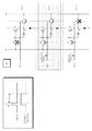
図2は、本実施形態に係る有機発光表示パネル110のサブピクセル構造の例示図である。
FIG. 2 is an exemplary diagram of the subpixel structure of the organic light emitting
図2を参照すると、本実施形態に係る有機発光表示装置100において、各サブピクセルは、有機発光ダイオード(OLED:Organic Light Emitting Diode)と、有機発光ダイオードOLEDを駆動する駆動トランジスタ(DRT:Driving Transistor)と、駆動トランジスタDRTのゲートノードに該当する第1ノードN1にデータ電圧を伝達するためのスイッチングトランジスタ(SWT:Switching Transistor)と、駆動トランジスタDRTの第2ノードN2と基準電圧(Vref:Reference Voltage)を供給する基準電圧ライン(RVL:Reference Voltage Line)との間に電気的に連結されるセンシングトランジスタ(SENT:Sensing Transistor)と、映像信号電圧に該当するデータ電圧またはこれに対応する電圧を1フレーム時間の間維持するストレージキャパシタ(Cstg:Storage Capacitor)を含んで構成できる。
Referring to FIG. 2, in the organic light emitting
有機発光ダイオードOLEDは、第1電極(例:アノード電極)、有機層及び第2電極(例:カソード電極)などからなることができる。 The organic light emitting diode OLED can be composed of a first electrode (eg, an anode electrode), an organic layer, a second electrode (eg, a cathode electrode), and the like.
駆動トランジスタDRTは、有機発光ダイオードOLEDに駆動電流を供給することによって、有機発光ダイオードOLEDを駆動する。 The drive transistor DRT drives the organic light emitting diode OLED by supplying a drive current to the organic light emitting diode OLED.
このような駆動トランジスタDRTにおいて、第1ノードN1は、スイッチングトランジスタSWTのソースノードまたはドレインノードと電気的に連結されることができ、ゲートノードでありうる。第2ノードN2は、有機発光ダイオードOLEDの第1電極と電気的に連結されることができ、ソースノードまたはドレインノードでありうる。第3ノードN3は、駆動電圧(EVDD)を供給する駆動電圧ライン(DVL:Driving Voltage Line)と電気的に連結されることができ、ドレインノードまたはソースノードでありうる。 In such a drive transistor DRT, the first node N1 can be electrically connected to the source node or drain node of the switching transistor SWT and can be a gate node. The second node N2 can be electrically connected to the first electrode of the organic light emitting diode OLED and can be a source node or a drain node. The third node N3 can be electrically connected to a driving voltage line (DVL) that supplies a driving voltage (E VDD) and can be a drain node or a source node.
スイッチングトランジスタSWTは、データラインDLと駆動トランジスタDRTの第1ノードN1との間に電気的に連結され、スキャン信号(SCAN)をゲートノードに印加を受けて制御できる。 The switching transistor SWT is electrically connected between the data line DL and the first node N1 of the drive transistor DRT, and a scan signal (SCAN) can be applied to the gate node to control it.
このようなスイッチングトランジスタSWTは、スキャン信号(SCAN)によりターン−オンされてデータラインDLから供給されたデータ電圧(Vdata)を駆動トランジスタDRTの第1ノードN1に伝達することができる。 Such a switching transistor SWT can transmit the data voltage (Vdata) that is turned on by the scan signal (SCAN) and supplied from the data line DL to the first node N1 of the drive transistor DRT.
センシングトランジスタSENTは、駆動トランジスタDRTの第2ノードN2と基準電圧ラインRVLとの間に電気的に連結され、ゲートノードにスキャン信号の一種であるセンシング信号(SENSE)の印加を受けて制御できる。 The sensing transistor SENT is electrically connected between the second node N2 of the drive transistor DRT and the reference voltage line RVL, and can be controlled by applying a sensing signal (SENSE), which is a kind of scan signal, to the gate node.
このようなセンシングトランジスタSENTはセンシング信号(SENSE)によりターン−オンされ、基準電圧ラインRVLを通じて供給される基準電圧(Vref)を駆動トランジスタDRTの第2ノードN2に印加するか、または駆動トランジスタDRTの第2ノードN2の電圧を基準電圧ラインRVLに伝達することができる。 Such a sensing transistor SENT is turned on by a sensing signal (SENSE) and applies a reference voltage (Vref) supplied through the reference voltage line RVL to the second node N2 of the drive transistor DRT, or the drive transistor DRT. The voltage of the second node N2 can be transmitted to the reference voltage line RVL.
ストレージキャパシタCstgは、駆動トランジスタDRTの第2ノードN2と第1ノードN1との間に電気的に連結できる。 The storage capacitor Cstg can be electrically connected between the second node N2 and the first node N1 of the drive transistor DRT.
このようなストレージキャパシタCstgは、駆動トランジスタDRTの第2ノードN2と第1ノードN1との間に存在する内部キャパシタ(Internal Capacitor)である寄生キャパシタ(例:Cgs、Cgd)でなく、駆動トランジスタDRTの外部に意図的に設計した外部キャパシタ(External Capacitor)である。 Such a storage capacitor Cstg is not a parasitic capacitor (eg, Cgs, Cgd) which is an internal capacitor (Internal Capacitor) existing between the second node N2 and the first node N1 of the drive transistor DRT, but the drive transistor DRT. It is an external capacitor (External Capacitor) intentionally designed outside.
駆動トランジスタDRT、スイッチングトランジスタSWT、及びセンシングトランジスタSENTは、nタイプで具現されることも、pタイプでも具現されることもできる。 The drive transistor DRT, the switching transistor SWT, and the sensing transistor SENT can be embodied in the n type or the p type.
図3は、本実施形態に係る有機発光表示パネル110のサブピクセルの1スキャン構造と2スキャン構造を示す図である。
FIG. 3 is a diagram showing a 1-scan structure and a 2-scan structure of subpixels of the organic light emitting
図3を参照すると、スイッチングトランジスタSWTのゲートノード及びセンシングトランジスタSENTのゲートノードは互いに異なるゲートラインGL1、GL2に連結できる。このようなゲートライン構造を“2スキャン構造”という。 Referring to FIG. 3, the gate node of the switching transistor SWT and the gate node of the sensing transistor SENT can be connected to different gate lines GL1 and GL2. Such a gate line structure is called a "two-scan structure".
2スキャン構造で、スイッチングトランジスタSWTのゲートノードに印加されるスキャン信号(SCAN)と、センシングトランジスタSENTのゲートノードに印加されるセンシング信号(SENSE)は別個のゲート信号でありうる。 In the two-scan structure, the scan signal (SCAN) applied to the gate node of the switching transistor SWT and the sensing signal (SENSE) applied to the gate node of the sensing transistor SENT can be separate gate signals.
したがって、スイッチングトランジスタSWTとセンシングトランジスタSENTに対する個別的なオン−オフ制御が可能である。 Therefore, individual on-off control of the switching transistor SWT and the sensing transistor SENT is possible.
図3を参照すると、スイッチングトランジスタSWTのゲートノード及びセンシングトランジスタSENTのゲートノードは、同一なゲートラインGLに連結できる。このようなゲートライン構造を“1スキャン構造”という。 Referring to FIG. 3, the gate node of the switching transistor SWT and the gate node of the sensing transistor SENT can be connected to the same gate line GL. Such a gate line structure is called a "1 scan structure".
1スキャン構造で、スイッチングトランジスタSWTのゲートノードに印加されるスキャン信号(SCAN)と、センシングトランジスタSENTのゲートノードに印加されるセンシング信号(SENSE)は同一なゲート信号でありうる。 In the one-scan structure, the scan signal (SCAN) applied to the gate node of the switching transistor SWT and the sensing signal (SENSE) applied to the gate node of the sensing transistor SENT can be the same gate signal.
したがって、スイッチングトランジスタSWTとセンシングトランジスタSENTに対する個別的なオン−オフ制御が不可能である。 Therefore, individual on-off control of the switching transistor SWT and the sensing transistor SENT is not possible.
前述した2スキャン構造はスイッチングトランジスタSWTとセンシングトランジスタSENTに対する個別的なオン−オフ制御が可能であるが、開口率が落ちる短所がある。 The two-scan structure described above allows individual on-off control of the switching transistor SWT and the sensing transistor SENT, but has the disadvantage of reducing the aperture ratio.
代わりに、1スキャン構造はスイッチングトランジスタSWTとセンシングトランジスタSENTに対する個別的なオン−オフ制御が不可能であるが、開口率が高まる長所がある。 Instead, the one-scan structure does not allow individual on-off control of the switching transistor SWT and sensing transistor SENT, but has the advantage of increasing the aperture ratio.
一方、本実施形態に係る有機発光表示装置100の場合、各サブピクセルSPの駆動時間が長くなるにつれて、有機発光ダイオードOLED、駆動トランジスタDRTなどの回路素子に対する劣化(Degradation)が進行することがある。
On the other hand, in the case of the organic light emitting
これによって、有機発光ダイオードOLED、駆動トランジスタDRTなどの回路素子が有する固有の特性値(例:しきい電圧、移動度など)が変わることがある。 As a result, the unique characteristic values (eg, threshold voltage, mobility, etc.) of circuit elements such as the organic light emitting diode OLED and the drive transistor DRT may change.
このような回路素子の特性値の変化は該当サブピクセルの輝度変化を引き起こす。 Such a change in the characteristic value of the circuit element causes a change in the brightness of the corresponding subpixel.
また、このような回路素子間の特性値の変化の程度は、各回路素子の劣化度合いの差によって互いに異なることがある。 Further, the degree of change in the characteristic value between such circuit elements may differ from each other due to the difference in the degree of deterioration of each circuit element.
このような回路素子間の特性値の変化の程度の差による回路素子間の特性値の偏差はサブピクセル間の輝度偏差を引き起こして、サブピクセルの輝度表現力に対する正確度を落とすか、または輝度不均一などの画面異常現象を起こすなどの問題を発生させることがある。 The deviation of the characteristic value between the circuit elements due to the difference in the degree of change of the characteristic value between the circuit elements causes the brightness deviation between the subpixels, which reduces the accuracy of the brightness expressiveness of the subpixels or reduces the brightness. It may cause problems such as uneven screen abnormalities.
ここで、回路素子の特性値(以下、“サブピクセル特性値”ともいう)は、一例に、駆動トランジスタDRTのしきい電圧及び移動度などを含むことができ、場合によって、有機発光ダイオードOLEDのしきい電圧を含むこともできる。 Here, the characteristic value of the circuit element (hereinafter, also referred to as “subpixel characteristic value”) can include, for example, the threshold voltage and mobility of the drive transistor DRT, and in some cases, the organic light emitting diode OLED. It can also include a threshold voltage.
本実施形態に係る有機発光表示装置100は、回路素子の特性値またはその変化をセンシング(測定)するセンシング機能と、センシング結果を用いてサブピクセル回路素子間の特性値の偏差を補償してやる補償機能を提供することができる。
The organic light emitting
図4は、本実施形態に係る有機発光表示装置100の補償回路の例示図である。
FIG. 4 is an example diagram of a compensation circuit of the organic light emitting
図4を参照すると、本実施形態に係る有機発光表示装置100は、回路素子の特性値(駆動トランジスタの特性値、有機発光ダイオードの特性値)、またはその変化をセンシングしてセンシングデータを出力するセンシング部410と、センシングデータを格納するメモリ420と、センシングデータを用いて回路素子間の特性値の偏差を補償してやる補償プロセスを遂行する補償部430などを含むことができる。
Referring to FIG. 4, the organic light emitting
センシング部410は、少なくとも1つのアナログデジタルコンバータ(ADC:Analog to Digital Converter)を含んで具現できる。 The sensing unit 410 can be embodied including at least one analog-to-digital converter (ADC).
各アナログデジタルコンバータ(ADC:Analog to Digital Converter)は、ソースドライバ集積回路SDICの内部に含まれることができ、場合によっては、ソースドライバ集積回路SDICの外部に含まれることもできる。 Each analog-to-digital converter (ADC) can be included inside the source driver integrated circuit SDIC, and in some cases, can be included outside the source driver integrated circuit SDIC.
補償部430はコントローラ140の内部に含まれることができ、場合によっては、コントローラ140の外部に含まれることもできる。
The
本実施形態に係る有機発光表示装置100は、センシング駆動を制御するために、即ち、サブピクセルSP内の駆動トランジスタDRTの第2ノードN2の電圧印加状態をサブピクセル特性値のセンシングに必要な状態に制御するために、初期化スイッチSPREとサンプリングスイッチSAMをさらに含むことができる。
The organic light emitting
初期化スイッチSPREを通じて、基準電圧ラインRVLへの基準電圧(Vref)の供給如何が制御できる。 The supply of the reference voltage (Vref) to the reference voltage line RVL can be controlled through the initialization switch SPRE.
初期化スイッチSPREがターン−オンされれば、基準電圧(Vref)が基準電圧ラインRVLに供給され、ターン−オンされているセンシングトランジスタSENTを通じて駆動トランジスタDRTの第2ノードN2に印加できる。 When the initialization switch SPRE is turned on, a reference voltage (Vref) is supplied to the reference voltage line RVL and can be applied to the second node N2 of the drive transistor DRT through the turned-on sensing transistor SENT.
一方、駆動トランジスタDRTの第2ノードN2の電圧が回路素子の特性値またはその変化を反映する電圧状態になれば、駆動トランジスタDRTの第2ノードN2と等電位でありうる基準電圧ラインRVLの電圧も回路素子の特性値またはその変化を反映する電圧状態になることができる。この際、基準電圧ラインRVL上に形成されたラインキャパシタに回路素子の特性値またはその変化を反映する電圧が充電できる。 On the other hand, if the voltage of the second node N2 of the drive transistor DRT becomes a voltage state that reflects the characteristic value of the circuit element or its change, the voltage of the reference voltage line RVL that can be equal to the second node N2 of the drive transistor DRT. Can also be in a voltage state that reflects the characteristic values of the circuit elements or their changes. At this time, the line capacitor formed on the reference voltage line RVL can be charged with a voltage that reflects the characteristic value of the circuit element or its change.
駆動トランジスタDRTの第2ノードN2の電圧が回路素子の特性値またはその変化を反映する電圧状態になれば、サンプリングスイッチSAMがターン−オンされて、センシング部410と基準電圧ラインRVLとが連結できる。 When the voltage of the second node N2 of the drive transistor DRT becomes a voltage state that reflects the characteristic value of the circuit element or its change, the sampling switch SAM is turned on and the sensing unit 410 and the reference voltage line RVL can be connected. ..
これによって、センシング部410は回路素子の特性値またはその変化を反映する電圧状態である基準電圧ラインRVLの電圧(即ち、駆動トランジスタDRTの第2ノードN2の電圧)をセンシングする。 As a result, the sensing unit 410 senses the voltage of the reference voltage line RVL (that is, the voltage of the second node N2 of the drive transistor DRT), which is a voltage state that reflects the characteristic value of the circuit element or its change.
センシング部410は、センシングされた電圧をデジタル値に該当するセンシング値に変換し、センシング値を含むセンシングデータを転送する。 The sensing unit 410 converts the sensed voltage into a sensing value corresponding to a digital value, and transfers the sensing data including the sensing value.
センシング部410により転送されたセンシングデータはメモリ420に格納される。 The sensing data transferred by the sensing unit 410 is stored in the memory 420.
補償部430は、メモリ420に格納されたセンシングデータを用いて各回路素子間の偏差を補償するための補償プロセスを遂行することができる。
The
以下では、駆動トランジスタDRTに対するしきい電圧センシング駆動及び移動度センシング駆動について簡略に説明する。 In the following, the threshold voltage sensing drive and the mobility sensing drive for the drive transistor DRT will be briefly described.
図5は、本実施形態に係る有機発光表示装置100の駆動トランジスタDRTに対するしきい電圧センシング駆動方式を説明するための図である。
FIG. 5 is a diagram for explaining a threshold voltage sensing drive method for the drive transistor DRT of the organic light
駆動トランジスタDRTに対するしきい電圧センシング駆動時、駆動トランジスタDRTの第1ノードN1と第2ノードN2の各々は、しきい電圧センシング駆動用データ電圧(Vdata)と基準電圧(Vref)に初期化される。 When driving the threshold voltage sensing for the drive transistor DRT, each of the first node N1 and the second node N2 of the drive transistor DRT is initialized to the threshold voltage sensing drive data voltage (Vdata) and the reference voltage (Vref). ..
以後、初期化スイッチSPREがオフされて駆動トランジスタDRTの第2ノードN2がフローティング(Floating)される。 After that, the initialization switch SPRE is turned off and the second node N2 of the drive transistor DRT is floated.
これによって、駆動トランジスタDRTの第2ノードN2の電圧が上昇する。 As a result, the voltage of the second node N2 of the drive transistor DRT rises.
駆動トランジスタDRTの第2ノードN2の電圧は上昇がなされてから上昇幅が徐々に減って飽和するようになる。 After the voltage of the second node N2 of the drive transistor DRT is increased, the increase width gradually decreases and becomes saturated.
駆動トランジスタDRTの第2ノードN2の飽和された電圧は、データ電圧(Vdata)としきい電圧(Vth)の差、またはデータ電圧(Vdata)としきい電圧偏差(ΔVth)の差に該当できる。 The saturated voltage of the second node N2 of the drive transistor DRT can correspond to the difference between the data voltage (Vdata) and the threshold voltage (Vth), or the difference between the data voltage (Vdata) and the threshold voltage deviation (ΔVth).
センシング部410は駆動トランジスタDRTの第2ノードN2の電圧が飽和されれば、駆動トランジスタDRTの第2ノードN2の飽和された電圧をセンシングする。 If the voltage of the second node N2 of the drive transistor DRT is saturated, the sensing unit 410 senses the saturated voltage of the second node N2 of the drive transistor DRT.
センシング部410によりセンシングされた電圧(Vsen)は、データ電圧(Vdata)からしきい電圧(Vth)を引いた電圧(Vdata−Vth)、またはデータ電圧(Vdata)からしきい電圧偏差(ΔVth)を引いた電圧(Vdata−ΔVth)でありうる。 The voltage (Vsen) sensed by the sensing unit 410 is the voltage (Vdata-Vth) obtained by subtracting the threshold voltage (Vth) from the data voltage (Vdata), or the threshold voltage deviation (ΔVth) from the data voltage (Vdata). It can be the subtracted voltage (Vdata-ΔVth).
図6は、本実施形態に係る有機発光表示装置100の駆動トランジスタDRTに対する移動度センシング駆動方式を説明するための図である。
FIG. 6 is a diagram for explaining a mobility sensing drive method for the drive transistor DRT of the organic light emitting
移動度センシング駆動時、駆動トランジスタDRTの第1ノードN1と第2ノードN2の各々は移動度センシング駆動用データ電圧(Vdata)と基準電圧(Vref)に初期化される。 During the mobility sensing drive, each of the first node N1 and the second node N2 of the drive transistor DRT is initialized to the mobility sensing drive data voltage (Vdata) and the reference voltage (Vref).
以後、スイッチングトランジスタSWTがターン−オフされ、初期化スイッチSPREがオフされて、駆動トランジスタDRTの第1ノードN1と第2ノードN2がフローティングされる。 After that, the switching transistor SWT is turned off, the initialization switch SPRE is turned off, and the first node N1 and the second node N2 of the drive transistor DRT are floated.
これによって、駆動トランジスタDRTの第2ノードN2の電圧が上昇し始める。 As a result, the voltage of the second node N2 of the drive transistor DRT begins to rise.
駆動トランジスタDRTの第2ノードN2の電圧上昇速度(時間に対する電圧上昇値の変化量(ΔV))は、駆動トランジスタDRTの電流能力、即ち移動度によって変わる。 The voltage rise rate (change amount (ΔV) of the voltage rise value with time) of the second node N2 of the drive transistor DRT changes depending on the current capacity of the drive transistor DRT, that is, the mobility.
即ち、電流能力(移動度)が大きい駆動トランジスタDRTであるほど、駆動トランジスタDRTの第2ノードN2の電圧がさらに急激に上昇する。 That is, the larger the current capacity (mobility) of the drive transistor DRT, the more rapidly the voltage of the second node N2 of the drive transistor DRT rises.
駆動トランジスタDRTの第2ノードN2の電圧が予め定まった一定時間の間上昇がなされた以後、センシング部410は駆動トランジスタDRTの第2ノードN2の上昇された電圧(即ち、駆動トランジスタDRTの第2ノードN2の電圧上昇によって共に電圧上昇がなされた基準電圧ラインRVLの電圧)をセンシングする。 After the voltage of the second node N2 of the drive transistor DRT is increased for a predetermined fixed time, the sensing unit 410 uses the increased voltage of the second node N2 of the drive transistor DRT (that is, the second of the drive transistor DRT). The voltage of the reference voltage line RVL in which the voltage is raised by the voltage rise of the node N2) is sensed.
前述したしきい電圧または移動度センシング駆動によってセンシング部410はしきい電圧センシングまたは移動度センシングのためにセンシングされた電圧(Vsen)をデジタル値に変換し、変換されたデジタル値(センシング値)を含むセンシングデータを生成して出力する。 The sensing unit 410 converts the voltage (Vsen) sensed for the threshold voltage sensing or mobility sensing into a digital value by the above-mentioned threshold voltage or mobility sensing drive, and converts the converted digital value (sensing value) into a digital value. Generates and outputs the including sensing data.
センシング部410で出力されたセンシングデータは、メモリ420に格納されるか、または補償部430に提供できる。
The sensing data output by the sensing unit 410 can be stored in the memory 420 or provided to the
補償部430はメモリ420に格納されるか、またはセンシング部410で提供されたセンシングデータに基づいて該当サブピクセル内の駆動トランジスタDRTの特性値(例:しきい電圧、移動度)、または駆動トランジスタDRTの特性値の変化(例:しきい電圧変化、移動度の変化)を把握し、特性値補償プロセスを遂行することができる。
The
ここで、駆動トランジスタDRTの特性値の変化は以前センシングデータを基準に現在センシングデータが変化されたことを意味するか、または基準センシングデータを基準に現在センシングデータが変化されたことを意味することもできる。 Here, the change in the characteristic value of the drive transistor DRT means that the current sensing data has been changed based on the previously sensing data, or that the current sensing data has been changed based on the reference sensing data. You can also.
ここで、駆動トランジスタDRT間の特性値または特性値の変化を比較して見ると、駆動トランジスタDRT間の特性値の偏差を把握することができる。駆動トランジスタDRTの特性値の変化が基準センシングデータを基準に現在センシングデータが変化されたことを意味する場合、駆動トランジスタDRTの特性値の変化から駆動トランジスタDRT間の特性値の偏差(即ち、サブピクセル輝度偏差)を把握することもできる。 Here, by comparing the characteristic value or the change in the characteristic value between the drive transistor DRTs, the deviation of the characteristic value between the drive transistor DRTs can be grasped. If the change in the characteristic value of the drive transistor DRT means that the current sensing data has changed with respect to the reference sensing data, the deviation of the characteristic value between the drive transistor DRT from the change in the characteristic value of the drive transistor DRT (that is, the sub). It is also possible to grasp the pixel brightness deviation).
特性値補償プロセスは、駆動トランジスタDRTのしきい電圧を補償するしきい電圧補償処理と、駆動トランジスタDRTの移動度を補償する移動度補償処理を含むこともできる。 The characteristic value compensation process can also include a threshold voltage compensation process for compensating for the threshold voltage of the drive transistor DRT and a mobility compensation process for compensating for the mobility of the drive transistor DRT.
しきい電圧補償処理は、しきい電圧またはしきい電圧偏差(しきい電圧の変化)を補償するための補償値を演算し、演算された補償値をメモリ420に格納するか、または演算された補償値に該当映像データ(Data)を変更する処理を含むことができる。 The threshold voltage compensation process calculates a compensation value for compensating for the threshold voltage or the threshold voltage deviation (change in the threshold voltage), and stores the calculated compensation value in the memory 420 or is calculated. The compensation value can include a process of changing the corresponding video data (Data).
移動度補償処理は移動度または移動度の偏差(移動度の変化)を補償するための補償値を演算し、演算された補償値をメモリ420に格納するか、または演算された補償値に該当映像データ(Data)を変更する処理を含むことができる。 The mobility compensation process calculates a compensation value for compensating for mobility or mobility deviation (change in mobility), and stores the calculated compensation value in the memory 420, or corresponds to the calculated compensation value. It can include a process of changing the video data (Data).
補償部430はしきい電圧補償処理または移動度補償処理により映像データ(Data)を変更して、変更されたデータをデータドライバ120内の該当ソースドライバ集積回路SDICに供給することができる。
The
これによって、該当ソースドライバ集積回路SDICは、補償部430で変更されたデータをデジタルアナログコンバータ(DAC:Digital to Analog Converter)を通じてデータ電圧に変換して該当サブピクセルに供給することによって、サブピクセル特性値補償(しきい電圧補償、移動度補償)が実際になされるようになる。
As a result, the corresponding source driver integrated circuit SDIC converts the data changed by the
このようなサブピクセル特性値補償がなされるにつれて、サブピクセル間の輝度偏差を減らすか、または防止することによって、画像品質を向上させることができる。 As such subpixel characteristic value compensation is performed, the image quality can be improved by reducing or preventing the luminance deviation between the subpixels.
図7は、本実施形態に係る有機発光表示装置100の有機発光ダイオードOLEDの劣化センシング駆動方式を説明するための図である。
FIG. 7 is a diagram for explaining a deterioration sensing drive method of the organic light emitting diode OLED of the organic light emitting
図7を参照すると、有機発光ダイオードOLEDの劣化をセンシングする駆動は、駆動トランジスタDRTの第1ノードN1と第2ノードN2を初期化する初期化ステップ(S710)、有機発光ダイオードOLEDの劣化をトラッキングするOLED劣化トラッキングステップ(S720)、及び有機発光ダイオードOLEDの劣化度合いを示す電圧をセンシングするOLED劣化センシングステップ(S730)に進行できる。 Referring to FIG. 7, the drive for sensing the deterioration of the organic light emitting diode OLED is the initialization step (S710) for initializing the first node N1 and the second node N2 of the drive transistor DRT, and tracking the deterioration of the organic light emitting diode OLED. It is possible to proceed to the OLED deterioration tracking step (S720) and the OLED deterioration sensing step (S730) for sensing a voltage indicating the degree of deterioration of the organic light emitting diode OLED.
初期化ステップ(S710)で、スイッチングトランジスタSWT及びセンシングトランジスタSENTを全てターン−オンさせて、駆動トランジスタDRTの第1ノードN1と第2ノードN2を有機発光ダイオードOLEDの劣化センシング用データ電圧(Vdata)と基準電圧(Vref)に初期化させる。 In the initialization step (S710), the switching transistor SWT and the sensing transistor SENT are all turned on, and the first node N1 and the second node N2 of the drive transistor DRT are set to the deterioration sensing data voltage (Vdata) of the organic light emitting diode OLED. And the reference voltage (Vref).
OLED劣化トラッキングステップ(S720)では、センシングトランジスタSENTのみをターン−オフさせて、駆動トランジスタDRTの第2ノードN2をフローティングさせて、駆動トランジスタDRTの第2ノードN2の電圧を変化させる。 In the OLED deterioration tracking step (S720), only the sensing transistor SENT is turned off, the second node N2 of the drive transistor DRT is floated, and the voltage of the second node N2 of the drive transistor DRT is changed.
OLED劣化トラッキングステップ(S720)で、駆動トランジスタDRTの第2ノードN2の電圧が上昇してから、有機発光ダイオードOLEDが発光する。 In the OLED deterioration tracking step (S720), the voltage of the second node N2 of the drive transistor DRT rises, and then the organic light emitting diode OLED emits light.
有機発光ダイオードOLEDが発光する時の駆動トランジスタDRTの第2ノードN2の電圧は、有機発光ダイオードOLEDの劣化度合いによって変わる。 The voltage of the second node N2 of the drive transistor DRT when the organic light emitting diode OLED emits light changes depending on the degree of deterioration of the organic light emitting diode OLED.
したがって、OLED劣化センシングステップ(S730)では、スイッチングトランジスタSWTはターン−オフさせ、センシングトランジスタSENTはターン−オンさせて、アナログデジタルコンバータADCでありうるセンシング部410を通じて、駆動トランジスタDRTの第2ノードN2の電圧を検出して、有機発光ダイオードOLEDの劣化度合いをセンシングすることができる。 Therefore, in the OLED deterioration sensing step (S730), the switching transistor SWT is turned off and the sensing transistor SENT is turned on, and the second node N2 of the drive transistor DRT is passed through the sensing unit 410 which can be an analog-to-digital converter ADC. The voltage of the organic light emitting diode OLED can be detected to sense the degree of deterioration of the organic light emitting diode OLED.
前述したように、本実施形態に係る有機発光表示装置100は、一般的な映像を表示するための映像駆動モードと、駆動トランジスタDRTのしきい電圧をセンシングして補償してやる駆動トランジスタしきい電圧補償モードと、駆動トランジスタDRTの移動度をセンシングして補償してやる駆動トランジスタ移動度補償モードと、有機発光ダイオードOLEDの劣化(しきい電圧)をセンシングして補償してやる残像補償モードなどを提供することができる。
As described above, the organic light emitting
映像駆動モード、駆動トランジスタしきい電圧補償モード、及び駆動トランジスタ移動度補償モードは、サブピクセルが1スキャン構造の場合と2スキャン構造の場合に全て可能である。 The video drive mode, the drive transistor threshold voltage compensation mode, and the drive transistor mobility compensation mode are all possible when the subpixel has a 1-scan structure and a 2-scan structure.
しかしながら、残像補償モードは、スイッチングトランジスタSWT及びセンシングトランジスタSENTの各々のオン−オフが別途に制御されなければならないので、1スキャン構造でも適用し難く、2スキャン構造のみで適用することができる。 However, since the on-off of each of the switching transistor SWT and the sensing transistor SENT must be controlled separately, the afterimage compensation mode is difficult to apply even with a one-scan structure, and can be applied only with a two-scan structure.
しかしながら、2スキャン構造でサブピクセルを設計する場合、開口率の減少が不回避である。 However, when designing subpixels with a two-scan structure, a reduction in aperture ratio is unavoidable.
ここに、以下の本実施形態は、残像補償モードに適用できる1スキャン構造を開示する。 Here, the following embodiment discloses a one-scan structure applicable to the afterimage compensation mode.
図8及び図9は、本実施形態に係る有機発光表示パネル110の改善構造である。
8 and 9 are improved structures of the organic light emitting
前述したように、各サブピクセルは、有機発光ダイオードOLEDと、有機発光ダイオードOLEDを駆動するための駆動トランジスタDRTと、ゲートノードに印加されるスキャン信号(SCAN)により制御され、駆動トランジスタDRTの第1ノードN1とデータラインDLとの間に電気的に連結されたスイッチングトランジスタSWTと、ゲートノードに印加されるセンシング信号(SENSE)により制御され、駆動トランジスタDRTと第2ノードN2と基準電圧ラインRVLとの間に電気的に連結されたセンシングトランジスタSENTと、駆動トランジスタDRTの第1ノードN1と第2ノードN2との間に電気的に連結されたストレージキャパシタCstgとを含む。 As described above, each subpixel is controlled by the organic light emitting diode OLED, the drive transistor DRT for driving the organic light emitting diode OLED, and the scan signal (SCAN) applied to the gate node, and is the first of the drive transistor DRT. The drive transistor DRT, the second node N2, and the reference voltage line RVL are controlled by the switching transistor SWT electrically connected between the 1 node N1 and the data line DL and the sensing signal (SENSE) applied to the gate node. It includes a sensing transistor SENT electrically connected to and a storage capacitor Cstg electrically connected between the first node N1 and the second node N2 of the drive transistor DRT.
図8及び図9を参照すると、有機発光表示パネル110には複数のサブピクセルライン(・・・,SPLn−1、SPLn,SPLn+1,・・・)が配列され、複数のゲートライン(・・・,GLn−1,GLn,GLn+1,・・・)が配置される。
Referring to FIGS. 8 and 9, a plurality of sub-pixel lines (..., SPLn-1, SPLn, SPLn + 1, ...) Are arranged on the organic light emitting
図8及び図9を参照すると、複数のゲートライン(・・・,GLn−1,GLn,GLn+1,・・・)の各々は1つのサブピクセルライン毎に配置される。 With reference to FIGS. 8 and 9, each of the plurality of gate lines (..., GLn-1, GLn, GLn + 1, ...) Is arranged for each subpixel line.
図8及び図9を参照すると、複数のゲートライン(・・・,GLn−1,GLn,GLn+1,・・・)のうちのn番目サブピクセルラインSPLnに配置されたn番目ゲートラインGLnは、n番目サブピクセルラインSPLnに配列された各サブピクセルSPn内のスイッチングトランジスタSWTのゲートノードと、n−1番目サブピクセルラインSPLn−1に配列された各サブピクセルSPn−1内のセンシングトランジスタSENTのゲートノードに共通に連結できる。 With reference to FIGS. 8 and 9, the nth gate line GLn arranged at the nth subpixel line SPLn of the plurality of gate lines (..., GLn-1, GLn, GLn + 1, ...) Is The gate node of the switching transistor SWT in each subpixel SPn arranged in the nth subpixel line SPLn and the sensing transistor SENT in each subpixel SPn-1 arranged in the n-1st subpixel line SPLn-1. Can be commonly linked to gate nodes.
複数のゲートライン(・・・,GLn−1,GLn,GLn+1,・・・)のうちのn+1番目サブピクセルラインSPLn+1に配置されたn+1番目ゲートラインGLn+1は、n+1番目サブピクセルラインSPLn+1に配列された各サブピクセルSPn+1内のスイッチングトランジスタSWTのゲートノードと、n番目サブピクセルラインSPLnに配列された各サブピクセルSPn内のセンシングトランジスタSENTのゲートノードに共通に連結できる。
The n + 1th gate line GLn + 1 arranged on the n + 1st subpixel
前述したゲートライン連結構造を活用すれば、スイッチングトランジスタSWT及びセンシングトランジスタSENTの個別的なオン−オフ制御可能な1スキャン構造を作ることができる。 By utilizing the gateline connection structure described above, it is possible to create a one-scan structure in which the switching transistor SWT and the sensing transistor SENT can be individually turned on and off.
このような1スキャン構造を通じて開口率を高めながらも、スイッチングトランジスタSWT及びセンシングトランジスタSENTの個別的なオン−オフ制御が必要な各種駆動モード(例:残像補償モード)を可能にすることができる。 While increasing the aperture ratio through such a one-scan structure, it is possible to enable various drive modes (eg, afterimage compensation mode) that require individual on-off control of the switching transistor SWT and the sensing transistor SENT.
前述したゲートライン構造によれば、各サブピクセル内のスイッチングトランジスタSWT及びセンシングトランジスタSENTの各々のゲートノードは、次のような方式により印加できる。 According to the gate line structure described above, each gate node of the switching transistor SWT and the sensing transistor SENT in each subpixel can be applied by the following method.
図8及び図9を参照すると、n−1番目サブピクセルラインSPLn−1に配列された各サブピクセルSPn−1内のスイッチングトランジスタSWTのゲートノードは、n−1番目サブピクセルラインSPLn−1に配置されたn−1番目ゲートラインGLn−1を通じて出力されるn−1番目スキャン信号(SCANn−1)の印加を受ける。 Referring to FIGS. 8 and 9, the gate node of the switching transistor SWT in each subpixel SPn-1 arranged on the n-1st subpixel line SPLn-1 is located on the n-1st subpixel line SPLn-1. The n-1st scan signal (SCANn-1) output through the arranged n-1st gate line GLn-1 is applied.
n−1番目サブピクセルラインSPLn−1に配列された各サブピクセルSPn−1内のセンシングトランジスタSENTのゲートノードは、n番目サブピクセルラインSPLnに配置されたn番目ゲートラインGLnを通じて出力されるn番目スキャン信号(SCANn)をn−1番目センシング信号(SENSEn−1)として印加を受ける。 The gate node of the sensing transistor SENT in each subpixel SPn-1 arranged on the n-1st subpixel line SPLn-1 is output through the nth gateline GLn arranged on the nth subpixel line SPLn. The second scan signal (SCANn) is applied as the n-1st sensing signal (SENSEn-1).
図8及び図9を参照すると、n番目サブピクセルラインSPLnに配列された各サブピクセルSPn内のスイッチングトランジスタSWTのゲートノードは、n番目サブピクセルラインSPLnに配置されたn番目ゲートラインGLnを通じて出力されるn番目スキャン信号(SCANn)の印加を受ける。 Referring to FIGS. 8 and 9, the gate node of the switching transistor SWT in each subpixel SPn arranged on the nth subpixel line SPLn outputs through the nth gateline GLn arranged on the nth subpixel line SPLn. The nth scan signal (SCANn) is applied.
n番目サブピクセルラインSPLnに配列された各サブピクセルSPn内のセンシングトランジスタSENTのゲートノードは、n+1番目サブピクセルラインSPLn+1に配置されたn+1番目ゲートラインGLn+1を通じて出力されるn+1番目スキャン信号(SCANn+1)をn番目センシング信号(SENSEn)として印加を受ける。
The gate node of the sensing transistor SENT in each subpixel SPn arranged on the nth subpixel line SPLn is an n + 1th scan signal (SCANn + 1) output through the n + 1th gate line GLn + 1 arranged on the n + 1th subpixel
前述した方式に従って、各サブピクセル内のスイッチングトランジスタSWT及びセンシングトランジスタSENTの各々にゲート信号(SCAN、SENSE)を個別的に伝達することによって、各サブピクセルライン毎に配置された1つのゲートラインだけでも、即ち1スキャン構造だけでも、スイッチングトランジスタSWT及びセンシングトランジスタSENTのオン−オフを個別的に制御することができる。 By individually transmitting gate signals (SCAN, SENSE) to each of the switching transistor SWT and sensing transistor SENT in each subpixel according to the method described above, only one gate line arranged for each subpixel line is provided. However, that is, the on-off of the switching transistor SWT and the sensing transistor SENT can be individually controlled by using only one scan structure.
これによって、1スキャン構造を通じて開口率を高めながらも、スイッチングトランジスタSWT及びセンシングトランジスタSENTの個別的なオン−オフ制御が必要な駆動モード(例:残像補償モード)を可能にすることができる。 This makes it possible to enable a drive mode (eg, afterimage compensation mode) that requires individual on-off control of the switching transistor SWT and the sensing transistor SENT while increasing the aperture ratio through the one-scan structure.
以下、前述したゲートライン構造に従う4種類の駆動モード(映像駆動モード、残像補償モード、駆動トランジスタしきい電圧補償モード、駆動トランジスタ移動度補償モード)について説明する。 Hereinafter, four types of drive modes (video drive mode, afterimage compensation mode, drive transistor threshold voltage compensation mode, and drive transistor mobility compensation mode) according to the gate line structure described above will be described.
図10は本実施形態に係る有機発光表示パネル110の改善構造における4種類の駆動モード(映像駆動モード、残像補償モード、駆動トランジスタしきい電圧補償モード、駆動トランジスタ移動度補償モード)に従うスキャン信号タイミング図である。但し、9のスキャン信号タイミング図は、n番目サブピクセルラインSPLnを基準としたものである。
FIG. 10 shows the scan signal timing according to four types of drive modes (image drive mode, afterimage compensation mode, drive transistor threshold voltage compensation mode, drive transistor mobility compensation mode) in the improved structure of the organic light emitting
図10を参照すると、n番目サブピクセルラインSPLnに対する映像駆動モードで、n番目スキャン信号(SCANn)のターン−オンレベル電圧区間と、n+1番目スキャン信号(SCANn+1)のターン−オンレベル電圧区間とは一部重畳できる。 Referring to FIG. 10, in the video drive mode for the nth subpixel line SPLn, the turn-on level voltage section of the nth scan signal (SCANn) and the turn-on level voltage section of the n + 1th scan signal (SCANn + 1) are Partially can be superimposed.
図10を参照すると、n番目サブピクセルラインSPLnに対する残像補償モードで、n番目スキャン信号(SCANn)がターン−オンレベル電圧で出力される間、n+1番目スキャン信号(SCANn+1)がターン−オンレベル電圧で出力されてからターン−オフレベル電圧に変わって出力され、n番目スキャン信号(SCANn)がターン−オンレベル電圧からターン−オフレベル電圧に変わって出力されれば、n+1番目スキャン信号(SCANn+1)がターン−オンレベル電圧で出力できる。 Referring to FIG. 10, in the afterimage compensation mode for the nth subpixel line SPLn, the n + 1th scan signal (SCANn + 1) is the turn-on level voltage while the nth scan signal (SCANn) is output at the turn-on level voltage. If the output is changed to the turn-off level voltage and then the nth scan signal (SCANn) is changed from the turn-on level voltage to the turn-off level voltage, the n + 1th scan signal (SCANn + 1) is output. Can be output at turn-on level voltage.
図10を参照すると、n番目サブピクセルラインSPLnでの駆動トランジスタDRTのしきい電圧補償モードで、n番目スキャン信号(SCANn)のターン−オンレベル電圧区間と、n+1番目スキャン信号(SCANn+1)のターン−オンレベル電圧区間とは重畳できる。 Referring to FIG. 10, in the threshold voltage compensation mode of the drive transistor DRT at the nth subpixel line SPLn, the turn-on-level voltage interval of the nth scan signal (SCANn) and the turn of the n + 1th scan signal (SCANn + 1). -Can be superimposed on the on-level voltage section.
図10を参照すると、n番目サブピクセルラインSPLnでの駆動トランジスタDRTの移動度補償モードで、n+1番目スキャン信号(SCANn+1)がターン−オンレベル電圧で出力される間、n番目スキャン信号(SCANn)がターン−オンレベル電圧で出力されてからターン−オフレベル電圧で出力できる。 Referring to FIG. 10, in the mobility compensation mode of the drive transistor DRT at the nth subpixel line SPLn, the nth scan signal (SCANn) is output while the n + 1th scan signal (SCANn + 1) is output at the turn-on level voltage. Can be output at the turn-on level voltage and then at the turn-off level voltage.
スイッチングトランジスタSWT及びセンシングトランジスタSENTがnタイプのトランジスタの場合、ターン−オンレベル電圧はハイレベルゲート電圧(VGH)で、ターン−オフレベル電圧はローレベルゲート電圧(VGL)でありうる。 When the switching transistor SWT and the sensing transistor SENT are n-type transistors, the turn-on level voltage can be the high level gate voltage (VGH) and the turn-off level voltage can be the low level gate voltage (VGL).
スイッチングトランジスタSWT及びセンシングトランジスタSENTがpタイプのトランジスタの場合、ターン−オンレベル電圧はローレベルゲート電圧(VGL)で、ターン−オフレベル電圧はハイレベルゲート電圧(VGH)でありうる。 When the switching transistor SWT and the sensing transistor SENT are p-type transistors, the turn-on level voltage can be the low level gate voltage (VGL) and the turn-off level voltage can be the high level gate voltage (VGH).
図11から図14は、本実施形態に係る有機発光表示パネル110の改善構造下で、映像駆動モードに従うサブピクセルの駆動を説明するための図である。
11 to 14 are diagrams for explaining the driving of sub-pixels according to the video driving mode under the improved structure of the organic light emitting
図11を参照すると、映像駆動のための各スキャン信号は2H長さのターン−オンレベル電圧区間を有する。 Referring to FIG. 11, each scan signal for video drive has a turn-on level voltage interval of 2H length.
図11を参照すると、n番目サブピクセルラインSPLnに対する映像駆動モード区間は、タイミングマージン確保区間(A)と充電区間(B)からなる。 Referring to FIG. 11, the video drive mode section for the nth subpixel line SPLn includes a timing margin securing section (A) and a charging section (B).
図11及び図12を参照すると、n番目サブピクセルラインSPLnに対する映像駆動モードで、タイミングマージン確保区間(A)の間、n番目サブピクセルラインSPLに配置されたn番目ゲートラインGLnで出力されたn番目スキャン信号(SCANn)のターン−オンレベル電圧によりn番目サブピクセルラインSPLnに配列された各サブピクセルSPn内のスイッチングトランジスタSWTとセンシングトランジスタSENTのうち、スイッチングトランジスタSWTのみターン−オンされる。 With reference to FIGS. 11 and 12, in the video drive mode for the nth subpixel line SPLn, the output was made at the nth gate line GLn arranged on the nth subpixel line SPL during the timing margin securing section (A). Of the switching transistor SWT and sensing transistor SENT in each subpixel SPn arranged on the nth subpixel line SPLn by the turn-on level voltage of the nth scan signal (SCANn), only the switching transistor SWT is turned on.
これによって、映像駆動用データ電圧が駆動トランジスタDRTの第1ノードN1に印加される。 As a result, the video drive data voltage is applied to the first node N1 of the drive transistor DRT.
ここで、タイミングマージン確保区間(A)は、n番目サブピクセルラインSPLnに配列された各サブピクセルSPn内のセンシングトランジスタSENTのゲートノードに印加されるn番目センシング信号(SENSEn)がn+1番目サブピクセルラインSPLn+1に配置されたn+1番目ゲートラインGLn+1で出力されたn+1番目スキャン信号(SCANn+1)であるため、必要なタイミング区間である。
Here, in the timing margin securing section (A), the nth sensing signal (SENSEN) applied to the gate node of the sensing transistor SENT in each subpixel SPn arranged on the nth subpixel line SPLn is the n + 1th subpixel. Since it is the n + 1st scan signal (SCANn + 1) output by the n + 1st gate line GLn + 1 arranged on the
図11及び図13を参照すると、充電区間(B)の間、n番目センシング信号(SENSEn)の役割をするn+1番目スキャン信号(SCANn+1)のターン−オンレベル電圧によりn番目サブピクセルラインSPLnに配列された各サブピクセルSPn内のセンシングトランジスタSENTもさらにターン−オンされる。 With reference to FIGS. 11 and 13, during the charging section (B), the n + 1th scan signal (SCANn + 1) acting as the nth sensing signal (SENSEN) is arranged on the nth subpixel line SPLn by the turn-on level voltage. The sensing transistor SENT in each subpixel SPn is also turned on.
これによって、駆動トランジスタDRTの第1ノードN1と第2ノードN2には映像駆動用データ電圧と基準電圧が印加されて、駆動トランジスタDRTの第1ノードN1と第2ノードN2の電位差に該当する電圧がストレージキャパシタCstgに充電される。 As a result, the video drive data voltage and the reference voltage are applied to the first node N1 and the second node N2 of the drive transistor DRT, and the voltage corresponding to the potential difference between the first node N1 and the second node N2 of the drive transistor DRT. Is charged into the storage capacitor Cstg.
以後、n番目スキャン信号(SCANn)のターン−オフレベル電圧によりn番目サブピクセルラインSPLnに配列された各サブピクセルSPn内のスイッチングトランジスタSWTがターン−オフされ、n番目センシング信号(SENSEn)の役割をするn+1番目スキャン信号(SCANn+1)のターン−オフレベル電圧によりn番目サブピクセルラインSPLnに配列された各サブピクセルSPn内のセンシングトランジスタSENTがターン−オフされることによって、駆動トランジスタDRTの第1ノードN1と第2ノードN2が全てフローティングされれば、駆動トランジスタDRTの第2ノードN2の電圧が上昇しながら有機発光ダイオードOLEDに電流が供給されて、有機発光ダイオードOLEDが発光する。 After that, the turn-off level voltage of the nth scan signal (SCANn) turns off the switching transistor SWT in each subpixel SPn arranged on the nth subpixel line SPLn, and the role of the nth sensing signal (SENSEN) is changed. The first of the drive transistors DRT is turned off by the turn-off level voltage of the n + 1th scan signal (SCANn + 1) that turns off the sensing transistor SENT in each subpixel SPn arranged on the nth subpixel line SPLn. If the node N1 and the second node N2 are all floated, a current is supplied to the organic light emitting diode OLED while the voltage of the second node N2 of the drive transistor DRT rises, and the organic light emitting diode OLED emits light.
一方、図11及び図14を参照すると、n番目サブピクセルラインSPLnに対する映像駆動モードで、充電区間(B)の以後、A’区間では、n番目ゲートラインGLnで出力されたn番目スキャン信号(SCANn)のターン−オフレベル電圧によりn番目サブピクセルラインSPLnに配列された各サブピクセルSPn内のスイッチングトランジスタSWTをターン−オフさせる。A’区間でn番目サブピクセルラインSPLnに配列された各サブピクセルSPn内のセンシングトランジスタSENTはターン−オン状態に維持される。このようなA’区間はn+1番目サブピクセルラインSPLn+1に対する映像駆動モードのためのタイミングマージン確保区間に該当することができる。
On the other hand, referring to FIGS. 11 and 14, in the video drive mode for the nth subpixel line SPLn, after the charging section (B), in the A'section, the nth scan signal output at the nth gate line GLn ( The turn-off level voltage of SCANn) turns off the switching transistor SWT in each subpixel SPn arranged on the nth subpixel line SPLn. The sensing transistor SENT in each subpixel SPn arranged on the nth subpixel line SPLn in the A'interval is maintained in the turn-on state. Such an A'section can correspond to a timing margin securing section for the video drive mode for the n + 1th subpixel
前述したように、n番目サブピクセルラインSPLnに対する映像駆動モードで、n番目スキャン信号(SCANn)のターン−オンレベル電圧区間と、n+1番目スキャン信号(SCANn+1)のターン−オンレベル電圧区間とは一部重畳できる。 As described above, in the video drive mode for the nth subpixel line SPLn, the turn-on level voltage section of the nth scan signal (SCANn) and the turn-on level voltage section of the n + 1th scan signal (SCANn + 1) are one. Can be superimposed.
即ち、n番目サブピクセルラインSPLnに対する映像駆動モードで、n番目スキャン信号(SCANn)のターン−オンレベル電圧区間の後半部区間が、n+1番目スキャン信号(SCANn+1)のターン−オンレベル電圧区間の前半部区間と重畳できる。 That is, in the video drive mode for the nth subpixel line SPLn, the latter half of the turn-on level voltage section of the nth scan signal (SCANn) is the first half of the turn-on level voltage section of the n + 1th scan signal (SCANn + 1). Can be superimposed on a section.
これを通じて、n+1番目サブピクセルラインSPLn+1に配置されたn+1番目ゲートラインGLn+1で出力されたn+1番目スキャン信号(SCANn+1)をn番目サブピクセルラインSPLnに配列された各サブピクセルSPn内のセンシングトランジスタSENTのゲートノードに印加されるn番目センシング信号(SENSEn)に活用しても、正常な映像駆動を可能にすることができる。
Through this, the n + 1th scan signal (SCANn + 1) output by the n + 1th gate line GLn + 1 arranged on the n + 1th subpixel
図15から図17は、本実施形態に係る有機発光表示パネル110の改善構造下で、残像補償モード(OLED劣化センシングを通じてのOLED劣化補償モード)に従うサブピクセルの駆動を説明するための図である。
15 to 17 are diagrams for explaining the driving of subpixels according to the afterimage compensation mode (OLED deterioration compensation mode through OLED deterioration sensing) under the improved structure of the organic light emitting
図15から図17を参照すると、残像補償モードは、駆動トランジスタDRTの第1ノードN1と第2ノードN2を初期化する初期化ステップ(D)、有機発光ダイオードOLEDの劣化をトラッキングするOLED劣化トラッキングステップ(E)と、有機発光ダイオードOLEDの劣化度合いを示した電圧をセンシングするOLED劣化センシングステップ(F)に進行できる。 Referring to FIGS. 15 to 17, the afterimage compensation mode is an initialization step (D) for initializing the first node N1 and the second node N2 of the drive transistor DRT, and OLED deterioration tracking for tracking the deterioration of the organic light emitting diode OLED. The process can proceed to step (E) and an OLED deterioration sensing step (F) that senses a voltage indicating the degree of deterioration of the organic light emitting diode OLED.
図15を参照すると、初期化ステップ(D)で、スイッチングトランジスタSWT及びセンシングトランジスタSENTを全てターン−オンさせて、駆動トランジスタDRTの第1ノードN1と第2ノードN2を有機発光ダイオードOLEDの劣化センシング用データ電圧(Vdata)と基準電圧(Vref)に初期化させる。 Referring to FIG. 15, in the initialization step (D), the switching transistor SWT and the sensing transistor SENT are all turned on, and the first node N1 and the second node N2 of the drive transistor DRT are subjected to deterioration sensing of the organic light emitting diode OLED. Initializes to the data voltage (Vdata) and reference voltage (Vref).
この際、n番目サブピクセルラインSPLnに配置されたn番目ゲートラインGLnで出力されたn番目スキャン信号(SCANn)のターン−オンレベル電圧によりn番目サブピクセルラインSPLnに配列されたサブピクセルSPn内のスイッチングトランジスタSWTをターン−オンさせる。 At this time, in the subpixel SPn arranged on the nth subpixel line SPLn by the turn-on level voltage of the nth scan signal (SCANn) output by the nth gate line GLn arranged on the nth subpixel line SPLn. Turn-on the switching transistor SWT.
そして、n+1番目サブピクセルラインSPLn+1に配置されたn+1番目ゲートラインGLn+1で出力されたn+1番目スキャン信号(SCANn+1)のターン−オンレベル電圧によりn番目サブピクセルラインSPLnに配列されたサブピクセルSPn内のセンシングトランジスタSENTをターン−オンさせる。
Then, in the subpixel SPn arranged on the nth subpixel line SPLn by the turn-on level voltage of the n + 1th scan signal (SCANn + 1) output by the n + 1th gate line GLn + 1 arranged on the n + 1th subpixel
OLED劣化トラッキングステップ(E)では、センシングトランジスタSENTのみをターン−オフさせて、駆動トランジスタDRTの第2ノードN2をフローティングさせて、駆動トランジスタDRTの第2ノードN2の電圧を変化させる。 In the OLED deterioration tracking step (E), only the sensing transistor SENT is turned off, the second node N2 of the drive transistor DRT is floated, and the voltage of the second node N2 of the drive transistor DRT is changed.
この際、n+1番目サブピクセルラインSPLn+1に配置されたn+1番目ゲートラインGLn+1で出力されたn+1番目スキャン信号(SCANn+1)のターン−オフレベル電圧によりn番目サブピクセルラインSPLnに配列されたサブピクセルSPn内のセンシングトランジスタSENTをターン−オフさせる。
At this time, in the subpixel SPn arranged on the nth subpixel line SPLn by the turn-off level voltage of the n + 1th scan signal (SCANn + 1) output by the n + 1th gate line GLn + 1 arranged on the n + 1th subpixel
OLED劣化トラッキングステップ(E)で、駆動トランジスタDRTの第2ノードN2の電圧が上昇してから、有機発光ダイオードOLEDが発光する。 In the OLED deterioration tracking step (E), the voltage of the second node N2 of the drive transistor DRT rises, and then the organic light emitting diode OLED emits light.
有機発光ダイオードOLEDが発光する時の駆動トランジスタDRTの第2ノードN2の電圧は有機発光ダイオードOLEDの劣化度合いによって変わる。 The voltage of the second node N2 of the drive transistor DRT when the organic light emitting diode OLED emits light changes depending on the degree of deterioration of the organic light emitting diode OLED.
したがって、OLED劣化センシングステップ(F)では、スイッチングトランジスタSWTはターン−オフさせ、センシングトランジスタSENTはターン−オンさせて、アナログデジタルコンバータADCでありうるセンシング部410を通じて、駆動トランジスタDRTの第2ノードN2の電圧を検出して、有機発光ダイオードOLEDの劣化度合いをセンシングすることができる。 Therefore, in the OLED deterioration sensing step (F), the switching transistor SWT is turned off and the sensing transistor SENT is turned on, and the second node N2 of the drive transistor DRT is passed through the sensing unit 410 which can be an analog-to-digital converter ADC. The voltage of the organic light emitting diode OLED can be detected to sense the degree of deterioration of the organic light emitting diode OLED.
この際、n番目サブピクセルラインSPLnに配置されたn番目ゲートラインGLnで出力されたn番目スキャン信号(SCANn)のターン−オフレベル電圧によりn番目サブピクセルラインSPLnに配列されたサブピクセルSPn内のスイッチングトランジスタSWTをターン−オフさせる。 At this time, in the subpixel SPn arranged on the nth subpixel line SPLn by the turn-off level voltage of the nth scan signal (SCANn) output by the nth gate line GLn arranged on the nth subpixel line SPLn. Turn-off the switching transistor SWT.
そして、n+1番目サブピクセルラインSPLn+1に配置されたn+1番目ゲートラインGLn+1で出力されたn+1番目スキャン信号(SCANn+1)のターン−オンレベル電圧によりn番目サブピクセルラインSPLnに配列されたサブピクセルSPn内のセンシングトランジスタSENTをターン−オンさせる。
Then, in the subpixel SPn arranged on the nth subpixel line SPLn by the turn-on level voltage of the n + 1th scan signal (SCANn + 1) output by the n + 1th gate line GLn + 1 arranged on the n + 1th subpixel
図15から図17を参照すると、n番目サブピクセルラインSPLnに対する残像補償モードで、n番目スキャン信号(SCANn)がターン−オンレベル電圧で出力される間(D、E)、n+1番目スキャン信号(SCANn+1)がDステップでターン−オンレベル電圧で出力されてからEステップでターン−オフレベル電圧に変わって出力される。 Referring to FIGS. 15 to 17, in the afterimage compensation mode for the nth subpixel line SPLn, the n + 1th scan signal (D, E) while the nth scan signal (SCANn) is output at the turn-on level voltage (D, E). SCANn + 1) is output at the turn-on level voltage in the D step, and then changed to the turn-off level voltage in the E step.
そして、図15から図17を参照すると、Fステップで、n番目スキャン信号(SCANn)がターン−オフレベル電圧に変わって出力されれば、n+1番目スキャン信号(SCANn+1)がターン−オンレベル電圧で出力される。 Then, referring to FIGS. 15 to 17, if the nth scan signal (SCANn) is changed to the turn-off level voltage and output in the F step, the n + 1th scan signal (SCANn + 1) is the turn-on level voltage. It is output.
前述したように、スイッチングトランジスタSWT及びセンシングトランジスタSENTの個別的なオン−オフ制御可能な1スキャン構造を通じて、残像補償のための有機発光ダイオードOLEDの劣化センシング駆動を可能にすることができる。 As described above, the deterioration sensing drive of the organic light emitting diode OLED for afterimage compensation can be enabled through the individual on-off controllable one-scan structure of the switching transistor SWT and the sensing transistor SENT.
図18は、本実施形態に係る有機発光表示パネル110の改善構造下で、駆動トランジスタDRTのしきい電圧補償モードに従うサブピクセルの駆動を説明するための図である。
FIG. 18 is a diagram for explaining the driving of subpixels according to the threshold voltage compensation mode of the driving transistor DRT under the improved structure of the organic light emitting
図18を参照すると、駆動トランジスタDRTのしきい電圧センシングを通じてしきい電圧を補償するための駆動トランジスタしきい電圧補償モードのためのG区間の間、n番目サブピクセルラインSPLnに配置されたn番目ゲートラインGLnで出力されたn番目スキャン信号(SCANn)のターン−オンレベル電圧によりn番目サブピクセルラインSPLnに配列されたサブピクセルSPn内のスイッチングトランジスタSWTをターン−オンさせる。 Referring to FIG. 18, the nth subpixel line SPLn located in the nth subpixel line SPLn during the G section for the drive transistor threshold voltage compensation mode for compensating the threshold voltage through the threshold voltage sensing of the drive transistor DRT. The turn-on level voltage of the nth scan signal (SCANn) output by the gate line GLn turns on the switching transistor SWT in the subpixel SPn arranged on the nth subpixel line SPLn.
そして、G区間の間、n+1番目サブピクセルラインSPLn+1に配置されたn+1番目ゲートラインGLn+1で出力されたn+1番目スキャン信号(SCANn+1)のターン−オンレベル電圧によりn番目サブピクセルラインSPLnに配列されたサブピクセルSPn内のセンシングトランジスタSENTをターン−オンさせる。
Then, during the G section, the n + 1th scan signal (SCANn + 1) output at the n + 1th gate line GLn + 1 arranged on the n + 1st subpixel
これによって、駆動トランジスタDRTの第1ノードN1及び第2ノードN2がしきい電圧センシング用データ電圧と基準電圧に初期化される。 As a result, the first node N1 and the second node N2 of the drive transistor DRT are initialized to the threshold voltage sensing data voltage and the reference voltage.
G区間の以後、n番目サブピクセルラインSPLnに配置されたn番目ゲートラインGLnで出力されたn番目スキャン信号(SCANn)のターン−オフレベル電圧によりn番目サブピクセルラインSPLnに配列されたサブピクセルSPn内のスイッチングトランジスタSWTをターン−オフさせる。 Subpixels arranged on the nth subpixel line SPLn by the turn-off level voltage of the nth scan signal (SCANn) output at the nth gate line GLn arranged on the nth subpixel line SPLn after the G section. Turn-off the switching transistor SWT in SPn.
そして、n+1番目サブピクセルラインSPLn+1に配置されたn+1番 目ゲートラインGLn+1で出力されたn+1番目スキャン信号(SCANn+1)のターン−オフレベル電圧によりn番目サブピクセルラインSPLnに配列されたサブピクセルSPn内のセンシングトランジスタSENTをターン−オフさせる。
Then, in the subpixel SPn arranged on the nth subpixel line SPLn by the turn-off level voltage of the n + 1th scan signal (SCANn + 1) output by the n + 1th gate line GLn + 1 arranged on the n + 1th subpixel
このようなG区間は、駆動トランジスタDRTの第1ノードN1及び第2ノードN2がしきい電圧センシング用データ電圧と基準電圧に初期化される初期化ステップの以後、図4の初期化スイッチSPREをオフさせてn番目サブピクセルラインSPLnに配列されたサブピクセルSPn内の駆動トランジスタDRTの第2ノードN2をフローティングさせて駆動トランジスタDRTの第2ノードN2の電圧を上昇させるステップと、駆動トランジスタDRTの第2ノードN2の電圧が飽和されれば、サンプリングスイッチSAMがターン−オンされて、センシング部410が駆動トランジスタDRTの第2ノードN2の飽和された電圧が基準電圧ラインRVLを通じてセンシングするステップを含むことができる。 In such a G section, after the initialization step in which the first node N1 and the second node N2 of the drive transistor DRT are initialized to the threshold voltage sensing data voltage and the reference voltage, the initialization switch SPRE of FIG. 4 is used. The step of turning off and floating the second node N2 of the drive transistor DRT in the subpixel SPn arranged on the nth subpixel line SPLn to raise the voltage of the second node N2 of the drive transistor DRT, and the step of the drive transistor DRT. When the voltage of the second node N2 is saturated, the sampling switch SAM is turned on, and the sensing unit 410 includes a step of sensing the saturated voltage of the second node N2 of the drive transistor DRT through the reference voltage line RVL. be able to.
前述したように、n番目サブピクセルラインSPLnでの駆動トランジスタDRTのしきい電圧補償モードで、n番目スキャン信号(SCANn)のターン−オンレベル電圧区間と、n+1番目スキャン信号(SCANn+1)のターン−オンレベル電圧区間とは重畳される。 As described above, in the threshold voltage compensation mode of the drive transistor DRT at the nth subpixel line SPLn, the turn-on-level voltage interval of the nth scan signal (SCANn) and the turn of the n + 1th scan signal (SCANn + 1)- It is superimposed on the on-level voltage section.
このような駆動方式によれば、本実施形態に係る特異なゲートライン連結構造下でも、駆動トランジスタしきい電圧補償を同一な方式により提供することができる。 According to such a drive method, the drive transistor threshold voltage compensation can be provided by the same method even under the peculiar gate line connection structure according to the present embodiment.
図19及び図20は、本実施形態に係る有機発光表示パネル110の改善構造下で、駆動トランジスタDRTの移動度補償モードに従うサブピクセルの駆動を説明するための図である。
19 and 20 are diagrams for explaining the driving of the subpixel according to the mobility compensation mode of the driving transistor DRT under the improved structure of the organic light emitting
図19を参照すると、駆動トランジスタDRTの移動度センシングを通じてしきい電圧を補償するための駆動トランジスタ移動度補償モードのための初期化ステップに該当するH区間の間、n番目サブピクセルラインSPLnに配置されたn番目ゲートラインGLnで出力されたn番目スキャン信号(SCANn)のターン−オンレベル電圧によりn番目サブピクセルラインSPLnに配列されたサブピクセルSPn内のスイッチングトランジスタSWTをターン−オンさせる。 Referring to FIG. 19, it is arranged at the nth subpixel line SPLn during the H section corresponding to the initialization step for the drive transistor mobility compensation mode for compensating the threshold voltage through the drive transistor DRT mobility sensing. The turn-on level voltage of the nth scan signal (SCANn) output at the nth gate line GLn turns on the switching transistor SWT in the subpixel SPn arranged on the nth subpixel line SPLn.
そして、H区間の間、n+1番目サブピクセルラインSPLn+1に配置されたn+1番目ゲートラインGLn+1で出力されたn+1番目スキャン信号(SCANn+1)のターン−オンレベル電圧によりn番目サブピクセルラインSPLnに配列されたサブピクセルSPn内のセンシングトランジスタSENTをターン−オンさせる。
Then, during the H section, the n + 1th scan signal (SCANn + 1) output at the n + 1st gate line GLn + 1 arranged on the n + 1st subpixel
このような初期化ステップに該当するH区間の間、駆動トランジスタDRTの第1ノードN1及び第2ノードN2が移動度センシング用データ電圧と基準電圧に初期化される。 During the H section corresponding to such an initialization step, the first node N1 and the second node N2 of the drive transistor DRT are initialized to the mobility sensing data voltage and the reference voltage.
以後、I区間の間、n番目サブピクセルラインSPLnに配置されたn番目ゲートラインGLnで出力されたn番目スキャン信号(SCANn)のターン−オフレベル電圧によりn番目サブピクセルラインSPLnに配列されたサブピクセルSPn内のスイッチングトランジスタSWTをターン−オフさせる。 After that, during the I section, the nth scan signal (SCANn) output at the nth gate line GLn arranged on the nth subpixel line SPLn was arranged on the nth subpixel line SPLn by the turn-off level voltage. Turn-off the switching transistor SWT in the subpixel SPn.
これによって、n番目サブピクセルラインSPLnに配列されたサブピクセルSPn内の駆動トランジスタDRTの第1ノードN1がフローティングされる。 As a result, the first node N1 of the drive transistor DRT in the subpixel SPn arranged on the nth subpixel line SPLn is floated.
また、I区間の間、図4の初期化スイッチSPREをオフさせてn番目サブピクセルラインSPLnに配列されたサブピクセルSPn内の駆動トランジスタDRTの第2ノードN2がフローティングされる。 Further, during the I section, the initialization switch SPRE of FIG. 4 is turned off, and the second node N2 of the drive transistor DRT in the subpixel SPn arranged on the nth subpixel line SPLn is floated.
また、I区間の間、駆動トランジスタDRTの第1ノードN1及び第2ノードN2がフローティングされて駆動トランジスタDRTの第1ノードN1及び第2ノードN2の各々の電圧が上昇すれば、一定時間の以後、サンプリングスイッチSAMがターン−オンされて、センシング部410が駆動トランジスタDRTの第2ノードN2の電圧を基準電圧ラインRVLを通じてセンシングする。 Further, if the first node N1 and the second node N2 of the drive transistor DRT are floated during the I section and the voltages of the first node N1 and the second node N2 of the drive transistor DRT rise, after a certain period of time. , The sampling switch SAM is turned on, and the sensing unit 410 senses the voltage of the second node N2 of the drive transistor DRT through the reference voltage line RVL.
前述したものによれば、n番目サブピクセルラインSPLnでの駆動トランジスタDRTの移動度補償モードで、n+1番目スキャン信号(SCANn+1)がターン−オンレベル電圧で出力される間、n番目スキャン信号(SCANn)がターン−オンレベル電圧で出力されてからターン−オフレベル電圧で出力できる。 According to the above, in the mobility compensation mode of the drive transistor DRT at the nth subpixel line SPLn, the nth scan signal (SCANn) is output while the n + 1th scan signal (SCANn + 1) is output at the turn-on level voltage. ) Is output at the turn-on level voltage and then can be output at the turn-off level voltage.
このような駆動方式によれば、本実施形態に係る特異なゲートライン構造下でも、駆動トランジスタ移動度補償を同一な方式により提供することができる。 According to such a drive method, the drive transistor mobility compensation can be provided by the same method even under the peculiar gate line structure according to the present embodiment.
以上、説明したような本実施形態によれば、開口率を高めながらも映像駆動及び多様な種類のセンシング駆動可能なサブピクセル構造及びゲートライン構造を有する有機発光表示パネル110及び有機発光表示装置100と、有機発光表示装置100の駆動方法を提供することができる。
According to the present embodiment as described above, the organic light emitting
本実施形態によれば、各サブピクセルライン毎に1つのゲートラインだけでも、各サブピクセル内の2種類のスキャントランジスタ(SWT、SENT)のオン−オフを個別的に制御することができるゲートライン連結構造、及びサブピクセル構造を有する有機発光表示パネル110及び有機発光表示装置100と、有機発光表示装置100の駆動方法を提供することができる。
According to this embodiment, even if only one gate line is used for each subpixel line, the on-off of two types of scan transistors (SWT, SENT) in each subpixel can be individually controlled. It is possible to provide an organic light emitting
本実施形態によれば、各サブピクセルライン毎に1つのゲートラインだけでも、各サブピクセル内の有機発光ダイオードの劣化をセンシングするための駆動を可能にする有機発光表示パネル110及び有機発光表示装置100と、有機発光表示装置100の駆動方法を提供することができる。
According to the present embodiment, the organic light emitting
以上の説明及び添付した図面は、本発明の技術思想を例示的に示したものに過ぎないものであって、本発明が属する技術分野で通常の知識を有する者であれば、本発明の本質的な特性から逸脱しない範囲で構成の結合、分離、置換、及び変更などの多様な修正及び変形が可能である。したがって、本発明に開示された実施形態は本発明の技術思想を限定するためのものではなく、説明するためのものであり、このような実施形態により本発明の技術思想の範囲が限定されるものではない。本発明の保護範囲は請求範囲により解析されなければならず、それと同等な範囲内にある全ての技術思想は本発明の権利範囲に含まれるものと解析されるべきである。 The above description and the attached drawings merely exemplify the technical idea of the present invention, and the essence of the present invention is provided by a person who has ordinary knowledge in the technical field to which the present invention belongs. Various modifications and modifications such as combination, separation, replacement, and modification of configurations are possible without departing from the characteristics. Therefore, the embodiments disclosed in the present invention are not for limiting the technical idea of the present invention, but for explaining the technical idea, and such an embodiment limits the scope of the technical idea of the present invention. It's not a thing. The scope of protection of the present invention must be analyzed by the claims, and all technical ideas within the equivalent scope should be analyzed as being included in the scope of rights of the present invention.
100 有機発光表示装置
110 有機発光表示パネル
120 データドライバ
130 スキャンドライバ
140 コントローラ
100 Organic light
Claims (6)
前記複数のデータラインを駆動するデータドライバと、
前記複数のゲートラインを駆動するゲートドライバと、
前記データドライバ及び前記ゲートドライバを制御するコントローラとを含み、
前記各サブピクセルは、
有機発光ダイオードと、
前記有機発光ダイオードを駆動するための駆動トランジスタと、
ゲートノードに印加されるスキャン信号により制御され、前記駆動トランジスタのゲートノードである第1ノードとデータラインとの間に電気的に連結されたスイッチングトランジスタと、
ゲートノードに印加されるセンシング信号により制御され、前記ゲートノードとは異なる前記駆動トランジスタの第2ノードと基準電圧ラインとの間に電気的に連結されたセンシングトランジスタと、
前記駆動トランジスタの第1ノードと第2ノードとの間に電気的に連結されたストレージキャパシタとを含み、
前記複数のゲートラインの各々は、1つのサブピクセルライン毎に配置され、
n番目サブピクセルラインに配列された各サブピクセル内のスイッチングトランジスタのゲートノードは、前記n番目サブピクセルラインに配置されたn番目ゲートラインを通じて出力されるn番目スキャン信号の印加を受け、前記n番目サブピクセルラインに配列された各サブピクセル内のセンシングトランジスタのゲートノードは、n+1番目サブピクセルラインに配置され、前記n+1番目サブピクセルラインに配列された各サブピクセル内のスイッチングトランジスタのゲートノードと、n番目サブピクセルラインに配列された各サブピクセル内のセンシングトランジスタのゲートノードに共通に連結されたn+1番目ゲートラインを通じて出力されるn+1番目スキャン信号をn番目センシング信号として印加を受け、
前記n番目サブピクセルラインでの駆動トランジスタのしきい電圧補償モードにおいて、
前記n番目スキャン信号のターン−オンレベル電圧区間と、前記n+1番目スキャン信号のターン−オンレベル電圧区間とは重畳され、
重畳区間に、前記データラインにしきい電圧センシング用データ電圧が印加され、前記基準電圧ラインに前記基準電圧が印加される、有機発光表示装置。 An organic emission display panel in which multiple subpixels defined by multiple data lines and multiple gate lines are arranged, and
A data driver that drives the plurality of data lines,
A gate driver that drives the plurality of gate lines and
Including the data driver and the controller that controls the gate driver.
Each of the subpixels
With organic light emitting diodes
A drive transistor for driving the organic light emitting diode and
A switching transistor controlled by a scan signal applied to the gate node and electrically connected between the first node, which is the gate node of the drive transistor, and the data line.
A sensing transistor controlled by a sensing signal applied to the gate node and electrically connected between the second node of the driving transistor different from the gate node and the reference voltage line.
It includes a storage capacitor electrically connected between the first node and the second node of the drive transistor.
Each of the plurality of gate lines is arranged for each subpixel line.
The gate node of the switching transistors in each sub-pixels arranged in the n-th sub-pixel lines receives the application of the n-th scan signal output through the disposed in the n-th sub-pixel line n-th gate lines, the n The gate node of the sensing transistor in each subpixel arranged in the th subpixel line is arranged in the n + 1th subpixel line, and the gate node of the switching transistor in each subpixel arranged in the n + 1th subpixel line , The n + 1th scan signal output through the n + 1th gate line commonly connected to the gate node of the sensing transistor in each subpixel arranged in the nth subpixel line is applied as the nth sensing signal .
In the threshold voltage compensation mode of the drive transistor at the nth subpixel line,
The turn-on level voltage section of the nth scan signal and the turn-on level voltage section of the n + 1th scan signal are superimposed.
An organic light emitting display device in which a threshold voltage sensing data voltage is applied to the data line in the superimposed section, and the reference voltage is applied to the reference voltage line .
前記n番目スキャン信号のターン−オンレベル電圧区間と、前記n+1番目スキャン信号のターン−オンレベル電圧区間とは一部重畳され、
重畳区間に、前記データラインに映像駆動用データ電圧が印加され、前記基準電圧ラインに前記基準電圧が印加される、請求項1に記載の有機発光表示装置。 In the video drive mode for the nth subpixel line,
The turn-on level voltage section of the nth scan signal and the turn-on level voltage section of the n + 1th scan signal are partially superimposed.
The superimposing section, the data line video driving data voltage is applied to said reference voltage to said reference voltage line is marked pressurized, the organic light emitting display device according to claim 1.
前記n番目スキャン信号がターン−オンレベル電圧で出力される間、前記n+1番目スキャン信号がターン−オンレベル電圧で出力されてからターン−オフレベル電圧に変わって出力され、前記n+1番目のスキャン信号がターン−オンレベルの電圧で出力される間、前記データラインに前記有機発光ダイオードの劣化センシング用データ電圧が印加され、前記基準電圧ラインに前記基準電圧が印加され、
前記n番目スキャン信号がターン−オフレベル電圧に変わって出力されれば、前記n+1番目スキャン信号がターン−オンレベル電圧で出力される、請求項1に記載の有機発光表示装置。 In the afterimage compensation mode for the nth subpixel line,
While the nth scan signal is output at the turn-on level voltage, the n + 1th scan signal is output at the turn-on level voltage and then is output instead of the turn-off level voltage, and the n + 1th scan signal is output. There turn - while being outputted at the on-level voltage, the deterioration sensing data voltage of the organic light emitting diode is applied to the data lines, the reference voltage is a sign addition to the reference voltage line,
If changes to the off-level voltage is output, the n + 1 th scan signal is turned - - the n-th scan signal turns are output on-level voltage, the organic light emitting display device according to claim 1.
前記n+1番目スキャン信号がターン−オンレベル電圧で出力される間、
前記n番目スキャン信号がターン−オンレベル電圧で出力されてからターン−オフレベル電圧で出力され、
前記n番目スキャン信号がターン−オンレベルの電圧で出力される間、前記データラインに移動度センシング用データ電圧が印加され、前記基準電圧ラインに前記基準電圧が印加される、請求項1に記載の有機発光表示装置。 In the mobility compensation mode of the drive transistor at the nth subpixel line,
While the n + 1th scan signal is output at the turn-on level voltage,
The nth scan signal is output at the turn-on level voltage and then at the turn-off level voltage.
The n-th scan signal is turned - while output in the on-level voltage, the data line mobility sensing data voltage is applied to said reference voltage is a sign addition to the reference voltage line, to claim 1 The organic light emitting display device described.
n番目サブピクセルラインに配置されたn番目ゲートラインで出力されたn番目スキャン信号のターン−オンレベル電圧により前記n番目サブピクセルラインに配列された各サブピクセル内のスイッチングトランジスタをターン−オンさせるステップと、
n+1番目サブピクセルラインに配置され前記n+1番目サブピクセルラインに配列された各サブピクセル内のスイッチングトランジスタのゲートノードと、n番目サブピクセルラインに配列された各サブピクセル内のセンシングトランジスタのゲートノードに共通に連結されたn+1番目ゲートラインで出力されたn+1番目スキャン信号のターン−オンレベル電圧により前記n番目サブピクセルラインに配列された各サブピクセル内のセンシングトランジスタをターン−オンさせるステップと、
前記データラインに映像駆動用データ電圧が印加され、前記基準電圧ラインに基準電圧が印加されるステップと、
前記n番目ゲートラインで出力された前記n番目スキャン信号のターン−オフレベル電圧により前記n番目サブピクセルラインに配列された各サブピクセル内のスイッチングトランジスタをターン−オフさせるステップと、
を含み、
前記n番目サブピクセルラインでの駆動トランジスタのしきい電圧補償モードにおいて、前記n番目スキャン信号のターン−オンレベル電圧区間と、前記n+1番目スキャン信号のターン−オンレベル電圧区間とは一部重畳され、
重畳区間に、前記データラインに映像駆動用データ電圧が印加され、前記基準電圧ラインに前記基準電圧が印加される、有機発光表示装置の映像駆動方法。 A plurality of subpixels defined by a plurality of data lines and a plurality of gate lines are arranged, and each subpixel is applied to an organic light emitting diode, a drive transistor for driving the organic light emitting diode, and a gate node. The gate node is controlled by a switching transistor controlled by a scan signal and electrically connected between the first node, which is the gate node of the drive transistor, and a data line, and a sensing signal applied to the gate node. Is a sensing transistor electrically connected between the second node of the drive transistor and the reference voltage line, and a storage capacitor electrically connected between the first node and the second node of the drive transistor. In the image driving method of an organic light emitting display device including a display panel in which is arranged, a data driver for driving the plurality of data lines, and a gate driver for driving the plurality of gate lines.
The turn-on level voltage of the nth scan signal output at the nth gate line arranged on the nth subpixel line turns on the switching transistors in each subpixel arranged on the nth subpixel line. Steps and
At the gate node of the switching transistor in each subpixel arranged in the n + 1st subpixel line and the gate node of the sensing transistor in each subpixel arranged in the n + 1th subpixel line. A step of turning on the sensing transistors in each subpixel arranged in the nth subpixel line by the turn-on level voltage of the n + 1th scan signal output at the commonly connected n + 1th gate line.
A step in which a video drive data voltage is applied to the data line and a reference voltage is applied to the reference voltage line.
A step of turning off the switching transistors in each subpixel arranged in the nth subpixel line by the turn-off level voltage of the nth scan signal output at the nth gate line.
Only including,
In the threshold voltage compensation mode of the drive transistor at the nth subpixel line, the turn-on level voltage section of the nth scan signal and the turn-on level voltage section of the n + 1th scan signal are partially superimposed. ,
A method for driving an image of an organic light emitting display device, in which a data voltage for driving an image is applied to the data line and the reference voltage is applied to the reference voltage line in the superimposed section .
n番目サブピクセルラインに配置されたn番目ゲートラインで出力されたn番目スキャン信号のターン−オンレベル電圧により前記n番目サブピクセルラインに配列されたサブピクセル内のスイッチングトランジスタをターン−オンさせ、n+1番目サブピクセルラインに配置され前記n+1番目サブピクセルラインに配列された各サブピクセル内のスイッチングトランジスタのゲートノードと、n番目サブピクセルラインに配列された各サブピクセル内のセンシングトランジスタのゲートノードに共通に連結されたn+1番目ゲートラインで出力されたn+1番目スキャン信号のターン−オンレベル電圧により前記n番目サブピクセルラインに配列されたサブピクセル内のセンシングトランジスタをターン−オンさせるステップと、
前記データラインに前記有機発光ダイオードの劣化センシング用データ電圧が印加され、前記基準電圧ラインに基準電圧が印加されるステップと、
前記n+1番目ゲートラインで出力された前記n+1番目スキャン信号のターン−オフレベル電圧により前記n番目サブピクセルラインに配列されたサブピクセル内のセンシングトランジスタをターン−オフさせるステップと、
前記n番目ゲートラインで出力された前記n番目スキャン信号のターン−オフレベル電圧により前記n番目サブピクセルラインに配列されたサブピクセル内のスイッチングトランジスタをターン−オフさせ、前記n+1番目ゲートラインで出力された前記n+1番目スキャン信号のターン−オンレベル電圧により前記n番目サブピクセルラインに配列されたサブピクセル内のセンシングトランジスタをターン−オンさせるステップと、
を含む、有機発光表示装置の有機発光ダイオード劣化センシング駆動方法。 A plurality of subpixels defined by a plurality of data lines and a plurality of gate lines are arranged, and each subpixel is applied to an organic light emitting diode, a drive transistor for driving the organic light emitting diode, and a gate node. The gate node is controlled by a switching transistor controlled by a scan signal and electrically connected between the first node, which is the gate node of the drive transistor, and a data line, and a sensing signal applied to the gate node. A sensing transistor electrically connected between the second node of the drive transistor and the reference voltage line different from the above, and a storage electrically connected between the first node and the second node of the drive transistor. In a method for driving an organic light emitting diode deterioration sensing of an organic light emitting display device including a display panel on which a capacitor is arranged, a data driver for driving the plurality of data lines, and a gate driver for driving the plurality of gate lines.
The turn-on level voltage of the nth scan signal output at the nth gate line arranged on the nth subpixel line turns on the switching transistors in the subpixels arranged on the nth subpixel line. At the gate node of the switching transistor in each subpixel arranged in the n + 1st subpixel line and arranged in the n + 1th subpixel line, and in the gate node of the sensing transistor in each subpixel arranged in the nth subpixel line. A step of turning on the sensing transistors in the subpixels arranged in the nth subpixel line by the turn-on level voltage of the n + 1th scan signal output by the commonly connected n + 1th gate line, and
A step wherein the data line degradation sensing data voltage of the organic light emitting diode is applied, the reference voltage is applied to the reference voltage line,
A step of turning off the sensing transistors in the subpixels arranged in the nth subpixel line by the turn-off level voltage of the n + 1th scan signal output at the n + 1th gate line.
The turn-off level voltage of the nth scan signal output at the nth gate line turns off the switching transistors in the subpixels arranged in the nth subpixel line, and outputs at the n + 1th gate line. A step of turning on the sensing transistors in the subpixels arranged in the nth subpixel line by the turn-on level voltage of the n + 1th scan signal.
Including, OLED degradation sensing driving method of the OLED display.
Applications Claiming Priority (2)
| Application Number | Priority Date | Filing Date | Title |
|---|---|---|---|
| KR10-2015-0191421 | 2015-12-31 | ||
| KR1020150191421A KR102460556B1 (en) | 2015-12-31 | 2015-12-31 | Organic light-emitting display panel, organic light-emitting display device, and the method for driving the organic light-emitting display device |
Related Child Applications (1)
| Application Number | Title | Priority Date | Filing Date |
|---|---|---|---|
| JP2019010427A Division JP2019074764A (en) | 2015-12-31 | 2019-01-24 | Organic light emitting display device, organic light emitting display panel, image driving method of organic light emitting display device, and organic light emitting diode degradation sensing driving method of organic light emitting display device |
Publications (2)
| Publication Number | Publication Date |
|---|---|
| JP2017120409A JP2017120409A (en) | 2017-07-06 |
| JP6753769B2 true JP6753769B2 (en) | 2020-09-09 |
Family
ID=57609746
Family Applications (2)
| Application Number | Title | Priority Date | Filing Date |
|---|---|---|---|
| JP2016245319A Active JP6753769B2 (en) | 2015-12-31 | 2016-12-19 | Image driving method of organic light emitting display device, organic light emitting display panel, organic light emitting display device, and organic light emitting diode deterioration sensing driving method of organic light emitting display device |
| JP2019010427A Pending JP2019074764A (en) | 2015-12-31 | 2019-01-24 | Organic light emitting display device, organic light emitting display panel, image driving method of organic light emitting display device, and organic light emitting diode degradation sensing driving method of organic light emitting display device |
Family Applications After (1)
| Application Number | Title | Priority Date | Filing Date |
|---|---|---|---|
| JP2019010427A Pending JP2019074764A (en) | 2015-12-31 | 2019-01-24 | Organic light emitting display device, organic light emitting display panel, image driving method of organic light emitting display device, and organic light emitting diode degradation sensing driving method of organic light emitting display device |
Country Status (5)
| Country | Link |
|---|---|
| US (1) | US10204565B2 (en) |
| EP (1) | EP3188177A1 (en) |
| JP (2) | JP6753769B2 (en) |
| KR (1) | KR102460556B1 (en) |
| CN (1) | CN107068065B (en) |
Families Citing this family (40)
| Publication number | Priority date | Publication date | Assignee | Title |
|---|---|---|---|---|
| KR102454982B1 (en) * | 2015-09-24 | 2022-10-17 | 삼성디스플레이 주식회사 | Pixel and organic light emitting display device having the same |
| KR102344509B1 (en) * | 2017-07-27 | 2021-12-27 | 엘지디스플레이 주식회사 | Display device, display panel, contorller, and luminance contorl method |
| KR102350396B1 (en) * | 2017-07-27 | 2022-01-14 | 엘지디스플레이 주식회사 | Organic Light Emitting Display And Degradation Sensing Method Of The Same |
| KR102458156B1 (en) * | 2017-08-31 | 2022-10-21 | 엘지디스플레이 주식회사 | Display device |
| KR102656487B1 (en) * | 2017-12-07 | 2024-04-09 | 엘지디스플레이 주식회사 | Controller, organic lightemitting display device and driving method using the same |
| KR102650004B1 (en) * | 2017-12-11 | 2024-03-21 | 엘지디스플레이 주식회사 | Organic light emitting display device with touch sensor and manufacturing method for the same |
| KR102240313B1 (en) * | 2017-12-15 | 2021-04-14 | 보에 테크놀로지 그룹 컴퍼니 리미티드 | AMOLED display panel with image scanning function |
| KR102526243B1 (en) * | 2017-12-28 | 2023-04-26 | 엘지디스플레이 주식회사 | Organic light emitting display device and method for driving the organic light emitting display device |
| KR102562071B1 (en) * | 2017-12-29 | 2023-08-01 | 엘지디스플레이 주식회사 | Subpixel, data driving circuit and display device |
| CN108831302B (en) * | 2018-06-19 | 2020-08-21 | 武汉天马微电子有限公司 | Display panel and display device |
| KR102536625B1 (en) * | 2018-08-06 | 2023-05-25 | 엘지디스플레이 주식회사 | Data driving circuit, controller, display device and method for driving the same |
| KR102622938B1 (en) | 2018-08-06 | 2024-01-09 | 엘지디스플레이 주식회사 | Driving circuit, organic light emitting display device, and driviving method |
| KR102616055B1 (en) * | 2018-08-06 | 2023-12-20 | 엘지디스플레이 주식회사 | Data driving method, organic light emitting display device, and driving method |
| KR102598385B1 (en) * | 2018-09-05 | 2023-11-06 | 엘지디스플레이 주식회사 | Timing controller, organic light emitting display apparatus and driving method thereof |
| CN109119026B (en) * | 2018-09-29 | 2020-06-23 | 京东方科技集团股份有限公司 | Pixel circuit data signal compensation method and device and display panel |
| KR102649177B1 (en) * | 2018-10-11 | 2024-03-19 | 엘지디스플레이 주식회사 | Gate drivign circuit, display panel and display device |
| KR102539517B1 (en) * | 2018-10-11 | 2023-06-02 | 엘지디스플레이 주식회사 | Sensing driving circuit, display panel and display device |
| CN109166527B (en) * | 2018-10-24 | 2020-07-24 | 合肥京东方卓印科技有限公司 | Display panel, display device and driving method |
| CN109166529B (en) * | 2018-10-24 | 2020-07-24 | 合肥京东方卓印科技有限公司 | Display panel, display device and driving method |
| KR102575560B1 (en) * | 2018-11-08 | 2023-09-08 | 삼성디스플레이 주식회사 | Display device and method for driving the same |
| KR102520551B1 (en) * | 2018-11-09 | 2023-04-10 | 엘지디스플레이 주식회사 | Method for sensing characteristic value of circuit element and display device using it |
| KR102626706B1 (en) * | 2018-12-17 | 2024-01-17 | 엘지디스플레이 주식회사 | Organic light emitting display device for preventing distortion of reference voltage |
| KR102550867B1 (en) | 2018-12-28 | 2023-07-04 | 엘지디스플레이 주식회사 | Light emitting display device, light emitting display panel, driving circuit, and driving method |
| CN109742134B (en) * | 2019-03-15 | 2022-07-05 | 合肥京东方卓印科技有限公司 | Organic light emitting diode display device and driving method thereof |
| CN110197645B (en) * | 2019-05-20 | 2020-09-08 | 深圳市华星光电半导体显示技术有限公司 | Driving method and compensation method of pixel circuit |
| CN110189704B (en) * | 2019-06-28 | 2021-10-15 | 上海天马有机发光显示技术有限公司 | Electroluminescent display panel, driving method thereof and display device |
| KR20210004837A (en) * | 2019-07-03 | 2021-01-13 | 엘지디스플레이 주식회사 | Display device, gate driving circuit, and driving method |
| US11355069B2 (en) | 2019-07-03 | 2022-06-07 | Lg Display Co., Ltd. | Display device, gate driving circuit, and driving method thereof |
| CN110491337B (en) | 2019-08-27 | 2021-02-05 | 京东方科技集团股份有限公司 | Pixel circuit, driving method thereof, display panel and electronic equipment |
| CN110570816B (en) * | 2019-09-11 | 2021-03-09 | 合肥京东方卓印科技有限公司 | Pixel circuit and driving method thereof |
| CN110718193B (en) | 2019-10-28 | 2021-09-03 | 合肥京东方卓印科技有限公司 | Display panel, driving method thereof and display device |
| US11444132B2 (en) | 2019-11-29 | 2022-09-13 | Hefei Boe Joint Technology Co., Ltd. | Display substrate having gate extension portion protruding from gate electrode of first transistor, display device and manufacturing method the same thereof |
| CN113196493B (en) | 2019-11-29 | 2023-10-13 | 京东方科技集团股份有限公司 | Display substrate, manufacturing method thereof and display device |
| KR20210082713A (en) * | 2019-12-26 | 2021-07-06 | 엘지디스플레이 주식회사 | DRD type display panel and Organic light emitting diode display device using the display panel |
| CN111028782A (en) * | 2020-01-09 | 2020-04-17 | 深圳市华星光电半导体显示技术有限公司 | Pixel circuit and display device having the same |
| CN111785231A (en) * | 2020-07-09 | 2020-10-16 | 深圳市华星光电半导体显示技术有限公司 | Light sensing driving circuit and driving method thereof, display panel and display device |
| KR20220090821A (en) * | 2020-12-23 | 2022-06-30 | 엘지디스플레이 주식회사 | Driving circuit and display device |
| CN112599100A (en) * | 2021-01-07 | 2021-04-02 | 深圳市华星光电半导体显示技术有限公司 | Pixel driving circuit and display panel |
| CN113078174B (en) * | 2021-04-13 | 2022-08-12 | 厦门天马微电子有限公司 | Array substrate, display panel and display device |
| KR20220161036A (en) * | 2021-05-28 | 2022-12-06 | 엘지디스플레이 주식회사 | Electroluminescence Display Device And Driving Method Of The Same |
Family Cites Families (13)
| Publication number | Priority date | Publication date | Assignee | Title |
|---|---|---|---|---|
| JP2005091443A (en) * | 2003-09-12 | 2005-04-07 | Au Optronics Corp | Driving circuit for display apparatus and driving method therefor |
| KR20070006331A (en) * | 2005-07-08 | 2007-01-11 | 삼성전자주식회사 | Display device and control method thereof |
| WO2007090287A1 (en) * | 2006-02-10 | 2007-08-16 | Ignis Innovation Inc. | Method and system for light emitting device displays |
| JP2009211039A (en) | 2008-03-04 | 2009-09-17 | Samsung Mobile Display Co Ltd | Organic light emitting display device |
| US9351368B2 (en) * | 2013-03-08 | 2016-05-24 | Ignis Innovation Inc. | Pixel circuits for AMOLED displays |
| US9236011B2 (en) * | 2011-08-30 | 2016-01-12 | Lg Display Co., Ltd. | Organic light emitting diode display device for pixel current sensing in the sensing mode and pixel current sensing method thereof |
| CN102737579B (en) | 2012-06-15 | 2015-03-25 | 深圳市华星光电技术有限公司 | Organic light emitting display panel and driving method thereof |
| KR101661016B1 (en) * | 2013-12-03 | 2016-09-29 | 엘지디스플레이 주식회사 | Organic Light Emitting Display and Image Quality Compensation Method Of The Same |
| KR102241440B1 (en) | 2013-12-20 | 2021-04-16 | 엘지디스플레이 주식회사 | Organic Light Emitting Display |
| KR102091485B1 (en) * | 2013-12-30 | 2020-03-20 | 엘지디스플레이 주식회사 | Organic light emitting display device and method for driving thereof |
| US9721502B2 (en) * | 2014-04-14 | 2017-08-01 | Apple Inc. | Organic light-emitting diode display with compensation for transistor variations |
| KR102156781B1 (en) | 2014-06-10 | 2020-09-17 | 엘지디스플레이 주식회사 | Organic Light Emitting Display Device |
| KR101676259B1 (en) * | 2014-10-01 | 2016-11-16 | 엘지디스플레이 주식회사 | Organic light emitting display device |
-
2015
- 2015-12-31 KR KR1020150191421A patent/KR102460556B1/en active IP Right Grant
-
2016
- 2016-12-19 JP JP2016245319A patent/JP6753769B2/en active Active
- 2016-12-23 EP EP16206597.3A patent/EP3188177A1/en active Pending
- 2016-12-23 US US15/390,151 patent/US10204565B2/en active Active
- 2016-12-30 CN CN201611263573.9A patent/CN107068065B/en active Active
-
2019
- 2019-01-24 JP JP2019010427A patent/JP2019074764A/en active Pending
Also Published As
| Publication number | Publication date |
|---|---|
| US10204565B2 (en) | 2019-02-12 |
| US20170193923A1 (en) | 2017-07-06 |
| JP2019074764A (en) | 2019-05-16 |
| KR102460556B1 (en) | 2022-10-31 |
| CN107068065B (en) | 2019-03-08 |
| CN107068065A (en) | 2017-08-18 |
| JP2017120409A (en) | 2017-07-06 |
| KR20170080993A (en) | 2017-07-11 |
| EP3188177A1 (en) | 2017-07-05 |
Similar Documents
| Publication | Publication Date | Title |
|---|---|---|
| JP6753769B2 (en) | Image driving method of organic light emitting display device, organic light emitting display panel, organic light emitting display device, and organic light emitting diode deterioration sensing driving method of organic light emitting display device | |
| KR102622873B1 (en) | Display device and method for driving it | |
| KR102289664B1 (en) | Controller, organic light emitting display panel, organic light emitting display device, and the method for driving the organic light emitting display device | |
| US9224335B2 (en) | Organic light emitting diode display device and method for driving the same | |
| JP6900431B2 (en) | Data drive circuits, controllers, display devices, and their drive methods | |
| KR102544046B1 (en) | Organic light emitting display panel, organic light emitting display device, image driving method, and sensing method | |
| KR20160093179A (en) | Organic light emitting display device and the method for driving the same | |
| KR20170081034A (en) | Gate driving method, sensing driving method, gate driver, and organic light emitting display device | |
| KR102320459B1 (en) | Method of multi sensing in superpixel and organic light emitting display device applying thereof | |
| US11651740B2 (en) | Display device and compensation method thereof | |
| KR102379393B1 (en) | Organic light emitting display device | |
| KR20210054418A (en) | Light emitting display device and driving method of the same | |
| KR102419150B1 (en) | Organic light-emitting display device, and compensation method of thereof | |
| KR102371146B1 (en) | Organic light emitting display device and organic light emitting display panel | |
| KR102631136B1 (en) | Organic light emitting display device and driving method thereof | |
| KR102215935B1 (en) | Organic light emitting display device and method for driving the same | |
| KR102156160B1 (en) | Organic light emitting display device, organic light emitting display panel, and method for driving the organic light emitting display device | |
| KR20180039804A (en) | Controller, organic light emitting display device and method for driving thereof | |
| KR20170064174A (en) | Gate driving method, sensing driving method, gate driver, and organic light emitting display device | |
| KR102322912B1 (en) | Method of multi subpixel sensing and organic light emitting display device applying thereof | |
| KR102523251B1 (en) | Organic light emitting display device and method for driving the organic light emitting display device | |
| KR102410630B1 (en) | Organic Light Emitting Diode display device | |
| KR20170064962A (en) | Organic light emitting display panel and organic light emitting display device | |
| KR102492335B1 (en) | Organic light-emitting display device, and compensation method of organic light-emitting display device | |
| KR102274692B1 (en) | Controller, organic light emitting display device, and the method for driving the same |
Legal Events
| Date | Code | Title | Description |
|---|---|---|---|
| A621 | Written request for application examination |
Free format text: JAPANESE INTERMEDIATE CODE: A621 Effective date: 20161219 |
|
| A977 | Report on retrieval |
Free format text: JAPANESE INTERMEDIATE CODE: A971007 Effective date: 20171018 |
|
| A131 | Notification of reasons for refusal |
Free format text: JAPANESE INTERMEDIATE CODE: A131 Effective date: 20171031 |
|
| A601 | Written request for extension of time |
Free format text: JAPANESE INTERMEDIATE CODE: A601 Effective date: 20180131 |
|
| A521 | Request for written amendment filed |
Free format text: JAPANESE INTERMEDIATE CODE: A523 Effective date: 20180402 |
|
| RD02 | Notification of acceptance of power of attorney |
Free format text: JAPANESE INTERMEDIATE CODE: A7422 Effective date: 20180531 |
|
| RD04 | Notification of resignation of power of attorney |
Free format text: JAPANESE INTERMEDIATE CODE: A7424 Effective date: 20180612 |
|
| RD04 | Notification of resignation of power of attorney |
Free format text: JAPANESE INTERMEDIATE CODE: A7424 Effective date: 20180704 |
|
| A02 | Decision of refusal |
Free format text: JAPANESE INTERMEDIATE CODE: A02 Effective date: 20180925 |
|
| A521 | Request for written amendment filed |
Free format text: JAPANESE INTERMEDIATE CODE: A523 Effective date: 20200430 |
|
| A61 | First payment of annual fees (during grant procedure) |
Free format text: JAPANESE INTERMEDIATE CODE: A61 Effective date: 20200820 |
|
| R150 | Certificate of patent or registration of utility model |
Ref document number: 6753769 Country of ref document: JP Free format text: JAPANESE INTERMEDIATE CODE: R150 |
|
| R250 | Receipt of annual fees |
Free format text: JAPANESE INTERMEDIATE CODE: R250 |