JP6732475B2 - Imprint apparatus, article manufacturing method, holding apparatus, and exposure apparatus - Google Patents
Imprint apparatus, article manufacturing method, holding apparatus, and exposure apparatus Download PDFInfo
- Publication number
- JP6732475B2 JP6732475B2 JP2016038129A JP2016038129A JP6732475B2 JP 6732475 B2 JP6732475 B2 JP 6732475B2 JP 2016038129 A JP2016038129 A JP 2016038129A JP 2016038129 A JP2016038129 A JP 2016038129A JP 6732475 B2 JP6732475 B2 JP 6732475B2
- Authority
- JP
- Japan
- Prior art keywords
- substrate
- region
- mold
- holding
- imprint
- Prior art date
- Legal status (The legal status is an assumption and is not a legal conclusion. Google has not performed a legal analysis and makes no representation as to the accuracy of the status listed.)
- Active
Links
Images


Classifications
-
- B—PERFORMING OPERATIONS; TRANSPORTING
- B29—WORKING OF PLASTICS; WORKING OF SUBSTANCES IN A PLASTIC STATE IN GENERAL
- B29C—SHAPING OR JOINING OF PLASTICS; SHAPING OF MATERIAL IN A PLASTIC STATE, NOT OTHERWISE PROVIDED FOR; AFTER-TREATMENT OF THE SHAPED PRODUCTS, e.g. REPAIRING
- B29C59/00—Surface shaping of articles, e.g. embossing; Apparatus therefor
- B29C59/002—Component parts, details or accessories; Auxiliary operations
-
- G—PHYSICS
- G03—PHOTOGRAPHY; CINEMATOGRAPHY; ANALOGOUS TECHNIQUES USING WAVES OTHER THAN OPTICAL WAVES; ELECTROGRAPHY; HOLOGRAPHY
- G03F—PHOTOMECHANICAL PRODUCTION OF TEXTURED OR PATTERNED SURFACES, e.g. FOR PRINTING, FOR PROCESSING OF SEMICONDUCTOR DEVICES; MATERIALS THEREFOR; ORIGINALS THEREFOR; APPARATUS SPECIALLY ADAPTED THEREFOR
- G03F7/00—Photomechanical, e.g. photolithographic, production of textured or patterned surfaces, e.g. printing surfaces; Materials therefor, e.g. comprising photoresists; Apparatus specially adapted therefor
- G03F7/0002—Lithographic processes using patterning methods other than those involving the exposure to radiation, e.g. by stamping
-
- B—PERFORMING OPERATIONS; TRANSPORTING
- B29—WORKING OF PLASTICS; WORKING OF SUBSTANCES IN A PLASTIC STATE IN GENERAL
- B29C—SHAPING OR JOINING OF PLASTICS; SHAPING OF MATERIAL IN A PLASTIC STATE, NOT OTHERWISE PROVIDED FOR; AFTER-TREATMENT OF THE SHAPED PRODUCTS, e.g. REPAIRING
- B29C59/00—Surface shaping of articles, e.g. embossing; Apparatus therefor
- B29C59/02—Surface shaping of articles, e.g. embossing; Apparatus therefor by mechanical means, e.g. pressing
- B29C59/022—Surface shaping of articles, e.g. embossing; Apparatus therefor by mechanical means, e.g. pressing characterised by the disposition or the configuration, e.g. dimensions, of the embossments or the shaping tools therefor
-
- B—PERFORMING OPERATIONS; TRANSPORTING
- B29—WORKING OF PLASTICS; WORKING OF SUBSTANCES IN A PLASTIC STATE IN GENERAL
- B29C—SHAPING OR JOINING OF PLASTICS; SHAPING OF MATERIAL IN A PLASTIC STATE, NOT OTHERWISE PROVIDED FOR; AFTER-TREATMENT OF THE SHAPED PRODUCTS, e.g. REPAIRING
- B29C59/00—Surface shaping of articles, e.g. embossing; Apparatus therefor
- B29C59/02—Surface shaping of articles, e.g. embossing; Apparatus therefor by mechanical means, e.g. pressing
- B29C59/026—Surface shaping of articles, e.g. embossing; Apparatus therefor by mechanical means, e.g. pressing of layered or coated substantially flat surfaces
-
- H—ELECTRICITY
- H01—ELECTRIC ELEMENTS
- H01L—SEMICONDUCTOR DEVICES NOT COVERED BY CLASS H10
- H01L21/00—Processes or apparatus adapted for the manufacture or treatment of semiconductor or solid state devices or of parts thereof
- H01L21/02—Manufacture or treatment of semiconductor devices or of parts thereof
- H01L21/027—Making masks on semiconductor bodies for further photolithographic processing not provided for in group H01L21/18 or H01L21/34
- H01L21/0271—Making masks on semiconductor bodies for further photolithographic processing not provided for in group H01L21/18 or H01L21/34 comprising organic layers
-
- B—PERFORMING OPERATIONS; TRANSPORTING
- B29—WORKING OF PLASTICS; WORKING OF SUBSTANCES IN A PLASTIC STATE IN GENERAL
- B29L—INDEXING SCHEME ASSOCIATED WITH SUBCLASS B29C, RELATING TO PARTICULAR ARTICLES
- B29L2031/00—Other particular articles
- B29L2031/34—Electrical apparatus, e.g. sparking plugs or parts thereof
- B29L2031/3406—Components, e.g. resistors
Description
本発明は、インプリント装置、物品の製造方法、保持装置および露光装置に関する。 The present invention relates to an imprint apparatus, an article manufacturing method, a holding apparatus, and an exposure apparatus.
半導体デバイス等の製造のために微細なパターンを形成する装置として、インプリント装置が知られている。インプリント装置は、基板上の被処理領域に供給されたインプリント材と型と接触させた状態で、インプリント材に硬化用のエネルギーを与えることにより、型の凹凸パターンが転写された硬化物のパターンを形成する装置である。 An imprint apparatus is known as an apparatus for forming a fine pattern for manufacturing a semiconductor device or the like. The imprint apparatus is a cured product in which an uneven pattern of the mold is transferred by applying curing energy to the imprint material in a state where the imprint material supplied to the processed region on the substrate is in contact with the mold. Is a device for forming a pattern.
型とインプリント材とを引き離した際に、型が帯電してしまうと浮遊している帯電した異物が型に付着しやすくなる。異物が基板上に落下することもある。インプリント材と型とを接触させた際に基板と型との間に異物を挟みこんでしまうと、形成される硬化物のパターンに欠陥が生じる恐れがある。 When the mold and the imprint material are separated from each other, if the mold is electrically charged, floating charged foreign matter is likely to adhere to the mold. Foreign matter may fall onto the substrate. If a foreign matter is sandwiched between the substrate and the mold when the imprint material and the mold are brought into contact with each other, a defect may occur in the pattern of the cured product to be formed.
特許文献1は、パターンが形成されている側の面に帯電状態の凸部を設けた型を用いて、周囲の異物を捕捉する技術を開示している。
本願発明者は、異物を捕捉させる用の部材を正又は負のいずれかの極性に帯電させた際に、当該部材の帯電部分が異物を捕捉するだけでなく、当該部材と対向する側に配置された物体に異物を付着させてしまう場合があることに気が付いた。 The inventor of the present application, when a member for capturing foreign matter is charged to either positive or negative polarity, the charged portion of the member not only captures the foreign matter but also arranges it on the side facing the member. I noticed that a foreign object might adhere to the object.
そこで、本発明は、異物を捕捉可能な部材と対向する側に配置された部材への異物の付着を低減することができるインプリント装置、ステージ装置を提供することを目的とする。 Therefore, it is an object of the present invention to provide an imprint apparatus and a stage apparatus that can reduce the adhesion of foreign matter to a member arranged on the side facing a member capable of capturing foreign matter.
本発明は、型を用いて基板上にインプリント材のパターンを形成するインプリント装置であって、前記型を保持する型保持部と、前記基板を保持する基板保持部と、を有し、前記基板保持部の前記基板により被われる領域の周辺領域に、互いに異なる極性に帯電した第1領域と第2領域とを発生させるように設けられ、前記第1領域および前記第2領域は、前記基板の表面に沿う方向に、前記基板により被われる領域の外周を取り囲むように配置されていることを特徴とする。さらに、本発明は、型を用いて基板上にインプリント材のパターンを形成するインプリント装置であって、前記型を保持する型保持部と、前記基板を保持する基板保持部と、を有し、前記型保持部の前記型により被われる領域の周辺領域に、互いに異なる極性に帯電した第1領域と第2領域とを発生させるように設けられ、
前記第1領域および前記第2領域は、前記型の表面に沿う方向に、前記型により被われる領域の外周を取り囲むように配置されていることを特徴とする。
The present invention is an imprint apparatus that forms a pattern of an imprint material on a substrate using a mold, and has a mold holding unit that holds the mold, and a substrate holding unit that holds the substrate , a peripheral region of the area covered by the substrate prior Symbol substrate holder provided so that to generate a first region and a second region which is oppositely charged, said first region and said second region It is characterized in that it is arranged in a direction along the surface of the substrate so as to surround the outer periphery of the region covered by the substrate . Furthermore, the present invention is an imprint apparatus that forms a pattern of an imprint material on a substrate using a mold, and has a mold holding unit that holds the mold and a substrate holding unit that holds the substrate. And is provided so as to generate a first region and a second region charged with polarities different from each other in a peripheral region of a region covered by the mold of the mold holding unit,
The first region and the second region are arranged in a direction along the surface of the mold so as to surround an outer periphery of a region covered by the mold.
本発明によれば、異物を捕捉可能な部材と対向する側に配置された部材への異物の付着を低減することができる。 According to the present invention, it is possible to reduce the adhesion of foreign matter to the member arranged on the side facing the member capable of capturing foreign matter.
[第1実施形態]
(インプリント装置の構成)
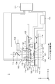
図1は、第1実施形態に係るインプリント装置1の構成を示す図である。鉛直方向の軸をZ軸、当該Z軸に垂直な平面内で互いに直交する2軸をX軸及びY軸としている。インプリント装置1は、基板101上のインプリント材102と型100との接触および引き離しによりパターンを形成する。型100は、立体形状のパターンが形成されたパターン面100aを有する。
[First Embodiment]
(Structure of imprint apparatus)
FIG. 1 is a diagram showing a configuration of an
照射部103は紫外線を出射し、型100とインプリント材102が接触している間にインプリント材102に照射することでインプリント材102を硬化させる。ミラー104は、照射部103から出射された紫外線を型100の方向に反射させる。供給部105は、未硬化状態のインプリント材102を基板101上に供給する。
The
インプリント装置1は、型100を保持する型保持部として、チャック106およびステージ107を有する。チャック106は、ステージ107上に配置されており、型100のパターン面100aとは反対側の面を、真空吸着力、静電気力、あるいは機械的手段により保持する。
The
ステージ107は、チャック106と共に型100を主にZ軸方向に沿って移動させる。これにより型100とインプリント材102とを接触させる動作(以下、押型動作という)、および型100とインプリント材102とを引き離す動作(以下、離型動作という)を行う。ステージ107は、基板101と型100との位置合わせの際に型100をX―Y平面内で移動させてもよい。ステージ107の駆動機構(不図示)として採用可能なアクチュエータとして、例えばボイスコイルモータやエアシリンダ等がある。チャック106とステージ107は一体の部材として構成されていてもよい。
The stage 107 moves the
インプリント装置1は、基板101を保持する基板保持部としてチャック108、およびステージ110を有する。当該基板保持部は、基板101を移動させる移動体でもある。
The
チャック108は、基板101を、真空吸着力、静電気力、あるいは機械的手段により基板101により保持する。
The
ステージ110は、とチャック108と基板101とを載せて主にX−Y平面内において移動する。図1は、ステージ110が型100と対向する位置(以下、インプリント位置という)で停止している様子を示している。ステージ110は、押型動作あるいは離型動作の際に、基板101をZ軸方向に移動させてもよい。ステージ107の駆動機構(不図示)に採用可能なアクチュエータとして、例えばボイスコイルモータやエアシリンダ等がある。
The
インプリント装置1は、基板101上の複数の被処理領域122(図2に図示)に対するインプリント材102の供給と供給されたインプリント材102に対するパターン形成とを、1つの被処理領域ずつ繰り返す。そのため、本実施形態に係るステージ110の主な移動方向は、供給部105と対向する位置から型100と対向する位置に向かう方向(X軸方向)である。
The
ステージ107およびステージ110は、微動ステージ及び当該微動ステージよりもストローク量の大きな粗動ステージとで構成されていてもよい。これにより、精度の良く型100あるいは基板101を位置決めすることができる。
The stage 107 and the
観察部111は、ミラー104を透過する波長の光を基板101に向けて透過し、基板101で反射された光を受光する。これにより、パターン面101aの凹凸構造へのインプリント材102の充填の様子を観察する。型100及び基板101には、パターン面101aの少なくとも四隅、および被処理領域の少なくとも四隅の位置を示すマーク(不図示)が形成されている。計測部112は、型100に形成されている前述のマークと基板101に形成されている前述のマークとを検出し、パターン面101aと基板101上の被処理領域122の相対位置を計測する。
The
気体吹き出し部113は、ステージ107およびチャック106の周囲に配置された環状の開口を有し、当該開口から−Z方向に向けて気体を供給する。これにより、インプリント装置1内で発生した異物がインプリント空間に進入することを低減している。なお、インプリント空間とは、気体吹き出し部113の内側の領域かつステージ110の移動する高さで規定される空間である。少なくとも、ステージ110がインプリント位置で停止した場合における、型100とステージ110との間の空間(型の下方の空間)を含む。
The gas blowing
定盤114は、気体吹き出し部113、供給部105、ステージ107を吊り下げ支持している。排気部115は、排気口115aと接続されており、気体吹き出し部113から供給された気体を排気する。構造体116には、ステージ107と、干渉計118が載置されている。干渉計118はレーザ光をステージ110の側面に配置されたミラー(不図示)に向けて照射し、当該ミラーで反射されたレーザ光を用いてステージ110の位置を計測する。
The
板部材(部材)117は、ステージ110上かつ、チャック108の周辺部(型保持部が基板を保持する部分)に配置されている。板部材117は、本実施形態のように基板101の表面に沿う方向(基板101を保持する保持面(基板の表面に沿う方向)に、チャック108の、基板101により被われる領域の外周を取り囲むような部材であることが好ましい。しかし、板部材117がチャック108の外周の一部を囲んでいない構成であっても構わない。
The plate member (member) 117 is arranged on the
本実施形態にかかる板部材117は、チャック108のすぐ隣にX軸方向に並列して配置された部材であるが、他の部材を介してチャック108の外周側に並列配置されていてもよい。板部材117は、後述のポリイミドの膜13と後述の電極群10とを有する。
The
電圧源119は、電極群10に対して電圧を印加する。これにより、電極群10を構成する電極ごとに、異なる極性の電位を与えることが可能である。電圧源119は、例えば、絶対値で300V〜3kV程度の電圧のうち、所定の直流電圧を電極群10に印加する。
The
気体供給部120は、周囲の気体とは異なる気体を供給する。少なくとも、ステージ110が基板101をインプリント位置に移動させる間に気体を供給する。例えば、気体供給部120が気体を供給する前の周囲の気体が空気である場合は、気体供給部120が供給する気体は、ヘリウム、窒素、凝縮性気体の少なくとも1種を供給するとよい。
The
板部材117は、ステージ110がインプリント位置へ向かう移動中に気体供給部120から供給された気体を型100と基板101との間の空間に導風する導風板としての機能も有する。空気から気体供給部120が供給する気体に置換することによって、パターン面100aに形成された凹凸面へのインプリント材102の充填促進や硬化パターンの欠陥を抑制する。
The
制御部121は、照射部103、ステージ110、観察部111、計測部112、気体吹き出し部113、干渉計118、電圧源129、排気部115と無線または優先で接続されている。
The
制御部121は、不図示の、CPUやメモリ(ROM、RAM)等を含む。当該メモリには例えば、後述の図6のフローチャートに示すインプリント工程に関するプログラム等が記憶されている。制御部121は、当該メモリ記憶されているプログラムに従って、制御部121に接続されている各構成部材を統括的に制御する。
The
制御部121は、制御部121が実行すべき機能を備えていれば、別個の制御基板の集合体であってもよいし、1つの制御基板であってもよい。
The
(電極群の構成)
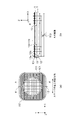
図2(a)(b)は、電極群10の構成を示す図である。図2(a)に示すように、板部材117は、電極群10を構成する電極として複数の電極を有する。複数の電極は、少なくとも、板部材117の領域(第1領域)10aに対応する位置に配置された電極(第1電極)11と板部材117の領域(第2領域)10bに対応する位置に配置された電極(第2電極)12とを有する。櫛歯状の電極11および電極12が、Y方向に交互に並ぶように配置されている。さらに、電極11と電極12の大部分(電極の半分以上の長さ)は、ステージ110の主な移動方向(X軸方向)に沿って延伸している。
(Configuration of electrode group)
2A and 2B are diagrams showing the configuration of the
なお、領域10aおよび領域10bは、板部材117の表面のうち、パターンの形成を行う空間109(図1に図示)に対向可能な面にある領域である。本実施形態では、パターン形成を行う空間109とは、型100と基板101とが対向する状態において型保持部の型100側かつ基板保持部の基板101側の空間である。すなわち、ステージ107の−Z方向側かつステージ110の+Z方向側の空間である。
The
図2(b)は図2(a)のA−A’断面図である。電圧源119は、電極11および電極12に電圧を印加する。特に、電圧源119は、電極11に電位を与えて領域10aを帯電させ、かつ、電極12に電極11とは異なる極性の電位を与えて領域10bを帯電させる。例えば図2(b)では、電極11が接地電位(0V)に対して負の電位を有し、電極12が接地電位に対して正の電位を有する様子を示している。電極11、電極12は、銅箔等の導体である。
2B is a cross-sectional view taken along the line A-A′ of FIG. The
さらに、電極11および電極12の表面は、ポリイミドの膜13で覆われている。膜13により、表面酸化等による劣化を防ぎ、かつ高電圧印加時の放電を防ぐことができる。誘電体であれば、膜13はポリイミド以外の材料でもよい。膜13のかわりに、電極11ごと、あるいは電極12ごとに、誘電体で覆う構成にしてもよい。
Further, the surfaces of the
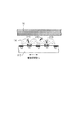
図3は、板部材117による異物の捕捉効果について説明する図である。電圧源119が、電極11を負に、電極12を正に帯電させると、電気力線14が電極12から電極11に向かう向きに電界が形成される。正に帯電した領域と負に帯電した領域とが交互になるように電圧源119が電圧を与えることにより、板部材117からのびた電気力線14が板部材117に向かうように閉じる電界が形成される。
FIG. 3 is a diagram for explaining the effect of capturing foreign matter by the
電極11、12の近傍において正に帯電した異物211は電気力線14に沿って電極11に向かうクーロン力を受ける。一方、負に帯電した異物212は電気力線14に沿って電極12に向かうクーロン力を受ける。さらに帯電していない状態の異物213は、電気力線が密になる方向に発生する静電気力の一種であるグラディエント力を受け、電極方向に引き寄せられる。
The positively charged
このように、互に異なる極性に帯電した領域10aと領域10bとを発生させることにより板部材117は異物の帯電状態に依存せず異物を捕捉することができる。よって、剥離動作によって型100が帯電したとしても、板部材117は、気体吹き出し部113による気体の流れ(クエット流ともいう)に逆らってステージ110の移動に伴い移動してくる異物を捕捉することができる。型100への異物の付着を低減し、型100と基板101との間における異物の挟み込みを低減できる。
In this way, the
それだけでなく、領域10aと領域10bとを互いに異なる極性に帯電した状態にすることで、板部材117から板部材117と対向する位置に存在する対向部材15に向かう電界が形成され難くできる。ここで、対向部材15とは、ステージ110が移動中に対向することになる部材であり、例えば、供給部105、チャック106、ステージ110、計測部112、定盤114等を含む。
Not only that, but by making the
対向部材15に向かう電界が形成されにくいことにより、板部材117上の異物が対向部材15への異物の付着を、領域10aと領域10bとを同じ極性に帯電させた場合に比べて低減することができる。よって、型100への付着による型100と基板101との間における異物の挟み込み、計測部112への付着による計測誤差、又は一度対向部材15に付着した異物の再浮遊等を防止または低減する効果を有する。
Since it is difficult to form an electric field toward the facing
パターン形成動作時(押型動作および離型動作)以外の時間帯の型100の待機位置の高さと、インプリント位置での板部材117の高さとの差に基づいて、電極11と電極12との距離Lが決定されていることが好ましい。
Based on the difference between the height of the standby position of the
例えば、電極12に電圧を+1kV印加し、電極11には−1kV印加する場合、パターン形成動作時以外の型100の待機位置の高さとインプリント位置での板部材117の高さとの差よりも、電極11と電極12との距離Lが短いほうが好ましい。電極11、12から+Z方向にL離れた位置では電位は0V程度になるため、板部材117から板部材117と対向部材15に向かう電界(+Z方向へ向かう電界)の発生を抑制することができる。
For example, when a voltage of +1 kV is applied to the
(実施例)
電極群10へ印加する電圧の違いによる対向部材15への異物の付着の違いについて説明する。図4は実験系の構成を示す図である。板部材117と対向部材15aを所定の間隔で離間配置させた状態で、供給部16が板部材117と対向部材15aとの間に向けて所定数の異物を含む気体を供給した。このとき、電極11および電極12に対して異なる極性の電圧(+1kVと−1kV)を印加した。さらに比較例として、電極11および電極12に対して同極性の電圧(+1kV)を印加した。その後、検査装置で対向部材15aに付着した異物を検出し、異物の個数を調べた。
(Example)
The difference in adhesion of foreign matter to the facing
図5(a)(b)は、実験結果を示す図である。図5(a)は電極11および電極12に対して異なる極性の電圧を印加した時の結果である。図5(b)は電極11および電極12に対して同極性の電圧(+1kV)を印加した時の結果を示している。対向部材15a内の黒い領域は、異物の付着箇所を示している。
5A and 5B are diagrams showing the experimental results. FIG. 5A shows the results when voltages of different polarities were applied to the
図5に示すように、電極11および電極12に対して異なる極性の電圧を印加した場合の方が、同極性の電圧を印加した場合よりも対向部材15aへの異物の付着量を抑制できることが確認できた。電極11および電極12に対して異なる極性の電圧を印加した場合は、比較例の場合に比べて対向部材15aに付着した異物の個数は、1/5以下であった。
As shown in FIG. 5, when the voltages of different polarities are applied to the
(インプリント方法)
図6は、インプリント装置1によるインプリント方法を示すフローチャート210である。まず、電圧源119が板部材117上の電極群10に対して電圧を印加する(S201)。これにより、電極11と電極12に異なる極性の電位を与えるように、電極11と電極12を帯電させる。制御部121は、搬送機構(不図示)を制御して型100および基板101をインプリント装置1内に搬入する(S202)。ステージ110が最初の被処理領域122を供給位置に移動させ、供給部105がインプリント材102を供給する(S203)。
(Imprint method)
FIG. 6 is a
つづいて、被処理領域に対してパターンを形成する(S204)。S204の工程は、インプリント材102と型100との接触動作、照射部103によるインプリント材102の硬化動作、インプリント材102と型100との引き離し動作を有する。
Subsequently, a pattern is formed in the processing target area (S204). The step S204 includes a contact operation between the
制御部121が次にパターンを形成すべき被処理領域122があるかを判断し(S205)、あると判断した場合はS203〜S205の工程を繰り返す。次の被処理領域122がない場合は、型100および基板101をインプリント装置1から搬出する(S206)。最後に、電圧源119は電極11と電極12に対する電圧の印加を停止し、帯電状態を停止させる(S207)。
The
インプリント装置1は、所定のロット毎、あるいは所定の基板枚数毎に、型100に付着した可能性のある異物のクリーニング動作を行ってもよい。板部材117と型100が対向する位置で板部材117と型100との相対距離が縮まるように板部材117を+Z方向に上昇させる工程を行っても良い。このとき、型100の電位を計測し、計測結果よりも大きな絶対値の電圧が電極群10に印加されていることが好ましい。
The
クリーニング動作を行うことにより、一度パターン面101aに付着してしまった異物を板部材117側に引き寄せて、捕捉することができる。よって、パターン形成の際に、型100と基板101との間における異物の挟み込みを低減し、パターン欠陥の発生や型100の破損を低減することができる。
By performing the cleaning operation, the foreign matter once attached to the
[第2実施形態]
図7(a)(b)は、電極群10の、第1実施形態で示した構成とは異なる構成を示す図である。電極11、12の主な配列方向は、ステージ110の主な移動方向に沿う方向に延伸していてもよいし(図7(a))、ステージ110の主な移動方向に直交する方向に沿う方向(主な移動方向に交差する方向)に延伸していてもよい(図7(b))。
[Second Embodiment]
7A and 7B are diagrams showing a configuration of the
いずれの場合も、板部材117は異物を捕捉しつつ、対向部材15に対する異物の付着を電極11および電極12に同極性の電圧を印加した場合に比べて低減することができる。より好ましくは、電極11、12が、ステージ110の主な移動方向に沿う方向に延伸している場合である。
In any case, the
図8は、電極11、12の延伸方向とステージ110の移動方向にそって浮遊する異物の挙動の関係を示す第1図である。特に、電極11、12が、ステージ110の主な移動方向に沿う方向に延伸している場合の異物の挙動を示している。ステージ110の主な移動方向と電極11、12の延伸方向が平行なため、異物200は部材15と板部材117との間を一定の電界を受けながら進む。
FIG. 8 is a first diagram showing the relationship between the extending directions of the
例えば、電極12の場合は負に帯電した異物212はX軸方向には常に一方向の静電気力をうけやすくなるため、放物線を描いたような軌跡を描きながら電極12に近づき、電極12の付近の領域で捕捉される。同様にして、電極11によって正に帯電した異物が捕捉される。
For example, in the case of the
図9は、電極11、12の延伸方向とステージ110の移動方向にそって浮遊する異物の挙動の関係を示す第2図である。電極11、12の主な延伸方向が、ステージ110の主な移動方向に直交する方向に沿う方向に延伸している場合の異物の挙動を示している。図9に示すように異物200は部材15と板部材117との間を交互に異なる方向の電界を受けながら進む。そのため、ステージ110の移動方向に沿って進む異物200は、電極11、12が、ステージ110の主な移動方向に沿う方向に延伸している場合に比べて板部材117に捕捉されにくくなる恐れがあるからである。
FIG. 9 is a second diagram showing the relationship between the extending directions of the
[第3実施形態]
異物捕捉用の板部材は、次の(1)(2)うち、少なくとも一方であればよい。(1)型保持部の、型100の表面に沿う方向に型100により被われる領域の外周を取り囲むように配置された部材(2)基板保持部の、基板101の表面に沿う方向に基板101により被われる領域の外周を取り囲むように配置された部材。図10は、型保持部上に配置された板部材130の構成を示す図である。板部材130上には電極21および電極20を交互に配置した電極群20が配置されている。
[Third Embodiment]
The plate member for capturing the foreign matter may be at least one of the following (1) and (2). (1) A member arranged so as to surround the outer periphery of a region covered by the
電極21および電極20を互いに異なる極性に帯電させることにより、電極21の付近の領域および電極22の付近の領域が異なる極性に帯電した状態となる。これにより、板部材130は、板部材130に捕捉しつつ、板部材130と対向する部材に対する異物の付着を低減することができる。すなわち、基板101に対する異物の付着を抑制することができる。
By charging the
なお、電極20、21は型100の表面に沿う方向(型100を保持する保持面に沿う方向)に、型100により被われる領域の外周を取り囲むような部材であることが好ましいが、これ以外の構成であってもよい。
The
[第4実施形態]
ステージ110は他のリソグラフィ装置に搭載してもよい。リソグラフィ装置として、例えば、i線、KrFレーザ光、EUV光等の光線を照射することにより、基板上にレジストによる潜像パターンを形成する露光装置に搭載してもよい。図11は、ステージ110が搭載された、露光装置150の構成を示す図である。インプリント装置1と同じ構成部材には同じ符号を付している。
[Fourth Embodiment]
The
レチクル(物体、原版)160には回路パターンが形成されおり、かつ異物付着防止用に透明な保護膜(ペリクル膜)が配置されている。レチクル160を保持する保持部として、チャック161およびレチクルステージ165を有する。チャック161はレチクルを、静電気力、真空吸着力、または機械的保持手段により保持する。
A circuit pattern is formed on the reticle (object, original plate) 160, and a transparent protective film (pellicle film) is arranged to prevent foreign matter from adhering. A
板部材163は、レチクル160を保持する部分の周辺部に配置された部材である。板部材163には、電極群164が配置されている。レチクルステージ165は、レチクル160およびチャック161と共にX軸方向にスキャン動作する。干渉計118はレチクルステージ165の位置を計測する干渉計である。構造体167はレチクルステージ165を支持している。
The
照明系170は、レチクル160のパターンを照明する。投影系(光学系)171は、照明系170によって照明されたレチクル160のパターンを基板101上に縮小投影する。補正手段172は投影系171における投影像の倍率、ディストーション、などを補正する手段である。構造体173は投影系171を支持している。スコープ174は基板101の位置を計測する。計測系175は基板101の高さおよび傾斜を計測する。
The
制御部180は、照明系170、干渉計118、電圧源119、168、補正手段172、スコープ174、計測系175と接続されており、これらを制御する。露光装置150は、ステージ110が基板101をX軸方向に走査させている最中にレチクル160も基板101の駆動に同期させながらX軸方向に走査させる。
The
電極群164は、複数の電極を有する。制御部180は電圧源168を制御して、電極群164の第1の電極と第2の電極とが異なる極性に帯電するように電圧を印加する。すなわち、レチクルの周囲に互いに異なる極性に帯電した2つの領域を形成する。板部材163上にも互いに異なる極性に帯電した二つの領域を形成する。
The
これにより、板部材117上を同じ極性のみに帯電させた場合に比べて対向部材への異物の付着を低減することができる。板部材117に対する対向部材とは、例えば、構造体173、投影系171、スコープ174等である。さらに板部材163上を同じ極性のみに帯電させた場合に比べて対向部材への異物の付着を低減することができる。板部材163に対する対向部材とは、例えば、照明系170である。
As a result, the adhesion of foreign matter to the facing member can be reduced as compared with the case where the
よって、例えば照明系170や投影系171の最終レンズへの異物付着に起因して生じうる、形成されるパターンの欠陥を抑制できる。また、異物を捕捉することができるため、レチクル160や基板101等への異物の付着を抑制できる。
Therefore, it is possible to suppress defects in the formed pattern that may be caused by, for example, adhesion of foreign matter to the final lens of the
[ステージの主な移動方向]
ステージ110は、各動作の最中に様々な方向に移動する。ステージ110の移動方向および距離を考慮して、ステージ110の主な移動方向を決定するとよい。ステージ110の主な移動方向の一例について図12〜図13を用いて説明する。図12は、演算時の定義を説明する図である。型100の中心を原点Oとし、ステージ110のさまざまな移動を2点間の移動に分割する。ある動作において、ステージ110が位置Pb(b1、b2)から位置Pa(a1、a1)に向かう時の移動距離をDi、X軸に対してなす角をθiとする。
[Main movement direction of stage]
The
ステージ110の動作ごとにDiおよびθiを算出し、同一のθiに対するそれぞれのDiの合計ΣDiの関数を作成する。図13は、θiとΣDiとの関係を示す図である。ΣDiが最大となる、所定の角度θnの方向がステージ110の主な移動方向である。電極群10の配置する際に、このようにして算出した方向に沿う方向に電極11、12が延伸するように配置するとよい。インプリント装置1においては、この角度θnが、前述した供給部105から型100からインプリント位置に向かう方向(X軸方向)となる。
Di and θi are calculated for each operation of the
露光装置150においても、インプリント装置1の場合と同様の算出方法でステージの主な移動方向は決定される。露光装置150の場合、計測系175やスコープ174による計測動作に伴う移動の、移動方向および移動距離も考慮する。露光装置150の場合、レチクルステージ165の主な移動方向およびステージ110の主な移動方向はX軸方向である。したがって、電極群164が有する電極の延伸方向とレチクルステージ165との方向は平行にすることがより好ましい。電極群10が有する電極の延伸方向はステージ110の主な移動方向に沿う方向であることが好ましい。
Also in the
この他にも、各装置での一連のステージ動作の中で、X軸方向の積算移動距離とY軸方向の積算移動距離を比較して積算移動距離が大きい軸の方向を主要な動作方向としてもよい。また、ステージ速度も異物の挙動に影響するため、ステージ速度とステージ移動方向を組み合わせた評価関数を用いてステージの主な移動方向を決定してもよい。 In addition to this, in a series of stage operations in each device, the accumulated movement distance in the X-axis direction and the accumulated movement distance in the Y-axis direction are compared, and the direction of the axis having the larger accumulated movement distance is set as the main movement direction. Good. Further, since the stage speed also affects the behavior of the foreign matter, the main moving direction of the stage may be determined using an evaluation function that combines the stage speed and the stage moving direction.
[その他の実施形態]
型保持部、基板保持部、レチクル160を保持する保持部などが、それぞれの保持対象物(物体)の外周のみを保持する場合もありうる。このような場合、当該保持対象物により被われる領域の周辺の領域とは、型保持部、基板保持部、レチクル160を保持する保持部のそれぞれの、保持対象物の外側の領域を意味する。
[Other Embodiments]
The die holding unit, the substrate holding unit, the holding unit holding the
電極群10の構成は、前述の実施形態に限られない。基板101の配置位置に対して同心上に電極11および電極12が交互に配列されていてもよい。あるいは基板101を保持する部分を取り囲むような、矩形の電極11と矩形の電極12とが交互に配列された構成でもよい。電極群10は、1本の電極11、12ごとに電圧の印加の有無を制御可能な配線でもよい。所定本数毎の電極に電圧を印加しないことによって、帯電状態の電極11同士の間隔および帯電状態の電極12同士の間隔を調整してもよい。印加する電圧の大きさを、型100の帯電度合に応じて変更してもよい。
The configuration of the
電極群10および電圧源19のかわりに、エレクトレット樹脂等の、常に帯電している状態の材料を配置してもよい。このとき、それぞれが異なる極性に帯電している少なくとも2つの帯電材料を配置することが好ましい。
Instead of the
本明細書において、「異物」とは、パターン形成に関与することを目的としていない物質である。例えば、供給部105により吐出されたインプリント材102がミストとして漂い乾燥した固形物、インプリント装置1を構成する部材から生じる微粒子、外部空間から進入してインプリント装置1内に存在する塵などである。
In the present specification, the “foreign substance” is a substance that is not intended to participate in pattern formation. For example, the
インプリント装置1で使用するインプリント材102および露光装置150で使用するレジストには、硬化用のエネルギーが与えられることにより硬化する硬化性組成物(未硬化状態の樹脂と呼ぶこともある)が用いられる。硬化用のエネルギーとしては、電磁波、熱等が用いられる。電磁波としては、例えば、その波長が10nm以上1mm以下の範囲から選択される、赤外線、可視光線、紫外線などの光である。
The
硬化性組成物は、光の照射により、あるいは、加熱により硬化する組成物である。このうち、光により硬化する光硬化性組成物は、重合性化合物と光重合開始剤とを少なくとも含有し、必要に応じて非重合性化合物または溶剤を含有してもよい。非重合性化合物は、増感剤、水素供与体、内添型離型剤、界面活性剤、酸化防止剤、ポリマー成分などの群から選択される少なくとも一種である。 The curable composition is a composition that is cured by irradiation with light or by heating. Among these, the photocurable composition that is cured by light contains at least a polymerizable compound and a photopolymerization initiator, and may contain a non-polymerizable compound or a solvent as necessary. The non-polymerizable compound is at least one selected from the group consisting of a sensitizer, a hydrogen donor, an internal release agent, a surfactant, an antioxidant and a polymer component.
インプリント材102は、スピンコーターやスリットコーターにより基板上に膜状に付与される。或いは液体噴射ヘッドにより、液滴状、或いは複数の液滴が繋がってできた島状又は膜状となって基板上に付与されてもよい。インプリント材102の粘度(25℃における粘度)は、例えば、1mPa・s以上100mPa・s以下である。
The
[物品の製造方法]
前述の各実施形態に係るリソグラフィ装置で基板上に形成した硬化物のパターンは、各種物品の少なくとも一部に恒久的に、或いは各種物品を製造する際に一時的に、用いられる。
[Production method]
The pattern of the cured product formed on the substrate by the lithographic apparatus according to each of the above-described embodiments is used for at least a part of various articles permanently or temporarily when manufacturing various articles.
基板は、ガラス、セラミックス、金属、半導体、樹脂等が用いられ、必要に応じて、その表面に基板とは別の材料からなる部材が形成されていてもよい。基板は、具体的には、シリコンウエハ、化合物半導体ウエハ、石英ガラス等である。 The substrate is made of glass, ceramics, metal, semiconductor, resin or the like, and a member made of a material different from that of the substrate may be formed on the surface of the substrate, if necessary. The substrate is specifically a silicon wafer, a compound semiconductor wafer, quartz glass, or the like.
物品とは、電気回路素子、光学素子、MEMS、記録素子、センサ、或いは、型等である。電気回路素子としては、DRAM、SRAM、フラッシュメモリ、MRAMのような、揮発性或いは不揮発性の半導体メモリや、LSI、CCD、イメージセンサ、FPGAのような半導体素子等が挙げられる。型としては、インプリント用の型(パターンが複製される側の型)等が挙げられる。 The article is an electric circuit element, an optical element, a MEMS, a recording element, a sensor, a mold, or the like. Examples of the electric circuit element include volatile or non-volatile semiconductor memory such as DRAM, SRAM, flash memory and MRAM, and semiconductor elements such as LSI, CCD, image sensor and FPGA. Examples of the mold include an imprint mold (a mold on the side where the pattern is duplicated) and the like.
硬化物のパターンは、上記物品の少なくとも一部の構成部材として、そのまま用いられるか、或いは、レジストマスクとして一時的に用いられる。基板の加工工程においてエッチング又はイオン注入等が行われた後、レジストマスクは除去される。加工工程はさらに、他の周知の処理工程(現像、酸化、成膜、蒸着、平坦化、レジスト剥離、ダイシング、ボンディング、パッケージング等)を含んでもよい。 The pattern of the cured product is used as it is as a constituent member of at least a part of the article, or is temporarily used as a resist mask. The resist mask is removed after etching or ion implantation is performed in the substrate processing step. The processing step may further include other known processing steps (development, oxidation, film formation, vapor deposition, planarization, resist stripping, dicing, bonding, packaging, etc.).
以上、本発明の好ましい実施形態について説明したが、本発明はこれらの実施形態に限定されないことはいうまでもなく、その要旨の範囲内で種々の変形及び変更が可能である。 Although the preferred embodiments of the present invention have been described above, it goes without saying that the present invention is not limited to these embodiments, and various modifications and changes can be made within the scope of the gist thereof.
100 型
101 基板
106 チャック(型保持部)
107 ステージ(型保持部)
108 チャック(基板保持部)
110 ステージ(基板保持部)
104 インプリント材
10a 第1領域
10b 第2領域
100
107 stage (mold holding unit)
108 chuck (substrate holder)
110 stage (substrate holder)
104
Claims (11)
前記型を保持する型保持部と、
前記基板を保持する基板保持部と、を有し、
前記基板保持部の前記基板により被われる領域の周辺領域に、互いに異なる極性に帯電した第1領域と第2領域とを発生させるように設けられ、
前記第1領域および前記第2領域は、前記基板の表面に沿う方向に、前記基板により被われる領域の外周を取り囲むように配置されていることを
特徴とするインプリント装置。 An imprint apparatus for forming a pattern of an imprint material on a substrate using a mold,
A mold holding unit for holding the mold,
A substrate holding unit for holding the substrate,
Around area of the region covered by the substrate prior Symbol substrate holder provided so that to generate a first region and a second region which is oppositely charged,
The imprint apparatus, wherein the first region and the second region are arranged in a direction along a surface of the substrate so as to surround an outer periphery of a region covered by the substrate .
前記型を保持する型保持部と、A mold holding unit for holding the mold,
前記基板を保持する基板保持部と、を有し、A substrate holding unit for holding the substrate,
前記型保持部の前記型により被われる領域の周辺領域に、互いに異なる極性に帯電した第1領域と第2領域とを発生させるように設けられ、The mold holding portion is provided in a peripheral region of a region covered by the mold so as to generate a first region and a second region charged with polarities different from each other,
前記第1領域および前記第2領域は、前記型の表面に沿う方向に、前記型により被われる領域の外周を取り囲むように配置されていることをThe first region and the second region are arranged in a direction along the surface of the mold so as to surround the outer periphery of the region covered by the mold.
特徴とするインプリント装置。Characteristic imprinting device.
前記第2領域に対応する位置に配置された第2電極と、
電圧源をさらに有し、
前記電圧源は、前記第1電極に電位を与えて前記第1領域を帯電させ、かつ、前記第2電極に前記第1電極とは異なる極性の電位を与えて前記第2領域を帯電させることを特徴とする請求項1または2に記載のインプリント装置。 A first electrode arranged at a position corresponding to the first region,
A second electrode arranged at a position corresponding to the second region;
Further having a voltage source,
The voltage source applies a potential to the first electrode to charge the first region, and applies a potential having a polarity different from that of the first electrode to the second electrode to charge the second region. The imprint apparatus according to claim 1 or 2 , characterized in that:
前記第1電極および前記第2電極は、前記基板保持部の移動方向に沿う方向に延伸していることを特徴とする請求項3に記載のインプリント装置。 The substrate holder is movable while holding the substrate,
The imprint apparatus according to claim 3 , wherein the first electrode and the second electrode extend in a direction along a moving direction of the substrate holding unit.
前記第1領域と前記第2領域は、前記導風板の表面に位置することを特徴とする請求項1乃至5のいずれか1項に記載のインプリント装置。 The substrate holding unit has a baffle plate that guides the gas supplied from the gas supply unit into the space between the mold and the substrate,
The imprint apparatus according to any one of claims 1 to 5 , wherein the first area and the second area are located on a surface of the baffle plate.
前記工程でパターンの形成された前記基板を加工する工程と、を有することを特徴とする物品の製造方法。 Forming a pattern of an imprint material on the substrate by using the imprint apparatus according to any one of claims 1 to 7 ;
A step of processing the substrate on which the pattern is formed in the step, and a method for manufacturing an article.
前記原版を保持する原版保持部と、
前記基板を保持する基板保持部と、を有し、
前記基板保持部の前記基板により被われる領域の周辺領域に、互いに異なる極性に帯電した第1領域と第2領域とを発生させるように設けられ、
前記第1領域および前記第2領域は、前記基板の表面に沿う方向に、前記基板により被われる領域の外周を取り囲むように配置されていることを
特徴とする露光装置。 An optical system that projects the pattern formed on the original onto the substrate,
An original holding unit for holding the original,
A substrate holding unit for holding the substrate,
Around area of the region covered by the substrate prior Symbol substrate holding portion provided so as to generate a first region and a second region which is oppositely charged,
The exposure apparatus, wherein the first region and the second region are arranged in a direction along a surface of the substrate so as to surround an outer periphery of a region covered by the substrate .
前記原版を保持する原版保持部と、An original holding unit for holding the original,
前記基板を保持する基板保持部と、を有し、A substrate holding unit that holds the substrate,
前記原版保持部の前記原版により被われる領域の周辺領域に、互いに異なる極性に帯電した第1領域と第2領域とを発生させるように設けられ、The area around the area of the original holding portion covered by the original is provided so as to generate a first area and a second area charged with polarities different from each other.
前記第1領域および前記第2領域は、前記原版の表面に沿う方向に、前記原版により被われる領域の外周を取り囲むように配置されていることをThe first region and the second region are arranged in a direction along the surface of the original plate so as to surround the outer periphery of the region covered by the original plate.
特徴とする露光装置。Characteristic exposure equipment.
Priority Applications (2)
| Application Number | Priority Date | Filing Date | Title |
|---|---|---|---|
| JP2016038129A JP6732475B2 (en) | 2016-02-29 | 2016-02-29 | Imprint apparatus, article manufacturing method, holding apparatus, and exposure apparatus |
| US15/436,635 US10889052B2 (en) | 2016-02-29 | 2017-02-17 | Imprint apparatus, method for manufacturing article, and exposure apparatus |
Applications Claiming Priority (1)
| Application Number | Priority Date | Filing Date | Title |
|---|---|---|---|
| JP2016038129A JP6732475B2 (en) | 2016-02-29 | 2016-02-29 | Imprint apparatus, article manufacturing method, holding apparatus, and exposure apparatus |
Publications (3)
| Publication Number | Publication Date |
|---|---|
| JP2017157640A JP2017157640A (en) | 2017-09-07 |
| JP2017157640A5 JP2017157640A5 (en) | 2019-04-11 |
| JP6732475B2 true JP6732475B2 (en) | 2020-07-29 |
Family
ID=59679216
Family Applications (1)
| Application Number | Title | Priority Date | Filing Date |
|---|---|---|---|
| JP2016038129A Active JP6732475B2 (en) | 2016-02-29 | 2016-02-29 | Imprint apparatus, article manufacturing method, holding apparatus, and exposure apparatus |
Country Status (2)
| Country | Link |
|---|---|
| US (1) | US10889052B2 (en) |
| JP (1) | JP6732475B2 (en) |
Families Citing this family (1)
| Publication number | Priority date | Publication date | Assignee | Title |
|---|---|---|---|---|
| JP6735656B2 (en) * | 2016-11-18 | 2020-08-05 | キヤノン株式会社 | Imprint apparatus, imprint method, and article manufacturing method |
Family Cites Families (7)
| Publication number | Priority date | Publication date | Assignee | Title |
|---|---|---|---|---|
| DE60118669T2 (en) * | 2000-08-25 | 2007-01-11 | Asml Netherlands B.V. | Lithographic projection apparatus |
| JP2006120776A (en) * | 2004-10-20 | 2006-05-11 | Canon Inc | Exposure apparatus |
| JP5647029B2 (en) * | 2011-02-18 | 2014-12-24 | キヤノン株式会社 | Imprint apparatus and article manufacturing method |
| JP5818962B2 (en) | 2011-03-23 | 2015-11-18 | エスアールアイ インターナショナルSRI International | Active electroadhesive cleaning |
| JP6171412B2 (en) * | 2013-03-06 | 2017-08-02 | 大日本印刷株式会社 | Imprint method, imprint mold and imprint apparatus |
| JP6123396B2 (en) * | 2013-03-18 | 2017-05-10 | 大日本印刷株式会社 | Imprint method and imprint apparatus |
| JP6643135B2 (en) * | 2016-02-17 | 2020-02-12 | キヤノン株式会社 | Lithographic apparatus and article manufacturing method |
-
2016
- 2016-02-29 JP JP2016038129A patent/JP6732475B2/en active Active
-
2017
- 2017-02-17 US US15/436,635 patent/US10889052B2/en active Active
Also Published As
| Publication number | Publication date |
|---|---|
| JP2017157640A (en) | 2017-09-07 |
| US20170246792A1 (en) | 2017-08-31 |
| US10889052B2 (en) | 2021-01-12 |
Similar Documents
| Publication | Publication Date | Title |
|---|---|---|
| US9188854B2 (en) | Transfer apparatus and method of manufacturing device | |
| TWI649183B (en) | Imprinting device, imprinting method, and method of manufacturing the article | |
| JP2015149390A (en) | Imprint device, die, and method of manufacturing article | |
| JP2017147343A (en) | Lithography apparatus and article manufacturing method | |
| KR102134212B1 (en) | Imprint apparatus, imprint method and article manufacturing method | |
| JP7261000B2 (en) | CONTAINER, PROCESSING APPARATUS, CONTENT REMOVAL METHOD, AND PRODUCT MANUFACTURING METHOD | |
| WO2016170729A1 (en) | Imprint apparatus, method of imprinting, and method of manufacturing article | |
| KR102206846B1 (en) | Imprint apparatus and article manufacturing method | |
| US10777443B2 (en) | Imprint apparatus, imprinting method, and method for manufacturing article | |
| JP6732475B2 (en) | Imprint apparatus, article manufacturing method, holding apparatus, and exposure apparatus | |
| KR102543393B1 (en) | Information processing apparatus, storage medium, lithography apparatus, lithography system, and article manufacturing method | |
| JP2017139452A (en) | Imprint apparatus and method of manufacturing article | |
| KR102179737B1 (en) | Imprint apparatus, imprint method, and article manufacturing method | |
| JP6942562B2 (en) | Lithography equipment and manufacturing method of goods | |
| JP6603678B2 (en) | Imprint apparatus, operation method thereof, and article manufacturing method | |
| JP2020013890A (en) | Imprint device, control method thereof, and article manufacturing method | |
| JP7089420B2 (en) | Substrate processing equipment and article manufacturing method | |
| KR20170054455A (en) | Imprint apparatus, imprint method, and article manufacturing method | |
| JP2019067916A (en) | Lithography apparatus and method of manufacturing article | |
| JP6884048B2 (en) | Imprint equipment and article manufacturing method | |
| US20230347391A1 (en) | Foreign particle removing method, formation method, article manufacturing method, foreign particle removing apparatus, system, and template | |
| JP2021002626A (en) | Imprint device and manufacturing method for article | |
| WO2017149992A1 (en) | Imprinting device, imprinting method and article production method | |
| JP2019117845A (en) | Lithographic apparatus and article manufacturing method | |
| WO2017134989A1 (en) | Imprinting device, and article production method |
Legal Events
| Date | Code | Title | Description |
|---|---|---|---|
| A521 | Request for written amendment filed |
Free format text: JAPANESE INTERMEDIATE CODE: A523 Effective date: 20190226 |
|
| A621 | Written request for application examination |
Free format text: JAPANESE INTERMEDIATE CODE: A621 Effective date: 20190226 |
|
| A977 | Report on retrieval |
Free format text: JAPANESE INTERMEDIATE CODE: A971007 Effective date: 20191127 |
|
| A131 | Notification of reasons for refusal |
Free format text: JAPANESE INTERMEDIATE CODE: A131 Effective date: 20191210 |
|
| A521 | Request for written amendment filed |
Free format text: JAPANESE INTERMEDIATE CODE: A523 Effective date: 20200204 |
|
| TRDD | Decision of grant or rejection written | ||
| A01 | Written decision to grant a patent or to grant a registration (utility model) |
Free format text: JAPANESE INTERMEDIATE CODE: A01 Effective date: 20200609 |
|
| A61 | First payment of annual fees (during grant procedure) |
Free format text: JAPANESE INTERMEDIATE CODE: A61 Effective date: 20200708 |
|
| R151 | Written notification of patent or utility model registration |
Ref document number: 6732475 Country of ref document: JP Free format text: JAPANESE INTERMEDIATE CODE: R151 |