JP6735656B2 - Imprint apparatus, imprint method, and article manufacturing method - Google Patents
Imprint apparatus, imprint method, and article manufacturing method Download PDFInfo
- Publication number
- JP6735656B2 JP6735656B2 JP2016225375A JP2016225375A JP6735656B2 JP 6735656 B2 JP6735656 B2 JP 6735656B2 JP 2016225375 A JP2016225375 A JP 2016225375A JP 2016225375 A JP2016225375 A JP 2016225375A JP 6735656 B2 JP6735656 B2 JP 6735656B2
- Authority
- JP
- Japan
- Prior art keywords
- mold
- gas
- substrate
- imprint
- imprint material
- Prior art date
- Legal status (The legal status is an assumption and is not a legal conclusion. Google has not performed a legal analysis and makes no representation as to the accuracy of the status listed.)
- Active
Links
Images


Classifications
-
- G—PHYSICS
- G03—PHOTOGRAPHY; CINEMATOGRAPHY; ANALOGOUS TECHNIQUES USING WAVES OTHER THAN OPTICAL WAVES; ELECTROGRAPHY; HOLOGRAPHY
- G03F—PHOTOMECHANICAL PRODUCTION OF TEXTURED OR PATTERNED SURFACES, e.g. FOR PRINTING, FOR PROCESSING OF SEMICONDUCTOR DEVICES; MATERIALS THEREFOR; ORIGINALS THEREFOR; APPARATUS SPECIALLY ADAPTED THEREFOR
- G03F7/00—Photomechanical, e.g. photolithographic, production of textured or patterned surfaces, e.g. printing surfaces; Materials therefor, e.g. comprising photoresists; Apparatus specially adapted therefor
- G03F7/0002—Lithographic processes using patterning methods other than those involving the exposure to radiation, e.g. by stamping
-
- B—PERFORMING OPERATIONS; TRANSPORTING
- B05—SPRAYING OR ATOMISING IN GENERAL; APPLYING FLUENT MATERIALS TO SURFACES, IN GENERAL
- B05C—APPARATUS FOR APPLYING FLUENT MATERIALS TO SURFACES, IN GENERAL
- B05C9/00—Apparatus or plant for applying liquid or other fluent material to surfaces by means not covered by any preceding group, or in which the means of applying the liquid or other fluent material is not important
- B05C9/08—Apparatus or plant for applying liquid or other fluent material to surfaces by means not covered by any preceding group, or in which the means of applying the liquid or other fluent material is not important for applying liquid or other fluent material and performing an auxiliary operation
-
- B—PERFORMING OPERATIONS; TRANSPORTING
- B29—WORKING OF PLASTICS; WORKING OF SUBSTANCES IN A PLASTIC STATE IN GENERAL
- B29C—SHAPING OR JOINING OF PLASTICS; SHAPING OF MATERIAL IN A PLASTIC STATE, NOT OTHERWISE PROVIDED FOR; AFTER-TREATMENT OF THE SHAPED PRODUCTS, e.g. REPAIRING
- B29C59/00—Surface shaping of articles, e.g. embossing; Apparatus therefor
- B29C59/02—Surface shaping of articles, e.g. embossing; Apparatus therefor by mechanical means, e.g. pressing
-
- G—PHYSICS
- G03—PHOTOGRAPHY; CINEMATOGRAPHY; ANALOGOUS TECHNIQUES USING WAVES OTHER THAN OPTICAL WAVES; ELECTROGRAPHY; HOLOGRAPHY
- G03F—PHOTOMECHANICAL PRODUCTION OF TEXTURED OR PATTERNED SURFACES, e.g. FOR PRINTING, FOR PROCESSING OF SEMICONDUCTOR DEVICES; MATERIALS THEREFOR; ORIGINALS THEREFOR; APPARATUS SPECIALLY ADAPTED THEREFOR
- G03F7/00—Photomechanical, e.g. photolithographic, production of textured or patterned surfaces, e.g. printing surfaces; Materials therefor, e.g. comprising photoresists; Apparatus specially adapted therefor
- G03F7/16—Coating processes; Apparatus therefor
- G03F7/168—Finishing the coated layer, e.g. drying, baking, soaking
-
- G—PHYSICS
- G03—PHOTOGRAPHY; CINEMATOGRAPHY; ANALOGOUS TECHNIQUES USING WAVES OTHER THAN OPTICAL WAVES; ELECTROGRAPHY; HOLOGRAPHY
- G03F—PHOTOMECHANICAL PRODUCTION OF TEXTURED OR PATTERNED SURFACES, e.g. FOR PRINTING, FOR PROCESSING OF SEMICONDUCTOR DEVICES; MATERIALS THEREFOR; ORIGINALS THEREFOR; APPARATUS SPECIALLY ADAPTED THEREFOR
- G03F7/00—Photomechanical, e.g. photolithographic, production of textured or patterned surfaces, e.g. printing surfaces; Materials therefor, e.g. comprising photoresists; Apparatus specially adapted therefor
- G03F7/70—Microphotolithographic exposure; Apparatus therefor
- G03F7/708—Construction of apparatus, e.g. environment aspects, hygiene aspects or materials
- G03F7/70808—Construction details, e.g. housing, load-lock, seals or windows for passing light in or out of apparatus
- G03F7/70825—Mounting of individual elements, e.g. mounts, holders or supports
-
- H—ELECTRICITY
- H01—ELECTRIC ELEMENTS
- H01L—SEMICONDUCTOR DEVICES NOT COVERED BY CLASS H10
- H01L21/00—Processes or apparatus adapted for the manufacture or treatment of semiconductor or solid state devices or of parts thereof
- H01L21/02—Manufacture or treatment of semiconductor devices or of parts thereof
- H01L21/027—Making masks on semiconductor bodies for further photolithographic processing not provided for in group H01L21/18 or H01L21/34
- H01L21/0271—Making masks on semiconductor bodies for further photolithographic processing not provided for in group H01L21/18 or H01L21/34 comprising organic layers
-
- H—ELECTRICITY
- H01—ELECTRIC ELEMENTS
- H01L—SEMICONDUCTOR DEVICES NOT COVERED BY CLASS H10
- H01L21/00—Processes or apparatus adapted for the manufacture or treatment of semiconductor or solid state devices or of parts thereof
- H01L21/67—Apparatus specially adapted for handling semiconductor or electric solid state devices during manufacture or treatment thereof; Apparatus specially adapted for handling wafers during manufacture or treatment of semiconductor or electric solid state devices or components ; Apparatus not specifically provided for elsewhere
- H01L21/67005—Apparatus not specifically provided for elsewhere
- H01L21/67011—Apparatus for manufacture or treatment
- H01L21/67017—Apparatus for fluid treatment
- H01L21/67063—Apparatus for fluid treatment for etching
-
- G—PHYSICS
- G03—PHOTOGRAPHY; CINEMATOGRAPHY; ANALOGOUS TECHNIQUES USING WAVES OTHER THAN OPTICAL WAVES; ELECTROGRAPHY; HOLOGRAPHY
- G03F—PHOTOMECHANICAL PRODUCTION OF TEXTURED OR PATTERNED SURFACES, e.g. FOR PRINTING, FOR PROCESSING OF SEMICONDUCTOR DEVICES; MATERIALS THEREFOR; ORIGINALS THEREFOR; APPARATUS SPECIALLY ADAPTED THEREFOR
- G03F7/00—Photomechanical, e.g. photolithographic, production of textured or patterned surfaces, e.g. printing surfaces; Materials therefor, e.g. comprising photoresists; Apparatus specially adapted therefor
- G03F7/70—Microphotolithographic exposure; Apparatus therefor
- G03F7/70691—Handling of masks or workpieces
- G03F7/70716—Stages
Description
本発明は、インプリント装置、インプリント方法及び物品の製造方法に関する。 The present invention relates to an imprint apparatus, an imprint method, and an article manufacturing method.
半導体デバイスやMEMSなどの微細化の要求が進み、従来のフォトリソグラフィー技術に加えて、基板上に数ナノメートルオーダーの微細なパターン(構造体)を形成することができるインプリント技術が注目されている。インプリント技術は、基板上に未硬化のインプリント材を供給(塗布)し、かかるインプリント材とモールド(型)とを接触させて、モールドに形成された微細な凹凸パターンに対応するインプリント材のパターンを基板上に形成する微細加工技術である。 As the demand for miniaturization of semiconductor devices and MEMS advances, imprint technology capable of forming a fine pattern (structure) of the order of several nanometers on a substrate has attracted attention in addition to conventional photolithography technology. There is. In the imprint technology, an uncured imprint material is supplied (applied) onto a substrate, the imprint material and a mold are brought into contact with each other, and an imprint corresponding to a fine uneven pattern formed on the mold is performed. It is a microfabrication technology that forms a pattern of material on a substrate.
インプリント技術において、インプリント材の硬化法の1つとして光硬化法がある。光硬化法は、基板上のショット領域に供給されたインプリント材とモールドとを接触させた状態で光を照射してインプリント材を硬化させ、硬化したインプリント材からモールドを引き離すことでインプリント材のパターンを基板上に形成する方法である。 In the imprint technology, there is a photo-curing method as one of the methods for curing the imprint material. In the photo-curing method, the imprint material supplied to the shot area on the substrate and the mold are irradiated with light to cure the imprint material, and the imprint material is separated from the cured imprint material. This is a method of forming a pattern of a printing material on a substrate.
インプリント技術を採用したインプリント装置では、硬化したインプリント材を引き離すことによって、モールドが帯電する剥離帯電と呼ばれる現象が生じる。このような剥離帯電が生じると、モールドの周囲の異物(パーティクル)がモールドに引き寄せられ、かかるモールドに付着する。異物がモールドに付着した状態において、基板上のインプリント材とモールドとを接触させると、基板上に形成されるパターンに欠陥が生じたり、モールドが破損したりする場合がある。そこで、モールドと基板(基板上のインプリント材)との間にイオン化された気体を供給することでモールドを除電する技術が提案されている(特許文献1及び2参照)。
In an imprint apparatus that employs the imprint technology, a phenomenon called peeling electrification occurs in which the mold is charged by separating the cured imprint material. When such peeling charging occurs, foreign matters (particles) around the mold are attracted to the mold and adhere to the mold. When the imprint material on the substrate and the mold are brought into contact with each other in a state where the foreign matter is attached to the mold, a pattern formed on the substrate may be defective or the mold may be damaged. Therefore, a technique has been proposed in which ionized gas is supplied between the mold and the substrate (imprint material on the substrate) to eliminate the charge from the mold (see
しかしながら、従来技術では、モールドと基板との間にイオン化された気体を供給する過程において、かかる気体のイオン濃度が低下してしまう。特に、気体が通過する空間の断面積が狭く、その通過経路が長い場合には、イオン濃度の低下が顕著となる。イオン化された気体が除電対象であるモールドに到達するまでに、十分なイオン濃度を維持できなければ、モールドを効率的に除電することが困難となる。 However, in the conventional technique, the ion concentration of the gas is lowered in the process of supplying the ionized gas between the mold and the substrate. In particular, when the cross-sectional area of the space through which the gas passes is narrow and the path through which the gas passes is long, the ion concentration is significantly reduced. If the ionized gas cannot maintain a sufficient ion concentration by the time it reaches the mold that is the target of static elimination, it will be difficult to eliminate static electricity efficiently from the mold.
本発明は、このような従来技術の課題に鑑みてなされ、モールドを除電するのに有利なインプリント装置を提供することを例示的目的とする。 SUMMARY OF THE INVENTION The present invention has been made in view of the above problems of the conventional art, and an exemplary object of the present invention is to provide an imprint apparatus that is advantageous for removing static electricity from a mold.
上記目的を達成するために、本発明の一側面としてのインプリント装置は、モールドと基板上のインプリント材とを接触させた状態で当該インプリント材を硬化させることで前記基板上にパターンを形成するインプリント装置であって、前記基板を保持して移動するステージと、前記ステージ上の前記基板が保持される部分の周辺に配置され、前記モールドの側の面に導電性を有する周辺部材と、前記モールドの下の第1空間に隣接する第2空間に気体を供給する第1供給部と、前記基板にインプリント材を供給するディスペンサと、前記ステージの移動及び前記第1供給部を制御する制御部と、を有し、前記第1供給部と前記ディスペンサとは、前記モールドを保持する保持部を挟んで配置され、前記制御部は、前記基板の第1領域の硬化したインプリント材と前記モールドとを引き離した後、前記基板の前記第1領域とは異なる第2領域にインプリント材を供給するための前記ステージの前記ディスペンサの下への移動を開始する前に前記第1供給部による前記気体の供給を開始し、前記ステージを前記ディスペンサの下に向けて移動させることで前記第2空間に供給された前記気体を前記第1空間に送り、前記周辺部材を前記モールドに対向させることにより前記気体を介して前記モールドの除電を行うことを特徴とする。 In order to achieve the above object, an imprint apparatus according to one aspect of the present invention forms a pattern on the substrate by curing the imprint material with the mold and the imprint material on the substrate being in contact with each other. An imprinting apparatus for forming, comprising a stage that holds and moves the substrate, and a peripheral member that is disposed around a portion of the stage where the substrate is held and that has a conductive surface on the mold side. A first supply unit for supplying gas to a second space adjacent to the first space under the mold, a dispenser for supplying an imprint material to the substrate, a movement of the stage, and the first supply unit. And a control unit that controls the first supply unit and the dispenser, the holding unit that holds the mold being interposed between the control unit and the control unit, and the control unit includes a cured imprint of the first region of the substrate. After separating the material from the mold and before starting the movement of the stage below the dispenser to supply the imprint material to a second region of the substrate different from the first region, the first The supply of the gas by the supply unit is started, and the gas supplied to the second space is sent to the first space by moving the stage toward the bottom of the dispenser, and the peripheral member is applied to the mold. It is characterized in that the mold is discharged via the gas by making them face each other.
本発明の更なる目的又はその他の側面は、以下、添付図面を参照して説明される好ましい実施形態によって明らかにされるであろう。 Further objects and other aspects of the present invention will be made clear by the preferred embodiments described below with reference to the accompanying drawings.
本発明によれば、例えば、モールドを除電するのに有利なインプリント装置を提供することができる。 According to the present invention, it is possible to provide, for example, an imprinting device that is advantageous for removing the charge from the mold.
以下、添付図面を参照して、本発明の好適な実施の形態について説明する。なお、各図において、同一の部材については同一の参照番号を付し、重複する説明は省略する。 Hereinafter, preferred embodiments of the present invention will be described with reference to the accompanying drawings. In each drawing, the same reference numerals are given to the same members, and duplicate explanations are omitted.
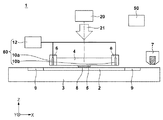
図1は、本発明の一側面としてのインプリント装置1の構成を示す概略図である。インプリント装置1は、物品としての半導体デバイスなどの製造に使用され、モールドを用いて基板上にインプリント材のパターンを形成するリソグラフィ装置である。本実施形態では、インプリント装置1は、基板上に供給されたインプリント材とモールドとを接触させ、インプリント材に硬化用のエネルギーを与えることにより、モールドの凹凸パターンが転写された硬化物のパターンを形成する。
FIG. 1 is a schematic diagram showing a configuration of an
インプリント材には、硬化用のエネルギーが与えられることによって硬化する硬化性組成物(未硬化状態の樹脂と呼ぶこともある)が用いられる。硬化用のエネルギーとしては、電磁波、熱などが用いられる。電磁波としては、例えば、その波長が10nm以上1mm以下の範囲から選択される、赤外線、可視光線、紫外線などの光を用いる。 As the imprint material, a curable composition (also referred to as an uncured resin) that is cured by application of curing energy is used. Electromagnetic waves, heat and the like are used as the curing energy. As the electromagnetic wave, for example, light such as infrared light, visible light, or ultraviolet light whose wavelength is selected from the range of 10 nm or more and 1 mm or less is used.
硬化性組成物は、光の照射によって、或いは、加熱によって硬化する組成物である。光の照射によって硬化する光硬化性組成物は、重合性化合物と光重合開始剤とを少なくとも含有し、必要に応じて、非重合性化合物又は溶剤を含有してもよい。非重合性化合物は、増感剤、水素供与体、内添型離型剤、界面活性剤、酸化防止剤、ポリマー成分などの群から選択される少なくとも一種である。 The curable composition is a composition that is cured by irradiation with light or by heating. The photocurable composition that is cured by irradiation with light contains at least a polymerizable compound and a photopolymerization initiator, and may contain a non-polymerizable compound or a solvent, if necessary. The non-polymerizable compound is at least one selected from the group consisting of a sensitizer, a hydrogen donor, an internal release agent, a surfactant, an antioxidant and a polymer component.
インプリント材は、スピンコーターやスリットコーターによって基板上に膜状に付与されてもよい。また、インプリント材は、液体噴射ヘッドによって、液滴状、或いは、複数の液滴が繋がって形成された島状又は膜状で基板上に付与されてもよい。インプリント材の粘度(25℃における粘度)は、例えば、1mPa・s以上100mPa・s以下である。 The imprint material may be applied in a film form on the substrate by a spin coater or a slit coater. Further, the imprint material may be applied onto the substrate in the form of droplets, or in the form of islands or films formed by connecting a plurality of droplets by the liquid ejecting head. The viscosity of the imprint material (viscosity at 25° C.) is, for example, 1 mPa·s or more and 100 mPa·s or less.
インプリント装置1は、インプリント材の硬化法として光硬化法を採用している。インプリント装置1は、照射部20と、モールド保持部6と、基板ステージ3と、ディスペンサ7と、制御部50とを有する。ここでは、基板上のインプリント材8に紫外線21を照射する照射部20の光軸に平行な方向をZ軸とし、Z軸に垂直な平面内で互いに直交する方向をX軸及びY軸とする。
The
照射部20は、基板上のインプリント材8を硬化させる際に、モールド4を介して、基板上のインプリント材8に紫外線21を照射する。照射部20は、例えば、光源(不図示)と、かかる光源から発せられた紫外線21をインプリント材8の硬化に適した光に調整する光学系とを含む。
The
モールド4は、矩形の外周形状を有し、基板2に対向する面に、基板2に転写すべき凹凸パターン(例えば、回路パターン)が3次元状に形成されたパターン部5を有する。モールド4は、紫外線21を透過させることが可能な材料、例えば、石英で構成されている。
The
モールド保持部6は、モールド4を保持して移動させる。モールド保持部6は、モールド4における紫外線21の照射面の外周領域を真空吸着力や静電力によって引き付けることでモールド4を保持する。モールド保持部6は、モールド4と基板上のインプリント材8との接触(押印)やインプリント材8からのモールド4の引き離し(離型)を選択的に行えるように、モールド4を各軸方向に移動させる。モールド保持部6は、モールド4の高精度な位置決めを実現するために、粗動駆動系や微動駆動系などの複数の駆動系を含んでいてもよい。また、モールド保持部6は、Z軸方向だけではなく、X軸方向、Y軸方向、各軸のθ方向にモールド4を移動させる機能やモールド4の傾きを補正する機能を有していてもよい。
The
インプリント装置1における押印及び離型は、本実施形態のように、モールド4をZ軸方向に移動させることで実現してもよいが、基板2(基板ステージ3)をZ軸方向に移動させることで実現してもよい。また、モールド4と基板2の双方を相対的にZ軸方向に移動させることで、押印及び離型を実現してもよい。
The imprinting and releasing in the
基板2は、ガラス、セラミックス、金属、半導体、樹脂等が用いられ、必要に応じて、その表面に基板とは別の材料からなる部材が形成されていてもよい。基板2としては、具体的に、シリコンウエハ、化合物半導体ウエハ、石英ガラスなどである。基板2には、モールド4のパターン部5で成形されるインプリント材8が供給される。
The
基板ステージ3は、基板2を保持して移動する。基板ステージ3は、モールド4と基板上のインプリント材8とを接触させる際に、モールド4と基板2との位置合わせに用いられる。基板ステージ3は、基板2を各軸方向に移動させる。基板ステージ3は、X軸及びY軸の各方向に対して、粗動駆動系や微動駆動系などの複数の駆動系を含んでいてもよい。また、基板ステージ3は、Z軸方向、各軸のθ方向に基板2を移動させる機能や基板2の傾きを補正する機能を有していてもよい。
The
ディスペンサ7は、モールド保持部6の近傍に配置され、基板2にインプリント材8を供給(吐出)する。インプリント材8は、本実施形態では、紫外線21の照射によって硬化する性質を有するが、その種類は、半導体デバイスの製造工程などの各種条件に応じて適宜選択される。また、ディスペンサ7から吐出されるインプリント材8の量は、基板上に形成すべきインプリント材8の厚さ(残膜厚)や基板上に形成すべきパターンの密度などに応じて適宜決定される。
The
制御部50は、CPUやメモリなどを含み、インプリント装置1の各部を制御してインプリント装置1を動作させる。具体的には、まず、基板2にインプリント材8を供給し、モールド4と基板2とを所定の位置関係に位置決めする。そして、モールド4を−Z方向に移動させて、モールド4(パターン部5)と基板上のインプリント材8とを接触させる。モールド4と基板上のインプリント材8とを接触させた状態でインプリント材8を硬化させ、モールド4を+Z方向に移動させて基板上の硬化したインプリント材8からモールド4を引き離すことで、基板上にインプリント材8のパターンを形成する。
The
ここで、パーティクルなどの異物がモールド4(パターン部5)に付着した状態で、モールド4と基板上のインプリント材8とを接触させると、基板上に形成されるパターンに欠陥が生じたり、モールド4が破損したりする可能性がある。インプリント装置1は、半導体デバイスを製造するための清浄な環境内に配置されているが、異物の発生を完全になくすことは非常に困難である。異物は、インプリント装置1を構成する各部自体から発生したり、インプリント装置1を構成する各部同士の摺動やインプリント装置1の外部からの持ち込みによって発生したりする。
Here, when the
また、インプリント装置1では、一般的に、基板上の硬化したインプリント材8からモールド4を引き離すことによって、モールド4(パターン部5)が帯電する剥離帯電と呼ばれる現象が生じる。このような剥離帯電が生じると、モールド4の周囲の異物がモールド4に引き寄せられ、かかるモールド4に付着する確率が高くなる。モールド4のパターン部5のパターン寸法やパターン深さによって異なるが、ハーフピッチ以上の大きさの異物がモールド4に付着すると、基板上に形成されるパターンの欠陥やモールド4の破損が発生する可能性が高くなる。
Further, in the
このような剥離帯電に対応するために、インプリント装置1においては、モールド4の除電を行う必要がある。従来では、例えば、イオナイザーを用いてモールド4の除電が行われている。イオナイザーには、コロナ放電方式、エネルギー線照射方式(例えば、X線照射方式やα線照射方式)などの多様な種類が存在する。コロナ放電方式は、一般的に、パーティクルの発生要因になる可能性がある。従って、清浄度を維持しながらモールド4を除電するためには、X線照射方式やα線照射方式が好適である。モールド4と基板2との間の空間は非常に狭い空間であるため、かかる空間の周囲にイオナイザーを配置し、モールド4に対して、直接、X線やα線を照射することは困難である。モールド4に対して、直接、X線やα線を照射する方式を除くと、X線やα線を気体に照射して気体をイオン化させ、イオン化された気体をモールド4の下の空間に供給する方式がある。但し、イオン化された気体は、配管及びノズルからモールド4と基板2との間の空間までの経路を通過する間にイオン濃度が低下するため、モールド4の下の空間において十分なイオン濃度を維持することができない場合がある。このような場合には、モールド4を効率的に除電することができなくなる。
In order to deal with such peeling charging, in the
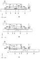
そこで、本実施形態では、モールド4を効率的に除電するために、インプリント装置1は、基板2の周囲を取り囲むように基板ステージ3に配置された補助板9と、モールド4を除電するための気体11を供給する供給部60とを更に有する。但し、補助板9は、基板2の周囲を取り囲んでいなくてもよく、基板ステージ上の基板2が保持される部分の周辺に配置される周辺部材である。また、補助板9は、補助板9の表面の高さと基板2の表面の高さとがほぼ同じ(その差が1mm以下となる)になるように構成されている。供給部60は、気体供給源12と、第1供給部10aと、第2供給部10bとを含む。図2(a)乃至図2(c)に示すように、第1供給部10a及び第2供給部10bは、気体供給源12からの気体11を、モールド4の下の第1空間SP1に隣接する第2空間SP2に供給する。ここで、モールド4の下の第1空間SP1とは、例えば、モールド4と基板2とが対向している場合にはモールド4と基板2との間に規定される空間であり、モールド4と補助板9とが対向している場合にはモールド4と補助板9との間に規定される空間である。第1供給部10aとディスペンサ7とは、モールド保持部6を挟んで配置されている。なお、第1供給部10a、ディスペンサ7、モールド保持部6が一直線上に配置されていなくてもよい。少なくとも、所定方向(本実施形態では、X軸方向)の位置に関して、第1供給部10a、モールド保持部6、ディスペンサ7の順に配置されていれば、Y軸方向の位置が多少ずれていてもよい。また、第2供給部10bは、ディスペンサ7とモールド保持部6との間に配置され、第1供給部10aと第2供給部10bとは、モールド保持部6を挟んで配置されている。
Therefore, in the present embodiment, in order to efficiently eliminate the charge of the
図2(a)乃至図2(b)を参照して、本実施形態におけるモールド4の除電の原理について説明する。図2(a)に示すように、基板2の第1領域(ショット領域)の硬化したインプリント材8からモールド4を引き離すと、モールド4(パターン部5)が帯電する(剥離帯電)。図2(a)には、モールド4がプラス側に帯電する場合を示しているが、モールド4、基板2及びインプリント材8の材質や形状、基板上の硬化したインプリント材8からモールド4を引き離す際の条件などによってモールド4がマイナス側に帯電する場合もある。
The principle of static elimination of the
図2(b)に示すように、基板2の第1領域に硬化したインプリント材8のパターンが形成されたら、基板2の第2領域(ショット領域)にインプリント材8を供給するために、ディスペンサ7の下に基板ステージ3を移動させる必要がある。本実施形態では、基板ステージ3のディスペンサ7の下への移動を開始する前に、第1供給部10aによる気体11の供給を開始する。これにより、基板ステージ3の移動に起因して基板2及び基板ステージ3の表面に発生するクエット流によって、第1供給部10aから第2空間SP2に供給された気体11がモールド4の下の第1空間SP1に引き込まれる。
As shown in FIG. 2B, when the pattern of the cured
図2(c)に示すように、基板ステージ3を移動させてモールド4(パターン部5)と補助板9とを対向させると、モールド4と補助板9との間が第1空間SP1に引き込まれた気体11で満たされているため、かかる気体11を介してモールド4が除電される。
As shown in FIG. 2C, when the
除電用の気体11は、電子に対する平均自由工程が空気よりも長い気体を含む必要がある。気体11としては、具体的には、単原子分子である希ガスがよいが、特に、希ガスのうちでも最も長い平均自由工程を有するヘリウムがよい。電界中に存在する電子は、電界によって陽極側に運ばれ、その途中で気体分子に衝突する。この際、電子が十分に加速されて気体の電離電圧以上のエネルギーを有して気体分子に衝突すると電離が起こり、電子−陽イオン対が生成される。ここで生成された電子も電界で加速され、気体分子を電離させる。このように、電離が次々に起こることで大量の電子−陽イオン対が生成される現象を電子雪崩と呼ぶ。電子に対する平均自由工程が長い気体は、加速中の電子が途中で気体分子に衝突せず、高エネルギー状態まで加速される。従って、電子に対する平均自由工程が長い気体は、空気と比べて、低い電界中でも電子雪崩が起こりやすく、モールド4に大きな電圧が蓄積される前に除電することができる。
The
また、モールド4と対向する補助板9は、モールド4の側の面に導電性を有している。補助板9は、本実施形態では、金属で構成されている。これにより、気体中で電離したイオンが電界で加速され補助板9(のモールド4の側の面)に衝突した際に2次電子を放出し、かかる2次電子が更に電子雪崩に関与するため、モールド4の除電効率を向上させることができる。
Further, the
図3を参照して、インプリント装置1におけるインプリント処理について、特に、モールド4の除電に注目して説明する。かかるインプリント処理は、制御部50がインプリント装置1の各部を統括的に制御することで行われる。ここでは、基板2のショット領域としての第1領域及び第2領域のそれぞれに、インプリント材8のパターンを順に形成する場合を例に説明する。
With reference to FIG. 3, the imprint process in the
S302では、基板2を保持した基板ステージ3を移動させて基板2の第1領域をディスペンサ7の下に位置決めし、ディスペンサ7から基板2の第1領域にインプリント材8を供給する。この際、供給部60(第1供給部10a及び第2供給部10b)による気体11の供給を停止させている。
In S302, the
S304では、基板ステージ3のモールド4の下への移動を開始する前に、供給部60、具体的には、第2供給部10bによる気体11の供給を開始する。なお、本実施形態では、気体11の使用量を抑えるために、第2供給部10bのみから気体11を供給しているが、気体11の使用量を抑える必要がなければ、第2供給部10bに加えて第1供給部10aからも気体11を供給してもよい。
In S304, the supply of the
S306では、基板ステージ3を移動させて基板2の第1領域をモールド4の下に位置決めする。この際、第2供給部10bによる気体11の供給を継続させている。これにより、第2供給部10bから第2空間SP2に供給された気体11がモールド4の下の第1空間SP1に引き込まれ、モールド4と基板2(基板2の第1領域のインプリント材8)との間を気体11で満たすことができる。
In S306, the
S308では、モールド4と基板2の第1領域のインプリント材8とを接触させる。モールド4とインプリント材8とを接触させてインプリント材8をモールド4のパターン部5に充填している間、第2供給部10bによる気体11の供給を継続させて、モールド4の下の第1空間SP1における気体11の濃度が99%以上になるようにする。これにより、モールド4のパターン部5へのインプリント材8の充填を促進させることができる。
In S308, the
S310では、モールド4とインプリント材8とを接触させた状態で基板2の第1領域のインプリント材8を硬化させる前に、第2供給部10bによる気体11の供給を停止する。ここでは、モールド4の下の第1空間SP1における気体11の濃度が99%未満、更に詳細には、90%以下になるようにする。つまり、S308の工程のときよりも、モールド4の周囲の酸素の割合が増えるようにする。モールド4と基板上のインプリント材8とを接触させると、インプリント材8の一部がモールド4のパターン部5からはみ出してパターン部5の側面(へり)に付着することがある。このようにパターン部5の側面に付着したインプリント材8が硬化すると、かかる硬化したインプリント材8が剥がれ落ちてパーティクルとなる。従って、パターン部5の側面に付着したインプリント材8は、硬化させない、即ち、未硬化の状態のままにしておく方がよい。そこで、本実施形態では、モールド4の下の第1空間SP1における気体11の濃度を上げて、紫外線21によるインプリント材8の硬化反応を酸素で阻害させている。なお、パターン部5の側面に付着した未硬化のインプリント材8は微量であるので、第2領域に供給されたインプリント材8を硬化させるときまでには揮発する。従って、第2領域におけるパターン形成への影響はない。
In S310, the supply of the
S312では、モールド4と基板2の第1領域のインプリント材8とを接触させた状態において、照射部20からインプリント材8に紫外線21を照射してインプリント材8を硬化させる。この際、供給部60(第2供給部10b)による気体11の供給は停止させたままにする。
In S312, in a state where the
S314では、基板2の第1領域の硬化したインプリント材8からモールド4を引き離す前に、供給部60、具体的には、第1供給部10aによる気体11の供給を開始する。なお、本実施形態では、気体11の使用量を抑えるために、第1供給部10aのみから気体11を供給しているが、気体11の使用量を抑える必要がなければ、第1供給部10aに加えて第2供給部10bからも気体11を供給してもよい。
In S314, before the
S316では、基板2の第1領域の硬化したインプリント材8からモールド4を引き離す。これにより、基板2の第1領域にインプリント材8のパターンが形成される。一方、基板2の第1領域の硬化したインプリント材8からモールド4を引き離すことによって、モールド4(パターン部5)が帯電する。この際、第1供給部10aによる気体11の供給を継続させている。
In S316, the
S317では、基板2の全てのショット領域にインプリント材8のパターンを形成したかどうかを判定する。基板2の全てのショット領域にインプリント材8のパターンを形成している場合には、第1供給部10aによる気体11の供給を停止して動作を終了する。基板2の全てのショット領域にインプリント材8のパターンを形成していない場合には、S318に移行する。
In S317, it is determined whether or not the pattern of the
S318では、基板2の第1領域とは異なる第2領域にインプリント材8を供給するために、基板ステージ3のディスペンサ7の下への移動を開始する。この際、第1供給部10aによる気体11の供給を継続させている。換言すれば、基板ステージ3のディスペンサ7の下への移動を行っている間、第1供給部10aによる気体11の供給を継続する。このように、基板ステージ3のディスペンサ7の下への移動を開始する前に第1供給部10aによる気体11の供給を開始しているため、第1供給部10aから第2空間SP2に供給された気体11がモールド4の下の第1空間SP1に引き込まれる。従って、モールド4の下の第1空間SP1が気体11で満たされ、基板ステージ3が移動することによって、補助板9とモールド4とが対向したときに、電子雪崩によって電子−陽イオン対が生成される。そして、電子−陽イオン対がモールド4に近づくことでモールド4が除電される。このように、モールド4の下の第1空間SP1に送られた気体11を介してモールド4が除電される。また、モールド4の除電を行うときのモールド4と補助板9との間の空間における気体11の濃度が99%以上となるように、第1供給部10aによる気体11の供給が制御されている。なお、本実施形態では、基板ステージ3をディスペンサ7の下に移動させている間においてモールド4の除電が完了することを想定している。但し、モールド4の除電が完了しない場合には、補助板9とモールド4とが対向した状態において基板ステージ3を停止させてもよいし、補助板9とモールド4とが対向した状態での基板ステージ3の速度を遅くしてもよい。
In S318, in order to supply the
S320では、基板2の第2領域をディスペンサの下に位置決めする。この際、第1供給部10aによる気体11の供給を停止する。換言すれば、基板ステージ3がディスペンサ7の下に到達したら第1供給部10aによる気体11の供給を停止する。そして、S302に移行して、基板2の第2領域にインプリント材8を供給し、基板2の第2領域にインプリント材8のパターンを形成するための処理を続ける。
In S320, the second region of the
このように、基板2の第1領域の硬化したインプリント材8からモールド4を引き離した後、基板2の第2領域にインプリント材8を供給するための基板ステージ3のディスペンサ7の下への移動を開始する前に第1供給部10aによる気体11の供給を開始する。そして、基板ステージ3をディスペンサ7の下に移動させることで第2空間SP2に供給された気体11を第1空間SP1に送り、補助板9をモールド4に対向させることにより気体11を介してモールド4の除電を行う。従って、本実施形態におけるインプリント装置1では、モールド4を効率的に除電することができるため、モールド4への異物の付着を抑制して、基板上に形成されるパターンの欠陥の発生やモールド4の破損を低減することができる。
In this way, after the
なお、本実施形態では、基板上の硬化したインプリント材8からモールド4を引き離す際に、第1供給部10aから気体11を供給しているが、これに限定されるものではない。例えば、基板上の硬化したインプリント材8からモールド4を引き離す前には、第1供給部10aからの気体11の供給を開始せず、基板上の硬化したインプリント材8からモールド4を引き離した後で、第1供給部10aからの気体11の供給を開始してもよい。
In the present embodiment, the
また、図4に示すように、補助板9は、電気的に接地されていてもよい。これにより、モールド4(パターン部5)と補助板9との間で電子雪崩によるモールド4の除電が行われる際に、モールド4の電位が接地された補助板9の電位と同じになる。従って、モールド4の電位がインプリント装置1の内部の部材と等電位になるため、モールド4の周辺で強い電界が発生せず、静電気力による異物の付着を抑制することができる。
Further, as shown in FIG. 4, the
また、インプリント装置1は、図5に示すように、補助板9に電位を与える付与部70を更に有していてもよい。そして、補助板9をモールド4に対向させるときに、付与部70により、補助板9に、基板上の硬化したインプリント材8からモールド4を引き離すことによってモールド4に生じる電位の極性とは逆の極性の電位を与える。これにより、モールド4と補助板9との間の電位差が広がり、モールド4と補助板9との間の電界が強くなるため、電子雪崩が起こりやすくなる。従って、剥離帯電によるモールド4の帯電量が少ない場合であっても、電子雪崩によるモールド4の除電を行うことができる。図5に示すように、モールド4がプラス側に帯電している場合には、付与部70により、マイナスの電位を補助板9に与えればよい。一方、モールド4がマイナス側に帯電している場合には、付与部70により、プラスの電位を補助板9に与えればよい。付与部70は、両極の電位を補助板9に与えられるような電源を含む。
Moreover, the
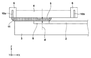
また、モールド4と補助板9との間で起こる電子雪崩は、気体11の種類だけではなく、モールド4と補助板9との間の距離を調整することで制御することが可能である。例えば、モールド4と補助板9との間の距離を調整することで、モールド4と補助板9との間の電界強度を調整することができる。そこで、図6に示すように、補助板9をモールド4に対向させるときに、モールド4と補助板9との間の距離dを調整する。モールド4と補助板9との間の距離dを変更する距離変更部としては、モールド保持部6や基板ステージ3を用いることができる。
The electronic avalanche that occurs between the
また、モールド4と補助板9との間で起こる電子雪崩は、モールド4と補助板9との間の空間の圧力を調整することで制御することが可能である。例えば、モールド4と補助板9との間の空間の圧力を調整することで、モールド4と補助板9との間の電子の平均自由工程を調整することができる。
そこで、モールド4と補助板9との間の空間の圧力を変更する圧力変更部を設けて、補助板9をモールド4に対向させるときに、圧力変更部により、モールド4と補助板9との間の空間の圧力を調整する。圧力変更部は、モールド4と補助板9との間の空間の圧力、或いは、かかる空間を含む近傍の圧力を局所的に変更してもよいし、インプリント装置1の全体の空間の圧力を変更してもよい。
The electronic avalanche that occurs between the
Therefore, when a pressure changing unit that changes the pressure in the space between the
また、図7に示すように、インプリント装置1は、補助板9に光31を照射するエネルギー照射部30を更に有していてもよい。そして、補助板9をモールド4に対向させるときに、エネルギー照射部30により、補助板9に、補助板9の仕事関数以上のエネルギーを有する光31を照射する。例えば、補助板9がアルミニウムで構成されている場合、補助板9の仕事関数は約4eVであるため、波長300nm以下の光31を照射すれば、光電効果により補助板9(のモールド4の側の面)から光電子が放出される。金属の仕事関数は、一般的に、2eV〜5eV程度であるため、紫外線領域の光31を補助板9に照射することで、光電効果により補助板9から光電子が放出される。かかる光電子は、電子雪崩に関与するため、モールド4の除電効率を更に向上させることができる。
Further, as shown in FIG. 7, the
また、インプリント装置1で使用する除電用の気体11は、一般的に、拡散性が高い。従って、上述したように、モールド4と基板上のインプリント材8とを接触させる際に、モールド4と基板2との間の空間を気体11で満たすことで、モールド4のパターン部5に対するインプリント材8の充填性を向上させることができる。このため、モールド4と基板上のインプリント材8とを接触させる工程の間は、気体11を供給するとよい。但し、気体11として用いられる希ガスは高価であるため、モールド4のパターン部5へのインプリント材8の充填が完了し、インプリント材8を硬化させる工程の間は、気体11の供給を停止するとよい。
The
インプリント装置1を用いて形成した硬化物のパターンは、各種物品の少なくとも一部に恒久的に、或いは、各種物品を製造する際に一時的に、用いられる。物品とは、電気回路素子、光学素子、MEMS、記録素子、センサー、或いは、型などである。電気回路素子としては、DRAM、SRAM、フラッシュメモリ、MRAMなどの揮発性又は不揮発性の半導体メモリや、LSI、CCD、イメージセンサ、FPGAなどの半導体素子などが挙げられる。型としては、インプリント用のモールドなどが挙げられる。
The pattern of the cured product formed by using the
硬化物のパターンは、上述の物品の少なくとも一部の構成部材として、そのまま用いられるか、或いは、マスクとして一時的に用いられる。基板の加工工程においてエッチング又はイオン注入などが行われた後、マスクは除去される。 The pattern of the cured product is used as it is as a constituent member of at least a part of the above-mentioned article, or is temporarily used as a mask. After etching or ion implantation is performed in the substrate processing step, the mask is removed.
次に、物品の具体的な製造方法について説明する。図8(a)に示すように、絶縁体などの被加工材が表面に形成されたシリコンウエハなどの基板2を用意し、続いて、インクジェット法などにより、被加工材の表面にインプリント材8を付与する。ここでは、複数の液滴状になったインプリント材8が基板上に付与された様子を示している。
Next, a specific method for manufacturing the article will be described. As shown in FIG. 8A, a
図8(b)に示すように、インプリント用のモールド4を、その凹凸パターンが形成された側を基板上のインプリント材8に向け、対向させる。図8(c)に示すように、インプリント材8が付与された基板2とモールド4とを接触させ、圧力を加える。インプリント材8は、モールド4と被加工材との隙間に充填される。この状態で硬化用のエネルギーとして光をモールド4を介して照射すると、インプリント材8は硬化する。
As shown in FIG. 8B, the
図8(d)に示すように、インプリント材8を硬化させた後、モールド4と基板2を引き離すと、基板上にインプリント材8の硬化物のパターンが形成される。この硬化物のパターンは、モールド4の凹部が硬化物の凸部に、モールド4の凸部が硬化物の凹部に対応した形状になっており、即ち、インプリント材8にモールド4の凹凸パターンが転写されたことになる。
As shown in FIG. 8D, when the
図8(e)に示すように、硬化物のパターンを耐エッチングマスクとしてエッチングを行うと、被加工材の表面のうち、硬化物がない、或いは、薄く残存した部分が除去され、溝となる。図8(f)に示すように、硬化物のパターンを除去すると、被加工材の表面に溝が形成された物品を得ることができる。ここでは、硬化物のパターンを除去したが、加工後も除去せずに、例えば、半導体素子などに含まれる層間絶縁用の膜、即ち、物品の構成部材として利用してもよい。 As shown in FIG. 8E, when etching is performed using the pattern of the cured product as an etching-resistant mask, the portion of the surface of the material to be processed where the cured product is absent or remains thin is removed to form a groove. .. As shown in FIG. 8(f), by removing the pattern of the cured product, an article having grooves formed on the surface of the material to be processed can be obtained. Although the pattern of the cured product is removed here, it may be used as a film for interlayer insulation contained in a semiconductor element or the like, that is, as a constituent member of an article without being removed even after processing.
以上、本発明の好ましい実施形態について説明したが、本発明はこれらの実施形態に限定されないことはいうまでもなく、その要旨の範囲内で種々の変形及び変更が可能である。 Although the preferred embodiments of the present invention have been described above, it goes without saying that the present invention is not limited to these embodiments, and various modifications and changes can be made within the scope of the gist thereof.
1:インプリント装置 2:基板 3:基板ステージ 4:モールド 6:モールド保持部 7:ディスペンサ 9:補助板 50:制御部 60:供給部 1: Imprinting device 2: Substrate 3: Substrate stage 4: Mold 6: Mold holding unit 7: Dispenser 9: Auxiliary plate 50: Control unit 60: Supply unit
Claims (16)
前記基板を保持して移動するステージと、
前記ステージ上の前記基板が保持される部分の周辺に配置され、前記モールドの側の面に導電性を有する周辺部材と、
前記モールドの下の第1空間に隣接する第2空間に気体を供給する第1供給部と、
前記基板にインプリント材を供給するディスペンサと、
前記ステージの移動及び前記第1供給部を制御する制御部と、を有し、
前記第1供給部と前記ディスペンサとは、前記モールドを保持する保持部を挟んで配置され、
前記制御部は、前記基板の第1領域の硬化したインプリント材と前記モールドとを引き離した後、前記基板の前記第1領域とは異なる第2領域にインプリント材を供給するための前記ステージの前記ディスペンサの下への移動を開始する前に前記第1供給部による前記気体の供給を開始し、前記ステージを前記ディスペンサの下に向けて移動させることで前記第2空間に供給された前記気体を前記第1空間に送り、前記周辺部材を前記モールドに対向させることにより前記気体を介して前記モールドの除電を行うことを特徴とするインプリント装置。 An imprint apparatus that forms a pattern on the substrate by curing the imprint material in a state where the mold and the imprint material on the substrate are in contact with each other,
A stage for holding and moving the substrate,
A peripheral member that is arranged around the portion on the stage where the substrate is held, and has a conductive peripheral surface on the mold side,
A first supply unit for supplying gas to a second space below the mold and adjacent to the first space;
A dispenser for supplying an imprint material to the substrate,
A control unit that controls the movement of the stage and the first supply unit,
The first supply unit and the dispenser are arranged with a holding unit holding the mold interposed therebetween,
The controller separates the cured imprint material in the first region of the substrate from the mold, and then supplies the imprint material to a second region of the substrate different from the first region. Of the gas supplied to the second space by starting the supply of the gas by the first supply unit before starting the movement of the stage below the dispenser, and moving the stage toward the bottom of the dispenser. An imprint apparatus, wherein a gas is sent to the first space, and the peripheral member is opposed to the mold to perform static elimination of the mold through the gas.
前記第1供給部と前記第2供給部とは、前記保持部を挟んで配置され、
前記制御部は、前記ステージが前記ディスペンサの下に到達したら前記第1供給部による前記気体の供給を停止し、前記第2領域にインプリント材を供給した後、前記ステージの前記モールドの下への移動を開始する前に前記第2供給部による前記気体の供給を開始し、前記ステージを前記モールドの下に移動させることで前記第2空間に供給された前記気体を前記第1空間に送ることを特徴とする請求項1乃至3のうちいずれか1項に記載のインプリント装置。 Further comprising a second supply unit arranged between the dispenser and the holding unit, for supplying the gas to the second space,
The first supply unit and the second supply unit are arranged with the holding unit interposed therebetween,
When the stage reaches below the dispenser, the control unit stops the supply of the gas by the first supply unit, supplies the imprint material to the second region, and then moves to the bottom of the mold of the stage. Of the gas supplied from the second supply unit before the movement of the gas is started, and the gas supplied to the second space is sent to the first space by moving the stage below the mold. The imprint apparatus according to claim 1, wherein the imprint apparatus is an imprint apparatus.
前記制御部は、前記周辺部材を前記モールドに対向させるときに、前記付与部により、前記周辺部材に、前記基板上の硬化したインプリント材と前記モールドとを引き離すことによって前記モールドに生じる電位の極性とは逆の極性の電位を与えることを特徴とする請求項1乃至7のうちいずれか1項に記載のインプリント装置。 Further having an applying portion for applying an electric potential to the peripheral member,
When the peripheral section faces the mold, the control section controls the potential applied to the mold by separating the cured imprint material on the substrate from the mold by the applying section by the applying section. The imprint apparatus according to claim 1, wherein a potential having a polarity opposite to that of the polarity is applied.
前記制御部は、前記周辺部材を前記モールドに対向させるときに、前記距離変更部により、前記モールドと前記周辺部材との間の距離を調整することを特徴とする請求項1乃至9のうちいずれか1項に記載のインプリント装置。 Further comprising a distance changing unit for changing the distance between the mold and the peripheral member,
The control unit adjusts the distance between the mold and the peripheral member by the distance changing unit when the peripheral member faces the mold. The imprint apparatus according to Item 1.
前記制御部は、前記周辺部材を前記モールドに対向させるときに、前記圧力変更部により、前記モールドと前記周辺部材との間の空間の圧力を調整することを特徴とする請求項1乃至10のうちいずれか1項に記載のインプリント装置。 Further comprising a pressure changing portion for changing the pressure of the space between the mold and the peripheral member,
The control unit adjusts the pressure of the space between the mold and the peripheral member by the pressure changing unit when the peripheral member is opposed to the mold. The imprint apparatus according to any one of the above.
前記制御部は、前記周辺部材を前記モールドに対向させるときに、前記照射部により、前記周辺部材に、前記周辺部材の仕事関数以上のエネルギーを有する光を照射することを特徴とする請求項1乃至11のうちいずれか1項に記載のインプリント装置。 Further having an irradiation unit for irradiating the peripheral member with light,
The control unit irradiates the peripheral member with light having an energy equal to or higher than a work function of the peripheral member by the irradiation unit when the peripheral member faces the mold. 12. The imprint apparatus according to any one of 1 to 11 .
前記インプリント装置は、前記基板を保持して移動するステージと、前記ステージ上の前記基板が保持される部分の周辺に配置され、前記モールドの側の面に導電性を有する周辺部材と、前記モールドの下の第1空間に隣接する第2空間に気体を供給する第1供給部と、前記基板にインプリント材を供給するディスペンサと、を有し、
前記第1供給部と前記ディスペンサとは、前記モールドを保持する保持部を挟んで配置され、
前記インプリント方法は、前記基板の第1領域の硬化したインプリント材と前記モールドとを引き離した後、前記基板の前記第1領域とは異なる第2領域にインプリント材を供給するための前記ステージの前記ディスペンサの下への移動を開始する前に前記第1供給部による前記気体の供給を開始し、前記ステージを前記ディスペンサの下に向けて移動させることで前記第2空間に供給された前記気体を前記第1空間に送り、前記周辺部材を前記モールドに対向させることにより前記気体を介して前記モールドの除電を行う工程を有することを特徴とするインプリント方法。 An imprint method using an imprint apparatus that forms a pattern on the substrate by curing the imprint material in a state where the mold and the imprint material on the substrate are in contact with each other,
The imprint apparatus includes a stage that holds and moves the substrate, a peripheral member that is arranged around a portion of the stage where the substrate is held, and has a conductive surface on a side of the mold, A first supply unit that supplies a gas to a second space adjacent to the first space under the mold; and a dispenser that supplies an imprint material to the substrate,
The first supply unit and the dispenser are arranged with a holding unit holding the mold interposed therebetween,
In the imprint method, after separating the cured imprint material in the first region of the substrate from the mold, the imprint material is supplied to a second region of the substrate different from the first region. The gas is supplied to the second space by starting the supply of the gas by the first supply unit before starting the movement of the stage below the dispenser and moving the stage toward the bottom of the dispenser. An imprinting method, comprising the step of discharging the gas through the gas by sending the gas to the first space and causing the peripheral member to face the mold.
前記工程で前記パターンが形成された前記基板を処理する工程と、
を有することを特徴とする物品の製造方法。 Forming a pattern on a substrate using the imprint apparatus according to any one of claims 1 to 14,
A step of processing the substrate on which the pattern is formed in the step,
A method for manufacturing an article, comprising:
Priority Applications (5)
| Application Number | Priority Date | Filing Date | Title |
|---|---|---|---|
| JP2016225375A JP6735656B2 (en) | 2016-11-18 | 2016-11-18 | Imprint apparatus, imprint method, and article manufacturing method |
| PCT/JP2017/036246 WO2018092454A1 (en) | 2016-11-18 | 2017-10-05 | Imprint device, imprint method, and article manufacturing method |
| KR1020197016503A KR102179737B1 (en) | 2016-11-18 | 2017-10-05 | Imprint apparatus, imprint method, and article manufacturing method |
| TW106135607A TWI661925B (en) | 2016-11-18 | 2017-10-18 | Imprinting device, imprinting method, and article manufacturing method |
| US16/408,586 US11333971B2 (en) | 2016-11-18 | 2019-05-10 | Imprint apparatus, imprint method, and method of manufacturing article |
Applications Claiming Priority (1)
| Application Number | Priority Date | Filing Date | Title |
|---|---|---|---|
| JP2016225375A JP6735656B2 (en) | 2016-11-18 | 2016-11-18 | Imprint apparatus, imprint method, and article manufacturing method |
Publications (3)
| Publication Number | Publication Date |
|---|---|
| JP2018082127A JP2018082127A (en) | 2018-05-24 |
| JP2018082127A5 JP2018082127A5 (en) | 2019-12-19 |
| JP6735656B2 true JP6735656B2 (en) | 2020-08-05 |
Family
ID=62146147
Family Applications (1)
| Application Number | Title | Priority Date | Filing Date |
|---|---|---|---|
| JP2016225375A Active JP6735656B2 (en) | 2016-11-18 | 2016-11-18 | Imprint apparatus, imprint method, and article manufacturing method |
Country Status (5)
| Country | Link |
|---|---|
| US (1) | US11333971B2 (en) |
| JP (1) | JP6735656B2 (en) |
| KR (1) | KR102179737B1 (en) |
| TW (1) | TWI661925B (en) |
| WO (1) | WO2018092454A1 (en) |
Families Citing this family (2)
| Publication number | Priority date | Publication date | Assignee | Title |
|---|---|---|---|---|
| JP7149872B2 (en) * | 2019-02-14 | 2022-10-07 | キヤノン株式会社 | IMPRINT METHOD, IMPRINT APPARATUS, AND ARTICLE MANUFACTURING METHOD |
| US11181819B2 (en) | 2019-05-31 | 2021-11-23 | Canon Kabushiki Kaisha | Frame curing method for extrusion control |
Family Cites Families (14)
| Publication number | Priority date | Publication date | Assignee | Title |
|---|---|---|---|---|
| FR2133154A5 (en) | 1971-04-09 | 1972-11-24 | Cii | |
| JP2007098779A (en) | 2005-10-05 | 2007-04-19 | Nikon Corp | Peeling method of resin and pattern transfer apparatus |
| JP5137635B2 (en) * | 2007-03-16 | 2013-02-06 | キヤノン株式会社 | Imprint method, chip manufacturing method, and imprint apparatus |
| JP5235506B2 (en) * | 2008-06-02 | 2013-07-10 | キヤノン株式会社 | Pattern transfer apparatus and device manufacturing method |
| JP5868215B2 (en) * | 2012-02-27 | 2016-02-24 | キヤノン株式会社 | Imprint apparatus, imprint method, and article manufacturing method using the same |
| JP6123396B2 (en) * | 2013-03-18 | 2017-05-10 | 大日本印刷株式会社 | Imprint method and imprint apparatus |
| JP5865340B2 (en) * | 2013-12-10 | 2016-02-17 | キヤノン株式会社 | Imprint apparatus and article manufacturing method |
| JP2016031952A (en) * | 2014-07-25 | 2016-03-07 | キヤノン株式会社 | Imprint device and method of manufacturing article |
| JP6661397B2 (en) * | 2015-04-22 | 2020-03-11 | キヤノン株式会社 | Imprint apparatus, imprint method, and article manufacturing method |
| JP6603678B2 (en) * | 2016-02-26 | 2019-11-06 | キヤノン株式会社 | Imprint apparatus, operation method thereof, and article manufacturing method |
| JP6643145B2 (en) * | 2016-02-29 | 2020-02-12 | キヤノン株式会社 | Imprint apparatus, mold, imprint method, and article manufacturing method |
| JP6732475B2 (en) * | 2016-02-29 | 2020-07-29 | キヤノン株式会社 | Imprint apparatus, article manufacturing method, holding apparatus, and exposure apparatus |
| JP6704769B2 (en) * | 2016-03-29 | 2020-06-03 | キヤノン株式会社 | Imprint apparatus and article manufacturing method |
| US10754244B2 (en) * | 2016-03-31 | 2020-08-25 | Canon Kabushiki Kaisha | Pattern forming method as well as production methods for processed substrate, optical component, circuit board, electronic component and imprint mold |
-
2016
- 2016-11-18 JP JP2016225375A patent/JP6735656B2/en active Active
-
2017
- 2017-10-05 KR KR1020197016503A patent/KR102179737B1/en active IP Right Grant
- 2017-10-05 WO PCT/JP2017/036246 patent/WO2018092454A1/en active Application Filing
- 2017-10-18 TW TW106135607A patent/TWI661925B/en active
-
2019
- 2019-05-10 US US16/408,586 patent/US11333971B2/en active Active
Also Published As
| Publication number | Publication date |
|---|---|
| WO2018092454A1 (en) | 2018-05-24 |
| US20190265589A1 (en) | 2019-08-29 |
| JP2018082127A (en) | 2018-05-24 |
| TW201819153A (en) | 2018-06-01 |
| TWI661925B (en) | 2019-06-11 |
| KR20190073573A (en) | 2019-06-26 |
| KR102179737B1 (en) | 2020-11-17 |
| US11333971B2 (en) | 2022-05-17 |
Similar Documents
| Publication | Publication Date | Title |
|---|---|---|
| US11333971B2 (en) | Imprint apparatus, imprint method, and method of manufacturing article | |
| JP7261000B2 (en) | CONTAINER, PROCESSING APPARATUS, CONTENT REMOVAL METHOD, AND PRODUCT MANUFACTURING METHOD | |
| US10777443B2 (en) | Imprint apparatus, imprinting method, and method for manufacturing article | |
| WO2016170729A1 (en) | Imprint apparatus, method of imprinting, and method of manufacturing article | |
| TW201724677A (en) | System and method for discharging electrostatic charge in nanoimprint lithography processes | |
| TWI618116B (en) | Imprinting device and method of manufacturing the same | |
| JP6704769B2 (en) | Imprint apparatus and article manufacturing method | |
| JP6603678B2 (en) | Imprint apparatus, operation method thereof, and article manufacturing method | |
| TWI680050B (en) | Imprint device, operation method thereof, and article manufacturing method | |
| JP2020013890A (en) | Imprint device, control method thereof, and article manufacturing method | |
| JP2019091741A (en) | Imprint apparatus, imprint method, and article manufacturing method | |
| KR102294037B1 (en) | Imprint apparatus, and method of manufacturing article | |
| JP2019067916A (en) | Lithography apparatus and method of manufacturing article | |
| JP6732475B2 (en) | Imprint apparatus, article manufacturing method, holding apparatus, and exposure apparatus | |
| WO2017134989A1 (en) | Imprinting device, and article production method | |
| JP7118674B2 (en) | Molding apparatus for molding composition on substrate using mold, molding method, and article manufacturing method | |
| US20230347390A1 (en) | Foreign particle removing method, formation method, article manufacturing method, foreign particle removing apparatus, and system | |
| JP2019041004A (en) | Imprint apparatus and method of manufacturing article | |
| JP6921690B2 (en) | Dust collectors, substrate processing systems, and article manufacturing methods | |
| US10303049B2 (en) | Reducing electric charge in imprint lithography | |
| JP2019117845A (en) | Lithographic apparatus and article manufacturing method | |
| JP2018190802A (en) | Imprint device and method of manufacturing article | |
| JP2019096696A (en) | Imprint apparatus, imprint method, and article manufacturing method |
Legal Events
| Date | Code | Title | Description |
|---|---|---|---|
| A521 | Request for written amendment filed |
Free format text: JAPANESE INTERMEDIATE CODE: A523 Effective date: 20191107 |
|
| A621 | Written request for application examination |
Free format text: JAPANESE INTERMEDIATE CODE: A621 Effective date: 20191107 |
|
| TRDD | Decision of grant or rejection written | ||
| A01 | Written decision to grant a patent or to grant a registration (utility model) |
Free format text: JAPANESE INTERMEDIATE CODE: A01 Effective date: 20200615 |
|
| A61 | First payment of annual fees (during grant procedure) |
Free format text: JAPANESE INTERMEDIATE CODE: A61 Effective date: 20200714 |
|
| R151 | Written notification of patent or utility model registration |
Ref document number: 6735656 Country of ref document: JP Free format text: JAPANESE INTERMEDIATE CODE: R151 |