JP6726834B2 - Method for forming an etching mask for sub-resolution substrate patterning - Google Patents
Method for forming an etching mask for sub-resolution substrate patterning Download PDFInfo
- Publication number
- JP6726834B2 JP6726834B2 JP2018515551A JP2018515551A JP6726834B2 JP 6726834 B2 JP6726834 B2 JP 6726834B2 JP 2018515551 A JP2018515551 A JP 2018515551A JP 2018515551 A JP2018515551 A JP 2018515551A JP 6726834 B2 JP6726834 B2 JP 6726834B2
- Authority
- JP
- Japan
- Prior art keywords
- mandrel
- forming
- sidewall
- materials
- etching
- Prior art date
- Legal status (The legal status is an assumption and is not a legal conclusion. Google has not performed a legal analysis and makes no representation as to the accuracy of the status listed.)
- Active
Links
- 239000000758 substrate Substances 0.000 title claims description 87
- 238000000034 method Methods 0.000 title claims description 75
- 238000005530 etching Methods 0.000 title claims description 70
- 238000000059 patterning Methods 0.000 title claims description 29
- 239000000463 material Substances 0.000 claims description 287
- 125000006850 spacer group Chemical group 0.000 claims description 105
- 238000000151 deposition Methods 0.000 claims description 17
- 238000000206 photolithography Methods 0.000 claims description 10
- 239000004065 semiconductor Substances 0.000 claims description 7
- 230000008021 deposition Effects 0.000 claims description 6
- 230000003287 optical effect Effects 0.000 claims description 5
- 239000000126 substance Substances 0.000 claims description 4
- 238000005498 polishing Methods 0.000 claims description 2
- 238000007517 polishing process Methods 0.000 claims description 2
- 239000011295 pitch Substances 0.000 description 38
- 230000005855 radiation Effects 0.000 description 7
- 238000000231 atomic layer deposition Methods 0.000 description 6
- 230000008901 benefit Effects 0.000 description 5
- 230000015572 biosynthetic process Effects 0.000 description 5
- 238000005516 engineering process Methods 0.000 description 4
- 229920002120 photoresistant polymer Polymers 0.000 description 4
- 238000005520 cutting process Methods 0.000 description 3
- 239000010408 film Substances 0.000 description 3
- 238000003860 storage Methods 0.000 description 3
- 238000003491 array Methods 0.000 description 2
- 230000009286 beneficial effect Effects 0.000 description 2
- 239000002131 composite material Substances 0.000 description 2
- 239000007789 gas Substances 0.000 description 2
- 238000004519 manufacturing process Methods 0.000 description 2
- 150000004767 nitrides Chemical class 0.000 description 2
- XUIMIQQOPSSXEZ-UHFFFAOYSA-N Silicon Chemical compound [Si] XUIMIQQOPSSXEZ-UHFFFAOYSA-N 0.000 description 1
- 238000010420 art technique Methods 0.000 description 1
- 239000003086 colorant Substances 0.000 description 1
- 230000001419 dependent effect Effects 0.000 description 1
- 238000010586 diagram Methods 0.000 description 1
- 238000007654 immersion Methods 0.000 description 1
- 238000000671 immersion lithography Methods 0.000 description 1
- 230000000873 masking effect Effects 0.000 description 1
- 239000011159 matrix material Substances 0.000 description 1
- 229910052751 metal Inorganic materials 0.000 description 1
- 239000002184 metal Substances 0.000 description 1
- 150000002739 metals Chemical class 0.000 description 1
- 238000003672 processing method Methods 0.000 description 1
- 230000002040 relaxant effect Effects 0.000 description 1
- 230000003252 repetitive effect Effects 0.000 description 1
- 230000000717 retained effect Effects 0.000 description 1
- 229910052710 silicon Inorganic materials 0.000 description 1
- 239000010703 silicon Substances 0.000 description 1
- 238000004513 sizing Methods 0.000 description 1
- 239000002904 solvent Substances 0.000 description 1
- 239000010409 thin film Substances 0.000 description 1
- XLYOFNOQVPJJNP-UHFFFAOYSA-N water Substances O XLYOFNOQVPJJNP-UHFFFAOYSA-N 0.000 description 1
Images


Classifications
-
- H—ELECTRICITY
- H01—ELECTRIC ELEMENTS
- H01L—SEMICONDUCTOR DEVICES NOT COVERED BY CLASS H10
- H01L21/00—Processes or apparatus adapted for the manufacture or treatment of semiconductor or solid state devices or of parts thereof
- H01L21/02—Manufacture or treatment of semiconductor devices or of parts thereof
- H01L21/027—Making masks on semiconductor bodies for further photolithographic processing not provided for in group H01L21/18 or H01L21/34
- H01L21/033—Making masks on semiconductor bodies for further photolithographic processing not provided for in group H01L21/18 or H01L21/34 comprising inorganic layers
- H01L21/0334—Making masks on semiconductor bodies for further photolithographic processing not provided for in group H01L21/18 or H01L21/34 comprising inorganic layers characterised by their size, orientation, disposition, behaviour, shape, in horizontal or vertical plane
- H01L21/0337—Making masks on semiconductor bodies for further photolithographic processing not provided for in group H01L21/18 or H01L21/34 comprising inorganic layers characterised by their size, orientation, disposition, behaviour, shape, in horizontal or vertical plane characterised by the process involved to create the mask, e.g. lift-off masks, sidewalls, or to modify the mask, e.g. pre-treatment, post-treatment
-
- G—PHYSICS
- G03—PHOTOGRAPHY; CINEMATOGRAPHY; ANALOGOUS TECHNIQUES USING WAVES OTHER THAN OPTICAL WAVES; ELECTROGRAPHY; HOLOGRAPHY
- G03F—PHOTOMECHANICAL PRODUCTION OF TEXTURED OR PATTERNED SURFACES, e.g. FOR PRINTING, FOR PROCESSING OF SEMICONDUCTOR DEVICES; MATERIALS THEREFOR; ORIGINALS THEREFOR; APPARATUS SPECIALLY ADAPTED THEREFOR
- G03F7/00—Photomechanical, e.g. photolithographic, production of textured or patterned surfaces, e.g. printing surfaces; Materials therefor, e.g. comprising photoresists; Apparatus specially adapted therefor
- G03F7/0002—Lithographic processes using patterning methods other than those involving the exposure to radiation, e.g. by stamping
-
- H—ELECTRICITY
- H01—ELECTRIC ELEMENTS
- H01L—SEMICONDUCTOR DEVICES NOT COVERED BY CLASS H10
- H01L21/00—Processes or apparatus adapted for the manufacture or treatment of semiconductor or solid state devices or of parts thereof
- H01L21/02—Manufacture or treatment of semiconductor devices or of parts thereof
- H01L21/027—Making masks on semiconductor bodies for further photolithographic processing not provided for in group H01L21/18 or H01L21/34
- H01L21/0271—Making masks on semiconductor bodies for further photolithographic processing not provided for in group H01L21/18 or H01L21/34 comprising organic layers
- H01L21/0273—Making masks on semiconductor bodies for further photolithographic processing not provided for in group H01L21/18 or H01L21/34 comprising organic layers characterised by the treatment of photoresist layers
- H01L21/0274—Photolithographic processes
-
- H—ELECTRICITY
- H01—ELECTRIC ELEMENTS
- H01L—SEMICONDUCTOR DEVICES NOT COVERED BY CLASS H10
- H01L21/00—Processes or apparatus adapted for the manufacture or treatment of semiconductor or solid state devices or of parts thereof
- H01L21/02—Manufacture or treatment of semiconductor devices or of parts thereof
- H01L21/04—Manufacture or treatment of semiconductor devices or of parts thereof the devices having potential barriers, e.g. a PN junction, depletion layer or carrier concentration layer
- H01L21/18—Manufacture or treatment of semiconductor devices or of parts thereof the devices having potential barriers, e.g. a PN junction, depletion layer or carrier concentration layer the devices having semiconductor bodies comprising elements of Group IV of the Periodic Table or AIIIBV compounds with or without impurities, e.g. doping materials
- H01L21/30—Treatment of semiconductor bodies using processes or apparatus not provided for in groups H01L21/20 - H01L21/26
- H01L21/302—Treatment of semiconductor bodies using processes or apparatus not provided for in groups H01L21/20 - H01L21/26 to change their surface-physical characteristics or shape, e.g. etching, polishing, cutting
- H01L21/306—Chemical or electrical treatment, e.g. electrolytic etching
- H01L21/308—Chemical or electrical treatment, e.g. electrolytic etching using masks
- H01L21/3081—Chemical or electrical treatment, e.g. electrolytic etching using masks characterised by their composition, e.g. multilayer masks, materials
-
- H—ELECTRICITY
- H01—ELECTRIC ELEMENTS
- H01L—SEMICONDUCTOR DEVICES NOT COVERED BY CLASS H10
- H01L21/00—Processes or apparatus adapted for the manufacture or treatment of semiconductor or solid state devices or of parts thereof
- H01L21/02—Manufacture or treatment of semiconductor devices or of parts thereof
- H01L21/04—Manufacture or treatment of semiconductor devices or of parts thereof the devices having potential barriers, e.g. a PN junction, depletion layer or carrier concentration layer
- H01L21/18—Manufacture or treatment of semiconductor devices or of parts thereof the devices having potential barriers, e.g. a PN junction, depletion layer or carrier concentration layer the devices having semiconductor bodies comprising elements of Group IV of the Periodic Table or AIIIBV compounds with or without impurities, e.g. doping materials
- H01L21/30—Treatment of semiconductor bodies using processes or apparatus not provided for in groups H01L21/20 - H01L21/26
- H01L21/302—Treatment of semiconductor bodies using processes or apparatus not provided for in groups H01L21/20 - H01L21/26 to change their surface-physical characteristics or shape, e.g. etching, polishing, cutting
- H01L21/306—Chemical or electrical treatment, e.g. electrolytic etching
- H01L21/308—Chemical or electrical treatment, e.g. electrolytic etching using masks
- H01L21/3083—Chemical or electrical treatment, e.g. electrolytic etching using masks characterised by their size, orientation, disposition, behaviour, shape, in horizontal or vertical plane
- H01L21/3086—Chemical or electrical treatment, e.g. electrolytic etching using masks characterised by their size, orientation, disposition, behaviour, shape, in horizontal or vertical plane characterised by the process involved to create the mask, e.g. lift-off masks, sidewalls, or to modify the mask, e.g. pre-treatment, post-treatment
-
- H—ELECTRICITY
- H01—ELECTRIC ELEMENTS
- H01L—SEMICONDUCTOR DEVICES NOT COVERED BY CLASS H10
- H01L21/00—Processes or apparatus adapted for the manufacture or treatment of semiconductor or solid state devices or of parts thereof
- H01L21/02—Manufacture or treatment of semiconductor devices or of parts thereof
- H01L21/04—Manufacture or treatment of semiconductor devices or of parts thereof the devices having potential barriers, e.g. a PN junction, depletion layer or carrier concentration layer
- H01L21/18—Manufacture or treatment of semiconductor devices or of parts thereof the devices having potential barriers, e.g. a PN junction, depletion layer or carrier concentration layer the devices having semiconductor bodies comprising elements of Group IV of the Periodic Table or AIIIBV compounds with or without impurities, e.g. doping materials
- H01L21/30—Treatment of semiconductor bodies using processes or apparatus not provided for in groups H01L21/20 - H01L21/26
- H01L21/31—Treatment of semiconductor bodies using processes or apparatus not provided for in groups H01L21/20 - H01L21/26 to form insulating layers thereon, e.g. for masking or by using photolithographic techniques; After treatment of these layers; Selection of materials for these layers
- H01L21/3105—After-treatment
- H01L21/31051—Planarisation of the insulating layers
- H01L21/31053—Planarisation of the insulating layers involving a dielectric removal step
- H01L21/31055—Planarisation of the insulating layers involving a dielectric removal step the removal being a chemical etching step, e.g. dry etching
- H01L21/31056—Planarisation of the insulating layers involving a dielectric removal step the removal being a chemical etching step, e.g. dry etching the removal being a selective chemical etching step, e.g. selective dry etching through a mask
-
- H—ELECTRICITY
- H01—ELECTRIC ELEMENTS
- H01L—SEMICONDUCTOR DEVICES NOT COVERED BY CLASS H10
- H01L21/00—Processes or apparatus adapted for the manufacture or treatment of semiconductor or solid state devices or of parts thereof
- H01L21/02—Manufacture or treatment of semiconductor devices or of parts thereof
- H01L21/04—Manufacture or treatment of semiconductor devices or of parts thereof the devices having potential barriers, e.g. a PN junction, depletion layer or carrier concentration layer
- H01L21/18—Manufacture or treatment of semiconductor devices or of parts thereof the devices having potential barriers, e.g. a PN junction, depletion layer or carrier concentration layer the devices having semiconductor bodies comprising elements of Group IV of the Periodic Table or AIIIBV compounds with or without impurities, e.g. doping materials
- H01L21/30—Treatment of semiconductor bodies using processes or apparatus not provided for in groups H01L21/20 - H01L21/26
- H01L21/31—Treatment of semiconductor bodies using processes or apparatus not provided for in groups H01L21/20 - H01L21/26 to form insulating layers thereon, e.g. for masking or by using photolithographic techniques; After treatment of these layers; Selection of materials for these layers
- H01L21/3105—After-treatment
- H01L21/311—Etching the insulating layers by chemical or physical means
- H01L21/31144—Etching the insulating layers by chemical or physical means using masks
Landscapes
- Engineering & Computer Science (AREA)
- General Physics & Mathematics (AREA)
- Physics & Mathematics (AREA)
- Manufacturing & Machinery (AREA)
- Condensed Matter Physics & Semiconductors (AREA)
- Computer Hardware Design (AREA)
- Microelectronics & Electronic Packaging (AREA)
- Power Engineering (AREA)
- Chemical & Material Sciences (AREA)
- Inorganic Chemistry (AREA)
- Chemical Kinetics & Catalysis (AREA)
- General Chemical & Material Sciences (AREA)
- Drying Of Semiconductors (AREA)
- Internal Circuitry In Semiconductor Integrated Circuit Devices (AREA)
- Exposure Of Semiconductors, Excluding Electron Or Ion Beam Exposure (AREA)
Description
本出願は、2015年9月24日に出願された「Methods of Forming Etch Masks for Sub-Resolution Substrate Patterning」と題する米国仮特許出願第62/232,005号の利益を主張し、その全体が参照により本明細書に援用される。本出願は、2015年11月20日に出願された「Methods of Forming Etch Masks for Sub-Resolution Substrate Patterning」と題する米国仮特許出願第62/258,119号の利益も主張し、その全体が参照により本明細書に援用される。 This application claims the benefit of US Provisional Patent Application No. 62/232,005, entitled "Methods of Forming Etch Masks for Sub-Resolution Substrate Patterning," filed September 24, 2015, and is referenced in its entirety. Incorporated herein by reference. This application also claims the benefit of US Provisional Patent Application No. 62/258,119, entitled "Methods of Forming Etch Masks for Sub-Resolution Substrate Patterning," filed Nov. 20, 2015, referenced in its entirety. Incorporated herein by reference.
本開示は、基板処理に関連し、より詳細には、半導体ウェハをパターニングすることを含む、基板をパターニングするための技術に関連する。 The present disclosure relates to substrate processing, and more particularly to techniques for patterning a substrate, including patterning a semiconductor wafer.
リソグラフィプロセスにおける線幅を縮小する方法は、歴史的には、より大きなNA光学(開口数)、より短い露光波長、又は空気以外の界面媒体(例えば、水浸漬)を使用することを伴ってきた。従来のリソグラフィプロセスの解像度が理論上の限界に近づいてきたため、製造者は光学的限界を克服するために二重パターニング(DP)方法に取り掛かり始めた。 Methods of reducing linewidth in lithographic processes have historically involved using larger NA optics (numerical aperture), shorter exposure wavelengths, or interface media other than air (eg, water immersion). .. As the resolution of conventional lithographic processes has approached theoretical limits, manufacturers have begun to work on double patterning (DP) methods to overcome optical limitations.
(フォトリソグラフィのような)材料処理方法では、パターン形成された層を作成することは、フォトレジストのような放射線感受性材料の薄層を基板の上面に塗布することを含む。この放射線感受性材料は、パターンを基板上の下地層に転写するためのエッチングマスクとして使用され得るレリーフパターンに変換される。放射線感受性材料のパターニングは、一般的に、例えばフォトリソグラフィシステムを使用して、放射線感受性材料上へのレチクル(及び関連する光学系)を通した化学線への暴露を伴う。この暴露の後に、現像溶媒を使用した(ポジティブフォトレジストの場合のように)放射線感受性材料の照射領域又は(ネガティブレジストの場合のように)非照射領域の除去が続く。このマスク層は、複数のサブ層を含むことができる。 In material processing methods (such as photolithography), creating a patterned layer includes applying a thin layer of radiation-sensitive material, such as photoresist, to the top surface of a substrate. This radiation sensitive material is converted into a relief pattern that can be used as an etching mask to transfer the pattern to the underlying layer on the substrate. The patterning of radiation sensitive materials generally involves exposure to actinic radiation through the reticle (and associated optics) onto the radiation sensitive material using, for example, a photolithography system. This exposure is followed by the removal of exposed areas of radiation-sensitive material (as in the case of positive photoresists) or unexposed areas (as in the case of negative resists) using a developing solvent. The mask layer can include multiple sub-layers.
放射線又は光のパターンを基板上に暴露するための従来のリソグラフィ技術は、暴露されるフィーチャのサイズを制限し、暴露されるフィーチャ間のピッチ又は間隔を制限する様々な課題を有する。暴露限界を緩和する1つの従来技術は、二重パターニング手法を使用するものであり、従来のリソグラフィ技術で現在可能なものよりもより小さいピッチでのより小さいフィーチャのパターニングを可能にしている。 Conventional lithographic techniques for exposing a pattern of radiation or light on a substrate have various challenges that limit the size of exposed features and the pitch or spacing between exposed features. One prior art technique for relaxing the exposure limit is to use a double patterning technique, allowing the patterning of smaller features at smaller pitches than is currently possible with conventional lithographic techniques.
半導体技術は、14ナノメートル、7ナノメートル、5ナノメートル、及びそれ未満のフィーチャサイズを含む、より小さいフィーチャサイズ又はノードに継続的に進歩している。様々な要素が加工されるフィーチャのサイズがこのように連続的に小さくなることにより、フィーチャを形成するために使用される技術に対する要求がますます高まっている。「ピッチ」の概念は、これらのフィーチャのサイジングを説明するために使用され得る。ピッチは、2つの隣接する繰り返しフィーチャにおける2つの同一点間の距離である。ハーフピッチは隣接フィーチャの同一フィーチャ間の距離の半分である。 Semiconductor technology is continually advancing to smaller feature sizes or nodes, including feature sizes of 14 nanometers, 7 nanometers, 5 nanometers, and below. This continuous reduction in the size of features on which the various elements are machined places increasing demands on the technology used to form the features. The concept of "pitch" can be used to describe the sizing of these features. Pitch is the distance between two identical points in two adjacent repeating features. Half pitch is half the distance between identical features of adjacent features.
ピッチ縮小技術は、「ピッチ倍化(pitch doubling)」などによって例示されるように(しばしば、やや間違っていながらも日常的に)「ピッチ増倍(pitch multiplication)」と呼ばれる。ピッチ縮小技術は、フォトリソグラフィの能力をフィーチャサイズの限界(光学解像度の限界)を超えて拡張することができる。すなわち、所定のファクタによる従来のピッチの増倍(より正確には、ピッチの縮小又はピッチ密度の増倍)は、特定のファクタによるターゲットピッチの縮小を伴う。193nmの液浸リソグラフィで使用されるダブルパターニング技術が22nm以下のパターニングをする最も有望な技術の1つとして従来考えられてきた。注目すべきなのは、自己整合スペーサ二重パターニング(SADP)又は自己整合四重パターニング(SAQP)が既にピッチ密度倍化プロセスとして確立されており、NANDフラッシュメモリーデバイスの大量生産に順応していることである。さらに、ピッチ四重化としてSADPステップを2回繰り返して超精細解像度が得られる。 The pitch reduction technique is referred to as "pitch multiplication" (often somewhat erroneously and routinely), as exemplified by "pitch doubling" and the like. Pitch reduction techniques can extend the capabilities of photolithography beyond the feature size limit (optical resolution limit). That is, conventional pitch multiplication (more precisely, pitch reduction or pitch density multiplication) by a given factor involves target pitch reduction by a certain factor. The double patterning technique used in 193 nm immersion lithography has hitherto been considered as one of the most promising techniques for patterning 22 nm or less. It should be noted that self-aligned spacer double patterning (SADP) or self-aligned quadruple patterning (SAQP) has already been established as a pitch density doubling process and is suitable for mass production of NAND flash memory devices. is there. Further, as the pitch quadruple, the SADP step is repeated twice to obtain a super fine resolution.
パターン密度又はピッチ密度を増加させるためのいくつかのパターニング技術が存在するが、従来のパターニング技術は、低い解像度又はエッチングされた粗いフィーチャに悩まされている。従って、従来の技術では、非常に小さい寸法(20nm以下)に対して所望されるレベルでの均一性及び忠実度を提供することができない。信頼性のあるリソグラフィ技術では約80nmのピッチを有するフィーチャを生成することはできる。しかし、従来及び新興の設計仕様は、約20nm又は10nm未満の限界寸法を有するフィーチャを加工することを望んでいる。さらに、ピッチ密度二重化及び四重化技術により、サブ解像度ラインが作成され得るが、これらのライン間にカット又は接続を作ることは困難である。これは、特に、そのようなカットに必要なピッチ及び寸法が従来のフォトリソグラフィシステムの能力よりはるかに小さいためである。 Although some patterning techniques exist to increase pattern or pitch densities, conventional patterning techniques suffer from low resolution or etched rough features. Therefore, the prior art cannot provide the desired level of uniformity and fidelity for very small dimensions (20 nm and below). Reliable lithographic techniques can produce features with a pitch of about 80 nm. However, conventional and emerging design specifications desire to fabricate features with critical dimensions less than about 20 nm or 10 nm. In addition, pitch density doubling and quadrupling techniques can create sub-resolution lines, but it is difficult to make cuts or connections between these lines. This is especially because the pitch and dimensions required for such cuts are much smaller than the capabilities of conventional photolithography systems.
本明細書に開示された技術は、高解像度フィーチャを作成するため、及びサブ解像度フィーチャのピッチ上でのカッティングのためのピッチ縮小(ピッチ/フィーチャ密度を増加させる)のための方法を提供する。技術は、異なるエッチング特性を有する複数の材料を使用して、フィーチャを選択的にエッチングし、指定された箇所にカットを作成することを含む。したがって、本明細書における方法は、選択的な自己整合を提供する材料の配列を提供する。下地の転写層又は記憶層と組み合わせられて、5つの異なるエッチング選択性にアクセスすることができる。 The techniques disclosed herein provide methods for creating high resolution features and for pitch reduction (increasing pitch/feature density) for cutting on pitch of sub-resolution features. The technique involves selectively etching features and making cuts at specified locations using multiple materials with different etching properties. Thus, the methods herein provide arrays of materials that provide selective self-alignment. Combined with the underlying transfer or storage layer, five different etch selectivities can be accessed.
一実施形態は、基板をパターニングする方法を含む。本方法は、下地層上に位置したマンドレルを有する基板を提供するステップを含み、マンドレルは第1の材料で構成される。第1の側壁スペーサはマンドレルの露出した側壁に形成され、第1の側壁スペーサは第2の材料で構成される。第2の側壁スペーサは第1の側壁スペーサの露出した(覆われていない)側壁に形成され、第2の側壁スペーサは第3の材料で構成される。互いに向き合う第2の側壁スペーサの露出した側壁の間に規定された開スペースを充填する充填構造が形成され、充填構造は第4の材料で構成される。マンドレルの上面、第1の側壁スペーサの上面、第2の側壁スペーサの上面、及び充填構造の上面はすべて覆われていない。第1の材料、第2の材料、第3の材料、及び第4の材料はすべて互いに化学的に異なり、それらの材料のうちの1つ以上が残りの材料に対して選択的にエッチングされ得る。 One embodiment includes a method of patterning a substrate. The method includes the step of providing a substrate having a mandrel located on an underlayer, the mandrel being composed of a first material. The first sidewall spacer is formed on the exposed sidewall of the mandrel, and the first sidewall spacer is composed of a second material. The second sidewall spacer is formed on the exposed (uncovered) sidewall of the first sidewall spacer, and the second sidewall spacer is composed of a third material. A filling structure is formed that fills the open space defined between the exposed sidewalls of the second sidewall spacers facing each other, and the filling structure is composed of a fourth material. The upper surface of the mandrel, the upper surface of the first sidewall spacer, the upper surface of the second sidewall spacer, and the upper surface of the filling structure are all uncovered. The first material, the second material, the third material, and the fourth material are all chemically different from one another and one or more of those materials may be selectively etched with respect to the rest of the materials. ..
もちろん、本明細書において説明される異なるステップの説明の順序は、明瞭にするために提示されている。一般に、これらのステップは、任意の適切な順序で実行され得る。追加的に、本明細書における異なる特徴、技術、構成などの各々は、この開示の異なる箇所で論じられ得るが、概念の各々は互いに独立して、又は互いに組み合わさって実行され得ることを意図している。したがって、本発明は多くの異なるやり方で具現化及び捉えられ得る。 Of course, the order of the description of the different steps described herein is presented for clarity. In general, these steps may be performed in any suitable order. Additionally, each of the different features, techniques, configurations, etc. herein may be discussed in different places in this disclosure, but it is intended that each of the concepts be implemented independently of each other or in combination with one another. doing. Thus, the present invention can be embodied and taken in many different ways.
この概要のセクションは、本開示又は特許請求の範囲に記載された発明のすべての実施形態及び/又は段階的に新規な態様を特定するものではないことに留意されたい。その代わりに、この概要は、異なる実施形態及び従来の技術に対する新規な対応する点の予備的な議論のみを提供する。本発明及び実施形態の追加的な詳細及び/又は可能な視点については、読者は、以下でさらに論じるように、本開示の詳細な説明のセクション及び対応する図面に指向される。 It should be noted that this summary section is not intended to identify all embodiments and/or stepwise novel aspects of the invention disclosed or claimed. Instead, this summary provides only a preliminary discussion of different embodiments and novel corresponding points to the prior art. For additional details and/or possible perspectives of the invention and embodiments, the reader is directed to the Detailed Description section of the disclosure and the corresponding drawings, as discussed further below.
本発明の様々な実施形態のより完全な理解及びそれらに付随する利点の多くは、添付の図面と併せて考慮される以下の詳細な説明を参照すれば容易に明らかとなるであろう。図面は必ずしも縮尺通りではなく、その代わりに特徴、原理及び概念を示すことに重点が置かれている。 A more complete understanding of the various embodiments of the present invention and many of its attendant advantages will become readily apparent upon reference to the following detailed description considered in conjunction with the accompanying drawings. The drawings are not necessarily to scale; instead, the emphasis is on showing features, principles and concepts.
本明細書に開示される技術は、高解像度フィーチャを作成するため、また、サブ解像度フィーチャのピッチ上でのカッティングのために、ピッチ縮小(ピッチ/フィーチャ密度の増加させる)のための方法及び加工構造を提供する。技術は、異なるエッチング特性を有する複数の材料を使用して、フィーチャを選択的にエッチングし、指定された箇所にカット(cuts)又はブロック(block)を作成することを含む。これは、A−B−C−D−C−B−Aのパターンを有する、材料の繰り返しパターンを生成することを含むことができ、ハーフピッチは40ナノメートル未満、さらには12ナノメートル未満であり、より小さくなっている。材料の限界寸法は、光学解像度だけで制御されるのではなく、原子層堆積を用いること等により付着厚さのタイプによって制御され得る。 The techniques disclosed herein are methods and fabrications for pitch reduction (increasing pitch/feature density) for creating high resolution features and for cutting on pitch of sub-resolution features. Provide the structure. The technique involves selectively etching features using materials with different etching properties to create cuts or blocks at designated locations. This can include producing a repetitive pattern of material having a pattern of A-B-C-D-C-B-A with a half pitch of less than 40 nanometers, and even less than 12 nanometers. Yes, and smaller. The critical dimension of the material can be controlled by the type of deposition thickness, such as by using atomic layer deposition, rather than only by optical resolution.
一実施形態は、基板をパターニングする方法を含む。そのような方法は、半導体デバイス及び集積回路の微細加工に有用である。ここで、図1を参照すると、本方法は、下地層115上に位置したマンドレル111を有する基板105を提供することを含む。マンドレル111は、第1の材料で構成される。基板105は、シリコンウェハを含むことができる。所与の加工フロー内の基板の進行状況に応じて、1つ以上の追加の下地層及び/又は埋め込み構造が含まれ得る。マンドレルを構成することができる多くの異なる材料がある。材料は、様々な窒化物、酸化物、有機物、金属はもちろん他の従来から利用可能な材料を含むことができる。マンドレル111は、従来のパターニング技術を使用して形成され得る。例えば、マンドレル111は、自己整合二重パターニング又は自己整合四重パターニング技術の結果とすることができ、したがって、サブ解像度のハーフピッチを有することができる。
One embodiment includes a method of patterning a substrate. Such a method is useful for microfabrication of semiconductor devices and integrated circuits. Referring now to FIG. 1, the method includes providing a
第1の側壁スペーサ112は、図3に示すように、マンドレル111の露出した側壁に形成される。第1の側壁スペーサ112は、第2の材料で構成される。図3がマンドレル111の縦方向側壁に形成されたスペーサを示すことに留意されたい。第1の側壁スペーサ112を形成することは、第2の材料を基板上にコンフォーマルに付着させることを含むことができる。図2は、基板105上に付着したコンフォーマル膜122を示す。そのようなスペーサの形成は従来から知られている。例えば、原子層堆積(ALD)などの高度にコンフォーマルな付着技術が、マンドレル111及び下地層115をほぼ均一に覆うスペーサ材料を付着させるために選択され得る。スペーサ・オープン・エッチング(spacer open etch)が、次いで実行されて、側壁スペーサの形成を完了することができる。そのようなスペーサ・オープン・エッチングは、代表的には、第2の材料をマンドレル111の上面から、及びマンドレル111の側壁に付着した第2の材料の間における(マンドレルの側壁上の材料が下地層115を覆う場所を除く)下地層115から除去する指向性エッチングである。
As shown in FIG. 3, the
第2の側壁スペーサ113は、図5に示すように、第1の側壁スペーサ112の露出した側壁に形成される。第2の側壁スペーサ113は、第3の材料で構成される。図5が第1の側壁スペーサ112の縦方向側壁に形成されたスペーサを示すことに留意されたい。第2の側壁スペーサ113を形成することは、第3の材料を基板上にコンフォーマルに付着させることを含むことができる。図4は、基板105上に付着したコンフォーマル膜123を示す。そのようなスペーサの形成は従来から知られている。例えば、原子層堆積(ALD)などの高度にコンフォーマルな付着技術が、マンドレル111、第1の側壁スペーサ112、及び下地層115を含み得る基板上の既存の構造をほぼ均一に覆うスペーサ材料を付着させるために選択され得る。スペーサ・オープン・エッチングが、次いでを実行されて、側壁スペーサの形成を完了することができる。そのようなスペーサ・オープン・エッチングは、代表的には、第3の材料をマンドレル111の上面から、第1の側壁スペーサ112の上面から、及び第1の側壁スペーサ112の側壁に付着した第3の材料の間における(構造の縦方向側壁にある材料が下地層115を覆う場所を除く)下地層115から除去する指向性エッチングである。少なくとも一部の第1の側壁スペーサ112は、第2の側壁スペーサを形成する前に、互いの間に開スペースを規定する。いくつかの場所では、マンドレルのハーフピッチを短くすることができ、第1の側壁スペーサを形成することにより、選択されたマンドレル対の間のスペースを完全に充填して、そのような場所に第2の側壁スペーサが形成されないようにする。言い換えると、マンドレルのピッチを変化させると、第1の側壁スペーサ又は第2の側壁スペーサのいずれかによる合体したスペーサを生じさせる可能性がある。そのような加工技術は、例えば、集積回路のための電力レールを形成する際に有益であり得る。
As shown in FIG. 5, the
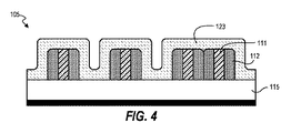
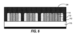
ここで図7を参照すると、充填構造114が次いで基板105上に形成される。充填構造114は、(充填構造114を形成する前に)互いに向き合った第2の側壁スペーサ113の露出した側壁間に規定された開スペースを充填する。充填構造114は、第4の材料で構成される。充填構造114は、マンドレル111の上面、第1の側壁スペーサ112の上面、第2の側壁スペーサ113の上面、及び充填構造114の上面がすべて覆われないように形成される。形成中の材料選択は、第1の材料、第2の材料、第3の材料、及び第4の材料がすべて互いに化学的に異なるようにする。充填構造114を形成することは、第4の材料の過剰材料124を基板上に付着させることを含むことができる。図6は、基板105上に付着した過剰材料124を示し、それは既存の構造を完全に覆うことができる。過剰材料124を付着させるために、スピンオン付着を含め、様々な付着技術が使用され得る。付着後、第4の材料が第2の側壁スペーサ113の上面よりも下に窪むまで、過剰材料124がエッチバックされ得る。第4の材料は、また、第1の側壁スペーサ112の上面及びマンドレル111の上面よりも下に窪む。
Referring now to FIG. 7, filling
図8は、マンドレル111、第1の側壁スペーサ112、第2の側壁スペーサ113、及び充填構造114による4つの異なるラインアレイを有する基板セグメントの斜視図を示す。この結果において、マンドレル111、第1の材料、第2の材料、第3の材料、及び第4の材料は、すべて互いに化学的に異なり、第1のエッチング化学は、残りの材料に対して第1の材料を選択的にエッチングし、第2のエッチング化学は、残りの材料に対して第2の材料を選択的にエッチングし、第3のエッチング化学は、残りの材料に対して第3の材料を選択的にエッチングし、第4のエッチング化学は、残りの材料に関して第4の材料を選択的にエッチングする。言い換えると、4つの異なる材料のいずれも、残りの材料に対して選択的にエッチングされ得る。他の実施形態では、第1の材料、第2の材料、第3の材料、及び第4の材料は、すべて互いに化学的に異なり、所定のエッチング化学を使用してエッチングするときに、所与の2つの材料が残りの材料に対して選択的にエッチングされる。別の実施形態では、第1の材料、第2の材料、第3の材料、及び第4の材料は、すべて互いに化学的に異なり、所定のエッチング化学を使用して基板をエッチングすることは、残りの材料に対して所与の3つの材料を選択的にエッチングすることである。別の実施形態では、第1の材料、第2の材料、第3の材料、及び第4の材料のうちの少なくとも2つの材料が残りの材料とは化学的に異なる。従って、残りの材料に対して1つ以上の選択材料をエッチングする所定のエッチング化学を使用して、エッチングプロセスが実行され得る。
FIG. 8 shows a perspective view of a substrate segment having four different line arrays with a
他の実施形態では、第1の材料、第2の材料、第3の材料、及び第4の材料のうちの2つは同じ材料であり、第1のエッチング化学は、残りの材料に対して第1の材料、第2の材料、第3の材料、及び第4の材料のうちの2つを同時選択的にエッチングする。したがって、すべての異なる材料を有する代わりに、2つ以上の材料は同じ材料であり、それゆえ一致するエッチング特性を本質的に有する。特定の異なる材料が、両方のエッチングに適合する特定の化学で同様にエッチングすることができ、それゆえ、同時にエッチングされ得るフィーチャを作成するための異なる方法が存在する。同じ材料の材料は、例えば、所与の基板上の隣接するライン又は交互にあるラインとすることができる。 In other embodiments, two of the first material, the second material, the third material, and the fourth material are the same material, and the first etch chemistry is relative to the remaining material. Two of the first material, the second material, the third material, and the fourth material are simultaneously and selectively etched. Thus, instead of having all the different materials, the two or more materials are the same material and therefore have essentially matching etching properties. Certain different materials can be similarly etched with specific chemistries that are compatible with both etches, and therefore there are different ways to create features that can be etched simultaneously. Materials of the same material can be, for example, adjacent lines or alternating lines on a given substrate.
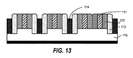
ここで、図9〜図13を参照すると、過剰材料124を窪ませる際に有益となり得る代替的な方法が開示されている。この方法は、第1の側壁スペーサ112を形成するときに、下地層115内にまで部分的にエッチングすることを伴う。図9は、スペーサ・オープン・エッチングが下地層115内にまで部分的にエッチングすることを含むことを除いて、図3と同様である。指向性エッチャントに暴露される下地層115の上面は、今やマンドレル111の底面よりも下にあることに留意されたい。この窪みの利点は、コンフォーマル膜123が比較的高い側壁を有する構造に付着されるため、図10においてより明らかになる。図11は、第1の側壁スペーサ112よりも長い第2の側壁スペーサ113を示す。こうして、過剰材料124が付着されるときには(図12)、第2の側壁スペーサ113間に付着した過剰材料124の量が長くなり、図13に示すように、エッチバックを実行して充填構造114を形成するときにより長くなり、耐性を持たせることを意味する。
Referring now to FIGS. 9-13, an alternative method that may be beneficial in recessing
様々なエッチング化学が4つの材料のうちの1つ以上を選択的にエッチングするために使用され得る。様々な選択比で他のタイプの材料に対して特定のタイプの材料を選択的にエッチングすることができるエッチング化学(プロセスガス及びガスの組み合わせ)が知られている。 Various etching chemistries can be used to selectively etch one or more of the four materials. Etching chemistries (process gases and gas combinations) are known that are capable of selectively etching certain types of materials with respect to other types of materials at various selectivity ratios.
下地層115は、第1の材料、第2の材料、第3の材料及び第4の材料とは化学的に異なる第5の材料で構成され得る。第5の材料が他の4つの材料とは異なることによって、下地層は、他の層に転写するための複合パターンを作成するための記憶層又は転写層として使用され得る。
The
マスキング層を使用すると、パターン転写をさらに助けることができる。図14は、図8の例示的な基板セグメントの上面図である。さらなるパターニング動作のために4つの異なる材料のラインが形成されていることに留意されたい。概して、基板の少なくとも一部分は、セグメント130に示すように、材料タイプパターンがA−B−C−D−C−B−Aであるラインの繰り返しパターンを含むことができる。したがって、材料のタイプに応じて、様々な間隔距離が利用可能である。例えば、材料A又は材料Dの繰り返しインスタンス間には、異なる材料の5つのラインが存在する。これらの材料は、マンドレル材料及び充填構造材料に対応することができる。材料B又は材料Cの繰り返しインスタンス間には、代表的には、異なる材料タイプの1つ又は3つのラインが存在する。
A masking layer can be used to further aid pattern transfer. 14 is a top view of the exemplary substrate segment of FIG. Note that four different lines of material have been formed for further patterning operations. In general, at least a portion of the substrate can include a repeating pattern of lines with a material type pattern of A-B-C-D-C-B-A, as shown in
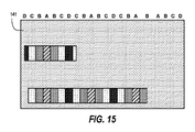
図15に示すように、第1の材料、第2の材料、第3の材料及び第4の材料を覆わない開口を規定する第1のエッチングマスク141が基板上に設けられ得る。そのようなエッチングマスクは、一方向においてより小さい寸法で直線的とすることができる開口を規定することができることに留意されたい。第1のエッチングマスク141及び対応する開口は、従来のフォトリソグラフィシステムによって規定され得る。
As shown in FIG. 15, a
第1の選択材料は、第1のエッチングマスク141及び第1のエッチング化学を使用して選択的にエッチングされる。図16は、この選択的なエッチングの結果の例示的な結果を示す。材料Aのマスクされていない部分が除去され、それらの位置で今や下地層115が見えていることに留意されたい。このエッチングステップ中、残りの材料は除去されなかったことにも留意されたい。図17は、第1のエッチングマスク141が除去された、これらの結果を示す。他の実施形態では、第2の選択材料が、第1のエッチングマスクと第2のエッチング化学を使用して選択的にエッチングされ得る。代替的には、1つ以上の材料が、残りの1つ以上の材料に対して選択的にエッチングされ得る。
The first selective material is selectively etched using the
ここで、図18を参照すると、第1の材料、第2の材料、第3の材料及び第4の材料を覆わない開口を規定する第2のエッチングマスク142が基板上に作成され得る。1つ以上のマスクされていない材料が、次いで、第2のエッチングマスク及び第2のエッチング化学を使用して、残りの材料に対して選択的にエッチングされ得る。図18は、エッチングされた材料Cのマスクされていない部分を示す。図19は、第2のエッチングマスク142が除去された基板セグメントを示す。図20は、下地層を介して複合パターンを転写した結果を示す。図21に示す非限定的な例では、材料B及びDは、保持されているか、又は反転されて、転送されたセグメント又はカットと組み合わされて、図21に示す構造を提供する。マンドレルのピッチは、所与のフォトリソグラフィシステムの光学解像度よりも小さいことに留意されたい。例えば、マンドレルのハーフピッチ間隔は、40ナノメートル未満、12ナノメートル未満、又はそれよりも小さくすることができ、本明細書における技術は、従来のフォトリソグラフィシステムを使用してそのような狭ピッチライン間にカットを生成することができる。
Referring now to FIG. 18, a
4つの材料の同一平面上の表面が望ましい用途には、他の方法が使用され得る。そのような実施形態では、下地層上に位置するマンドレル111を有する基板105を提供することは、2つの材料で構成されるマンドレルを含む。マンドレルの下側部分151は第1の材料で構成され、マンドレルの上側部分152は第6の材料で構成される。この例を図22に示す。第1の材料は、窒化物のような、化学機械研磨に耐性のあるストップ材料層として選択される。図1〜図6において前述したように、プロセスの流れは、次いで、図23に示すように過剰材料124が基板105上に付着する時点まで継続する。この時点でエッチバックを省略してもよいし、部分的に実行してもよい。この実施形態は、マンドレル、第1の側壁スペーサ、第2の側壁スペーサ、及び充填構造を、下方のマンドレルの下側部分151の上面に向けて平坦化する化学機械研磨プロセスを実行することによって基板を平坦化する平坦化ステップを含み、図24に示すように、マンドレルの上面、第1の側壁スペーサの上面、第2の側壁スペーサの上面、及び充填構造の上面がすべて同一平面上にあるようにする。そのような技術の1つの利点は、側壁スペーサの湾曲した、尖った、又は傾斜した表面を除去することである。
Other methods can be used for applications where coplanar surfaces of the four materials are desired. In such an embodiment, providing the
別の実施形態は、半導体基板上のパターン形成された構造を含む。このパターン形成された構造は、4つの異なる材料のラインを有する、基板上のナノ加工構造を含む。4つの異なる材料のラインは、基板の少なくとも一部においてA−B−C−D−C−B−Aの繰り返し配列を規定する。各ラインの上面は覆われておらず、それゆえ指向的にエッチングされ得る。ラインのうちの少なくとも2つは、コンフォーマル付着とそれに続く指向性エッチングを使用した側壁スペーサとして作成されている。それぞれの材料のラインは、16ナノメートル未満のハーフピッチ間隔を有する。4つの異なる材料は、互いに化学的に異なり、1つ以上の材料が残りの材料に対して選択的にエッチングされ得る。図8は、このパターン形成された構造の例示的な実施形態の図示である。このパターン形成された構造は、代表的には最終構造ではなく、その後に続くパターン形成、ピッチ上でのカッティング等のための有効化構造である。 Another embodiment includes a patterned structure on a semiconductor substrate. This patterned structure comprises a nanofabricated structure on a substrate with four different material lines. The four different material lines define a repeating sequence of A-B-C-D-C-B-A on at least a portion of the substrate. The top surface of each line is uncovered and therefore can be directionally etched. At least two of the lines are made as sidewall spacers using conformal deposition followed by directional etching. Each line of material has a half pitch spacing of less than 16 nanometers. The four different materials are chemically different from each other and one or more materials can be selectively etched with respect to the rest of the materials. FIG. 8 is a diagram of an exemplary embodiment of this patterned structure. This patterned structure is typically not the final structure, but an enabling structure for subsequent patterning, pitch-cutting, etc.
理解され得るように、選択可能な材料及び材料の組み合わせのマトリクスが作成されて、従来のフォトリソグラフィシステムの解像度能力よりも小さい所望の位置及び長さでフィーチャを作成することができる。エッチングされたフィーチャそのものは、記憶層及び/又はターゲット層に転写されることができ、パターンを反転するためにも使用され得ることに留意されたい。したがって、選択エッチングのために5つの異なる材料にアクセスすることができる。自己整合がエッチングマスク及び異なる材料の異なるエッチング選択性を使用して、基板上の様々な場所で選択され得る。言い換えると、既知の寸法の4つの異なる材料により、設計者はエッチングを実行する場所を選択し、そのエッチングがサブ解像度の寸法で自己整合するようにすることができる。例えば、フォトレジスト材料による所与のコンタクトパターンが比較的大きく、複数の材料にまたがる場合、コンタクトは、そのコンタクトパターン開口内の材料のうちの1つでのみエッチングされる。 As can be appreciated, a matrix of selectable materials and material combinations can be created to create features at desired locations and lengths that are less than the resolution capabilities of conventional photolithography systems. Note that the etched features themselves can be transferred to the storage layer and/or the target layer and can also be used to invert the pattern. Therefore, five different materials can be accessed for selective etching. Self-alignment can be selected at various locations on the substrate using etch masks and different etch selectivity of different materials. In other words, four different materials of known dimensions allow the designer to choose where to perform the etch and allow the etch to be self-aligned at sub-resolution dimensions. For example, if a given contact pattern of photoresist material is relatively large and spans multiple materials, the contact will only be etched with one of the materials in the contact pattern opening.
本明細書における技術は、ペデスタル化された(pedestalized)カラースキーム、すなわち、異なるエッチング選択性を有する材料を提供するために使用され得る。それ自体がサブ解像度の複数のパターニングの製品であり得るマンドレルから出発して、スペーサ(コンフォーマルな材料)でダブルラップ(double wrapped)され、残りのスペースは第4の材料で充填される。カットの長さは、SADP/SAQP及びALD技術によって制御され、フォトリソグラフィ解像度に対してかなり小さい寸法に制御することができる。例えば、SADP/SAQP技術は、光学的に設定された解像度パターンを開始サイズの8分の1又は16分の1に縮小することができ、スペーサ付着技術はナノメートル以下で制御することができる。従来は、ピッチ上でのカットをすることは非常に難しかった。従来のフォトリソグラフィシステムは、約42ナノメートルのカットを行うことができる。しかし、本明細書における技術により、コンタクトは思いのままに任意の場所に配置又はカットすることができる。このパターニング技法は、色をまたいだピッチ分割も可能にする。いくつかの領域では、マンドレル間のように、材料間に完全なハーフピッチが存在し、他の領域には比較的大きな量の自己整合がある。さらに、2つの材料が互いに隣接している5つの色の材料のうちの2つ以上を選択することによって、図21に示すことができるように、オフピッチ又は混合サイズのエッチングが実行され得る。したがって、本明細書の技術により、様々なピッチ倍数をカット又はブロックとして作成することができる。 The techniques herein may be used to provide pedestalized color schemes, i.e. materials with different etch selectivity. Starting from a mandrel, which itself may be a sub-resolution multiple patterning product, it is double wrapped with spacers (conformal material) and the remaining space is filled with a fourth material. The length of the cut is controlled by SADP/SAQP and ALD techniques and can be controlled to a much smaller dimension for photolithographic resolution. For example, the SADP/SAQP technology can reduce the optically set resolution pattern to one eighth or one sixteenth of the starting size, and the spacer deposition technology can be controlled to sub-nanometers. In the past, it was very difficult to cut on the pitch. Conventional photolithography systems can make cuts of about 42 nanometers. However, the techniques herein allow the contacts to be placed or cut at any location at will. This patterning technique also allows pitch division across colors. In some areas there is a full half pitch between materials, such as between mandrels, and in other areas there is a relatively large amount of self-alignment. Further, by selecting more than one of the five colored materials in which the two materials are adjacent to each other, an off-pitch or mixed size etch can be performed, as can be seen in FIG. Thus, the techniques herein can create various pitch multiples as cuts or blocks.
前述の説明では、処理システムの特定のジオメトリ、及びそこで使用される様々な構成要素及びプロセスの説明等、特定の詳細が明示されている。しかし、本明細書における技術は、これらの特定の詳細から逸脱する他の実施形態において実施されることができ、そのような詳細は、説明を目的とし、限定ではないと理解されるべきである。本明細書において開示された実施形態は、添付の図面を参照して説明されている。同様に、説明を目的として、徹底的な理解を提供するために、特定の数、材料、及び構成が明示されている。それでも、そのような具体的な詳細なしに実施形態を実施することができる。実質的に同一の機能構成を有する構成要素については、類似の符号により示され、任意の冗長説明は省略され得る。 The foregoing description sets forth specific details, such as a description of the particular geometry of the processing system and the various components and processes used therein. It should be understood, however, that the techniques herein may be practiced in other embodiments that depart from these specific details, and that such details are for the purpose of illustration and not limitation. .. The embodiments disclosed herein are described with reference to the accompanying drawings. Similarly, for purposes of explanation, specific numbers, materials, and configurations are set forth to provide a thorough understanding. Nevertheless, embodiments may be practiced without such specific details. Components having substantially the same functional configuration are designated by similar reference numerals, and any redundant description may be omitted.
様々な技術を、様々な実施形態の理解を助けるために複数の離散的な動作として説明した。説明の順序は、これらの操作が必然的に順序に依存することを意味するものとして解釈されるべきではない。実際に、これらの操作は、提示順に実行される必要がない。説明された動作が、説明された実施形態と異なる順序で実行され得る。様々な追加の動作が実行されてもよく、及び/又は説明された動作が追加の実施形態において省略されてもよい。 Various techniques have been described as multiple discrete operations to aid in the understanding of various embodiments. The order of the description should not be construed as implying that these operations are necessarily order-dependent. In fact, these operations do not have to be performed in the order presented. The described acts may be performed in a different order than the described embodiments. Various additional acts may be performed and/or the described acts may be omitted in additional embodiments.
本明細書で使用される「基板」又は「ターゲット基板」は、一般に、本発明に従って処理される物体を指す。基板は、デバイス、特に半導体又は他の電子工学デバイスの任意の材料部分又は構造を含むことができ、例えば、半導体ウェハ、レチクル、又はベース基板構造の上又は上に横たわる薄膜のような層とすることができる。したがって、基板は、いかなる特定のベース構造であること、下地層又は上層であること、及びパターン形成されていること又はパターン形成されていないことには限定されず、むしろそのような層又はベース構造、及び層及び/又はベース構造の任意の組み合わせを含むと考えられる。この説明は、特定のタイプの基板を参照することができるが、これは例示的な目的のみのためである。 "Substrate" or "target substrate" as used herein generally refers to an object that is processed according to the present invention. The substrate can include any material portion or structure of a device, particularly a semiconductor or other electronics device, such as a semiconductor wafer, reticle, or layer such as a thin film overlying or overlying a base substrate structure. be able to. Thus, the substrate is not limited to being any particular base structure, underlayer or overlayer, and patterned or unpatterned, rather such layer or base structure. , And any combination of layers and/or base structures. This description may refer to a particular type of substrate, but this is for illustrative purposes only.
当業者であれば、本発明の同じ目的を依然として達成しつつ、上述した技術の動作に対してなされる多くのバリエーションが存在し得るとも理解するだろう。そのようなバリエーションが本開示の範囲によって網羅されることを意図している。このように、本発明の実施形態の前述の説明が限定することを意図していない。むしろ、本発明の実施形態に対する任意の制限は、以下の特許請求の範囲において提示される。
Those skilled in the art will also understand that there may be many variations to the operation of the above described technique while still accomplishing the same purpose of the invention. Such variations are intended to be covered by the scope of this disclosure. Thus, the above description of embodiments of the present invention is not intended to be limiting. Rather, any limitations to the embodiments of the invention are set out in the following claims.
Claims (19)
下地層上に位置したマンドレルを有する基板を提供するステップであって、該マンドレルは第1の材料で構成される、提供するステップと、
前記マンドレルの露出した側壁に第1の側壁スペーサを形成するステップであって、該第1の側壁スペーサは第2の材料で構成される、形成するステップと、
前記第1の側壁スペーサの露出した側壁に第2の側壁スペーサを形成するステップであって、該第2の側壁スペーサは第3の材料で構成される、形成するステップと、
互いに向き合う前記第2の側壁スペーサの露出した側壁の間に規定された開スペースを充填する充填構造を形成するステップであって、該充填構造は第4の材料で構成され、前記マンドレルの上面、前記第1の側壁スペーサの上面、前記第2の側壁スペーサの上面、及び該充填構造の上面はすべて覆われず、前記第1の材料、前記第2の材料、前記第3の材料及び該第4の材料は、すべて互いに化学的に異なる、形成するステップと、
前記第1の材料、前記第2の材料、前記第3の材料、及び前記第4の材料を覆わない開口を規定する第1のエッチングマスクを前記基板上に設けるステップと、
前記第1のエッチングマスク及び第1のエッチング化学を使用して、第1の選択材料を選択的にエッチングするステップと、を含む方法。 A method of patterning a substrate, the method comprising:
Providing a substrate having a mandrel located on an underlayer, the mandrel comprising a first material; providing;
Forming a first sidewall spacer on the exposed sidewall of the mandrel, the first sidewall spacer being comprised of a second material; forming.
Forming a second sidewall spacer on the exposed sidewall of the first sidewall spacer, the second sidewall spacer being comprised of a third material; and forming.
And forming a filling structure for filling a defined open space between the exposed sidewall of said second sidewall spacers facing each other, said filling structure consists of a fourth material, the top surface of said mandrel, upper surface of said first sidewall spacers, the upper surface of the second sidewall spacers, and the upper surface of the filling structure is not entirely covered, the first material, the second material, the third material and the second 4 materials are all chemically different from each other, forming steps,
Providing a first etching mask on the substrate that defines an opening that does not cover the first material, the second material, the third material, and the fourth material;
Selectively etching a first select material using the first etch mask and a first etch chemistry .
前記第3の材料を前記基板上にコンフォーマルに付着させるステップと、
前記第3の材料を前記マンドレルの上面から、及び前記第1の側壁スペーサの側壁に付着した前記第3の材料の間における前記下地層から除去するスペーサ・オープン・エッチングを実行するステップと、を含む、請求項1に記載の方法。 The step of forming the second sidewall spacer comprises:
Conformally depositing the third material on the substrate;
Performing spacer open etching to remove the third material from the top surface of the mandrel and from the underlying layer between the third materials deposited on the sidewalls of the first sidewall spacers. The method of claim 1, comprising.
過剰な前記第4の材料を前記基板上に付着させるステップと、
前記第4の材料が前記第2の側壁スペーサの上面より下に窪むまで、前記第4の材料をエッチバックするステップと、を含む、請求項1に記載の方法。 Forming the filling structure filling an open space defined between exposed sidewalls of the second sidewall spacers;
Depositing an excess of the fourth material on the substrate;
Etching back the fourth material until the fourth material is recessed below the top surface of the second sidewall spacer.
下地層上に位置したマンドレルを有する基板を提供するステップであって、該マンドレルは2つの材料で構成され、該マンドレルの下側部分は第1の材料で構成され、該マンドレルの上側部分は第6の材料で構成され、前記第1の材料は、化学機械研磨に耐性のあるストップ材料層として選択されている、提供するステップと、
前記マンドレルの露出した側壁に第1の側壁スペーサを形成するステップであって、該第1の側壁スペーサは第2の材料で構成される、形成するステップと、
前記第1の側壁スペーサの露出した側壁に第2の側壁スペーサを形成するステップであって、該第2の側壁スペーサは第3の材料で構成される、形成するステップと
互いに向き合う前記第2の側壁スペーサの露出した側壁の間に規定された開スペースを充填する充填構造を形成するステップであって、該充填構造は第4の材料で構成され、前記マンドレルの上面、前記第1の側壁スペーサの上面、前記第2の側壁スペーサの上面、及び前記充填構造の上面はすべて覆われず、前記第1の材料、前記第2の材料、前記第3の材料及び前記第4の材料のうちの少なくとも2つの材料は、残りの材料に対して化学的に異なる、形成するステップと、を含む方法。 A method of patterning a substrate, the method comprising:
Comprising: providing a substrate having a mandrel positioned on the base layer, the mandrel is composed of two materials, the lower portion of the mandrel is constituted by a first material, the upper portion of the mandrel first 6 materials, said first material being selected as a stop material layer resistant to chemical mechanical polishing , providing.
Forming a first sidewall spacer on the exposed sidewall of the mandrel, the first sidewall spacer being comprised of a second material; forming.
Forming a second sidewall spacer on the exposed sidewall of the first sidewall spacer, the second sidewall spacer being comprised of a third material; and forming.
Forming a filling structure filling an open space defined between exposed sidewalls of said second sidewall spacers facing each other, said filling structure being comprised of a fourth material, the upper surface of said mandrel, The upper surface of the first sidewall spacer, the upper surface of the second sidewall spacer, and the upper surface of the filling structure are not covered, and the first material, the second material, the third material, and the third material are not covered. Forming at least two of the four materials are chemically different from the rest of the materials .
下地層上に位置したマンドレルを有する基板を提供するステップであって、該マンドレルは第1の材料で構成される、提供するステップと、
前記マンドレルの露出した側壁に第1の側壁スペーサを形成するステップであって、該第1の側壁スペーサは第2の材料で構成され、該第1の側壁スペーサを形成するステップは、前記第2の材料を前記基板上にコンフォーマルに付着させるステップと、前記第2の材料を前記マンドレルの上面から、及び前記マンドレルの側壁に付着した前記第2の材料の間における前記下地層から除去するスペーサ・オープン・エッチングを実行するステップと、を含み、該スペーサ・オープン・エッチングを実行するステップは、前記下地層内にまで部分的にエッチングするステップを含む、形成するステップと、
前記第1の側壁スペーサの露出した側壁に第2の側壁スペーサを形成するステップであって、該第2の側壁スペーサは第3の材料で構成される、形成するステップと、
互いに向き合う前記第2の側壁スペーサの露出した側壁の間に規定された開スペースを充填する充填構造を形成するステップであって、該充填構造は第4の材料で構成され、前記マンドレルの上面、前記第1の側壁スペーサの上面、前記第2の側壁スペーサの上面、及び前記充填構造の上面はすべて覆われず、前記第1の材料、前記第2の材料、前記第3の材料及び前記第4の材料のうちの少なくとも2つの材料は、残りの材料に対して化学的に異なる、形成するステップと、を含む方法。 A method of patterning a substrate, the method comprising:
Providing a substrate having a mandrel located on an underlayer, the mandrel comprising a first material; providing;
And forming a first sidewall spacer on the exposed sidewall of said mandrel, said first sidewall spacer is composed of a second material, the step of forming said first sidewall spacers, said second Conformally depositing the material on the substrate, and removing the second material from the top surface of the mandrel and from the underlying layer between the second materials deposited on the sidewalls of the mandrel. - performing a open etch, only including the step of executing the spacer open etching comprises the steps of said containing partially step of etching until the underlying layer is formed,
Forming a second sidewall spacer on the exposed sidewall of the first sidewall spacer, the second sidewall spacer being comprised of a third material; and forming.
Forming a filling structure filling an open space defined between exposed sidewalls of said second sidewall spacers facing each other, said filling structure being comprised of a fourth material, the upper surface of said mandrel, The upper surface of the first sidewall spacer, the upper surface of the second sidewall spacer, and the upper surface of the filling structure are not covered, and the first material, the second material, the third material, and the third material are not covered. Forming at least two of the four materials are chemically different from the rest of the materials .
下地層上に位置したマンドレルを有する基板を提供するステップであって、該マンドレルは第1の材料で構成される、提供するステップと、
前記マンドレルの露出した側壁に第1の側壁スペーサを形成するステップであって、前記第1の側壁スペーサは第2の材料で構成される、形成するステップと、
前記第1の側壁スペーサの露出した側壁に第2の側壁スペーサを形成するステップであって、前記第2の側壁スペーサは第3の材料で構成される、形成するステップと、
互いに向き合う前記第2の側壁スペーサの露出した側壁の間に規定された開スペースを充填する充填構造を形成するステップであって、該充填構造は第4の材料で構成され、前記マンドレルの上面、前記第1の側壁スペーサの上面、前記第2の側壁スペーサの上面、及び該充填構造の上面はすべて覆われず、前記第1の材料、前記第2の材料、前記第3の材料及び該第4の材料のうちの少なくとも2つの材料は、残りの材料に対して化学的に異なる、形成するステップと、
前記第1の材料、前記第2の材料、前記第3の材料、及び前記第4の材料を覆わない開口を規定する第1のエッチングマスクを前記基板上に設けるステップと、
前記第1のエッチングマスク及び第1のエッチング化学を使用して、残りの材料に対して1つ以上の材料を選択的にエッチングするステップと、を含む方法。 A method of patterning a substrate, the method comprising:
Providing a substrate having a mandrel located on an underlayer, the mandrel comprising a first material; providing;
Forming a first side wall spacer on the exposed side wall of the mandrel, the first side wall spacer comprising a second material; forming.
Forming a second sidewall spacer on the exposed sidewall of the first sidewall spacer, the second sidewall spacer being comprised of a third material; forming;
And forming a filling structure for filling a defined open space between the exposed sidewall of said second sidewall spacers facing each other, said filling structure consists of a fourth material, the top surface of said mandrel, upper surface of said first sidewall spacers, the upper surface of the second sidewall spacers, and the upper surface of the filling structure is not entirely covered, the first material, the second material, the third material and the second Forming at least two of the four materials are chemically different from the rest of the materials .
Providing a first etching mask on the substrate that defines an opening that does not cover the first material, the second material, the third material, and the fourth material;
Selectively etching one or more materials with respect to the remaining material using the first etching mask and the first etching chemistry .
前記第1の材料、前記第2の材料、前記第3の材料、及び前記第4の材料を覆わない開口を規定する第2のエッチングマスクを前記基板上に設けるステップと、
前記第2のエッチングマスク及び第2のエッチング化学を使用して、残りの材料に対して1つ以上の材料を選択的にエッチングするステップと、さらに含む、請求項17に記載の方法。 And removing the pre-Symbol first etching mask,
Providing a second etching mask on the substrate that defines an opening that does not cover the first material, the second material, the third material, and the fourth material;
18. The method of claim 17 , further comprising selectively etching one or more materials with respect to the remaining material using the second etching mask and a second etching chemistry.
4つの異なる材料のラインを有する、基板上のナノ加工構造であって、4つ異なる材料の該ラインは、該基板の少なくとも一部においてA−B−C−D−C−B−Aの繰り返し配列を規定し、各ラインの上面が覆われておらず、4つの異なる材料の該ラインのうち少なくとも2つは、マンドレル上のコンフォーマル付着とそれに続く指向性エッチングとを使用した側壁スペーサとして作成されており、少なくとも1つのラインは充填構造として形成されている、ナノ加工構造を含み、
前記マンドレルは、16ナノメートル未満のハーフピッチ間隔を有し、
4つの異なる材料の前記ラインは互いに化学的に異なり、1つ以上の材料が残りの材料に対して選択的にエッチングされ得る、構造。
A structure formed on a semiconductor substrate by patterning,
A nanofabricated structure on a substrate having four different material lines, wherein the four different material lines are repeated A-B-C-D-C-B-A in at least a portion of the substrate. An array is defined, where the top of each line is uncovered and at least two of the four different materials are made as sidewall spacers using conformal deposition on the mandrel followed by directional etching. A nanofabricated structure, wherein at least one line is formed as a filling structure ,
The mandrel has a half pitch spacing of less than 16 nanometers,
A structure in which the lines of four different materials are chemically different from each other and one or more materials may be selectively etched with respect to the rest of the materials.
Applications Claiming Priority (5)
| Application Number | Priority Date | Filing Date | Title |
|---|---|---|---|
| US201562232005P | 2015-09-24 | 2015-09-24 | |
| US62/232,005 | 2015-09-24 | ||
| US201562258119P | 2015-11-20 | 2015-11-20 | |
| US62/258,119 | 2015-11-20 | ||
| PCT/US2016/052668 WO2017053296A1 (en) | 2015-09-24 | 2016-09-20 | Methods of forming etch masks for sub-resolution substrate patterning |
Publications (3)
| Publication Number | Publication Date |
|---|---|
| JP2018530156A JP2018530156A (en) | 2018-10-11 |
| JP2018530156A5 JP2018530156A5 (en) | 2019-08-15 |
| JP6726834B2 true JP6726834B2 (en) | 2020-07-22 |
Family
ID=58386992
Family Applications (2)
| Application Number | Title | Priority Date | Filing Date |
|---|---|---|---|
| JP2018515551A Active JP6726834B2 (en) | 2015-09-24 | 2016-09-20 | Method for forming an etching mask for sub-resolution substrate patterning |
| JP2018515554A Pending JP2018531506A (en) | 2015-09-24 | 2016-09-20 | Method of forming an etching mask for sub-resolution substrate patterning |
Family Applications After (1)
| Application Number | Title | Priority Date | Filing Date |
|---|---|---|---|
| JP2018515554A Pending JP2018531506A (en) | 2015-09-24 | 2016-09-20 | Method of forming an etching mask for sub-resolution substrate patterning |
Country Status (6)
| Country | Link |
|---|---|
| US (2) | US9818611B2 (en) |
| JP (2) | JP6726834B2 (en) |
| KR (1) | KR102436100B1 (en) |
| CN (2) | CN108352304B (en) |
| TW (2) | TWI620995B (en) |
| WO (2) | WO2017053296A1 (en) |
Families Citing this family (39)
| Publication number | Priority date | Publication date | Assignee | Title |
|---|---|---|---|---|
| US9564312B2 (en) | 2014-11-24 | 2017-02-07 | Lam Research Corporation | Selective inhibition in atomic layer deposition of silicon-containing films |
| KR102207120B1 (en) * | 2016-01-29 | 2021-01-22 | 도쿄엘렉트론가부시키가이샤 | Method and system for forming a memory pin pattern |
| US9991156B2 (en) * | 2016-06-03 | 2018-06-05 | International Business Machines Corporation | Self-aligned quadruple patterning (SAQP) for routing layouts including multi-track jogs |
| US10629435B2 (en) | 2016-07-29 | 2020-04-21 | Lam Research Corporation | Doped ALD films for semiconductor patterning applications |
| US10002762B2 (en) * | 2016-09-09 | 2018-06-19 | International Business Machines Corporation | Multi-angled deposition and masking for custom spacer trim and selected spacer removal |
| US9911619B1 (en) * | 2016-10-12 | 2018-03-06 | Globalfoundries Inc. | Fin cut with alternating two color fin hardmask |
| US10832908B2 (en) * | 2016-11-11 | 2020-11-10 | Lam Research Corporation | Self-aligned multi-patterning process flow with ALD gapfill spacer mask |
| US10454029B2 (en) | 2016-11-11 | 2019-10-22 | Lam Research Corporation | Method for reducing the wet etch rate of a sin film without damaging the underlying substrate |
| US9881794B1 (en) | 2016-11-29 | 2018-01-30 | Taiwan Semiconductor Manufacturing Company, Ltd. | Semiconductor methods and devices |
| US10388644B2 (en) | 2016-11-29 | 2019-08-20 | Taiwan Semiconductor Manufacturing Company, Ltd. | Method of manufacturing conductors and semiconductor device which includes conductors |
| BR112019010217A2 (en) * | 2016-12-23 | 2019-08-27 | Intel Corp | advanced lithography and self-assembled devices |
| US9934970B1 (en) * | 2017-01-11 | 2018-04-03 | International Business Machines Corporation | Self aligned pattern formation post spacer etchback in tight pitch configurations |
| US10217633B2 (en) * | 2017-03-13 | 2019-02-26 | Globalfoundries Inc. | Substantially defect-free polysilicon gate arrays |
| CN108735585B (en) * | 2017-04-17 | 2019-06-28 | 联华电子股份有限公司 | The production method of mask pattern |
| US10304728B2 (en) * | 2017-05-01 | 2019-05-28 | Advanced Micro Devices, Inc. | Double spacer immersion lithography triple patterning flow and method |
| US20180323061A1 (en) * | 2017-05-03 | 2018-11-08 | Tokyo Electron Limited | Self-Aligned Triple Patterning Process Utilizing Organic Spacers |
| CN109216163A (en) * | 2017-06-29 | 2019-01-15 | 中芯国际集成电路制造(上海)有限公司 | The manufacturing method of semiconductor devices |
| US10147611B1 (en) * | 2017-08-28 | 2018-12-04 | Nanya Technology Corporation | Method for preparing semiconductor structures |
| US10269559B2 (en) | 2017-09-13 | 2019-04-23 | Lam Research Corporation | Dielectric gapfill of high aspect ratio features utilizing a sacrificial etch cap layer |
| CN109545684B (en) * | 2017-09-22 | 2020-11-27 | 中芯国际集成电路制造(上海)有限公司 | Semiconductor structure and forming method thereof |
| US10340364B2 (en) | 2017-11-14 | 2019-07-02 | International Business Machines Corporation | H-shaped VFET with increased current drivability |
| US10566207B2 (en) * | 2017-12-27 | 2020-02-18 | Samsung Electronics Co., Ltd. | Semiconductor manufacturing methods for patterning line patterns to have reduced length variation |
| US11404275B2 (en) | 2018-03-02 | 2022-08-02 | Lam Research Corporation | Selective deposition using hydrolysis |
| US10395926B1 (en) * | 2018-04-17 | 2019-08-27 | Globalfoundries Inc. | Multiple patterning with mandrel cuts formed using a block mask |
| JP2019204815A (en) * | 2018-05-21 | 2019-11-28 | 東京エレクトロン株式会社 | Substrate processing method and substrate processing apparatus |
| US10643846B2 (en) | 2018-06-28 | 2020-05-05 | Lam Research Corporation | Selective growth of metal-containing hardmask thin films |
| US10763118B2 (en) * | 2018-07-11 | 2020-09-01 | International Business Machines Corporation | Cyclic selective deposition for tight pitch patterning |
| US10910381B2 (en) * | 2018-08-01 | 2021-02-02 | Applied Materials, Inc. | Multicolor approach to DRAM STI active cut patterning |
| CN110911272B (en) * | 2018-09-17 | 2024-05-03 | 长鑫存储技术有限公司 | Method for forming micro pattern in semiconductor device |
| US11164772B2 (en) * | 2018-10-30 | 2021-11-02 | International Business Machines Corporation | Spacer-defined process for lithography-etch double patterning for interconnects |
| EP3660890B1 (en) | 2018-11-27 | 2021-08-11 | IMEC vzw | A method for forming an interconnection structure |
| CN111370309B (en) * | 2018-12-26 | 2023-12-12 | 中芯国际集成电路制造(上海)有限公司 | Semiconductor structure and forming method thereof |
| CN111640655B (en) * | 2019-03-01 | 2023-04-25 | 中芯国际集成电路制造(上海)有限公司 | Semiconductor device and method of forming the same |
| US10943816B2 (en) | 2019-04-03 | 2021-03-09 | International Business Machines Corporation | Mask removal for tight-pitched nanostructures |
| US11315787B2 (en) * | 2019-04-17 | 2022-04-26 | Applied Materials, Inc. | Multiple spacer patterning schemes |
| CN111952165A (en) * | 2019-05-17 | 2020-11-17 | 中芯国际集成电路制造(上海)有限公司 | Semiconductor structure and forming method thereof |
| CN112017970B (en) * | 2020-07-24 | 2022-09-20 | 中国科学院微电子研究所 | Method for manufacturing self-aligned metal layer, semiconductor device and electronic equipment |
| US11990409B2 (en) | 2021-04-19 | 2024-05-21 | Samsung Electronics Co., Ltd. | Semiconductor device with fine metal lines for BEOL structure and method of manufacturing the same |
| CN118039463A (en) * | 2024-01-19 | 2024-05-14 | 深圳市鹏芯微集成电路制造有限公司 | Mask manufacturing method and semiconductor device manufacturing method |
Family Cites Families (28)
| Publication number | Priority date | Publication date | Assignee | Title |
|---|---|---|---|---|
| US5223083A (en) | 1992-01-23 | 1993-06-29 | Micron Technology, Inc. | Process for etching a semiconductor device using an improved protective etching mask |
| JP2827882B2 (en) * | 1994-02-24 | 1998-11-25 | 日本電気株式会社 | Method for manufacturing semiconductor device |
| US6632741B1 (en) * | 2000-07-19 | 2003-10-14 | International Business Machines Corporation | Self-trimming method on looped patterns |
| US7190007B2 (en) * | 2004-08-05 | 2007-03-13 | International Business Machines Corporation | Isolated fully depleted silicon-on-insulator regions by selective etch |
| US7560390B2 (en) * | 2005-06-02 | 2009-07-14 | Micron Technology, Inc. | Multiple spacer steps for pitch multiplication |
| US7696101B2 (en) * | 2005-11-01 | 2010-04-13 | Micron Technology, Inc. | Process for increasing feature density during the manufacture of a semiconductor device |
| KR101348280B1 (en) * | 2007-07-06 | 2014-01-10 | 삼성전자주식회사 | Method of forming fine pitch hardmask and method of fine patterns of semiconductor device |
| US8852851B2 (en) * | 2006-07-10 | 2014-10-07 | Micron Technology, Inc. | Pitch reduction technology using alternating spacer depositions during the formation of a semiconductor device and systems including same |
| US7611980B2 (en) * | 2006-08-30 | 2009-11-03 | Micron Technology, Inc. | Single spacer process for multiplying pitch by a factor greater than two and related intermediate IC structures |
| US7666578B2 (en) * | 2006-09-14 | 2010-02-23 | Micron Technology, Inc. | Efficient pitch multiplication process |
| KR20080034234A (en) * | 2006-10-16 | 2008-04-21 | 삼성전자주식회사 | Method of forming fine patterns in semiconductor device |
| WO2008115600A1 (en) * | 2007-03-21 | 2008-09-25 | Olambda, Inc. | Multi-material hard mask or prepatterned layer for use with multi-patterning photolithography |
| US7923373B2 (en) * | 2007-06-04 | 2011-04-12 | Micron Technology, Inc. | Pitch multiplication using self-assembling materials |
| US7994495B2 (en) * | 2008-01-16 | 2011-08-09 | Xerox Corporation | Organic thin film transistors |
| JP2010080625A (en) * | 2008-09-25 | 2010-04-08 | Toshiba Corp | Method of forming mask pattern, and method of manufacturing semiconductor device |
| JP4825891B2 (en) * | 2009-03-31 | 2011-11-30 | 株式会社東芝 | Semiconductor device manufacturing method and template |
| KR101732936B1 (en) * | 2011-02-14 | 2017-05-08 | 삼성전자주식회사 | Method for forming fine patterns of a semiconductor device |
| CN102693898B (en) * | 2011-03-21 | 2016-02-24 | 华邦电子股份有限公司 | Contract closely spaced method |
| JP2013161987A (en) * | 2012-02-06 | 2013-08-19 | Toshiba Corp | Pattern formation method |
| US9034197B2 (en) * | 2012-09-13 | 2015-05-19 | HGST Netherlands B.V. | Method for separately processing regions on a patterned medium |
| US9153477B2 (en) * | 2012-09-28 | 2015-10-06 | Intel Corporation | Directed self assembly of block copolymers to form vias aligned with interconnects |
| CN103715068A (en) * | 2012-09-29 | 2014-04-09 | 中芯国际集成电路制造(上海)有限公司 | Forming method of semiconductor fine pattern |
| US8871651B1 (en) * | 2013-07-12 | 2014-10-28 | Globalfoundries Inc. | Mask formation processing |
| US9041217B1 (en) * | 2013-12-18 | 2015-05-26 | Intel Corporation | Self-aligned via patterning with multi-colored photobuckets for back end of line (BEOL) interconnects |
| US9209077B2 (en) * | 2013-12-20 | 2015-12-08 | Intel Corporation | Diagonal hardmasks for improved overlay in fabricating back end of line (BEOL) interconnects |
| KR102176758B1 (en) * | 2014-02-10 | 2020-11-10 | 에스케이하이닉스 주식회사 | Structure and method for forming pattern using block copolymer materials |
| WO2015126812A1 (en) * | 2014-02-23 | 2015-08-27 | Tokyo Electron Limited | Method for multiplying pattern density by crossing multiple patterned layers |
| CN103943468A (en) * | 2014-05-08 | 2014-07-23 | 上海华力微电子有限公司 | Self-aligning forming method for figure |
-
2016
- 2016-09-20 WO PCT/US2016/052668 patent/WO2017053296A1/en active Application Filing
- 2016-09-20 CN CN201680067753.1A patent/CN108352304B/en active Active
- 2016-09-20 US US15/270,717 patent/US9818611B2/en active Active
- 2016-09-20 CN CN201680067813.XA patent/CN108292591A/en active Pending
- 2016-09-20 KR KR1020187010710A patent/KR102436100B1/en active IP Right Grant
- 2016-09-20 JP JP2018515551A patent/JP6726834B2/en active Active
- 2016-09-20 JP JP2018515554A patent/JP2018531506A/en active Pending
- 2016-09-20 WO PCT/US2016/052694 patent/WO2017053316A1/en active Application Filing
- 2016-09-20 US US15/270,841 patent/US10020196B2/en active Active
- 2016-09-22 TW TW105130524A patent/TWI620995B/en active
- 2016-09-22 TW TW105130522A patent/TWI622861B/en active
Also Published As
| Publication number | Publication date |
|---|---|
| CN108292591A (en) | 2018-07-17 |
| US20170092506A1 (en) | 2017-03-30 |
| JP2018530156A (en) | 2018-10-11 |
| TW201721292A (en) | 2017-06-16 |
| TWI620995B (en) | 2018-04-11 |
| CN108352304B (en) | 2022-03-08 |
| KR102436100B1 (en) | 2022-08-24 |
| WO2017053316A1 (en) | 2017-03-30 |
| TW201721293A (en) | 2017-06-16 |
| US20170092496A1 (en) | 2017-03-30 |
| KR20180049101A (en) | 2018-05-10 |
| US9818611B2 (en) | 2017-11-14 |
| CN108352304A (en) | 2018-07-31 |
| KR20180045892A (en) | 2018-05-04 |
| JP2018531506A (en) | 2018-10-25 |
| TWI622861B (en) | 2018-05-01 |
| US10020196B2 (en) | 2018-07-10 |
| WO2017053296A1 (en) | 2017-03-30 |
Similar Documents
| Publication | Publication Date | Title |
|---|---|---|
| JP6726834B2 (en) | Method for forming an etching mask for sub-resolution substrate patterning | |
| US11107682B2 (en) | Method for patterning a substrate using a layer with multiple materials | |
| KR102603019B1 (en) | Method for forming an etch mask for sub-resolution substrate patterning | |
| JP2018531506A6 (en) | Method of forming an etching mask for sub-resolution substrate patterning | |
| KR102296805B1 (en) | How to pattern a substrate using layers with multiple materials | |
| TWI633583B (en) | Method and system for forming memory fin patterns | |
| CN109075124B (en) | Method for patterning a substrate using a layer having multiple materials | |
| JP2019537266A (en) | Sub-resolution substrate patterning method | |
| KR102705674B1 (en) | Method for forming an etching mask for sub-resolution substrate patterning |
Legal Events
| Date | Code | Title | Description |
|---|---|---|---|
| A521 | Request for written amendment filed |
Free format text: JAPANESE INTERMEDIATE CODE: A523 Effective date: 20190708 |
|
| A621 | Written request for application examination |
Free format text: JAPANESE INTERMEDIATE CODE: A621 Effective date: 20190708 |
|
| TRDD | Decision of grant or rejection written | ||
| A01 | Written decision to grant a patent or to grant a registration (utility model) |
Free format text: JAPANESE INTERMEDIATE CODE: A01 Effective date: 20200414 |
|
| A711 | Notification of change in applicant |
Free format text: JAPANESE INTERMEDIATE CODE: A711 Effective date: 20200511 |
|
| A61 | First payment of annual fees (during grant procedure) |
Free format text: JAPANESE INTERMEDIATE CODE: A61 Effective date: 20200511 |
|
| R150 | Certificate of patent or registration of utility model |
Ref document number: 6726834 Country of ref document: JP Free format text: JAPANESE INTERMEDIATE CODE: R150 |
|
| R250 | Receipt of annual fees |
Free format text: JAPANESE INTERMEDIATE CODE: R250 |
|
| R250 | Receipt of annual fees |
Free format text: JAPANESE INTERMEDIATE CODE: R250 |